WO2011122494A1 - 液晶表示装置、画素回路、および駆動方法 - Google Patents
液晶表示装置、画素回路、および駆動方法 Download PDFInfo
- Publication number
- WO2011122494A1 WO2011122494A1 PCT/JP2011/057454 JP2011057454W WO2011122494A1 WO 2011122494 A1 WO2011122494 A1 WO 2011122494A1 JP 2011057454 W JP2011057454 W JP 2011057454W WO 2011122494 A1 WO2011122494 A1 WO 2011122494A1
- Authority
- WO
- WIPO (PCT)
- Prior art keywords
- sub
- liquid crystal
- trunk line
- potential
- reference potential
- Prior art date
- Legal status (The legal status is an assumption and is not a legal conclusion. Google has not performed a legal analysis and makes no representation as to the accuracy of the status listed.)
- Ceased
Links
Images

















Classifications
-
- G—PHYSICS
- G09—EDUCATION; CRYPTOGRAPHY; DISPLAY; ADVERTISING; SEALS
- G09G—ARRANGEMENTS OR CIRCUITS FOR CONTROL OF INDICATING DEVICES USING STATIC MEANS TO PRESENT VARIABLE INFORMATION
- G09G3/00—Control arrangements or circuits, of interest only in connection with visual indicators other than cathode-ray tubes
- G09G3/20—Control arrangements or circuits, of interest only in connection with visual indicators other than cathode-ray tubes for presentation of an assembly of a number of characters, e.g. a page, by composing the assembly by combination of individual elements arranged in a matrix no fixed position being assigned to or needed to be assigned to the individual characters or partial characters
- G09G3/34—Control arrangements or circuits, of interest only in connection with visual indicators other than cathode-ray tubes for presentation of an assembly of a number of characters, e.g. a page, by composing the assembly by combination of individual elements arranged in a matrix no fixed position being assigned to or needed to be assigned to the individual characters or partial characters by control of light from an independent source
- G09G3/36—Control arrangements or circuits, of interest only in connection with visual indicators other than cathode-ray tubes for presentation of an assembly of a number of characters, e.g. a page, by composing the assembly by combination of individual elements arranged in a matrix no fixed position being assigned to or needed to be assigned to the individual characters or partial characters by control of light from an independent source using liquid crystals
- G09G3/3611—Control of matrices with row and column drivers
- G09G3/3648—Control of matrices with row and column drivers using an active matrix
- G09G3/3655—Details of drivers for counter electrodes, e.g. common electrodes for pixel capacitors or supplementary storage capacitors
-
- G—PHYSICS
- G02—OPTICS
- G02F—OPTICAL DEVICES OR ARRANGEMENTS FOR THE CONTROL OF LIGHT BY MODIFICATION OF THE OPTICAL PROPERTIES OF THE MEDIA OF THE ELEMENTS INVOLVED THEREIN; NON-LINEAR OPTICS; FREQUENCY-CHANGING OF LIGHT; OPTICAL LOGIC ELEMENTS; OPTICAL ANALOGUE/DIGITAL CONVERTERS
- G02F1/00—Devices or arrangements for the control of the intensity, colour, phase, polarisation or direction of light arriving from an independent light source, e.g. switching, gating or modulating; Non-linear optics
- G02F1/01—Devices or arrangements for the control of the intensity, colour, phase, polarisation or direction of light arriving from an independent light source, e.g. switching, gating or modulating; Non-linear optics for the control of the intensity, phase, polarisation or colour
- G02F1/13—Devices or arrangements for the control of the intensity, colour, phase, polarisation or direction of light arriving from an independent light source, e.g. switching, gating or modulating; Non-linear optics for the control of the intensity, phase, polarisation or colour based on liquid crystals, e.g. single liquid crystal display cells
- G02F1/133—Constructional arrangements; Operation of liquid crystal cells; Circuit arrangements
- G02F1/1333—Constructional arrangements; Manufacturing methods
- G02F1/1343—Electrodes
- G02F1/134309—Electrodes characterised by their geometrical arrangement
-
- G—PHYSICS
- G09—EDUCATION; CRYPTOGRAPHY; DISPLAY; ADVERTISING; SEALS
- G09G—ARRANGEMENTS OR CIRCUITS FOR CONTROL OF INDICATING DEVICES USING STATIC MEANS TO PRESENT VARIABLE INFORMATION
- G09G3/00—Control arrangements or circuits, of interest only in connection with visual indicators other than cathode-ray tubes
- G09G3/20—Control arrangements or circuits, of interest only in connection with visual indicators other than cathode-ray tubes for presentation of an assembly of a number of characters, e.g. a page, by composing the assembly by combination of individual elements arranged in a matrix no fixed position being assigned to or needed to be assigned to the individual characters or partial characters
- G09G3/34—Control arrangements or circuits, of interest only in connection with visual indicators other than cathode-ray tubes for presentation of an assembly of a number of characters, e.g. a page, by composing the assembly by combination of individual elements arranged in a matrix no fixed position being assigned to or needed to be assigned to the individual characters or partial characters by control of light from an independent source
- G09G3/36—Control arrangements or circuits, of interest only in connection with visual indicators other than cathode-ray tubes for presentation of an assembly of a number of characters, e.g. a page, by composing the assembly by combination of individual elements arranged in a matrix no fixed position being assigned to or needed to be assigned to the individual characters or partial characters by control of light from an independent source using liquid crystals
- G09G3/3607—Control arrangements or circuits, of interest only in connection with visual indicators other than cathode-ray tubes for presentation of an assembly of a number of characters, e.g. a page, by composing the assembly by combination of individual elements arranged in a matrix no fixed position being assigned to or needed to be assigned to the individual characters or partial characters by control of light from an independent source using liquid crystals for displaying colours or for displaying grey scales with a specific pixel layout, e.g. using sub-pixels
-
- G—PHYSICS
- G02—OPTICS
- G02F—OPTICAL DEVICES OR ARRANGEMENTS FOR THE CONTROL OF LIGHT BY MODIFICATION OF THE OPTICAL PROPERTIES OF THE MEDIA OF THE ELEMENTS INVOLVED THEREIN; NON-LINEAR OPTICS; FREQUENCY-CHANGING OF LIGHT; OPTICAL LOGIC ELEMENTS; OPTICAL ANALOGUE/DIGITAL CONVERTERS
- G02F1/00—Devices or arrangements for the control of the intensity, colour, phase, polarisation or direction of light arriving from an independent light source, e.g. switching, gating or modulating; Non-linear optics
- G02F1/01—Devices or arrangements for the control of the intensity, colour, phase, polarisation or direction of light arriving from an independent light source, e.g. switching, gating or modulating; Non-linear optics for the control of the intensity, phase, polarisation or colour
- G02F1/13—Devices or arrangements for the control of the intensity, colour, phase, polarisation or direction of light arriving from an independent light source, e.g. switching, gating or modulating; Non-linear optics for the control of the intensity, phase, polarisation or colour based on liquid crystals, e.g. single liquid crystal display cells
- G02F1/133—Constructional arrangements; Operation of liquid crystal cells; Circuit arrangements
- G02F1/1333—Constructional arrangements; Manufacturing methods
- G02F1/1343—Electrodes
- G02F1/134309—Electrodes characterised by their geometrical arrangement
- G02F1/134345—Subdivided pixels, e.g. for grey scale or redundancy
-
- G—PHYSICS
- G09—EDUCATION; CRYPTOGRAPHY; DISPLAY; ADVERTISING; SEALS
- G09G—ARRANGEMENTS OR CIRCUITS FOR CONTROL OF INDICATING DEVICES USING STATIC MEANS TO PRESENT VARIABLE INFORMATION
- G09G3/00—Control arrangements or circuits, of interest only in connection with visual indicators other than cathode-ray tubes
- G09G3/20—Control arrangements or circuits, of interest only in connection with visual indicators other than cathode-ray tubes for presentation of an assembly of a number of characters, e.g. a page, by composing the assembly by combination of individual elements arranged in a matrix no fixed position being assigned to or needed to be assigned to the individual characters or partial characters
- G09G3/2007—Display of intermediate tones
- G09G3/2074—Display of intermediate tones using sub-pixels
Definitions
- the present invention relates to a liquid crystal display device, a pixel circuit, and a driving method.
- This application claims priority based on Japanese Patent Application No. 2010-075784 filed in Japan on March 29, 2010, the contents of which are incorporated herein by reference.
- liquid crystal display devices are required to have high image quality, and a multi-pixel method is used in which one pixel is divided into two sub-pixels and gradation is controlled in units of sub-pixels (see, for example, Patent Document 1). .
- one pixel is composed of two electrically equivalent sub-pixels.
- the gradation expression is controlled by changing the potential of each auxiliary capacitor Cs connected to the two sub-pixels and causing a potential difference in each sub-pixel.
- a counter matrix configuration has been proposed as a configuration method of the liquid crystal display device (see, for example, Patent Document 2).
- a scan bus line, an installation bus line, a switching element, and a display electrode are provided on a first glass substrate.
- a transparent electrode that is also used as a data bus line is provided on the second glass substrate.
- data bus lines and scan bus lines are not stacked. Therefore, the frequency of occurrence of short-circuit defects between layers is greatly reduced and the yield is good as compared with the configuration other than the facing matrix configuration.
- the counter matrix configuration can perform inspection and repair (repair) only on each glass substrate, the yield is good.
- Patent Document 2 does not describe multi-pixel formation. Further, the multi-pixel method according to the prior art of Patent Document 1 does not describe the counter matrix configuration.
- the present invention has been made in view of the above-described problems, and an object of the present invention is to provide a liquid crystal display device, a pixel circuit, and a driving method in which a multi-pixel is configured with a counter matrix.
- the liquid crystal element is formed between the first substrate and the second substrate, and each of the n sub-pixels One pole of the liquid crystal element of the first display And the other pole of the liquid crystal element of each of the n sub-pixels is connected to the nth reference potential trunk line from the first reference potential trunk line via each of the switching elements, and the control The unit supplies an on-state signal from the scanning line to the switching elements of the n sub-pixels at the same timing.
- control unit may switch the polarity of the potential of the first display signal line for each frame.
- control unit sets the potential magnitude in order from the first reference potential trunk to the nth reference potential trunk and from the nth reference potential trunk to the first reference. You may make it switch alternately for every flame
- the control unit switches the potential of the first display signal line for each frame around a predetermined reference potential, and sets the magnitude of the potential to a predetermined level. Centering on the reference potential, a predetermined voltage amplitude is added, and alternately in order from the first reference potential trunk line to the nth reference potential trunk line and from the nth reference potential trunk line to the first reference potential trunk line. You may make it switch.
- the liquid crystal display device further includes a second display signal line that supplies a display signal, and the n sub-pixels are arranged adjacent to each other in the row direction.
- One of the liquid crystal elements of each of the sub-pixels is connected to the second display signal line, and the other is connected to the nth reference potential trunk line from the first reference potential trunk line via each of the switching elements.
- the control unit may alternately switch the polarities of the potentials of the first display signal line and the second display signal line for each frame.
- pixels including n subpixels and n subpixels arranged adjacent to each other in the row direction are arranged in a matrix.
- One of the liquid crystal elements of the sub-pixel of the pixel adjacent to the sub-pixel of the liquid crystal element in the row direction is connected to the second display signal line, and the other is connected to the first ′ reference potential main line via the switching element.
- One of the liquid crystal elements of the sub-pixel of the pixel adjacent to the sub-pixel of the liquid crystal element connected in the row direction to the sub-pixel of the liquid crystal element connected to the second reference trunk line via the switching element is the second display signal line In
- the other is connected to the second reference potential trunk line via the switching element, and the control unit relates the relationship between the magnitude of the potential of the first reference potential trunk line and the magnitude of the potential of the first 'reference trunk line. May be switched alternately for each frame.
- the control unit is configured so that the potential of the first reference potential trunk line is larger than the potential of the first 'reference trunk line.
- the potential of the reference trunk line is alternately switched for each frame so that the potential of the reference trunk line is greater than the potential of the first reference potential trunk line, or the polarity of the potential of the first 'reference trunk line and the polarity of the potential of the first reference potential trunk line May be alternately replaced for each frame.
- pixels each including the n sub-pixels and n sub-pixels arranged adjacent to each other in the row direction are arranged in a matrix.
- the liquid crystal element of the sub-pixel of the pixel adjacent to the sub-pixel of the liquid crystal element connected to the first reference trunk line via the switching element in the row direction is one of the second display signals.
- One of the liquid crystal elements of the sub-pixel of the pixel to be connected is connected to the second display signal line, the other is connected to the second reference potential trunk line through the switching element, and the third element is connected to the third reference potential trunk line through the switching element.
- One of the liquid crystal elements of the sub-pixel of the pixel adjacent to the sub-pixel of the liquid crystal element connected to the reference trunk line in the row direction is connected to the second display signal line, and the other is connected to the second display signal line via the switching element.
- control unit determines the relationship between the magnitude of the potential of the first reference potential trunk line and the magnitude of the potential of the first ′ reference trunk line, and the potential of the third reference potential trunk line. You may make it switch a magnitude
- control unit may be configured such that the potential of the first reference potential trunk line is greater than the potential of the first 'reference trunk line and the third reference potential. Since the potential of the trunk line is greater than the potential of the third 'reference trunk line, the potential of the first' reference trunk line is greater than the potential of the first reference potential trunk line and the potential of the third 'reference trunk line. Are alternately switched every frame so that the potential of the first reference potential trunk line is greater than the potential of the third reference potential trunk line, or the potential of the first 'reference trunk line is greater than the potential of the first reference potential trunk line and the third potential.
- the potential of the reference potential trunk line is greater than the potential of the third 'reference trunk line
- the potential of the first reference potential trunk line is greater than the potential of the first' reference trunk line and the third 'reference trunk line.
- the potential of the third group is It may be switched alternately every frame a larger relationship potential of trunk.
- each of the sub-pixels of the pixel in the s (s is a positive integer) row has s ⁇ 1 rows with respect to the nth reference potential trunk line. You may make it arrange
- N reference potential trunk lines having different potential magnitudes, a first display signal line for supplying a display signal, a scanning line, and a control unit, and each of the liquid crystal elements of each of the n sub-pixels.
- One pole is the first display signal
- the other pole of the liquid crystal element of each of the n sub-pixels is connected from the first reference potential trunk line to the nth reference potential trunk line via the switching element, and the control unit Supplies an on-state signal from the scanning line to the switching elements of each of the n sub-pixels at the same timing.
- a driving method includes a first substrate on which a first reference potential trunk line to an nth reference potential trunk line and a switching element are arranged, and a first display signal.
- n sub-pixels n ⁇ 2, n is a positive integer
- each of the sub-pixels has a switching element
- each of the sub-pixels has a liquid crystal element
- the first reference potential trunk line to the n-th reference potential trunk line have a potential of N reference potential trunk lines having different sizes
- a first display signal line for supplying a display signal, a scanning line, and a control unit, and one of the liquid crystal elements of each of the n sub-pixels.
- the pole is connected to the first display signal line
- the other pole of the liquid crystal element of each of the n sub-pixels is connected to the nth reference potential trunk line from the first reference potential trunk line via the switching element
- the control unit includes: An on-state signal is supplied from the scanning line to the switching element of each of the n sub-pixels at the same timing.
- the first reference potential trunk line to the nth reference potential trunk line and the switching element are disposed on the first reference potential trunk line and the second substrate on which the first display signal line is disposed.
- the driving method of the liquid crystal display device in which the liquid crystal element is formed between the pixels is composed of n pixels (n ⁇ 2, n is a positive integer) corresponding to a plurality of luminance regions in a matrix.
- pixels composed of n (n ⁇ 2, n is a positive integer) subpixels corresponding to a plurality of luminance regions are arranged in a matrix.
- a liquid crystal element is formed between the first substrate and the second substrate.
- each liquid crystal element of the n sub-pixels is connected to the first display signal line, and the other pole of each liquid crystal element of the n sub-pixels is connected to the first display signal line via each switching element.
- the first reference potential trunk line is connected to the nth reference potential trunk line.
- a control part supplies the signal of an ON state from a scanning line to each switching element of n sub pixel at the same timing. Therefore, it is possible to perform a liquid crystal display device, a pixel circuit, and a driving method that form a multi-pixel with a counter matrix.
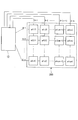
- FIG. 6 It is a perspective view of an example of a liquid crystal display device to which an embodiment of the present invention is applied. It is a block diagram of an example of the liquid crystal display device to which embodiment of this invention is applied.
- 6 is an equivalent circuit for explaining an operation in an L frame of a liquid crystal display device including two sub-pixels according to the first embodiment.
- 4 is an equivalent circuit for explaining an operation in an L + 1 frame of a liquid crystal display device including two subpixels according to the embodiment.
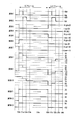
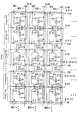
- 6 is a timing chart of the liquid crystal display device at the L frame and the L + 1 frame according to the embodiment. It is a figure explaining an example of the layout on the 1st board
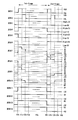
- 6 is a timing chart of the liquid crystal display device at the L frame and the L + 1 frame according to the embodiment. It is an equivalent circuit explaining the operation
- 4 is an equivalent circuit for explaining an operation in an L + 1 frame of a liquid crystal display device including three sub-pixels according to the embodiment.
- 6 is a timing chart of the liquid crystal display device at the L frame and the L + 1 frame according to the embodiment. It is an equivalent circuit explaining the operation
- 4 is an equivalent circuit for explaining an operation in an L + 1 frame of a liquid crystal display device including n (even) sub-pixels according to the embodiment.
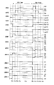
- 6 is a timing chart of the liquid crystal display device at the L frame and the L + 1 frame according to the embodiment.
- FIG. 1 is a perspective view of an example of a liquid crystal display device to which an embodiment of the present invention is applied.
- the liquid crystal display device according to the embodiment of the present invention includes a first substrate 10, a second substrate 20 disposed to face the first substrate 10, and a control unit 12.
- a liquid crystal material is sealed between the first substrate 10 and the second substrate 20.
- the first substrate 10 includes a switching element 2 made up of a plurality of thin film transistors (TFTs), a plurality of reference potential trunk lines 4, a plurality of scanning lines (gate bus lines) 5, and a display electrode 11.
- TFTs thin film transistors
- gate bus lines gate bus lines
- the second substrate 20 includes a striped transparent electrode 13.
- the transparent electrodes 13 are connected to display signal lines (data bus lines) 3, respectively.
- the switching element 2, the reference potential trunk line 4, the scanning line 5, and the display electrode 11 are formed on the first substrate 10.
- Striped transparent electrodes 13 connected to the display signal lines 3 are formed on the opposing second substrate 20. Thereby, an opposing matrix is configured. Further, a non-illustrated backlight is disposed under the first substrate 10.
- FIG. 2 is a configuration diagram of an example of a liquid crystal display device to which the embodiment of the present invention is applied.
- m display signal lines data bus lines
- n scanning lines gate bus lines
- n ⁇ m pixels p (1 , 1) to p (1, m), p (2,1) to p (2, m)... P (n, 1) to p (n, m)).
- the pixel unit 200 is configured by n ⁇ m pixels.
- control unit 12 controls the display signal supplied to the display signal line 3 to have a reverse polarity between the adjacent display signal lines 3. That is, the polarities of the display signal on the display signal line 3-1 and the display signal on the display signal line 3-2 are opposite. Further, the polarities of the display signal of the display signal line 3-2 and the display signal of the display signal line 3-3 are opposite. Further, the polarities of the display signal of the display signal line 3-3 and the display signal of the display signal line 3-4 are opposite.
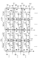
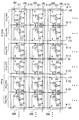
- FIG. 3 shows the operation of the liquid crystal display device having the pixels (Pix (n ⁇ 1), Pix (n)) having two sub-pixels (Sub-Pix1, Sub-Pix2) in the first embodiment at the L frame. It is an equivalent circuit to explain.
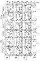
- FIG. 4 shows the operation of the liquid crystal display device having the pixels (Pix (n ⁇ 1), Pix (n)) including two sub-pixels (Sub-Pix1, Sub-Pix2) in the first embodiment at the L + 1 frame. It is an equivalent circuit to explain. Note that one frame is 1/60 second in a liquid crystal display device driven at 60 Hz, for example. As shown in FIG. 3, the liquid crystal display device according to the first embodiment includes pixels 101 to 106.
- Each of the pixels 101 to 106 includes two subpixels.
- the pixel 101 and the pixel 102 are arranged adjacent to each other in the row direction.
- the pixel 101 is arranged in the order of the sub pixel 111 and the sub pixel 112 in the column direction from the reference potential trunk line 4-1.
- the pixel 102 is arranged in the order of the sub-pixel 121 and the sub-pixel 122 in the column direction from the reference potential trunk line 4-1.
- the pixel 104 and the pixel 105 arranged adjacent to each other in the row direction are arranged symmetrically with the pixel 101 and the pixel 102 with respect to the reference potential trunk line 4-2.
- the pixel 104 is arranged in the order of the sub-pixel 142 and the sub-pixel 141 in the column direction from the reference potential trunk line 4-1.
- the pixel 105 is arranged in the order of the sub-pixel 152 and the sub-pixel 151 in the column direction from the reference potential trunk line 4-1.
- the sub-pixel is each pixel obtained by dividing one pixel into a plurality of pixels.
- the pixel 101 corresponds to R
- the pixel 102 corresponds to G
- the pixel 103 corresponds to B.
- each sub-pixel is composed of a liquid crystal element 1, a switching element 2, and a stripe-shaped transparent electrode 13 facing the liquid crystal element 1.
- the liquid crystal element is composed of a liquid crystal material sandwiched between one display electrode and the striped transparent electrode 13, and is expressed as an electric capacity as an electrical equivalent circuit.
- the sub-pixel 111 includes a liquid crystal element 1-11 and a switching element 2-11.
- the sub-pixel 112 includes a liquid crystal element 1-12 and a switching element 2-12. Note that the display electrode 11 and the stripe-shaped transparent electrode 13 opposed to the display electrode 11 are equivalently expressed as electrical connection portions to the liquid crystal elements 1-11 and 1-12 in FIG.
- the gate terminals of the switching element 2-11 and the switching element 2-12 are connected to a common scanning line 5-1.
- the source terminal of the switching element 2-11 is connected to the reference potential trunk line 4-1.
- the drain terminal of the switching element 2-11 is connected to one of the liquid crystal elements 1-11 having a capacitive component via the display electrode 11.
- the other side of the liquid crystal element 1-11 is connected to a display signal line (first display signal line) 3-1 through the transparent electrode 13. That is, the liquid crystal element 1-11 is sandwiched between the transparent electrode 13 and the electrode 11.
- the source terminal of the switching element 2-12 is connected to the reference potential trunk line 4-2.
- the drain terminal of the switching element 2-12 is connected to one of the liquid crystal elements 1-12 through the display electrode 11.
- the other side of the liquid crystal element 1-12 is connected to the display signal line 3-1 through the transparent electrode 13.
- configurations of the sub-pixel 121 and the sub-pixel 122 of the pixel 102 will be described.
- the gate terminals of the switching element 2-21 and the switching element 2-22 are connected to a common scanning line 5-1.
- the source terminal of the switching element 2-21 is connected to the reference potential trunk line 4-1.
- the drain terminal of the switching element 2-21 is connected to one of the liquid crystal elements 1-21 through the display electrode 11.
- the other side of the liquid crystal element 1-21 is connected to a display signal line (second display signal line) 3-2 through the transparent electrode 13.
- the gate terminals of the switching elements 2-41 and 2-42 are connected to a common scanning line 5-2.
- the source terminal of the switching element 2-42 is connected to the reference potential trunk line 4-1.
- the drain terminal of the switching element 2-42 is connected to one of the liquid crystal elements 1-42 through the display electrode 11.
- the other side of the liquid crystal element 1-42 is connected to the display signal line 3-1 through the transparent electrode 13.
- the source terminal of the switching element 2-41 is connected to the reference potential trunk line 4-2.
- the drain terminal of the switching element 2-41 is connected to one of the liquid crystal elements 1-41 through the display electrode 11.
- the other side of the liquid crystal element 1-41 is connected to the display signal line 3-1 through the transparent electrode 13.
- the gate terminals of the switching element 2-51 and the switching element 2-52 are connected to a common scanning line 5-2.
- the source terminal of the switching element 2-52 is connected to the reference potential trunk line 4-1.
- the drain terminal of the switching element 2-52 is connected to one of the liquid crystal elements 1-52 through the display electrode 11.
- the other side of the liquid crystal element 1-52 is connected to the display signal line 3-2 through the transparent electrode 13.
- the source terminal of the switching element 2-51 is connected to the reference potential trunk line 4-2.
- the drain terminal of the switching element 2-51 is connected to one of the liquid crystal elements 1-51 through the display electrode 11.
- the other side of the liquid crystal element 1-51 is connected to the display signal line 3-2 through the transparent electrode 13.
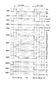
- FIG. 5 is a timing chart of the liquid crystal display device in the L frame and the L + 1 frame in the first embodiment.
- the operation of each subpixel of the pixels 101 to 106 in the L frame (L is a natural number of 1 or more) will be described.
- the horizontal axis indicates time, and the vertical axis indicates potential.
- a waveform 1 in FIG. 5 shows a temporal change in the potential of the scanning line 5-1.
- a waveform 2 in FIG. 5 shows a time change of the potential of the scanning line 5-2.
- a waveform 3 in FIG. 5 shows a time change of the potential of the reference potential trunk line 4-1.
- a waveform 5 in FIG. 5 shows a temporal change in the potential of the reference potential trunk line 4-2.
- a waveform 5 in FIG. 5 shows a time change of the potential of the display signal line 3-1.
- a waveform 6 in FIG. 5 shows a time change of the potential of the display signal line 3-2.
- a waveform 7 in FIG. 5 shows a time change of the potential of the node X (node X).
- a waveform 8 in FIG. 5 shows a temporal change in the potential of the node Y (node Y).
- a waveform 9 in FIG. 5 shows a change with time of the potential of the node X-node Y (node-pix1 applied voltage).
- the control unit 12 controls the potential of the reference potential trunk line 4-1 to +1 V and controls the potential of the reference potential trunk line 4-2 to 0 V (waveform 3 and waveform 4 in FIG. 5, time t0a). That is, the control unit 12 controls the magnitude of the potential so that the potential of the reference potential trunk line 4-1 is larger than the potential of the reference potential trunk line 4-2.
- the control unit 12 controls the scanning line 5-1 to H level during the period from time t0a to t1a (rewriting period for one pixel), and switching elements 2-11 to 2-12 and 2-21 to 2 ⁇ 22 and 2-31 to 2-32 are turned on. Note that the period during which the output of the scanning line 5-1 is H is set according to the total number of reference potential trunk lines 3 used in the liquid crystal display device.
- the control unit 12 supplies + 5V to the pixel 101 in the first row from the display signal line 3-1 and + 4V to the pixel 104 in the second row, and the pixel 102 in the first row from the display signal line 3-2.
- -4V is supplied to the pixels 105 in the second row.
- the signal range when the maximum gradation is displayed from the zero gradation is, for example, a positive polarity side potential of +5 V to +1 V and a negative polarity side potential of -5 V to ⁇ 1 V. This signal level may be adjusted to the characteristics of the liquid crystal element used.
- the signal levels of the display signal line 3-1 and the display signal line 3-2 shown in FIG. 5 are signal levels showing an example of operation.
- the control unit 12 controls the scanning line 5-2 to the H level during the period of time t1a to t2a, so that the switching elements 2-41 to 2-42, 2-51 to 2-52, and 2-61 to 2 are controlled. -62 is turned on.
- the control unit 12 controls the light transmittance of each sub-pixel by controlling the light transmittance. Key expression) is controlled.
- the control unit 12 controls luminance (gradation expression) by controlling the light reflectance of each sub-pixel.
- the switching elements 2-41 to 2-42 connected to the pixels 104 in the second row are in the OFF state as shown in FIG. 5 during the period from the time t0a to t1a, the potential difference is maintained.
- the switching element 2-12 is turned on, and the liquid crystal element 1-12 (equivalent electric capacity) has + 5V for the display signal line 3-1 and 0V for the reference potential trunk line 4-2. And a potential difference of +5 V is generated.
- the luminance of the sub-pixels 111 to 112 is displayed higher than that of the sub-pixel 111 in the sub-pixel 112 having a larger potential difference. For this reason, the subpixel 111 is dark and the subpixel 112 is brightly displayed.
- a potential difference + 5 V is generated in the liquid crystal element 1-32 (equivalent electric capacity) of the sub-pixel 132 as in the case of the sub-pixel 112. Therefore, the sub pixel 131 is dark and the sub pixel 132 is brightly displayed.
- the luminance of the sub-pixels 141 to 142 is displayed so that the sub-pixel 142 is dark and the sub-pixel 141 is bright.
- a potential difference + 4 V is generated in the liquid crystal element 1-61 (equivalent electric capacity) of the sub-pixel 161 of the pixel 106.
- a potential difference of +3 V is generated in the liquid crystal element 1-62 (equivalent electric capacity) of the sub-pixel 162. Therefore, the sub pixel 162 is dark and the sub pixel 161 is brightly displayed.
- the time chart after time t0b is an L + 1 frame timing chart.
- the control unit 12 switches the polarity of the potentials of the display signal lines 3-1 to 3-3 to a polarity opposite to that in the L frame during the vertical blanking period. Then, the control unit 12 switches the potential of the reference potential trunk line 4-1 from +1 V to 0 V, and switches the potential of the reference potential trunk line 4-2 from 0 V to +1 V (waveform 3 and waveform 4, time t0b in FIG. 5).
- control unit 12 determines that the potential of the reference potential trunk line 4-2 is higher than the potential of the reference potential trunk line 4-2 because the potential is larger than the potential of the reference potential trunk line 4-2. Switch to a relationship that is greater than 1 potential.
- This control means that the potentials of the reference potential trunk lines 4-1 and 4-2 are switched for each frame, and the potentials of both are exchanged for each frame. Note that switching the potential of the reference potential trunk line 4-2 to a phase opposite to that of the reference potential trunk line 4-1 means that the potential of the reference potential trunk line 4-1 is + 1V and the potential of the reference potential trunk line 4-2 is 0V.
- the control unit 12 controls the scanning line 5-1 to the H level during the period from time t0b to t1b, so that the switching elements 2-11 to 2-12, 2-21 to 2-22, and 2-31 to 2-32 is turned on. Therefore, the control unit 12 supplies a ⁇ 4V signal to the first row of pixels 101 from the display signal line 3-1, and supplies a + 5V signal to the first row of pixels 102 from the display signal line 3-2. .
- control unit 12 controls the scanning line 5-2 to the H level during the period of time t1b to t2b, so that the switching elements 2-41 to 2-42, 2-51 to 2-52, and 2-61 to 2 are controlled. -62 is turned on. Therefore, the control unit 12 supplies a ⁇ 3V signal to the pixels 104 in the second row from the display signal line 3-1, and supplies a + 4V signal to the pixels 105 in the second row from the display signal line 3-2. .
- a potential difference generated in each liquid crystal element when each switching element is turned on will be described.
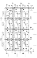
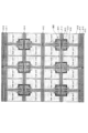
- FIG. 6 is a diagram for explaining an example of the layout on the first substrate 10 to which the first embodiment is applied.
- the hatched area same as the area A11 indicates the first electrode (gate electrode).
- the region hatched in the same manner as the region A12 represents the second electrode (source electrode, drain electrode).
- a region hatched in the same manner as the region A13 indicates a semiconductor layer (silicon layer).
- the hatched area same as the area A14 indicates the third electrode (pixel electrode).
- a portion indicated by a region A15 indicates a contact between the first electrode and the second electrode.
- a portion indicated by a region A16 indicates a contact between the second electrode and the third electrode.
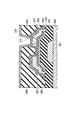
- FIG. 7 shows a cross-sectional view of an amorphous silicon TFT currently used in a general liquid crystal television.
- the TFT includes a glass substrate 500, a gate electrode 501, a gate insulating film 502, an amorphous silicon layer 503 (region A13 in FIGS. 6 and 13), an n + amorphous silicon layer 504, and a source electrode 505 (regions in FIGS. 6 and 13).
- A12) / drain electrode 506 region A13 in FIGS. 6 and 13
- protective film 507, planarizing film 508, and pixel electrode 509 region A14 in FIGS. 6 and 13 are sequentially stacked.
- the pixel electrode 509 and the drain electrode 506 are electrically connected in a contact region 510 (region A16 in FIGS. 6 and 13).
- the glass substrate 500 may be a flexible substrate such as a stainless steel substrate.
- the amorphous silicon layer 503 may be made of a transparent amorphous oxide semiconductor typified by polysilicon, microcrystalline silicon, or IGZO (indium zinc composite oxide). However, in the case where a transparent amorphous oxide semiconductor is used as the amorphous silicon layer 503, the n + amorphous silicon layer may be omitted.
- each pixel includes Sub-pix1 and Sub-pix2.
- the gate terminal of each switching element 2 is connected to the scanning line 5-1 or 5-2.
- the source terminal of the switching element 2 of the sub-pixel Sub-pix1 is connected to the reference potential trunk line 4-1.
- the drain terminal of the switching element 2 of the sub-pixel Sub-pix 1 is connected to one of the liquid crystal elements 1 via the display electrode 11.
- the other side of the liquid crystal element 1 is connected to the display signal line 3 through the transparent electrode 13. Further, the source terminal of the switching element 2 of the sub-pixel Sub-pix2 is connected to the reference potential trunk line 4-2. Further, the drain terminal of the switching element 2 of the sub-pixel Sub-pix 2 is connected to one of the liquid crystal elements 1 via the display electrode 11. The other side of the liquid crystal element 1 is connected to the display signal line 3 through the transparent electrode 13.
- the example in which the magnitudes of the potentials of the reference potential trunk lines 4-1 to 4-3 are switched for each frame has been described. However, it may be for each pixel selection period.
- the pixel selection period is, for example, every 1/60/1080 (seconds) in a display device with 60 Hz drive and resolution Full-HD (having 1080 scanning lines).
- the pixel selection period is defined as 1H, the potential may be switched every 2 kH (k is an integer of 1 or more).
- the second embodiment is another embodiment of a liquid crystal display device in which one pixel is composed of two subpixels.
- FIG. 8 shows the operation of the liquid crystal display device having the pixels (Pix (n ⁇ 1), Pix (n)) having two sub-pixels (Sub-Pix1, Sub-Pix2) in the second embodiment at the time of the L frame. It is an equivalent circuit to explain.
- FIG. 9 shows the operation of the liquid crystal display device having the pixels (Pix (n ⁇ 1), Pix (n)) having two sub-pixels (Sub-Pix1, Sub-Pix2) in the second embodiment at the L + 1 frame. It is an equivalent circuit to explain. As shown in FIG. 8, the circuit configuration is the same as that of the first embodiment.
- the control unit 12 controls the reference potential trunk line 4-1 to + 1V and controls the reference potential trunk line 4-2 to 0V.
- the control unit 12 controls the scanning line 5-1 to the H level and turns on the switching elements 2-11 to 2-12, 2-21 to 2-22, and 2-31 to 2-32. To do.
- the control unit 12 supplies a signal of +5 V (maximum gradation) from the display signal line 3-1 to the pixel 101 in the first row. Further, a + 4V (halftone) signal is supplied from the display signal line 3-2 to the pixels 102 in the first row.
- a signal of +1 V (minimum gradation) is supplied from the display signal line 3-3 to the pixels 103 in the first row. That is, the signal potential for displaying the maximum gradation is centered around + 5V, the positive polarity side is assigned + 1V to + 5V, and the negative polarity side is assigned to + 5V to + 9V. Further, a voltage amplitude of ⁇ 4V is added to the reference potential trunk line 4-1, centered on + 5V, and a voltage amplitude of ⁇ 5V is added to the reference potential trunk line 4-2, centered on + 5V.
- control unit 12 controls the scanning line 5-2 to the H level to turn on the switching elements 2-41 to 2-42, 2-51 to 2-52, and 2-61 to 2-62. . Then, the control unit 12 supplies a signal of + 5V (maximum gradation) from the display signal line 3-1 to the pixel 104 in the second row. Further, a + 4V (halftone) signal is supplied from the display signal line 3-2 to the pixels 105 in the second row. Further, a signal of +1 V (minimum gradation) is supplied from the display signal line 3-3 to the pixels 106 in the second row. Note that the signal levels of the display signal lines 3-1 to 3-3 shown in FIG. 8 are signal levels indicating an example of operation. Hereinafter, a potential difference generated in each liquid crystal element when each switching element is turned on will be described.
- the operation of the sub-pixel 111 and the sub-pixel 112 of the pixel 101 will be described. While the switching element 2-11 is on, a potential difference of + 5V between the display signal line 3-1 and + 1V of the reference potential trunk line 4-1 is generated in the liquid crystal element 1-11. Further, while the switching element 2-12 is on, a potential difference of + 5V between the display signal line 3-1 and + 0V of the reference potential trunk line 4-2 is generated in the liquid crystal element 1-12. As a result, the luminance of the sub-pixels 111 to 112 is displayed so that the sub-pixel 111 is dark and the sub-pixel 112 is bright.
- the control unit 12 switches the reference potential trunk 4-1 from + 1V to + 9V, switches the reference potential trunk 4-2 from 0V to + 10V, and switches the reference potential trunk 4-3 from + 1V to + 9V.
- the control unit 12 controls the scanning line 5-1 to the H level, and turns on the switching elements 2-11 to 2-12, 2-21 to 2-22, and 2-31 to 2-32. To do.
- the control unit 12 supplies a signal of +5 V (maximum gradation) from the display signal line 3-1 to the pixel 101 in the first row. Further, a + 6V (halftone) signal is supplied from the display signal line 3-2 to the pixels 102 in the first row.
- a signal of +9 V is supplied from the display signal line 3-3 to the pixels 103 in the first row.
- the control unit 12 controls the scanning line 5-2 to the H level and turns on the switching elements 2-41 to 2-42, 2-51 to 2-52, and the switching elements 2-61 to 2-62.
- the control unit 12 supplies a signal of +5 V (maximum gradation) from the display signal line 3-1 to the second row 104.
- a + 6V (halftone) signal is supplied from the display signal line 3-2 to the pixels 104 in the second row.
- a signal of +9 V (minimum gradation) is supplied from the display signal line 3-3 to the pixels 106 in the second row.
- the example in which the magnitudes of the potentials of the reference potential trunk lines 4-1 to 4-3 are switched for each frame has been described. However, it may be for each pixel selection period.
- the pixel selection period is, for example, every 1/60/1080 (seconds) in a display device with 60 Hz drive and resolution Full-HD (having 1080 scanning lines).
- the pixel selection period is defined as 1H, the potential may be switched every 2 kH (k is an integer of 1 or more).
- a liquid crystal display device having a multi-pixel facing matrix can be realized.
- a bright pixel one of two sub-pixels having a larger absolute value of the potential difference applied to both ends of the liquid crystal element
- a dark pixel Of the two sub-pixels, the row direction arrangement of the smaller potential value applied to both ends of the liquid crystal element can be arranged in parallel to the scanning line 5-1. Therefore, in addition to the effects of the first embodiment, it is possible to improve display characteristics.
- the third embodiment is another embodiment of a liquid crystal display device in which one pixel is composed of two subpixels.
- FIG. 10 shows the operation of the liquid crystal display device having the pixels (Pix (n ⁇ 1), Pix (n)) having two sub-pixels (Sub-Pix1, Sub-Pix2) in the third embodiment at the time of the L frame. It is an equivalent circuit to explain.
- FIG. 11 shows the operation of the liquid crystal display device having pixels (Pix (n ⁇ 1), Pix (n)) having two sub-pixels (Sub-Pix1, Sub-Pix2) in the third embodiment at the L + 1 frame. It is an equivalent circuit to explain.
- the liquid crystal display device according to the third embodiment includes pixels 101 to 106.
- Each of the pixels 101 to 106 further includes two subpixels.
- the pixel 101 and the pixel 102 are arranged adjacent to each other in the row direction.
- the pixel 101 is arranged in the order of the sub pixel 111 and the sub pixel 112 in the column direction from the reference potential trunk line 4-1.
- the pixel 102 is arranged in the order of the sub-pixel 121 and the sub-pixel 122 in the column direction from the reference potential trunk line (first reference potential trunk line) 4-1.
- the pixels 104 and 105 arranged adjacent to each other in the row direction are arranged symmetrically with the pixel 101 and the pixel 102 with respect to the reference potential trunk line (second reference potential trunk line) 4-2.
- the pixel 104 is arranged in the order of the sub-pixel 142 and the sub-pixel 141 in the column direction from the reference potential trunk line 4-1.
- the pixel 105 is arranged in the order of the sub-pixel 152 and the sub-pixel 151 in the column direction from the reference potential trunk line 4-1. The same applies to the configuration of the pixels 103 and 106.
- the configuration of the sub-pixel 111 and the sub-pixel 112 of the pixel 101 is the same as that in the first embodiment.
- configurations of the sub-pixel 121 and the sub-pixel 122 of the pixel 102 will be described.
- the gate terminals of the switching element 2-21 and the switching element 2-22 are connected to a common scanning line 5-1.
- the source terminal of the switching element 2-21 is connected to a reference potential trunk line (first ′ reference potential trunk line) 4-3.
- the drain terminal of the switching element 2-21 is connected to one of the liquid crystal elements 1-21 through the display electrode 11.
- the other side of the liquid crystal element 1-21 is connected to a display signal line (second display signal line) 3-2 through the transparent electrode 13.
- the source terminal of the switching element 2-22 is connected to the reference potential trunk line 4-2.
- the drain terminal of the switching element 2-22 is connected to one of the liquid crystal elements 1-22 through the display electrode 11.
- the other side of the liquid crystal element 1-22 is connected to the display signal line 3-2 through the transparent electrode 13.
- the configurations of the sub-pixel 141 and the sub-pixel 142 of the pixel 104 are the same as those in the first embodiment.
- configurations of the sub-pixel 151 and the sub-pixel 152 of the pixel 105 are described.
- the gate terminals of the switching elements 2-51 and 2-52 are connected to a common scanning line 5-2.
- the source terminal of the switching element 2-52 is connected to the reference potential trunk line 4-3.
- the drain terminal of the switching element 2-52 is connected to one of the liquid crystal elements 1-52 through the display electrode 11.
- the other side of the liquid crystal element 1-52 is connected to the display signal line 3-2 through the transparent electrode 13.
- the source terminal of the switching element 2-51 is connected to the reference potential trunk line 4-2.
- the drain terminal of the switching element 2-51 is connected to one of the liquid crystal elements 1-51 through the display electrode 11.
- the other side of the liquid crystal element 1-51 is connected to the display signal line 3-2 through the transparent electrode 13.
- FIG. 12 is a timing chart of the liquid crystal display device for the L frame and the L + 1 frame in the third embodiment.
- L is a natural number of 1 or more
- the horizontal axis indicates time
- the vertical axis indicates potential.
- a waveform 1 in FIG. 12 shows a temporal change in the potential of the scanning line 5-1.
- a waveform 2 in FIG. 12 shows a time change of the potential of the scanning line 5-2.
- a waveform 3 in FIG. 12 shows a time change of the potential of the reference potential trunk line 4-1.
- a waveform 12 shows a time change of the potential of the reference potential trunk line 4-2.
- a waveform 5 in FIG. 12 shows a temporal change in the potential of the reference potential trunk line 4-3.
- a waveform 6 in FIG. 12 shows a time change of the potential of the display signal line 3-1.
- a waveform 7 in FIG. 12 shows a time change of the potential of the display signal line 3-2.
- a waveform 8 in FIG. 12 shows a temporal change in the potential of the node X (node X).
- a waveform 9 in FIG. 12 shows a time change of the potential of the node Y (node Y).
- a waveform 10 in FIG. 12 shows a temporal change in the potential of the node X ⁇ node Y (node X-node Y) (applied voltage of Sub-pix1).
- the control unit 12 supplies a + 5V signal to the first row of pixels 101 from the display signal line 3-1, and supplies a -5V signal to the first row of pixels 102 from the display signal line 3-2. .
- the signal ranges of the display signal lines 3-1 to 3-3 are, for example, positive polarity side + 5V to + 1V and negative polarity side -5V to -1V.
- the control unit 12 controls the scanning line 5-2 to the H level during the period of time t1b to t2b, so that the switching elements 2-41 to 2-42, 2-51 to 2-52, and 2-61 to 2 are controlled. -62 is turned on.
- the control unit 12 supplies a + 4V signal from the display signal line 3-1 to the pixels 104 in the second row, and supplies a -4V signal from the display signal line 3-2 to the pixels 105 in the second row.
- the signal levels of the display signal lines 3-1 and 3-2 shown in FIG. 12 are signal levels showing an example of the operation.
- a potential difference generated in each liquid crystal element when each switching element is turned on will be described.
- the control unit 12 supplies the display signal line 3-3 with a display signal having the same polarity as that of the display signal line 3-1.
- the time chart after time t0b is a timing chart of L + 1 frame.
- the control unit 12 switches the polarity of the potentials of the display signal lines 3-1 to 3-3 to a polarity opposite to that in the L frame during the vertical blanking period. Then, the control unit 12 switches the reference potential trunk line 4-1 from + 1V to -1V, and switches the reference potential trunk line 4-3 from -1V to + 1V (FIG. 12, time t0b). That is, the control unit 12 switches the potentials of the reference potential trunk lines 4-1 and 4-2 for each frame and exchanges the potentials of both for each frame.
- the control unit 12 determines the potential magnitude so that the potential of the reference potential trunk line 4-1 is larger than the potential of the reference potential trunk line 4-2, and the potential of the reference potential trunk line 4-2 is equal to the reference potential trunk line 4. Therefore, the potential of the reference potential trunk line 4-3 is greater than the potential of the reference potential trunk line 4-2, and the potential of the reference potential trunk line 4-2 is equal to the reference potential trunk line 4-1. Switch to a relationship that is greater than the potential.
- the control unit 12 controls the scanning line 5-1 to the H level during the period from time t0b to t1b, so that the switching elements 2-11 to 2-12, 2-21 to 2-22, and 2-31 to 2-32 is turned on.
- the control unit 12 supplies a ⁇ 5V signal to the first row of pixels 101 from the display signal line 3-1, and supplies a + 5V signal to the first row of pixels 102 from the display signal line 3-2. . Further, the control unit 12 controls the scanning line 5-2 to the H level during the period of time t1b to t2b, so that the switching elements 2-41 to 2-42, 2-51 to 2-52, and 2-61 to 2 are controlled. -62 is turned on. Therefore, the control unit 12 supplies a ⁇ 4V signal to the second row of pixels 104 from the display signal line 3-1, and supplies a + 4V signal to the second row of pixels 105 from the display signal line 3-2. .
- a potential difference generated in each liquid crystal element when each switching element is turned on will be described.
- the luminance of the sub-pixels 141 to 142 is displayed darker in the sub-pixel 142 and brighter in the sub-pixel 141 according to the potential difference.
- FIG. 13 is a diagram for explaining an example of the layout on the first substrate 10 to which the third embodiment is applied.
- the hatched area same as the area A ⁇ b> 11 represents the first electrode (gate electrode).
- the region hatched in the same manner as the region A12 represents the second electrode (source electrode, drain electrode).
- a region hatched in the same manner as the region A13 indicates a semiconductor layer (silicon layer).
- the hatched area same as the area A14 indicates the third electrode (pixel electrode).
- a portion indicated by a region A15 indicates a contact between the first electrode and the second electrode.
- a portion indicated by a region A16 indicates a contact between the second electrode and the third electrode.
- each pixel includes Sub-pix1 and Sub-pix2.
- the gate terminal of each switching element 2 is connected to the scanning line 5-1 or 5-2.
- the source terminal of the switching element 2 of the sub-pixel Sub-pix1 is connected to the reference potential trunk line 4-1 or the reference potential trunk line 4-3.
- the drain terminal of the switching element 2 of the sub-pixel Sub-pix 1 is connected to one of the liquid crystal elements 1 through the display electrode 11.
- the other side of the liquid crystal element 1 is connected to the display signal line 3 through the transparent electrode 13. Further, the source terminal of the switching element 2 of the sub-pixel Sub-pix2 is connected to the reference potential trunk line 4-2. The drain terminal of the switching element 2 of the sub-pixel Sub-pix 2 is connected to one side of the liquid crystal element 1 via the display electrode 11, and the other side of the liquid crystal element 1 is connected to the display signal line 3 via the transparent electrode 13. Yes.
- the example in which the magnitudes of the potentials of the reference potential trunk lines 4-1 to 4-3 are switched for each frame has been described. However, it may be for each pixel selection period.
- the pixel selection period is, for example, every 1/60/1080 (seconds) in a display device with 60 Hz drive and resolution Full-HD (having 1080 scanning lines).
- the pixel selection period is defined as 1H, the potential may be switched every 2 kH (k is an integer of 1 or more).
- a liquid crystal display device having a multi-pixel facing matrix can be realized.
- a bright pixel one of two sub-pixels having a larger absolute value of the potential difference applied to both ends of the liquid crystal element
- a dark pixel Of the two sub-pixels, the row direction arrangement of the smaller potential value applied to both ends of the liquid crystal element can be arranged in parallel to the scanning line 5-1. Therefore, the display characteristics can be improved as in the second embodiment. Further, since it is necessary to change the potentials of the reference voltage trunk lines 4-1 and 4-3 only once per frame, a low power consumption display device can be realized.
- the fourth embodiment is another embodiment of a liquid crystal display device in which one pixel is composed of two subpixels.
- FIG. 14 shows the operation of the liquid crystal display device having the pixels (Pix (n ⁇ 1), Pix (n)) having two sub-pixels (Sub-Pix1, Sub-Pix2) in the fourth embodiment at the L + 1 frame. It is an equivalent circuit to explain.
- the configuration of the fourth embodiment is the same as that of the first embodiment, and the operation during the L frame is the same as that of the L frame of the first embodiment of FIG.
- FIG. 15 is a timing chart of the liquid crystal display device in the L frame and the L + 1 frame in the fourth embodiment.
- the time chart after time t0b is an L + 1 frame timing chart.
- the horizontal axis indicates time, and the vertical axis indicates potential.
- a waveform 1 in FIG. 15 shows a temporal change in the potential of the scanning line 5-1.
- a waveform 2 in FIG. 15 shows a time change of the potential of the scanning line 5-2.
- a waveform 3 in FIG. 15 shows a temporal change in the potential of the reference potential trunk line 4-1.
- a waveform 15 shows a time change of the potential of the reference potential trunk line 4-2.
- a waveform 5 in FIG. 15 shows a time change of the potential of the display signal line 3-1.
- a waveform 6 in FIG. 15 shows a time change of the potential of the display signal line 3-2.
- a waveform 7 in FIG. 15 shows a temporal change in the potential of the node X (node X).
- a waveform 8 in FIG. 15 shows a temporal change in the potential of the node Y (node Y).
- a waveform 9 in FIG. 15 shows a time change of the potential of the node X-node Y (node-pix1 applied voltage).
- a waveform 10 in FIG. 15 shows a time change of the sub-pix2 liquid crystal applied voltage.
- the control unit 12 switches the polarity of the potentials of the display signal lines 3-1 to 3-3 to a polarity opposite to that in the L frame during the vertical blanking period.
- the control unit 12 controls the scanning line 5-1 to the H level during the period from time t0b to t1b, so that the switching elements 2-11 to 2-12, 2-21 to 2-22, and 2-31 to 2-32 is turned on. Therefore, the control unit 12 supplies a ⁇ 4V signal to the first row of pixels 101 from the display signal line 3-1, and supplies a + 5V signal to the first row of pixels 102 from the display signal line 3-2. .
- the ranges of the display signal lines 3-11 to 3-13 are, for example, positive polarity side + 5V to + 1V and negative polarity side -5V to -1V.
- the control unit 12 controls the scanning line 5-2 to the H level during the period of time t1b to t2b, so that the switching elements 2-41 to 2-42, 2-51 to 2-52, and 2-61 to 2 are controlled. -62 is turned on. Therefore, the control unit 12 supplies a ⁇ 3V signal to the pixels 104 in the second row from the display signal line 3-1, and supplies a + 4V signal to the pixels 105 in the second row from the display signal line 3-2.
- the signal levels of the display signal line 3-1 and the display signal line 3-2 shown in FIG. 15 are signal levels indicating an example of operation.
- a potential difference generated in each liquid crystal element when each switching element is turned on will be described.
- a potential difference ⁇ 5V between ⁇ 4V of the display signal line 3-1 and + 1V of the reference potential trunk line 4-1 is generated in the liquid crystal element 1-11.
- a potential difference of ⁇ 4V between ⁇ 4V of the display signal line 3-1 and 0V of the reference potential trunk line 4-2 is generated in the liquid crystal element 1-12.
- one pixel (Pix (n ⁇ 1), Pix (n)) is composed of three sub-pixels (Sub-Pix1, Sub-Pix2, Sub-Pix3).
- FIG. 16 is an equivalent circuit for explaining the operation in the L frame of the liquid crystal display device including three subpixels in the fifth embodiment.
- FIG. 17 shows an L + 1 frame of a liquid crystal display device having pixels (Pix (n ⁇ 1), Pix (n)) having three sub-pixels (Sub-Pix1, Sub-Pix2, Sub-Pix3) in the fifth embodiment. It is an equivalent circuit explaining the operation at the time. As shown in FIG.
- the liquid crystal display device includes pixels 201 to 206.
- Each of the pixels 201 to 206 includes three subpixels.
- the pixel 201 and the pixel 202 are arranged adjacent to each other in the row direction.
- the pixel 201 is arranged in the order of the sub-pixel 211, the sub-pixel 212, and the sub-pixel 213 in the column direction.
- the pixel 202 is arranged in the order of the sub-pixel 221, the sub-pixel 222, and the sub-pixel 223 in the column direction.
- the pixels 204 and 205 arranged adjacent to each other in the row direction are arranged symmetrically with the pixel 201 and the pixel 202 with respect to the reference potential trunk line 4-12.
- the pixel 204 is arranged in the order of the sub pixel 243, the sub pixel 242, and the sub pixel 241 in the column direction.
- the pixel 205 is arranged in the order of the sub-pixel 253, the sub-pixel 252, and the sub-pixel 251 with respect to the column direction. The same applies to the configuration of the pixels 203 and 206.
- the gate terminals of the switching element 2-211, the switching element 2-212, and the switching element 2-213 are connected to a common scanning line 5-11.
- the source terminal of the switching element 2-211 is connected to the reference potential trunk line 4-11.
- the drain terminal of the switching element 2-211 is connected to one of the liquid crystal elements 1-211 through the display electrode 11.
- the other side of the liquid crystal element 1-211 is connected to a display signal line (first display signal line) 3-11 through the transparent electrode 13.
- the source terminal of the switching element 2-212 is connected to the reference potential trunk line 4-12.
- the drain terminal of the switching element 2-212 is connected to one of the liquid crystal elements 1-212 through the display electrode 11.
- the other side of the liquid crystal element 1-212 is connected to the display signal line 3-11 through the transparent electrode 13.
- the source terminal of the switching element 2-213 is connected to the reference potential trunk line 4-13.
- the drain terminal of the switching element 2-113 is connected to one of the liquid crystal elements 1-213 through the display electrode 11.
- the other of the liquid crystal elements 1-213 is connected to the display signal line 3-11 via the transparent electrode 13.
- the gate terminals of the switching element 2-221, the switching element 2-222, and the switching element 2-223 are connected to a common scanning line 5-11.
- the source terminal of the switching element 2-221 is connected to the reference potential trunk line 4-11.
- the drain terminal of the switching element 2-221 is connected to one of the liquid crystal elements 1-221 via the display electrode 11.
- the other side of the liquid crystal element 1-221 is connected to a display signal line (second display signal line) 3-12 through the transparent electrode 13.
- the source terminal of the switching element 2-222 is connected to the reference potential trunk line 4-12.
- the gate terminals of the switching elements 2-241, 2-242 and 2-243 are connected to a common scanning line 5-12.
- the source terminal of the switching element 2-241 is connected to the reference potential trunk line 4-13.
- the drain terminal of the switching element 2-241 is connected to one of the liquid crystal elements 1-241 through the display electrode 11.
- the other side of the liquid crystal element 1-241 is connected to the display signal line 3-11 through the transparent electrode 13.
- the source terminal of the switching element 2-242 is connected to the reference potential trunk line 4-12.
- the drain terminal of the switching element 2-242 is connected to one of the liquid crystal elements 1-242 through the display electrode 11.
- the other side of the liquid crystal element 1-242 is connected to the display signal line 3-11 through the transparent electrode 13. Further, the source terminal of the switching element 2-243 is connected to the reference potential trunk line 4-11. The drain terminal of the switching element 2-243 is connected to one of the liquid crystal elements 1-243 through the display electrode 11. The other side of the liquid crystal element 1-243 is connected to the display signal line 3-11 through the transparent electrode 13.
- the gate terminals of the switching element 2-251, the switching element 2-252, and the switching element 2-253 are connected to a common scanning line 5-12.
- the source terminal of the switching element 2-251 is connected to the reference potential trunk line 4-13.
- the drain terminal of the switching element 2-251 is connected to one of the liquid crystal elements 1-251 through the display electrode 11.
- the other side of the liquid crystal element 1-251 is connected to the display signal line 3-12 through the transparent electrode 13.
- the source terminal of the switching element 2-252 is connected to the reference potential trunk line 4-12.
- the drain terminal of the switching element 2-252 is connected to one of the liquid crystal elements 1-252 via the display electrode 11.
- the other side of the liquid crystal element 1-252 is connected to the display signal line 3-12 through the transparent electrode 13. Further, the source terminal of the switching element 2-253 is connected to the reference potential trunk line 4-11. The drain terminal of the switching element 2-253 is connected to one of the liquid crystal elements 1-253 via the display electrode 11. The other side of the liquid crystal element 1-253 is connected to the display signal line 3-12 through the transparent electrode 13. The same applies to the configuration of the pixels 203 and 206.
- FIG. 18 is a timing chart of the liquid crystal display device in the L frame and the L + 1 frame in the fifth embodiment.
- the control unit 12 controls the reference potential trunk line 4-11 to + 2V, controls the reference potential trunk line 4-12 to + 1V, and controls the reference potential trunk line 4-13 to 0V (FIG. 18, time t0a).
- the control unit 12 sets the potential so that the potential of the reference potential trunk line 4-11 is larger than the potential of the reference potential trunk line 4-12 and the potential of the reference potential trunk line 4-12 is equal to the reference potential trunk line 4-13.
- Reference potential trunk line 4-11> reference potential trunk line 4-12> reference potential trunk line 4-13 the control unit 12 controls the scanning line 5-11 to the H level during the period of time t0a to t1a, and the switching elements 2-211 to 2-213, 221 to 223 to 223, and 2-231. ... 2-233 are turned on. For this reason, the control unit 12 supplies a + 5V signal to the pixels 201 and 203 in the first row from the display signal lines 3-11 and 3-13, and one row from the display signal line 3-2.
- a -3V signal is supplied to the eye pixel 202.
- the ranges of the display signal lines 3-11 to 3-13 are, for example, positive polarity side + 5V to + 1V and negative polarity side -5V to -1V.
- the control unit 12 controls the scanning line 5-12 to the H level during the period of time t1a to t2a, so that the switching elements 2-241 to 2-243, 2-251 to 2-253, and 2-261 to 2 are controlled. -263 is turned on. Therefore, the control unit 12 supplies a + 4V signal to the pixels 204 and 206 in the second row from the display signal lines 3-11 and 3-13, and the pixels in the second row from the display signal line 3-2.
- a signal of ⁇ 2V is supplied to 205.
- the signal levels of the display signal lines 3-1 and 3-2 shown in FIG. 18 are signal levels indicating an example of operation.
- a potential difference generated in each liquid crystal element when each switching element is turned on will be described.
- the luminance of the sub-pixels 211 to 213 is higher in luminance than the sub-pixel 212 in the sub-pixel 213 and higher in luminance than the sub-pixel 211 in accordance with the potential difference.
- symbols a, b, and c indicate the order of luminance. a has a higher luminance than b, and b has a higher luminance than c (a>b> c).
- a potential difference ⁇ 5V between ⁇ 3V of the display signal line 3-12 and + 2V of the reference potential trunk line 4-11 is generated in the liquid crystal element 1-221 (equivalent electric capacity). Further, during the period from time t0a to t1a, a potential difference of ⁇ 4V between ⁇ 3V of the display signal line 3-12 and + 1V of the reference potential trunk line 4-12 is generated in the liquid crystal element 1-222 (equivalent electric capacity). To do.
- a potential difference + 2V between the + 4V of the display signal line 3-11 and the + 2V of the reference potential trunk line 4-11 is generated in the liquid crystal element 1-243 (equivalent electric capacity).
- the luminance of the subpixels 241 to 243 is higher than that of the subpixel 242 according to the potential difference, and the luminance of the subpixel 242 is higher than that of the subpixel 243.
- the control unit 12 supplies a display signal having the same polarity as that of the display signal line 3-11 to the display signal line 3-13.
- a potential difference + 4 V is generated in the liquid crystal element 1-261 (equivalent electric capacity) of the sub-pixel 261 of the pixel 206.
- a potential difference + 3 V is generated in the liquid crystal element 1-262 (equivalent electric capacity) of the sub-pixel 262.
- a potential difference + 2 V is generated in the liquid crystal element 1-263 (equivalent electric capacity) of the sub-pixel 263. Therefore, the luminance of the subpixels 261 to 263 is higher than that of the subpixel 262 in accordance with the potential difference, and the luminance of the subpixel 262 is higher than that of the subpixel 263.
- the time chart after time t0b is an L + 1 frame timing chart.
- the horizontal axis indicates time, and the vertical axis indicates potential.
- a waveform 1 in FIG. 18 shows a time change of the potential of the scanning line 5-11.
- a waveform 2 in FIG. 18 shows a temporal change in the potential of the scanning line 5-12.
- a waveform 3 in FIG. 18 shows a time change of the potential of the reference potential trunk line 4-11.
- a waveform 4 in FIG. 18 shows a time change of the potential of the reference potential trunk line 4-12.
- a waveform 5 in FIG. 18 shows a time change of the potential of the reference potential trunk line 4-13.
- a waveform 18 shows a temporal change in the potential of the display signal line 3-11.
- a waveform 7 in FIG. 18 shows a temporal change in the potential of the display signal line 3-12.
- a waveform 8 in FIG. 18 shows a temporal change in the potential of the node X (node X).
- a waveform 9 in FIG. 18 shows a temporal change in the potential of the node Y (node Y).
- a waveform 10 in FIG. 18 shows a temporal change in the potential of the node X-node Y (node-pix1 applied voltage).
- a waveform 11 in FIG. 18 shows a temporal change in the liquid crystal applied voltage of sub-pix2.
- a waveform 12 in FIG. 18 shows a temporal change in the liquid crystal applied voltage of sub-pix3.
- the control unit 12 switches the polarity of the potential of the display signal lines 3-11 to 3-13 to a polarity opposite to that in the L frame during the vertical blanking period. Further, the control unit 12 switches the potential of the reference potential trunk line 4-11 from + 2V to 0V, and switches the potential of the reference potential trunk line 4-13 from 0V to + 2V. That is, the control unit 12 sets the magnitude of the potential such that the potential of the reference potential trunk line 4-11 is larger than that of the reference potential trunk line 4-12, and the potential of the reference potential trunk line 4-12 is equal to the reference potential trunk line 4-13.
- the control unit 12 controls the scanning line 5-11 to the H level during the period from time t0b to t1b, so that the switching elements 2-211 to 2-213, 2221 to 2-223, and 2-231 to 2-233 is turned on. Therefore, the control unit 12 supplies a -3V signal to the pixels 201 and 203 in the first row from the display signal lines 3-11 and 3-13, and the pixels in the first row from the display signal lines 3-12. A + 5V signal is supplied to 202.
- control unit 12 controls the scanning line 5-12 to the H level during the period of time t1b to t2b, so that the switching elements 2-241 to 2-243, 2-251 to 2-253, and 2-261 to 2 are controlled. -263 is turned on. For this reason, the control unit 12 supplies a ⁇ 2V signal to the pixels 204 and 206 in the second row from the display signal line 3-11 and the display signal line 3-13, and supplies two rows from the display signal line 3-12. A + 4V signal is supplied to the eye pixel 205.
- a potential difference generated in each liquid crystal element when each switching element is turned on will be described.
- a potential difference ⁇ 5V between ⁇ 3V of the display signal line 3-11 and + 2V of the reference potential trunk line 4-13 is generated in the liquid crystal element 1-213.
- the luminance of the sub-pixels 211 to 213 is higher in luminance than the sub-pixel 212 in the sub-pixel 213 and higher in luminance than the sub-pixel 211 in accordance with the potential difference.
- the control unit 12 supplies a display signal having the same polarity as that of the display signal line 3-11 to the display signal line 3-13.
- a potential difference + 3V between + 5V of the display signal line 3-12 and + 2V of the reference potential trunk line 4-13 is generated in the liquid crystal element 1-223.
- the luminance of the subpixels 221 to 223 is higher than that of the subpixel 222 according to the potential difference, and the luminance of the subpixel 222 is higher than that of the subpixel 223.
- the control unit 12 supplies a display signal having the same polarity as that of the display signal line 3-11 to the display signal line 3-13.
- a potential difference ⁇ 4 V is generated in the liquid crystal element 1-261 of the sub-pixel 261 of the pixel 206.
- a potential difference ⁇ 3 V is generated in the liquid crystal element 1-262 of the sub-pixel 262.
- a potential difference of ⁇ 2 V is generated in the liquid crystal element 1-263 of the sub-pixel 262. Therefore, the luminance of the subpixels 261 to 263 is higher in luminance than the subpixel 262 in the subpixel 261 and higher in luminance than the subpixel 263 in accordance with the potential difference.
- a potential difference of + 4V between the display signal line 3-12 and + 2V of the reference potential trunk line 4-13 is generated in the liquid crystal element 1-251.
- a potential difference of +4 V between the display signal line 3-12 and +1 V of the reference potential trunk line 4-12 is generated in the liquid crystal element 1-252.
- the example in which the magnitudes of the potentials of the reference potential trunk lines 4-11 to 4-13 are switched for each frame has been described, but may be for each pixel selection period.
- the pixel selection period is, for example, every 1/60/1080 (seconds) in a display device with 60 Hz drive and resolution Full-HD (having 1080 scanning lines).
- the pixel selection period is defined as 1H, the potential may be switched every 2 kH (k is an integer of 1 or more).
- the sixth embodiment is another embodiment of the liquid crystal display device in which one pixel is composed of three subpixels.
- FIG. 19 shows an L frame of a liquid crystal display device having pixels (Pix (n ⁇ 1), Pix (n)) including three sub-pixels (Sub-Pix1, Sub-Pix2, Sub-Pix3) in the sixth embodiment. It is an equivalent circuit explaining the operation at the time.
- FIG. 20 shows an L + 1 frame of a liquid crystal display device having pixels (Pix (n ⁇ 1), Pix (n)) having three sub-pixels (Sub-Pix1, Sub-Pix2, Sub-Pix3) in the sixth embodiment. It is an equivalent circuit explaining the operation at the time.
- the gate terminals of the switching element 2-211, the switching element 2-212, and the switching element 2-213 are connected to a common scanning line 5-11.
- a source terminal of the switching element 2-211 is connected to a reference potential trunk line (first reference potential trunk line) 4-111.
- the drain terminal of the switching element 2-211 is connected to one of the liquid crystal elements 1-211 through the display electrode 11.
- the other side of the liquid crystal element 1-211 is connected to a display signal line (first display signal line) 3-11 through the transparent electrode 13.
- the source terminal of the switching element 2-212 is connected to a reference potential trunk line (second reference potential trunk line) 4-112.
- the drain terminal of the switching element 2-212 is connected to one of the liquid crystal elements 1-212 through the display electrode 11.
- the other side of the liquid crystal element 1-212 is connected to the display signal line 3-11 through the transparent electrode 13.
- the source terminal of the switching element 2-213 is connected to the reference potential trunk line (third reference potential trunk line) 4-114.
- the drain terminal of the switching element 2-113 is connected to one of the liquid crystal elements 1-213 through the display electrode 11.
- the other of the liquid crystal elements 1-213 is connected to the display signal line 3-11 via the transparent electrode 13. The same applies to the configuration of the pixel 203.
- the gate terminals of the switching element 2-221, the switching element 2-222, and the switching element 2-223 are connected to a common scanning line 5-11.
- a source terminal of the switching element 2-221 is connected to a reference potential trunk line (first 'reference potential trunk line) 4-113.
- the drain terminal of the switching element 2-221 is connected to one of the liquid crystal elements 1-221 via the display electrode 11.
- the other side of the liquid crystal element 1-221 is connected to a display signal line (second display signal line) 3-12 through the transparent electrode 13.
- the source terminal of the switching element 2-222 is connected to a reference potential trunk line (first reference potential trunk line) 4-112.
- the drain terminal of the switching element 2-222 is connected to one of the liquid crystal elements 1-222 via the display electrode 11.
- the other side of the liquid crystal element 1-222 is connected to the display signal line 3-12 through the transparent electrode 13.
- the source terminal of the switching element 2-223 is connected to a reference potential trunk line (third ′ reference potential trunk line) 4-115.
- the drain terminal of the switching element 2-123 is connected to one of the liquid crystal elements 1-223 through the display electrode 11.
- the other of the liquid crystal elements 1-223 is connected to the display signal line 3-12 through the transparent electrode 13.
- the gate terminals of the switching element 2-241, the switching element 2-242, and the switching element 2-243 are connected to a common scanning line 5-12.
- a source terminal of the switching element 2-241 is connected to a reference potential trunk line (third reference potential trunk line) 4-114.
- the drain terminal of the switching element 2-241 is connected to one of the liquid crystal elements 1-241 through the display electrode 11.
- the other side of the liquid crystal element 1-241 is connected to the display signal line 3-11 through the transparent electrode 13.
- the source terminal of the switching element 2-242 is connected to a reference potential trunk line (second reference potential trunk line) 4-112.
- the drain terminal of the switching element 2-242 is connected to one of the liquid crystal elements 1-242 through the display electrode 11.
- the other side of the liquid crystal element 1-242 is connected to the display signal line 3-11 through the transparent electrode 13.
- the source terminal of the switching element 2-243 is connected to a reference potential trunk line (first reference potential trunk line) 4-111.
- the drain terminal of the switching element 2-243 is connected to one of the liquid crystal elements 1-243 through the display electrode 11.
- the other side of the liquid crystal element 1-243 is connected to the display signal line 3-11 through the transparent electrode 13.
- the gate terminals of the switching element 2-251, the switching element 2-252, and the switching element 2-253 are connected to a common scanning line 5-12.
- the source terminal of the switching element 2-251 is connected to a reference potential trunk line (third 'reference potential trunk line) 4-115.
- the drain terminal of the switching element 2-251 is connected to one of the liquid crystal elements 1-251 through the display electrode 11.
- the other side of the liquid crystal element 1-251 is connected to the display signal line 3-12 through the transparent electrode 13.
- the source terminal of the switching element 2-252 is connected to a reference potential trunk line (second reference potential trunk line) 4-112.
- the drain terminal of the switching element 2-252 is connected to one of the liquid crystal elements 1-252 via the display electrode 11.
- the other side of the liquid crystal element 1-252 is connected to the display signal line 3-12 through the transparent electrode 13.
- the source terminal of the switching element 2-253 is connected to a reference potential trunk line (first 'reference potential trunk line) 4-113.
- the drain terminal of the switching element 2-253 is connected to one of the liquid crystal elements 1-253 via the display electrode 11.
- the other side of the liquid crystal element 1-253 is connected to the display signal line 3-12 through the transparent electrode 13.
- FIG. 21 is a timing chart of the liquid crystal display device for the L frame and the L + 1 frame in the sixth embodiment.
- the control unit 12 controls the reference potential trunk line 4-111 to + 3V. Further, the reference potential trunk line 4-112 is controlled to + 1V. Further, the reference potential trunk line 4-113 is controlled to + 2V. Further, the reference potential trunk line 4-114 is controlled to 0V. Further, the reference potential trunk line 4-115 is controlled to -1V (FIG. 21, time t0a).
- control unit 12 determines that the potential is such that the potential of the reference potential trunk line (first reference potential trunk line) 4-111 is greater than the potential of the reference potential trunk line (second reference potential trunk line) 4-112, and Then, the potential of the reference potential trunk line (second reference potential trunk line) 4-112 is controlled to be higher than the potential of the reference potential trunk line (third reference potential trunk line) 4-114. Further, control is performed so that the potential of the reference potential trunk line 4-111 is higher than the potential of the reference potential trunk line 4-113. Further, the control is performed so that the potential of the reference potential trunk line 4-114 is larger than the potential of the reference potential trunk line 4-115.
- the control unit 12 controls the scanning line 5-11 to the H level during the period of time t0a to t1a, and the switching elements 2-211 to 2-213, 221 to 223 to 223, and 2-231. ... 2-233 are turned on. Therefore, the control unit 12 supplies a + 5V signal to the pixels 201 and 203 in the first row from the display signal lines 3-11 and 3-13, and the pixels in the first row from the display signal line 3-12. A signal of ⁇ 3 V is supplied to 202.
- the signal ranges of the display signal lines 3-11 to 13-13 are, for example, positive polarity side + 5V to + 1V, negative polarity side, -5V to -1V.
- control unit 12 controls the scanning line 5-12 to the H level during the period of time t1a to t2a, so that the switching elements 2-241 to 2-243, 2-251 to 2-253, and 2-261 to 2 are controlled. -263 is turned on. Therefore, the control unit 12 supplies a + 4V signal to the pixels 204 and 206 in the second row from the display signal lines 3-11 and 3-13, and the pixels in the second row from the display signal line 3-12. A signal of ⁇ 2V is supplied to 205.
- the signal levels of the display signal lines 3-11 and 3-12 shown in FIG. 21 are signal levels showing an example of the operation.
- a potential difference generated in each liquid crystal element when each switching element is turned on will be described.
- a potential difference of + 5V between the display signal line 3-11 and + 3V of the reference potential trunk line 4-111 is generated in the liquid crystal element 1-211.
- a potential difference of +5 V between the display signal line 3-11 and +1 V of the reference potential trunk line 4-112 is generated in the liquid crystal element 1-212.
- a potential difference of +5 V between the display signal line 3-11 and +5 V of the reference potential trunk line 4-114 is generated in the liquid crystal element 1-213.
- the luminance of the sub-pixels 211 to 213 is higher in luminance than the sub-pixel 212 in the sub-pixel 213 and higher in luminance than the sub-pixel 211 in accordance with the potential difference.
- symbols a, b, and c represent the order of luminance. a has a higher luminance than b, and b has a higher luminance than c (a>b> c).
- the control unit 12 supplies a display signal having the same polarity as that of the display signal line 3-11 to the display signal line 3-13.
- a potential difference + 2V is generated in the liquid crystal element 1-231 of the sub-pixel 231 of the pixel 203.
- a potential difference + 4 V is generated in the liquid crystal element 1-232 of the sub-pixel 232.
- a potential difference + 5 V is generated in the liquid crystal element 1-233 of the sub-pixel 233. Therefore, the luminance of the sub-pixels 231 to 233 is higher than that of the sub-pixel 232 according to the potential difference, and the luminance of the sub-pixel 232 is higher than that of the sub-pixel 231.
- the luminance of the subpixels 221 to 223 is higher than that of the subpixel 222 according to the potential difference, and the luminance of the subpixel 222 is higher than that of the subpixel 223.
- a potential difference + 1 V is generated in the liquid crystal element 1-263 of the sub-pixel 233. Therefore, the luminance of the subpixels 261 to 263 is higher in luminance than the subpixel 262 in the subpixel 261 and higher in luminance than the subpixel 263 in accordance with the potential difference.
- the luminance of the subpixels 251 to 253 is higher than that of the subpixel 252 according to the potential difference, and the luminance of the subpixel 252 is higher than that of the subpixel 251.
- the time chart after time t0b is an L + 1 frame timing chart.
- the horizontal axis indicates time, and the vertical axis indicates potential.
- a waveform 1 in FIG. 21 shows a time change of the potential of the scanning line 5-11.
- a waveform 2 in FIG. 21 shows a time change of the potential of the scanning line 5-12.
- a waveform 3 in FIG. 21 shows a time change of the potential of the reference potential trunk line 4-111.
- a waveform 4 in FIG. 21 shows a change with time of the potential of the reference potential trunk line 4-112.
- a waveform 5 in FIG. 21 shows a time change of the potential of the reference potential trunk line 4-113.
- a waveform 21 shows a time change of the potential of the reference potential trunk line 4-114.
- a waveform 7 in FIG. 21 shows a change with time of the potential of the reference potential trunk line 4-115.
- a waveform 8 in FIG. 21 shows a time change of the potential of the display signal line 3-11.
- a waveform 9 in FIG. 21 shows a time change of the potential of the node X (node X).
- a waveform 10 in FIG. 21 shows a time change of the potential of the node Y (node Y).
- a waveform 11 in FIG. 21 shows a change with time in the potential of the node X-node Y (node-pix1 applied voltage).
- a waveform 12 in FIG. 21 shows a time change of the sub-pix2 liquid crystal applied voltage.
- a waveform 13 in FIG. 21 shows a temporal change in the liquid crystal applied voltage of sub-pix3.
- the control unit 12 switches the polarity of the potential of the display signal lines 3-11 to 3-13 to a polarity opposite to that in the L frame during the vertical blanking period. Further, the control unit 12 switches the potential of the reference potential trunk line 4-111 from + 3V to ⁇ 1V. Further, the potential of the reference potential trunk line 4-113 is switched from + 2V to 0V. Further, the potential of the reference potential trunk line 4-114 is switched from 0V to + 2V. Further, the potential of the reference potential trunk line 4-115 is switched from ⁇ 1V to + 3V.
- control unit 12 relates the magnitude of the potentials of the reference potential trunk line (first reference potential trunk line) 4-111 and the reference potential trunk line (first ′ reference potential trunk line) 4-113 during the L frame and the L + 1 frame. Is replaced with a relationship in which the potential of the reference potential trunk line 4-113 is greater than the potential of the reference potential trunk line 4-111 from the relationship in which the potential of the reference potential trunk line 4-111 is greater than the potential of the reference potential trunk line 4-113. .
- the control unit 12 also relates the relationship between the magnitudes of the potentials of the reference potential trunk line (third reference potential trunk line) 4-114 and the reference potential trunk line (third third reference potential trunk line) 4-115 during the L frame and the L + 1 frame.
- control unit 12 determines the magnitude of the potential of the reference potential trunk line 4-111 (first reference potential trunk line) and the magnitude of the potential of the reference potential trunk line (second reference potential trunk line) 4-112 during the L frame and the L + 1 frame.
- the reference potential trunk line (third reference potential trunk line) 4-114 the potential of the reference potential trunk line (first reference potential trunk line) 4-111 is the reference potential trunk line (second reference potential trunk line) 4 Since the potential of the reference potential trunk line (second reference potential trunk line) 4-112 is greater than the potential of the reference potential trunk line (third reference potential trunk line) 4-114, The potential of the potential trunk line 4-114 (third reference potential trunk line) is greater than the potential of the reference potential trunk line (second reference potential trunk line) 4-112, and the reference potential trunk line (second reference potential trunk line) 4-112. Is the reference potential trunk line (first reference Controlling the position trunk) 4-111 relationship is greater than the potential of.
- the control unit 12 controls the scanning line 5-11 to the H level during the period from time t0b to t1b, so that the switching elements 2-211 to 2-213, 2221 to 2-223, and 2-231 to 2-233 is turned on. Therefore, the control unit 12 supplies a -3V signal to the pixels 201 and 203 in the first row from the display signal lines 3-11 and 3-13, and the pixels in the first row from the display signal lines 3-12. A + 5V signal is supplied to 202. Further, the control unit 12 controls the scanning line 5-12 to the H level during the period of time t1b to t2b, so that the switching elements 2-241 to 2-243, 2-251 to 2-253, and 2-261 to 2 are controlled. -263 is turned on.
- control unit 12 supplies a signal of ⁇ 2V to the pixels 204 and 206 in the second row from the display signal lines 3-11 and 3-13, and the pixels in the second row from the display signal line 3-12.
- a +4 V signal is supplied to 205.
- a potential difference ⁇ 5V between the ⁇ 3V of the display signal line 3-11 and the + 2V of the reference potential trunk line 4-114 is generated in the liquid crystal element 1-213.
- the luminance of the sub-pixels 211 to 213 is higher in luminance than the sub-pixel 212 in the sub-pixel 213 and higher in luminance than the sub-pixel 213 according to the potential difference.
- the control unit 12 supplies a display signal having the same polarity as that of the display signal line 3-11 to the display signal line 3-13.
- a potential difference + 5V between + 5V of the display signal line 3-12 and 0V of the reference potential trunk line 4-113 is generated in the liquid crystal element 1-221.
- a potential difference of +5 V between the display signal line 3-12 and +1 V of the reference potential trunk line 4-112 is generated in the liquid crystal element 1-222.
- the luminance of the subpixels 241 to 243 is higher than that of the subpixel 242 according to the potential difference, and the luminance of the subpixel 242 is higher than that of the subpixel 243.
- the control unit 12 supplies a display signal having the same polarity as that of the display signal line 3-11 to the display signal line 3-13.
- a potential difference ⁇ 5 V is generated in the liquid crystal element 1-261 of the sub-pixel 261 of the pixel 206.
- a potential difference ⁇ 3 V is generated in the liquid crystal element 1-262 of the sub-pixel 262.
- a potential difference ⁇ 2 V is generated in the liquid crystal element 1-263 of the sub-pixel 263. Therefore, the luminance of the subpixels 261 to 263 is higher in luminance than the subpixel 262 in the subpixel 261 and higher in luminance than the subpixel 263 in accordance with the potential difference.
- the seventh embodiment is another embodiment of the liquid crystal display device in which one pixel is composed of three subpixels.
- FIG. 22 shows an L frame of a liquid crystal display device having pixels (Pix (n ⁇ 1), Pix (n)) including three sub-pixels (Sub-Pix1, Sub-Pix2, and Sub-Pix3) in the seventh embodiment. It is an equivalent circuit explaining the operation at the time.
- FIG. 23 shows an L + 1 frame of a liquid crystal display device having pixels (Pix (n ⁇ 1), Pix (n)) including three sub-pixels (Sub-Pix1, Sub-Pix2, Sub-Pix3) in the seventh embodiment. It is an equivalent circuit explaining the operation at the time.
- the configuration is the same as in the sixth embodiment.
- FIG. 24 is a timing chart of the liquid crystal display device in the L frame and the L + 1 frame in the seventh embodiment.
- the control unit 12 controls the reference potential trunk line (first reference potential trunk line) 4-111 to 0V. Further, the reference potential trunk line (second reference potential trunk line) 4-112 is controlled to + 1V. Further, the reference potential trunk line (first ′ reference potential trunk line) 4-113 is controlled to + 2V. Further, the reference potential trunk line (third reference potential trunk line) 4-114 is controlled to + 3V.
- the reference potential trunk line (third ′ reference potential trunk line) 4-115 is controlled to ⁇ 1V (FIG. 24, time t0a). That is, the control unit 12 controls the magnitude of the potential so that the potential of the reference potential trunk line 4-113 is larger than the potential of the reference potential trunk line 4-111, and the potential of the reference potential trunk line 4-114 is equal to the reference potential. The relationship is controlled to be greater than the potential of the trunk line 4-115.
- the control unit 12 controls the scanning line 5-11 to the H level during the period of time t0a to t1a, and the switching elements 2-211 to 2-213, 221 to 223 to 223, and 2-231. ... 2-233 are turned on.
- the control unit 12 supplies a + 5V signal to the pixels 201 and 203 in the first row from the display signal lines 3-11 and 3-13, and the pixels in the first row from the display signal line 3-12.
- a signal of ⁇ 3 V is supplied to 202.
- the signal ranges of the display signal lines 3-11 to 13-13 are, for example, positive polarity side + 5V to + 1V, negative polarity side, -5V to -1V.
- the control unit 12 controls the scanning line 5-12 to the H level during the period of time t1a to t2a, so that the switching elements 2-241 to 2-243, 2-251 to 2-253, and 2-261 to 2 are controlled. -263 is turned on.
- the control unit 12 supplies a + 4V signal to the pixels 204 and 206 in the second row from the display signal lines 3-11 and 3-13, and the pixels in the second row from the display signal line 3-12.
- a signal of ⁇ 2V is supplied to 205.
- the signal levels of the display signal line 3-11 and the display signal line 3-12 shown in FIG. 24 are signal levels indicating an example of operation.
- a potential difference generated in each liquid crystal element when each switching element is turned on will be described.
- the luminance of the subpixels 211 to 213 is higher than that of the subpixel 212 in accordance with the potential difference, and the luminance of the subpixel 212 is higher than that of the subpixel 213.
- symbols a, b, and c indicate the order of luminance. a has a higher luminance than b, and b has a higher luminance than c (a>b> c).
- the control unit 12 supplies a display signal having the same polarity as that of the display signal line 3-11 to the display signal line 3-13.
- a potential difference + 5 V is generated in the liquid crystal element 1-231 of the sub-pixel 231 of the pixel 203.
- a potential difference + 4 V is generated in the liquid crystal element 1-232 of the sub-pixel 232.
- a potential difference ⁇ 2 V is generated in the liquid crystal element 1-233 of the sub-pixel 233. Therefore, the luminance of the sub-pixels 231 to 233 is higher than that of the sub-pixel 232 according to the potential difference, and the luminance of the sub-pixel 232 is higher than that of the sub-pixel 233.
- a potential difference ⁇ 2V between the ⁇ 3V of the display signal line 3-12 and the ⁇ 1V of the reference potential trunk line 4-115 is generated in the liquid crystal element 1-223.
- the luminance of the subpixels 221 to 223 is higher than that of the subpixel 222 according to the potential difference, and the luminance of the subpixel 222 is higher than that of the subpixel 223.
- a potential difference + 4 V is generated in the liquid crystal element 1-263 of the sub-pixel 263. Therefore, the luminance of the sub-pixels 261 to 263 is higher in luminance than the sub-pixel 262 in the sub-pixel 263 and higher in luminance than the sub-pixel 261 in accordance with the potential difference.
- a potential difference ⁇ 1V between ⁇ 2V of the display signal line 3-12 and the reference potential trunk line 4115-1V is generated in the liquid crystal element 1-251.
- a potential difference of ⁇ 3V between ⁇ 2V of the display signal line 3-12 and + 1V of the reference potential trunk line 4-112 is generated in the liquid crystal element 1-252.
- the luminance of the subpixels 251 to 253 is higher than that of the subpixel 252 according to the potential difference, and the luminance of the subpixel 252 is higher than that of the subpixel 251.
- the time chart after time t0b is the L + 1 frame timing chart.
- the horizontal axis indicates time, and the vertical axis indicates potential.
- a waveform 1 in FIG. 24 shows a temporal change in the potential of the scanning line 5-11.
- Waveform 2 in FIG. 24 shows the time change of the potential of the scanning line 5-12.
- a waveform 3 in FIG. 24 shows a time change of the potential of the reference potential trunk line 4-111.
- a waveform 4 in FIG. 24 shows a temporal change in the potential of the reference potential trunk line 4-112.
- a waveform 5 in FIG. 24 shows a time change of the potential of the reference potential trunk line 4-113.
- a waveform 24 shows a time change of the potential of the reference potential trunk line 4-114.
- a waveform 7 in FIG. 24 shows a time change of the potential of the reference potential trunk line 4-115.
- a waveform 8 in FIG. 24 shows a time change of the potential of the display signal line 3-11.
- a waveform 9 in FIG. 24 shows a time change of the potential of the node X (node X).
- a waveform 10 in FIG. 24 shows a time change of the potential of the node Y (node Y).
- a waveform 11 in FIG. 24 shows a temporal change in the potential of the node X-node Y (node-pix1 applied voltage).
- a waveform 12 in FIG. 24 shows the time change of the sub-pix2 liquid crystal applied voltage.
- a waveform 13 in FIG. 24 shows the time change of the liquid crystal applied voltage of sub-pix3.
- the control unit 12 switches the polarity of the potential of the display signal lines 3-11 to 3-13 to a polarity opposite to that in the L frame during the vertical blanking period. Further, the control unit 12 switches the potential of the reference potential trunk line 4-111 from 0V to + 2V. Further, the potential of the reference potential trunk line 4-113 is switched from + 2V to 0V. Further, the potential of the reference potential trunk line 4-114 is switched from + 3V to 0V. Further, the potential of the reference potential trunk line 4-115 is switched from ⁇ 1V to + 3V. That is, the control unit 12 determines the potential magnitude, the relationship between the reference potential trunk line 4-111 and the reference potential trunk line 4-113, and the reference potential trunk line 4-113 potential is the reference potential trunk line 4-111.
- the potential of the reference potential trunk line 4-111 is replaced with a relationship of greater than the potential of the reference potential trunk line 4-113.
- the control unit 12 determines the relationship between the magnitudes of the potentials of the reference potential trunk line 4-114 and the reference potential trunk line 4-115 during the L frame and the L + 1 frame, and the potential of the reference potential trunk line 4-114 is the reference potential trunk line 4.
- the relation that the potential of the reference potential trunk line 4-115 is larger than the potential of the reference potential trunk line 4-114 is replaced with the relation that is greater than the potential of ⁇ 115.
- the reference potential trunk line is used to align the absolute value of the potential difference for each frame generated in each liquid crystal element.
- the potential of 4-2 is also switched for each frame.
- the control unit 12 controls the scanning line 5-11 to the H level during the period from time t0b to t1b, so that the switching elements 2-211 to 2-213, 2221 to 2-223, and 2-231 to 2-233 is turned on. Therefore, the control unit 12 supplies a -3V signal to the pixels 201 and 203 in the first row from the display signal lines 3-11 and 3-13, and the first signal from the display signal lines 3-12. A + 5V signal is supplied to the pixel 202.
- control unit 12 controls the scanning line 5-12 to the H level during the period of time t1b to t2b, so that the switching elements 2-241 to 2-243, 2-251 to 2-253, and 2-261 to 2 are controlled. -263 is turned on. Therefore, the control unit 12 supplies a signal of ⁇ 2 V to the pixels 204 and 206 in the second row from the display signal lines 3-11 and 3-13, and 2 to 2 from the display signal lines 3-12. A + 4V signal is supplied to the pixel 205 in the row.
- a potential difference generated in each liquid crystal element when each switching element is turned on will be described.
- a potential difference of ⁇ 2V between ⁇ 3V of the display signal line 3-11 and ⁇ 1V of the reference potential trunk line 4-114 is generated in the liquid crystal element 1-213.
- the luminance of the subpixels 211 to 213 is higher than that of the subpixel 212 in accordance with the potential difference, and the luminance of the subpixel 212 is higher than that of the subpixel 213.
- the control unit 12 supplies a display signal having the same polarity as that of the display signal line 3-11 to the display signal line 3-13.
- a potential difference + 5V between + 5V of the display signal line 3-12 and 0V of the reference potential trunk line 4-113 is generated in the liquid crystal element 1-221.
- a potential difference of +5 V between the display signal line 3-12 and +1 V of the reference potential trunk line 4-112 is generated in the liquid crystal element 1-222.
- a potential difference ⁇ 1V is generated in the liquid crystal element 1-261 of the sub-pixel 261 of the pixel 206.
- a potential difference ⁇ 3 V is generated in the liquid crystal element 1-262 of the sub-pixel 262.
- a potential difference ⁇ 4 V is generated in the liquid crystal element 1-263 of the sub-pixel 233. Therefore, the luminance of the sub-pixels 261 to 263 is higher in luminance than the sub-pixel 262 in the sub-pixel 263 and higher in luminance than the sub-pixel 261 in accordance with the potential difference.
- the example in which the magnitudes of the potentials of the reference potential trunk lines 4-111 to 4-115 are switched for each frame has been described, but may be for each pixel selection period.
- the pixel selection period is, for example, every 1/60/1080 (seconds) in a display device with 60 Hz drive and resolution Full-HD (having 1080 scanning lines).
- the pixel selection period is defined as 1H, the potential may be switched every 2 kH (k is an integer of 1 or more).
- a liquid crystal display device having a multi-pixel facing matrix can be realized.
- a bright pixel the one of the two subpixels having the larger absolute value of the potential difference applied to both ends of the liquid crystal element
- a dark pixel two Of the sub-pixels, the row direction arrangement in which the absolute value of the potential difference applied to both ends of the liquid crystal element is smaller
- the liquid crystal display device is an embodiment of a liquid crystal display device in which one pixel is composed of n (even) sub-pixels.
- FIG. 25 shows n sub-pixels (Sub-Pix (1), Sub-Pix (2),..., Sub-Pix (n ⁇ 1), Sub-Pix (n)) in the eighth embodiment. It is an equivalent circuit explaining the operation
- FIG. 26 shows n sub-pixels (Sub-Pix (1), Sub-Pix (2),..., Sub-Pix (n ⁇ 1), Sub-Pix (n)) in the eighth embodiment.
- the liquid crystal display device includes pixels 301 to 303 adjacent in the row direction.
- Each of the pixels 301 to 303 further includes n subpixels.
- the pixels 301 are arranged in the order of sub-pixels 301-1 to 301-n in the column direction.
- the pixels 302 are arranged in the order of sub-pixels 302-1 to 302-n in the column direction.
- Gate terminals of the switching elements 2-31-1 to 2-31-n are connected to a common scanning line 5-31.
- the source terminal of the switching element 2-31-1 is connected to the reference potential trunk line 4-3-1.
- the drain terminal of the switching element 2-31-1 is connected to one of the liquid crystal elements 1-3-1 through the display electrode 11.
- the other side of the liquid crystal element 1-31-1 is connected to a display signal line (first display signal line) 3-31 through the transparent electrode 13.
- the source terminal of the switching element 2-31-2 is connected to the reference potential trunk line 4-3-2.
- the drain terminal of the switching element 2-31-2 is connected to one of the liquid crystal elements 1-31-2 via the display electrode 11.
- the other of the liquid crystal elements 1-31-2 is connected to the display signal line 3-31 through the transparent electrode 13.
- the source terminal of the switching element 2-31-(n-1) is connected to the reference potential trunk line 4-3- (n-1).
- the drain terminal of the switching element 2-31- (n-1) is connected to one of the liquid crystal elements 1-31- (n-1) through the display electrode 11.
- the other of the liquid crystal elements 1-31- (n ⁇ 1) is connected to the display signal line 3-31 through the transparent electrode 13.
- the source terminal of the switching element 2-31-n is connected to the reference potential trunk line 4-3-n.
- the drain terminal of the switching element 2-31-n is connected to one of the liquid crystal elements 1-31-n via the display electrode 11, and the other of the liquid crystal elements 1-31-n is connected to the display signal via the transparent electrode 13. Connected to line 3-31.
- Gate terminals of the switching elements 2-32-1 to 2-32-n are connected to a common scanning line 5-31.
- the source terminal of the switching element 2-32-1 is connected to the reference potential trunk line 4-3-1.
- the drain terminal of the switching element 2-32-1 is connected to one of the liquid crystal elements 1-32-1 via the display electrode 11.
- the other side of the liquid crystal element 1-32-1 is connected to a display signal line (second display signal line) 3-32 through the transparent electrode 13.
- the source terminal of the switching element 2-32-2 is connected to the reference potential trunk line 4-3-2.
- the drain terminal of the switching element 2-32-2 is connected to one of the liquid crystal elements 1-32-2 via the display electrode 11.
- the other side of the liquid crystal element 1-32-2 is connected to the display signal line 3-32 through the transparent electrode 13.
- the source terminal of the switching element 2-32-(n-1) is connected to the reference potential trunk line 4-3- (n-1).
- the drain terminal of the switching element 2-32-(n-1) is connected to one of the liquid crystal elements 1-32-(n-1) through the display electrode 11.
- the other of the liquid crystal elements 1-32-(n-1) is connected to the display signal line 3-32 through the transparent electrode 13.
- the source terminal of the switching element 2-32-n is connected to the reference potential trunk line 4-3-n.
- the drain terminal of the switching element 2-32-n is connected to one of the liquid crystal elements 1-32-n via the display electrode 11.
- the other of the liquid crystal elements 1-32 -n is connected to the display signal line 3-32 through the transparent electrode 13.
- FIG. 27 is a timing chart of the liquid crystal display device for the L frame and the L + 1 frame in the eighth embodiment.
- the control unit 12 controls the reference potential trunk line 4-3-1 to + 3V, controls the reference potential trunk line 4-3-2 to + 2V, and controls the reference potential trunk line 4-3- (n-1) to + 1V. Then, the reference potential trunk line 4-3-n is controlled to 0V (FIG. 27, time t0a).
- control unit 12 determines the magnitude of the potential so that the potential of the reference potential line 4-3-1 is larger than the potential of the reference potential line 4-3-2, and the reference potential line 4-3-2
- the potential is larger than the potential of the reference potential line 4-3- (n-1), and the potential of the reference potential line 4-3- (n-1) is larger than the potential of the reference potential line 4-3-n.
- control unit 12 supplies a + 5V signal to the pixel 301 and the pixel 303 from the display signal line 3-31 and the display signal line 3-33, and a ⁇ 2V signal from the display signal line 3-32 to the pixel 302. Supply.
- the ranges of the display signal lines 3-11 to 3-13 are, for example, positive polarity side + 5V to + 1V and negative polarity side -5V to -1V.
- the control unit 12 controls the scanning line 5-31 to the H level during the period of time t0a to t1a, so that the switching elements 2-31-1 to 2-31-n, 2-32-1 to 2-32 are controlled. -N and 2-33-1 to 2-33-n are turned on.
- the signal levels of the display signal line 3-31 and the display signal line 3-32 shown in FIG. 27 are signal levels showing an example of operation.
- a potential difference generated in each liquid crystal element when each switching element is turned on will be described.
- the operation of the pixel 301 with the sub-pixel 301-1 to sub-pixel 301-n will be described.
- the luminance of the subpixels 301-1 to 301-n is higher than that of the subpixel 301- (n-1) according to the potential difference, and the subpixel 301- (n-1). ) Has higher luminance than the sub-pixel 301-2, and the sub-pixel 301-2 has higher luminance than the sub-pixel 301-1.
- symbols a, b,..., N ⁇ 1, n indicate the order of luminance. a is brighter than b, b is brighter than n-1, and n-1 is brighter than n (a> b>...> n-1> n).
- +5 V is generated in the potential difference of the liquid crystal element 1-33-n (equivalent electric capacity) of the sub-pixel 303-n. Therefore, the luminance of the sub-pixels 303-1 to 303-n is higher than that of the sub-pixel 303- (n-1) according to the potential difference, and the sub-pixel 303- (n -1) has higher luminance than the sub-pixel 303-2, and the sub-pixel 303-2 has higher luminance than the sub-pixel 303-1.
- the liquid crystal element 1-32-2 (equivalent electric capacity) has a potential difference between ⁇ 2 V of the display signal line 3-32 and +2 V of the reference potential trunk line 4-3-2. -4V is generated.
- the luminance of the sub-pixels 302-1 to 302-n is higher than that of the sub-pixel sub-pixel 302-2 according to the potential difference, and the sub-pixel sub-pixel 302-2 is sub-pixel.
- the luminance is higher than 302- (n ⁇ 1), and the luminance of the sub-pixel 302- (n ⁇ 1) is higher than that of the sub-pixel 302-n.
- the time chart after time t0b is the L + 1 frame timing chart.
- the horizontal axis indicates time, and the vertical axis indicates potential.
- a waveform 1 in FIG. 27 shows a time change of the potential of the scanning line 5-1.
- a waveform 2 in FIG. 27 shows a time change of the potential of the scanning line 5-2.
- a waveform 3 in FIG. 27 shows a temporal change in the potential of the reference potential trunk line 4-1.
- a waveform 4 in FIG. 27 shows a temporal change in the potential of the reference potential trunk line 4-2.
- a waveform 5 in FIG. 27 shows a change with time of the potential of the reference potential trunk line 4- (n ⁇ 1).
- a waveform 6 in FIG. 27 shows a time change of the potential of the reference potential trunk line 4- (n).
- a waveform 7 in FIG. 27 shows a time change of the potential of the display signal line 3-1.
- a waveform 8 in FIG. 27 shows a time change of the potential of the display signal line 3-2.
- a waveform 9 in FIG. 27 shows a time change of the potential of the node X (node X).
- a waveform 10 in FIG. 27 shows a time change of the potential of the node Y (node Y).
- a waveform 11 in FIG. 27 shows a change with time in the potential of the node X-node Y (applied voltage of Sub-pix (n ⁇ 3)).
- FIG. 27 shows a time change of the liquid crystal applied voltage of sub-pix (n ⁇ 2).
- a waveform 13 in FIG. 27 shows a temporal change in the liquid crystal applied voltage of sub-pix (n ⁇ 1).
- a waveform 14 in FIG. 27 shows a time change of the liquid crystal application voltage of sub-pix (n).
- the control unit 12 switches the polarity of the potentials of the display signal lines 3-31 to 3-33 to a polarity opposite to that in the L frame during the vertical blanking period. Further, the control unit 12 switches the potential of the reference potential trunk line 4-3-1 from + 3V to 0V. Further, the potential of the reference potential trunk line 4-3-2 is switched from + 2V to + 1V. Further, the potential of the reference potential trunk line 4-3- (n ⁇ 1) is switched from + 1V to + 2V. Further, the potential of the reference potential trunk line 4-3-n is switched from 0V to + 3V.
- control unit 12 determines the magnitude of the potential so that the potential of the reference potential line 4-3-1 is larger than the potential of the reference potential line 4-3-2, and the reference potential line 4-3-2
- the potential is larger than the potential of the reference potential line 4-3- (n-1), and the potential of the reference potential line 4-3- (n-1) is larger than the potential of the reference potential line 4-3-n.
- the potential of the reference potential line 4-3-n is higher than the potential of the reference potential line 4-3- (n-1), and the potential of the reference potential line 4-3- (n-1) is the reference potential line.
- the control unit 12 supplies ⁇ 2V to the pixel 301 and the pixel 303 from the display signal line 3-31 and supplies + 5V to the pixel 302 from the display signal line 3-12.
- the control unit 12 controls the scanning line 5-31 to the H level during the period of time t0b to t1b, so that the switching elements 2-31-1 to 2-31-n and 2-32-1 to 2-32 are controlled.
- -N and 2-33-1 to 2-33-n are turned on.
- a potential difference generated in each liquid crystal element when each switching element is turned on will be described.
- a potential difference ⁇ 5V between ⁇ 2V of the display signal line 3-31 and + 3V of the reference potential trunk line 4-3-n is generated in the liquid crystal element 1-31-n.
- the luminance of the sub-pixels 303-1 to 303-n is higher than that of the sub-pixel 303- (n-1) according to the potential difference, and the sub-pixel 303- (n -1) has higher luminance than the sub-pixel 303-2, and the sub-pixel 303-2 has higher luminance than the sub-pixel 303-1.
- the luminance of the sub-pixels 302-1 to 302-n is higher than that of the sub-pixel sub-pixel 302-2 according to the potential difference, and the sub-pixel sub-pixel 302-2 is sub-pixel.
- the luminance is higher than 302- (n ⁇ 1), and the luminance of the sub-pixel 302- (n ⁇ 1) is higher than that of the sub-pixel 302-n.
- the example in which the magnitudes of the potentials of the reference potential trunk lines 4-3-1 to 4-3-n are switched for each frame has been described, but may be for each pixel selection period.
- the pixel selection period is, for example, every 1/60/1080 (seconds) in a display device with 60 Hz drive and resolution Full-HD (having 1080 scanning lines).
- the pixel selection period is defined as 1H, the potential may be switched every 2 kH (k is an integer of 1 or more).
- the liquid crystal display device is an embodiment of a liquid crystal display device in which one pixel is composed of n (odd) sub-pixels.
- FIG. 28 shows n sub-pixels (Sub-Pix (1), Sub-Pix (2),..., Sub-Pix ((n + 1) / 2),..., Sub ⁇ in the ninth embodiment.
- 6 is an equivalent circuit for explaining an operation in an L frame of a liquid crystal display device having a pixel (Pix (n)) including Pix (n ⁇ 1) and Sub-Pix (n)).
- FIG. 29 shows n sub-pixels (Sub-Pix (1), Sub-Pix (2),..., Sub-Pix ((n + 1) / 2),..., Sub ⁇ in the ninth embodiment.
- the liquid crystal display device includes pixels 401 to 403 adjacent in the row direction. Each of the pixels 401 to 403 further includes n subpixels.
- the pixels 401 are arranged in the order of sub-pixels 401-1 to 401-n in the column direction.
- the pixels 402 are arranged in the order of sub-pixels 402-1 to 402-n in the column direction.
- the pixels 403 are arranged in the order of sub-pixels 403-1 to 403-n in the column direction.
- Gate terminals of the switching elements 2-41-1 to 2-41-n are connected to a common scanning line 5-41.
- the source terminal of the switching element 2-4-1 is connected to the reference potential trunk line 4-4-1.
- the drain terminal of the switching element 24-11-1 is connected to one of the liquid crystal elements 1-41-1 via the display electrode 11.
- the other side of the liquid crystal element 1-41-1 is connected to a display signal line (first display signal line) 3-41 through the transparent electrode 13.
- the source terminal of the switching element 2-4-2 is connected to the reference potential trunk line 4-4-2.
- the drain terminal of the switching element 2-4-2 is connected to one of the liquid crystal elements 1-4-1 through the display electrode 11.
- the other side of the liquid crystal element 1-41-2 is connected to the display signal line 3-41 through the transparent electrode 13. Further, the source terminal of the switching element 2-41- (n + 1) / 2 is connected to the reference potential trunk line 4-4- (n + 1) / 2. The drain terminal of the switching element 2-41-(n + 1) / 2 is connected to one of the liquid crystal elements 1-41-(n + 1) / 2 via the display electrode 11. The other side of the liquid crystal element 1-41-(n + 1) / 2 is connected to the display signal line 3-41 through the transparent electrode 13. Further, the source terminal of the switching element 2-41- (n-1) is connected to the reference potential trunk line 4-4- (n-1).
- the drain terminal of the switching element 2-41- (n-1) is connected to one of the liquid crystal elements 1-41- (n-1) through the display electrode 11.
- the other side of the liquid crystal element 1-41- (n ⁇ 1) is connected to the display signal line 3-41 through the transparent electrode 13.
- the source terminal of the switching element 2-41-n is connected to the reference potential trunk line 4-4-n.
- the drain terminal of the switching element 2-41-n is connected to one of the liquid crystal elements 1-41-n through the display electrode 11.
- the other side of the liquid crystal element 1-41-n is connected to the display signal line 3-41 through the transparent electrode 13.
- Gate terminals of the switching elements 24-2-1 to 2-42-n are connected to a common scanning line 5-41.
- the source terminal of the switching element 2-42-1 is connected to the reference potential trunk line 4-4-1.
- the drain terminal of the switching element 2-4-2 is connected to one of the liquid crystal elements 1-4-1 through the display electrode 11.
- the other side of the liquid crystal element 1-42-1 is connected to a display signal line (second display signal line) 3-42 through the transparent electrode 13.
- the source terminal of the switching element 2-4-2 is connected to the reference potential trunk line 4-4-2.
- the drain terminal of the switching element 2-4-2 is connected to one of the liquid crystal elements 1-4-2 through the display electrode 11, and the other end of the liquid crystal element 1-4-2 is connected through the transparent electrode 13. It is connected to the display signal line 3-42. Further, the source terminal of the switching element 2-42- (n + 1) / 2 is connected to the reference potential trunk line 4-4- (n + 1) / 2. The drain terminal of the switching element 2-42- (n + 1) / 2 is connected to one of the liquid crystal elements 1-42- (n + 1) / 2 via the display electrode 11. The other of the liquid crystal elements 1-42- (n + 1) / 2 is connected to the display signal line 3-42 through the transparent electrode 13.
- the source terminal of the switching element 2-42- (n-1) is connected to the reference potential trunk line 4-4- (n-1). Further, the drain terminal of the switching element 2-42- (n-1) is connected to one of the liquid crystal elements 1-42- (n-1) through the display electrode 11. The other side of the liquid crystal element 1-42- (n ⁇ 1) is connected to the display signal line 3-42 through the transparent electrode 13. Further, the source terminal of the switching element 2-42-n is connected to the reference potential trunk line 4--4-n. Further, the drain terminal of the switching element 2-42-n is connected to one of the liquid crystal elements 1-42-n via the display electrode 11. The other side of the liquid crystal element 1-42-n is connected to the display signal line 3-42 through the transparent electrode 13.
- FIG. 30 is a timing chart of the liquid crystal display device for the L frame and the L + 1 frame in the ninth embodiment.
- the control unit 12 controls the reference potential trunk line 4-4-1 to + 4V. Further, the reference potential trunk line 4-4-2 is controlled to + 3V. Further, the reference potential trunk line 4- (n ⁇ 1) / 2 is controlled to + 2V. Further, the reference potential trunk line 4-4- (n-1) is controlled to + 1V. Further, the reference potential trunk line 4-4-n is controlled to 0V (FIG. 28, time t0a).
- the control unit 12 determines the magnitude relationship between the potentials of the reference potential line 4-4-1 and the reference potential line 4-4-2.
- the potential is larger than the potential of the reference potential line 4- (n + 1) / 2
- the potential of the reference potential line 4- (n + 1) / 2 is larger than the potential of the reference potential line 4-4- (n-1).
- the potential of the reference potential line 4-4- (n-1) is larger than the potential of the reference potential line 4-4-n (reference potential line 4-4-1> reference potential line 4-4 ⁇ 2>...> Reference potential line 4- (n + 1) / 2>...> Reference potential line 4-4- (n-1)> reference potential line 4-4-n).
- control unit 12 supplies a signal of +5 V to the pixels 401 and 403 from the display signal lines 3-41 and 3-43, and supplies a signal of ⁇ 1 V to the pixel 402 from the display signal lines 3-42.
- the ranges of the display signal lines 3-11 to 3-13 are, for example, positive polarity side + 5V to + 1V and negative polarity side -5V to -1V.
- the control unit 12 controls the scanning line 5-41 to the H level during the period of time t0a to t1a, so that the switching elements 24-1-1 to 2-41-n and 2-42-1 to 2-32 are controlled. -N and 2-33-1 to 2-33-n are turned on.
- the signal levels of the display signal lines 3-41 and 3-42 shown in FIG. 30 are signal levels showing an example of the operation.
- a potential difference generated in each liquid crystal element when each switching element is turned on will be described.
- the liquid crystal element 1-41- (n-1) (equivalent electric capacity) includes + 5V of the display signal line 3-41 and the reference potential trunk line 4-4- (n-1). ) Of + 1V and + 4V are generated.
- the potential difference between + 5V of the display signal line 3-41 and 0V of the reference potential trunk line 4-4-n + 5V in the liquid crystal element 1-41-n (equivalent electric capacity).
- the luminance of the sub-pixels 401-1 to 401 -n is higher than that of the sub-pixel 401-(n ⁇ 1) according to the potential difference, and the sub-pixel 401-(n ⁇ 1).
- the sub pixel 401- (n + 1) / 2 is higher in luminance than the sub pixel 401-2
- the sub pixel 401-2 is sub pixel 401-.
- symbols a, b,..., N ⁇ 1, n indicate the order of luminance.
- a is brighter than b
- b is brighter than n-1
- n-1 is brighter than n (a> b>...> n-1> n).
- the luminance of the sub-pixels 402-1 to 402-n is higher than that of the sub-pixel 402-2 according to the potential difference, and the sub-pixel 402-2 is sub-pixel 402- (n + 1). ) / 2, and the luminance of the sub-pixel 402- (n + 1) / 2 is higher than that of the sub-pixel 402- (n-1), and the sub-pixel 402- (n-1) is sub-pixel 402-.
- Brightness is higher than n.
- FIG. 30 the time chart after time t0b is a timing chart of L + 1 frame.
- the horizontal axis indicates time, and the vertical axis indicates potential.
- a waveform 1 in FIG. 30 shows a time change of the potential of the scanning line 5-21.
- a waveform 2 in FIG. 30 shows a time change of the potential of the scanning line 5-22.
- a waveform 3 in FIG. 30 shows a time change of the potential of the reference potential trunk line 4-21.
- a waveform 4 in FIG. 30 shows a time change of the potential of the reference potential trunk line 4-22.
- a waveform 30 shows a change with time of the potential of the reference potential trunk line 4- (n ⁇ 1).
- a waveform 6 in FIG. 30 shows a time change of the potential of the reference potential trunk line 4- (n).
- a waveform 7 in FIG. 30 shows a change with time of the potential of the display signal line 3-21.
- a waveform 8 in FIG. 30 shows a time change of the potential of the display signal line 3-22.
- a waveform 9 in FIG. 30 shows a temporal change in the potential of the node X (node X).
- a waveform 10 in FIG. 30 shows a temporal change in the potential of the node Y (node Y).
- a waveform 12 in FIG. 30 shows a time change of the liquid crystal applied voltage of sub-pix (n ⁇ 2).
- a waveform 13 in FIG. 30 shows a temporal change in the liquid crystal applied voltage of sub-pix (n ⁇ 1).
- a waveform 14 in FIG. 30 shows a time change of the liquid crystal application voltage of sub-pix (n).
- the control unit 12 switches the polarity of the potentials of the display signal lines 3-41 to 3-43 to a polarity opposite to that in the L frame during the vertical blanking period. Further, the control unit 12 switches the potential of the reference potential trunk line 4-4-1 from + 4V to 0V. Further, the potential of the reference potential trunk line 4-4-2 is switched from + 3V to + 1V. In addition, the potential of the reference potential trunk line 4-4- (n-1) is switched from + 1V to + 3V. Further, the potential of the reference potential trunk line 4-4-n is switched from 0V to + 4V.
- control unit 12 determines the magnitude of the potential so that the potential of the reference potential line 4-4-1 is larger than the potential of the reference potential line 4-4-2, and the reference potential line 4-4-2
- the potential is larger than the potential of the reference potential line 4- (n + 1) / 2
- the potential of the reference potential line 4- (n + 1) / 2 is larger than the potential of the reference potential line 4-4- (n-1).
- the potential of the reference potential line 4-4- (n-1) is larger than the potential of the reference potential line 4-4-n (reference potential line 4-4-1> reference potential line 4-4 ⁇ 2>...> Reference potential line 4- (n + 1) / 2>...> Reference potential line 4-4- (n-1)> reference potential line 4-4-n) to reference potential line
- the potential of 4-4-n is greater than the potential of the reference potential line 4-4- (n-1)
- the potential of the reference potential line 4-4- (n-1) is the reference potential line 4- ( n + 1) / 2 potential
- the potential of the reference potential line 4- (n + 1) / 2 is greater than the potential of the reference potential line 4-4-2, and the potential of the reference potential line 4-4-2 is greater than the reference potential line.
- control unit 12 supplies ⁇ 1V to the pixel 301 and the pixel 403 from the display signal line 3-31 and supplies + 5V to the pixel 402 from the display signal line 3-12.
- control unit 12 controls the scanning line 5-41 to the H level during the period from time t0b to t1b, so that the switching elements 2-401-1 to 2-41-n and 2-42-1 to 2-42 are controlled.
- -N and 2-43-1 to 2-43-n are turned on.
- a potential difference generated in each liquid crystal element when each switching element is turned on will be described.
- a potential difference ⁇ 5 V is generated in the liquid crystal element 1-4-n of the sub-pixel 403-n. Therefore, the luminance of the subpixels 403-1 to 403-n is higher than that of the subpixel 403- (n-1) according to the potential difference, and the subpixel 403- (n -1) is brighter than the sub-pixel 403- (n + 1) / 2, the sub-pixel 403- (n + 1) / 2 is brighter than the sub-pixel 403-2, and the sub-pixel 403-2 is the sub-pixel. Brightness is higher than 403-1.
- a potential difference + 5V between + 5V of the display signal line 3-42 and 0V of the reference potential trunk line 4-4-1 is generated.
- a potential difference + 4V between + 5V of the display signal line 3-42 and + 1V of the reference potential trunk line 4-4-2 is generated.
- a potential difference + 3V between + 5V of the display signal line 3-42 and + 2V of the reference potential trunk line 4-4- (n + 1) / 2 is generated.
- the luminance of the sub-pixel 402- (n + 1) / 2 is higher than that of the sub-pixel 402- (n-1), and the sub-pixel 402- (n-1) is sub-pixel 402-.
- Brightness is higher than n.
- the example in which the magnitudes of the potentials of the reference potential trunk lines 4-4-1 to 4-4-n are switched for each frame has been described. However, it may be for each pixel selection period.
- the pixel selection period is, for example, every 1/60/1080 (seconds) in a display device with 60 Hz drive and resolution Full-HD (having 1080 scanning lines).
- the pixel selection period is defined as 1H, the potential may be switched every 2 kH (k is an integer of 1 or more).
- the operation of the liquid crystal display device of the present invention has been described with respect to the configuration of 3 to 6 pixels.
- the number of pixels may be further configured in the row direction and the column direction.
- control unit 12 controls the display signal lines 3, the reference potential trunk lines 4, and the scanning lines 5 has been described. good.
- signal levels and reference potential trunk lines used in the description in the present embodiment are examples, and different potentials can be similarly implemented as long as the polarity and potential are related in each embodiment.
- the present invention can be applied to a liquid crystal display device having a multi-pixel facing matrix.
Landscapes
- Physics & Mathematics (AREA)
- Engineering & Computer Science (AREA)
- General Physics & Mathematics (AREA)
- Chemical & Material Sciences (AREA)
- Crystallography & Structural Chemistry (AREA)
- Nonlinear Science (AREA)
- Computer Hardware Design (AREA)
- Theoretical Computer Science (AREA)
- Mathematical Physics (AREA)
- Optics & Photonics (AREA)
- Geometry (AREA)
- Power Engineering (AREA)
- Control Of Indicators Other Than Cathode Ray Tubes (AREA)
- Liquid Crystal Display Device Control (AREA)
Abstract
本発明は、対向マトリクス構成でマルチ画素を構成する液晶表示装置を提供することを目的としている。 本発明の液晶表示装置は、複数サブ画素で構成される画素がマトリクス状に配置され、各サブ画素が有するスイッチング素子(2)と、各サブ画素が有する液晶素子と、第1から第nの互いに電位の大きさが異なるn本の基準電位幹線(4)と、表示信号を供給する第1表示信号線(3)と、走査線(5)と、制御部(12)と、n本の基準電位幹線とスイッチング素子が配置された第1基板(10)と、第1表示信号線が配置された第2基板(20)とを備える。 第1基板(10)と第2基板間に液晶素子(20)が形成される。 n個のサブ画素の各液晶素子の一方が第1表示信号線(3)に接続され、n個のサブ画素の各液晶素子の他方が各スイッチング素子(2)を介し各々第1から第n基準電位幹線(4)に接続される。 制御部(12)は、走査線(5)から、オン状態信号をn個のサブ画素の各スイッチング素子(2)に、同じタイミングで供給する。
Description
本発明は、液晶表示装置、画素回路、および駆動方法に関する。
本願は、2010年3月29日に、日本に出願された特願2010-075784号に基づき優先権を主張し、その内容をここに援用する。
本願は、2010年3月29日に、日本に出願された特願2010-075784号に基づき優先権を主張し、その内容をここに援用する。
液晶表示装置は、近年、高画質化が求められ、1画素を2つのサブ画素に分割し、サブ画素単位で階調を制御するマルチ画素手法が用いられている(例えば、特許文献1参照)。マルチ画素手法では、1画素が、電気的に等価な2つのサブ画素で構成されている。そして、マルチ画素手法では、この2つのサブ画素に接続されている各補助容量Csの電位を変動させ、各サブ画素に電位差を生じさせることで階調表現を制御している。
また、液晶表示装置の構成手法として、対向マトリクス構成が提案されている(例えば、特許文献2参照)。対向マトリクス構成は、第1のガラス基板上に、スキャンバスライン、設置バスライン、スイッチング素子、および表示電極が設けられる。また、第2のガラス基板上に、データバスラインとして兼用される透明電極が設けられる。この対向マトリクス構成は、データバスラインとスキャンバスラインとが積層していない。そのため、対向マトリクス構成以外の構成と比べ、層間の短絡欠陥の発生頻度が大幅に減少し、歩留まりが良い。さらに、対向マトリクス構成は、それぞれのガラス基板のみの検査やリペア(修復)が行えるので、歩留まりが良い。
しかしながら、特許文献2の従来技術による対向マトリクス構成では、マルチ画素化について記載されていない。また、特許文献1の従来技術によるマルチ画素手法では、対向マトリクス構成について記載されていない。
本発明は、上記の問題点に鑑みてなされたものであって、対向マトリクスでマルチ画素を構成する液晶表示装置、画素回路、および駆動方法を提供することを目的としている。
(1) 上記目的を達成するため、本発明の一態様に係る液晶表示装置は、複数の輝度領域に対応したn個(n≧2、nは正の整数)のサブ画素から構成される画素がマトリクス状に配置され、各々の前記サブ画素が有するスイッチング素子と、各々の前記サブ画素が有する液晶素子と、第1基準電位幹線から第n基準電位幹線までの互いに電位の大きさが異なるn本の基準電位幹線と、表示信号を供給する第1表示信号線と、走査線と、制御部と、前記第1基準電位幹線から前記第n基準電位幹線と前記スイッチング素子とが配置された第1基板と、前記第1表示信号線が配置された第2基板と、を備え、前記第1基板と前記第2基板との間に前記液晶素子が形成され、前記n個のサブ画素の各々の前記液晶素子の一方の極が前記第1表示信号線に接続され、n個の前記サブ画素の各々の前記液晶素子の他方の極が各々の前記スイッチング素子を介してそれぞれ前記第1基準電位幹線から前記第n基準電位幹線に接続され、前記制御部は、前記走査線からオン状態の信号を前記n個のサブ画素の各々の前記スイッチング素子に同じタイミングで供給する。
(2) また、本発明の一態様に係る液晶表示装置において、前記制御部は、前記第1表示信号線の電位の極性をフレーム毎に切り替えるようにしてもよい。
(3) また、本発明の一態様に係る液晶表示装置において、前記制御部は、電位の大きさを第1基準電位幹線から第n基準電位幹線の順と第n基準電位幹線から第1基準電位幹線の順とにフレーム毎に交互に切り替えるようにしてもよい。
(4) また、本発明の一態様に係る液晶表示装置において、前記制御部は、前記第1表示信号線の電位を所定の基準電位を中心にフレーム毎に切り替え、電位の大きさを所定の基準電位を中心にし、さらに所定の電圧振幅を加算して、第1基準電位幹線から第n基準電位幹線の順と第n基準電位幹線から第1基準電位幹線の順とにフレーム毎に交互に切り替えるようにしてもよい。
(5) また、本発明の一態様に係る液晶表示装置において、表示信号を供給する第2表示信号線、を更に備え、前記n個のサブ画素とそれぞれ行方向に隣接して配置されるn個のサブ画素の各々の前記液晶素子は、一方が前記第2表示信号線に接続され、他方が各々の前記スイッチング素子を介してそれぞれ前記第1基準電位幹線から前記第n基準電位幹線に接続され、前記制御部は、前記第1表示信号線および前記第2表示信号線の電位の極性をフレーム毎に交互に切り替えるようにしてもよい。
(6) また、本発明の一態様に係る液晶表示装置において、前記n個のサブ画素とそれぞれ行方向に隣接して配置されるn個のサブ画素から構成される画素がマトリクス状に配置され、前記第1基準幹線の電位の大きさと異なる第1’基準幹線と、表示信号を供給する第2表示信号線と、を更に備え、前記スイッチング素子を介して前記第1基準幹線に接続されている前記液晶素子のサブ画素と行方向に隣接する画素の前記サブ画素の液晶素子は、一方が前記第2表示信号線に接続され、他方が前記スイッチング素子を介して前記第1’基準電位幹線に接続され、前記スイッチング素子を介して前記第2基準幹線に接続されている前記液晶素子のサブ画素と行方向に隣接する画素の前記サブ画素の液晶素子は、一方が前記第2表示信号線に接続され、他方が前記スイッチング素子を介して前記第2基準電位幹線に接続され、前記制御部は、前記第1基準電位幹線の電位の大きさと前記第1’基準幹線の電位の大きさとの関係を、フレーム毎に交互に切り替えるようにしてもよい。
(7) また、本発明の一態様に係る液晶表示装置において、前記制御部は、前記第1基準電位幹線の電位の方が前記第1’基準幹線の電位より大きい関係から、前記第1’基準幹線の電位の方が前記第1基準電位幹線の電位より大きい関係に、フレーム毎に交互に切り替え、または、前記第1’基準幹線の電位の極性と前記第1基準電位幹線の電位の極性とをフレーム毎に交互に入れ替えるようにしてもよい。
(8) また、本発明の一態様に係る液晶表示装置において、前記n個のサブ画素とそれぞれ行方向に隣接して配置されるn個のサブ画素のサブ画素から構成される画素がマトリクス状に配置され、前記第1基準幹線の電位の大きさと異なる第1’基準幹線と、第3基準幹線の電位の大きさと異なる第3’基準幹線と、表示信号を供給する第2表示信号線と、を更に備え、前記スイッチング素子を介して前記第1基準幹線に接続されている前記液晶素子のサブ画素と行方向に隣接する画素の前記サブ画素の液晶素子は、一方が前記第2表示信号線に接続され、他方が前記スイッチング素子を介して前記第1’基準電位幹線に接続され、前記スイッチング素子を介して前記第2基準幹線に接続されている前記液晶素子のサブ画素と行方向に隣接する画素の前記サブ画素の液晶素子は、一方が前記第2表示信号線に接続され、他方が前記スイッチング素子を介して前記第2基準電位幹線に接続され、前記スイッチング素子を介して前記第3基準幹線に接続されている前記液晶素子のサブ画素と行方向に隣接する画素の前記サブ画素の液晶素子は、一方が前記第2表示信号線に接続され、他方が前記スイッチング素子を介して前記第3’基準電位幹線に接続され、前記制御部は、前記第1基準電位幹線の電位の大きさと前記第1’基準幹線の電位の大きさの関係と、前記第3基準電位幹線の電位の大きさと前記第3’基準幹線の電位の大きさの関係とを、フレーム毎に交互に切り替えるようにしてもよい。
(9) また、本発明の一態様に係る液晶表示装置において、前記制御部は、前記第1基準電位幹線の電位の方が前記第1’基準幹線の電位より大きい関係且つ前記第3基準電位幹線の電位の方が前記第3’基準幹線の電位より大きい関係から、前記第1’基準幹線の電位の方が前記第1基準電位幹線の電位より大きい関係且つ前記第3’基準幹線の電位の方が前記第3基準電位幹線の電位より大きい関係にフレーム毎に交互に切り替え、または、前記第1’基準幹線の電位の方が前記第1基準電位幹線の電位より大きい関係且つ前記第3基準電位幹線の電位の方が前記第3’基準幹線の電位より大きい関係から、前記第1基準電位幹線の電位の方が前記第1’基準幹線の電位より大きい関係且つ前記第3’基準幹線の電位の方が前記第3基準電位幹線の電位より大きい関係にフレーム毎に交互に切り替えるようにしてもよい。
(10) また、本発明の一態様に係る液晶表示装置において、s(sは正の整数)行目の前記画素の各々前記サブ画素は、前記第n基準電位幹線に対してs-1行目の前記画素の各々の前記サブ画素と線対称に配置されているようにしてもよい。
(11) 上記目的を達成するため、本発明の他の態様に係る画素回路は、第1基準電位幹線から前記第n基準電位幹線と前記スイッチング素子とが配置された第1基板と前記第1表示信号線が配置された第2基板との間に液晶素子が形成されている液晶表示装置の画素回路において、複数の輝度領域に対応したn個(n≧2、nは正の整数)のサブ画素から構成される画素がマトリクス状に配置され、各々の前記サブ画素が有するスイッチング素子と、各々の前記サブ画素が有する液晶素子と、第1基準電位幹線から第n基準電位幹線までの互いに電位の大きさが異なるn本の基準電位幹線と、表示信号を供給する第1表示信号線と、走査線と、制御部と、を備え、前記n個のサブ画素の各々の前記液晶素子の一方の極が前記第1表示信号線に接続され、n個の前記サブ画素の各々の前記液晶素子の他方の極が各々の前記スイッチング素子を介してそれぞれ前記第1基準電位幹線から前記第n基準電位幹線に接続され、前記制御部は、前記走査線からオン状態の信号を前記n個のサブ画素の各々の前記スイッチング素子に同じタイミングで供給する。
(12) 上記目的を達成するため、本発明の更に他の態様に係る駆動方法は、第1基準電位幹線から第n基準電位幹線とスイッチング素子とが配置された第1基板と第1表示信号線が配置された第2基板との間に液晶素子が形成されている液晶表示装置の駆動方法において、複数の輝度領域に対応したn個(n≧2、nは正の整数)のサブ画素から構成される画素がマトリクス状に配置され、各々の前記サブ画素が有するスイッチング素子と、各々の前記サブ画素が有する液晶素子と、第1基準電位幹線から第n基準電位幹線までの互いに電位の大きさが異なるn本の基準電位幹線と、表示信号を供給する第1表示信号線と、走査線と、制御部と、を備え、前記n個のサブ画素の各々の前記液晶素子の一方の極が前記第1表示信号線に接続され、n個の前記サブ画素の各々の前記液晶素子の他方の極が各々の前記スイッチング素子を介してそれぞれ前記第1基準電位幹線から前記第n基準電位幹線に接続され、前記制御部は、前記走査線からオン状態の信号を前記n個のサブ画素の各々の前記スイッチング素子に同じタイミングで供給する。
上記目的を達成するため、本発明に係る第1基準電位幹線から前記第n基準電位幹線と前記スイッチング素子とが配置された第1基板と前記第1表示信号線が配置された第2基板との間に液晶素子が形成されている液晶表示装置の駆動方法が、複数の輝度領域に対応したn個(n≧2、nは正の整数)のサブ画素から構成される画素がマトリクス状に配置され、各々の前記サブ画素が有するスイッチング素子と、各々の前記サブ画素が有する液晶素子と、第1基準電位幹線から第n基準電位幹線までの互いに電位の大きさが異なるn本の基準電位幹線と、表示信号を供給する第1表示信号線と、走査線と、制御部とを備え、前記n個のサブ画素の各々の前記液晶素子の一方の極が前記第1表示信号線に接続され、n個の前記サブ画素の各々の前記液晶素子の他方の極が各々の前記スイッチング素子を介してそれぞれ前記第1基準電位幹線から前記第n基準電位幹線に接続され、前記制御部は、前記走査線からオン状態の信号を前記n個のサブ画素の各々の前記スイッチング素子に同じタイミングで供給することを特徴としている。
本発明によれば、複数の輝度領域に対応したn個(n≧2、nは正の整数)のサブ画素から構成される画素がマトリクス状に配置される。そして、各々のサブ画素が有するスイッチング素子と、各々のサブ画素が有する液晶素子と、第1基準電位幹線から第n基準電位幹線までの互いに電位の大きさが異なるn本の基準電位幹線と、表示信号を供給する第1表示信号線と、走査線と、制御部と、第1基準電位幹線から第n基準電位幹線とスイッチング素子とが配置された第1基板と、第1表示信号線が配置された第2基板と、を備える。そして、第1基板と第2基板との間に液晶素子が形成される。そして、n個のサブ画素の各々の液晶素子の一方の極が第1表示信号線に接続され、n個のサブ画素の各々の液晶素子の他方の極が各々のスイッチング素子を介してそれぞれ第1基準電位幹線から第n基準電位幹線に接続される。そして、制御部は、走査線からオン状態の信号をn個のサブ画素の各々のスイッチング素子に同じタイミングで供給する。そのため、対向マトリクスでマルチ画素を構成する液晶表示装置、画素回路、および駆動方法を行うことが可能になる。
以下、図1~図30を用いて本発明の実施形態について詳細に説明する。なお、本発明は斯かる実施形態に限定されず、その技術思想の範囲内で種々の変更が可能である。
図1は、本発明の実施形態を適用した液晶表示装置の一例の斜視図である。図1のように、本発明の実施形態における液晶表示装置は、第1基板10と、第1基板10に対して対向配置された第2基板20と、制御部12とを備えている。第1基板10と第2基板20との間には、液晶材料が封入されている。また、第1基板10は、複数のTFT(Thin Film Transistor:薄膜トランジスタ)によるスイッチング素子2と、複数の基準電位幹線4と、複数の走査線(ゲートバスライン)5と、表示電極11とを備えている。さらに、第2基板20は、ストライプ状の透明電極13を備えている。透明電極13は、それぞれ表示信号線(データバスライン)3に接続されている。このように、第1基板10には、スイッチング素子2、基準電位幹線4、走査線5、および、表示電極11が形成されている。対向する第2基板20には、表示信号線3に接続されたストライプ状の透明電極13が形成されている。これにより、対向マトリクスを構成している。また、第1基板10の下には、非図示のバックライトが配置されている。
図1は、本発明の実施形態を適用した液晶表示装置の一例の斜視図である。図1のように、本発明の実施形態における液晶表示装置は、第1基板10と、第1基板10に対して対向配置された第2基板20と、制御部12とを備えている。第1基板10と第2基板20との間には、液晶材料が封入されている。また、第1基板10は、複数のTFT(Thin Film Transistor:薄膜トランジスタ)によるスイッチング素子2と、複数の基準電位幹線4と、複数の走査線(ゲートバスライン)5と、表示電極11とを備えている。さらに、第2基板20は、ストライプ状の透明電極13を備えている。透明電極13は、それぞれ表示信号線(データバスライン)3に接続されている。このように、第1基板10には、スイッチング素子2、基準電位幹線4、走査線5、および、表示電極11が形成されている。対向する第2基板20には、表示信号線3に接続されたストライプ状の透明電極13が形成されている。これにより、対向マトリクスを構成している。また、第1基板10の下には、非図示のバックライトが配置されている。
図2は、本発明の実施形態を適用した液晶表示装置の一例の構成図である。図2のように、一般的な液晶表示表値では、表示信号線(データバスライン)3をm本、走査線(ゲートバスライン)5をn本、画素をn×m個(p(1,1)~p(1,m),p(2,1)~p(2,m)・・・p(n,1)~p(n,m))を備えている。n×m個の画素によって、画素部200を構成する。例えば、Full-HDの解像度の液晶表示装置の場合、データバスラインは、n=1920×3(3はRGB分)=5760本、ゲートバスラインは、m=1080本である。また、制御部12は、表示信号線3に供給される表示信号を、隣接する表示信号線3間で逆極性に制御する。すなわち、表示信号線3-1の表示信号と表示信号線3-2の表示信号の極性は逆極性である。また、表示信号線3-2の表示信号と表示信号線3-3の表示信号の極性は逆極性である。また、表示信号線3-3の表示信号と表示信号線3-4の表示信号の極性は逆極性である。
[第1実施形態]
図3は、第1実施形態における2つのサブ画素(Sub-Pix1、Sub-Pix2)を備える画素(Pix(n-1)、Pix(n))を有する液晶表示装置のLフレーム時の動作を説明する等価回路である。図4は、第1実施形態における2つのサブ画素(Sub-Pix1、Sub-Pix2)を備える画素(Pix(n-1)、Pix(n))を有する液晶表示装置のL+1フレーム時の動作を説明する等価回路である。なお、1フレームは、例えば、60Hz駆動の液晶表示装置であれば、1/60秒である。図3のように、第1実施形態における液晶表示装置は、画素101~106を備える。各画素101~106は、それぞれ2つのサブ画素を備える。そして、画素101と画素102は行方向に隣接して配置されている。画素101は、基準電位幹線4-1から列方向に対してサブ画素111とサブ画素112との順に配置されている。画素102は、基準電位幹線4-1から列方向に対してサブ画素121とサブ画素122との順に配置されている。また、行方向に隣接して配置されている画素104と画素105が、基準電位幹線4-2に関して画素101および画素102と線対称に配置されている。そして、画素104は、基準電位幹線4-1から列方向に対してサブ画素142とサブ画素141との順に配置されている。画素105は、基準電位幹線4-1から列方向に対してサブ画素152とサブ画素151との順に配置されている。画素103と画素106についても同様である。なお、サブ画素とは、本発明の実施形態では、1つの画素を複数の画素に分割したそれぞれの画素である。また、RGBのカラー表示を行う液晶表示装置では、例えば、画素101がRに相当し、画素102がGに相当し、画素103がBに相当する。
図3は、第1実施形態における2つのサブ画素(Sub-Pix1、Sub-Pix2)を備える画素(Pix(n-1)、Pix(n))を有する液晶表示装置のLフレーム時の動作を説明する等価回路である。図4は、第1実施形態における2つのサブ画素(Sub-Pix1、Sub-Pix2)を備える画素(Pix(n-1)、Pix(n))を有する液晶表示装置のL+1フレーム時の動作を説明する等価回路である。なお、1フレームは、例えば、60Hz駆動の液晶表示装置であれば、1/60秒である。図3のように、第1実施形態における液晶表示装置は、画素101~106を備える。各画素101~106は、それぞれ2つのサブ画素を備える。そして、画素101と画素102は行方向に隣接して配置されている。画素101は、基準電位幹線4-1から列方向に対してサブ画素111とサブ画素112との順に配置されている。画素102は、基準電位幹線4-1から列方向に対してサブ画素121とサブ画素122との順に配置されている。また、行方向に隣接して配置されている画素104と画素105が、基準電位幹線4-2に関して画素101および画素102と線対称に配置されている。そして、画素104は、基準電位幹線4-1から列方向に対してサブ画素142とサブ画素141との順に配置されている。画素105は、基準電位幹線4-1から列方向に対してサブ画素152とサブ画素151との順に配置されている。画素103と画素106についても同様である。なお、サブ画素とは、本発明の実施形態では、1つの画素を複数の画素に分割したそれぞれの画素である。また、RGBのカラー表示を行う液晶表示装置では、例えば、画素101がRに相当し、画素102がGに相当し、画素103がBに相当する。
さらに、各サブ画素は、液晶素子1と、スイッチング素子2と、それに対向するストライプ状の透明電極13の部分とにより構成されている。なお、液晶素子は、1つの表示電極とストライプ状の透明電極13との間に挟まれた液晶材料により構成され、電気的等価回路としては電気容量として表現される。図3では、例えば、サブ画素111は、液晶素子1-11とスイッチング素子2-11とを備える。サブ画素112は、液晶素子1-12とスイッチング素子2-12とを備えている。なお、表示電極11と、それに対向するストライプ状の透明電極13とは、図3では、液晶素子1-11、1-12への電気的接続部分として等価的に表現している。
まず、画素101のサブ画素111とサブ画素112との構成を説明する。スイッチング素子2-11とスイッチング素子2-12のゲート端子は、共通の走査線5-1に接続されている。スイッチング素子2-11のソース端子は、基準電位幹線4-1に接続されている。スイッチング素子2-11のドレイン端子は、表示電極11を介して容量成分を有する液晶素子1-11の一方に接続されている。液晶素子1-11の他方は、透明電極13を介して表示信号線(第1表示信号線)3-1に接続されている。すなわち、液晶素子1-11は、透明電極13と電極11との間に挟持されている。また、スイッチング素子2-12のソース端子は、基準電位幹線4-2に接続されている。スイッチング素子2-12のドレイン端子は、表示電極11を介して液晶素子1-12の一方に接続されている。液晶素子1-12の他方は、透明電極13を介して表示信号線3-1に接続されている。
次に、画素102のサブ画素121とサブ画素122との構成を説明する。スイッチング素子2-21とスイッチング素子2-22のゲート端子は、共通の走査線5-1に接続されている。スイッチング素子2-21のソース端子は、基準電位幹線4-1に接続されている。スイッチング素子2-21のドレイン端子は、表示電極11を介して液晶素子1-21の一方に接続されている。液晶素子1-21の他方は、透明電極13を介して表示信号線(第2表示信号線)3-2に接続されている。また、スイッチング素子2-22のソース端子は、基準電位幹線4-2に接続されている。スイッチング素子2-22のドレイン端子は、表示電極11を介して液晶素子1-22の一方に接続されている。液晶素子1-22の他方は、透明電極13を介して表示信号線3-2に接続されている。
次に、画素102のサブ画素121とサブ画素122との構成を説明する。スイッチング素子2-21とスイッチング素子2-22のゲート端子は、共通の走査線5-1に接続されている。スイッチング素子2-21のソース端子は、基準電位幹線4-1に接続されている。スイッチング素子2-21のドレイン端子は、表示電極11を介して液晶素子1-21の一方に接続されている。液晶素子1-21の他方は、透明電極13を介して表示信号線(第2表示信号線)3-2に接続されている。また、スイッチング素子2-22のソース端子は、基準電位幹線4-2に接続されている。スイッチング素子2-22のドレイン端子は、表示電極11を介して液晶素子1-22の一方に接続されている。液晶素子1-22の他方は、透明電極13を介して表示信号線3-2に接続されている。
次に、画素104のサブ画素141とサブ画素142との構成を説明する。スイッチング素子2-41と2-42のゲート端子は、共通の走査線5-2に接続されている。スイッチング素子2-42のソース端子は、基準電位幹線4-1に接続されている。スイッチング素子2-42のドレイン端子は、表示電極11を介して液晶素子1-42の一方に接続されている。液晶素子1-42の他方は、透明電極13を介して表示信号線3-1に接続されている。また、スイッチング素子2-41のソース端子は、基準電位幹線4-2に接続されている。スイッチング素子2-41のドレイン端子は、表示電極11を介して液晶素子1-41の一方に接続されている。液晶素子1-41の他方は、透明電極13を介して表示信号線3-1に接続されている。
次に、画素105のサブ画素151とサブ画素152との構成を説明する。スイッチング素子2-51とスイッチング素子2-52のゲート端子は、共通の走査線5-2に接続されている。スイッチング素子2-52のソース端子は、基準電位幹線4-1に接続されている。スイッチング素子2-52のドレイン端子は、表示電極11を介して液晶素子1-52の一方に接続されている。液晶素子1-52の他方は、透明電極13を介して表示信号線3-2に接続されている。また、スイッチング素子2-51のソース端子は、基準電位幹線4-2に接続されている。スイッチング素子2-51のドレイン端子は、表示電極11を介して液晶素子1-51の一方に接続されている。液晶素子1-51の他方は、透明電極13を介して表示信号線3-2に接続されている。画素103と画素106についても同様である。
次に、画素105のサブ画素151とサブ画素152との構成を説明する。スイッチング素子2-51とスイッチング素子2-52のゲート端子は、共通の走査線5-2に接続されている。スイッチング素子2-52のソース端子は、基準電位幹線4-1に接続されている。スイッチング素子2-52のドレイン端子は、表示電極11を介して液晶素子1-52の一方に接続されている。液晶素子1-52の他方は、透明電極13を介して表示信号線3-2に接続されている。また、スイッチング素子2-51のソース端子は、基準電位幹線4-2に接続されている。スイッチング素子2-51のドレイン端子は、表示電極11を介して液晶素子1-51の一方に接続されている。液晶素子1-51の他方は、透明電極13を介して表示信号線3-2に接続されている。画素103と画素106についても同様である。
次に、液晶表示装置の動作を、図3と図5を用いて説明する。図5は、第1実施形態におけるLフレーム時とL+1フレーム時の液晶表示装置のタイミングチャートである。Lフレーム(Lは1以上の自然数)時、画素101~106の各サブ画素の動作について説明する。
図5において、横軸は時間を示しており、縦軸は電位を示している。図5の波形1は、走査線5-1の電位の時間変化を示している。図5の波形2は、走査線5-2の電位の時間変化を示している。図5の波形3は、基準電位幹線4-1の電位の時間変化を示している。図5の波形4は、基準電位幹線4-2の電位の時間変化を示している。図5の波形5は、表示信号線3-1の電位の時間変化を示している。図5の波形6は、表示信号線3-2の電位の時間変化を示している。図5の波形7は、ノードX(node X)の電位の時間変化を示している。図5の波形8は、ノードY(node Y)の電位の時間変化を示している。図5の波形9は、ノードX-ノードY(node X-node Y)の電位(Sub-pix1の印加電圧)の時間変化を示している。
図5において、横軸は時間を示しており、縦軸は電位を示している。図5の波形1は、走査線5-1の電位の時間変化を示している。図5の波形2は、走査線5-2の電位の時間変化を示している。図5の波形3は、基準電位幹線4-1の電位の時間変化を示している。図5の波形4は、基準電位幹線4-2の電位の時間変化を示している。図5の波形5は、表示信号線3-1の電位の時間変化を示している。図5の波形6は、表示信号線3-2の電位の時間変化を示している。図5の波形7は、ノードX(node X)の電位の時間変化を示している。図5の波形8は、ノードY(node Y)の電位の時間変化を示している。図5の波形9は、ノードX-ノードY(node X-node Y)の電位(Sub-pix1の印加電圧)の時間変化を示している。
制御部12は、基準電位幹線4-1の電位を+1Vに制御し、基準電位幹線4-2の電位を0Vに制御する(図5の波形3および波形4、時刻t0a)。すなわち、制御部12は、電位の大きさを基準電位幹線4-1の電位が基準電位幹線4-2の電位よりも大である関係に制御する。
次に、制御部12は、走査線5-1を時刻t0a~t1aの期間(1画素分の書き換え期間)、Hレベルに制御し、スイッチング素子2-11~2-12、2-21~2-22、および2-31~2-32をオン状態にする。なお、走査線5-1の出力がHになる期間は、液晶表示装置で用いる基準電位幹線3の総数に応じて設定される。例えば、Full-HD対応の液晶表示装置においては、1/(60×1080)(秒)に相当する。図3において、制御部12は、表示信号線3-1から1行目の画素101に+5V、2行目の画素104に+4Vを供給し、表示信号線3-2から1行目の画素102に-4V、2行目の画素105に-3Vを供給する。なお、ゼロ階調から最大階調を表示した場合の信号レンジは、例えば、正極性側の電位+5V~+1V、負極性側の電位-5V~-1Vである。この信号レベルは、用いる液晶素子の特性に合わせるようにしてもよい。なお、図5に示した表示信号線3-1と表示信号線3-2の信号レベルは、動作の一例を示す信号レベルである。
さらに、制御部12は、走査線5-2を時刻t1a~t2aの期間、Hレベルに制御し、スイッチング素子2-41~2-42、2-51~2-52、および2-61~2-62をオン状態にする。
なお、一例として、第1基板10の下に非図示のバックライトが配置された透過型の液晶表示装置の場合、制御部12により、各サブ画素の光透過率を制御することで輝度(階調表現)が制御される。あるいは、透過型の液晶表示装置の場合、制御部12により、各サブ画素の光反射率を制御することで輝度(階調表現)が制御される。
次に、制御部12は、走査線5-1を時刻t0a~t1aの期間(1画素分の書き換え期間)、Hレベルに制御し、スイッチング素子2-11~2-12、2-21~2-22、および2-31~2-32をオン状態にする。なお、走査線5-1の出力がHになる期間は、液晶表示装置で用いる基準電位幹線3の総数に応じて設定される。例えば、Full-HD対応の液晶表示装置においては、1/(60×1080)(秒)に相当する。図3において、制御部12は、表示信号線3-1から1行目の画素101に+5V、2行目の画素104に+4Vを供給し、表示信号線3-2から1行目の画素102に-4V、2行目の画素105に-3Vを供給する。なお、ゼロ階調から最大階調を表示した場合の信号レンジは、例えば、正極性側の電位+5V~+1V、負極性側の電位-5V~-1Vである。この信号レベルは、用いる液晶素子の特性に合わせるようにしてもよい。なお、図5に示した表示信号線3-1と表示信号線3-2の信号レベルは、動作の一例を示す信号レベルである。
さらに、制御部12は、走査線5-2を時刻t1a~t2aの期間、Hレベルに制御し、スイッチング素子2-41~2-42、2-51~2-52、および2-61~2-62をオン状態にする。
なお、一例として、第1基板10の下に非図示のバックライトが配置された透過型の液晶表示装置の場合、制御部12により、各サブ画素の光透過率を制御することで輝度(階調表現)が制御される。あるいは、透過型の液晶表示装置の場合、制御部12により、各サブ画素の光反射率を制御することで輝度(階調表現)が制御される。
まず、画素101のサブ画素111とサブ画素112との動作について説明する。制御部12は、液晶素子1-11のnode Xに、表示信号線3-1から+5Vを供給する。そして、制御部12は、時刻t0a~t1aの期間、走査線5-1からスイッチング素子2-11をオンし、液晶素子1-11のnode Yに基準電位幹線4-1から+1Vを印可する。このため、液晶素子1-11には、表示信号線3-1の+5Vと基準電位幹線4-1の+1Vとの電位差=+4Vが発生する。すなわち、液晶素子1-11(等価的な電気容量)に電位差=+4Vが書き込まれることに相当する。そして、走査線5-1からLレベルの信号が印可されて、スイッチング素子2-11がオフになった時刻t1a以降、液晶素子1-11により、この電位差=+4Vが次のフレームL+1まで保持される。また、時刻t0a~t1aの期間、2行目の画素104に接続されているスイッチング素子2-41~2-42は、図5のようにオフ状態のため電位差は保持されたままである。さらに、時刻t0a~t1aの期間、スイッチング素子2-12がオンし、液晶素子1-12(等価的な電気容量)には、表示信号線3-1の+5Vと基準電位幹線4-2の0Vとの電位差=+5Vが発生する。この結果、サブ画素111~112の輝度は、電位差の大きなサブ画素112の方がサブ画素111より輝度が高く表示される。このため、サブ画素111は暗く、サブ画素112は明るく表示される。
また、制御部12は、表示信号線3-3に表示信号線3-1と同じ極性の表示信号を供給する。このため、時刻t0a~t1aの期間、画素103のサブ画素131の液晶素子1-31(等価的な電気容量)には、サブ画素111と同様に電位差=+4Vが発生する。また、サブ画素132の液晶素子1-32(等価的な電気容量)には、サブ画素112と同様に電位差=+5Vが発生する。そのため、サブ画素131は暗く、サブ画素132は明るく表示される。
また、制御部12は、表示信号線3-3に表示信号線3-1と同じ極性の表示信号を供給する。このため、時刻t0a~t1aの期間、画素103のサブ画素131の液晶素子1-31(等価的な電気容量)には、サブ画素111と同様に電位差=+4Vが発生する。また、サブ画素132の液晶素子1-32(等価的な電気容量)には、サブ画素112と同様に電位差=+5Vが発生する。そのため、サブ画素131は暗く、サブ画素132は明るく表示される。
次に、画素102のサブ画素121とサブ画素122との動作について説明する。時刻t0a~t1aの期間、スイッチング素子2-21と2-22がオンする。このため、液晶素子1-21(等価的な電気容量)には、表示信号線3-2の-4Vと基準電位幹線4-1の+1Vとの電位差=-5Vが発生する。また、液晶素子1-22(等価的な電気容量)には、表示信号線3-2の-4Vと基準電位幹線4-2の0Vとの電位差=-4Vが発生する。この結果、サブ画素121~122の輝度は、サブ画素122は暗く、サブ画素121は明るく表示される。
次に、画素104のサブ画素141とサブ画素142との動作について説明する。時刻t1a~t2aの期間、スイッチング素子2-41と2-42がオンする。このため、液晶素子1-41(等価的な電気容量)には、表示信号線3-1の+4Vと基準電位幹線4-2の0Vとの電位差=+4Vが発生する。また、液晶素子1-42(等価的な電気容量)には、表示信号線3-1の+4Vと基準電位幹線4-1の+1Vとの電位差=+3Vが発生する。この結果、サブ画素141~142の輝度は、サブ画素142は暗く、サブ画素141は明るく表示される。
また、時刻t1a~t2aの期間、画素106のサブ画素161の液晶素子1-61(等価的な電気容量)には電位差=+4Vが発生する。また、サブ画素162の液晶素子1-62(等価的な電気容量)には電位差=+3Vが発生する。そのため、サブ画素162は暗く、サブ画素161は明るく表示される。
また、時刻t1a~t2aの期間、画素106のサブ画素161の液晶素子1-61(等価的な電気容量)には電位差=+4Vが発生する。また、サブ画素162の液晶素子1-62(等価的な電気容量)には電位差=+3Vが発生する。そのため、サブ画素162は暗く、サブ画素161は明るく表示される。
次に、画素105のサブ画素151とサブ画素152との動作について説明する。時刻t1a~t2aの期間、スイッチング素子2-51と2-52がオンする。このため、液晶素子1-51(等価的な電気容量)には、表示信号線3-2の-3Vと基準電位幹線4-2の0Vとの電位差=-3Vが発生する。また、液晶素子1-52(等価的な電気容量)には、表示信号線3-2の-3Vと基準電位幹線4-1の+1Vとの電位差=-4Vが発生する。この結果、サブ画素151~152の輝度は、サブ画素151は暗く、サブ画素152は明るく表示される。
次に、L+1フレームの動作について図4と図5を用いて説明する。図5において、時刻t0b以降が、L+1フレームのタイミングチャートである。制御部12が、垂直帰線期間、表示信号線3-1~3-3の電位の極性をLフレーム時とは逆極性に切り替える。
そして、制御部12は、基準電位幹線4-1の電位を+1Vから0Vに切り替え、基準電位幹線4-2の電位を0Vから+1Vに切り替える(図5の波形3および波形4、時刻t0b)。すなわち、制御部12は、電位の大きさを基準電位幹線4-1の電位が基準電位幹線4-2の電位よりも大である関係から基準電位幹線4-2の電位が基準電位幹線4-1の電位よりも大である関係に切り替える。また、この制御は、基準電位幹線4-1~4-2の電位をフレーム毎に切り替え、且つ、両者の電位をフレーム毎に交換することを意味する。なお、基準電位幹線4-2の電位を基準電位幹線4-1と逆位相に切り替えるとは、Lフレーム目、基準電位幹線4-1の電位を+1V、基準電位幹線4-2の電位を0V、L+1フレーム目、基準電位幹線4-1の電位を0V、基準電位幹線4-2の電位を+1Vのようにフレーム毎に交互に電位を交換することである。
次に、制御部12は、走査線5-1を時刻t0b~t1bの期間、Hレベルに制御し、スイッチング素子2-11~2-12、2-21~2-22、および2-31~2-32をオン状態にする。このため、制御部12は、表示信号線3-1から1行目の画素101に-4Vの信号を供給し、表示信号線3-2から1行目の画素102に+5Vの信号を供給する。さらに、制御部12は、走査線5-2を時刻t1b~t2bの期間、Hレベルに制御し、スイッチング素子2-41~2-42、2-51~2-52、および2-61~2-62をオン状態にする。このため、制御部12は、表示信号線3-1から2行目の画素104に-3Vの信号を供給し、表示信号線3-2から2行目の画素105に+4Vの信号を供給する。以下、各スイッチング素子がオン状態になり、各液晶素子に発生する電位差を説明する。
そして、制御部12は、基準電位幹線4-1の電位を+1Vから0Vに切り替え、基準電位幹線4-2の電位を0Vから+1Vに切り替える(図5の波形3および波形4、時刻t0b)。すなわち、制御部12は、電位の大きさを基準電位幹線4-1の電位が基準電位幹線4-2の電位よりも大である関係から基準電位幹線4-2の電位が基準電位幹線4-1の電位よりも大である関係に切り替える。また、この制御は、基準電位幹線4-1~4-2の電位をフレーム毎に切り替え、且つ、両者の電位をフレーム毎に交換することを意味する。なお、基準電位幹線4-2の電位を基準電位幹線4-1と逆位相に切り替えるとは、Lフレーム目、基準電位幹線4-1の電位を+1V、基準電位幹線4-2の電位を0V、L+1フレーム目、基準電位幹線4-1の電位を0V、基準電位幹線4-2の電位を+1Vのようにフレーム毎に交互に電位を交換することである。
次に、制御部12は、走査線5-1を時刻t0b~t1bの期間、Hレベルに制御し、スイッチング素子2-11~2-12、2-21~2-22、および2-31~2-32をオン状態にする。このため、制御部12は、表示信号線3-1から1行目の画素101に-4Vの信号を供給し、表示信号線3-2から1行目の画素102に+5Vの信号を供給する。さらに、制御部12は、走査線5-2を時刻t1b~t2bの期間、Hレベルに制御し、スイッチング素子2-41~2-42、2-51~2-52、および2-61~2-62をオン状態にする。このため、制御部12は、表示信号線3-1から2行目の画素104に-3Vの信号を供給し、表示信号線3-2から2行目の画素105に+4Vの信号を供給する。以下、各スイッチング素子がオン状態になり、各液晶素子に発生する電位差を説明する。
画素101のサブ画素111とサブ画素112との動作について説明する。時刻t0b~t1bの期間、液晶素子1-11には、表示信号線3-1の-4Vと基準電位幹線4-1の0Vとの電位差=-4Vが発生する。また、液晶素子1-12には、表示信号線3-1の-4Vと基準電位幹線4-2の+1Vとの電位差=-5Vが発生する。この結果、サブ画素111~112の輝度は、サブ画素111は暗く、サブ画素112は明るく表示される。
また、制御部12は、表示信号線3-3に表示信号線3-1と同じ極性の表示信号を供給する。このため、時刻t0b~t1bの期間、画素103のサブ画素131の液晶素子1-31には電位差=-4Vが発生し、サブ画素132の液晶素子1-32には電位差=-5Vが発生する。そのため、サブ画素131は暗く、サブ画素132は明るく表示される。
また、制御部12は、表示信号線3-3に表示信号線3-1と同じ極性の表示信号を供給する。このため、時刻t0b~t1bの期間、画素103のサブ画素131の液晶素子1-31には電位差=-4Vが発生し、サブ画素132の液晶素子1-32には電位差=-5Vが発生する。そのため、サブ画素131は暗く、サブ画素132は明るく表示される。
次に、画素102のサブ画素121とサブ画素122との動作について説明する。時刻t0b~t1bの期間、液晶素子1-21には、表示信号線3-2の+5Vと基準電位幹線4-1の0Vとの電位差=+5Vが発生する。また、液晶素子1-22には、表示信号線3-2の+5Vと基準電位幹線4-2の+1Vとの電位差=+4Vが発生する。この結果、サブ画素121~122の輝度は、サブ画素122は暗く、サブ画素121は明るく表示される。
次に、画素104のサブ画素141とサブ画素142との動作について説明する。時刻t1b~t2bの期間、液晶素子1-41には、表示信号線3-1の-3Vと基準電位幹線4-2の+1Vとの電位差=-4Vが発生する。また、液晶素子1-42には、表示信号線3-1の-3Vと基準電位幹線4-1の0Vとの電位差=-3Vが発生する。この結果、サブ画素141~142の輝度は、サブ画素142は暗く、サブ画素141は明るく表示される。
また、時刻t1b~t2bの期間、画素106のサブ画素162の液晶素子1-62には電位差=-4Vが発生し、サブ画素161の液晶素子1-61には電位差=-3Vが発生する。そのため、サブ画素162は暗く、サブ画素161は明るく表示される。
また、時刻t1b~t2bの期間、画素106のサブ画素162の液晶素子1-62には電位差=-4Vが発生し、サブ画素161の液晶素子1-61には電位差=-3Vが発生する。そのため、サブ画素162は暗く、サブ画素161は明るく表示される。
次に、画素105のサブ画素151とサブ画素152との動作について説明する。時刻t1b~t2bの期間、液晶素子1-51には、表示信号線3-2の+4Vと基準電位幹線4-2の+1Vとの電位差=+3Vが発生する。また、液晶素子1-52には、表示信号線3-2の+4Vと基準電位幹線4-1の0Vとの電位差=+4Vが発生する。この結果、サブ画素151~152の輝度は、サブ画素151は暗く、サブ画素152は明るく表示される。
図6は、第1実施形態を適用した第1基板10上のレイアウトの一例を説明する図である。図6に示すTFT部300において、領域A11と同じハッチングを付した領域は、第1電極(ゲート電極)を示している。また、領域A12と同じハッチングを付した領域は、第2電極(ソース電極、ドレイン電極)を示している。また、領域A13と同じハッチングを付した領域は、半導体層(シリコン層)を示している。また、領域A14と同じハッチングを付した領域は、第3電極(画素電極)を示している。また、領域A15で示した部分は、第1電極と第2電極のコンタクトを示している。また、領域A16で示した部分は、第2電極と第3電極のコンタクトを示している。
ここで、図6および後述する図13に図示したTFTの例として、現在一般的な液晶テレビに用いられているアモルファスシリコンTFTの断面図を図7に示す。このTFTは、ガラス基板500、ゲート電極501、ゲート絶縁膜502、アモルファスシリコン層503(図6及び図13の領域A13)、n+アモルファスシリコン層504、ソース電極505(図6及び図13の領域A12)/ドレイン電極506(図6及び図13の領域A13)、および保護膜507、平坦化膜508、画素電極509(図6及び図13の領域A14)が順に積層された構成である。図7において、画素電極509とドレイン電極506は、コンタクト領域510(図6及び図13の領域A16)において、電気的に接続されている。
なお、ガラス基板500は、ステンレス基板などのフレキシブル基板でも良い。また、アモルファスシリコン層503は、ポリシリコン、微結晶シリコン、あるいはIGZO(インジウム亜鉛複合酸化物)に代表される透明アモルファス酸化物半導体を用いても良い。ただし、アモルファスシリコン層503として、透明アモルファス酸化物半導体を用いる場合は、n+アモルファスシリコン層は無くても良い。
なお、ガラス基板500は、ステンレス基板などのフレキシブル基板でも良い。また、アモルファスシリコン層503は、ポリシリコン、微結晶シリコン、あるいはIGZO(インジウム亜鉛複合酸化物)に代表される透明アモルファス酸化物半導体を用いても良い。ただし、アモルファスシリコン層503として、透明アモルファス酸化物半導体を用いる場合は、n+アモルファスシリコン層は無くても良い。
図6において、表示信号線3-1~3-3が接続されている透明電極13は対向する第2基板20上にある。そのため、第1基板10上には、基準電位幹線4-1~4-3と走査線5―1~5-2、スイッチング素子2、及び表示電極11とが形成されている。
図6において、各画素は、Sub-pix1とSub-pix2とを備える。各サブ画素では、各スイッチング素子2のゲート端子は、走査線5-1または5-2に接続されている。また、サブ画素Sub-pix1のスイッチング素子2のソース端子は、基準電位幹線4-1に接続されている。また、サブ画素Sub-pix1のスイッチング素子2のドレイン端子は、表示電極11を介して液晶素子1の一方に接続されている。また、液晶素子1の他方は、透明電極13を介して表示信号線3に接続されている。また、サブ画素Sub-pix2のスイッチング素子2のソース端子は、基準電位幹線4-2に接続されている。また、サブ画素Sub-pix2のスイッチング素子2のドレイン端子は、表示電極11を介して液晶素子1の一方に接続されている。また、液晶素子1の他方は、透明電極13を介して表示信号線3に接続されている。
図6において、各画素は、Sub-pix1とSub-pix2とを備える。各サブ画素では、各スイッチング素子2のゲート端子は、走査線5-1または5-2に接続されている。また、サブ画素Sub-pix1のスイッチング素子2のソース端子は、基準電位幹線4-1に接続されている。また、サブ画素Sub-pix1のスイッチング素子2のドレイン端子は、表示電極11を介して液晶素子1の一方に接続されている。また、液晶素子1の他方は、透明電極13を介して表示信号線3に接続されている。また、サブ画素Sub-pix2のスイッチング素子2のソース端子は、基準電位幹線4-2に接続されている。また、サブ画素Sub-pix2のスイッチング素子2のドレイン端子は、表示電極11を介して液晶素子1の一方に接続されている。また、液晶素子1の他方は、透明電極13を介して表示信号線3に接続されている。
また、本実施形態では、基準電位幹線4-1~4-3の電位の大きさをフレーム毎に切り替える例を説明したが、画素選択期間毎であってもよい。なお、画素選択期間とは、例えば、60Hz駆動、解像度Full-HD(1080本の走査線を有する)の表示装置では1/60/1080(秒)毎である。さらに、画素選択期間を1Hと定義すると、2kH(kは1以上の整数)毎に電位の切り替えを行うようにしてもよい。
以上のように、各々の画素の2つのサブ画素の各液晶素子の等価的な電気容量間に異なる電位差を生じさせることができ、マルチ画素の対向マトリクスを構成した液晶表示装置が可能になる。また、1フレームに1回のみしか各基準電圧幹線4-1~4-2の電位を変化する必要が無いため、低消費電力の表示装置を実現できる。
[第2実施形態]
第2実施形態は、1画素が2つのサブ画素から構成されている液晶表示装置の別の実施形態である。図8は、第2実施形態における2つのサブ画素(Sub-Pix1、Sub-Pix2)を備える画素(Pix(n-1)、Pix(n))を有する液晶表示装置のLフレーム時の動作を説明する等価回路である。図9は、第2実施形態における2つのサブ画素(Sub-Pix1、Sub-Pix2)を備える画素(Pix(n-1)、Pix(n))を有する液晶表示装置のL+1フレーム時の動作を説明する等価回路である。図8のように回路構成は、第1実施形態と同じである。
第2実施形態は、1画素が2つのサブ画素から構成されている液晶表示装置の別の実施形態である。図8は、第2実施形態における2つのサブ画素(Sub-Pix1、Sub-Pix2)を備える画素(Pix(n-1)、Pix(n))を有する液晶表示装置のLフレーム時の動作を説明する等価回路である。図9は、第2実施形態における2つのサブ画素(Sub-Pix1、Sub-Pix2)を備える画素(Pix(n-1)、Pix(n))を有する液晶表示装置のL+1フレーム時の動作を説明する等価回路である。図8のように回路構成は、第1実施形態と同じである。
次に、Lフレーム(Lは1以上の自然数)時、画素101~106の各サブ画素の動作について図8を用いて説明する。
制御部12は、基準電位幹線4-1を+1Vに制御し、基準電位幹線4-2を0Vに制御する。次に、制御部12は、走査線5-1をHレベルに制御し、スイッチング素子2-11~2-12、2-21~2-22、および2-31~2-32をオン状態にする。制御部12は、表示信号線3-1から1行目の画素101に+5V(最大階調)の信号を供給する。また、表示信号線3-2から1行目の画素102に+4V(中間調)の信号を供給する。また、表示信号線3-3から1行目の画素103に+1V(最小階調)の信号を供給する。すなわち、最大階調を表示する信号電位である+5Vを中心とし、正極性側を+1V~+5V、負極性側を+5V~+9Vに割り振る。さらに基準電位幹線4-1には+5Vを中心に±4Vの電圧振幅を付加し、基準電位幹線4-2には+5Vを中心に±5Vの電圧振幅を付加する。
また、制御部12は、走査線5-2をHレベルに制御し、スイッチング素子2-41~2-42、2-51~2-52、および2-61~2-62をオン状態にする。そして、制御部12は、表示信号線3-1から2行目の画素104に+5V(最大階調)の信号を供給する。また、表示信号線3-2から2行目の画素105に+4V(中間調)の信号を供給する。また、表示信号線3-3から2行目の画素106に+1V(最小階調)の信号を供給する。なお、図8に示した表示信号線3-1~3-3の信号レベルは、動作の一例を示す信号レベルである。以下、各スイッチング素子がオン状態になり、各液晶素子に発生する電位差を説明する。
制御部12は、基準電位幹線4-1を+1Vに制御し、基準電位幹線4-2を0Vに制御する。次に、制御部12は、走査線5-1をHレベルに制御し、スイッチング素子2-11~2-12、2-21~2-22、および2-31~2-32をオン状態にする。制御部12は、表示信号線3-1から1行目の画素101に+5V(最大階調)の信号を供給する。また、表示信号線3-2から1行目の画素102に+4V(中間調)の信号を供給する。また、表示信号線3-3から1行目の画素103に+1V(最小階調)の信号を供給する。すなわち、最大階調を表示する信号電位である+5Vを中心とし、正極性側を+1V~+5V、負極性側を+5V~+9Vに割り振る。さらに基準電位幹線4-1には+5Vを中心に±4Vの電圧振幅を付加し、基準電位幹線4-2には+5Vを中心に±5Vの電圧振幅を付加する。
また、制御部12は、走査線5-2をHレベルに制御し、スイッチング素子2-41~2-42、2-51~2-52、および2-61~2-62をオン状態にする。そして、制御部12は、表示信号線3-1から2行目の画素104に+5V(最大階調)の信号を供給する。また、表示信号線3-2から2行目の画素105に+4V(中間調)の信号を供給する。また、表示信号線3-3から2行目の画素106に+1V(最小階調)の信号を供給する。なお、図8に示した表示信号線3-1~3-3の信号レベルは、動作の一例を示す信号レベルである。以下、各スイッチング素子がオン状態になり、各液晶素子に発生する電位差を説明する。
画素101のサブ画素111とサブ画素112との動作について説明する。スイッチング素子2-11がオンの期間、液晶素子1-11には、表示信号線3-1の+5Vと基準電位幹線4-1の+1Vとの電位差=+4Vが発生する。また、スイッチング素子2-12がオンの期間、液晶素子1-12には、表示信号線3-1の+5Vと基準電位幹線4-2の+0Vとの電位差=+5Vが発生する。この結果、サブ画素111~112の輝度は、サブ画素111は暗く、サブ画素112は明るく表示される。
次に、画素102のサブ画素121とサブ画素122との動作について説明する。スイッチング素子2-21がオンの期間、液晶素子1-21には、表示信号線3-2の+4Vと基準電位幹線4-1の+1Vとの電位差=+3Vが発生する。また、スイッチング素子2-22がオンの期間、液晶素子1-22には、表示信号線3-2の+4Vと基準電位幹線4-2の0Vとの電位差=+4Vが発生する。この結果、サブ画素121~122の輝度は、サブ画素121は暗く、サブ画素122は明るく表示される。
次に、画素103のサブ画素131とサブ画素132との動作について説明する。スイッチング素子2-31がオンの期間、液晶素子1-31には、表示信号線3-3の+1Vと基準電位幹線4-1の+1Vとの電位差=0Vが発生する。また、スイッチング素子2-32がオンの期間、液晶素子1-32には、表示信号線3-3の+1Vと基準電位幹線4-2の0Vとの電位差=+1Vが発生する。この結果、サブ画素131~132の輝度は、サブ画素131は暗く、サブ画素132は明るく表示される。
次に、画素104のサブ画素141とサブ画素142との動作について説明する。スイッチング素子2-41がオンの期間、液晶素子1-41には、表示信号線3-1の+5Vと基準電位幹線4-2の0Vとの電位差=+5Vが発生する。また、スイッチング素子2-42がオンの期間、液晶素子1-42には、表示信号線3-1の+5Vと基準電位幹線4-1の+1Vとの電位差=+4Vが発生する。この結果、サブ画素141~142の輝度は、サブ画素142は暗く、サブ画素141は明るく表示される。
次に、画素105のサブ画素151とサブ画素152との動作について説明する。スイッチング素子2-51がオンの期間、液晶素子1-51には、表示信号線3-2の+4Vと基準電位幹線4-2の0Vとの電位差=+4Vが発生する。また、スイッチング素子2-52がオンの期間、液晶素子1-52には、表示信号線3-2の+4Vと基準電位幹線4-1の+1Vとの電位差=+3Vが発生する。この結果、サブ画素151~152の輝度は、サブ画素152は暗く、サブ画素151は明るく表示される。
次に、画素106のサブ画素161とサブ画素162との動作について説明する。スイッチング素子2-61がオンの期間、液晶素子1-61には、表示信号線3-3の+1Vと基準電位幹線4-2の0Vとの電位差=+1Vが発生する。また、スイッチング素子2-62がオンの期間、液晶素子1-62には、表示信号線3-3の+1Vと基準電位幹線4-1の+1Vとの電位差=0Vが発生する。この結果、サブ画素161~162の輝度は、サブ画素162は暗く、サブ画素161は明るく表示される。
次に、L+1フレームの動作について図9を用いて説明する。制御部12は、基準電位幹線4-1を+1Vから+9Vに切り替え、基準電位幹線4-2を0Vから+10Vに切り替え、基準電位幹線4-3を+1Vから+9Vに切り替える。次に、制御部12は、走査線5-1をHレベルに制御し、スイッチング素子2-11~2-12、2-21~2-22、および2-31~2-32をオン状態にする。また、制御部12は、表示信号線3-1から1行目の画素101に+5V(最大階調)の信号を供給する。また、表示信号線3-2から1行目の画素102に+6V(中間調)の信号を供給する。また、表示信号線3-3から1行目の画素103に+9V(最小階調)の信号を供給する。さらに、制御部12は、走査線5-2をHレベルに制御し、スイッチング素子2-41~2-42、2-51~2-52、およびスイッチング素子2-61~2-62をオン状態にする。さらに、制御部12は、表示信号線3-1から2行目の104に+5V(最大階調)の信号を供給する。また、表示信号線3-2から2行目の画素104に+6V(中間調)の信号を供給する。また、表示信号線3-3から2行目の画素106に+9V(最小階調)の信号を供給する。以下、各スイッチング素子がオン状態になり、各液晶素子に発生する電位差を説明する。
画素101のサブ画素111とサブ画素112との動作について説明する。スイッチング素子2-11がオンの期間、液晶素子1-11には、表示信号線3-1の+5Vと基準電位幹線4-1の+9Vとの電位差=-4Vが発生する。また、スイッチング素子2-12がオンの期間、液晶素子1-12には、表示信号線3-1の+5Vと基準電位幹線4-2の+10Vとの電位差=-5Vが発生する。この結果、サブ画素111~112の輝度は、サブ画素111は暗く、サブ画素112は明るく表示される。
次に、画素102のサブ画素121とサブ画素122との動作について説明する。スイッチング素子2-21がオンの期間、液晶素子1-21には、表示信号線3-2の+6Vと基準電位幹線4-1の+9Vとの電位差=-3Vが発生する。また、スイッチング素子2-22がオンの期間、液晶素子1-22には、表示信号線3-2の+6Vと基準電位幹線4-2の10Vとの電位差=-4Vが発生する。この結果、サブ画素121~122の輝度は、サブ画素121は暗く、サブ画素122は明るく表示される。
次に、画素103のサブ画素131とサブ画素132との動作について説明する。スイッチング素子2-31がオンの期間、液晶素子1-31には、表示信号線3-3の+9Vと基準電位幹線4-1の+9Vとの電位差=0Vが発生する。また、スイッチング素子2-32がオンの期間、液晶素子1-32には、表示信号線3-3の+9Vと基準電位幹線4-2の10Vとの電位差=-1Vが発生する。この結果、サブ画素131~132の輝度は、サブ画素131は暗く、サブ画素132は明るく表示される。
次に、画素104のサブ画素141とサブ画素142との動作について説明する。スイッチング素子2-41がオンの期間、液晶素子1-41には、表示信号線3-1の+5Vと基準電位幹線4-2の+10Vとの電位差=―5Vが発生する。また、スイッチング素子2-42がオンの期間、液晶素子1-42には、表示信号線3-1の+5Vと基準電位幹線4-1の+9Vとの電位差=-4Vが発生する。この結果、サブ画素141~142の輝度は、サブ画素142は暗く、サブ画素141は明るく表示される。
次に、画素105のサブ画素151とサブ画素152との動作について説明する。スイッチング素子2-51がオンの期間、液晶素子1-51には、表示信号線3-2の+6Vと基準電位幹線4-2の+10Vとの電位差=-4Vが発生する。また、スイッチング素子2-52がオンの期間、液晶素子1-52には、表示信号線3-2の+6Vと基準電位幹線4-1の+9Vとの電位差=-3Vが発生する。この結果、サブ画素151~152の輝度は、サブ画素152は暗く、サブ画素151は明るく表示される。
次に、画素106のサブ画素161とサブ画素162との動作について説明する。スイッチング素子2-61がオンの期間、液晶素子1-61には、表示信号線3-3の+9Vと基準電位幹線4-2の+10Vとの電位差=-1Vが発生する。また、スイッチング素子2-62がオンの期間、液晶素子1-62には、表示信号線3-3の+9Vと基準電位幹線4-1の+9Vとの電位差=0Vが発生する。この結果、サブ画素161~162の輝度は、サブ画素162は暗く、サブ画素161は明るく表示される。
また、本実施形態では、基準電位幹線4-1~4-3の電位の大きさをフレーム毎に切り替える例を説明したが、画素選択期間毎であってもよい。なお、画素選択期間とは、例えば、60Hz駆動、解像度Full-HD(1080本の走査線を有する)の表示装置では1/60/1080(秒)毎である。さらに、画素選択期間を1Hと定義すると、2kH(kは1以上の整数)毎に電位の切り替えを行うようにしてもよい。
以上のように、1つの画素の2つのサブ画素の各液晶素子の等価的な電気容量間に異なる電位差を生じさせることができ、マルチ画素の対向マトリクスを構成した液晶表示装置が可能になる。また、第2実施形態によれば、図8と図9のように、明るい画素(2つのサブ画素のうち、液晶素子の両端に印加される電位差の絶対値が大きい方)と、暗い画素(2つのサブ画素のうち、液晶素子の両端に印加される電位差の絶対値が小さい方)の行方向の並びが、走査線5-1に対して平行に配置することができる。そのため、第1実施形態の効果に加えて、表示特性の向上を実現できる。
[第3実施形態]
第3実施形態は、1画素が2つのサブ画素から構成されている液晶表示装置の別の実施形態である。図10は、第3実施形態における2つのサブ画素(Sub-Pix1、Sub-Pix2)を備える画素(Pix(n-1)、Pix(n))を有する液晶表示装置のLフレーム時の動作を説明する等価回路である。図11は、第3実施形態における2つのサブ画素(Sub-Pix1、Sub-Pix2)を備える画素(Pix(n-1)、Pix(n))を有する液晶表示装置のL+1フレーム時の動作を説明する等価回路である。図10のように、第3実施形態における液晶表示装置は、画素101~106を備える。各画素101~106は、さらに2つのサブ画素を備える。そして、画素101と画素102は行方向に隣接して配置されている。画素101は、基準電位幹線4-1から列方向に対してサブ画素111とサブ画素112との順に配置されている。画素102は、基準電位幹線(第1基準電位幹線)4-1から列方向に対してサブ画素121とサブ画素122との順に配置されている。また、行方向に隣接して配置されている画素104と105が、基準電位幹線(第2基準電位幹線)4-2に関して画素101および画素102と線対称に配置されている。
そして、画素104は、基準電位幹線4-1から列方向に対してサブ画素142とサブ画素141との順に配置されている。画素105は、基準電位幹線4-1から列方向に対してサブ画素152とサブ画素151との順に配置されている。画素103、106の構成についても同様である。
第3実施形態は、1画素が2つのサブ画素から構成されている液晶表示装置の別の実施形態である。図10は、第3実施形態における2つのサブ画素(Sub-Pix1、Sub-Pix2)を備える画素(Pix(n-1)、Pix(n))を有する液晶表示装置のLフレーム時の動作を説明する等価回路である。図11は、第3実施形態における2つのサブ画素(Sub-Pix1、Sub-Pix2)を備える画素(Pix(n-1)、Pix(n))を有する液晶表示装置のL+1フレーム時の動作を説明する等価回路である。図10のように、第3実施形態における液晶表示装置は、画素101~106を備える。各画素101~106は、さらに2つのサブ画素を備える。そして、画素101と画素102は行方向に隣接して配置されている。画素101は、基準電位幹線4-1から列方向に対してサブ画素111とサブ画素112との順に配置されている。画素102は、基準電位幹線(第1基準電位幹線)4-1から列方向に対してサブ画素121とサブ画素122との順に配置されている。また、行方向に隣接して配置されている画素104と105が、基準電位幹線(第2基準電位幹線)4-2に関して画素101および画素102と線対称に配置されている。
そして、画素104は、基準電位幹線4-1から列方向に対してサブ画素142とサブ画素141との順に配置されている。画素105は、基準電位幹線4-1から列方向に対してサブ画素152とサブ画素151との順に配置されている。画素103、106の構成についても同様である。
画素101のサブ画素111とサブ画素112との構成は第1実施形態と同様である。
次に、画素102のサブ画素121とサブ画素122との構成を説明する。スイッチング素子2-21とスイッチング素子2-22のゲート端子は、共通の走査線5-1に接続されている。スイッチング素子2-21のソース端子は、基準電位幹線(第1’基準電位幹線)4-3に接続されている。スイッチング素子2-21のドレイン端子は、表示電極11を介して液晶素子1-21の一方に接続されている。液晶素子1-21の他方は、透明電極13を介して表示信号線(第2表示信号線)3-2に接続されている。また、スイッチング素子2-22のソース端子は、基準電位幹線4-2に接続されている。スイッチング素子2-22のドレイン端子は、表示電極11を介して液晶素子1-22の一方に接続されている。液晶素子1-22の他方は、透明電極13を介して表示信号線3-2に接続されている。
次に、画素102のサブ画素121とサブ画素122との構成を説明する。スイッチング素子2-21とスイッチング素子2-22のゲート端子は、共通の走査線5-1に接続されている。スイッチング素子2-21のソース端子は、基準電位幹線(第1’基準電位幹線)4-3に接続されている。スイッチング素子2-21のドレイン端子は、表示電極11を介して液晶素子1-21の一方に接続されている。液晶素子1-21の他方は、透明電極13を介して表示信号線(第2表示信号線)3-2に接続されている。また、スイッチング素子2-22のソース端子は、基準電位幹線4-2に接続されている。スイッチング素子2-22のドレイン端子は、表示電極11を介して液晶素子1-22の一方に接続されている。液晶素子1-22の他方は、透明電極13を介して表示信号線3-2に接続されている。
画素104のサブ画素141とサブ画素142との構成は第1実施形態と同様である。
次に、画素105のサブ画素151とサブ画素152との構成を説明する。スイッチング素子2-51と2-52のゲート端子は、共通の走査線5-2に接続されている。スイッチング素子2-52のソース端子は、基準電位幹線4-3に接続されている。スイッチング素子2-52のドレイン端子は、表示電極11を介して液晶素子1-52の一方に接続されている。液晶素子1-52の他方は、透明電極13を介して表示信号線3-2に接続されている。また、スイッチング素子2-51のソース端子は、基準電位幹線4-2に接続されている。スイッチング素子2-51のドレイン端子は、表示電極11を介して液晶素子1-51の一方に接続されている。液晶素子1-51の他方は、透明電極13を介して表示信号線3-2に接続されている。画素103、106の構成についても同様である。
次に、画素105のサブ画素151とサブ画素152との構成を説明する。スイッチング素子2-51と2-52のゲート端子は、共通の走査線5-2に接続されている。スイッチング素子2-52のソース端子は、基準電位幹線4-3に接続されている。スイッチング素子2-52のドレイン端子は、表示電極11を介して液晶素子1-52の一方に接続されている。液晶素子1-52の他方は、透明電極13を介して表示信号線3-2に接続されている。また、スイッチング素子2-51のソース端子は、基準電位幹線4-2に接続されている。スイッチング素子2-51のドレイン端子は、表示電極11を介して液晶素子1-51の一方に接続されている。液晶素子1-51の他方は、透明電極13を介して表示信号線3-2に接続されている。画素103、106の構成についても同様である。
次に、液晶表示装置の動作を、図10と図12を用いて説明する。図12は、第3実施形態におけるLフレーム時とL+1フレーム時の液晶表示装置のタイミングチャートである。まず、Lフレーム(Lは1以上の自然数)時、画素101~106の各サブ画素の動作について説明する。
図12において、横軸は時間を示しており、縦軸は電位を示している。図12の波形1は、走査線5-1の電位の時間変化を示している。図12の波形2は、走査線5-2の電位の時間変化を示している。図12の波形3は、基準電位幹線4-1の電位の時間変化を示している。図12の波形4は、基準電位幹線4-2の電位の時間変化を示している。図12の波形5は、基準電位幹線4-3の電位の時間変化を示している。図12の波形6は、表示信号線3-1の電位の時間変化を示している。図12の波形7は、表示信号線3-2の電位の時間変化を示している。図12の波形8は、ノードX(node X)の電位の時間変化を示している。図12の波形9は、ノードY(node Y)の電位の時間変化を示している。図12の波形10は、ノードX-ノードY(node X-node Y)の電位(Sub-pix1の印加電圧)の時間変化を示している。
図12において、横軸は時間を示しており、縦軸は電位を示している。図12の波形1は、走査線5-1の電位の時間変化を示している。図12の波形2は、走査線5-2の電位の時間変化を示している。図12の波形3は、基準電位幹線4-1の電位の時間変化を示している。図12の波形4は、基準電位幹線4-2の電位の時間変化を示している。図12の波形5は、基準電位幹線4-3の電位の時間変化を示している。図12の波形6は、表示信号線3-1の電位の時間変化を示している。図12の波形7は、表示信号線3-2の電位の時間変化を示している。図12の波形8は、ノードX(node X)の電位の時間変化を示している。図12の波形9は、ノードY(node Y)の電位の時間変化を示している。図12の波形10は、ノードX-ノードY(node X-node Y)の電位(Sub-pix1の印加電圧)の時間変化を示している。
制御部12は、基準電位幹線4-1を+1Vに制御し、基準電位幹線4-2を0Vに制御し、基準電位幹線4-3を-1Vに制御する(図12の波形3~5、時刻t0a)。すなわち、制御部12は、電位の大きさを基準電位幹線4-1の電位が基準電位幹線4-2の電位より大であり、且つ、基準電位幹線4-2の電位が基準電位幹線4-3の電位より大である関係に制御する。
次に、制御部12は、走査線5-1を時刻t0a~t1aの期間、Hレベルに制御し、スイッチング素子2-11~2-12、2-21~2-22、および2-31~2-32をオン状態にする。このため、制御部12は、表示信号線3-1から1行目の画素101に+5Vの信号を供給し、表示信号線3-2から1行目の画素102に-5Vの信号を供給する。また、各表示信号線3-1~3-3の信号レンジは、例えば、正極性側+5V~+1V、負極性側-5V~-1Vである。さらに、制御部12は、走査線5-2を時刻t1b~t2bの期間、Hレベルに制御し、スイッチング素子2-41~2-42、2-51~2-52、および2-61~2-62をオン状態にする。このため、制御部12は、表示信号線3-1から2行目の画素104に+4Vの信号を供給し、表示信号線3-2から2行目の画素105に-4Vの信号を供給する。なお、図12に示した表示信号線3-1と3-2の信号レベルは、動作の一例を示す信号レベルである。以下、各スイッチング素子がオン状態になり、各液晶素子に発生する電位差を説明する。
次に、制御部12は、走査線5-1を時刻t0a~t1aの期間、Hレベルに制御し、スイッチング素子2-11~2-12、2-21~2-22、および2-31~2-32をオン状態にする。このため、制御部12は、表示信号線3-1から1行目の画素101に+5Vの信号を供給し、表示信号線3-2から1行目の画素102に-5Vの信号を供給する。また、各表示信号線3-1~3-3の信号レンジは、例えば、正極性側+5V~+1V、負極性側-5V~-1Vである。さらに、制御部12は、走査線5-2を時刻t1b~t2bの期間、Hレベルに制御し、スイッチング素子2-41~2-42、2-51~2-52、および2-61~2-62をオン状態にする。このため、制御部12は、表示信号線3-1から2行目の画素104に+4Vの信号を供給し、表示信号線3-2から2行目の画素105に-4Vの信号を供給する。なお、図12に示した表示信号線3-1と3-2の信号レベルは、動作の一例を示す信号レベルである。以下、各スイッチング素子がオン状態になり、各液晶素子に発生する電位差を説明する。
画素101のサブ画素111とサブ画素112との動作は、第1実施形態のLフレーム時と同様である。このため、時刻t0a~t1aの期間、サブ画素111の液晶素子1-11に電位差=+4Vが発生し、サブ画素112の液晶素子1-12に電位差=+5Vが発生する。そのため、電位差の大きなサブ画素112の方がサブ画素111より輝度が高く表示される。このため、サブ画素111は暗く、サブ画素112は明るく表示される。
また、制御部12は、表示信号線3-3に表示信号線3-1と同じ極性の表示信号を供給する。このため、時刻t0a~t1aの期間、画素103のサブ画素131の液晶素子1-31には電位差=+4Vが発生し、サブ画素132の液晶素子1-32には電位差=+5Vが発生する。そのため、サブ画素131は暗く、サブ画素132は明るく表示される。
また、制御部12は、表示信号線3-3に表示信号線3-1と同じ極性の表示信号を供給する。このため、時刻t0a~t1aの期間、画素103のサブ画素131の液晶素子1-31には電位差=+4Vが発生し、サブ画素132の液晶素子1-32には電位差=+5Vが発生する。そのため、サブ画素131は暗く、サブ画素132は明るく表示される。
次に、画素102のサブ画素121とサブ画素122との動作について説明する。時刻t0a~t1aの期間、液晶素子1-21には、表示信号線3-2の-5Vと基準電位幹線4-3の-1Vとの電位差=-4Vが発生する。また、時刻t0a~t1aの期間、液晶素子1-22には、表示信号線3-2の-5Vと基準電位幹線4-2の0Vとの電位差=-5Vが発生する。この結果、サブ画素121~122の輝度は、サブ画素121は暗く、サブ画素122は明るく表示される。
次に、画素104のサブ画素141とサブ画素142との動作は、第1実施形態のLフレーム時と同様である。このため、時刻t1b~t2bの期間、サブ画素141の液晶素子1-41に電位差=+4Vが発生し、サブ画素142の液晶素子1-42に電位差=+3Vが発生する。そのため、サブ画素141~142の輝度は、電位差に応じてサブ画素142は暗く、サブ画素141は明るく表示される。
また、時刻t1b~t2bの期間、画素106のサブ画素162の液晶素子1-62には電位差=+4Vが発生し、サブ画素161の液晶素子1-61には電位差=+3Vが発生する。そのため、サブ画素162は暗く、サブ画素161は明るく表示される。
また、時刻t1b~t2bの期間、画素106のサブ画素162の液晶素子1-62には電位差=+4Vが発生し、サブ画素161の液晶素子1-61には電位差=+3Vが発生する。そのため、サブ画素162は暗く、サブ画素161は明るく表示される。
次に、画素105のサブ画素151とサブ画素152との動作について説明する。時刻t1b~t2bの期間、液晶素子1-51(等価的な電気容量)には、表示信号線3-2の-4Vと基準電位幹線4-2の0Vとの電位差=-4Vが発生する。また、時刻t1b~t2bの期間、液晶素子1-52(等価的な電気容量)には、表示信号線3-2の-4Vと基準電位幹線4-3の-1Vとの電位差=-3Vが発生する。この結果、サブ画素151~152の輝度は、電位差に応じてサブ画素152は暗く、サブ画素151は明るく表示される。
次に、L+1フレームの動作について図11と図12を用いて説明する。図12において、時刻t0b以降が、L+1フレームのタイミングチャートである。制御部12が、垂直帰線期間、表示信号線3-1~3-3の電位の極性をLフレーム時とは逆極性に切り替える。そして、制御部12は、基準電位幹線4-1を+1Vから-1Vに切り替え、基準電位幹線4-3を-1Vから+1Vに切り替える(図12、時刻t0b)。すなわち、制御部12は、基準電位幹線4-1と4-2の電位をフレーム毎に切り替え、且つ、両者の電位をフレーム毎に交換する。すなわち、制御部12は、電位の大きさを、基準電位幹線4-1の電位が基準電位幹線4-2の電位より大であり、且つ、基準電位幹線4-2の電位が基準電位幹線4-3の電位より大である関係から、基準電位幹線4-3の電位が基準電位幹線4-2の電位より大であり、且つ、基準電位幹線4-2の電位が基準電位幹線4-1の電位より大である関係に切り替える。
次に、制御部12は、走査線5-1を時刻t0b~t1bの期間、Hレベルに制御し、スイッチング素子2-11~2-12、2-21~2-22、および2-31~2-32をオン状態にする。このため、制御部12は、表示信号線3-1から1行目の画素101に-5Vの信号を供給し、表示信号線3-2から1行目の画素102に+5Vの信号を供給する。さらに、制御部12は、走査線5-2を時刻t1b~t2bの期間、Hレベルに制御し、スイッチング素子2-41~2-42、2-51~2-52、および2-61~2-62をオン状態にする。このため、制御部12は、表示信号線3-1から2行目の画素104に-4Vの信号を供給し、表示信号線3-2から2行目の画素105に+4Vの信号を供給する。以下、各スイッチング素子がオン状態になり、各液晶素子に発生する電位差を説明する。
次に、制御部12は、走査線5-1を時刻t0b~t1bの期間、Hレベルに制御し、スイッチング素子2-11~2-12、2-21~2-22、および2-31~2-32をオン状態にする。このため、制御部12は、表示信号線3-1から1行目の画素101に-5Vの信号を供給し、表示信号線3-2から1行目の画素102に+5Vの信号を供給する。さらに、制御部12は、走査線5-2を時刻t1b~t2bの期間、Hレベルに制御し、スイッチング素子2-41~2-42、2-51~2-52、および2-61~2-62をオン状態にする。このため、制御部12は、表示信号線3-1から2行目の画素104に-4Vの信号を供給し、表示信号線3-2から2行目の画素105に+4Vの信号を供給する。以下、各スイッチング素子がオン状態になり、各液晶素子に発生する電位差を説明する。
画素101のサブ画素111とサブ画素112との動作について説明する。時刻t0b~t1bの期間、液晶素子1-11には、表示信号線3-1の-5Vと基準電位幹線4-1の-1Vとの電位差=-4Vが発生する。また、時刻t0b~t1bの期間、液晶素子1-12には、表示信号線3-1の-5Vと基準電位幹線4-2の0Vとの電位差=-5Vが発生する。この結果、サブ画素111~112の輝度は、電位差に応じてサブ画素111は暗く、サブ画素112は明るく表示される。
また、制御部12は、表示信号線3-3に表示信号線3-1と同じ極性の表示信号を供給する。このため、時刻t0b~t1bの期間、画素103のサブ画素131の液晶素子1-31には電位差=-4Vが発生し、サブ画素132の液晶素子1-32には電位差=-5Vが発生する。そのため、サブ画素131は暗く、サブ画素132は明るく表示される。
また、制御部12は、表示信号線3-3に表示信号線3-1と同じ極性の表示信号を供給する。このため、時刻t0b~t1bの期間、画素103のサブ画素131の液晶素子1-31には電位差=-4Vが発生し、サブ画素132の液晶素子1-32には電位差=-5Vが発生する。そのため、サブ画素131は暗く、サブ画素132は明るく表示される。
次に、画素102のサブ画素121とサブ画素122との動作について説明する。時刻t0b~t1bの期間、液晶素子1-21には、表示信号線3-2の+5Vと基準電位幹線4-3の+1Vとの電位差=+4Vが発生する。また、時刻t0b~t1bの期間、液晶素子1-22には、表示信号線3-2の+5Vと基準電位幹線4-2の0Vとの電位差=+5Vが発生する。この結果、サブ画素121~122の輝度は、電位差に応じてサブ画素121は暗く、サブ画素122は明るく表示される。
次に、画素104のサブ画素141とサブ画素142との動作について説明する。時刻t1b~t2bの期間、液晶素子1-41には、表示信号線3-1の-4Vと基準電位幹線4-2の0Vとの電位差=-4Vが発生する。また、時刻t1b~t2bの期間、液晶素子1-42には、表示信号線3-1の-4Vと基準電位幹線4-1の-1Vとの電位差=-3Vが発生する。この結果、サブ画素141~142の輝度は、電位差に応じてサブ画素142は暗く、サブ画素141は明るく表示される。
また、時刻t1b~t2bの期間、画素106のサブ画素162の液晶素子1-62には電位差=-4Vが発生し、サブ画素161の液晶素子1-61には電位差=-3Vが発生する。そのため、サブ画素162は暗く、サブ画素161は明るく表示される。
また、時刻t1b~t2bの期間、画素106のサブ画素162の液晶素子1-62には電位差=-4Vが発生し、サブ画素161の液晶素子1-61には電位差=-3Vが発生する。そのため、サブ画素162は暗く、サブ画素161は明るく表示される。
次に、画素105のサブ画素151とサブ画素152との動作について説明する。時刻t1b~t2bの期間、液晶素子1-51には、表示信号線3-2の+4Vと基準電位幹線4-2の0Vとの電位差=+4Vが発生する。また、時刻t1b~t2bの期間、液晶素子1-52には、表示信号線3-2の+4Vと基準電位幹線4-3の+1Vとの電位差=+3Vが発生する。この結果、サブ画素151~152の輝度は、電位差に応じてサブ画素152は暗く、サブ画素151は明るく表示される。
図13は、第3実施形態を適用した第1基板10上のレイアウトの一例を説明する図である。図13に示すTFT部300において、領域A11と同じハッチングを付した領域は、第1電極(ゲート電極)を示している。また、領域A12と同じハッチングを付した領域は、第2電極(ソース電極、ドレイン電極)を示している。また、領域A13と同じハッチングを付した領域は、半導体層(シリコン層)を示している。また、領域A14と同じハッチングを付した領域は、第3電極(画素電極)を示している。また、領域A15で示した部分は、第1電極と第2電極のコンタクトを示している。また、領域A16で示した部分は、第2電極と第3電極のコンタクトを示している。
図13において、表示信号線3-1~3-3が接続されている透明電極13は対向する第2基板20上にある。そのため、第1基板10上には、基準電位幹線4-1~4-3と走査線5―1~5-2、スイッチング素子2、及び表示電極11とが形成されている。
図13において、各画素は、Sub-pix1とSub-pix2とを備える。各サブ画素は、各スイッチング素子2のゲート端子は、走査線5-1または5-2に接続されている。サブ画素Sub-pix1のスイッチング素子2のソース端子は、基準電位幹線4-1または基準電位幹線4-3に接続されている。サブ画素Sub-pix1のスイッチング素子2のドレイン端子は、表示電極11を介して液晶素子1の一方に接続されている。液晶素子1の他方は、透明電極13を介して表示信号線3に接続されている。また、サブ画素Sub-pix2のスイッチング素子2のソース端子は、基準電位幹線4-2に接続されている。サブ画素Sub-pix2のスイッチング素子2のドレイン端子は、表示電極11を介して液晶素子1の一方に接続され、液晶素子1の他方は、透明電極13を介して表示信号線3に接続されている。
図13において、各画素は、Sub-pix1とSub-pix2とを備える。各サブ画素は、各スイッチング素子2のゲート端子は、走査線5-1または5-2に接続されている。サブ画素Sub-pix1のスイッチング素子2のソース端子は、基準電位幹線4-1または基準電位幹線4-3に接続されている。サブ画素Sub-pix1のスイッチング素子2のドレイン端子は、表示電極11を介して液晶素子1の一方に接続されている。液晶素子1の他方は、透明電極13を介して表示信号線3に接続されている。また、サブ画素Sub-pix2のスイッチング素子2のソース端子は、基準電位幹線4-2に接続されている。サブ画素Sub-pix2のスイッチング素子2のドレイン端子は、表示電極11を介して液晶素子1の一方に接続され、液晶素子1の他方は、透明電極13を介して表示信号線3に接続されている。
また、本実施形態では、基準電位幹線4-1~4-3の電位の大きさをフレーム毎に切り替える例を説明したが、画素選択期間毎であってもよい。なお、画素選択期間とは、例えば、60Hz駆動、解像度Full-HD(1080本の走査線を有する)の表示装置では1/60/1080(秒)毎である。さらに、画素選択期間を1Hと定義すると、2kH(kは1以上の整数)毎に電位の切り替えを行うようにしてもよい。
以上のように、1つの画素の2つのサブ画素の各液晶素子の等価的な電気容量間に異なる電位差を生じさせることができ、マルチ画素の対向マトリクスを構成した液晶表示装置が可能になる。また、第3実施形態によれば、図10と図11のように、明るい画素(2つのサブ画素のうち、液晶素子の両端に印加される電位差の絶対値が大きい方)と、暗い画素(2つのサブ画素のうち、液晶素子の両端に印加される電位差の絶対値が小さい方)の行方向の並びが、走査線5-1に対して平行に配置することができる。そのため、第2実施形態と同様に、表示特性の向上を実現できる。また、1フレームに1回のみしか基準電圧幹線4-1と4-3の電位を変化する必要が無いため、低消費電力の表示装置を実現できる。
[第4実施形態]
第4実施形態は、1画素が2つのサブ画素から構成されている液晶表示装置の別の実施形態である。図14は、第4実施形態における2つのサブ画素(Sub-Pix1、Sub-Pix2)を備える画素(Pix(n-1)、Pix(n))を有する液晶表示装置のL+1フレーム時の動作を説明する等価回路である。なお、第4実施形態の構成は第1実施形態と同じであり、Lフレーム時の動作は、図3の第1実施形態のLフレームと同じである。
第4実施形態は、1画素が2つのサブ画素から構成されている液晶表示装置の別の実施形態である。図14は、第4実施形態における2つのサブ画素(Sub-Pix1、Sub-Pix2)を備える画素(Pix(n-1)、Pix(n))を有する液晶表示装置のL+1フレーム時の動作を説明する等価回路である。なお、第4実施形態の構成は第1実施形態と同じであり、Lフレーム時の動作は、図3の第1実施形態のLフレームと同じである。
次に、液晶表示装置のL+1フレームの動作を、図14と図15を用いて説明する。図15は、第4実施形態におけるLフレーム時とL+1フレーム時の液晶表示装置のタイミングチャートである。図15において、時刻t0b以降が、L+1フレームのタイミングチャートである。
図15において、横軸は時間を示しており、縦軸は電位を示している。図15の波形1は、走査線5-1の電位の時間変化を示している。図15の波形2は、走査線5-2の電位の時間変化を示している。図15の波形3は、基準電位幹線4-1の電位の時間変化を示している。図15の波形4は、基準電位幹線4-2の電位の時間変化を示している。図15の波形5は、表示信号線3-1の電位の時間変化を示している。図15の波形6は、表示信号線3-2の電位の時間変化を示している。図15の波形7は、ノードX(node X)の電位の時間変化を示している。図15の波形8は、ノードY(node Y)の電位の時間変化を示している。図15の波形9は、ノードX-ノードY(node X-node Y)の電位(Sub-pix1の印加電圧)の時間変化を示している。図15の波形10は、sub-pix2の液晶印加電圧の時間変化を示している。
図15において、横軸は時間を示しており、縦軸は電位を示している。図15の波形1は、走査線5-1の電位の時間変化を示している。図15の波形2は、走査線5-2の電位の時間変化を示している。図15の波形3は、基準電位幹線4-1の電位の時間変化を示している。図15の波形4は、基準電位幹線4-2の電位の時間変化を示している。図15の波形5は、表示信号線3-1の電位の時間変化を示している。図15の波形6は、表示信号線3-2の電位の時間変化を示している。図15の波形7は、ノードX(node X)の電位の時間変化を示している。図15の波形8は、ノードY(node Y)の電位の時間変化を示している。図15の波形9は、ノードX-ノードY(node X-node Y)の電位(Sub-pix1の印加電圧)の時間変化を示している。図15の波形10は、sub-pix2の液晶印加電圧の時間変化を示している。
制御部12が、垂直帰線期間、表示信号線3-1~3-3の電位の極性をLフレーム時とは逆極性に切り替える。次に、制御部12は、走査線5-1を時刻t0b~t1bの期間、Hレベルに制御し、スイッチング素子2-11~2-12、2-21~2-22、および2-31~2-32をオン状態にする。このため、制御部12は、表示信号線3-1から1行目の画素101に-4Vの信号を供給し、表示信号線3-2から1行目の画素102に+5Vの信号を供給する。また、各表示信号線3-11~3-13のレンジは、例えば正極性側+5V~+1V、負極性側-5V~-1Vである。さらに、制御部12は、走査線5-2を時刻t1b~t2bの期間、Hレベルに制御し、スイッチング素子2-41~2-42、2-51~2-52、および2-61~2-62をオン状態にする。このため、制御部12は、表示信号線3-1から2行目の画素104に-3Vの信号を供給し、表示信号線3-2から2行目の画素105に+4Vの信号を供給する。
なお、図15に示した表示信号線3-1と表示信号線3-2の信号レベルは、動作の一例を示す信号レベルである。以下、各スイッチング素子がオン状態になり、各液晶素子に発生する電位差を説明する。
なお、図15に示した表示信号線3-1と表示信号線3-2の信号レベルは、動作の一例を示す信号レベルである。以下、各スイッチング素子がオン状態になり、各液晶素子に発生する電位差を説明する。
画素101のサブ画素111とサブ画素112との動作について説明する。時刻t0b~t1bの期間、液晶素子1-11には、表示信号線3-1の-4Vと基準電位幹線4-1の+1Vとの電位差=-5Vが発生する。また、時刻t0b~t1bの期間、液晶素子1-12には、表示信号線3-1の-4Vと基準電位幹線4-2の0Vとの電位差=-4Vが発生する。この結果、サブ画素111~112の輝度は、電位差に応じてサブ画素112は暗く、サブ画素111は明るく表示される。
また、制御部12は、表示信号線3-3に表示信号線3-1と同じ極性の表示信号を供給する。このため、時刻t0b~t1bの期間、画素103のサブ画素131の液晶素子1-31には電位差=-5Vが発生し、サブ画素132の液晶素子1-32には電位差=-4Vが発生する。そのため、サブ画素132は暗く、サブ画素131は明るく表示される。
また、制御部12は、表示信号線3-3に表示信号線3-1と同じ極性の表示信号を供給する。このため、時刻t0b~t1bの期間、画素103のサブ画素131の液晶素子1-31には電位差=-5Vが発生し、サブ画素132の液晶素子1-32には電位差=-4Vが発生する。そのため、サブ画素132は暗く、サブ画素131は明るく表示される。
次に、画素102のサブ画素121とサブ画素122との動作について説明する。時刻t0b~t1bの期間、液晶素子1-21には、表示信号線3-2の+5Vと基準電位幹線4-1の+1Vとの電位差=+4Vが発生する。また、時刻t0b~t1bの期間、液晶素子1-22には、表示信号線3-2の+5Vと基準電位幹線4-2の0Vとの電位差=+5Vが発生する。この結果、サブ画素121~122の輝度は、電位差に応じてサブ画素121は暗く、サブ画素122は明るく表示される。
次に、画素104のサブ画素141とサブ画素142との動作について説明する。時刻t1b~t2bの期間、液晶素子1-41には、表示信号線3-1の-3Vと基準電位幹線4-2の0Vとの電位差=-3Vが発生する。また、時刻t1b~t2bの期間、液晶素子1-42には、表示信号線3-1の-3Vと基準電位幹線4-1の+1Vとの電位差=-4Vが発生する。この結果、サブ画素141~142の輝度は、電位差に応じてサブ画素141は暗く、サブ画素142は明るく表示される。
また、時刻t1b~t2bの期間、画素106のサブ画素161の液晶素子1-61には電位差=-3Vが発生し、サブ画素162の液晶素子1-62には電位差=-4Vが発生する。そのため、サブ画素162は暗く、サブ画素161は明るく表示される。
また、時刻t1b~t2bの期間、画素106のサブ画素161の液晶素子1-61には電位差=-3Vが発生し、サブ画素162の液晶素子1-62には電位差=-4Vが発生する。そのため、サブ画素162は暗く、サブ画素161は明るく表示される。
次に、画素105のサブ画素151とサブ画素152との動作について説明する。時刻t1b~t2bの期間、液晶素子1-51には、表示信号線3-2の+4Vと基準電位幹線4-2の0Vとの電位差=+4Vが発生する。また、時刻t1b~t2bの期間、液晶素子1-52には、表示信号線3-2の+4Vと基準電位幹線4-1の+1Vとの電位差=+3Vが発生する。この結果、サブ画素151~152の輝度は、電位差に応じてサブ画素152は暗く、サブ画素151は明るく表示される。
以上のように、1つの画素の2つのサブ画素の各液晶素子の等価的な電気容量間に異なる電位差を生じさせることができ、マルチ画素の対向マトリクスを構成した液晶表示装置が可能になる。また、各基準電位幹線4-1~4-2の電位をフレーム毎に切り替えないので常に一定(DC)電位に設定できるため、液晶表示装置の大幅な消費電力削減を実現できる。
[第5実施形態]
第5実施形態における液晶表示装置は、1画素(Pix(n-1)、Pix(n))が3つのサブ画素(Sub-Pix1、Sub-Pix2、Sub-Pix3)から構成されている液晶表示装置の実施形態である。図16は、第5実施形態における3つのサブ画素を備える液晶表示装置のLフレーム時の動作を説明する等価回路である。図17は、第5実施形態における3つのサブ画素(Sub-Pix1、Sub-Pix2、Sub-Pix3)を備える画素(Pix(n-1)、Pix(n))を有する液晶表示装置のL+1フレーム時の動作を説明する等価回路である。図16のように、第5実施形態における液晶表示装置は、画素201~206を備える。各画素201~206は、それぞれ3つのサブ画素を備える。そして、画素201と画素202は行方向に隣接して配置されている。画素201は、列方向に対してサブ画素211とサブ画素212とサブ画素213の順に配置されている。画素202は、列方向に対してサブ画素221とサブ画素222とサブ画素223の順に配置されている。また、行方向に隣接して配置されている画素204と205が、基準電位幹線4-12に関して画素201および画素202と線対称に配置されている。そして、画素204は、列方向に対してサブ画素243とサブ画素242とサブ画素241の順に配置されている。画素205は、列方向に対してサブ画素253とサブ画素252とサブ画素251の順に配置されている。画素203と206の構成についても同様である。
第5実施形態における液晶表示装置は、1画素(Pix(n-1)、Pix(n))が3つのサブ画素(Sub-Pix1、Sub-Pix2、Sub-Pix3)から構成されている液晶表示装置の実施形態である。図16は、第5実施形態における3つのサブ画素を備える液晶表示装置のLフレーム時の動作を説明する等価回路である。図17は、第5実施形態における3つのサブ画素(Sub-Pix1、Sub-Pix2、Sub-Pix3)を備える画素(Pix(n-1)、Pix(n))を有する液晶表示装置のL+1フレーム時の動作を説明する等価回路である。図16のように、第5実施形態における液晶表示装置は、画素201~206を備える。各画素201~206は、それぞれ3つのサブ画素を備える。そして、画素201と画素202は行方向に隣接して配置されている。画素201は、列方向に対してサブ画素211とサブ画素212とサブ画素213の順に配置されている。画素202は、列方向に対してサブ画素221とサブ画素222とサブ画素223の順に配置されている。また、行方向に隣接して配置されている画素204と205が、基準電位幹線4-12に関して画素201および画素202と線対称に配置されている。そして、画素204は、列方向に対してサブ画素243とサブ画素242とサブ画素241の順に配置されている。画素205は、列方向に対してサブ画素253とサブ画素252とサブ画素251の順に配置されている。画素203と206の構成についても同様である。
まず、画素201のサブ画素211とサブ画素212とサブ画素213の構成を説明する。スイッチング素子2-211とスイッチング素子2-212およびスイッチング素子2-213とのゲート端子は、共通の走査線5-11に接続されている。スイッチング素子2-211のソース端子は、基準電位幹線4-11に接続されている。スイッチング素子2-211のドレイン端子は、表示電極11を介して液晶素子1-211の一方に接続されている。液晶素子1-211の他方は、透明電極13を介して表示信号線(第1表示信号線)3-11に接続されている。また、スイッチング素子2-212のソース端子は、基準電位幹線4-12に接続されている。スイッチング素子2-212のドレイン端子は、表示電極11を介して液晶素子1-212の一方に接続されている。液晶素子1-212の他方は、透明電極13を介して表示信号線3-11に接続されている。さらに、スイッチング素子2-213のソース端子は、基準電位幹線4-13に接続されている。スイッチング素子2-113のドレイン端子は、表示電極11を介して液晶素子1-213の一方に接続されている。液晶素子1-213の他方は、透明電極13を介して表示信号線3-11に接続されている。
次に、画素202のサブ画素221とサブ画素222およびサブ画素223との構成を説明する。スイッチング素子2-221とスイッチング素子2-222およびスイッチング素子2-223とのゲート端子は、共通の走査線5-11に接続されている。スイッチング素子2-221のソース端子は、基準電位幹線4-11に接続されている。スイッチング素子2-221のドレイン端子は、表示電極11を介して液晶素子1-221の一方に接続されている。液晶素子1-221の他方は、透明電極13を介して表示信号線(第2表示信号線)3-12に接続されている。また、スイッチング素子2-222のソース端子は、基準電位幹線4-12に接続されている。スイッチング素子2-222のドレイン端子は、表示電極11を介して液晶素子1-222の一方に接続されている。液晶素子1-222の他方は、透明電極13を介して表示信号線3-12に接続されている。さらに、スイッチング素子2-223のソース端子は、基準電位幹線4-13に接続されている。スイッチング素子2-123のドレイン端子は、表示電極11を介して液晶素子1-223の一方に接続されている。液晶素子1-223の他方は、透明電極13を介して表示信号線3-12に接続されている。
次に、画素204のサブ画素241とサブ画素242とサブ画素243の構成を説明する。スイッチング素子2-241と2-242および2-243とのゲート端子は、共通の走査線5-12に接続されている。スイッチング素子2-241のソース端子は、基準電位幹線4-13に接続されている。スイッチング素子2-241のドレイン端子は、表示電極11を介して液晶素子1-241の一方に接続されている。液晶素子1-241の他方は、透明電極13を介して表示信号線3-11に接続されている。また、スイッチング素子2-242のソース端子は、基準電位幹線4-12に接続されている。スイッチング素子2-242のドレイン端子は、表示電極11を介して液晶素子1-242の一方に接続されている。液晶素子1-242の他方は、透明電極13を介して表示信号線3-11に接続されている。さらに、スイッチング素子2-243のソース端子は、基準電位幹線4-11に接続されている。スイッチング素子2-243のドレイン端子は、表示電極11を介して液晶素子1-243の一方に接続されている。液晶素子1-243の他方は、透明電極13を介して表示信号線3-11に接続されている。
次に、画素205のサブ画素251とサブ画素252とサブ画素253の構成を説明する。スイッチング素子2-251とスイッチング素子2-252およびスイッチング素子2-253とのゲート端子は、共通の走査線5-12に接続されている。スイッチング素子2-251のソース端子は、基準電位幹線4-13に接続されている。スイッチング素子2-251のドレイン端子は、表示電極11を介して液晶素子1-251の一方に接続されている。液晶素子1-251の他方は、透明電極13を介して表示信号線3-12に接続されている。また、スイッチング素子2-252のソース端子は、基準電位幹線4-12に接続されている。スイッチング素子2-252のドレイン端子は、表示電極11を介して液晶素子1-252の一方に接続されている。液晶素子1-252の他方は、透明電極13を介して表示信号線3-12に接続されている。さらに、スイッチング素子2-253のソース端子は、基準電位幹線4-11に接続されている。スイッチング素子2-253のドレイン端子は、表示電極11を介して液晶素子1-253の一方に接続されている。液晶素子1-253の他方は、透明電極13を介して表示信号線3-12に接続されている。画素203と206の構成についても同様である。
次に、液晶表示装置の動作を、図16と図18を用いて説明する。図18は、第5実施形態におけるLフレーム時とL+1フレーム時の液晶表示装置のタイミングチャートである。
まず、Lフレーム(Lは1以上の自然数)時、画素201~206の各サブ画素の動作について説明する。制御部12は、基準電位幹線4-11を+2Vに制御し、基準電位幹線4-12を+1Vに制御し、基準電位幹線4-13を0Vに制御する(図18、時刻t0a)。すなわち、制御部12は、電位の大きさを、基準電位幹線4-11の電位が基準電位幹線4-12の電位より大きく、且つ、基準電位幹線4-12の電位が基準電位幹線4-13の電位より大きい関係(基準電位幹線4-11>基準電位幹線4-12>基準電位幹線4-13)に制御する。
次に、制御部12は、走査線5-11を時刻t0a~t1aの期間、Hレベルに制御し、スイッチング素子2-211~2-213、2-221~2-223、および、2-231~2-233をオン状態にする。このため、制御部12は、表示信号線3-11と表示信号線3-13から、1行目の画素201と画素203とに+5Vの信号を供給し、表示信号線3-2から1行目の画素202に-3Vの信号を供給する。また、各表示信号線3-11~3-13のレンジは、例えば正極性側+5V~+1V、負極性側-5V~-1Vである。さらに、制御部12は、走査線5-12を時刻t1a~t2aの期間、Hレベルに制御し、スイッチング素子2-241~2-243、2-251~2-253、および2-261~2-263をオン状態にする。このため、制御部12は、表示信号線3-11と3-13から、2行目の画素204と画素206とに+4Vの信号を供給し、表示信号線3-2から2行目の画素205に-2Vの信号を供給する。なお、図18に示した表示信号線3-1と3-2の信号レベルは、動作の一例を示す信号レベルである。以下、各スイッチング素子がオン状態になり、各液晶素子に発生する電位差を説明する。
まず、Lフレーム(Lは1以上の自然数)時、画素201~206の各サブ画素の動作について説明する。制御部12は、基準電位幹線4-11を+2Vに制御し、基準電位幹線4-12を+1Vに制御し、基準電位幹線4-13を0Vに制御する(図18、時刻t0a)。すなわち、制御部12は、電位の大きさを、基準電位幹線4-11の電位が基準電位幹線4-12の電位より大きく、且つ、基準電位幹線4-12の電位が基準電位幹線4-13の電位より大きい関係(基準電位幹線4-11>基準電位幹線4-12>基準電位幹線4-13)に制御する。
次に、制御部12は、走査線5-11を時刻t0a~t1aの期間、Hレベルに制御し、スイッチング素子2-211~2-213、2-221~2-223、および、2-231~2-233をオン状態にする。このため、制御部12は、表示信号線3-11と表示信号線3-13から、1行目の画素201と画素203とに+5Vの信号を供給し、表示信号線3-2から1行目の画素202に-3Vの信号を供給する。また、各表示信号線3-11~3-13のレンジは、例えば正極性側+5V~+1V、負極性側-5V~-1Vである。さらに、制御部12は、走査線5-12を時刻t1a~t2aの期間、Hレベルに制御し、スイッチング素子2-241~2-243、2-251~2-253、および2-261~2-263をオン状態にする。このため、制御部12は、表示信号線3-11と3-13から、2行目の画素204と画素206とに+4Vの信号を供給し、表示信号線3-2から2行目の画素205に-2Vの信号を供給する。なお、図18に示した表示信号線3-1と3-2の信号レベルは、動作の一例を示す信号レベルである。以下、各スイッチング素子がオン状態になり、各液晶素子に発生する電位差を説明する。
画素201のサブ画素211~サブ画素213との動作について説明する。時刻t0a~t1aの期間、液晶素子1-211(等価的な電気容量)には、表示信号線3-11の+5Vと基準電位幹線4-11の+2Vとの電位差=+3Vが発生する。また、時刻t0a~t1aの期間、液晶素子1-212(等価的な電気容量)には、表示信号線3-11の+5Vと基準電位幹線4-12の+1Vとの電位差=+4Vが発生する。さらに、時刻t0a~t1aの期間、液晶素子1-213(等価的な電気容量)には、表示信号線3-11の+5Vと基準電位幹線4-13の0Vとの電位差=+5Vが発生する。この結果、サブ画素211~213の輝度は、電位差に応じてサブ画素213がサブ画素212より輝度が高く、且つ、サブ画素212がサブ画素211より輝度が高い。なお、図16と図17とにおいて、記号a、b、cは輝度の順を表す。aがbより輝度が高く、且つ、bがcより輝度が高い(a>b>c)。
また、制御部12は、表示信号線3-13に表示信号線3-11と同じ極性の表示信号を供給する。このため、時刻t0a~t1aの期間、画素203のサブ画素231の液晶素子1-231(等価的な電気容量)には電位差=+3Vが発生する。また、サブ画素232の液晶素子1-232(等価的な電気容量)には電位差=+4Vが発生する。また、サブ画素233の液晶素子1-233(等価的な電気容量)には電位差=+5Vが発生する。このため、サブ画素231~233の輝度は、電位差に応じてサブ画素233がサブ画素232より輝度が高く、且つ、サブ画素232がサブ画素231より輝度が高い。
また、制御部12は、表示信号線3-13に表示信号線3-11と同じ極性の表示信号を供給する。このため、時刻t0a~t1aの期間、画素203のサブ画素231の液晶素子1-231(等価的な電気容量)には電位差=+3Vが発生する。また、サブ画素232の液晶素子1-232(等価的な電気容量)には電位差=+4Vが発生する。また、サブ画素233の液晶素子1-233(等価的な電気容量)には電位差=+5Vが発生する。このため、サブ画素231~233の輝度は、電位差に応じてサブ画素233がサブ画素232より輝度が高く、且つ、サブ画素232がサブ画素231より輝度が高い。
次に、画素202のサブ画素221~サブ画素223との動作について説明する。時刻t0a~t1aの期間、液晶素子1-221(等価的な電気容量)には、表示信号線3-12の-3Vと基準電位幹線4-11の+2Vとの電位差=-5Vが発生する。また、時刻t0a~t1aの期間、液晶素子1-222(等価的な電気容量)には、表示信号線3-12の-3Vと基準電位幹線4-12の+1Vとの電位差=-4Vが発生する。さらに、時刻t0a~t1aの期間、液晶素子1-223(等価的な電気容量)には、表示信号線3-12の-3Vと基準電位幹線4-13の0Vとの電位差=-3Vが発生する。この結果、サブ画素221~223の輝度は、電位差に応じてサブ画素221がサブ画素222より輝度が高く、且つ、サブ画素222がサブ画素223より輝度が高い。
次に、画素204のサブ画素241~サブ画素243との動作について説明する。時刻t1a~t2aの期間、液晶素子1-241(等価的な電気容量)には、表示信号線3-11の+4Vと基準電位幹線4-13の0Vとの電位差=+4Vが発生する。また、時刻t1a~t2aの期間、液晶素子1-242(等価的な電気容量)には、表示信号線3-11の+4Vと基準電位幹線4-12の+1Vとの電位差=+3Vが発生する。さらに、時刻t1a~t2aの期間、液晶素子1-243(等価的な電気容量)には、表示信号線3-11の+4Vと基準電位幹線4-11の+2Vとの電位差=+2Vが発生する。この結果、サブ画素241~243の輝度は、電位差に応じてサブ画素241がサブ画素242より輝度が高く、且つ、サブ画素242がサブ画素243より輝度が高い。
また、制御部12は、表示信号線3-13に表示信号線3-11と同じ極性の表示信号を供給する。このため、時刻t1a~t2aの期間、画素206のサブ画素261の液晶素子1-261(等価的な電気容量)には電位差=+4Vが発生する。また、サブ画素262の液晶素子1-262(等価的な電気容量)には電位差=+3Vが発生する。また、サブ画素263の液晶素子1-263(等価的な電気容量)には電位差=+2Vが発生する。このため、サブ画素261~263の輝度は、電位差に応じてサブ画素261がサブ画素262より輝度が高く、且つ、サブ画素262がサブ画素263より輝度が高い。
また、制御部12は、表示信号線3-13に表示信号線3-11と同じ極性の表示信号を供給する。このため、時刻t1a~t2aの期間、画素206のサブ画素261の液晶素子1-261(等価的な電気容量)には電位差=+4Vが発生する。また、サブ画素262の液晶素子1-262(等価的な電気容量)には電位差=+3Vが発生する。また、サブ画素263の液晶素子1-263(等価的な電気容量)には電位差=+2Vが発生する。このため、サブ画素261~263の輝度は、電位差に応じてサブ画素261がサブ画素262より輝度が高く、且つ、サブ画素262がサブ画素263より輝度が高い。
次に、画素205のサブ画素251~サブ画素253との動作について説明する。時刻t1a~t2aの期間、液晶素子1-251(等価的な電気容量)には、表示信号線3-12の-2Vと基準電位幹線4-13の0Vとの電位差=-2Vが発生する。また、時刻t1a~t2aの期間、液晶素子1-252(等価的な電気容量)には、表示信号線3-12の-2Vと基準電位幹線4-12の+1Vとの電位差=-3Vが発生する。さらに、時刻t1a~t2aの期間、液晶素子1-253(等価的な電気容量)には、表示信号線3-12の-2Vと基準電位幹線4-11の+2Vとの電位差=-4Vが発生する。この結果、サブ画素251~253の輝度は、電位差に応じてサブ画素253がサブ画素252より輝度が高く、且つ、サブ画素252がサブ画素251より輝度が高い。
次に、L+1フレームの動作について図17と図18を用いて説明する。図18において、時刻t0b以降が、L+1フレームのタイミングチャートである。
図18において、横軸は時間を示しており、縦軸は電位を示している。図18の波形1は、走査線5-11の電位の時間変化を示している。図18の波形2は、走査線5-12の電位の時間変化を示している。図18の波形3は、基準電位幹線4-11の電位の時間変化を示している。図18の波形4は、基準電位幹線4-12の電位の時間変化を示している。図18の波形5は、基準電位幹線4-13の電位の時間変化を示している。図18の波形6は、表示信号線3-11の電位の時間変化を示している。図18の波形7は、表示信号線3-12の電位の時間変化を示している。図18の波形8は、ノードX(node X)の電位の時間変化を示している。図18の波形9は、ノードY(node Y)の電位の時間変化を示している。図18の波形10は、ノードX-ノードY(node X-node Y)の電位(Sub-pix1の印加電圧)の時間変化を示している。図18の波形11は、sub-pix2の液晶印加電圧の時間変化を示している。図18の波形12は、sub-pix3の液晶印加電圧の時間変化を示している。
図18において、横軸は時間を示しており、縦軸は電位を示している。図18の波形1は、走査線5-11の電位の時間変化を示している。図18の波形2は、走査線5-12の電位の時間変化を示している。図18の波形3は、基準電位幹線4-11の電位の時間変化を示している。図18の波形4は、基準電位幹線4-12の電位の時間変化を示している。図18の波形5は、基準電位幹線4-13の電位の時間変化を示している。図18の波形6は、表示信号線3-11の電位の時間変化を示している。図18の波形7は、表示信号線3-12の電位の時間変化を示している。図18の波形8は、ノードX(node X)の電位の時間変化を示している。図18の波形9は、ノードY(node Y)の電位の時間変化を示している。図18の波形10は、ノードX-ノードY(node X-node Y)の電位(Sub-pix1の印加電圧)の時間変化を示している。図18の波形11は、sub-pix2の液晶印加電圧の時間変化を示している。図18の波形12は、sub-pix3の液晶印加電圧の時間変化を示している。
制御部12が、垂直帰線期間、表示信号線3-11~3-13の電位の極性をLフレーム時とは逆極性に切り替える。さらに、制御部12は、基準電位幹線4-11の電位を+2Vから0Vに切り替え、基準電位幹線4-13の電位を0Vから+2Vに切り替える。すなわち、制御部12は、電位の大きさを、基準電位幹線4-11の電位が基準電位幹線4-12より大であり、且つ、基準電位幹線4-12の電位が基準電位幹線4-13より大である関係から、基準電位幹線4-13の電位が基準電位幹線4-12より大であり、且つ、基準電位幹線4-12の電位が基準電位幹線4-11より大である関係に切り替える。
次に、制御部12は、走査線5-11を時刻t0b~t1bの期間、Hレベルに制御し、スイッチング素子2-211~2-213、2-221~2-223、および2-231~2-233をオン状態にする。このため、制御部12は、表示信号線3-11と3-13から1行目の画素201と画素203とに-3Vの信号を供給し、表示信号線3-12から1行目の画素202に+5Vの信号を供給する。さらに、制御部12は、走査線5-12を時刻t1b~t2bの期間、Hレベルに制御し、スイッチング素子2-241~2-243、2-251~2-253、および2-261~2-263をオン状態にする。このため、制御部12は、表示信号線3-11と表示信号線3-13から2行目の画素204と画素206とに-2Vの信号を供給し、表示信号線3-12から2行目の画素205に+4Vの信号を供給する。以下、各スイッチング素子がオン状態になり、各液晶素子に発生する電位差を説明する。
次に、制御部12は、走査線5-11を時刻t0b~t1bの期間、Hレベルに制御し、スイッチング素子2-211~2-213、2-221~2-223、および2-231~2-233をオン状態にする。このため、制御部12は、表示信号線3-11と3-13から1行目の画素201と画素203とに-3Vの信号を供給し、表示信号線3-12から1行目の画素202に+5Vの信号を供給する。さらに、制御部12は、走査線5-12を時刻t1b~t2bの期間、Hレベルに制御し、スイッチング素子2-241~2-243、2-251~2-253、および2-261~2-263をオン状態にする。このため、制御部12は、表示信号線3-11と表示信号線3-13から2行目の画素204と画素206とに-2Vの信号を供給し、表示信号線3-12から2行目の画素205に+4Vの信号を供給する。以下、各スイッチング素子がオン状態になり、各液晶素子に発生する電位差を説明する。
画素201のサブ画素211~サブ画素213との動作について説明する。時刻t0b~t1bの期間、液晶素子1-211には、表示信号線3-11の-3Vと基準電位幹線4-11の0Vとの電位差=-3Vが発生する。また、時刻t0b~t1bの期間、液晶素子1-212には、表示信号線3-11の-3Vと基準電位幹線4-12の+1Vとの電位差=-4Vが発生する。さらに、時刻t0b~t1bの期間、液晶素子1-213には、表示信号線3-11の-3Vと基準電位幹線4-13の+2Vとの電位差=-5Vが発生する。この結果、サブ画素211~213の輝度は、電位差に応じてサブ画素213がサブ画素212より輝度が高く、且つ、サブ画素212がサブ画素211より輝度が高い。
また、制御部12は、表示信号線3-13に表示信号線3-11と同じ極性の表示信号を供給する。このため、時刻t0b~t1bの期間、画素203のサブ画素231の液晶素子1-231には電位差=-3Vが発生する。また、サブ画素232の液晶素子1-232には電位差=-4Vが発生する。また、サブ画素232の液晶素子1-233には電位差=-5Vが発生する。このため、サブ画素231~233の輝度は、輝度は電位差に応じてサブ画素233がサブ画素232より輝度が高く、且つ、サブ画素232がサブ画素231より輝度が高い。
また、制御部12は、表示信号線3-13に表示信号線3-11と同じ極性の表示信号を供給する。このため、時刻t0b~t1bの期間、画素203のサブ画素231の液晶素子1-231には電位差=-3Vが発生する。また、サブ画素232の液晶素子1-232には電位差=-4Vが発生する。また、サブ画素232の液晶素子1-233には電位差=-5Vが発生する。このため、サブ画素231~233の輝度は、輝度は電位差に応じてサブ画素233がサブ画素232より輝度が高く、且つ、サブ画素232がサブ画素231より輝度が高い。
次に、画素202のサブ画素221~サブ画素223との動作について説明する。時刻t0b~t1bの期間、液晶素子1-221には、表示信号線3-12の+5Vと基準電位幹線4-11の0Vとの電位差=+5Vが発生する。また、時刻t0b~t1bの期間、液晶素子1-222には、表示信号線3-12の+5Vと基準電位幹線4-12の+1Vとの電位差=+4Vが発生する。さらに、時刻t0b~t1bの期間、液晶素子1-223には、表示信号線3-12の+5Vと基準電位幹線4-13の+2Vとの電位差=+3Vが発生する。この結果、サブ画素221~223の輝度は、電位差に応じてサブ画素221がサブ画素222より輝度が高く、且つ、サブ画素222がサブ画素223より輝度が高い。
次に、画素204のサブ画素241~サブ画素243との動作について説明する。時刻t1b~t2bの期間、液晶素子1-241には、表示信号線3-11の-2Vと基準電位幹線4-13の+2Vとの電位差=-4Vが発生する。また、時刻t1b~t2bの期間、液晶素子1-242には、表示信号線3-11の-2Vと基準電位幹線4-12の+1Vとの電位差=-3Vが発生する。さらに、時刻t1b~t2bの期間、液晶素子1-243には、表示信号線3-11の-2Vと基準電位幹線4-11の0Vとの電位差=-2Vが発生する。この結果、サブ画素241~243の輝度は、電位差に応じてサブ画素241がサブ画素242より輝度が高く、且つ、サブ画素242がサブ画素243より輝度が高い。
また、制御部12は、表示信号線3-13に表示信号線3-11と同じ極性の表示信号を供給する。このため、時刻t1b~t2bの期間、画素206のサブ画素261の液晶素子1-261には電位差=-4Vが発生する。また、サブ画素262の液晶素子1-262には電位差=-3Vが発生する。また、サブ画素262の液晶素子1-263には電位差=-2Vが発生する。このため、サブ画素261~263の輝度は、輝度は電位差に応じてサブ画素261がサブ画素262より輝度が高く、且つ、サブ画素262がサブ画素263より輝度が高い。
また、制御部12は、表示信号線3-13に表示信号線3-11と同じ極性の表示信号を供給する。このため、時刻t1b~t2bの期間、画素206のサブ画素261の液晶素子1-261には電位差=-4Vが発生する。また、サブ画素262の液晶素子1-262には電位差=-3Vが発生する。また、サブ画素262の液晶素子1-263には電位差=-2Vが発生する。このため、サブ画素261~263の輝度は、輝度は電位差に応じてサブ画素261がサブ画素262より輝度が高く、且つ、サブ画素262がサブ画素263より輝度が高い。
次に、画素205のサブ画素251~サブ画素253との動作について説明する。時刻t1b~t2bの期間、液晶素子1-251には、表示信号線3-12の+4Vと基準電位幹線4-13の+2Vとの電位差=+2Vが発生する。また、時刻t1b~t2bの期間、液晶素子1-252には、表示信号線3-12の+4Vと基準電位幹線4-12の+1Vとの電位差=+3Vが発生する。さらに、時刻t1b~t2bの期間、液晶素子1-253には、表示信号線3-12の+4Vと基準電位幹線4-11の0Vとの電位差=+4Vが発生する。この結果、サブ画素251~253の輝度は、電位差に応じてサブ画素253がサブ画素252より輝度が高く、且つ、サブ画素252がサブ画素251より輝度が高い。
また、本実施形態では、基準電位幹線4-11~4-13の電位の大きさをフレーム毎に切り替える例を説明したが、画素選択期間毎であってもよい。なお、画素選択期間とは、例えば、60Hz駆動、解像度Full-HD(1080本の走査線を有する)の表示装置では1/60/1080(秒)毎である。さらに、画素選択期間を1Hと定義すると、2kH(kは1以上の整数)毎に電位の切り替えを行うようにしてもよい。
以上のように、1つの画素の3つのサブ画素の各液晶素子の等価的な電気容量間に異なる電位差を生じさせることができ、マルチ画素の対向マトリクスを構成した液晶表示装置になる。また、1フレームに1回のみしか各基準電圧幹線4-11~4-13の電位を変化する必要が無いため、低消費電力の表示装置を実現できる。
[第6実施形態]
第6実施形態は、1画素が3つのサブ画素から構成されている液晶表示装置の他の実施形態である。図19は、第6実施形態における3つのサブ画素(Sub-Pix1、Sub-Pix2、Sub-Pix3)を備える画素(Pix(n-1)、Pix(n))を有する液晶表示装置のLフレーム時の動作を説明する等価回路である。図20は、第6実施形態における3つのサブ画素(Sub-Pix1、Sub-Pix2、Sub-Pix3)を備える画素(Pix(n-1)、Pix(n))を有する液晶表示装置のL+1フレーム時の動作を説明する等価回路である。
第6実施形態は、1画素が3つのサブ画素から構成されている液晶表示装置の他の実施形態である。図19は、第6実施形態における3つのサブ画素(Sub-Pix1、Sub-Pix2、Sub-Pix3)を備える画素(Pix(n-1)、Pix(n))を有する液晶表示装置のLフレーム時の動作を説明する等価回路である。図20は、第6実施形態における3つのサブ画素(Sub-Pix1、Sub-Pix2、Sub-Pix3)を備える画素(Pix(n-1)、Pix(n))を有する液晶表示装置のL+1フレーム時の動作を説明する等価回路である。
まず、画素201のサブ画素211とサブ画素212とサブ画素213の構成を説明する。スイッチング素子2-211とスイッチング素子2-212およびスイッチング素子2-213とのゲート端子は、共通の走査線5-11に接続されている。スイッチング素子2-211のソース端子は、基準電位幹線(第1基準電位幹線)4-111に接続されている。スイッチング素子2-211のドレイン端子は、表示電極11を介して液晶素子1-211の一方に接続されている。液晶素子1-211の他方は、透明電極13を介して表示信号線(第1表示信号線)3-11に接続されている。また、スイッチング素子2-212のソース端子は、基準電位幹線(第2基準電位幹線)4-112に接続されている。スイッチング素子2-212のドレイン端子は、表示電極11を介して液晶素子1-212の一方に接続されている。液晶素子1-212の他方は、透明電極13を介して表示信号線3-11に接続されている。さらに、スイッチング素子2-213のソース端子は、基準電位幹線(第3基準電位幹線)4-114に接続されている。スイッチング素子2-113のドレイン端子は、表示電極11を介して液晶素子1-213の一方に接続されている。液晶素子1-213の他方は、透明電極13を介して表示信号線3-11に接続されている。画素203の構成についても同様である。
次に、画素202のサブ画素221とサブ画素222およびサブ画素223との構成を説明する。スイッチング素子2-221とスイッチング素子2-222およびスイッチング素子2-223とのゲート端子は、共通の走査線5-11に接続されている。スイッチング素子2-221のソース端子は、基準電位幹線(第1’基準電位幹線)4-113に接続されている。スイッチング素子2-221のドレイン端子は、表示電極11を介して液晶素子1-221の一方に接続されている。液晶素子1-221の他方は、透明電極13を介して表示信号線(第2表示信号線)3-12に接続されている。また、スイッチング素子2-222のソース端子は、基準電位幹線(第1基準電位幹線)4-112に接続されている。スイッチング素子2-222のドレイン端子は、表示電極11を介して液晶素子1-222の一方に接続されている。液晶素子1-222の他方は、透明電極13を介して表示信号線3-12に接続されている。さらに、スイッチング素子2-223のソース端子は、基準電位幹線(第3’基準電位幹線)4-115に接続されている。スイッチング素子2-123のドレイン端子は、表示電極11を介して液晶素子1-223の一方に接続されている。液晶素子1-223の他方は、透明電極13を介して表示信号線3-12に接続されている。
次に、画素204のサブ画素241とサブ画素242とサブ画素243の構成を説明する。スイッチング素子2-241とスイッチング素子2-242およびスイッチング素子2-243とのゲート端子は、共通の走査線5-12に接続されている。スイッチング素子2-241のソース端子は、基準電位幹線(第3基準電位幹線)4-114に接続されている。スイッチング素子2-241のドレイン端子は、表示電極11を介して液晶素子1-241の一方に接続されている。液晶素子1-241の他方は、透明電極13を介して表示信号線3-11に接続されている。また、スイッチング素子2-242のソース端子は、基準電位幹線(第2基準電位幹線)4-112に接続されている。スイッチング素子2-242のドレイン端子は、表示電極11を介して液晶素子1-242の一方に接続されている。液晶素子1-242の他方は、透明電極13を介して表示信号線3-11に接続されている。さらに、スイッチング素子2-243のソース端子は、基準電位幹線(第1基準電位幹線)4-111に接続されている。スイッチング素子2-243のドレイン端子は、表示電極11を介して液晶素子1-243の一方に接続されている。液晶素子1-243の他方は、透明電極13を介して表示信号線3-11に接続されている。
次に、画素205のサブ画素251とサブ画素252とサブ画素253の構成を説明する。スイッチング素子2-251とスイッチング素子2-252およびスイッチング素子2-253とのゲート端子は、共通の走査線5-12に接続されている。スイッチング素子2-251のソース端子は、基準電位幹線(第3’基準電位幹線)4-115に接続されている。スイッチング素子2-251のドレイン端子は、表示電極11を介して液晶素子1-251の一方に接続されている。液晶素子1-251の他方は、透明電極13を介して表示信号線3-12に接続されている。また、スイッチング素子2-252のソース端子は、基準電位幹線(第2基準電位幹線)4-112に接続されている。スイッチング素子2-252のドレイン端子は、表示電極11を介して液晶素子1-252の一方に接続されている。液晶素子1-252の他方は、透明電極13を介して表示信号線3-12に接続されている。さらに、スイッチング素子2-253のソース端子は、基準電位幹線(第1’基準電位幹線)4-113に接続されている。スイッチング素子2-253のドレイン端子は、表示電極11を介して液晶素子1-253の一方に接続されている。液晶素子1-253の他方は、透明電極13を介して表示信号線3-12に接続されている。画素206の構成についても同様である。
次に、液晶表示装置の動作を、図19と図21を用いて説明する。図21は、第6実施形態におけるLフレーム時とL+1フレーム時の液晶表示装置のタイミングチャートである。
まず、Lフレーム(Lは1以上の自然数)時、画素201~206の各サブ画素の動作について説明する。制御部12は、基準電位幹線4-111を+3Vに制御する。また、基準電位幹線4-112を+1Vに制御する。また、基準電位幹線4-113を+2Vに制御する。また、基準電位幹線4-114を0Vに制御する。また、基準電位幹線4-115を-1Vに制御する(図21、時刻t0a)。すなわち、制御部12は、電位の大きさを、基準電位幹線(第1基準電位幹線)4-111の電位が基準電位幹線(第2基準電位幹線)4-112の電位より大であり、且つ、基準電位幹線(第2基準電位幹線)4-112の電位が基準電位幹線(第3基準電位幹線)4-114の電位より大である関係に制御する。さらに、基準電位幹線4-111の電位が基準電位幹線4-113の電位より大である関係に制御する。また、基準電位幹線4-114の電位が基準電位幹線4-115の電位より大である関係に制御する。
次に、制御部12は、走査線5-11を時刻t0a~t1aの期間、Hレベルに制御し、スイッチング素子2-211~2-213、2-221~2-223、および、2-231~2-233をオン状態にする。このため、制御部12は、表示信号線3-11と3-13から、1行目の画素201と203とに+5Vの信号を供給し、表示信号線3-12から、1行目の画素202に-3Vの信号を供給する。また、各表示信号線3-11~13の信号レンジは、例えば、正極性側+5V~+1V、負極性側、-5V~-1Vである。さらに、制御部12は、走査線5-12を時刻t1a~t2aの期間、Hレベルに制御し、スイッチング素子2-241~2-243、2-251~2-253、および2-261~2-263をオン状態にする。このため、制御部12は、表示信号線3-11と3-13から、2行目の画素204と206とに+4Vの信号を供給し、表示信号線3-12から、2行目の画素205に-2Vの信号を供給する。なお、図21に示した表示信号線3-11と3-12の信号レベルは、動作の一例を示す信号レベルである。以下、各スイッチング素子がオン状態になり、各液晶素子に発生する電位差を説明する。
まず、Lフレーム(Lは1以上の自然数)時、画素201~206の各サブ画素の動作について説明する。制御部12は、基準電位幹線4-111を+3Vに制御する。また、基準電位幹線4-112を+1Vに制御する。また、基準電位幹線4-113を+2Vに制御する。また、基準電位幹線4-114を0Vに制御する。また、基準電位幹線4-115を-1Vに制御する(図21、時刻t0a)。すなわち、制御部12は、電位の大きさを、基準電位幹線(第1基準電位幹線)4-111の電位が基準電位幹線(第2基準電位幹線)4-112の電位より大であり、且つ、基準電位幹線(第2基準電位幹線)4-112の電位が基準電位幹線(第3基準電位幹線)4-114の電位より大である関係に制御する。さらに、基準電位幹線4-111の電位が基準電位幹線4-113の電位より大である関係に制御する。また、基準電位幹線4-114の電位が基準電位幹線4-115の電位より大である関係に制御する。
次に、制御部12は、走査線5-11を時刻t0a~t1aの期間、Hレベルに制御し、スイッチング素子2-211~2-213、2-221~2-223、および、2-231~2-233をオン状態にする。このため、制御部12は、表示信号線3-11と3-13から、1行目の画素201と203とに+5Vの信号を供給し、表示信号線3-12から、1行目の画素202に-3Vの信号を供給する。また、各表示信号線3-11~13の信号レンジは、例えば、正極性側+5V~+1V、負極性側、-5V~-1Vである。さらに、制御部12は、走査線5-12を時刻t1a~t2aの期間、Hレベルに制御し、スイッチング素子2-241~2-243、2-251~2-253、および2-261~2-263をオン状態にする。このため、制御部12は、表示信号線3-11と3-13から、2行目の画素204と206とに+4Vの信号を供給し、表示信号線3-12から、2行目の画素205に-2Vの信号を供給する。なお、図21に示した表示信号線3-11と3-12の信号レベルは、動作の一例を示す信号レベルである。以下、各スイッチング素子がオン状態になり、各液晶素子に発生する電位差を説明する。
画素201のサブ画素211~サブ画素213との動作について説明する。時刻t0a~t1aの期間、液晶素子1-211には、表示信号線3-11の+5Vと基準電位幹線4-111の+3Vとの電位差=+2Vが発生する。また、時刻t0a~t1aの期間、液晶素子1-212には、表示信号線3-11の+5Vと基準電位幹線4-112の+1Vとの電位差=+4Vが発生する。さらに、時刻t0a~t1aの期間、液晶素子1-213には、表示信号線3-11の+5Vと基準電位幹線4-114の0Vとの電位差=+5Vが発生する。この結果、サブ画素211~213の輝度は、電位差に応じてサブ画素213がサブ画素212より輝度が高く、且つ、サブ画素212がサブ画素211より輝度が高い。なお、図19と図20とにおいて、記号a、b、cは輝度の順を表す。aがbより輝度が高く、且つ、bがcより輝度が高い(a>b>c)。
また、制御部12は、表示信号線3-13に表示信号線3-11と同じ極性の表示信号を供給する。このため、時刻t0a~t1aの期間、画素203のサブ画素231の液晶素子1-231には電位差=+2Vが発生する。また、サブ画素232の液晶素子1-232には電位差=+4Vが発生する。また、サブ画素233の液晶素子1-233には電位差=+5Vが発生する。このため、サブ画素231~233の輝度は、輝度は電位差に応じてサブ画素233がサブ画素232より輝度が高く、且つ、サブ画素232がサブ画素231より輝度が高い。
また、制御部12は、表示信号線3-13に表示信号線3-11と同じ極性の表示信号を供給する。このため、時刻t0a~t1aの期間、画素203のサブ画素231の液晶素子1-231には電位差=+2Vが発生する。また、サブ画素232の液晶素子1-232には電位差=+4Vが発生する。また、サブ画素233の液晶素子1-233には電位差=+5Vが発生する。このため、サブ画素231~233の輝度は、輝度は電位差に応じてサブ画素233がサブ画素232より輝度が高く、且つ、サブ画素232がサブ画素231より輝度が高い。
次に、画素202のサブ画素221~サブ画素223との動作について説明する。時刻t0a~t1aの期間、液晶素子1-221には、表示信号線3-12の-3Vと基準電位幹線4-113の+2Vとの電位差=-5Vが発生する。また、時刻t0a~t1aの期間、液晶素子1-222には、表示信号線3-12の-3Vと基準電位幹線4-112の+1Vとの電位差=-4Vが発生する。さらに、時刻t0a~t1aの期間、液晶素子1-223には、表示信号線3-12の-3Vと基準電位幹線4-115の-1Vとの電位差=-2Vが発生する。この結果、サブ画素221~223の輝度は、電位差に応じてサブ画素221がサブ画素222より輝度が高く、且つ、サブ画素222がサブ画素223より輝度が高い。
次に、画素204のサブ画素241~サブ画素243との動作について説明する。時刻t1a~t2aの期間、液晶素子1-241には、表示信号線3-11の+4Vと基準電位幹線4-114の0Vとの電位差=+4Vが発生する。また、時刻t1a~t2aの期間、液晶素子1-242には、表示信号線3-11の+4Vと基準電位幹線4-112の+1Vとの電位差=+3Vが発生する。さらに、時刻t1a~t2aの期間、液晶素子1-243には、表示信号線3-11の+4Vと基準電位幹線4-111の+3Vとの電位差=+1Vが発生する。この結果、サブ画素241~243の輝度は、電位差に応じてサブ画素241がサブ画素242より輝度が高く、且つ、サブ画素242がサブ画素243より輝度が高い。
また、制御部12は、表示信号線3-13に表示信号線3-11と同じ極性の表示信号を供給する。このため、時刻t1a~t2aの期間、画素206のサブ画素261の液晶素子1-261には電位差=+4Vが発生する。また、サブ画素262の液晶素子1-262には電位差=+3Vが発生する。また、サブ画素233の液晶素子1-263には電位差=+1Vが発生する。このため、サブ画素261~263の輝度は、輝度は電位差に応じてサブ画素261がサブ画素262より輝度が高く、且つ、サブ画素262がサブ画素263より輝度が高い。
また、制御部12は、表示信号線3-13に表示信号線3-11と同じ極性の表示信号を供給する。このため、時刻t1a~t2aの期間、画素206のサブ画素261の液晶素子1-261には電位差=+4Vが発生する。また、サブ画素262の液晶素子1-262には電位差=+3Vが発生する。また、サブ画素233の液晶素子1-263には電位差=+1Vが発生する。このため、サブ画素261~263の輝度は、輝度は電位差に応じてサブ画素261がサブ画素262より輝度が高く、且つ、サブ画素262がサブ画素263より輝度が高い。
次に、画素205のサブ画素251~サブ画素253との動作について説明する。時刻t1a~t2aの期間、液晶素子1-251には、表示信号線3-12の-2Vと基準電位幹線4-115の-1Vとの電位差=-1Vが発生する。また、時刻t1a~t2aの期間、液晶素子1-252には、表示信号線3-12の-2Vと基準電位幹線4-112の+1Vとの電位差=-3Vが発生する。さらに、時刻t1a~t2aの期間、液晶素子1-253には、表示信号線3-12の-2Vと基準電位幹線4-113の+2Vとの電位差=-4Vが発生する。この結果、サブ画素251~253の輝度は、電位差に応じてサブ画素253がサブ画素252より輝度が高く、且つ、サブ画素252がサブ画素251より輝度が高い。
次に、L+1フレームの動作について図20と図21を用いて説明する。図21において、時刻t0b以降が、L+1フレームのタイミングチャートである。
図21において、横軸は時間を示しており、縦軸は電位を示している。図21の波形1は、走査線5-11の電位の時間変化を示している。図21の波形2は、走査線5-12の電位の時間変化を示している。図21の波形3は、基準電位幹線4-111の電位の時間変化を示している。図21の波形4は、基準電位幹線4-112の電位の時間変化を示している。図21の波形5は、基準電位幹線4-113の電位の時間変化を示している。図21の波形6は、基準電位幹線4-114の電位の時間変化を示している。図21の波形7は、基準電位幹線4-115の電位の時間変化を示している。図21の波形8は、表示信号線3-11の電位の時間変化を示している。図21の波形9は、ノードX(node X)の電位の時間変化を示している。図21の波形10は、ノードY(node Y)の電位の時間変化を示している。図21の波形11は、ノードX-ノードY(node X-node Y)の電位(Sub-pix1の印加電圧)の時間変化を示している。図21の波形12は、sub-pix2の液晶印加電圧の時間変化を示している。図21の波形13は、sub-pix3の液晶印加電圧の時間変化を示している。
図21において、横軸は時間を示しており、縦軸は電位を示している。図21の波形1は、走査線5-11の電位の時間変化を示している。図21の波形2は、走査線5-12の電位の時間変化を示している。図21の波形3は、基準電位幹線4-111の電位の時間変化を示している。図21の波形4は、基準電位幹線4-112の電位の時間変化を示している。図21の波形5は、基準電位幹線4-113の電位の時間変化を示している。図21の波形6は、基準電位幹線4-114の電位の時間変化を示している。図21の波形7は、基準電位幹線4-115の電位の時間変化を示している。図21の波形8は、表示信号線3-11の電位の時間変化を示している。図21の波形9は、ノードX(node X)の電位の時間変化を示している。図21の波形10は、ノードY(node Y)の電位の時間変化を示している。図21の波形11は、ノードX-ノードY(node X-node Y)の電位(Sub-pix1の印加電圧)の時間変化を示している。図21の波形12は、sub-pix2の液晶印加電圧の時間変化を示している。図21の波形13は、sub-pix3の液晶印加電圧の時間変化を示している。
制御部12が、垂直帰線期間、表示信号線3-11~3-13の電位の極性をLフレーム時とは逆極性に切り替える。さらに、制御部12は、基準電位幹線4-111の電位を+3Vから-1Vに切り替える。また、基準電位幹線4-113の電位を+2Vから0Vに切り替える。また、基準電位幹線4-114の電位を0Vから+2Vに切り替える。また、基準電位幹線4-115の電位を-1Vから+3Vに切り替える。すなわち、制御部12は、Lフレーム時とL+1フレーム時に、基準電位幹線(第1基準電位幹線)4-111と基準電位幹線(第1’基準電位幹線)4-113の電位の大きさの関係を、基準電位幹線4-111の電位が基準電位幹線4-113の電位より大である関係から、基準電位幹線4-113の電位が基準電位幹線4-111の電位より大である関係に入れ替える。また、制御部12は、Lフレーム時とL+1フレーム時に、基準電位幹線(第3基準電位幹線)4-114と基準電位幹線(第3’基準電位幹線)4-115の電位の大きさの関係を、基準電位幹線4-114の電位が基準電位幹線4-115の電位より大である関係から、基準電位幹線4-115の電位が基準電位幹線4-114の電位より大である関係に入れ替える。さらに、制御部12は、Lフレーム時とL+1フレーム時に、基準電位幹線4-111(第1基準電位幹線)の電位の大きさと基準電位幹線(第2基準電位幹線)4-112の電位の大きさと基準電位幹線(第3基準電位幹線)4-114の電位の大きさの関係を、基準電位幹線(第1基準電位幹線)4-111の電位が基準電位幹線(第2基準電位幹線)4-112の電位より大であり、且つ、基準電位幹線(第2基準電位幹線)4-112の電位が基準電位幹線(第3基準電位幹線)4-114の電位より大である関係から、基準電位幹線4-114(第3基準電位幹線)の電位が基準電位幹線(第2基準電位幹線)4-112の電位より大であり、且つ、基準電位幹線(第2基準電位幹線)4-112の電位が基準電位幹線(第1基準電位幹線)4-111の電位より大である関係に制御する。
次に、制御部12は、走査線5-11を時刻t0b~t1bの期間、Hレベルに制御し、スイッチング素子2-211~2-213、2-221~2-223、および2-231~2-233をオン状態にする。このため、制御部12は、表示信号線3-11と3-13とから1行目の画素201と203とに-3Vの信号を供給し、表示信号線3-12から1行目の画素202に+5Vの信号を供給する。さらに、制御部12は、走査線5-12を時刻t1b~t2bの期間、Hレベルに制御し、スイッチング素子2-241~2-243、2-251~2-253、および2-261~2-263をオン状態にする。
このため、制御部12は、表示信号線3-11と3-13とから2行目の画素204と206とに-2Vの信号を供給し、表示信号線3-12から2行目の画素205に+4Vの信号を供給する。以下、各スイッチング素子がオン状態になり、各液晶素子に発生する電位差を説明する。
次に、制御部12は、走査線5-11を時刻t0b~t1bの期間、Hレベルに制御し、スイッチング素子2-211~2-213、2-221~2-223、および2-231~2-233をオン状態にする。このため、制御部12は、表示信号線3-11と3-13とから1行目の画素201と203とに-3Vの信号を供給し、表示信号線3-12から1行目の画素202に+5Vの信号を供給する。さらに、制御部12は、走査線5-12を時刻t1b~t2bの期間、Hレベルに制御し、スイッチング素子2-241~2-243、2-251~2-253、および2-261~2-263をオン状態にする。
このため、制御部12は、表示信号線3-11と3-13とから2行目の画素204と206とに-2Vの信号を供給し、表示信号線3-12から2行目の画素205に+4Vの信号を供給する。以下、各スイッチング素子がオン状態になり、各液晶素子に発生する電位差を説明する。
画素201のサブ画素211~サブ画素213との動作について説明する。時刻t0b~t1bの期間、液晶素子1-211には、表示信号線3-11の-3Vと基準電位幹線4-111の-1Vとの電位差=-2Vが発生する。また、時刻t0b~t1bの期間、液晶素子1-212には、表示信号線3-11の-3Vと基準電位幹線4-112の+1Vとの電位差=-4Vが発生する。さらに、時刻t0b~t1bの期間、液晶素子1-213には、表示信号線3-11の-3Vと基準電位幹線4-114の+2Vとの電位差=-5Vが発生する。この結果、サブ画素211~213の輝度は、電位差に応じてサブ画素213がサブ画素212より輝度が高く、且つ、サブ画素212がサブ画素213より輝度が高い。
また、制御部12は、表示信号線3-13に表示信号線3-11と同じ極性の表示信号を供給する。このため、時刻t0b~t1bの期間、画素203のサブ画素231の液晶素子1-231には電位差=-3Vが発生する。また、サブ画素232の液晶素子1-232には電位差=-4Vが発生する。また、サブ画素233の液晶素子1-233には電位差=-6Vが発生する。このため、サブ画素231~233の輝度は、輝度は電位差に応じてサブ画素233がサブ画素232より輝度が高く、且つ、サブ画素232がサブ画素231より輝度が高い。
また、制御部12は、表示信号線3-13に表示信号線3-11と同じ極性の表示信号を供給する。このため、時刻t0b~t1bの期間、画素203のサブ画素231の液晶素子1-231には電位差=-3Vが発生する。また、サブ画素232の液晶素子1-232には電位差=-4Vが発生する。また、サブ画素233の液晶素子1-233には電位差=-6Vが発生する。このため、サブ画素231~233の輝度は、輝度は電位差に応じてサブ画素233がサブ画素232より輝度が高く、且つ、サブ画素232がサブ画素231より輝度が高い。
次に、画素202のサブ画素221~サブ画素223との動作について説明する。時刻t0b~t1bの期間、液晶素子1-221には、表示信号線3-12の+5Vと基準電位幹線4-113の0Vとの電位差=+5Vが発生する。また、時刻t0b~t1bの期間、液晶素子1-222には、表示信号線3-12の+5Vと基準電位幹線4-112の+1Vとの電位差=+4Vが発生する。さらに、時刻t0b~t1bの期間、液晶素子1-223には、表示信号線3-12の+5Vと基準電位幹線4-115の+3Vとの電位差=+2Vが発生する。この結果、サブ画素221~223の輝度は、電位差に応じてサブ画素221がサブ画素222より輝度が高く、且つ、サブ画素222がサブ画素223より輝度が高い。
次に、画素204のサブ画素241~サブ画素243との動作について説明する。時刻t1b~t2bの期間、液晶素子1-241には、表示信号線3-11の-2Vと基準電位幹線4-115の+2Vとの電位差=-4Vが発生する。また、時刻t1b~t2bの期間、液晶素子1-242には、表示信号線3-11の-2Vと基準電位幹線4-112の+1Vとの電位差=-3Vが発生する。さらに、時刻t1b~t2bの期間、液晶素子1-243には、表示信号線3-11の-2Vと基準電位幹線4-111の-1Vとの電位差=-1Vが発生する。この結果、サブ画素241~243の輝度は、電位差に応じてサブ画素241がサブ画素242より輝度が高く、且つ、サブ画素242がサブ画素243より輝度が高い。
また、制御部12は、表示信号線3-13に表示信号線3-11と同じ極性の表示信号を供給する。このため、時刻t1b~t2bの期間、画素206のサブ画素261の液晶素子1-261には電位差=-5Vが発生する。また、サブ画素262の液晶素子1-262には電位差=-3Vが発生する。また、サブ画素263の液晶素子1-263には電位差=-2Vが発生する。このため、サブ画素261~263の輝度は、輝度は電位差に応じてサブ画素261がサブ画素262より輝度が高く、且つ、サブ画素262がサブ画素263より輝度が高い。
また、制御部12は、表示信号線3-13に表示信号線3-11と同じ極性の表示信号を供給する。このため、時刻t1b~t2bの期間、画素206のサブ画素261の液晶素子1-261には電位差=-5Vが発生する。また、サブ画素262の液晶素子1-262には電位差=-3Vが発生する。また、サブ画素263の液晶素子1-263には電位差=-2Vが発生する。このため、サブ画素261~263の輝度は、輝度は電位差に応じてサブ画素261がサブ画素262より輝度が高く、且つ、サブ画素262がサブ画素263より輝度が高い。
次に、画素205のサブ画素251~サブ画素253との動作について説明する。時刻t1b~t2bの期間、液晶素子1-251には、表示信号線3-12の+4Vと基準電位幹線4-115の+3Vとの電位差=+1Vが発生する。また、時刻t1b~t2bの期間、液晶素子1-252には、表示信号線3-12の+4Vと基準電位幹線4-112の+1Vとの電位差=+3Vが発生する。さらに、時刻t1b~t2bの期間、液晶素子1-253には、表示信号線3-12の+4Vと基準電位幹線4-113の0Vとの電位差=+4Vが発生する。この結果、サブ画素251~253の輝度は、電位差に応じてサブ画素253がサブ画素252より輝度が高く、且つ、サブ画素252がサブ画素251より輝度が高い。
また、本実施形態では、基準電位幹線4-111~4-115の電位の大きさをフレーム毎に切り替える例を説明したが、画素選択期間毎であってもよい。なお、画素選択期間とは、例えば、60Hz駆動、解像度Full-HD(1080本の走査線を有する)の表示装置では1/60/1080(秒)毎である。さらに、画素選択期間を1Hと定義すると、2kH(kは1以上の整数)毎に電位の切り替えを行うようにしてもよい。
以上のように、1つの画素の3つのサブ画素の各液晶素子の等価的な電気容量間に異なる電位差を生じさせることができ、マルチ画素の対向マトリクスを構成した液晶表示装置が可能になる。また、1フレームに1回のみしか各基準電圧幹線4-111~4-115の電位を変化する必要が無いため、低消費電力の表示装置を実現できる。
[第7実施形態]
第7実施形態は、1画素が3つのサブ画素から構成されている液晶表示装置の他の実施形態である。図22は、第7実施形態における3つのサブ画素(Sub-Pix1、Sub-Pix2、Sub-Pix3)を備える画素(Pix(n-1)、Pix(n))を有する液晶表示装置のLフレーム時の動作を説明する等価回路である。図23は、第7実施形態における3つのサブ画素(Sub-Pix1、Sub-Pix2、Sub-Pix3)を備える画素(Pix(n-1)、Pix(n))を有する液晶表示装置のL+1フレーム時の動作を説明する等価回路である。また、構成は第6実施形態と同じである。
第7実施形態は、1画素が3つのサブ画素から構成されている液晶表示装置の他の実施形態である。図22は、第7実施形態における3つのサブ画素(Sub-Pix1、Sub-Pix2、Sub-Pix3)を備える画素(Pix(n-1)、Pix(n))を有する液晶表示装置のLフレーム時の動作を説明する等価回路である。図23は、第7実施形態における3つのサブ画素(Sub-Pix1、Sub-Pix2、Sub-Pix3)を備える画素(Pix(n-1)、Pix(n))を有する液晶表示装置のL+1フレーム時の動作を説明する等価回路である。また、構成は第6実施形態と同じである。
次に、液晶表示装置の動作を、図22と図24を用いて説明する。図24は、第7実施形態におけるLフレーム時とL+1フレーム時の液晶表示装置のタイミングチャートである。
まず、Lフレーム(Lは1以上の自然数)時、画素201~206の各サブ画素の動作について説明する。制御部12は、基準電位幹線(第1基準電位幹線)4-111を0Vに制御する。また、基準電位幹線(第2基準電位幹線)4-112を+1Vに制御する。また、基準電位幹線(第1’基準電位幹線)4-113を+2Vに制御する。また、基準電位幹線(第3基準電位幹線)4-114を+3Vに制御する。また、基準電位幹線(第3’基準電位幹線)4-115を-1Vに制御する(図24、時刻t0a)。すなわち、制御部12は、電位の大きさを、基準電位幹線4-113の電位が基準電位幹線4-111の電位より大である関係に制御し、基準電位幹線4-114の電位が基準電位幹線4-115の電位より大である関係に制御する。
次に、制御部12は、走査線5-11を時刻t0a~t1aの期間、Hレベルに制御し、スイッチング素子2-211~2-213、2-221~2-223、および、2-231~2-233をオン状態にする。このため、制御部12は、表示信号線3-11と3-13から、1行目の画素201と203とに+5Vの信号を供給し、表示信号線3-12から、1行目の画素202に-3Vの信号を供給する。また、各表示信号線3-11~13の信号レンジは、例えば、正極性側+5V~+1V、負極性側、-5V~-1Vである。さらに、制御部12は、走査線5-12を時刻t1a~t2aの期間、Hレベルに制御し、スイッチング素子2-241~2-243、2-251~2-253、および2-261~2-263をオン状態にする。このため、制御部12は、表示信号線3-11と3-13から、2行目の画素204と206とに+4Vの信号を供給し、表示信号線3-12から、2行目の画素205に-2Vの信号を供給する。なお、図24に示した表示信号線3-11と表示信号線3-12の信号レベルは、動作の一例を示す信号レベルである。以下、各スイッチング素子がオン状態になり、各液晶素子に発生する電位差を説明する。
まず、Lフレーム(Lは1以上の自然数)時、画素201~206の各サブ画素の動作について説明する。制御部12は、基準電位幹線(第1基準電位幹線)4-111を0Vに制御する。また、基準電位幹線(第2基準電位幹線)4-112を+1Vに制御する。また、基準電位幹線(第1’基準電位幹線)4-113を+2Vに制御する。また、基準電位幹線(第3基準電位幹線)4-114を+3Vに制御する。また、基準電位幹線(第3’基準電位幹線)4-115を-1Vに制御する(図24、時刻t0a)。すなわち、制御部12は、電位の大きさを、基準電位幹線4-113の電位が基準電位幹線4-111の電位より大である関係に制御し、基準電位幹線4-114の電位が基準電位幹線4-115の電位より大である関係に制御する。
次に、制御部12は、走査線5-11を時刻t0a~t1aの期間、Hレベルに制御し、スイッチング素子2-211~2-213、2-221~2-223、および、2-231~2-233をオン状態にする。このため、制御部12は、表示信号線3-11と3-13から、1行目の画素201と203とに+5Vの信号を供給し、表示信号線3-12から、1行目の画素202に-3Vの信号を供給する。また、各表示信号線3-11~13の信号レンジは、例えば、正極性側+5V~+1V、負極性側、-5V~-1Vである。さらに、制御部12は、走査線5-12を時刻t1a~t2aの期間、Hレベルに制御し、スイッチング素子2-241~2-243、2-251~2-253、および2-261~2-263をオン状態にする。このため、制御部12は、表示信号線3-11と3-13から、2行目の画素204と206とに+4Vの信号を供給し、表示信号線3-12から、2行目の画素205に-2Vの信号を供給する。なお、図24に示した表示信号線3-11と表示信号線3-12の信号レベルは、動作の一例を示す信号レベルである。以下、各スイッチング素子がオン状態になり、各液晶素子に発生する電位差を説明する。
画素201のサブ画素211~サブ画素213との動作について説明する。時刻t0a~t1aの期間、液晶素子1-211には、表示信号線3-11の+5Vと基準電位幹線4-111の0Vとの電位差=+5Vが発生する。また、時刻t0a~t1aの期間、液晶素子1-212には、表示信号線3-11の+5Vと基準電位幹線4-112の+1Vとの電位差=+4Vが発生する。さらに、時刻t0a~t1aの期間、液晶素子1-213には、表示信号線3-11の+5Vと基準電位幹線4-114の+3Vとの電位差=+2Vが発生する。この結果、サブ画素211~213の輝度は、電位差に応じてサブ画素211がサブ画素212より輝度が高く、且つ、サブ画素212がサブ画素213より輝度が高い。なお、図22と図23とにおいて、記号a、b、cは輝度の順を表す。aがbより輝度が高く、且つ、bがcより輝度が高い(a>b>c)。
また、制御部12は、表示信号線3-13に表示信号線3-11と同じ極性の表示信号を供給する。このため、時刻t0a~t1aの期間、画素203のサブ画素231の液晶素子1-231には電位差=+5Vが発生する。また、サブ画素232の液晶素子1-232には電位差=+4Vが発生する。また、サブ画素233の液晶素子1-233には電位差=-2Vが発生する。このため、サブ画素231~233の輝度は、輝度は電位差に応じてサブ画素231がサブ画素232より輝度が高く、且つ、サブ画素232がサブ画素233より輝度が高い。
また、制御部12は、表示信号線3-13に表示信号線3-11と同じ極性の表示信号を供給する。このため、時刻t0a~t1aの期間、画素203のサブ画素231の液晶素子1-231には電位差=+5Vが発生する。また、サブ画素232の液晶素子1-232には電位差=+4Vが発生する。また、サブ画素233の液晶素子1-233には電位差=-2Vが発生する。このため、サブ画素231~233の輝度は、輝度は電位差に応じてサブ画素231がサブ画素232より輝度が高く、且つ、サブ画素232がサブ画素233より輝度が高い。
次に、画素202のサブ画素221~サブ画素223との動作について説明する。時刻t0a~t1aの期間、液晶素子1-221に、表示信号線3-12の-3Vと基準電位幹線4-113の+2Vとの電位差=-5Vが発生する。また、時刻t0a~t1aの期間、液晶素子1-222に、表示信号線3-12の-3Vと基準電位幹線4-112の+1Vとの電位差=-3Vが発生する。さらに、時刻t0a~t1aの期間、液晶素子1-223に、表示信号線3-12の-3Vと基準電位幹線4-115の-1Vとの電位差=-2Vが発生する。この結果、サブ画素221~223の輝度は、電位差に応じてサブ画素221がサブ画素222より輝度が高く、且つ、サブ画素222がサブ画素223より輝度が高い。
次に、画素204のサブ画素241~サブ画素243との動作について説明する。時刻t1a~t2aの期間、液晶素子1-241には、表示信号線3-11の+4Vと基準電位幹線4-114の+3Vとの電位差=+1Vが発生する。また、時刻t1a~t2aの期間、液晶素子1-242には、表示信号線3-11の+4Vと基準電位幹線4-112の+1Vとの電位差=+3Vが発生する。さらに、時刻t1a~t2aの期間、液晶素子1-243には、表示信号線3-11の+4Vと基準電位幹線4-111の0Vとの電位差=+4Vが発生する。この結果、サブ画素241~243の輝度は、電位差に応じてサブ画素243がサブ画素242より輝度が高く、且つ、サブ画素242がサブ画素241より輝度が高い。
また、制御部12は、表示信号線3-13に表示信号線3-11と同じ極性の表示信号を供給する。このため、時刻t1a~t2aの期間、画素206のサブ画素261の液晶素子1-261には電位差=+1Vが発生する。また、サブ画素262の液晶素子1-262には電位差=+3Vが発生する。また、サブ画素263の液晶素子1-263には電位差=+4Vが発生する。このため、サブ画素261~263の輝度は、輝度は電位差に応じてサブ画素263がサブ画素262より輝度が高く、且つ、サブ画素262がサブ画素261より輝度が高い。
また、制御部12は、表示信号線3-13に表示信号線3-11と同じ極性の表示信号を供給する。このため、時刻t1a~t2aの期間、画素206のサブ画素261の液晶素子1-261には電位差=+1Vが発生する。また、サブ画素262の液晶素子1-262には電位差=+3Vが発生する。また、サブ画素263の液晶素子1-263には電位差=+4Vが発生する。このため、サブ画素261~263の輝度は、輝度は電位差に応じてサブ画素263がサブ画素262より輝度が高く、且つ、サブ画素262がサブ画素261より輝度が高い。
次に、画素205のサブ画素251~サブ画素253との動作について説明する。時刻t1a~t2aの期間、液晶素子1-251には、表示信号線3-12の-2Vと基準電位幹線4-115-1Vとの電位差=-1Vが発生する。また、時刻t1a~t2aの期間、液晶素子1-252には、表示信号線3-12の-2Vと基準電位幹線4-112の+1Vとの電位差=-3Vが発生する。さらに、時刻t1a~t2aの期間、液晶素子1-253には、表示信号線3-12の-2Vと基準電位幹線4-113の+3Vとの電位差=-4Vが発生する。この結果、サブ画素251~253の輝度は、電位差に応じてサブ画素253がサブ画素252より輝度が高く、且つ、サブ画素252がサブ画素251より輝度が高い。
次に、L+1フレームの動作について図23と図24を用いて説明する。図24において、時刻t0b以降が、L+1フレームのタイミングチャートである。
図24において、横軸は時間を示しており、縦軸は電位を示している。図24の波形1は、走査線5-11の電位の時間変化を示している。図24の波形2は、走査線5-12の電位の時間変化を示している。図24の波形3は、基準電位幹線4-111の電位の時間変化を示している。図24の波形4は、基準電位幹線4-112の電位の時間変化を示している。図24の波形5は、基準電位幹線4-113の電位の時間変化を示している。図24の波形6は、基準電位幹線4-114の電位の時間変化を示している。図24の波形7は、基準電位幹線4-115の電位の時間変化を示している。図24の波形8は、表示信号線3-11の電位の時間変化を示している。図24の波形9は、ノードX(node X)の電位の時間変化を示している。図24の波形10は、ノードY(node Y)の電位の時間変化を示している。図24の波形11は、ノードX-ノードY(node X-node Y)の電位(Sub-pix1の印加電圧)の時間変化を示している。図24の波形12は、sub-pix2の液晶印加電圧の時間変化を示している。図24の波形13は、sub-pix3の液晶印加電圧の時間変化を示している。
図24において、横軸は時間を示しており、縦軸は電位を示している。図24の波形1は、走査線5-11の電位の時間変化を示している。図24の波形2は、走査線5-12の電位の時間変化を示している。図24の波形3は、基準電位幹線4-111の電位の時間変化を示している。図24の波形4は、基準電位幹線4-112の電位の時間変化を示している。図24の波形5は、基準電位幹線4-113の電位の時間変化を示している。図24の波形6は、基準電位幹線4-114の電位の時間変化を示している。図24の波形7は、基準電位幹線4-115の電位の時間変化を示している。図24の波形8は、表示信号線3-11の電位の時間変化を示している。図24の波形9は、ノードX(node X)の電位の時間変化を示している。図24の波形10は、ノードY(node Y)の電位の時間変化を示している。図24の波形11は、ノードX-ノードY(node X-node Y)の電位(Sub-pix1の印加電圧)の時間変化を示している。図24の波形12は、sub-pix2の液晶印加電圧の時間変化を示している。図24の波形13は、sub-pix3の液晶印加電圧の時間変化を示している。
制御部12が、垂直帰線期間、表示信号線3-11~3-13の電位の極性をLフレーム時とは逆極性に切り替える。さらに、制御部12は、基準電位幹線4-111の電位を0Vから+2Vに切り替える。また、基準電位幹線4-113の電位を+2Vから0Vに切り替える。また、基準電位幹線4-114の電位を+3Vから0Vに切り替える。また、基準電位幹線4-115の電位を-1Vから+3Vに切り替える。すなわち、制御部12は、電位の大きさを、基準電位幹線4-111と基準電位幹線4-113の電位の大きさの関係を、基準電位幹線4-113の電位が基準電位幹線4-111の電位より大である関係から、基準電位幹線4-111の電位が基準電位幹線4-113の電位より大である関係に入れ替える。また、制御部12は、Lフレーム時とL+1フレーム時に、基準電位幹線4-114と基準電位幹線4-115の電位の大きさの関係を、基準電位幹線4-114の電位が基準電位幹線4-115の電位より大である関係から、基準電位幹線4-115の電位が基準電位幹線4-114の電位より大である関係に入れ替える。さらに、表示信号線3-1~3-3から、正極性と負極性の信号を各液晶素子に供給する時、各液晶素子に発生するフレーム毎の電位差の絶対値を揃えるため、基準電位幹線4-2の電位もフレーム毎に切り替える。
次に、制御部12は、走査線5-11を時刻t0b~t1bの期間、Hレベルに制御し、スイッチング素子2-211~2-213、2-221~2-223、および2-231~2-233をオン状態にする。このため、制御部12は、表示信号線3-11と3-13とから1行目の画素201と画素203とに-3Vの信号を供給し、表示信号線3-12から1行目の画素202に+5Vの信号を供給する。さらに、制御部12は、走査線5-12を時刻t1b~t2bの期間、Hレベルに制御し、スイッチング素子2-241~2-243、2-251~2-253、および2-261~2-263をオン状態にする。
このため、制御部12は、表示信号線3-11と表示信号線3-13とから2行目の画素204と画素206とに-2Vの信号を供給し、表示信号線3-12から2行目の画素205に+4Vの信号を供給する。以下、各スイッチング素子がオン状態になり、各液晶素子に発生する電位差を説明する。
次に、制御部12は、走査線5-11を時刻t0b~t1bの期間、Hレベルに制御し、スイッチング素子2-211~2-213、2-221~2-223、および2-231~2-233をオン状態にする。このため、制御部12は、表示信号線3-11と3-13とから1行目の画素201と画素203とに-3Vの信号を供給し、表示信号線3-12から1行目の画素202に+5Vの信号を供給する。さらに、制御部12は、走査線5-12を時刻t1b~t2bの期間、Hレベルに制御し、スイッチング素子2-241~2-243、2-251~2-253、および2-261~2-263をオン状態にする。
このため、制御部12は、表示信号線3-11と表示信号線3-13とから2行目の画素204と画素206とに-2Vの信号を供給し、表示信号線3-12から2行目の画素205に+4Vの信号を供給する。以下、各スイッチング素子がオン状態になり、各液晶素子に発生する電位差を説明する。
画素201のサブ画素211~サブ画素213との動作について説明する。時刻t0b~t1bの期間、液晶素子1-211には、表示信号線3-11の-3Vと基準電位幹線4-111の+2Vとの電位差=-5Vが発生する。また、時刻t0b~t1bの期間、液晶素子1-212には、表示信号線3-11の-3Vと基準電位幹線4-112の+1Vとの電位差=-4Vが発生する。さらに、時刻t0b~t1bの期間、液晶素子1-213には、表示信号線3-11の-3Vと基準電位幹線4-114の-1Vとの電位差=-2Vが発生する。この結果、サブ画素211~213の輝度は、電位差に応じてサブ画素211がサブ画素212より輝度が高く、且つ、サブ画素212がサブ画素213より輝度が高い。
また、制御部12は、表示信号線3-13に表示信号線3-11と同じ極性の表示信号を供給する。このため、時刻t0b~t1bの期間、画素203のサブ画素231の液晶素子1-231には電位差=-5Vが発生する。また、サブ画素232の液晶素子1-232には電位差=-4Vが発生する。また、サブ画素233の液晶素子1-233には電位差=-2Vが発生する。このため、サブ画素231~233の輝度は、輝度は電位差に応じてサブ画素231がサブ画素232より輝度が高く、且つ、サブ画素232がサブ画素233より輝度が高い。
また、制御部12は、表示信号線3-13に表示信号線3-11と同じ極性の表示信号を供給する。このため、時刻t0b~t1bの期間、画素203のサブ画素231の液晶素子1-231には電位差=-5Vが発生する。また、サブ画素232の液晶素子1-232には電位差=-4Vが発生する。また、サブ画素233の液晶素子1-233には電位差=-2Vが発生する。このため、サブ画素231~233の輝度は、輝度は電位差に応じてサブ画素231がサブ画素232より輝度が高く、且つ、サブ画素232がサブ画素233より輝度が高い。
次に、画素202のサブ画素221~サブ画素223との動作について説明する。時刻t0b~t1bの期間、液晶素子1-221には、表示信号線3-12の+5Vと基準電位幹線4-113の0Vとの電位差=+5Vが発生する。また、時刻t0b~t1bの期間、液晶素子1-222には、表示信号線3-12の+5Vと基準電位幹線4-112の+1Vとの電位差=+4Vが発生する。さらに、時刻t0b~t1bの期間、液晶素子1-223には、表示信号線3-12の+5Vと基準電位幹線4-115の+3Vとの電位差=+2Vが発生する。この結果、サブ画素221~223の輝度は、電位差に応じてサブ画素221がサブ画素222より輝度が高く、且つ、サブ画素222がサブ画素223より輝度が高い。
次に、画素204のサブ画素241~サブ画素243との動作について説明する。時刻t1b~t2bの期間、液晶素子1-241には、表示信号線3-11の-2Vと基準電位幹線4-114の-1Vとの電位差=-1Vが発生する。また、時刻t1b~t2bの期間、液晶素子1-242には、表示信号線3-11の-2Vと基準電位幹線4-112の+1Vとの電位差=-3Vが発生する。さらに、時刻t1b~t2bの期間、液晶素子1-243には、表示信号線3-11の-2Vと基準電位幹線4-111の+2Vとの電位差=-4Vが発生する。この結果、サブ画素241~243の輝度は、電位差に応じてサブ画素243がサブ画素242より輝度が高く、且つ、サブ画素242がサブ画素241より輝度が高い。
また、制御部12は、表示信号線3-13に表示信号線3-11と同じ極性の表示信号を供給する。このため、時刻t1b~t2bの期間、画素206のサブ画素261の液晶素子1-261には電位差=-1Vが発生する。また、サブ画素262の液晶素子1-262には電位差=-3Vが発生する。また、サブ画素233の液晶素子1-263には電位差=-4Vが発生する。このため、サブ画素261~263の輝度は、輝度は電位差に応じてサブ画素263がサブ画素262より輝度が高く、且つ、サブ画素262がサブ画素261より輝度が高い。
また、制御部12は、表示信号線3-13に表示信号線3-11と同じ極性の表示信号を供給する。このため、時刻t1b~t2bの期間、画素206のサブ画素261の液晶素子1-261には電位差=-1Vが発生する。また、サブ画素262の液晶素子1-262には電位差=-3Vが発生する。また、サブ画素233の液晶素子1-263には電位差=-4Vが発生する。このため、サブ画素261~263の輝度は、輝度は電位差に応じてサブ画素263がサブ画素262より輝度が高く、且つ、サブ画素262がサブ画素261より輝度が高い。
次に、画素205のサブ画素251~サブ画素253との動作について説明する。時刻t1b~t2bの期間、液晶素子1-251には、表示信号線3-12の+4Vと基準電位幹線4-115の+3Vとの電位差=+1Vが発生する。また、時刻t1b~t2bの期間、液晶素子1-252には、表示信号線3-12の+4Vと基準電位幹線4-112の+1Vとの電位差=+3Vが発生する。さらに、時刻t1b~t2bの期間、液晶素子1-253には、表示信号線3-12の+4Vと基準電位幹線4-113の0Vとの電位差=+4Vが発生する。この結果、サブ画素251~253の輝度は、電位差に応じてサブ画素253がサブ画素252より輝度が高く、且つ、サブ画素252がサブ画素251より輝度が高い。
また、本実施形態では、基準電位幹線4-111~4-115の電位の大きさをフレーム毎に切り替える例を説明したが、画素選択期間毎であってもよい。なお、画素選択期間とは、例えば、60Hz駆動、解像度Full-HD(1080本の走査線を有する)の表示装置では1/60/1080(秒)毎である。さらに、画素選択期間を1Hと定義すると、2kH(kは1以上の整数)毎に電位の切り替えを行うようにしてもよい。
以上のように、1つの画素の3つのサブ画素の各液晶素子の等価的な電気容量間に異なる電位差を生じさせることができ、マルチ画素の対向マトリクスを構成した液晶表示装置が可能になる。さらに、第7実施形態では、図22と図23のように、明るい画素(2つのサブ画素のうち、液晶素子の両端に印加される電位差の絶対値が大きい方)と、暗い画素(2つのサブ画素のうち、液晶素子の両端に印加される電位差の絶対値が小さい方)の行方向の並びが、走査線5-11に対して平行に配置することができる。そのため、第6実施形態の効果に加えて、表示特性の向上を実現できる。さらに、1フレームに1回のみしか各基準電圧幹線4-111~4-115の電位を変化する必要が無いため、低消費電力の表示装置を実現できる。
[第8実施形態]
第8実施形態における液晶表示装置は、1画素がn個(偶数)のサブ画素から構成されている液晶表示装置の実施形態である。図25は、第8実施形態におけるn個のサブ画素(Sub-Pix(1)、Sub-Pix(2)、・・・、Sub-Pix(n-1)、Sub-Pix(n))を備える画素(Pix(n))を有する液晶表示装置のLフレーム時の動作を説明する等価回路である。図26は、第8実施形態におけるn個のサブ画素(Sub-Pix(1)、Sub-Pix(2)、・・・、Sub-Pix(n-1)、Sub-Pix(n))を備える画素(Pix(n))を有する液晶表示装置のL+1フレーム時の動作を説明する等価回路である。図25のように、第8実施形態における液晶表示装置は、行方向に隣接する画素301~303を備える。各画素301~303は、さらにn個のサブ画素を備える。そして、画素301は、列方向に対してサブ画素301-1~サブ画素301-nの順に配置されている。画素302は、列方向に対してサブ画素302-1~サブ画素302-nの順に配置されている。
第8実施形態における液晶表示装置は、1画素がn個(偶数)のサブ画素から構成されている液晶表示装置の実施形態である。図25は、第8実施形態におけるn個のサブ画素(Sub-Pix(1)、Sub-Pix(2)、・・・、Sub-Pix(n-1)、Sub-Pix(n))を備える画素(Pix(n))を有する液晶表示装置のLフレーム時の動作を説明する等価回路である。図26は、第8実施形態におけるn個のサブ画素(Sub-Pix(1)、Sub-Pix(2)、・・・、Sub-Pix(n-1)、Sub-Pix(n))を備える画素(Pix(n))を有する液晶表示装置のL+1フレーム時の動作を説明する等価回路である。図25のように、第8実施形態における液晶表示装置は、行方向に隣接する画素301~303を備える。各画素301~303は、さらにn個のサブ画素を備える。そして、画素301は、列方向に対してサブ画素301-1~サブ画素301-nの順に配置されている。画素302は、列方向に対してサブ画素302-1~サブ画素302-nの順に配置されている。
まず、画素301のサブ画素301-1~サブ画素301-nの構成を説明する。スイッチング素子2-31-1~2-31-nとのゲート端子は、共通の走査線5-31に接続されている。スイッチング素子2-31-1のソース端子は、基準電位幹線4-3-1に接続されている。スイッチング素子2-31-1のドレイン端子は、表示電極11を介して液晶素子1-31-1の一方に接続されている。液晶素子1-31-1の他方は、透明電極13を介して表示信号線(第1表示信号線)3-31に接続されている。また、スイッチング素子2-31-2のソース端子は、基準電位幹線4-3-2に接続されている。スイッチング素子2-31-2のドレイン端子は、表示電極11を介して液晶素子1-31-2の一方に接続されている。液晶素子1-31-2の他方は、透明電極13を介して表示信号線3-31に接続されている。さらに、スイッチング素子2-31-(n-1)のソース端子は、基準電位幹線4-3-(n-1)に接続されている。スイッチング素子2-31-(n-1)のドレイン端子は、表示電極11を介して液晶素子1-31-(n-1)の一方に接続されている。液晶素子1-31-(n-1)の他方は、透明電極13を介して表示信号線3-31に接続されている。さらに、スイッチング素子2-31-nのソース端子は、基準電位幹線4-3-nに接続されている。スイッチング素子2-31ーnのドレイン端子は、表示電極11を介して液晶素子1-31ーnの一方に接続され、液晶素子1-31-nの他方は、透明電極13を介して表示信号線3-31に接続されている。
次に、画素302のサブ画素302-1~サブ画素302-nとの構成を説明する。スイッチング素子2-32-1~2-32-nとのゲート端子は、共通の走査線5-31に接続されている。スイッチング素子2-32-1のソース端子は、基準電位幹線4-3-1に接続されている。スイッチング素子2-32-1のドレイン端子は、表示電極11を介して液晶素子1-32-1の一方に接続されている。液晶素子1-32-1の他方は、透明電極13を介して表示信号線(第2表示信号線)3-32に接続されている。また、スイッチング素子2-32-2のソース端子は、基準電位幹線4-3-2に接続されている。スイッチング素子2-32-2のドレイン端子は、表示電極11を介して液晶素子1-32-2の一方に接続されている。液晶素子1-32-2の他方は、透明電極13を介して表示信号線3-32に接続されている。さらに、スイッチング素子2-32-(n-1)のソース端子は、基準電位幹線4-3-(n-1)に接続されている。スイッチング素子2-32-(n-1)のドレイン端子は、表示電極11を介して液晶素子1-32-(n-1)の一方に接続されている。液晶素子1-32-(n-1)の他方は、透明電極13を介して表示信号線3-32に接続されている。さらに、スイッチング素子2-32-nのソース端子は、基準電位幹線4-3-nに接続されている。スイッチング素子2-32-nのドレイン端子は、表示電極11を介して液晶素子1-32-nの一方に接続されている。液晶素子1-32-nの他方は、透明電極13を介して表示信号線3-32に接続されている。
次に、液晶表示装置の動作を、図25と図27を用いて説明する。図27は、第8実施形態におけるLフレーム時とL+1フレーム時の液晶表示装置のタイミングチャートである。
まず、Lフレーム(Lは1以上の自然数)時、画素301~303の各サブ画素の動作について説明する。制御部12は、基準電位幹線4-3-1を+3Vに制御し、基準電位幹線4-3-2を+2Vに制御し、基準電位幹線4-3-(n-1)を+1Vに制御し、基準電位幹線4-3-nを0Vに制御する(図27、時刻t0a)。すなわち、制御部12は、電位の大きさを、基準電位線4-3-1の電位が基準電位線4-3-2の電位より大であり、且つ、基準電位線4-3-2の電位が基準電位線4-3-(n-1)の電位より大であり、且つ、基準電位線4-3-(n-1)の電位が基準電位線4-3-nの電位より大の関係(基準電位線4-3-1>基準電位線4-3-2>・・・・>基準電位線4-3-(n-1)>基準電位線4-3-n)に制御する。また、制御部12は、表示信号線3-31と表示信号線3-33から画素301と画素303とに、+5Vの信号を供給し、表示信号線3-32から画素302に-2Vの信号を供給する。また、各表示信号線3-11~3-13のレンジは、例えば正極性側+5V~+1V、負極性側-5V~-1Vである。
次に、制御部12は、走査線5-31を時刻t0a~t1aの期間、Hレベルに制御し、スイッチング素子2-31-1~2-31-n、2-32-1~2-32-n、および、2-33-1~2-33-nをオン状態にする。なお、図27に示した表示信号線3-31と表示信号線3-32の信号レベルは、動作の一例を示す信号レベルである。以下、各スイッチング素子がオン状態になり、各液晶素子に発生する電位差を説明する。
まず、Lフレーム(Lは1以上の自然数)時、画素301~303の各サブ画素の動作について説明する。制御部12は、基準電位幹線4-3-1を+3Vに制御し、基準電位幹線4-3-2を+2Vに制御し、基準電位幹線4-3-(n-1)を+1Vに制御し、基準電位幹線4-3-nを0Vに制御する(図27、時刻t0a)。すなわち、制御部12は、電位の大きさを、基準電位線4-3-1の電位が基準電位線4-3-2の電位より大であり、且つ、基準電位線4-3-2の電位が基準電位線4-3-(n-1)の電位より大であり、且つ、基準電位線4-3-(n-1)の電位が基準電位線4-3-nの電位より大の関係(基準電位線4-3-1>基準電位線4-3-2>・・・・>基準電位線4-3-(n-1)>基準電位線4-3-n)に制御する。また、制御部12は、表示信号線3-31と表示信号線3-33から画素301と画素303とに、+5Vの信号を供給し、表示信号線3-32から画素302に-2Vの信号を供給する。また、各表示信号線3-11~3-13のレンジは、例えば正極性側+5V~+1V、負極性側-5V~-1Vである。
次に、制御部12は、走査線5-31を時刻t0a~t1aの期間、Hレベルに制御し、スイッチング素子2-31-1~2-31-n、2-32-1~2-32-n、および、2-33-1~2-33-nをオン状態にする。なお、図27に示した表示信号線3-31と表示信号線3-32の信号レベルは、動作の一例を示す信号レベルである。以下、各スイッチング素子がオン状態になり、各液晶素子に発生する電位差を説明する。
画素301のサブ画素301-1~サブ画素301-nとの動作について説明する。時刻t0a~t1aの期間、液晶素子1-31-1(等価的な電気容量)には、表示信号線3-31の+5Vと基準電位幹線4-3-1の+3Vとの電位差=+2Vが発生する。また、時刻t0a~t1aの期間、液晶素子1-31-2(等価的な電気容量)には、表示信号線3-31の+5Vと基準電位幹線4-3-2の+2Vとの電位差=+3Vが発生する。さらに、時刻t0a~t1aの期間、液晶素子1-31-(n-1)(等価的な電気容量)には、表示信号線3-31の+5Vと基準電位幹線4-3-(n-1)の+1Vとの電位差=+4Vが発生する。さらに、時刻t0a~t1aの期間、液晶素子1-31-n(等価的な電気容量)には、表示信号線3-31の+5Vと基準電位幹線4-3-nの0Vとの電位差=+5Vが発生する。この結果、サブ画素301-1~301-nの輝度は、電位差に応じてサブ画素301-nがサブ画素301-(n-1)より輝度が高く、且つ、サブ画素301-(n-1)がサブ画素301-2より輝度が高く、且つ、サブ画素301-2がサブ画素301-1より輝度が高い。なお、図25と図26とにおいて、記号a、b、・・・、n-1、nは輝度の順を表す。aがbより輝度が高く、且つ、bがn-1より輝度が高く、且つ、n-1がnより輝度が高い(a>b>・・・>n-1>n)。
また、制御部12は、表示信号線3-33に表示信号線3-31と同じ極性の表示信号を供給する。このため、時刻t0a~t1aの期間、画素303のサブ画素303-1の液晶素子1-33-1(等価的な電気容量)には電位差=+2Vが発生する。また、サブ画素303-2の液晶素子1-33-2(等価的な電気容量)には電位差=+3Vが発生する。また、サブ画素303-(n-1)の液晶素子1-33-(n-1)(等価的な電気容量)の電位差には電位差=+4Vが発生する。また、サブ画素303-nの液晶素子1-33ーn(等価的な電気容量)の電位差には+5Vが発生する。このため、サブ画素303-1~303-nの輝度は、輝度は電位差に応じてサブ画素303-nがサブ画素303-(n-1)より輝度が高く、且つ、サブ画素303-(n-1)がサブ画素303-2より輝度が高く、且つ、サブ画素303-2がサブ画素303-1より輝度が高い。
次に、画素302のサブ画素302-1~サブ画素302-nとの動作について説明する。時刻t0a~t1aの期間、液晶素子1-32-1(等価的な電気容量)には、表示信号線3-32の-2Vと基準電位幹線4-3-1の+3Vとの電位差=-5Vが発生する。また、時刻t0a~t1aの期間、液晶素子1-32-2(等価的な電気容量)には、表示信号線3-32の-2Vと基準電位幹線4-3-2の+2Vとの電位差=-4Vが発生する。さらに、時刻t0a~t1aの期間、液晶素子1-32-(n-1)(等価的な電気容量)には、表示信号線3-32の-2Vと基準電位幹線4-3-(n-1)の+1Vとの電位差=-3Vが発生する。さらに、時刻t0a~t1aの期間、液晶素子1-32-n(等価的な電気容量)には、表示信号線3-32の-2Vと基準電位幹線4-3-nの0Vとの電位差=-2Vが発生する。この結果、サブ画素302-1~302-nの輝度は、電位差に応じてサブ画素302-1がサブ画素サブ画素302-2より輝度が高く、且つ、サブ画素サブ画素302-2がサブ画素302-(n-1)より輝度が高く、且つ、サブ画素302-(n-1)がサブ画素302-nより輝度が高い。
次に、L+1フレームの動作について図26と図27を用いて説明する。図27において、時刻t0b以降が、L+1フレームのタイミングチャートである。
図27において、横軸は時間を示しており、縦軸は電位を示している。図27の波形1は、走査線5-1の電位の時間変化を示している。図27の波形2は、走査線5-2の電位の時間変化を示している。図27の波形3は、基準電位幹線4-1の電位の時間変化を示している。図27の波形4は、基準電位幹線4-2の電位の時間変化を示している。図27の波形5は、基準電位幹線4-(n-1)の電位の時間変化を示している。図27の波形6は、基準電位幹線4-(n)の電位の時間変化を示している。図27の波形7は、表示信号線3-1の電位の時間変化を示している。図27の波形8は、表示信号線3-2の電位の時間変化を示している。図27の波形9は、ノードX(node X)の電位の時間変化を示している。図27の波形10は、ノードY(node Y)の電位の時間変化を示している。図27の波形11は、ノードX-ノードY(node X-node Y)の電位(Sub-pix(n-3)の印加電圧)の時間変化を示している。図27の波形12は、sub-pix(n-2)の液晶印加電圧の時間変化を示している。図27の波形13は、sub-pix(n-1)の液晶印加電圧の時間変化を示している。図27の波形14は、sub-pix(n)の液晶印加電圧の時間変化を示している。
図27において、横軸は時間を示しており、縦軸は電位を示している。図27の波形1は、走査線5-1の電位の時間変化を示している。図27の波形2は、走査線5-2の電位の時間変化を示している。図27の波形3は、基準電位幹線4-1の電位の時間変化を示している。図27の波形4は、基準電位幹線4-2の電位の時間変化を示している。図27の波形5は、基準電位幹線4-(n-1)の電位の時間変化を示している。図27の波形6は、基準電位幹線4-(n)の電位の時間変化を示している。図27の波形7は、表示信号線3-1の電位の時間変化を示している。図27の波形8は、表示信号線3-2の電位の時間変化を示している。図27の波形9は、ノードX(node X)の電位の時間変化を示している。図27の波形10は、ノードY(node Y)の電位の時間変化を示している。図27の波形11は、ノードX-ノードY(node X-node Y)の電位(Sub-pix(n-3)の印加電圧)の時間変化を示している。図27の波形12は、sub-pix(n-2)の液晶印加電圧の時間変化を示している。図27の波形13は、sub-pix(n-1)の液晶印加電圧の時間変化を示している。図27の波形14は、sub-pix(n)の液晶印加電圧の時間変化を示している。
制御部12が、垂直帰線期間、表示信号線3-31~3-33の電位の極性をLフレーム時とは逆極性に切り替える。さらに、制御部12は、基準電位幹線4-3-1の電位を+3Vから0Vに切り替える。また、基準電位幹線4-3-2の電位を+2Vから+1Vに切り替える。また、基準電位幹線4-3-(n-1)の電位を+1Vから+2Vに切り替える。また、基準電位幹線4-3-nの電位を0Vから+3Vに切り替える。すなわち、制御部12は、電位の大きさを、基準電位線4-3-1の電位が基準電位線4-3-2の電位より大であり、且つ、基準電位線4-3-2の電位が基準電位線4-3-(n-1)の電位より大であり、且つ、基準電位線4-3-(n-1)の電位が基準電位線4-3-nの電位より大の関係(基準電位線4-3-1>基準電位線4-3-2>・・・・>基準電位線4-3-(n-1)>基準電位線4-3-n)から、基準電位線4-3-nの電位が基準電位線4-3-(n-1)の電位より大であり、且つ、基準電位線4-3-(n-1)の電位が基準電位線4-3-2の電位より大であり、且つ、基準電位線4-3-2の電位が基準電位線4-3-1の電位より大の関係(基準電位線4-3-1<基準電位線4-3-2<・・・・<基準電位線4-3-(n-1)<基準電位線4-3-n)に切り替える。そして、制御部12は、表示信号線3-31から画素301と画素303とに-2Vを供給し、表示信号線3-12から画素302に+5Vを供給する。
次に、制御部12は、走査線5-31を時刻t0b~t1bの期間、Hレベルに制御し、スイッチング素子2-31-1~2-31-n、2-32-1~2-32-n、および2-33-1~2-33-nをオン状態にする。以下、各スイッチング素子がオン状態になり、各液晶素子に発生する電位差を説明する。
次に、制御部12は、走査線5-31を時刻t0b~t1bの期間、Hレベルに制御し、スイッチング素子2-31-1~2-31-n、2-32-1~2-32-n、および2-33-1~2-33-nをオン状態にする。以下、各スイッチング素子がオン状態になり、各液晶素子に発生する電位差を説明する。
画素301のサブ画素301-1~サブ画素301-nとの動作について説明する。時刻t0b~t1bの期間、液晶素子1-31-1には、表示信号線3-31の-2Vと基準電位幹線4-3-1の0Vとの電位差=-2Vが発生する。また、時刻t0b~t1bの期間、液晶素子1-11-2には、表示信号線3-31の-2Vと基準電位幹線4-3-2の+1Vとの電位差=-3Vが発生する。さらに、時刻t0b~t1bの期間、液晶素子1-31-(n-1)には、表示信号線3-31の-2Vと基準電位幹線4-3-(n-1)の+2Vとの電位差=-4Vが発生する。さらに、時刻t0b~t1bの期間、液晶素子1-31-nには、表示信号線3-31の-2Vと基準電位幹線4-3-nの+3Vとの電位差=-5Vが発生する。この結果、サブ画素301-1~301-nの輝度は、電位差に応じてサブ画素301-nがサブ画素301-(n-1)より輝度が高く、且つ、サブ画素301-(n-1)がサブ画素301-2より輝度が高く、且つ、サブ画素301-2がサブ画素301-1より輝度が高い。
また、制御部12は、表示信号線3-33に表示信号線3-31と同じ極性の表示信号を供給する。このため、時刻t0b~t1bの期間、画素303のサブ画素303-1の液晶素子1-33-1にはサブ画電位差=-2Vが発生する。また、サブ画素303-2の液晶素子1-33-2には電位差=-3Vが発生する。また、サブ画素303-(n-1)の液晶素子1-33-(n-1)には電位差=-4Vが発生する。また、サブ画素303-nの液晶素子1-33-nには電位差=-5Vが発生する。このため、サブ画素303-1~303-nの輝度は、輝度は電位差に応じてサブ画素303-nがサブ画素303-(n-1)より輝度が高く、且つ、サブ画素303-(n-1)がサブ画素303-2より輝度が高く、且つ、サブ画素303-2がサブ画素303-1より輝度が高い。
次に、画素302のサブ画素302-1~サブ画素302-nとの動作について説明する。時刻t0b~t1bの期間、液晶素子1-32-1には、表示信号線3-32の+5Vと基準電位幹線4-3-1の0Vとの電位差=+5Vが発生する。また、時刻t0b~t1bの期間、液晶素子1-32-2には、表示信号線3-32の+5Vと基準電位幹線4-3-2の+1Vとの電位差=+4Vが発生する。さらに、時刻t0b~t1bの期間、液晶素子1-32-(n-1)には、表示信号線3-32の+5Vと基準電位幹線4-3-(n-1)の+2Vとの電位差=+3Vが発生する。さらに、時刻t0b~t1bの期間、液晶素子1-32-nには、表示信号線3-32の+5Vと基準電位幹線4-3-nの+3Vとの電位差=+2Vが発生する。この結果、サブ画素302-1~302-nの輝度は、電位差に応じてサブ画素302-1がサブ画素サブ画素302-2より輝度が高く、且つ、サブ画素サブ画素302-2がサブ画素302-(n-1)より輝度が高く、且つ、サブ画素302-(n-1)がサブ画素302-nより輝度が高い。
また、本実施形態では、基準電位幹線4-3-1~4-3-nの電位の大きさをフレーム毎に切り替える例を説明したが、画素選択期間毎であってもよい。なお、画素選択期間とは、例えば、60Hz駆動、解像度Full-HD(1080本の走査線を有する)の表示装置では1/60/1080(秒)毎である。さらに、画素選択期間を1Hと定義すると、2kH(kは1以上の整数)毎に電位の切り替えを行うようにしてもよい。
以上のように、1つの画素の偶数個のサブ画素の各液晶素子の等価的な電気容量間に異なる電位差を生じさせることができ、データライン反転駆動によるマルチ画素の対向マトリクスを構成した液晶表示装置が可能になる。また、1フレームに1回のみしか各基準電圧幹線4-4-1~4-4-nの電位を変化する必要が無いため、低消費電力の表示装置を実現できる。
[第9実施形態]
第9実施形態における液晶表示装置は、1画素がn個(奇数)のサブ画素から構成されている液晶表示装置の実施形態である。図28は、第9実施形態におけるn個のサブ画素(Sub-Pix(1)、Sub-Pix(2)、・・・、Sub-Pix((n+1)/2)、・・・、Sub-Pix(n-1)、Sub-Pix(n))を備える画素(Pix(n))を有する液晶表示装置のLフレーム時の動作を説明する等価回路である。図29は、第9実施形態におけるn個のサブ画素(Sub-Pix(1)、Sub-Pix(2)、・・・、Sub-Pix((n+1)/2)、・・・、Sub-Pix(n-1)、Sub-Pix(n))を備える画素(Pix(n))を有する液晶表示装置のL+1フレーム時の動作を説明する等価回路である。第9実施形態における液晶表示装置は、行方向に隣接する画素401~403を備える。各画素401~403は、さらにn個のサブ画素を備える。そして、画素401は、列方向に対してサブ画素401-1~サブ画素401-nの順に配置されている。画素402は、列方向に対してサブ画素402-1~サブ画素402-nの順に配置されている。画素403は、列方向に対してサブ画素403-1~サブ画素403-nの順に配置されている。
第9実施形態における液晶表示装置は、1画素がn個(奇数)のサブ画素から構成されている液晶表示装置の実施形態である。図28は、第9実施形態におけるn個のサブ画素(Sub-Pix(1)、Sub-Pix(2)、・・・、Sub-Pix((n+1)/2)、・・・、Sub-Pix(n-1)、Sub-Pix(n))を備える画素(Pix(n))を有する液晶表示装置のLフレーム時の動作を説明する等価回路である。図29は、第9実施形態におけるn個のサブ画素(Sub-Pix(1)、Sub-Pix(2)、・・・、Sub-Pix((n+1)/2)、・・・、Sub-Pix(n-1)、Sub-Pix(n))を備える画素(Pix(n))を有する液晶表示装置のL+1フレーム時の動作を説明する等価回路である。第9実施形態における液晶表示装置は、行方向に隣接する画素401~403を備える。各画素401~403は、さらにn個のサブ画素を備える。そして、画素401は、列方向に対してサブ画素401-1~サブ画素401-nの順に配置されている。画素402は、列方向に対してサブ画素402-1~サブ画素402-nの順に配置されている。画素403は、列方向に対してサブ画素403-1~サブ画素403-nの順に配置されている。
まず、画素401のサブ画素401-1~サブ画素401-nの構成を説明する。スイッチング素子2-41-1~2-41-nとのゲート端子は、共通の走査線5-41に接続されている。スイッチング素子2-41-1のソース端子は、基準電位幹線4-4-1に接続されている。また、スイッチング素子2-41-1のドレイン端子は、表示電極11を介して液晶素子1-41-1の一方に接続されている。また、液晶素子1-41-1の他方は、透明電極13を介して表示信号線(第1表示信号線)3-41に接続されている。また、スイッチング素子2-41-2のソース端子は、基準電位幹線4-4-2に接続されている。また、スイッチング素子2-41-2のドレイン端子は、表示電極11を介して液晶素子1-41-2の一方に接続されている。また、液晶素子1-41-2の他方は、透明電極13を介して表示信号線3-41に接続されている。さらに、スイッチング素子2-41-(n+1)/2のソース端子は、基準電位幹線4-4-(n+1)/2に接続されている。また、スイッチング素子2-41-(n+1)/2のドレイン端子は、表示電極11を介して液晶素子1-41-(n+1)/2の一方に接続されている。また、液晶素子1-41-(n+1)/2の他方は、透明電極13を介して表示信号線3-41に接続されている。さらに、スイッチング素子2-41-(n-1)のソース端子は、基準電位幹線4-4-(n-1)に接続されている。また、スイッチング素子2-41-(n-1)のドレイン端子は、表示電極11を介して液晶素子1-41-(n-1)の一方に接続されている。また、液晶素子1-41-(n-1)の他方は、透明電極13を介して表示信号線3-41に接続されている。さらに、スイッチング素子2-41-nのソース端子は、基準電位幹線4-4-nに接続されている。また、スイッチング素子2-41-nのドレイン端子は、表示電極11を介して液晶素子1-41-nの一方に接続されている。また、液晶素子1-41-nの他方は、透明電極13を介して表示信号線3-41に接続されている。
次に、画素402のサブ画素402-1~サブ画素402-nの構成を説明する。スイッチング素子2-42-1~2-42-nとのゲート端子は、共通の走査線5-41に接続されている。スイッチング素子2-42-1のソース端子は、基準電位幹線4-4-1に接続されている。また、スイッチング素子2-42-1のドレイン端子は、表示電極11を介して液晶素子1-42-1の一方に接続されている。また、液晶素子1-42-1の他方は、透明電極13を介して表示信号線(第2表示信号線)3-42に接続されている。また、スイッチング素子2-42-2のソース端子は、基準電位幹線4-4-2に接続されている。また、スイッチング素子2-42-2のドレイン端子は、表示電極11を介して液晶素子1-42-2の一方に接続され、液晶素子1-42-2の他方は、透明電極13を介して表示信号線3-42に接続されている。さらに、スイッチング素子2-42-(n+1)/2のソース端子は、基準電位幹線4-4-(n+1)/2に接続されている。また、スイッチング素子2-42-(n+1)/2のドレイン端子は、表示電極11を介して液晶素子1-42-(n+1)/2の一方に接続されている。また、液晶素子1-42-(n+1)/2の他方は、透明電極13を介して表示信号線3-42に接続されている。さらに、スイッチング素子2-42-(n-1)のソース端子は、基準電位幹線4-4-(n-1)に接続されている。また、スイッチング素子2-42-(n-1)のドレイン端子は、表示電極11を介して液晶素子1-42-(n-1)の一方に接続されている。また、液晶素子1-42-(n-1)の他方は、透明電極13を介して表示信号線3-42に接続されている。さらに、スイッチング素子2-42-nのソース端子は、基準電位幹線4-4-nに接続されている。また、スイッチング素子2-42-nのドレイン端子は、表示電極11を介して液晶素子1-42-nの一方に接続されている。また、液晶素子1-42-nの他方は、透明電極13を介して表示信号線3-42に接続されている。
次に、液晶表示装置の動作を、図28と図30を用いて説明する。図30は、第9実施形態におけるLフレーム時とL+1フレーム時の液晶表示装置のタイミングチャートである。
まず、Lフレーム(Lは1以上の自然数)時、画素401~403の各サブ画素の動作について説明する。制御部12は、基準電位幹線4-4-1を+4Vに制御する。また、基準電位幹線4-4-2を+3Vに制御する。また、基準電位幹線4-(n-1)/2を+2Vに制御する。また、基準電位幹線4-4-(n-1)を+1Vに制御する。また、基準電位幹線4-4-nを0Vに制御する(図28、時刻t0a)。すなわち、制御部12は、電位の大小関係を、基準電位線4-4-1の電位が基準電位線4-4-2の電位より大であり、且つ、基準電位線4-4-2の電位が基準電位線4-(n+1)/2の電位より大であり、且つ、基準電位線4-(n+1)/2の電位が基準電位線4-4-(n-1)の電位より大であり、且つ、基準電位線4-4-(n-1)の電位が基準電位線4-4-nの電位より大の関係(基準電位線4-4-1>基準電位線4-4-2>・・・>基準電位線4-(n+1)/2>・・・・>基準電位線4-4-(n-1)>基準電位線4-4-n)に制御する。また、制御部12は、表示信号線3-41と3-43から画素401と画素403とに+5Vの信号を供給し、表示信号線3-42から画素402に-1Vの信号を供給する。また、各表示信号線3-11~3-13のレンジは、例えば正極性側+5V~+1V、負極性側-5V~-1Vである。
次に、制御部12は、走査線5-41を時刻t0a~t1aの期間、Hレベルに制御し、スイッチング素子2-41-1~2-41-n、2-42-1~2-32-n、および、2-33-1~2-43-nをオン状態にする。なお、図30に示した表示信号線3-41と3-42の信号レベルは、動作の一例を示す信号レベルである。以下、各スイッチング素子がオン状態になり、各液晶素子に発生する電位差を説明する。
まず、Lフレーム(Lは1以上の自然数)時、画素401~403の各サブ画素の動作について説明する。制御部12は、基準電位幹線4-4-1を+4Vに制御する。また、基準電位幹線4-4-2を+3Vに制御する。また、基準電位幹線4-(n-1)/2を+2Vに制御する。また、基準電位幹線4-4-(n-1)を+1Vに制御する。また、基準電位幹線4-4-nを0Vに制御する(図28、時刻t0a)。すなわち、制御部12は、電位の大小関係を、基準電位線4-4-1の電位が基準電位線4-4-2の電位より大であり、且つ、基準電位線4-4-2の電位が基準電位線4-(n+1)/2の電位より大であり、且つ、基準電位線4-(n+1)/2の電位が基準電位線4-4-(n-1)の電位より大であり、且つ、基準電位線4-4-(n-1)の電位が基準電位線4-4-nの電位より大の関係(基準電位線4-4-1>基準電位線4-4-2>・・・>基準電位線4-(n+1)/2>・・・・>基準電位線4-4-(n-1)>基準電位線4-4-n)に制御する。また、制御部12は、表示信号線3-41と3-43から画素401と画素403とに+5Vの信号を供給し、表示信号線3-42から画素402に-1Vの信号を供給する。また、各表示信号線3-11~3-13のレンジは、例えば正極性側+5V~+1V、負極性側-5V~-1Vである。
次に、制御部12は、走査線5-41を時刻t0a~t1aの期間、Hレベルに制御し、スイッチング素子2-41-1~2-41-n、2-42-1~2-32-n、および、2-33-1~2-43-nをオン状態にする。なお、図30に示した表示信号線3-41と3-42の信号レベルは、動作の一例を示す信号レベルである。以下、各スイッチング素子がオン状態になり、各液晶素子に発生する電位差を説明する。
画素401のサブ画素401-1~サブ画素401-nとの動作について説明する。時刻t0a~t1aの期間、液晶素子1-41-1(等価的な電気容量)には、表示信号線3-41の+5Vと基準電位幹線4-4-1の+4Vとの電位差=+1Vが発生する。また、時刻t0a~t1aの期間、液晶素子1-41-2(等価的な電気容量)には、表示信号線3-41の+5Vと基準電位幹線4-4-2の+3Vとの電位差=+2Vが発生する。さらに、時刻t0a~t1aの期間、液晶素子1-41-(n+1)/2(等価的な電気容量)には、表示信号線3-41の+5Vと基準電位幹線4-4-(n+1)/2の+2Vとの電位差=+3Vが発生する。さらに、時刻t0a~t1aの期間、液晶素子1-41-(n-1)(等価的な電気容量)には、表示信号線3-41の+5Vと基準電位幹線4-4-(n-1)の+1Vとの電位差=+4Vが発生する。さらに、時刻t0a~t1aの期間、液晶素子1-41-n(等価的な電気容量)には、表示信号線3-41の+5Vと基準電位幹線4-4-nの0Vとの電位差=+5Vが発生する。この結果、サブ画素401-1~401-nの輝度は、電位差に応じてサブ画素401-nがサブ画素401-(n-1)より輝度が高く、且つ、サブ画素401-(n-1)がサブ画素401-(n+1)/2より輝度が高く、且つ、サブ画素401-(n+1)/2がサブ画素401-2より輝度が高く、且つ、サブ画素401-2がサブ画素401-1より輝度が高い。なお、図28と図29とにおいて、記号a、b、・・・、n-1、nは輝度の順を表す。aがbより輝度が高く、且つ、bがn-1より輝度が高く、且つ、n-1がnより輝度が高い(a>b>・・・>n-1>n)。
また、制御部12は、表示信号線3-43に表示信号線3-41と同じ極性の表示信号を供給する。このため、時刻t0a~t1aの期間、画素403のサブ画素403-1の液晶素子1-43-1(等価的な電気容量)には電位差=+1Vが発生する。また、サブ画素403-2の液晶素子1-43-2(等価的な電気容量)には電位差=+2Vが発生する。また、サブ画素403-(n+1)/2の液晶素子1-43-(n+1)/2には電位差=+3Vが発生する。また、サブ画素403-(n-1)の液晶素子1-4-(n-1)(等価的な電気容量)には電位差=+4Vが発生する。また、サブ画素403-nの液晶素子1-4-n(等価的な電気容量)には電位差=+5Vが発生する。このため、サブ画素403-1~403-nの輝度は、輝度は電位差に応じてサブ画素403-nがサブ画素403-(n-1)より輝度が高く、且つ、サブ画素403-(n-1)がサブ画素403-(n+1)/2より輝度が高く、且つ、サブ画素403-(n+1)/2がサブ画素403-2より輝度が高く、且つ、サブ画素403-2がサブ画素403-1より輝度が高い。
次に、画素402のサブ画素402-1~サブ画素402-nとの動作について説明する。時刻t0a~t1aの期間、液晶素子1-42-1(等価的な電気容量)には、表示信号線3-42の-1Vと基準電位幹線4-4-1の+4Vとの電位差=-5Vが発生する。また、時刻t0a~t1aの期間、液晶素子1-42-2(等価的な電気容量)には、表示信号線3-42の-1Vと基準電位幹線4-4-2の+3Vとの電位差=-4Vが発生する。さらに、時刻t0a~t1aの期間、液晶素子1-42-(n+1)/2(等価的な電気容量)には、表示信号線3-42の-1Vと基準電位幹線4-4-(n+1)/2の+2Vとの電位差=-3Vが発生する。さらに、時刻t0a~t1aの期間、液晶素子1-42-(n-1)(等価的な電気容量)には、表示信号線3-42の-1Vと基準電位幹線4-4-(n-1)の+1Vとの電位差=-2Vが発生する。さらに、時刻t0a~t1aの期間、液晶素子1-42-n(等価的な電気容量)には、表示信号線3-42の-1Vと基準電位幹線4-4-nの0Vとの電位差=-1Vが発生する。この結果、サブ画素402-1~402-nの輝度は、電位差に応じてサブ画素402-1がサブ画素402-2より輝度が高く、且つ、サブ画素402-2がサブ画素402-(n+1)/2より輝度が高く、且つ、サブ画素402-(n+1)/2がサブ画素402-(n-1)より輝度が高く、且つ、サブ画素402-(n-1)がサブ画素402-nより輝度が高い。
次に、L+1フレームの動作について図29と図30を用いて説明する。図30において、時刻t0b以降が、L+1フレームのタイミングチャートである。
図30において、横軸は時間を示しており、縦軸は電位を示している。図30の波形1は、走査線5-21の電位の時間変化を示している。図30の波形2は、走査線5-22の電位の時間変化を示している。図30の波形3は、基準電位幹線4-21の電位の時間変化を示している。図30の波形4は、基準電位幹線4-22の電位の時間変化を示している。図30の波形5は、基準電位幹線4-(n-1)の電位の時間変化を示している。図30の波形6は、基準電位幹線4-(n)の電位の時間変化を示している。図30の波形7は、表示信号線3-21の電位の時間変化を示している。図30の波形8は、表示信号線3-22の電位の時間変化を示している。図30の波形9は、ノードX(node X)の電位の時間変化を示している。図30の波形10は、ノードY(node Y)の電位の時間変化を示している。図30の波形11は、ノードX-ノードY(node X-node Y)の電位(Sub-pix(n-3)の印加電圧)の時間変化を示している。図30の波形12は、sub-pix(n-2)の液晶印加電圧の時間変化を示している。図30の波形13は、sub-pix(n-1)の液晶印加電圧の時間変化を示している。図30の波形14は、sub-pix(n)の液晶印加電圧の時間変化を示している。
図30において、横軸は時間を示しており、縦軸は電位を示している。図30の波形1は、走査線5-21の電位の時間変化を示している。図30の波形2は、走査線5-22の電位の時間変化を示している。図30の波形3は、基準電位幹線4-21の電位の時間変化を示している。図30の波形4は、基準電位幹線4-22の電位の時間変化を示している。図30の波形5は、基準電位幹線4-(n-1)の電位の時間変化を示している。図30の波形6は、基準電位幹線4-(n)の電位の時間変化を示している。図30の波形7は、表示信号線3-21の電位の時間変化を示している。図30の波形8は、表示信号線3-22の電位の時間変化を示している。図30の波形9は、ノードX(node X)の電位の時間変化を示している。図30の波形10は、ノードY(node Y)の電位の時間変化を示している。図30の波形11は、ノードX-ノードY(node X-node Y)の電位(Sub-pix(n-3)の印加電圧)の時間変化を示している。図30の波形12は、sub-pix(n-2)の液晶印加電圧の時間変化を示している。図30の波形13は、sub-pix(n-1)の液晶印加電圧の時間変化を示している。図30の波形14は、sub-pix(n)の液晶印加電圧の時間変化を示している。
制御部12が、垂直帰線期間、表示信号線3-41~3-43の電位の極性をLフレーム時とは逆極性に切り替える。さらに、制御部12は、基準電位幹線4-4-1の電位を+4Vから0Vに切り替える。また、基準電位幹線4-4-2の電位を+3Vから+1Vに切り替える。また、基準電位幹線4-4-(n-1)の電位を+1Vから+3Vに切り替える。また、基準電位幹線4-4-nの電位を0Vから+4Vに切り替える。すなわち、制御部12は、電位の大きさを、基準電位線4-4-1の電位が基準電位線4-4-2の電位より大であり、且つ、基準電位線4-4-2の電位が基準電位線4-(n+1)/2の電位より大であり、且つ、基準電位線4-(n+1)/2の電位が基準電位線4-4-(n-1)の電位より大であり、且つ、基準電位線4-4-(n-1)の電位が基準電位線4-4-nの電位より大の関係(基準電位線4-4-1>基準電位線4-4-2>・・・>基準電位線4-(n+1)/2>・・・・>基準電位線4-4-(n-1)>基準電位線4-4-n)から、基準電位線4-4-nの電位が基準電位線4-4-(n-1)の電位より大であり、且つ、基準電位線4-4-(n-1)の電位が基準電位線4-(n+1)/2の電位より大であり、且つ、基準電位線4-(n+1)/2の電位が基準電位線4-4-2の電位より大であり、且つ、基準電位線4-4-2の電位が基準電位線4-4-1の電位より大の関係(基準電位線4-4-1<基準電位線4-4-2<・・・<基準電位線4-4-(n+1)/2<・・・<基準電位線4-4-(n-1)<基準電位線4-4-n)の関係に切り替える。また、制御部12は、表示信号線3-31から画素301と画素403に-1Vを供給し、表示信号線3-12から画素402に+5Vを供給する。
次に、制御部12は、走査線5-41を時刻t0b~t1bの期間、Hレベルに制御し、スイッチング素子2-401-1~2-41-n、2-42-1~2-42-n、および2-43-1~2-43-nをオン状態にする。以下、各スイッチング素子がオン状態になり、各液晶素子に発生する電位差を説明する。
次に、制御部12は、走査線5-41を時刻t0b~t1bの期間、Hレベルに制御し、スイッチング素子2-401-1~2-41-n、2-42-1~2-42-n、および2-43-1~2-43-nをオン状態にする。以下、各スイッチング素子がオン状態になり、各液晶素子に発生する電位差を説明する。
画素401のサブ画素401-1~サブ画素401-nとの動作について説明する。液晶素子1-41-1には、表示信号線3-41の-1Vと基準電位幹線4-4-1の0Vとの電位差=-1Vが発生する。また、液晶素子1-41-2には、表示信号線3-41の-1Vと基準電位幹線4-4-2の+1Vとの電位差=-2Vが発生する。さらに、液晶素子1-41-(n+1)/2には、表示信号線3-41の-1Vと基準電位幹線4-4-(n+1)/2の+2Vとの電位差=-3Vが発生する。さらに、液晶素子1-41-(n-1)には、表示信号線3-41の-1Vと基準電位幹線4-4-(n-1)の+3Vとの電位差=-4Vが発生する。さらに、液晶素子1-41-nには、表示信号線3-41の-1Vと基準電位幹線4-4-nの+4Vとの電位差=-5Vが発生する。この結果、サブ画素401-1~401-nの輝度は、電位差に応じてサブ画素401-nがサブ画素401-(n-1)より輝度が高く、且つ、サブ画素401-(n-1)がサブ画素401-(n+1)/2より輝度が高く、且つ、サブ画素401-(n+1)/2がサブ画素401-2より輝度が高く、且つ、サブ画素401-2がサブ画素401-1より輝度が高い。
また、制御部12は、表示信号線3-43に表示信号線3-41と同じ極性の表示信号を供給する。このため、画素403のサブ画素403-1の液晶素子1-43-1には電位差=-1Vが発生する。また、サブ画素403-2の液晶素子1-43-2には電位差=-2Vが発生する。また、サブ画素403-(n+1)/2の液晶素子1-43-(n+1)/2には電位差=-3Vが発生する。また、サブ画素403-(n-1)の液晶素子1-4-(n-1)には電位差=-4Vが発生する。また、サブ画素403-nの液晶素子1-4-nには電位差=-5Vが発生する。このため、サブ画素403-1~403-nの輝度は、輝度は電位差に応じてサブ画素403-nがサブ画素403-(n-1)より輝度が高く、且つ、サブ画素403-(n-1)がサブ画素403-(n+1)/2より輝度が高く、且つ、サブ画素403-(n+1)/2がサブ画素403-2より輝度が高く、且つ、サブ画素403-2がサブ画素403-1より輝度が高い。
次に、画素402のサブ画素402-1~サブ画素402-nとの動作について説明する。液晶素子1-42-1には、表示信号線3-42の+5Vと基準電位幹線4-4-1の0Vとの電位差=+5Vが発生する。また、液晶素子1-42-2には、表示信号線3-42の+5Vと基準電位幹線4-4-2の+1Vとの電位差=+4Vが発生する。さらに、液晶素子1-42-(n+1)/2には、表示信号線3-42の+5Vと基準電位幹線4-4-(n+1)/2の+2Vとの電位差=+3Vが発生する。さらに、液晶素子1-42-(n-1)には、表示信号線3-42の+5Vと基準電位幹線4-4-(n-1)の+3Vとの電位差=+2Vが発生する。さらに、液晶素子1-42-nには、表示信号線3-42の+5Vと基準電位幹線4-4-nの0Vとの電位差=+1Vが発生する。
この結果、サブ画素402-1~402-nの輝度は、電位差に応じてサブ画素402-1がサブ画素402-2より輝度が高く、且つ、サブ画素402-2がサブ画素402-(n+1)/2より輝度が高く、且つ、サブ画素402-(n+1)/2がサブ画素402-(n-1)より輝度が高く、且つ、サブ画素402-(n-1)がサブ画素402-nより輝度が高い。
この結果、サブ画素402-1~402-nの輝度は、電位差に応じてサブ画素402-1がサブ画素402-2より輝度が高く、且つ、サブ画素402-2がサブ画素402-(n+1)/2より輝度が高く、且つ、サブ画素402-(n+1)/2がサブ画素402-(n-1)より輝度が高く、且つ、サブ画素402-(n-1)がサブ画素402-nより輝度が高い。
また、本実施形態では、基準電位幹線4-4-1~4-4-nの電位の大きさをフレーム毎に切り替える例を説明したが、画素選択期間毎であってもよい。なお、画素選択期間とは、例えば、60Hz駆動、解像度Full-HD(1080本の走査線を有する)の表示装置では1/60/1080(秒)毎である。さらに、画素選択期間を1Hと定義すると、2kH(kは1以上の整数)毎に電位の切り替えを行うようにしてもよい。
以上のように、1つの画素の偶数個のサブ画素の各液晶素子の等価的な電気容量間に異なる電位差を生じさせることができ、データライン反転駆動によるマルチ画素の対向マトリクスを構成した液晶表示装置が可能になる。また、1フレームに1回のみしか各基準電圧幹線4-4-1~4-4-nの電位を変化する必要が無いため、低消費電力の表示装置を実現できる。
また、本実施形態では、本発明の液晶表示装置の動作を3画素~6画素の構成について説明したが、画素数は行方向、および列方向にさらに複数の画素が構成されていても良い。
また、本実施形態では、各表示信号線3と各基準電位幹線4と各走査線5との制御を制御部12で行う例を説明したが、各々別の駆動部で制御するようにしても良い。
また、本実施形態で説明に用いた各信号レベル、基準電位幹線の電位は例であり、各実施形態における極性や電位の大小関係であれば、異なる電位でも同様に実施できる。
本発明は、マルチ画素の対向マトリクスを構成した液晶表示装置などに適用できる。
1、1-11~1-12、1-21~1-22、1-31~1-32、1-41~1-42、1-51~1-52、1-61~1-62・・・液晶素子
2、2-11~2-12、2-21~2-22、2-31~2-32、2-41~2-42、2-51~2-52、2-61~2-62・・・スイッチング素子
3、3-1~3-3・・・表示信号線
4、4-1~4-2・・・基準電位幹線
5、5-1~5-2・・・走査線
10・・・第1基板
11・・・電極
12・・・制御部
13・・・透明電極
20・・・第2基板
101~106・・・画素
111~113、121~123、131~133、141~143、151~152、161~163・・・サブ画素
2、2-11~2-12、2-21~2-22、2-31~2-32、2-41~2-42、2-51~2-52、2-61~2-62・・・スイッチング素子
3、3-1~3-3・・・表示信号線
4、4-1~4-2・・・基準電位幹線
5、5-1~5-2・・・走査線
10・・・第1基板
11・・・電極
12・・・制御部
13・・・透明電極
20・・・第2基板
101~106・・・画素
111~113、121~123、131~133、141~143、151~152、161~163・・・サブ画素
Claims (12)
- 複数の輝度領域に対応したn個(n≧2、nは正の整数)のサブ画素から構成される画素がマトリクス状に配置され、
各々の前記サブ画素が有するスイッチング素子と、
各々の前記サブ画素が有する液晶素子と、
第1基準電位幹線から第n基準電位幹線までの互いに電位の大きさが異なるn本の基準電位幹線と、
表示信号を供給する第1表示信号線と、
走査線と、
制御部と、
前記第1基準電位幹線から前記第n基準電位幹線と前記スイッチング素子とが配置された第1基板と、
前記第1表示信号線が配置された第2基板と、
を備え、
前記第1基板と前記第2基板との間に前記液晶素子が形成され、
前記n個のサブ画素の各々の前記液晶素子の一方の極が前記第1表示信号線に接続され、n個の前記サブ画素の各々の前記液晶素子の他方の極が各々の前記スイッチング素子を介してそれぞれ前記第1基準電位幹線から前記第n基準電位幹線に接続され、
前記制御部は、
前記走査線からオン状態の信号を前記n個のサブ画素の各々の前記スイッチング素子に同じタイミングで供給する液晶表示装置。 - 前記制御部は、
前記第1表示信号線の電位の極性をフレーム毎に切り替える請求項1に記載の液晶表示装置。 - 前記制御部は、
電位の大きさを第1基準電位幹線から第n基準電位幹線の順と第n基準電位幹線から第1基準電位幹線の順とにフレーム毎に交互に切り替える請求項2に記載の液晶表示装置。 - 前記制御部は、
前記第1表示信号線の電位を所定の基準電位を中心にフレーム毎に切り替え、
電位の大きさを所定の基準電位を中心にし、さらに所定の電圧振幅を加算して、第1基準電位幹線から第n基準電位幹線の順と第n基準電位幹線から第1基準電位幹線の順とにフレーム毎に交互に切り替える請求項1に記載の液晶表示装置。 - 表示信号を供給する第2表示信号線、
を更に備え、
前記n個のサブ画素とそれぞれ行方向に隣接して配置されるn個のサブ画素の各々の前記液晶素子は、一方が前記第2表示信号線に接続され、他方が各々の前記スイッチング素子を介してそれぞれ前記第1基準電位幹線から前記第n基準電位幹線に接続され、
前記制御部は、
前記第1表示信号線および前記第2表示信号線の電位の極性をフレーム毎に交互に切り替える請求項2または請求項3に記載の液晶表示装置。 - 前記n個のサブ画素とそれぞれ行方向に隣接して配置されるn個のサブ画素から構成される画素がマトリクス状に配置され、
前記第1基準幹線の電位の大きさと異なる第1’基準幹線と、
表示信号を供給する第2表示信号線と、
を更に備え、
前記スイッチング素子を介して前記第1基準幹線に接続されている前記液晶素子のサブ画素と行方向に隣接する画素の前記サブ画素の液晶素子は、一方が前記第2表示信号線に接続され、他方が前記スイッチング素子を介して前記第1’基準電位幹線に接続され、
前記スイッチング素子を介して前記第2基準幹線に接続されている前記液晶素子のサブ画素と行方向に隣接する画素の前記サブ画素の液晶素子は、一方が前記第2表示信号線に接続され、他方が前記スイッチング素子を介して前記第2基準電位幹線に接続され、
前記制御部は、
前記第1基準電位幹線の電位の大きさと前記第1’基準幹線の電位の大きさとの関係を、フレーム毎に交互に切り替える請求項1または請求項2に記載の液晶表示装置。 - 前記制御部は、
前記第1基準電位幹線の電位の方が前記第1’基準幹線の電位より大きい関係から、前記第1’基準幹線の電位の方が前記第1基準電位幹線の電位より大きい関係に、フレーム毎に交互に切り替え、
または、
前記第1’基準幹線の電位の極性と前記第1基準電位幹線の電位の極性とをフレーム毎に交互に入れ替える請求項6に記載の液晶表示装置。 - 前記n個のサブ画素とそれぞれ行方向に隣接して配置されるn個のサブ画素のサブ画素から構成される画素がマトリクス状に配置され、
前記第1基準幹線の電位の大きさと異なる第1’基準幹線と、
第3基準幹線の電位の大きさと異なる第3’基準幹線と、
表示信号を供給する第2表示信号線と、
を更に備え、
前記スイッチング素子を介して前記第1基準幹線に接続されている前記液晶素子のサブ画素と行方向に隣接する画素の前記サブ画素の液晶素子は、一方が前記第2表示信号線に接続され、他方が前記スイッチング素子を介して前記第1’基準電位幹線に接続され、
前記スイッチング素子を介して前記第2基準幹線に接続されている前記液晶素子のサブ画素と行方向に隣接する画素の前記サブ画素の液晶素子は、一方が前記第2表示信号線に接続され、他方が前記スイッチング素子を介して前記第2基準電位幹線に接続され、
前記スイッチング素子を介して前記第3基準幹線に接続されている前記液晶素子のサブ画素と行方向に隣接する画素の前記サブ画素の液晶素子は、一方が前記第2表示信号線に接続され、他方が前記スイッチング素子を介して前記第3’基準電位幹線に接続され、
前記制御部は、
前記第1基準電位幹線の電位の大きさと前記第1’基準幹線の電位の大きさの関係と、前記第3基準電位幹線の電位の大きさと前記第3’基準幹線の電位の大きさの関係とを、フレーム毎に交互に切り替える請求項1または請求項2に記載の液晶表示装置。 - 前記制御部は、
前記第1基準電位幹線の電位の方が前記第1’基準幹線の電位より大きい関係且つ前記第3基準電位幹線の電位の方が前記第3’基準幹線の電位より大きい関係から、前記第1’基準幹線の電位の方が前記第1基準電位幹線の電位より大きい関係且つ前記第3’基準幹線の電位の方が前記第3基準電位幹線の電位より大きい関係にフレーム毎に交互に切り替え、
または、
前記第1’基準幹線の電位の方が前記第1基準電位幹線の電位より大きい関係且つ前記第3基準電位幹線の電位の方が前記第3’基準幹線の電位より大きい関係から、前記第1基準電位幹線の電位の方が前記第1’基準幹線の電位より大きい関係且つ前記第3’基準幹線の電位の方が前記第3基準電位幹線の電位より大きい関係にフレーム毎に交互に切り替える請求項8に記載の液晶表示装置。 - s(sは正の整数)行目の前記画素の各々前記サブ画素は、前記第n基準電位幹線に対してs-1行目の前記画素の各々の前記サブ画素と線対称に配置されている請求項1に記載の液晶表示装置。
- 第1基準電位幹線から前記第n基準電位幹線と前記スイッチング素子とが配置された第1基板と前記第1表示信号線が配置された第2基板との間に液晶素子が形成されている液晶表示装置の画素回路において、
複数の輝度領域に対応したn個(n≧2、nは正の整数)のサブ画素から構成される画素がマトリクス状に配置され、
各々の前記サブ画素が有するスイッチング素子と、
各々の前記サブ画素が有する液晶素子と、
第1基準電位幹線から第n基準電位幹線までの互いに電位の大きさが異なるn本の基準電位幹線と、
表示信号を供給する第1表示信号線と、
走査線と、
制御部と、
を備え、
前記n個のサブ画素の各々の前記液晶素子の一方の極が前記第1表示信号線に接続され、n個の前記サブ画素の各々の前記液晶素子の他方の極が各々の前記スイッチング素子を介してそれぞれ前記第1基準電位幹線から前記第n基準電位幹線に接続され、
前記制御部は、
前記走査線からオン状態の信号を前記n個のサブ画素の各々の前記スイッチング素子に同じタイミングで供給する画素回路。 - 第1基準電位幹線から第n基準電位幹線とスイッチング素子とが配置された第1基板と第1表示信号線が配置された第2基板との間に液晶素子が形成されている液晶表示装置の駆動方法において、
複数の輝度領域に対応したn個(n≧2、nは正の整数)のサブ画素から構成される画素がマトリクス状に配置され、
各々の前記サブ画素が有するスイッチング素子と、
各々の前記サブ画素が有する液晶素子と、
第1基準電位幹線から第n基準電位幹線までの互いに電位の大きさが異なるn本の基準電位幹線と、
表示信号を供給する第1表示信号線と、
走査線と、
制御部と、
を備え、
前記n個のサブ画素の各々の前記液晶素子の一方の極が前記第1表示信号線に接続され、n個の前記サブ画素の各々の前記液晶素子の他方の極が各々の前記スイッチング素子を介してそれぞれ前記第1基準電位幹線から前記第n基準電位幹線に接続され、
前記制御部は、
前記走査線からオン状態の信号を前記n個のサブ画素の各々の前記スイッチング素子に同じタイミングで供給する駆動方法。
Priority Applications (1)
| Application Number | Priority Date | Filing Date | Title |
|---|---|---|---|
| US13/583,645 US20130002528A1 (en) | 2010-03-29 | 2011-03-25 | Liquid crystal display device, pixel circuit, and driving method |
Applications Claiming Priority (2)
| Application Number | Priority Date | Filing Date | Title |
|---|---|---|---|
| JP2010-075784 | 2010-03-29 | ||
| JP2010075784 | 2010-03-29 |
Publications (1)
| Publication Number | Publication Date |
|---|---|
| WO2011122494A1 true WO2011122494A1 (ja) | 2011-10-06 |
Family
ID=44712200
Family Applications (1)
| Application Number | Title | Priority Date | Filing Date |
|---|---|---|---|
| PCT/JP2011/057454 Ceased WO2011122494A1 (ja) | 2010-03-29 | 2011-03-25 | 液晶表示装置、画素回路、および駆動方法 |
Country Status (2)
| Country | Link |
|---|---|
| US (1) | US20130002528A1 (ja) |
| WO (1) | WO2011122494A1 (ja) |
Families Citing this family (1)
| Publication number | Priority date | Publication date | Assignee | Title |
|---|---|---|---|---|
| JP2017143135A (ja) * | 2016-02-09 | 2017-08-17 | 株式会社ジャパンディスプレイ | 薄膜トランジスタ |
Citations (1)
| Publication number | Priority date | Publication date | Assignee | Title |
|---|---|---|---|---|
| JPH02135318A (ja) * | 1988-11-16 | 1990-05-24 | Fujitsu Ltd | アクティブマトリクス型表示装置 |
Family Cites Families (2)
| Publication number | Priority date | Publication date | Assignee | Title |
|---|---|---|---|---|
| JP2008249831A (ja) * | 2007-03-29 | 2008-10-16 | Seiko Epson Corp | 液晶装置、液晶装置の駆動回路、液晶装置の駆動方法、および電子機器 |
| TWI402590B (zh) * | 2008-12-26 | 2013-07-21 | Chunghwa Picture Tubes Ltd | 用來改善色偏現象之液晶顯示裝置 |
-
2011
- 2011-03-25 US US13/583,645 patent/US20130002528A1/en not_active Abandoned
- 2011-03-25 WO PCT/JP2011/057454 patent/WO2011122494A1/ja not_active Ceased
Patent Citations (1)
| Publication number | Priority date | Publication date | Assignee | Title |
|---|---|---|---|---|
| JPH02135318A (ja) * | 1988-11-16 | 1990-05-24 | Fujitsu Ltd | アクティブマトリクス型表示装置 |
Also Published As
| Publication number | Publication date |
|---|---|
| US20130002528A1 (en) | 2013-01-03 |
Similar Documents
| Publication | Publication Date | Title |
|---|---|---|
| CN100523923C (zh) | 液晶显示器 | |
| KR101675839B1 (ko) | 액정표시장치 및 그 구동방법 | |
| CN113409718B (zh) | 一种显示面板和显示装置 | |
| US9019184B2 (en) | Liquid crystal display device including specific subpixel arrangement | |
| CN105869599B (zh) | 一种阵列基板及其驱动方法、以及显示面板 | |
| US8089570B2 (en) | Liquid crystal display | |
| JP5342004B2 (ja) | 液晶表示装置 | |
| WO2014000381A1 (zh) | 阵列基板、显示装置和驱动所述阵列基板的方法 | |
| US9230469B2 (en) | Display device using plural gamma curves and driving method thereof | |
| CN105511187A (zh) | 一种显示面板及显示装置 | |
| CN103137617A (zh) | Tft-lcd阵列基板、制造方法及驱动方法 | |
| WO2022205164A1 (zh) | 显示面板及其驱动方法、显示装置 | |
| US10223953B2 (en) | Liquid crystal display device with data voltage correction | |
| US8982024B2 (en) | Liquid crystal display device | |
| US20150293413A1 (en) | Thin-film transistor array substrate and liquid crystal display device | |
| JP3549299B2 (ja) | 液晶表示装置 | |
| US20150131019A1 (en) | Liquid crystal drive method and liquid crystal display device | |
| WO2011122494A1 (ja) | 液晶表示装置、画素回路、および駆動方法 | |
| CN114333726A (zh) | 一种显示面板和显示装置 | |
| KR101686093B1 (ko) | 시야각 제어 액정 표시 장치 및 이의 구동 방법 | |
| JP4501979B2 (ja) | 液晶表示装置 | |
| WO2017130293A1 (ja) | 液晶表示装置 | |
| US9905176B2 (en) | Display device | |
| US7688300B2 (en) | Driving method of pixel array | |
| WO2012077647A1 (ja) | 液晶パネル、表示装置、及び、その駆動方法 |
Legal Events
| Date | Code | Title | Description |
|---|---|---|---|
| 121 | Ep: the epo has been informed by wipo that ep was designated in this application |
Ref document number: 11762725 Country of ref document: EP Kind code of ref document: A1 |
|
| WWE | Wipo information: entry into national phase |
Ref document number: 13583645 Country of ref document: US |
|
| NENP | Non-entry into the national phase |
Ref country code: DE |
|
| 122 | Ep: pct application non-entry in european phase |
Ref document number: 11762725 Country of ref document: EP Kind code of ref document: A1 |
|
| NENP | Non-entry into the national phase |
Ref country code: JP |