WO2011122281A1 - テラヘルツ分光分析装置およびテラヘルツ分光分析方法 - Google Patents
テラヘルツ分光分析装置およびテラヘルツ分光分析方法 Download PDFInfo
- Publication number
- WO2011122281A1 WO2011122281A1 PCT/JP2011/055582 JP2011055582W WO2011122281A1 WO 2011122281 A1 WO2011122281 A1 WO 2011122281A1 JP 2011055582 W JP2011055582 W JP 2011055582W WO 2011122281 A1 WO2011122281 A1 WO 2011122281A1
- Authority
- WO
- WIPO (PCT)
- Prior art keywords
- magnetic field
- sample
- terahertz
- time waveform
- complex
- Prior art date
- Legal status (The legal status is an assumption and is not a legal conclusion. Google has not performed a legal analysis and makes no representation as to the accuracy of the status listed.)
- Ceased
Links
Images



Classifications
-
- G—PHYSICS
- G01—MEASURING; TESTING
- G01N—INVESTIGATING OR ANALYSING MATERIALS BY DETERMINING THEIR CHEMICAL OR PHYSICAL PROPERTIES
- G01N21/00—Investigating or analysing materials by the use of optical means, i.e. using sub-millimetre waves, infrared, visible or ultraviolet light
- G01N21/17—Systems in which incident light is modified in accordance with the properties of the material investigated
- G01N21/25—Colour; Spectral properties, i.e. comparison of effect of material on the light at two or more different wavelengths or wavelength bands
- G01N21/31—Investigating relative effect of material at wavelengths characteristic of specific elements or molecules, e.g. atomic absorption spectrometry
- G01N21/35—Investigating relative effect of material at wavelengths characteristic of specific elements or molecules, e.g. atomic absorption spectrometry using infrared light
- G01N21/3581—Investigating relative effect of material at wavelengths characteristic of specific elements or molecules, e.g. atomic absorption spectrometry using infrared light using far infrared light; using Terahertz radiation
-
- G—PHYSICS
- G01—MEASURING; TESTING
- G01N—INVESTIGATING OR ANALYSING MATERIALS BY DETERMINING THEIR CHEMICAL OR PHYSICAL PROPERTIES
- G01N21/00—Investigating or analysing materials by the use of optical means, i.e. using sub-millimetre waves, infrared, visible or ultraviolet light
- G01N21/17—Systems in which incident light is modified in accordance with the properties of the material investigated
- G01N21/1717—Systems in which incident light is modified in accordance with the properties of the material investigated with a modulation of one or more physical properties of the sample during the optical investigation, e.g. electro-reflectance
- G01N2021/1727—Magnetomodulation
Definitions
- the present invention relates to a terahertz spectroscopic analysis apparatus and a terahertz spectroscopic analysis method for analyzing material physical properties of a sample using terahertz light.
- the sample In terahertz time domain spectroscopy using pulsed light in the terahertz frequency range, the sample is irradiated with pulsed light in the terahertz frequency range with a pulse width on the order of femtoseconds. Analyze complex permittivity and electrical conductivity.
- Non-Patent Document 1 needs to estimate the effective mass m * of the semiconductor carrier while performing spectroscopic analysis using the photoresponse characteristics.
- the effective mass m * varies depending on the carrier concentration when, for example, GaAs is used as a sample. Therefore, the optimum mass m * is selected (fitted) based on the relationship between the known carrier concentration and the effective mass m * . I used it.
- the effective mass m * is measured using a photoluminescence (PL) method (for example, see Non-Patent Document 2), an angular rotation speed at which carriers are accelerated when a static magnetic field is applied, or a cyclotron frequency. It can be measured by a deriving method (for example, see Non-Patent Document 3, especially pages 211 to 212).
- PL photoluminescence
- Non-Patent Document 1 that assumes the effective mass m * based on the relationship between the known carrier concentration and the effective mass m * is a material property value for a material whose relationship between the carrier concentration and the effective mass m * is unknown. Is difficult to measure. Also, the assumed effective mass m * may deviate from the actual value and may contain an error.
- Non-Patent Document 2 that directly measures the effective mass m * using the photoluminescence (PL) method is difficult to measure and analyze unless it is a person who is familiar with the so-called band theory. What are the facilities for terahertz spectroscopy? It is necessary to perform PL measurement with another special additional equipment.
- PL photoluminescence
- Non-Patent Document 3 that directly measures the effective mass m * using the cyclotron frequency needs to clearly observe energy resonance absorption, cools the sample with liquid helium, and uses a Tesla order super strong magnet. It is necessary to generate a high magnetic field. For this reason, special additional equipment different from the equipment for terahertz spectroscopy is required.
- the present invention provides a terahertz spectroscopic analysis method capable of deriving semiconductor material property values without using an effective mass m * and simple equipment, and light under various conditions related to deriving semiconductor material property values.
- An object of the present invention is to provide a terahertz spectroscopic analyzer capable of collectively detecting response characteristics.
- the terahertz spectroscopic analysis method performs a magnetic field application measurement step, a no magnetic field measurement step, a complex dielectric constant tensor derivation step, and a material property value derivation step.
- the magnetic field application measurement step is a step of irradiating the sample in the magnetic field application state with pulsed light in the terahertz frequency region and detecting a time waveform of the reflected wave reflected by the sample.
- the non-magnetic field measurement step is a step of irradiating the sample in the non-magnetic field state with pulsed light in the terahertz frequency region and detecting a time waveform of the reflected wave reflected by the sample.
- the complex dielectric constant tensor derivation step calculates the diagonal component and the non-diagonal component of the complex dielectric constant tensor in the magnetic field application state of the sample based on the time waveform detected in the magnetic field application measurement step and the no magnetic field measurement step.
- the material property value deriving step is a step of deriving a material property value of the sample including the diagonal component and the non-diagonal component of the complex dielectric constant tensor derived in the complex dielectric constant tensor deriving step as parameters.
- the off-diagonal component of the complex permittivity tensor derived by this method does not exist in the absence of a magnetic field, but is generated by the magneto-optic effect, and its dielectric function includes the cyclotron frequency.
- the cycloton frequency depends on the effective mass, the value of the effective mass can be directly obtained by measuring the off-diagonal component of the complex dielectric constant tensor.
- the invention according to claim 1 measures the time waveform of the reflected wave by irradiating the sample with pulsed light in a magnetic field applied state and a non-magnetic field state.
- the diagonal component and non-diagonal component of the complex permittivity tensor can be derived.
- various material property values have been derived using the assumption of effective mass m * .
- various materials of the sample can be used without using the assumption of effective mass m *.
- This series of measurements can all be achieved by the terahertz spectroscopic method described above, so that there is no contactless and nondestructive rapid material property value without performing a destructive inspection with electrode formation as typified by conventional hole measurements. Can be evaluated.
- the time waveform (R pp ) of the p-polarized component included in the reflected light with respect to the incident p-polarized light and the time waveform of the s-polarized component included in the reflected light with respect to the incident p-polarized light is a step of detecting (R sp ).
- the magnetic field measurement step of the invention according to claim 2 detects the time waveform (R p ) of the p- polarized component included in the reflected light and the time waveform (R s ) of the s-polarized component included in the reflected light. It is a step to do.
- the diagonal component and non-diagonal component of the complex dielectric constant tensor can be derived without detecting other parameters. For this reason, it is possible to derive the material property value of the sample using the diagonal component and the non-diagonal component of the complex dielectric constant tensor as parameters very easily.
- the complex dielectric constant tensor derivation step of the invention according to claim 3 includes the time waveform (R pp ) of the p-polarized component detected in the magnetic field application measurement step and the time waveform (R of the p-polarized component detected in the no-magnetic field measurement step.
- the second complex amplitude reflection coefficient ratio (r sp / r p ) is derived based on the time waveform (R p ) of the p-polarized component to be detected, and the time waveform (R p of the p-polarized component detected in the magnetic field measurement step) )
- the values of the complex amplitude reflection coefficient (r pp ) of the p-polarized component and the complex amplitude reflection coefficient (r sp ) of the s-polarized component are converted into the ratios of the complex amplitude reflection coefficients (r pp / r p , r sp / r). Since it is derived from p ), a reference measurement that is likely to cause an error is not required, and a highly accurate spectroscopic analysis is possible.
- the magnetic field measurement step of the invention according to claim 4 is a step of detecting the time waveform (R p ) of the p-polarized component every time each time waveform (R s , R pp , R sp ) is detected. It is.
- each complex amplitude reflection coefficient ratio (r pp) is based on the two time waveforms detected at short time intervals. / R p , r sp / r p ). Therefore, the influence of the fluctuation of the incident light intensity on the sample on the measurement result can be reduced, and a highly accurate spectroscopic analysis can be performed.
- a terahertz spectroscopy analyzer including a first polarizer, a second polarizer, a waveform detection unit, a magnetic field variable unit, and a control unit.
- the first polarizer polarizes the pulsed light in at least one of a first polarization state including only a p-polarized component or a second polarization state including a p-polarized component and an s-polarized component.
- the second polarizer polarizes the reflected wave in at least one of the first polarization state having only the p-polarized component and the second polarization state having only the s-polarized component.
- the waveform detector detects a time waveform of the reflected wave polarized by the second polarizer.
- the magnetic field variable unit can change a magnetic field application state in which a generated magnetic field is applied to the sample or a non-magnetic field state.
- the control unit changes the state combination of the first polarizer, the second polarizer, and the magnetic field variable unit, and causes the waveform detection unit to detect the time waveform of the reflected light a plurality of times. With this configuration, each time waveform can be detected in a batch while the sample is fixed, and high-precision spectroscopic analysis can be performed.
- the control unit of the invention outputs a control signal to the waveform detection unit, and the waveform detection unit is driven to change the optical path length of the probe light according to the control signal and is generated by the pump light. It is preferable to detect the time waveform using the probe light with respect to the reflected light of the pulsed light.
- the control unit of the invention according to claim 13 outputs control signals to each of the first polarizer, the second polarizer, and the magnetic field variable unit, and the first polarizer and the second polarizer are control signals.
- the magnetic field variable unit changes the magnetic field strength applied to the sample according to the control signal.
- the magnetic field variable unit according to claim 14 can be configured by a mechanism that is driven to change the interval between the sample and the magnet in accordance with the control signal.
- the first polarizer of the invention according to claim 15 rotates at least 45 ° from a rotation angle at which the pulsed light is polarized in the first polarization state to a rotation angle at which the pulsed light is polarized in the second polarization state. It is preferable to drive.
- the second polarizer of the invention according to claim 16 is at least 90 from a rotation angle that polarizes the reflected light to the first polarization state to a rotation angle that polarizes the reflected light to the second polarization state. It is preferable to rotate. With these configurations, a series of control of the polarization state of terahertz light can be automated.
- the time waveform of the reflected wave is detected by irradiating the sample with the pulsed light in the magnetic field applied state and the non-magnetic field state, so that the detected time waveform can be detected without using any special additional equipment.
- the diagonal and non-diagonal components of the complex permittivity tensor can be derived. For this reason, with simple equipment, without assuming the effective mass m * , and without any pretreatment of the sample, the diagonal component and non-diagonal component of the complex permittivity tensor are used as parameters. It becomes possible to directly derive material property values. These series of measurements and parameter derivation can be performed fully automatically using a program, etc., so even those who do not have special technology or advanced knowledge can perform terahertz spectroscopy. It becomes possible.
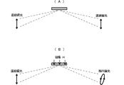
- FIG. 1 is a schematic diagram for explaining the measurement principle.
- the off-diagonal component ⁇ xy of the complex permittivity tensor ⁇ represented by the following equation is zero. As shown in FIG. 1A, this indicates that when linearly polarized light enters the sample, the reflected wave from the sample also becomes linearly polarized light.
- the reflected light contains only the p-polarized light component, and the incidence of linearly polarized light consisting of only the s-polarized component (s-polarized light incidence).
- the reflected wave includes only the s-polarized component.
- the off-diagonal component ⁇ xy of the complex dielectric constant tensor is not zero.
- the reflected wave from the sample becomes elliptically polarized light. That is, the reflected light includes not only the p-polarized component but also the s-polarized component with respect to the p-polarized incident, and the reflected wave includes not only the s-polarized component but also the p-polarized component with respect to the s-polarized incident. become.
- the complex detection is performed by detecting the p-polarized component and the s-polarized component contained in the reflected light when linearly polarized light is incident on the sample in a magnetic field applied state. It is possible to derive a diagonal component and a non-diagonal component of the dielectric constant tensor.
- the semiconductor sample is irradiated with pulsed light having a frequency component in the terahertz frequency range (0.1 ⁇ 10 12 to 100 ⁇ 10 12 hertz), and the intensity of the reflected light reflected by the sample and By detecting the phase difference, the material property value of the semiconductor sample is derived.
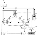
- FIG. 2 is a diagram showing the terahertz spectroscopy analyzer 1 according to the present embodiment.
- the terahertz spectrometer 1 includes a pulsed laser light source 2, a beam splitter 3, laser concentrators 4A and 4B, a terahertz light emitting module 5, parabolic mirrors 6A, 6B, 6C and 6D, polarizers 7A and 8A, and polarizer rotation. Stages 7B and 8B, magnet 9A, magnet drive stage 9B, terahertz detection module 10, probe light delay unit 11A, delay unit drive stage 11B, bias power supply 12, current amplifier 13, lock-in amplifier 14, control calculation unit 15, and stage A controller 16 is provided.
- the pulse laser light source 2 irradiates pulse laser light.
- the pulse width of the pulse laser beam is preferably 10 to 150 femtoseconds, and the light emission period is preferably several MHz.
- the beam splitter 3 guides the laser light emitted from the pulse laser light source 2 and splits the laser light into pump light and probe light.
- the laser concentrator 4A guides the pump light split by the beam splitter 3 and condenses the pump light.
- the probe light delay unit 11A guides the probe light dispersed by the beam splitter 3.
- the laser concentrator 4B condenses the probe light guided to the probe light delay unit 11A.
- FIG. 3 is a perspective view illustrating a detailed configuration of the terahertz light emitting module 5.
- the bias power source 12 applies a bias voltage to the terahertz light emitting module 5.
- the terahertz light emitting module 5 includes a photoconductive antenna element 5A and a silicon lens 5B.
- the photoconductive antenna element 5A includes a GaAs substrate 5C, a low temperature growth GaAs thin film 5D, and an antenna pattern electrode pair 5F having an antenna gap 5E.
- the low-temperature grown GaAs thin film 5D is formed on the surface of the GaAs substrate 5C.
- the antenna pattern electrode pair 5F is formed on the surface of the low-temperature grown GaAs thin film 5D.
- the antenna gap 5E is arranged at the focal position of the pump light L condensed by the laser concentrator 4A described above, and a bias voltage is applied from the bias power source 12.
- a bias voltage is applied from the bias power source 12.
- the silicon lens 5B is a hemispherical lens having a flat surface and a spherical surface, and is joined to the back surface of the GaAs substrate 5C by the flat surface, and radiates pulse light generated in the photoconductive antenna element 5A to free space.
- the terahertz light emitting module 5 emits pulsed light as substantially linearly polarized light.
- the terahertz light emitting module 5 is arranged in an attitude inclined by 45 ° from the reference arrangement angle at which the pulsed light substantially includes only the p-polarized component, whereby the pulsed light is substantially equal to the p-polarized component and the s-polarized component. To include the quantity.
- the parabolic mirrors 6A and 6C collimate the surface of the sample 50 with the pulsed light emitted from the terahertz light emitting module 5 into free space.
- the polarizer rotation stage 7B supports the polarizer 7A in a rotatable manner, and controls the rotation angle of the polarizer 7A by driving an actuator.
- the polarizer 7A is composed of, for example, a wire grid in which thin metal wires are periodically arranged.
- the front surface on which pulse light is incident and the rear surface on which pulse light is emitted are perpendicular to the rotation center, and the rotation center is a beam line of the pulse light. Arranged to coincide with the central axis.
- This polarizer 7A transmits only the polarization component along the specific direction determined according to its own rotation angle among the polarization components included in the incident pulsed light. Therefore, the polarizer 7A is tilted 45 ° from the reference arrangement angle at which the transmitted pulsed light includes only the p-polarized component, so that the emitted pulsed light includes equal amounts of the p-polarized component and the s-polarized component. It is configured to be rotatable up to the arrangement angle.
- the magnet drive stage 9B movably supports a magnet 9A for applying a magnetic field to the semiconductor sample 50, and controls the position of the magnet 9A by driving an actuator.
- the magnet 9A is disposed in the vicinity of the semiconductor sample 50 when a magnetic field is applied to the semiconductor sample 50, and is disposed in a position away from the vicinity of the semiconductor sample 50 when the application of the magnetic field to the semiconductor sample 50 is stopped.
- the magnetic field variable unit is configured by changing the distance between the permanent magnet and the sample is shown, but a configuration in which the magnetic field is turned ON / OFF using an electromagnet may be used.
- the pulsed light whose polarization state is controlled by the polarizer 7A is applied to the semiconductor sample 50 at a predetermined incident angle. If this incident angle is set to a so-called Brewster angle, high measurement sensitivity can be obtained, which is preferable.
- the pulsed light irradiated on the surface of the sample 50 is reflected by the influence of the complex dielectric constant tensor of the semiconductor sample 50. That is, as described with reference to FIG. 1, when linearly polarized light (p-polarized light incident) is incident on the semiconductor sample 50 in the non-magnetic field state, the reflected wave from the semiconductor sample 50 also becomes linearly polarized light (p-polarized light), and the semiconductor in the magnetic field applied state. When linearly polarized light is incident on the sample 50, the reflected wave from the semiconductor sample 50 becomes elliptically polarized light.
- the polarizer rotation stage 8B supports the polarizer 8A in a rotatable manner, and controls the rotation angle of the polarizer 8A by driving an actuator.
- the polarizer 8A is formed of a wire grid in which thin metal wires are periodically arranged.
- the front surface on which reflected light is incident and the rear surface on which reflected light is emitted are perpendicular to the rotation center, and the rotation center is a beam line of the reflected light. Arranged to coincide with the central axis.
- the polarizer 8A transmits only a polarized light component along a specific direction determined according to its rotation angle among polarized light components included in incident reflected light.
- the polarizer 8A can be rotated from a reference arrangement angle at which the reflected light to be transmitted contains only the p-polarized component to an arrangement angle inclined 90 ° at which the reflected light to be emitted contains only the s-polarized component.
- the parabolic mirror 6B guides the reflected light emitted from the polarizer 8A to the terahertz detection module 10.
- the delay unit drive stage 11B supports the probe light delay unit 11A so as to be movable, and controls the movement of the probe light delay unit 11A by driving the actuator.
- the probe light delay unit 11A expands and contracts the optical path length of the guided probe light by movement.
- the terahertz detection module 10 has substantially the same configuration as the terahertz light emitting module 5 shown in FIG. 3, for example.
- this terahertz detection module 10 the reflected light incident from the spherical surface of the silicon lens is guided to the photoconductive antenna element, whereby an electric field corresponding to the intensity of the reflected light is generated between the antenna gaps formed on the low-temperature grown GaAs thin film. To be applied.
- the probe light collected by the laser concentrator 4B is irradiated between the antenna gaps of the photoconductive antenna, a minute current corresponding to the electric field strength flows between the antenna gaps.
- the current amplifier 13 amplifies a minute current flowing between the antenna gaps of the terahertz detection module 10.
- the lock-in amplifier 14 controls the bias power source 12 so that the bias voltage is modulated at a predetermined period, and locks in a detection signal corresponding to the intensity of the reflected light from the output of the current amplifier 13 based on the modulation period of the bias voltage. To detect. As a result, the detection signal corresponding to the intensity of the reflected light is output to the control calculation unit 15 with an improved S / N ratio.
- the control calculation unit 15 outputs a control signal for scanning the delay unit driving stage 11B to the stage controller 16. Then, the stage controller 16 drives the actuator to move the probe light delay unit 11A. As a result, the arrival timing of the probe light is slightly shifted from the arrival timing of the reflected light periodically received by the terahertz detection module 10. Therefore, the detection timing of the weak current flowing between the antenna gaps is scanned with respect to the arrival timing of the reflected light, and the time waveform of the reflected light can be acquired.
- the probe light delay unit 11A, the delay unit drive stage 11B, and the terahertz detection module 10 constitute a waveform detection unit described in the claims.
- control calculation unit 15 outputs to the stage controller 16 a control signal for controlling either the magnetic field application state in which the magnetic field generated by the magnet 9A is applied to the semiconductor sample 50 or the no magnetic field state. Then, the stage controller 16 drives the actuator to move the magnet 9A. As a result, the semiconductor sample 50 enters either a magnetic field application state in which a magnetic field is applied by the magnet 9A or a no magnetic field state.
- the magnet 9A and the magnet drive stage 9B constitute the magnetic field variable unit described in the claims.
- control calculation unit 15 is a p-polarized incident state in which only the p-polarized component included in the pulsed light is transmitted through the polarizer 7A, or 45 ° polarized light that is equally transmitted through the p-polarized component and the s-polarized component included in the pulsed light.
- a control signal for controlling the incident state is output to the stage controller 16.
- the stage controller 16 drives the actuator to rotate the polarizer 7A.
- the polarizer 7A takes either the rotation angle at which the p-polarized light is incident or the rotation angle at which the 45-degree polarized light is incident by 45 ° from the rotation angle.
- control calculation unit 15 is either a p-polarized light emission state in which only the p-polarized light component included in the reflected light is transmitted through the polarizer 8A, or an s-polarized light emission state in which only the s-polarized light component included in the reflected light is transmitted.
- a control signal to be controlled is output to the stage controller 16.
- the stage controller 16 drives the actuator to rotate the polarizer 8A.
- the polarizer 8A takes either the rotation angle at which the p-polarized light is emitted or the rotation angle at which the s-polarized light is emitted by 90 ° from the rotation angle. Therefore, the control calculation unit 15 and the stage controller 16 constitute a control unit described in the claims.
- the terahertz spectroscopic analysis apparatus 1 having the above-described configuration is different from each other in the combination of a magnetic field application state or no magnetic field state, a p-polarized light incident state or a 45 ° polarized light incident state, a p-polarized light emission state or an s-polarized light emission state.
- the time waveform of 50 reflected lights can be automatically and continuously acquired by a program.
- the control calculation unit 15 derives the complex dielectric constant tensor and various material property values of the semiconductor sample 50 based on the time waveform of the reflected light detected by the above control.
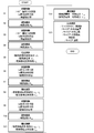
- FIG. 4 is a diagram illustrating an example of a processing flow of the control calculation unit 15.
- the control calculation unit 15 outputs a control signal that puts the polarizer 7A into a 45 ° polarized light incident state, outputs a control signal that puts the polarizer 8A into a p-polarized light emission state, and puts the magnet 9A into a non-magnetic field state. Is output (S1).
- the control calculation unit 15 outputs a control signal that instructs the probe light delay unit 11A to move a predetermined distance during a predetermined period.
- control calculation unit 15 outputs a control signal for setting the polarizer 8A to the s-polarized light emission state (S3). Then, the control calculation unit 15 outputs a control signal to the probe light delay unit 11A again, and irradiates the semiconductor sample 50 in the non-magnetic field state with linearly polarized light including equal amounts of the p-polarized component and the s-polarized component with the pulse light in the terahertz frequency band.
- the time waveform R S of the s-polarized component contained in the reflected light is detected (S4). Note that these steps (S3 to S4) correspond to the non-magnetic field measurement step recited in the claims.
- the control calculation unit 15 performs Fourier transform on the detected time waveform R p and time waveform R S , respectively, and derives an amplitude ratio spectrum and a phase difference spectrum of both, and from the amplitude ratio spectrum and the phase difference spectrum in a no magnetic field state.
- Such a method for deriving the complex dielectric constant using the amplitude reflection coefficient ratio of the p-polarized component and the s-polarized component is called an ellipsometry method. According to the ellipsometry method, reference measurement is unnecessary, and it is possible to prevent the occurrence of measurement errors due to the sample arrangement position deviation that easily occurs in the reference measurement.
- the process of deriving the complex amplitude reflection coefficient ratio using the ellipsometry method is generalized and described.
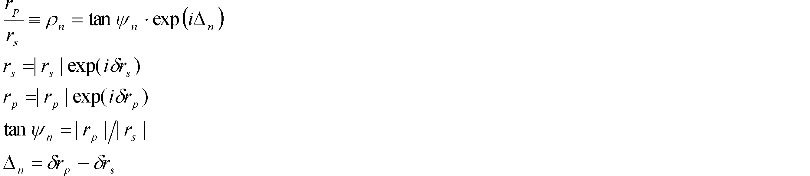
- the ratio ⁇ between the complex amplitude reflection coefficients r s and r p of both polarization components is obtained using the phase difference ⁇ n and the amplitude reflection coefficient ratio tan ⁇ n obtained from the amplitude ratio spectrum and the phase difference spectrum of the two polarization components.
- n is derived.
- the complex amplitude reflection coefficient ratio ⁇ n is expressed by the following equation.
- step S5 uses the phase difference ⁇ r and the amplitude reflection coefficient ratio tan ⁇ r obtained from the detected time waveform R p and time waveform R s. Is obtained by the equation (2).
- the complex dielectric constant ⁇ r in the semiconductor sample 50 in the non-magnetic field state is the incidence of pulsed light.
- the angle ⁇ i and the complex amplitude reflection coefficient ratio ⁇ r are represented by the following equations.
- the complex amplitude reflection coefficient r p is expressed by the following equation in which the incident angle theta i and the complex dielectric constant epsilon r a variable by using the Fresnel equations.
- control calculation unit 15 outputs a control signal for setting the polarizer 7A to the p-polarized light incident state, and outputs a control signal for setting the magnet 9A to the magnetic field application state (S6). Then, the control calculation unit 15 outputs a control signal to the probe light delay unit 11A, irradiates the semiconductor sample 50 in the magnetic field application state with the pulsed light in the terahertz frequency band as linearly polarized light including only the p-polarized component, and is included in the reflected light. The time waveform Rsp of the s-polarized component to be detected is detected (S7). These steps (S6 to S7) correspond to the magnetic field application measurement step described in the claims.
- the control calculation unit 15 Fourier-transforms the detected time waveform Rsp and the time waveform Rp , respectively, derives an amplitude ratio spectrum and a phase difference spectrum, and applies a magnetic field from the amplitude ratio spectrum and the phase difference spectrum.
- the complex amplitude reflection coefficient ratio in the semiconductor sample 50 in the state r sp / r p and derives the complex amplitude reflection coefficient r sp of s-polarized light emitted for p-polarized light incident on the magnetic field applied state (S8).
- the light intensity of the pulsed light is changed by changing the polarizer 7A from the 45 ° polarized light incident state to the p polarized light incident state. Therefore, in order to perform spectroscopic analysis with high accuracy, it is better to redetect the time waveform R p. desirable.
- the detection in the previous step S2 is used as it is.
- the complex amplitude reflection coefficient r sp the complex amplitude reflection coefficient ratio r sp / r p is derived by calculation, obtained by multiplying the complex amplitude reflection coefficient r p above.
- the control calculation unit 15 can derive the complex amplitude reflection coefficient r sp of the s-polarized light emission with respect to the p-polarized light incidence in the semiconductor sample 50 in the magnetic field application state.
- control calculation unit 15 outputs a control signal for setting the polarizer 8A to the p-polarized light emission state (S9). Then, the control calculation unit 15 outputs a control signal to the probe light delay unit 11A, irradiates the semiconductor sample 50 in the magnetic field application state with the pulsed light in the terahertz frequency band as linearly polarized light including only the p-polarized component, and is included in the reflected light. A time waveform R pp of the p-polarized component to be detected is detected (S10). Note that these steps (S9 to S10) correspond to the magnetic field application measurement step recited in the claims.
- the control calculation unit 15 Fourier transforms the detected time waveform R pp and the time waveform R p , derives the amplitude ratio spectrum and the phase difference spectrum, and applies a magnetic field from the amplitude ratio spectrum and the phase difference spectrum.
- the complex amplitude reflection coefficient ratio in the semiconductor sample 50 in the state r pp / r p and derives the complex amplitude reflection coefficient r pp of p-polarized light emitted for p-polarized light incident on the magnetic field applied state (S11). Since the light intensity of the output fluctuation and Shojire if pulse light of the pulse laser light source 2 is changed with time, the time waveform R p in order to perform spectroscopic analysis with high accuracy better to rediscover desirable .
- the detection in the previous step S2 is used as it is.
- the complex amplitude reflection coefficient r pp In the present embodiment, the complex amplitude reflection coefficient ratio r pp / r p is derived by calculation, obtained by multiplying the complex amplitude reflection coefficient r p above. Through the above derivation process, the control calculation unit 15 can derive the complex amplitude reflection coefficient r pp of p-polarized light emission with respect to p-polarized light incidence in the semiconductor sample 50 in the magnetic field application state.
- control calculation unit 15 performs the diagonal component ⁇ xx and the non-diagonal component of the complex permittivity tensor in the semiconductor sample 50 in the magnetic field application state based on the derived complex amplitude reflection coefficient r pp and complex amplitude reflection coefficient r sp.
- ⁇ xy is derived (S12).
- the previous derivation calculation steps (S5, S8, S11, S12) including this step (S12) correspond to the complex dielectric constant tensor derivation step described in the claims.
- the complex amplitude reflection coefficient r pp described above is expressed by the following equation using the Fresnel equation in the same manner as the equation 4 and using the diagonal component ⁇ xx of the complex permittivity tensor and the incident angle ⁇ i as variables.
- diagonal epsilon xx of the complex dielectric tensor can be derived using the complex amplitude reflection coefficient r pp.
- the number 7 expression by the following equation solving for the off-diagonal elements epsilon xy of the complex dielectric tensor can be derived non-diagonal components epsilon xy of the complex dielectric tensor.
- control calculation unit 15 based on the xy diagonal epsilon xx and off-diagonal components epsilon of the derived complex permittivity tensor, semiconductor samples with diagonal epsilon xx and off-diagonal elements epsilon xy as a parameter A material property value of 50 is derived (S13).
- This step (S13) corresponds to the material property value deriving step described in the claims.
- the cyclotron frequency ⁇ c is a frequency of cyclotron motion (circular motion) generated in a carrier when a magnetic field is applied to free carriers in the semiconductor.
- the diagonal and non-diagonal components ⁇ xx and ⁇ xy of the complex permittivity are given by the following equations using the cyclotron frequency ⁇ c as a variable, based on the Drude model in consideration of the magneto-optical effect.
- the high-frequency dielectric constant is ⁇ ⁇
- the plasma frequency is ⁇ p
- the angular frequency of the pulsed light is ⁇
- the carrier scattering probability is ⁇ .
- the plasma frequency ⁇ p is expressed by the following equation, where q is the unit charge, N is the carrier concentration, and ⁇ 0 is the vacuum dielectric constant.
- the cyclotron frequency ⁇ c can be derived from the following equation obtained by solving the equations (9) and (10).
- the effective mass m * of the carrier can be derived from the following equation based on the above-described cyclotron frequency ⁇ c .
- the complex electrical conductivity ⁇ can be derived from the following equation based on the Drude model using the complex dielectric constant ⁇ r in the absence of a magnetic field.
- the DC resistivity ⁇ is the real part of the reciprocal 1 / ⁇ of the complex electrical conductivity ⁇ and can be derived from the following equation.
- the complex electric conductivity ⁇ is expressed by the following equation based on Drude-Lorentz equation with the carrier scattering time ⁇ as a variable.
- the carrier scattering time ⁇ can be derived from the following equation based on the frequency (carrier scattering frequency) ⁇ ⁇ that is the intersection of the real part ⁇ ′ and the imaginary part ⁇ ′′.
- the carrier mobility ⁇ can be derived from the following equation.
- the carrier concentration N can be derived from the following equation.
- the complex permittivity ⁇ r in the non-magnetic field state, the diagonal component ⁇ xx and the off-diagonal component ⁇ xy of the complex permittivity tensor in the magnetic field applied state are derived.
- the material physical property values of various semiconductor samples 50 can be processed with simple equipment, without any parameter assumptions, and without any pretreatment. It can be derived without.
- a series of time waveforms can be detected and parameters can be derived automatically by using a program or the like, and even a person who does not have special technology or advanced knowledge can perform terahertz spectroscopy.
- the time waveform R p is measured a plurality of times, not once, before derivation of the complex amplitude reflection coefficient ratios r pp / r p and r sp / r p .
- an InAs wafer is used as a semiconductor sample, and effective mass, carrier concentration, mobility, and the like, which are material physical values, are derived.
- an n-type carrier type is used, and the material physical properties are about 0.02 ⁇ ⁇ cm according to the conventional hole measurement, and the carrier density is 3 ⁇ 10 16 cm ⁇ 3 or less. is there. Further, a neodymium magnet is used as the magnet, and the magnetic field strength is 0.46T.
- FIG. 5 is a diagram for explaining an example of the processing flow of the control arithmetic unit according to the present embodiment.
- the control calculation unit outputs a control signal to each unit, detects the time waveform R p of the p-polarized component contained in the reflected light in the non-magnetic state (S21 to S22), and s contained in the reflected light in the non-magnetic state.
- the time waveform R s of the polarization component is detected (S23 to S24).
- the complex amplitude reflection coefficient ratio ⁇ r , complex dielectric constant ⁇ r , and complex amplitude reflection coefficient r p of the InAs wafer in a non-magnetic field state are derived (S25).
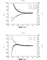
- FIG. 6 (A) is based on the complex dielectric constant epsilon r derived as example, a diagram illustrating the relationship between the real part epsilon 'and the imaginary part epsilon "the frequency of the complex dielectric constant epsilon r.
- the measurement zone in the low-frequency side, but the imaginary part decreases the real part of the complex dielectric constant epsilon r epsilon 'is epsilon "is increased, which indicates that the absorption by free carriers occurs at that frequency.
- control calculation unit outputs a control signal to each unit, detects a time waveform R sp of s-polarized light emission with respect to p-polarized light incident in a magnetic field application state (S26 to S27), and is included in the reflected light in a no magnetic field state. detecting a time waveform R p polarization components (S28 ⁇ S29).
- FIG. 7A is a diagram illustrating the relationship between the absolute value of reflectance of complex amplitude reflection coefficient r sp
- the reflectance is large near the center frequency of the measurement band, and the reflectance is small on the high frequency side and low frequency side of the measurement band. Further, the phase difference is small on the low frequency side of the measurement band, and the phase difference is large on the high frequency side.
- control calculation unit outputs a control signal to each unit, detects a time waveform R pp of p-polarized light emission with respect to p-polarized light incident in the magnetic field application state (S31 to S32), and is included in the reflected light in the non-magnetic field state. detecting a time waveform R p polarization components (S33 ⁇ S34).
- FIG. 7B is a diagram illustrating the relationship between the absolute value of reflectance of complex amplitude reflection coefficient r pp
- the reflectance is large on the low frequency side of the measurement band, and the reflectance is small on the high frequency side of the measurement band. Further, the phase difference is small on the low frequency side of the measurement band, and the phase difference is large on the high frequency side.
- control calculation unit based on the derived complex amplitude reflection coefficient r pp and complex amplitude reflection coefficient r sp , the diagonal component ⁇ xx and the non-diagonal component ⁇ xy of the complex dielectric constant tensor in the magnetic field applied InAs wafer. Is derived (S36). FIG.
- control calculation unit based on the diagonal epsilon xx and off-diagonal elements epsilon xy of the derived complex permittivity tensor of the semiconductor sample with a diagonal epsilon xx and off-diagonal elements epsilon xy as parameters material
- a physical property value is derived (S37).
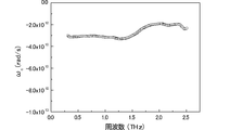
- Figure 9 is a diagram illustrating the frequency dependence of the cyclotron frequency omega c derived as examples.
- the average value of the cyclotron frequency ⁇ c at 0.5 to 1.5 THz was about ⁇ 3.1 ⁇ 10 12 rad / s.
- Sign of the derived cyclotron frequency omega c is negative, thereby determining the conductivity type of the sample is n-type.
- the conduction type of the semiconductor sample can be determined to be p-type.
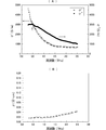
- FIG. 10A is a diagram illustrating the frequency dependence of the complex conductivity spectrum derived as an example. From the intersection of the real part ⁇ ′ and the imaginary part ⁇ “of the complex electrical conductivity ⁇ , it can be seen that the carrier scattering frequency ⁇ ⁇ is 0.5 THz. From this, the carrier scattering time ⁇ is 3 based on the equation (17). 2 ⁇ 10 ⁇ 13 s.
- FIG. 10B is a diagram illustrating the frequency dependence of the resistivity ⁇ derived as an example.
- the resistivity ⁇ can be derived as the reciprocal of the complex electrical conductivity ⁇ based on the equation (15), and it can be seen that the value of the DC resistivity ⁇ at a frequency of 0 Hz is 0.0175 ⁇ ⁇ cm. This value is almost consistent with the result of the conventional Hall measurement.
- the mobility ⁇ was 2.1 ⁇ 10 4 cm 2 / V ⁇ s from the equation (18). Further, when the carrier concentration N was derived as an example, the carrier concentration N was 1.6 ⁇ 10 16 cm ⁇ 3 from the equation (19). These values were on the same order as the results of the conventional Hall measurement.
- the value of the effective mass of the semiconductor can be directly evaluated without requiring special equipment in a room temperature environment.
- various material property values such as carrier concentration can be directly derived without using any assumed values, and various material property values can be derived with practical accuracy.
- SYMBOLS 1 Terahertz spectroscopy analyzer 2 ... Pulse laser light source 3 ... Beam splitter 4A, 4B ... Laser concentrator 5 ... Terahertz light emission module 5A ... Photoconductive antenna element 5B ... Silicon lens 5C ... GaAs substrate 5D ... Low temperature growth GaAs thin film 5E ... Antenna gap 5F ... Antenna pattern electrode pair 6A, 6B, 6C, 6D ... Parabolic mirrors 7A, 8A ... Polarizer 7B, 8B ... Polarizer rotation stage 9A ... Magnet 9B ... Magnet drive stage 10 ... Terahertz detection module 11A ... Probe Optical delay unit 11B ... Delay unit drive stage 12 ... Bias power supply 13 ... Current amplifier 14 ... Lock-in amplifier 15 ... Control operation unit 16 ... Stage controller 50 ... Semiconductor sample
Landscapes
- Physics & Mathematics (AREA)
- Spectroscopy & Molecular Physics (AREA)
- Health & Medical Sciences (AREA)
- Analytical Chemistry (AREA)
- Life Sciences & Earth Sciences (AREA)
- Chemical & Material Sciences (AREA)
- Toxicology (AREA)
- Biochemistry (AREA)
- General Health & Medical Sciences (AREA)
- General Physics & Mathematics (AREA)
- Immunology (AREA)
- Pathology (AREA)
- Investigating Or Analysing Materials By Optical Means (AREA)
Abstract
特殊な追加設備を用いずに、半導体の材料物性値を導出できるテラヘルツ分光分析方法を提供する。テラヘルツ分光分析方法では、磁場印加状態の試料に対してパルス光を照射し、試料に反射された反射波の時間波形Rsp,Rppを検出する(S6~S7,S9~S10)。また、無磁場状態の試料に対してパルス光を照射し、試料に反射された反射波の時間波形Rp,Rsを検出する(S1~S2,S3~S4)。また、時間波形Rp,Rs,Rsp,Rppに基づいて、試料の磁場印加状態での複素誘電率テンソルの対角成分εxxおよび非対角成分εxyを導出する(S5,S8,S11~S12)。そして、対角成分εxxおよび非対角成分εxyをパラメータに含む試料の材料物性値を導出する(S13)。
Description
この発明は、テラヘルツ光を用いて、試料の材料物性を分析するテラヘルツ分光分析装置、およびテラヘルツ分光分析方法に関するものである。
テラヘルツ周波数領域のパルス光を用いたテラヘルツ時間領域分光分析法では、フェムト秒オーダーのパルス幅でテラヘルツ周波数領域のパルス光を試料に照射し、試料で透過または反射した光の光応答特性から、試料の複素誘電率や電気伝導度を分析する。
半導体を試料とする場合、テラヘルツ光に対してフリーキャリアによるドルーデ型の吸収が生じる。このため、光応答特性からドルーデモデルを用いて半導体の各種材料物性値、例えば、キャリア濃度、移動度などを導出することが可能である(例えば非特許文献1参照)。半導体の材料物性値の測定に従来から用いられていたホール測定法では、半導体試料に電極形成を行う必要が有り、サンプル試料に対する測定しかできなかった。一方、テラヘルツ光の応答特性を用いるテラヘルツ分光分析では電極形成などの前プロセスが不要であり、半導体製品の材料本体を非接触、非破壊で試験することが可能になる。
ただし、非特許文献1のような従来の手法は、光応答特性を用いて分光分析を行うととともに、半導体キャリアの有効質量m*を推定する必要があった。具体的には、有効質量m*は、例えばGaAsを試料とする場合キャリア濃度によって変化するため、既知のキャリア濃度と有効質量m*との関係に基づいて最適なものを選択(フィッティング)し、用いていた。
なお、有効質量m*は、フォトルミネッセンス(PL)法を用いた測定方法(例えば非特許文献2参照)や、静磁場を印加した際にキャリアが加速される角回転速度、サイクロトロン周波数を測定し導出する方法(例えば非特許文献3、特に文献211~212頁参照)などにより、測定可能である。
P. G.Huggard, et.al.,"Drude conductivityof highlydoped GaAs at terahertz frequencies, Journal ofApplied Physics. 87,2382(2000).
D. M.Szmyd, et.al.,"Heavily doped GaAs:Se.I. Photoluminescence determination of the electroneffective mass, Journalof AppliedPhysics. 68,2367(1990).
キッテル固体物理学入門第8版,丸善,2005
既知のキャリア濃度と有効質量m*との関係に基づいて有効質量m*を仮定する非特許文献1の方法は、キャリア濃度と有効質量m*との関係が未知の材料に対して材料物性値を測定することが困難である。また、仮定した有効質量m*が実際の値から乖離して誤差が含まれることがある。
フォトルミネッセンス(PL)法を用いて有効質量m*を直接測定する非特許文献2の方法は、所謂バンド理論を熟知した者でなければ測定・解析が困難であり、テラヘルツ分光分析の設備とは別の特殊な追加設備で、PL測定を行う必要がある。
サイクロトロン周波数を用いて有効質量m*を直接測定する非特許文献3の方法は、エネルギー共鳴吸収を明確に観測する必要が有り、液体ヘリウムにより試料を冷却し、テスラオーダーの超強力磁石を用いて高磁場を発生させる必要がある。このためテラヘルツ分光分析の設備とは別の特殊な追加設備を要する。
本発明は、有効質量m*の仮定を用いずに、また簡易な設備で、半導体の材料物性値を導出できるテラヘルツ分光分析方法、および半導体の材料物性値の導出に係る様々な条件での光応答特性の検出を一括して行えるテラヘルツ分光分析装置の提供を目的とする。
請求項1に係る発明のテラヘルツ分光分析方法は、磁場印加測定ステップ、無磁場測定ステップ、複素誘電率テンソル導出ステップ、および材料物性値導出ステップを実施する。磁場印加測定ステップは、磁場印加状態の試料に対してテラヘルツ周波数領域のパルス光を照射し、前記試料にて反射された反射波の時間波形を検出するステップである。無磁場測定ステップは、無磁場状態の前記試料に対してテラヘルツ周波数領域のパルス光を照射し、前記試料にて反射された反射波の時間波形を検出するステップである。複素誘電率テンソル導出ステップは、前記磁場印加測定ステップおよび前記無磁場測定ステップで検出した時間波形に基づいて、前記試料の磁場印加状態での複素誘電率テンソルの対角成分および非対角成分を導出するステップである。材料物性値導出ステップは、前記複素誘電率テンソル導出ステップで導出した前記複素誘電率テンソルの対角成分および非対角成分をパラメータに含む試料の材料物性値を導出するステップである。
この方法で導出される複素誘電率テンソルの非対角成分は、無磁場状態では存在せず、磁気光学効果によって発生し、その誘電関数はサイクロトロン周波数を含むものとなる。前述のようにサイクロトン周波数は有効質量に依存するので、複素誘電率テンソルの非対角成分を測定することにより有効質量の値を直接求めることができる。この磁気光学効果を利用するために請求項1に係る発明は、試料に対して磁場印加状態と無磁場状態とでパルス光を照射して反射波の時間波形を測定する。このようにして測定した時間波形からは、複素誘電率テンソルの対角成分および非対角成分を導出できる。
従来は有効質量m*の仮定を用いて各種の材料物性値を導出していたが、請求項1に係る発明の分光分析方法では、有効質量m*の仮定を用いることなく、試料の各種材料物性値、例えばキャリアの移動度、抵抗率、キャリア濃度、キャリアの伝導型などを、複素誘電率テンソルの対角成分および非対角成分をパラメータとして導出することが可能になる。この一連の測定は、全て上述したテラヘルツ分光分析法により達成できるので、従来のホール測定に代表されるような電極形成を伴う破壊検査を行わずとも、非接触・非破壊で迅速な材料物性値の評価が可能になる。
従来は有効質量m*の仮定を用いて各種の材料物性値を導出していたが、請求項1に係る発明の分光分析方法では、有効質量m*の仮定を用いることなく、試料の各種材料物性値、例えばキャリアの移動度、抵抗率、キャリア濃度、キャリアの伝導型などを、複素誘電率テンソルの対角成分および非対角成分をパラメータとして導出することが可能になる。この一連の測定は、全て上述したテラヘルツ分光分析法により達成できるので、従来のホール測定に代表されるような電極形成を伴う破壊検査を行わずとも、非接触・非破壊で迅速な材料物性値の評価が可能になる。
請求項2に係る発明の磁場印加測定ステップは、p偏光入射に対する反射光に含まれるp偏光成分の時間波形(Rpp)、および、p偏光入射に対する反射光に含まれるs偏光成分の時間波形(Rsp)を検出するステップである。また、請求項2に係る発明の無磁場測定ステップは、反射光に含まれるp偏光成分の時間波形(Rp)、および、反射光に含まれるs偏光成分の時間波形(Rs)を検出するステップである。
これら4つの時間波形を検出することで、その他のパラメータの検出を行うことなく、複素誘電率テンソルの対角成分および非対角成分を導出できる。このため極めて容易に、複素誘電率テンソルの対角成分および非対角成分をパラメータとする試料の材料物性値を導出することが可能になる。
これら4つの時間波形を検出することで、その他のパラメータの検出を行うことなく、複素誘電率テンソルの対角成分および非対角成分を導出できる。このため極めて容易に、複素誘電率テンソルの対角成分および非対角成分をパラメータとする試料の材料物性値を導出することが可能になる。
請求項3に係る発明の複素誘電率テンソル導出ステップは、前記磁場印加測定ステップで検出するp偏光成分の時間波形(Rpp)および前記無磁場測定ステップで検出するp偏光成分の時間波形(Rp)に基づいて第一の複素振幅反射係数比(rpp/rp)を導出し、前記磁場印加測定ステップで検出するs偏光成分の時間波形(Rsp)および前記無磁場測定ステップで検出するp偏光成分の時間波形(Rp)に基づいて第二の複素振幅反射係数比(rsp/rp)を導出し、前記無磁場測定ステップで検出するp偏光成分の時間波形(Rp)およびs偏光成分の時間波形(Rs)に基づいて無磁場状態での試料の複素誘電率(εr)を導出し、前記複素誘電率(εr)に基づいて前記無磁場測定ステップで検出するp偏光成分の複素振幅反射係数(rp)を導出し、前記無磁場測定ステップで導出するp偏光成分の複素振幅反射係数(rp)、前記第一の複素振幅反射係数比(rpp/rp)、および前記第二の複素振幅反射係数比(rsp/rp)に基づいて、前記磁場印加測定ステップで検出するp偏光成分の複素振幅反射係数(rpp)およびs偏光成分の複素振幅反射係数(rsp)を導出し、前記磁場印加測定ステップで検出するp偏光成分の複素振幅反射係数(rpp)およびs偏光成分の複素振幅反射係数(rsp)に基づいて、磁場印加状態での試料の複素誘電率テンソルにおける対角成分(εxx)および非対角成分(εxy)を導出するステップである。
この構成では、p偏光成分の複素振幅反射係数(rpp)およびs偏光成分の複素振幅反射係数(rsp)の値を、各複素振幅反射係数比(rpp/rp,rsp/rp)から導出するので、誤差を生じやすいリファレンス測定が不要となり、高精度な分光分析が可能になる。
この構成では、p偏光成分の複素振幅反射係数(rpp)およびs偏光成分の複素振幅反射係数(rsp)の値を、各複素振幅反射係数比(rpp/rp,rsp/rp)から導出するので、誤差を生じやすいリファレンス測定が不要となり、高精度な分光分析が可能になる。
請求項4に係る発明の無磁場測定ステップは、p偏光成分の時間波形(Rp)の検出を、各時間波形(Rs、Rpp、Rsp)それぞれの検出を行う度に実施するステップである。
これにより、時間波形の検出中に試料への入射光強度が変動するようなことがあっても、短い時間隔で検出された2つの時間波形に基づいて、各複素振幅反射係数比(rpp/rp,rsp/rp)を導出できる。したがって、測定結果に対する試料への入射光強度の変動の影響を小さくでき、高精度な分光分析が可能になる。
これにより、時間波形の検出中に試料への入射光強度が変動するようなことがあっても、短い時間隔で検出された2つの時間波形に基づいて、各複素振幅反射係数比(rpp/rp,rsp/rp)を導出できる。したがって、測定結果に対する試料への入射光強度の変動の影響を小さくでき、高精度な分光分析が可能になる。
請求項11に係る発明のテラヘルツ分光分析装置は、第一の偏光子、第二の偏光子、波形検出部、磁場可変部、および制御部を備え、上述のテラヘルツ分光分析方法を実施する装置である。第一の偏光子は、前記パルス光をp偏光成分のみの第一の偏光状態またはp偏光成分とs偏光成分とを含む第二の偏光状態の少なくともいずれかに偏光する。第二の偏光子は、前記反射波をp偏光成分のみの第一の偏光状態またはs偏光成分のみの第二の偏光状態の少なくともいずれかに偏光する。波形検出部は、前記第二の偏光子で偏光された前記反射波の時間波形を検出する。磁場可変部は、前記試料に対して発生磁場を印加する磁場印加状態または無磁場状態を可変とさせることができる。制御部は、前記第一の偏光子と前記第二の偏光子と前記磁場可変部との状態組み合わせを変更して、前記波形検出部に前記反射光の時間波形を複数回検出させる。
この構成では、試料を固定したままの状態で一括して各時間波形を検出でき、高精度な分光分析が行える。
この構成では、試料を固定したままの状態で一括して各時間波形を検出でき、高精度な分光分析が行える。
請求項12に係る発明の制御部は、波形検出部に制御信号を出力し、波形検出部は、制御信号に応じて、プローブ光の光路長を変更するように駆動し、ポンプ光により発生させたパルス光の反射光に対して、プローブ光を用いて時間波形を検出すると好適である。
請求項13に係る発明の制御部は、第一の偏光子と第二の偏光子と磁場可変部とのそれぞれに制御信号を出力し、第一の偏光子および第二の偏光子は制御信号に応じて回転駆動し、磁場可変部は制御信号に応じて試料に印加する磁場強度を可変とする。また、請求項14に係る磁場可変部は、制御信号に応じて試料と磁石との間隔を変更するように駆動する機構により構成できる。
これらの構成により、この装置で一連の測定操作を、連続的に自動化して行うことが可能になる。
これらの構成により、この装置で一連の測定操作を、連続的に自動化して行うことが可能になる。
請求項15に係る発明の第一の偏光子は、前記パルス光を第一の偏光状態に偏光する回転角から、前記パルス光を第二の偏光状態に偏光する回転角まで、少なくとも45°回転駆動すると好適である。
また、請求項16に係る発明の第二の偏光子は、前記反射光を第一の偏光状態に偏光する回転角から、前記反射光を第二の偏光状態に偏光する回転角まで、少なくとも90°回転駆動すると好適である。
これらの構成により、テラヘルツ光の偏光状態の一連の制御を、自動化して行うことが可能になる。
また、請求項16に係る発明の第二の偏光子は、前記反射光を第一の偏光状態に偏光する回転角から、前記反射光を第二の偏光状態に偏光する回転角まで、少なくとも90°回転駆動すると好適である。
これらの構成により、テラヘルツ光の偏光状態の一連の制御を、自動化して行うことが可能になる。
この発明によれば、試料に対して磁場印加状態と無磁場状態とでパルス光を照射して反射波の時間波形を検出することで、特殊な追加設備を用いることなく、検出した時間波形から複素誘電率テンソルの対角成分および非対角成分を導出できる。このため、簡易な設備で、有効質量m*の仮定を行うことなく、また試料に一切の前処理を施すことなく、複素誘電率テンソルの対角成分および非対角成分をパラメータとする試料の材料物性値を直接導出することが可能になる。これらの一連の測定およびパラメータの導出は、プログラム等を用いて全自動で行うことが可能であり、このため特殊な技術や高度な知識を有していない者でもテラヘルツ分光分析を実施することが可能になる。
まず、本発明での磁気光学効果を利用した複素誘電率テンソルの測定原理に付いて説明する。図1は、その測定原理を説明する模式図である。
磁場が印加されていない無磁場状態の試料では、次式に示す複素誘電率テンソルεの非対角成分εxyがゼロとなる。このことは、図1(A)に示すように、試料に直線偏光が入射すると試料からの反射波も直線偏光となることを示している。即ち、p偏光成分のみからなる直線偏光の入射(p偏光入射)に対しては反射光がp偏光成分のみを含むことになり、s偏光成分のみからなる直線偏光の入射(s偏光入射)に対しては反射波がs偏光成分のみを含むことになる。
磁場が印加されていない無磁場状態の試料では、次式に示す複素誘電率テンソルεの非対角成分εxyがゼロとなる。このことは、図1(A)に示すように、試料に直線偏光が入射すると試料からの反射波も直線偏光となることを示している。即ち、p偏光成分のみからなる直線偏光の入射(p偏光入射)に対しては反射光がp偏光成分のみを含むことになり、s偏光成分のみからなる直線偏光の入射(s偏光入射)に対しては反射波がs偏光成分のみを含むことになる。

一方、磁場が印加されている磁場印加状態の試料では、その複素誘電率テンソルの非対角成分εxyがゼロではなくなる。このことは、図1(B)に示すように、試料に直線偏光が入射すると試料からの反射波は楕円偏光となることを示している。即ち、p偏光入射に対して反射光がp偏光成分のみでなくs偏光成分をも含むことになり、s偏光入射に対しては反射波がs偏光成分のみでなくp偏光成分をも含むことになる。
したがって、複素誘電率テンソルの導出過程の詳細は後述するが、磁場印加状態で直線偏光を試料に入射させた場合の反射光に含まれるp偏光成分およびs偏光成分をそれぞれ検出することで、複素誘電率テンソルの対角成分および非対角成分の導出が可能になる。
《第1の実施形態》
以下、本発明の実施形態に係るテラヘルツ分光分析方法を実施するテラヘルツ分光分析装置の構成例を説明する。本実施形態のテラヘルツ分光分析方法では、テラヘルツ周波数領域(0.1×10¹²~100×1012ヘルツ)の周波数成分を有するパルス光を半導体試料に照射し、試料で反射した反射光の強度および位相差を検出することにより、半導体試料の材料物性値を導出する。
以下、本発明の実施形態に係るテラヘルツ分光分析方法を実施するテラヘルツ分光分析装置の構成例を説明する。本実施形態のテラヘルツ分光分析方法では、テラヘルツ周波数領域(0.1×10¹²~100×1012ヘルツ)の周波数成分を有するパルス光を半導体試料に照射し、試料で反射した反射光の強度および位相差を検出することにより、半導体試料の材料物性値を導出する。
図2は、本実施形態に係るテラヘルツ分光分析装置1を示す図である。テラヘルツ分光分析装置1は、パルスレーザ光源2、ビームスプリッタ3、レーザ集光器4A,4B、テラヘルツ発光モジュール5、放物面鏡6A,6B,6C,6D、偏光子7A,8A、偏光子回転ステージ7B,8B、磁石9A、磁石駆動ステージ9B、テラヘルツ検出モジュール10、プローブ光遅延部11A、遅延部駆動ステージ11B、バイアス電源12、カレントアンプ13、ロックインアンプ14、制御演算部15、およびステージコントローラ16を備える。
パルスレーザ光源2は、パルスレーザ光を照射する。パルスレーザ光のパルス幅は10~150フェムト秒が望ましく、発光周期は数MHzが望ましい。ビームスプリッタ3は、パルスレーザ光源2から照射されたレーザ光が導光され、そのレーザ光をポンプ光およびプローブ光に分光する。レーザ集光器4Aはビームスプリッタ3で分光されたポンプ光が導光され、そのポンプ光を集光する。プローブ光遅延部11Aはビームスプリッタ3で分光されたプローブ光を導光する。レーザ集光器4Bはプローブ光遅延部11Aに導光されたプローブ光を集光する。
図3はテラヘルツ発光モジュール5の詳細構成を説明する斜視図である。バイアス電源12は、テラヘルツ発光モジュール5にバイアス電圧を印加する。テラヘルツ発光モジュール5は、光伝導アンテナ素子5Aとシリコンレンズ5Bとからなり、光伝導アンテナ素子5AはGaAs基板5Cと低温成長GaAs薄膜5Dとアンテナギャップ5Eを有するアンテナパターン電極対5Fとを備える。低温成長GaAs薄膜5DはGaAs基板5Cの表面に成膜されている。アンテナパターン電極対5Fは、低温成長GaAs薄膜5Dの表面に形成されている。アンテナギャップ5Eは、前述のレーザ集光器4Aで集光されるポンプ光Lの焦点位置に配置され、バイアス電源12からバイアス電圧が印加される。アンテナギャップ5Eにポンプ光Lがフェムト秒単位のパルス幅で照射されることで、低温成長GaAs薄膜5Dで光励起キャリアが発生して、アンテナギャップ5Eに電流が瞬間的に流れる。すると電気双極子放射によってテラヘルツ周波数成分を持ったパルス光が発生する。このパルス光は、アンテナギャップ5Eの電極対向方向に沿った偏光方向を持ち、パルス幅がフェムト秒オーダーである。シリコンレンズ5Bは、平坦面と球状面とを有する半球状のレンズであり、平坦面でGaAs基板5Cの背面に接合され、光伝導アンテナ素子5Aにおいて発生したパルス光を自由空間に放射する。シリコンレンズ5Bを設けることで、GaAs基板5Cとシリコンレンズ5Bとの界面における反射を抑えて、パルス光を自由空間に放射することができる。なお、このテラヘルツ発光モジュール5は、ほぼ直線偏光としてパルス光を放射することになる。そこでテラヘルツ発光モジュール5を、パルス光がほぼp偏光成分のみを含むことになる基準配置角度から45°傾けた姿勢で配置し、これにより、パルス光がp偏光成分とs偏光成分とをほぼ等量含むようにする。
再び図2に基づいて各部の構成を説明する。放物面鏡6A,6Cは、テラヘルツ発光モジュール5から自由空間に放射されたパルス光を試料50の表面にコリメートする。偏光子回転ステージ7Bは偏光子7Aを回転可能に支持し、アクチュエータの駆動により偏光子7Aの回転角を制御する。偏光子7Aは、例えば金属細線を周期的に配列したワイヤーグリッドで構成し、パルス光が入射する正面およびパルス光を出射する背面が回転中心に対して垂直で、回転中心がパルス光のビームライン中心軸と一致するように配置される。この偏光子7Aは、入射するパルス光に含まれる偏光成分のうち、自らの回転角に応じて定まる特定方向に沿った偏光成分のみを透過する。そこで、偏光子7Aは、透過するパルス光がp偏光成分のみを含むことになる基準配置角度から、出射するパルス光がp偏光成分とs偏光成分とを等量含むことになる45°傾けた配置角度まで回転可能に構成する。
磁石駆動ステージ9Bは、半導体試料50に磁場を印加するための磁石9Aを移動可能に支持し、アクチュエータの駆動により磁石9Aの位置を制御する。磁石9Aは、半導体試料50に磁場を印加する場合に半導体試料50の近傍に配置され、半導体試料50への磁場の印加を中止する場合に、半導体試料50の近傍から離れた位置に配置される。なお、本実施例では、磁場可変部を永久磁石と試料の距離を変えることによって構成する例を示すが、電磁石を用いて磁場のON/OFFを切り替える構成であっても良い。
偏光子7Aによって偏光状態が制御されたパルス光は、半導体試料50に所定の入射角で照射される。この入射角は、いわゆるブリュースター角に設定されていると高い測定感度を得ることが可能になり好適である。試料50の表面に照射されたパルス光は、半導体試料50の持つ複素誘電率テンソルによる影響を受けて反射する。即ち、図1にて説明したように、無磁場状態の半導体試料50に直線偏光(p偏光入射)が入射すると半導体試料50からの反射波も直線偏光(p偏光)となり、磁場印加状態の半導体試料50に直線偏光が入射すると半導体試料50からの反射波は楕円偏光となる。
偏光子回転ステージ8Bは偏光子8Aを回転可能に支持し、アクチュエータの駆動により偏光子8Aの回転角を制御する。偏光子8Aは、例えば金属細線を周期的に配列したワイヤーグリッドで構成し、反射光が入射する正面および反射光を出射する背面が回転中心に対して垂直で、回転中心が反射光のビームライン中心軸と一致するように配置される。この偏光子8Aは、入射する反射光に含まれる偏光成分のうち、自らの回転角に応じて定まる特定方向に沿った偏光成分のみを透過する。そこで、偏光子8Aは、透過する反射光がp偏光成分のみを含むことになる基準配置角度から、出射する反射光がs偏光成分のみを含むことになる90°傾けた配置角度まで回転可能に構成する。放物面鏡6Bは、偏光子8Aから出射された反射光をテラヘルツ検出モジュール10に導光する。
遅延部駆動ステージ11Bは、プローブ光遅延部11Aを移動可能に支持し、アクチュエータの駆動によりプローブ光遅延部11Aの移動を制御する。プローブ光遅延部11Aは、導光するプローブ光の光路長を移動により伸縮させる。
テラヘルツ検出モジュール10は、例えば図3に示したテラヘルツ発光モジュール5と略同じ構成である。このテラヘルツ検出モジュール10では、シリコンレンズの球状面から入射する反射光を光伝導アンテナ素子に導光することで、反射光の強度に応じた電界を低温成長GaAs薄膜上に形成されたアンテナギャップ間に印加させる。レーザ集光器4Bで集光されたプローブ光が光伝導アンテナのアンテナギャップ間に照射される時、電界強度に応じた微少電流がアンテナギャップ間に流れる。
カレントアンプ13は、テラヘルツ検出モジュール10のアンテナギャップ間に流れる微少電流を増幅する。ロックインアンプ14はバイアス電圧が所定の周期で変調するようにバイアス電源12を制御し、バイアス電圧の変調周期に基づいてカレントアンプ13の出力から、反射光の強度に応じた検出信号をロックイン検出する。これにより、反射光の強度に応じた検出信号をS/N比を改善して制御演算部15に出力する。
制御演算部15は、遅延部駆動ステージ11Bを走査する制御信号をステージコントローラ16に出力する。するとステージコントローラ16はアクチュエータを駆動して、プローブ光遅延部11Aを移動させる。これによりテラヘルツ検出モジュール10において周期的に受光する反射光の到達タイミングに対して、プローブ光の到達タイミングが微小時間ずつずれる。したがって、アンテナギャップ間に流れる微弱電流の検出タイミングが反射光の到達タイミングに対して走査され、反射光の時間波形を取得することが可能になる。なお、プローブ光遅延部11A、遅延部駆動ステージ11B、およびテラヘルツ検出モジュール10は請求項に記載の波形検出部を構成する。
また制御演算部15は、半導体試料50に磁石9Aの発生磁場を印加する磁場印加状態または無磁場状態のいずれかに制御する制御信号をステージコントローラ16に出力する。するとステージコントローラ16はアクチュエータを駆動して、磁石9Aを移動させる。これにより、半導体試料50は磁石9Aによる磁場が印加される磁場印加状態または無磁場状態のいずれかになる。なお、磁石9A、および磁石駆動ステージ9Bは請求項に記載の磁場可変部を構成する。
また制御演算部15は、偏光子7Aをパルス光に含まれるp偏光成分のみを透過するp偏光入射状態、または、パルス光に含まれるp偏光成分およびs偏光成分を等量透過する45°偏光入射状態、のいずれかに制御する制御信号をステージコントローラ16に出力する。するとステージコントローラ16はアクチュエータを駆動して、偏光子7Aを回転させる。これにより、偏光子7Aは、p偏光入射状態になる回転角、または、その回転角から45°回転した45°偏光入射状態になる回転角のいずれかの姿勢をとる。
また制御演算部15は、偏光子8Aを反射光に含まれるp偏光成分のみを透過するp偏光出射状態、または、反射光に含まれるs偏光成分のみを透過するs偏光出射状態、のいずれかに制御する制御信号をステージコントローラ16に出力する。するとステージコントローラ16はアクチュエータを駆動して、偏光子8Aを回転させる。これにより、偏光子8Aは、p偏光出射状態になる回転角、または、その回転角から90°回転したs偏光出射状態になる回転角のいずれかの姿勢をとる。したがって制御演算部15およびステージコントローラ16は請求項に記載の制御部を構成する。
以上の構成のテラヘルツ分光分析装置1は、磁場印加状態または無磁場状態、p偏光入射状態または45°偏光入射状態、p偏光出射状態またはs偏光出射状態、それぞれの組み合わせを異ならせて、半導体試料50の反射光の時間波形をプログラムにより自動的に連続して取得することが可能となる。
制御演算部15は上述の制御により検出する反射光の時間波形に基づいて、半導体試料50の複素誘電率テンソル、および各種材料物性値を導出する。図4は、制御演算部15の処理フローの一例を説明する図である。
まず制御演算部15は、偏光子7Aを45°偏光入射状態にする制御信号を出力し、偏光子8Aをp偏光出射状態にする制御信号を出力し、磁石9Aを無磁場状態にする制御信号を出力する(S1)。そして制御演算部15は、プローブ光遅延部11Aに所定期間に所定距離移動するように指示する制御信号を出力する。これにより、テラヘルツ周波数帯域のパルス光をp偏光成分およびs偏光成分を等量含む直線偏光として無磁場状態の半導体試料50に照射させ、反射光に含まれるp偏光成分の時間波形Rpを検出する(S2)。なお、これらのステップ(S1~S2)は請求項に記載の無磁場測定ステップに相当する。
まず制御演算部15は、偏光子7Aを45°偏光入射状態にする制御信号を出力し、偏光子8Aをp偏光出射状態にする制御信号を出力し、磁石9Aを無磁場状態にする制御信号を出力する(S1)。そして制御演算部15は、プローブ光遅延部11Aに所定期間に所定距離移動するように指示する制御信号を出力する。これにより、テラヘルツ周波数帯域のパルス光をp偏光成分およびs偏光成分を等量含む直線偏光として無磁場状態の半導体試料50に照射させ、反射光に含まれるp偏光成分の時間波形Rpを検出する(S2)。なお、これらのステップ(S1~S2)は請求項に記載の無磁場測定ステップに相当する。
次に制御演算部15は、偏光子8Aをs偏光出射状態にする制御信号を出力する(S3)。そして制御演算部15は、再びプローブ光遅延部11Aに制御信号を出力し、テラヘルツ周波数帯域のパルス光をp偏光成分およびs偏光成分を等量含む直線偏光として無磁場状態の半導体試料50に照射させ、反射光に含まれるs偏光成分の時間波形RSを検出する(S4)。なお、これらのステップ(S3~S4)は請求項に記載の無磁場測定ステップに相当する。
次に制御演算部15は、検出した時間波形Rpおよび時間波形RSをそれぞれフーリエ変換し、両者の振幅比スペクトルおよび位相差スペクトルを導出し、振幅比スペクトルおよび位相差スペクトルから無磁場状態での半導体試料50の振幅反射係数比ρr、複素誘電率εr、および、p偏光成分の複素振幅反射係数rpを導出する(S5)。このようなp偏光成分とs偏光成分との振幅反射係数比を用いる複素誘電率の導出法はエリプソメトリ法と呼ばれる。エリプソメトリ法によれば、リファレンス測定が不要であり、リファレンス測定において生じやすい試料の配置位置ずれに伴う測定誤差の発生を防げる。
ここで、エリプソメトリ法を用いた複素振幅反射係数比の導出過程を一般化して説明する。エリプソメトリ法では2つの偏光成分の振幅比スペクトルおよび位相差スペクトルから得られる位相差Δnおよび振幅反射係数比tanΨnを用いて、両偏光成分の複素振幅反射係数rs,rpの比ρnを導出する。複素振幅反射係数比ρnは次式で表される。なお複素振幅反射係数rs及びrpの極座標表示での反射率をそれぞれ|rs|,|rp|、位相をδrs,δrpとする。
したがって、ステップS5での本実施形態に係る複素振幅反射係数比ρrの導出は、検出する時間波形Rpと時間波形Rsとから得られる位相差Δrおよび振幅反射係数比tanΨrを用いて、数2の式によって得られる。
前式で導出する複素振幅反射係数比ρrについて、試料表面における反射のみを考慮して、いわゆるフレネルの式を適用すると、無磁場状態の半導体試料50における複素誘電率εrはパルス光の入射角θiと複素振幅反射係数比ρrとを変数とした次式で表される。

また、複素振幅反射係数rpはフレネルの式を用いることで入射角θiと複素誘電率εrとを変数とした次式で表される。

以上の導出過程を経て、制御演算部15では無磁場状態の半導体試料50における複素誘電率εrおよびp偏光入射成分に対する複素振幅反射係数rpを導出できる。
次に制御演算部15は、偏光子7Aをp偏光入射状態にする制御信号を出力し、磁石9Aを磁場印加状態にする制御信号を出力する(S6)。そして制御演算部15は、プローブ光遅延部11Aに制御信号を出力し、テラヘルツ周波数帯域のパルス光をp偏光成分のみを含む直線偏光として磁場印加状態の半導体試料50に照射させ、反射光に含まれるs偏光成分の時間波形Rspを検出する(S7)。なお、これらのステップ(S6~S7)は請求項に記載の磁場印加測定ステップに相当する。
次に制御演算部15は、検出した時間波形Rspおよび前記時間波形Rpをそれぞれフーリエ変換し、両者の振幅比スペクトルおよび位相差スペクトルを導出し、振幅比スペクトルおよび位相差スペクトルから、磁場印加状態の半導体試料50における複素振幅反射係数比rsp/rpおよび、磁場印加状態でのp偏光入射に対するs偏光出射の複素振幅反射係数rspを導出する(S8)。なお、偏光子7Aを45°偏光入射状態からp偏光入射状態に変更することでパルス光の光強度が変化するため、分光分析を高精度に行うためには時間波形Rpは再検出するほうが望ましい。ここでは説明の簡易化のために、先のステップS2で検出するものをそのまま用いることとする。
ここで、複素振幅反射係数rspは、演算によって導出する複素振幅反射係数比rsp/rpに、前述の複素振幅反射係数rpを乗じることによって得る。
以上の導出過程を経て、制御演算部15では磁場印加状態の半導体試料50におけるp偏光入射に対するs偏光出射の複素振幅反射係数rspを導出できる。
以上の導出過程を経て、制御演算部15では磁場印加状態の半導体試料50におけるp偏光入射に対するs偏光出射の複素振幅反射係数rspを導出できる。
次に制御演算部15は、偏光子8Aをp偏光出射状態にする制御信号を出力する(S9)。そして制御演算部15は、プローブ光遅延部11Aに制御信号を出力し、テラヘルツ周波数帯域のパルス光をp偏光成分のみを含む直線偏光として磁場印加状態の半導体試料50に照射させ、反射光に含まれるp偏光成分の時間波形Rppを検出する(S10)。なお、これらのステップ(S9~S10)は請求項に記載の磁場印加測定ステップに相当する。
次に制御演算部15は、検出した時間波形Rppおよび前記時間波形Rpをそれぞれフーリエ変換し、両者の振幅比スペクトルおよび位相差スペクトルを導出し、振幅比スペクトルおよび位相差スペクトルから、磁場印加状態の半導体試料50における複素振幅反射係数比rpp/rpおよび、磁場印加状態でのp偏光入射に対するp偏光出射の複素振幅反射係数rppを導出する(S11)。なお、時間の経過に伴ってパルスレーザ光源2の出力変動などが生じればパルス光の光強度が変化するため、分光分析を高精度に行うためには時間波形Rpは再検出するほうが望ましい。ここでは説明の簡易化のために、先のステップS2で検出するものをそのまま用いることとする。
ここで、本実施形態において複素振幅反射係数rppは、演算によって導出する複素振幅反射係数比rpp/rpに、前述の複素振幅反射係数rpを乗じることによって得る。
以上の導出過程を経て、制御演算部15では磁場印加状態の半導体試料50におけるp偏光入射に対するp偏光出射の複素振幅反射係数rppを導出できる。
以上の導出過程を経て、制御演算部15では磁場印加状態の半導体試料50におけるp偏光入射に対するp偏光出射の複素振幅反射係数rppを導出できる。
次に、制御演算部15は、導出した複素振幅反射係数rppおよび複素振幅反射係数rspに基づいて磁場印加状態の半導体試料50における複素誘電率テンソルの対角成分εxxおよび非対角成分εxyを導出する(S12)。なお、このステップ(S12)を含むこれ以前の導出演算ステップ(S5,S8,S11,S12)は請求項に記載の複素誘電率テンソル導出ステップに相当する。
ここで、複素誘電率テンソルの対角成分εxxおよび非対角成分εxyの導出過程の詳細を説明する。前述の複素振幅反射係数rppは、数4の式と同様にフレネルの式を適用して、複素誘電率テンソルの対角成分εxxと入射角θiとを変数とした次式で表される。

数5の式を複素誘電率テンソルの対角成分εxxについて解くと、複素誘電率テンソルの対角成分εxxは複素振幅反射係数rppを用いて導出できる。

同様にして前述の複素振幅反射係数rspは、マクスウェルの式およびフレネルの式を適用して次式で表される。

数7の式を複素誘電率テンソルの非対角成分εxyについて解いた次式によって、複素誘電率テンソルの非対角成分εxyを導出できる。

次に、制御演算部15は、導出した複素誘電率テンソルの対角成分εxxおよび非対角成分εxyに基づいて、対角成分εxxおよび非対角成分εxyをパラメータとしてもつ半導体試料50の材料物性値を導出する(S13)。なお、このステップ(S13)は請求項に記載の材料物性値導出ステップに相当する。
ここで、半導体試料50の材料物性値導出過程の詳細を説明する。
サイクロトロン周波数ωcとは、半導体中のフリーキャリアに磁場を印加することで、キャリアに生じるサイクロトロン運動(円運動)の周波数である。
複素誘電率の対角・非対角成分εxx、εxyは、磁気光学効果を考慮したドルーデモデルに基づくと、それぞれサイクロトロン周波数ωcを変数とする次式で与えられる。なお、高周波誘電率をε∞、プラズマ周波数をωp、パルス光の角周波数をω、キャリアの散乱確率をγとする。
サイクロトロン周波数ωcとは、半導体中のフリーキャリアに磁場を印加することで、キャリアに生じるサイクロトロン運動(円運動)の周波数である。
複素誘電率の対角・非対角成分εxx、εxyは、磁気光学効果を考慮したドルーデモデルに基づくと、それぞれサイクロトロン周波数ωcを変数とする次式で与えられる。なお、高周波誘電率をε∞、プラズマ周波数をωp、パルス光の角周波数をω、キャリアの散乱確率をγとする。


なお、プラズマ周波数ωpは、単位電荷量をq、キャリア濃度をN、真空の誘電率をε0として次式で表される。

したがって、サイクロトロン周波数ωcは、上記数9,10の式を解いた次式によって導出できる。

またキャリアの有効質量m*は、前述のサイクロトロン周波数ωcに基づいて、次式によって導出できる。

また複素電気伝導度σは無磁場での複素誘電率εrを用いて、ドルーデモデルに基づく次式によって導出できる。

また直流抵抗率ρは、複素電気伝導度σの逆数1/σの実部であり、次式によって導出できる。

また複素電気伝導度σはキャリアの散乱時間τを変数として、ドルーデ・ローレンツの式に基づく次式で表される。

またキャリアの散乱時間τは、実部σ‘と虚部σ“の交点となる周波数(キャリアの散乱頻度)ωτに基づいて、次式によって導出できる。

またキャリアの移動度μは、次式によって導出できる。

またキャリア濃度Nは、次式によって導出できる。

従って、本実施形態のテラヘルツ分光分析方法によれば、無磁場状態での複素誘電率εr、磁場印加状態での複素誘電率テンソルの対角成分εxxおよび非対角成分εxyを導出し、その対角成分および非対角成分をパラメータに用いることで、様々な半導体試料50の材料物性値を簡易な設備で、パラメータの仮定を行うことなく、また試料に一切の前処理を施すことなく導出できる。そのための一連の時間波形の検出および各パラメータの導出を、プログラム等を用いて全自動で行え、特殊な技術や高度な知識を有していない者でもテラヘルツ分光分析を実施することができる。
《第2の実施形態》
次に、本発明の第2の実施形態に係るテラヘルツ分光分析方法に付いて説明する。本実施形態では、時間波形Rpの測定を一回ではなく複数回、複素振幅反射係数比rpp/rp,rsp/rpそれぞれの導出前にも実施する。また、半導体試料としてInAsウェハを用い、その材料物性値である有効質量、キャリア濃度、移動度などの導出を行う。なお、InAsウェハとしては、キャリアタイプがn型のものを用い、その材料物性値は、従来のホール測定による抵抗率が約0.02Ω・cm、キャリア密度が3×1016cm-3以下である。また、磁石にはネオジウム磁石を用い、磁場強度は0.46Tである。
次に、本発明の第2の実施形態に係るテラヘルツ分光分析方法に付いて説明する。本実施形態では、時間波形Rpの測定を一回ではなく複数回、複素振幅反射係数比rpp/rp,rsp/rpそれぞれの導出前にも実施する。また、半導体試料としてInAsウェハを用い、その材料物性値である有効質量、キャリア濃度、移動度などの導出を行う。なお、InAsウェハとしては、キャリアタイプがn型のものを用い、その材料物性値は、従来のホール測定による抵抗率が約0.02Ω・cm、キャリア密度が3×1016cm-3以下である。また、磁石にはネオジウム磁石を用い、磁場強度は0.46Tである。
図5は、本実施形態に係る制御演算部の処理フローの一例を説明する図である。
まず制御演算部は各部に制御信号を出力し、無磁場状態で反射光に含まれるp偏光成分の時間波形Rpを検出し、(S21~S22)、無磁場状態で反射光に含まれるs偏光成分の時間波形Rsを検出する(S23~S24)。そして、時間波形Rpおよび時間波形Rsに基づいて無磁場状態でのInAsウェハの複素振幅反射係数比ρr、複素誘電率εr、および複素振幅反射係数rpを導出する(S25)。
図6(A)は、実施例として導出した複素誘電率εrに基づく、複素誘電率εrの実部ε’および虚部ε”と周波数との関係を例示する図である。測定帯域の低周波側では、複素誘電率εrの実部ε’が減少し虚部ε”が増大しているが、これはその周波数でフリーキャリアによる吸収が生じていることを示している。図6(B)は、実施例として導出した複素振幅反射係数rpに基づく、複素振幅反射係数rpの反射率絶対値|rp|および位相差δrpと周波数との関係を例示する図である。測定帯域の低周波側では反射率は大きく位相差は小さいが、測定帯域の高周波側では反射率は小さく位相差は大きい。
図6(A)は、実施例として導出した複素誘電率εrに基づく、複素誘電率εrの実部ε’および虚部ε”と周波数との関係を例示する図である。測定帯域の低周波側では、複素誘電率εrの実部ε’が減少し虚部ε”が増大しているが、これはその周波数でフリーキャリアによる吸収が生じていることを示している。図6(B)は、実施例として導出した複素振幅反射係数rpに基づく、複素振幅反射係数rpの反射率絶対値|rp|および位相差δrpと周波数との関係を例示する図である。測定帯域の低周波側では反射率は大きく位相差は小さいが、測定帯域の高周波側では反射率は小さく位相差は大きい。
次に制御演算部は各部に制御信号を出力し、磁場印加状態でのp偏光入射に対するs偏光出射の時間波形Rspを検出し(S26~S27)、無磁場状態で反射光に含まれるp偏光成分の時間波形Rpを検出する(S28~S29)。そして、時間波形Rspおよび時間波形Rpに基づいて磁場印加状態のInAsウェハにおける複素振幅反射係数比rsp/rpおよび、磁場印加状態でのp偏光入射に対するs偏光出射の複素振幅反射係数rspを導出する(S30)。
図7(A)は、実施例として導出した複素振幅反射係数rspに基づく、複素振幅反射係数rspの反射率絶対値|rsp|および位相δrspと周波数との関係を例示する図である。測定帯域の中心周波数付近では反射率は大きく、測定帯域の高周波側および低周波側では反射率は小さい。また、測定帯域の低周波側で位相差は小さく高周波側で位相差は大きい。
図7(A)は、実施例として導出した複素振幅反射係数rspに基づく、複素振幅反射係数rspの反射率絶対値|rsp|および位相δrspと周波数との関係を例示する図である。測定帯域の中心周波数付近では反射率は大きく、測定帯域の高周波側および低周波側では反射率は小さい。また、測定帯域の低周波側で位相差は小さく高周波側で位相差は大きい。
次に制御演算部は各部に制御信号を出力し、磁場印加状態でのp偏光入射に対するp偏光出射の時間波形Rppを検出し(S31~S32)、無磁場状態で反射光に含まれるp偏光成分の時間波形Rpを検出する(S33~S34)。そして、時間波形Rppおよび時間波形Rpに基づいて磁場印加状態のInAsウェハにおける複素振幅反射係数比rpp/rpおよび、磁場印加状態でのp偏光入射に対するs偏光出射の複素振幅反射係数rppを導出する(S35)。
図7(B)は、実施例として導出した複素振幅反射係数rppに基づく、複素振幅反射係数rppの反射率絶対値|rpp|および位相δrppと周波数との関係を例示する図である。測定帯域の低周波側では反射率は大きく、測定帯域の高周波側では反射率は小さい。また、測定帯域の低周波側で位相差は小さく高周波側で位相差は大きい。
図7(B)は、実施例として導出した複素振幅反射係数rppに基づく、複素振幅反射係数rppの反射率絶対値|rpp|および位相δrppと周波数との関係を例示する図である。測定帯域の低周波側では反射率は大きく、測定帯域の高周波側では反射率は小さい。また、測定帯域の低周波側で位相差は小さく高周波側で位相差は大きい。
次に、制御演算部は、導出した複素振幅反射係数rppおよび複素振幅反射係数rspに基づいて磁場印加状態のInAsウェハにおける複素誘電率テンソルの対角成分εxxおよび非対角成分εxyを導出する(S36)。
図8(A)は、実施例として導出した複素誘電率テンソルの対角成分εxxに基づく、複素誘電率テンソルの対角成分εxxの実部εxx’および虚部εxx”と周波数との関係を例示する図である。測定帯域の低周波側では、複素誘電率テンソルの対角成分εxxの実部εxx’が減少し虚部εxx”が増大している。
図8(B)は、実施例として導出した複素誘電率テンソルの非対角成分εxyに基づく、複素誘電率テンソルの対角成分εxyの実部εxy’および虚部εxy”と周波数との関係を例示する図である。測定帯域の低周波側では、複素誘電率テンソルの対角成分εxyの実部εxy’が増大し虚部εxy”が減少している。
図8(A)は、実施例として導出した複素誘電率テンソルの対角成分εxxに基づく、複素誘電率テンソルの対角成分εxxの実部εxx’および虚部εxx”と周波数との関係を例示する図である。測定帯域の低周波側では、複素誘電率テンソルの対角成分εxxの実部εxx’が減少し虚部εxx”が増大している。
図8(B)は、実施例として導出した複素誘電率テンソルの非対角成分εxyに基づく、複素誘電率テンソルの対角成分εxyの実部εxy’および虚部εxy”と周波数との関係を例示する図である。測定帯域の低周波側では、複素誘電率テンソルの対角成分εxyの実部εxy’が増大し虚部εxy”が減少している。
そして、制御演算部は、導出した複素誘電率テンソルの対角成分εxxおよび非対角成分εxyに基づいて、対角成分εxxおよび非対角成分εxyをパラメータとしてもつ半導体試料の材料物性値を導出する(S37)。
図9は、実施例として導出したサイクロトロン周波数ωcの周波数依存性を例示する図である。0.5~1.5THzにおけるサイクロトロン周波数ωcの平均値は約-3.1×10¹²rad/sであった。導出されたサイクロトロン周波数ωcの符号はマイナスであり、これにより本試料の伝導型がn型であると判定できる。なお、仮にサイクロトロン周波数ωcの符号がプラスであれば、半導体試料の伝導型がp型であると判定できる。
このサイクロトロン周波数ωc基づいて有効質量m*を導出したところ、有効質量m*は0.0261m0となった(m0は電子の質量)。これは、非特許文献3の213頁の表2に示されているn型InAsの有効質量の値0.026と略一致していて、本発明が実用可能な精度で有効質量m*を導出できていることがわかる。
図10(A)は、実施例として導出した複素電気伝導度スペクトルの周波数依存性を例示する図である。複素電気伝導度σの実部σ‘と虚部σ“の交点から、キャリアの散乱頻度ωτは0.5THzであることがわかる。これから、数17の式に基づきキャリアの散乱時間τが3.2×10⁻¹³sとなる。
図10(B)は実施例として導出した抵抗率ρの周波数依存性を例示する図である。数15の式に基づき複素電気伝導度σの逆数として抵抗率ρを導出でき、周波数0Hzでの直流抵抗率ρの値が0.0175Ω・cmであることがわかる。この値は従来のホール測定の結果とほぼ整合している。
実施例として移動度μを導出すると、数18の式から移動度μは2.1×104cm2/V・sとなった。また、実施例としてキャリア濃度Nを導出すると、数19の式からキャリア濃度Nは1.6×1016cm-3となった。これらの値は従来のホール測定の結果とほぼ同じオーダーであった。
上記結果に示すように、本発明に係るテラヘルツ分光分析装置およびテラヘルツ分光分析方法によれば、半導体の有効質量の値を常温環境下で特殊な設備を要せずとも直接評価することができ、またキャリア濃度を始めとする各種材料物性値に関しても、一切の仮定値を用いず直接導出することができ、実用可能な精度で各種材料物性値を導出することができる。
1…テラヘルツ分光分析装置
2…パルスレーザ光源
3…ビームスプリッタ
4A,4B…レーザ集光器
5…テラヘルツ発光モジュール
5A…光伝導アンテナ素子
5B…シリコンレンズ
5C…GaAs基板
5D…低温成長GaAs薄膜
5E…アンテナギャップ
5F…アンテナパターン電極対
6A,6B,6C,6D…放物面鏡
7A,8A…偏光子
7B,8B…偏光子回転ステージ
9A…磁石
9B…磁石駆動ステージ
10…テラヘルツ検出モジュール
11A…プローブ光遅延部
11B…遅延部駆動ステージ
12…バイアス電源
13…カレントアンプ
14…ロックインアンプ
15…制御演算部
16…ステージコントローラ
50…半導体試料
2…パルスレーザ光源
3…ビームスプリッタ
4A,4B…レーザ集光器
5…テラヘルツ発光モジュール
5A…光伝導アンテナ素子
5B…シリコンレンズ
5C…GaAs基板
5D…低温成長GaAs薄膜
5E…アンテナギャップ
5F…アンテナパターン電極対
6A,6B,6C,6D…放物面鏡
7A,8A…偏光子
7B,8B…偏光子回転ステージ
9A…磁石
9B…磁石駆動ステージ
10…テラヘルツ検出モジュール
11A…プローブ光遅延部
11B…遅延部駆動ステージ
12…バイアス電源
13…カレントアンプ
14…ロックインアンプ
15…制御演算部
16…ステージコントローラ
50…半導体試料
Claims (16)
- 磁場印加状態の試料に対してテラヘルツ周波数領域のパルス光を照射し、前記試料にて反射された反射波の時間波形を検出する磁場印加測定ステップと、
無磁場状態の前記試料に対してテラヘルツ周波数領域のパルス光を照射し、前記試料にて反射された反射波の時間波形を検出する無磁場測定ステップと、
前記磁場印加測定ステップおよび前記無磁場測定ステップで検出した時間波形に基づいて、前記試料の磁場印加状態での複素誘電率テンソルの対角成分および非対角成分を導出する複素誘電率テンソル導出ステップと、
前記複素誘電率テンソル導出ステップで導出した前記複素誘電率テンソルの対角成分および非対角成分をパラメータに含む前記試料の材料物性値を導出する材料物性値導出ステップと、を実施するテラヘルツ分光分析方法。 - 前記磁場印加測定ステップは、
p偏光入射に対する反射光に含まれるp偏光成分の時間波形Rppおよび、
p偏光入射に対する反射光に含まれるs偏光成分の時間波形Rspを検出し、
前記無磁場測定ステップは、
反射光に含まれるp偏光成分の時間波形Rp、および、
反射光に含まれるs偏光成分の時間波形Rsを検出する、
請求項1に記載のテラヘルツ分光分析方法。 - 前記複素誘電率テンソル導出ステップは、
前記時間波形Rppおよび前記時間波形Rpに基づいて複素振幅反射係数比rpp/rpを導出し、
前記時間波形Rspおよび前記時間波形Rpに基づいて複素振幅反射係数比rsp/rpを導出し、
前記時間波形Rpおよび前記時間波形Rsに基づいて無磁場状態での試料の複素誘電率εrを導出し、
前記複素誘電率εrに基づいて無磁場状態でのp偏光成分の複素振幅反射係数rpを導出し、
前記複素振幅反射係数rp、前記複素振幅反射係数比rpp/rp、および前記複素振幅反射係数比rsp/rpに基づいて、磁場印加状態でのp偏光入射に対するp偏光成分の複素振幅反射係数rppおよびs偏光成分の複素振幅反射係数rspを導出し、
前記複素振幅反射係数rppおよび前記複素振幅反射係数rspに基づいて、磁場印加状態での試料の複素誘電率テンソルにおける対角成分εxxおよび非対角成分εxyを導出する、請求項2に記載のテラヘルツ分光分析方法。 - 前記無磁場測定ステップは、前記時間波形Rpの検出を、
前記無磁場測定ステップでの前記時間波形Rs、
前記磁場印加測定ステップでの前記時間波形Rpp、
前記磁場印加測定ステップでの前記時間波形Rsp、
それぞれの検出を行う度に実施する、請求項2または3のいずれかに記載のテラヘルツ分光分析方法。 - 前記材料物性値導出ステップは、
前記複素誘電率テンソルの対角成分εxxおよび非対角成分εxyに基づいて半導体試料におけるキャリアのサイクロトロン周波数を導出する、請求項1~4のいずれかに記載のテラヘルツ分光分析方法。 - 前記材料物性値導出ステップは、
前記複素誘電率テンソルの対角成分εxxおよび非対角成分εxyに基づいて半導体試料におけるキャリアの伝導型を導出する、請求項1~5のいずれかに記載のテラヘルツ分光分析方法。 - 前記材料物性値導出ステップは、
前記複素誘電率テンソルの対角成分εxxおよび非対角成分εxyに基づいて半導体試料におけるキャリアの有効質量を導出する、請求項1~6のいずれかに記載のテラヘルツ分光分析方法。 - 前記材料物性値導出ステップは、
前記無磁場状態での試料の複素誘電率εrと、前記複素誘電率テンソルの対角成分εxxおよび非対角成分εxyとに基づいて半導体試料におけるキャリアの移動度を導出する、請求項1~7のいずれかに記載のテラヘルツ分光分析方法。 - 前記材料物性値導出ステップは、
前記無磁場状態での試料の複素誘電率εrと、前記複素誘電率テンソルの対角成分εxxおよび非対角成分εxyとに基づいて半導体試料における抵抗率を導出する、請求項1~8のいずれかに記載のテラヘルツ分光分析方法。 - 前記材料物性値導出ステップは、
前記無磁場状態での試料の複素誘電率εrと、前記複素誘電率テンソルの対角成分εxxおよび非対角成分εxyとに基づいて半導体試料におけるキャリア濃度を導出する、請求項1~9のいずれかに記載のテラヘルツ分光分析方法。 - 請求項1~10のいずれかに記載のテラヘルツ分光分析方法を実施するテラヘルツ分光分析装置であって、
前記パルス光をp偏光成分のみの第一の偏光状態またはp偏光成分とs偏光成分とを等量含む第二の偏光状態の少なくともいずれかに偏光する第一の偏光子と、
前記反射波をp偏光成分のみの第一の偏光状態またはs偏光成分のみの第二の偏光状態の少なくともいずれかに偏光する第二の偏光子と、
前記第二の偏光子で偏光された前記反射波の時間波形を検出する波形検出部と、
前記試料に対して発生磁場を印加する磁場印加状態または無磁場状態を可変である磁場可変部と、
前記第一の偏光子と前記第二の偏光子と前記磁場可変部との状態組み合わせを変更して、前記波形検出部に前記反射光の時間波形を複数回検出させる制御部と、
を備えるテラヘルツ分光分析装置。 - 前記制御部は、前記波形検出部に制御信号を出力し、
前記波形検出部は、前記制御信号に応じて、プローブ光の光路長を変更するように駆動し、ポンプ光により発生させたパルス光の反射光に対して、前記プローブ光を用いて時間波形を検出する、請求項11に記載のテラヘルツ分光分析装置。 - 前記制御部は、前記第一の偏光子と前記第二の偏光子と前記磁場可変部とのそれぞれに制御信号を出力し、
前記第一の偏光子および第二の偏光子は、前記制御信号に応じて回転駆動し、
前記磁場可変部は、前記制御信号に応じて前記試料に印加する磁場強度を変更するように可変にする、請求項11または12に記載のテラヘルツ分光分析装置。 - 前記磁場可変部は、前記制御信号に応じて前記試料と磁石との間隔を変更するように駆動する、請求項13に記載のテラヘルツ分光分析装置。
- 前記第一の偏光子は、前記パルス光を第一の偏光状態に偏光する回転角から、前記パルス光を第二の偏光状態に偏光する回転角まで、少なくとも45°回転駆動する、請求項13または14に記載のテラヘルツ分光分析装置。
- 前記第二の偏光子は、前記反射光を第一の偏光状態に偏光する回転角から、前記反射光を第二の偏光状態に偏光する回転角まで、少なくとも90°回転駆動する、請求項13、14または15に記載のテラヘルツ分光分析装置。
Applications Claiming Priority (2)
| Application Number | Priority Date | Filing Date | Title |
|---|---|---|---|
| JP2010-077018 | 2010-03-30 | ||
| JP2010077018 | 2010-03-30 |
Publications (1)
| Publication Number | Publication Date |
|---|---|
| WO2011122281A1 true WO2011122281A1 (ja) | 2011-10-06 |
Family
ID=44712005
Family Applications (1)
| Application Number | Title | Priority Date | Filing Date |
|---|---|---|---|
| PCT/JP2011/055582 Ceased WO2011122281A1 (ja) | 2010-03-30 | 2011-03-10 | テラヘルツ分光分析装置およびテラヘルツ分光分析方法 |
Country Status (1)
| Country | Link |
|---|---|
| WO (1) | WO2011122281A1 (ja) |
Cited By (4)
| Publication number | Priority date | Publication date | Assignee | Title |
|---|---|---|---|---|
| JP2014153314A (ja) * | 2013-02-13 | 2014-08-25 | Dainippon Screen Mfg Co Ltd | 検査装置および検査方法 |
| WO2020257126A3 (en) * | 2019-06-15 | 2021-01-28 | Massachusetts Institute Of Technology | Tunable graphene detector for broadband terahertz detection, imaging, and spectroscopy |
| CN113397479A (zh) * | 2020-11-27 | 2021-09-17 | 林健峯 | 太赫兹场效应无创生物反馈诊断系统 |
| WO2026083688A1 (ja) * | 2024-10-15 | 2026-04-23 | 東京エレクトロン株式会社 | 膜特性計測方法及び膜特性計測装置 |
Citations (2)
| Publication number | Priority date | Publication date | Assignee | Title |
|---|---|---|---|---|
| JP2003083888A (ja) * | 2001-09-10 | 2003-03-19 | Communication Research Laboratory | テラヘルツ電磁波時間分解分光装置 |
| JP2005315708A (ja) * | 2004-04-28 | 2005-11-10 | Japan Science & Technology Agency | テラヘルツ電磁波を用いた物性測定装置 |
-
2011
- 2011-03-10 WO PCT/JP2011/055582 patent/WO2011122281A1/ja not_active Ceased
Patent Citations (2)
| Publication number | Priority date | Publication date | Assignee | Title |
|---|---|---|---|---|
| JP2003083888A (ja) * | 2001-09-10 | 2003-03-19 | Communication Research Laboratory | テラヘルツ電磁波時間分解分光装置 |
| JP2005315708A (ja) * | 2004-04-28 | 2005-11-10 | Japan Science & Technology Agency | テラヘルツ電磁波を用いた物性測定装置 |
Non-Patent Citations (1)
| Title |
|---|
| Y. INO ET AL.: "Terahertz time domain magneto-optical ellipsometry in reflection geometry", PHYSICAL REVIEW B, vol. 70, no. IS.15, 2004, pages 155101-1 - 155101-9 * |
Cited By (5)
| Publication number | Priority date | Publication date | Assignee | Title |
|---|---|---|---|---|
| JP2014153314A (ja) * | 2013-02-13 | 2014-08-25 | Dainippon Screen Mfg Co Ltd | 検査装置および検査方法 |
| WO2020257126A3 (en) * | 2019-06-15 | 2021-01-28 | Massachusetts Institute Of Technology | Tunable graphene detector for broadband terahertz detection, imaging, and spectroscopy |
| CN113397479A (zh) * | 2020-11-27 | 2021-09-17 | 林健峯 | 太赫兹场效应无创生物反馈诊断系统 |
| CN113397479B (zh) * | 2020-11-27 | 2023-10-27 | 林健峯 | 太赫兹场效应无创生物反馈诊断系统 |
| WO2026083688A1 (ja) * | 2024-10-15 | 2026-04-23 | 東京エレクトロン株式会社 | 膜特性計測方法及び膜特性計測装置 |
Similar Documents
| Publication | Publication Date | Title |
|---|---|---|
| CN105841816B (zh) | 太赫兹时域光谱系统 | |
| Kübler et al. | Ultrabroadband terahertz pulses: generation and field-resolved detection | |
| JP3550381B2 (ja) | 偏光解析装置及び偏光解析方法 | |
| US10371668B2 (en) | Apparatus and methods for probing a material as a function of depth using depth-dependent second harmonic generation | |
| Neshat et al. | Developments in THz range ellipsometry | |
| JP6058692B2 (ja) | 10GHz乃至30THzの周波数の入射波の偏光状態を測定するデバイス | |
| JP5916023B2 (ja) | 半導体非破壊検査装置及び半導体非破壊検査方法 | |
| JP4147487B2 (ja) | テラヘルツ電磁波を用いた物性測定装置 | |
| CN106153571A (zh) | 太赫兹泵浦‑太赫兹探测时域光谱系统 | |
| Baxter et al. | Time-resolved terahertz spectroscopy and terahertz emission spectroscopy | |
| WO2011122281A1 (ja) | テラヘルツ分光分析装置およびテラヘルツ分光分析方法 | |
| EP2798322A1 (en) | Terahertz ellipsometer system, and method of use | |
| Koleják et al. | Terahertz time-domain ellipsometry with spintronic emitters: Pauli coefficients as a superior alternative to Jones and Mueller matrices | |
| JP4031712B2 (ja) | 半導体多層膜の分光計測方法および分光計測装置 | |
| US20080002184A1 (en) | Optical Measurement/Evaluation Method And Optical Measurement/Evaluation Apparatus | |
| Nagai et al. | Time-domain magnetic field-difference spectroscopy for semiconductors using circularly polarized terahertz pulses | |
| JP2004020504A (ja) | 電気光学結晶又は磁気光学結晶の評価方法及び装置、並びに、テラヘルツ光計測方法及び装置 | |
| Beleckaitė et al. | Determination of the terahertz pulse emitting dipole orientation by terahertz emission measurements | |
| JP2017044641A (ja) | 偏光可変エミッタ、これを用いたテラヘルツ時間領域分光装置、および偏光可変エミッタのバイアス分布を決定する方法 | |
| CN105717467B (zh) | 铁磁半导体平面内磁各向异性的光电流测试系统及方法 | |
| Azzam | Ellipsometric configurations and techniques | |
| Agulto et al. | Terahertz Time-Domain Ellipsometry of Heavily Doped β-Ga 2 O 3 | |
| Mag-Usara et al. | THz emission-based magnetic field distribution mapping using InSb as probe semiconductor | |
| RU2423684C2 (ru) | Способ оптических измерений для материала | |
| Yang et al. | Measurement precision analysis for terahertz absorption spectrum of explosive materials by using terahertz transmissione spectroscopy |
Legal Events
| Date | Code | Title | Description |
|---|---|---|---|
| 121 | Ep: the epo has been informed by wipo that ep was designated in this application |
Ref document number: 11762521 Country of ref document: EP Kind code of ref document: A1 |
|
| NENP | Non-entry into the national phase |
Ref country code: DE |
|
| 122 | Ep: pct application non-entry in european phase |
Ref document number: 11762521 Country of ref document: EP Kind code of ref document: A1 |
|
| NENP | Non-entry into the national phase |
Ref country code: JP |