WO2011121842A1 - 入力部付き表示装置およびその制御方法、並びに制御プログラムおよび記録媒体 - Google Patents
入力部付き表示装置およびその制御方法、並びに制御プログラムおよび記録媒体 Download PDFInfo
- Publication number
- WO2011121842A1 WO2011121842A1 PCT/JP2010/070927 JP2010070927W WO2011121842A1 WO 2011121842 A1 WO2011121842 A1 WO 2011121842A1 JP 2010070927 W JP2010070927 W JP 2010070927W WO 2011121842 A1 WO2011121842 A1 WO 2011121842A1
- Authority
- WO
- WIPO (PCT)
- Prior art keywords
- light
- pointer
- unit
- display device
- input unit
- Prior art date
- Legal status (The legal status is an assumption and is not a legal conclusion. Google has not performed a legal analysis and makes no representation as to the accuracy of the status listed.)
- Ceased
Links
Images



Classifications
-
- G—PHYSICS
- G06—COMPUTING OR CALCULATING; COUNTING
- G06F—ELECTRIC DIGITAL DATA PROCESSING
- G06F3/00—Input arrangements for transferring data to be processed into a form capable of being handled by the computer; Output arrangements for transferring data from processing unit to output unit, e.g. interface arrangements
- G06F3/01—Input arrangements or combined input and output arrangements for interaction between user and computer
- G06F3/03—Arrangements for converting the position or the displacement of a member into a coded form
- G06F3/0304—Detection arrangements using opto-electronic means
- G06F3/0317—Detection arrangements using opto-electronic means in co-operation with a patterned surface, e.g. absolute position or relative movement detection for an optical mouse or pen positioned with respect to a coded surface
-
- G—PHYSICS
- G06—COMPUTING OR CALCULATING; COUNTING
- G06F—ELECTRIC DIGITAL DATA PROCESSING
- G06F3/00—Input arrangements for transferring data to be processed into a form capable of being handled by the computer; Output arrangements for transferring data from processing unit to output unit, e.g. interface arrangements
- G06F3/01—Input arrangements or combined input and output arrangements for interaction between user and computer
- G06F3/03—Arrangements for converting the position or the displacement of a member into a coded form
- G06F3/0304—Detection arrangements using opto-electronic means
- G06F3/0317—Detection arrangements using opto-electronic means in co-operation with a patterned surface, e.g. absolute position or relative movement detection for an optical mouse or pen positioned with respect to a coded surface
- G06F3/0321—Detection arrangements using opto-electronic means in co-operation with a patterned surface, e.g. absolute position or relative movement detection for an optical mouse or pen positioned with respect to a coded surface by optically sensing the absolute position with respect to a regularly patterned surface forming a passive digitiser, e.g. pen optically detecting position indicative tags printed on a paper sheet
-
- G—PHYSICS
- G06—COMPUTING OR CALCULATING; COUNTING
- G06F—ELECTRIC DIGITAL DATA PROCESSING
- G06F3/00—Input arrangements for transferring data to be processed into a form capable of being handled by the computer; Output arrangements for transferring data from processing unit to output unit, e.g. interface arrangements
- G06F3/01—Input arrangements or combined input and output arrangements for interaction between user and computer
- G06F3/03—Arrangements for converting the position or the displacement of a member into a coded form
- G06F3/033—Pointing devices displaced or positioned by the user, e.g. mice, trackballs, pens or joysticks; Accessories therefor
- G06F3/0354—Pointing devices displaced or positioned by the user, e.g. mice, trackballs, pens or joysticks; Accessories therefor with detection of two-dimensional [2D] relative movements between the device, or an operating part thereof, and a plane or surface, e.g. 2D mice, trackballs, pens or pucks
- G06F3/03545—Pens or stylus
-
- G—PHYSICS
- G06—COMPUTING OR CALCULATING; COUNTING
- G06F—ELECTRIC DIGITAL DATA PROCESSING
- G06F3/00—Input arrangements for transferring data to be processed into a form capable of being handled by the computer; Output arrangements for transferring data from processing unit to output unit, e.g. interface arrangements
- G06F3/01—Input arrangements or combined input and output arrangements for interaction between user and computer
- G06F3/03—Arrangements for converting the position or the displacement of a member into a coded form
- G06F3/041—Digitisers, e.g. for touch screens or touch pads, characterised by the transducing means
- G06F3/0416—Control or interface arrangements specially adapted for digitisers
- G06F3/0418—Control or interface arrangements specially adapted for digitisers for error correction or compensation, e.g. based on parallax, calibration or alignment
-
- G—PHYSICS
- G06—COMPUTING OR CALCULATING; COUNTING
- G06F—ELECTRIC DIGITAL DATA PROCESSING
- G06F3/00—Input arrangements for transferring data to be processed into a form capable of being handled by the computer; Output arrangements for transferring data from processing unit to output unit, e.g. interface arrangements
- G06F3/01—Input arrangements or combined input and output arrangements for interaction between user and computer
- G06F3/03—Arrangements for converting the position or the displacement of a member into a coded form
- G06F3/041—Digitisers, e.g. for touch screens or touch pads, characterised by the transducing means
- G06F3/042—Digitisers, e.g. for touch screens or touch pads, characterised by the transducing means by opto-electronic means
Definitions
- the present invention relates to a display device with an input unit, a control method thereof, a control program, and a recording medium. More specifically, the present invention relates to a display device with an input unit that can be operated with high accuracy, a control method thereof, a control program for operating the display device, and a recording medium.
- a keyboard, a mouse, a touch panel, a digitizer, a tablet, a pen-type input unit, or the like is used as an information input unit to a display device.
- the pen-type input unit when moving a display image on the display device, selecting a command, or the like, a pen that emits light to a plate-like member that displays an image corresponding to the display image is used. , Input to the plate-like member.
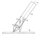
- Patent Document 1 discloses a pen-type input device that determines coordinates on a display image by detecting the amount and direction of movement of a pen tip. Specifically, as shown in FIG. 10, the light source 104 irradiates the writing surface 101 with laser light, and the speckle pattern generated by the reflection of the photodiode 105 on the writing surface 101 is detected to calculate the movement amount. The movement speed of the pen tip is obtained from the time correlation width of the speckle pattern detected by the means, and the movement amount is calculated by integrating the obtained movement speed, and the stress sensor 103 detects the stress in two directions orthogonal to the pen shaft 118. A pen-type input device 2 that detects the movement direction of the pen tip on the writing surface 101 from the magnitude of the stress in the two directions detected by the movement direction detection means is shown.
- Japanese Patent Publication Japanese Patent Laid-Open No. 9-114588 (published May 2, 1997)”
- Patent Document 1 has a problem in that it cannot be operated with high accuracy because the pointer on the display image is delayed when the pen is moved. Yes.
- the present invention has been made in view of the above-described conventional problems, and an object thereof is to provide a display device including an input unit that can be operated with high accuracy, a control method thereof, a control program for operating the display device, and a control program for operating the display device. It is to provide a recording medium.
- the present inventor has intensively studied the reason why the pointer on the display image is displayed with a delay when the pen is moved in the pen-type input device disclosed in Patent Document 1.
- the pen-type input device disclosed in Patent Document 1 since the coordinate determination process is performed sequentially, when the pointer is displayed on the display image, the pen has already been moved from the position corresponding to the pointer. I found it moving.
- the present inventor finds the relationship between the shape of the light receiving area formed by the light from the light irradiation unit and the amount of movement of the pointer on the display image, and determines the position of the pointer based on the shape of the light receiving area. It is possible to correct this, and as a result, when the light irradiation unit is moved, the pointer on the display image is not displayed with a delay, and the present invention has been completed.
- the display device with an input unit of the present invention includes a display unit that displays a main image and an input unit that inputs position information of a pointer to be displayed on the display unit in order to solve the above-described problem.
- a display device with an input unit wherein the input unit includes a light detection unit that detects irradiation light from the light irradiation unit, and the correction unit is a position of an optical axis of irradiation light from the light irradiation unit.
- the position information of the pointer is input to the optical position detection unit as the position of the optical axis, and the correction unit receives the irradiation light from the light irradiation unit.
- a light shape detection unit that detects the shape of the light receiving area
- the display device further includes pointer position correction means for correcting the position of the pointer
- the pointer position correction means includes The shape of the light receiving area detected by the light shape detector When changes are characterized by correcting the position information of the pointer.
- the light position can be detected by the light position detection unit, it is possible to determine the position of the pointer before correction in the main image. Furthermore, when the light irradiation unit is moved, the light position can be continuously detected by the light position detection unit, so the correction direction (movement direction) from the position of the pointer before correction in the main image. ) Can be determined. In addition, since the shape of the light receiving region can be detected by the light shape detection unit, the correction amount (movement amount) from the position of the pointer before correction in the main image can be determined.
- the position of the corrected pointer in the main image can be determined.
- the display device with an input unit of the present invention can be operated with high accuracy.
- the control method for a display device with an input unit includes an input step including a display step of displaying a main image on the display unit, and an input step of inputting position information of a pointer to be displayed on the display unit.
- the input step includes a light detection step for detecting the irradiation light irradiated in the light irradiation step
- the correction step includes the irradiation light irradiated in the light irradiation step.
- An optical position detecting step for detecting the position of the optical axis, the position information of the pointer is input to the optical position detecting step as the optical axis position, and the correction step is irradiated by the light irradiation step; And a light shape detecting step for detecting the shape of the light receiving region that receives the irradiated light, and the display device control method corrects the position of the pointer.
- An inter-position correction step is further included, wherein the pointer position correction step corrects the position information of the pointer when the shape of the light receiving area detected by the light shape detection step changes. Yes.
- the light position can be detected by the light position detection step, so that the position of the pointer before correction in the main image can be determined. Further, when the light is moved in the light irradiation step, the light position can be continuously detected by the light position detection step, so that the correction direction (from the pointer position before correction in the main image) ( Moving direction) can be determined. Further, since the shape of the light receiving region can be detected by the light shape detection step, the correction amount (movement amount) from the position of the pointer before correction in the main image can be determined.
- the pointer position correcting step since the pointer position correcting step is provided, it is possible to determine the position of the corrected pointer in the main image.
- the control method of the display device with an input unit of the present invention can be controlled with high accuracy.
- the display device with an input unit includes a display unit that includes a display unit that displays a main image and an input unit that inputs position information of a pointer to be displayed on the display unit.
- the input unit includes a light detection unit that detects irradiation light from the light irradiation unit, and the correction unit detects an optical position of the optical axis of the irradiation light from the light irradiation unit.
- the position information of the pointer is input to the optical position detection unit as the position of the optical axis, and the correction unit is configured to receive a light receiving region that receives the irradiation light from the light irradiation unit.
- the display device further includes a pointer position correcting unit that corrects the position of the pointer, and the pointer position correcting unit is detected by the optical shape detecting unit.
- the position When the shape of the light receiving area changes, the position And it corrects the positional information of the printer.
- the display device with an input unit of the present invention has an effect that it can be operated with high accuracy.
- the control method for a display device with an input unit includes an input step including a display step of displaying a main image on the display unit, and an input step of inputting position information of a pointer to be displayed on the display unit.
- the input step includes a light detection step for detecting the irradiation light irradiated in the light irradiation step
- the correction step includes the irradiation light irradiated in the light irradiation step.
- An optical position detecting step for detecting the position of the optical axis, the position information of the pointer is input to the optical position detecting step as the optical axis position, and the correction step is irradiated by the light irradiation step; And a light shape detecting step for detecting the shape of the light receiving region that receives the irradiated light, and the display device control method corrects the position of the pointer. And further comprise inter position correcting step, the pointer position correction step is detected by the optical shape detection step, when the shape of the light receiving region is changed, a method of correcting the position information of the pointer.
- control method of the display device with an input unit according to the present invention has an effect that it can be controlled with high accuracy.
- a display device with an input unit (for example, a display device with a pen-type input unit, an optical pen system, etc.) inputs a display unit that displays a main image and position information of a pointer to be displayed on the display unit.
- a display unit with an input unit wherein the input unit includes a light detection unit that detects irradiation light from the light irradiation unit, and the correction unit is irradiated light from the light irradiation unit.
- the position information of the pointer is input to the optical position detection unit as the position of the optical axis, and the correction unit receives from the light irradiation unit.
- a light shape detection unit that detects the shape of the light receiving region that receives the irradiation light, and the display device further includes pointer position correction means for correcting the position of the pointer,
- the correction means is detected by the light shape detection unit. When the shape of the light region is changed, and corrects the positional information of the pointer.
- the light irradiation unit used in the present invention is not particularly limited as long as it has a function of irradiating light, and examples thereof include a light pen.
- the light used in the present invention is not particularly limited, and examples thereof include laser light, visible light, ultraviolet light, and infrared light.
- the input unit used in the present invention is not particularly limited as long as it has a function of detecting (accepting) light, and examples thereof include a plate member (pad) such as a sensor liquid crystal.
- a plate member such as a sensor liquid crystal.
- an image acquired by the input unit is a sub-image.
- the display unit used in the present invention is not particularly limited as long as it has a function of displaying a pointer and a function of displaying an image, and examples thereof include a display panel such as a liquid crystal panel.
- a display panel such as a liquid crystal panel.
- an image displayed on the display unit is a main image.
- the pointer used in the present invention is displayed on a display unit such as a liquid crystal panel based on output information from an input unit such as a sensor liquid crystal.
- Examples of the pointer used in the present invention include a cursor indicating a location pointed by a pointing device in a graphical user interface.
- the display device 50 with an input unit includes an information processing device (not shown).
- the information processing device include an MPU (micro processor unit), a CPU (central processing unit), and the like.
- the information processing device may be provided separately (externally) from the display panel (display unit) and the input unit, or may be provided inside the display panel. Or may be provided inside the input unit.
- information processing apparatus When the information processing apparatus is provided separately from the display panel and the input unit, information output from the input unit is input to the information processing apparatus, and processing (described as MPU 38) described later is performed in the information processing apparatus. After that, information processed by the information processing apparatus is input to the display panel, and an image is displayed on the display panel based on the information processed by the information processing apparatus.
- the information processing apparatus when the information processing apparatus is provided in the display panel, information output from the input unit is input to the display panel, and processing described later is performed in the information processing apparatus provided in the display panel. (Processing as MPU 38) is performed, and then an image is displayed based on information after processing by the information processing apparatus.
- the information processing apparatus when the information processing apparatus is provided in the input unit, the information processing apparatus provided in the input unit performs the processing described later (processing as the MPU 38), and then from the input unit.
- the output information is input to the display panel, and an image is displayed on the display panel based on the information processed by the information processing apparatus.
- “information” in “a display panel (display unit) that displays a pointer based on output information from the input unit” means that “information output from the input unit is processed by the information processing apparatus”. Information after being performed ”and“ information output from the input unit ”.
- the pointer position correction unit may be provided separately (as an external device) from the information processing device, the display panel (display unit), and the input unit. It may be provided inside the information processing apparatus, may be provided inside the display panel, or may be provided inside the input unit.
- the pointer position correction means increases the correction value at the position of the pointer when the area of the light receiving region is reduced.
- correction vector Movement vector ⁇ Still image area / Actual image area (1) Is preferably defined by:
- the magnitude of the correction vector represents a correction value (correction amount), and the magnitude of the movement vector represents a movement amount.
- the direction of the correction vector represents the correction direction at the position of the pointer, and the direction of the movement vector represents the movement direction of the pointer.
- the area of the light receiving region is assumed to change from the still image area to the actual image area.
- FIG. 1 is a functional block diagram of a display device 50 with an input unit according to the present invention.
- 1 mainly includes a panel driving circuit 31, a sensor built-in liquid crystal panel 32, a backlight 33, a backlight power supply circuit 34, a display processing unit 35, an A / D converter 36, and an illuminance sensor 27.
- the panel drive circuit 31, the sensor built-in liquid crystal panel 32, the backlight 33, the backlight power supply circuit 34, the A / D converter 36, and the illuminance sensor 27 are provided on a display panel (display unit) in the display device 50 with an input unit. Is provided.
- the input unit is provided in the sensor liquid crystal.
- the display processing unit 35 and the MPU 38 may be provided separately (externally) from the display panel and the input unit, may be built in the display panel, or may be built in the input unit. Also good.
- the correction unit 39 may be provided separately (externally) from the MPU 38, the display panel, and the input unit, may be built in the MPU 38, or may be built in the display panel. However, it may be built in the input unit. In the following description, an example in which the correction unit is provided separately from the MPU 38 will be described.
- the sensor built-in liquid crystal panel 32 (hereinafter also referred to as “liquid crystal panel 32”) includes a plurality of pixel circuits and a plurality of photosensors arranged two-dimensionally. Details of the liquid crystal panel 32 will be described later.
- the display data Din output from the display processing unit 35 is input to the display panel.
- the input display data Din is supplied to the panel drive circuit 31.
- the panel drive circuit 31 writes a voltage corresponding to the display data Din to the pixel circuit of the liquid crystal panel 32. As a result, an image based on the display data Din is displayed on the liquid crystal panel 32 by each pixel.
- the backlight 33 includes a plurality of LEDs (Light Emitting Diodes), and irradiates light (backlight light) to the back surface (the surface opposite to the user side) of the liquid crystal panel 32.
- the backlight power supply circuit 34 switches whether to supply the power supply voltage to the backlight 33 according to the backlight control signal BC output from the MPU 38 according to the ambient environment light level LX output from the illuminance sensor 27.
- the backlight power supply circuit 34 supplies a power supply voltage when the backlight control signal BC is at a high level and does not supply a power supply voltage when the backlight control signal BC is at a low level.
- the backlight 33 is turned on while the backlight control signal BC is at a high level, and is turned off while the backlight control signal BC is at a low level.
- the liquid crystal panel 32 outputs the output signal of the optical sensor as the sensor output signal SS.
- the A / D converter 36 converts the analog sensor output signal SS into a digital signal. Thereafter, if necessary, the D / S converter 37 converts this digital signal into a scanned image.
- the MPU 38 and the pointer position correction unit are detected by a sensor position detection unit (light position detection unit) 28 and a sensor shape detection unit (light shape detection unit) 29 in the correction unit 39 based on the sensor output signal SS (digital signal).
- the sensor (light) position and the sensor (light) shape are specified from the information output by the information output unit (not shown), and the pointer coordinates (position), correction amount (movement amount), and correction direction (movement) Direction). Specifically, the coordinates (position) of the pointer, the correction amount (movement amount), and the correction direction (movement direction) are calculated from the sensor output signal SS (digital signal) from the liquid crystal panel 32 and / or the scanned image. Then, the MPU 38 outputs data such as coordinates.
- the MPU 38 performs event determination processing based on the output data such as coordinates. Specifically, based on data such as coordinates output after the coordinate determination process, how the pen (light irradiation unit) that is irradiating light moves, for example, a gesture for drawing a straight line, a circle It is determined whether the gesture processing is a drawing gesture or the like. Thereafter, the MPU 38 executes an application based on the event determination. Specifically, a program for performing input and output and calculation is executed based on event determination.
- the display processing unit (information output unit) 35 performs display processing based on the information output by the executed program. Thereafter, the display processing unit 35 outputs the display data Din to the panel drive circuit 31 in the display panel based on the display-processed information.
- a control method for a display device with an input unit includes a display step for displaying a main image on a display unit, and an input step for inputting position information of a pointer to be displayed on the display unit.
- the input step includes a light detection step for detecting the irradiation light irradiated in the light irradiation step
- the correction step includes an optical axis of the irradiation light irradiated in the light irradiation step.
- the position information of the pointer is input to the optical position detection step as the position of the optical axis, and the correction step is irradiated by the light irradiation step.
- a light shape detecting step for detecting a shape of a light receiving region that receives irradiation light includes: a pointer that corrects the position of the pointer And further include location correction step, the pointer position correction step is detected by the optical shape detection step, when the shape of the light receiving region is changed, a method of correcting the position information of the pointer.
- the correction value at the position of the pointer is increased when the area of the light receiving region is reduced in the pointer position correction step.
- the correction value for the rate of change of the area of the light receiving region is defined by the equation (1) in the pointer position correction step.
- control method of the display device with an input unit according to the present invention is controlled according to the functional block diagram of the display device with an input unit 50 according to the present invention shown in FIG.
- the display step is controlled by the display unit
- the input step is controlled by the input unit
- the light irradiation step is controlled by the light irradiation unit
- the light position detection step is a sensor position detection unit (light position detection unit). 28
- the light shape detection step is controlled by the sensor shape detection unit (light shape detection unit 29)
- the pointer position correction step is controlled by the pointer position correction unit (pointer position correction means).
- a correction value (correction amount, movement amount) at the position of the pointer in the display unit is derived from the shape of the light receiving area, and the position of the pointer is determined based on the position of the previously detected light. And the vector direction connecting the detected light position.
- the shape of the light receiving area of (A), (B) and (C) is smaller than the shape of the light receiving area of (0), so that the position of the pointer is corrected.
- the amount of movement is increased, that is, the acceleration is increased.
- the shape of the light receiving region (B) is larger than the shape of the light receiving region (A)
- the amount of movement between (A) and (B) is reduced, that is, the acceleration is reduced.
- the light is moving. Since the shape of the light receiving region in (C) is smaller than the shape of the light receiving region in (B), light is increased between (B) and (C) while increasing the amount of movement, that is, increasing the acceleration. It is moved.
- the sensor illuminance of the light decreases as the movement amount of the pen (light irradiation unit) increases, that is, as the acceleration increases.
- the sensor image (sensor position and sensor shape, light position and light receiving area shape) is acquired at a shutter speed of 60 Hz, 120 Hz, etc.
- the sensor shape (light receiving area of the light receiving area) is stopped as the pen (light irradiation unit) stops. Shape). Therefore, if the shape of the light receiving area is the largest when the light receiving area is stationary, the current position of the light receiving area is small and the position (coordinates) of the light is changing. I do.
- the shutter speed is not limited to 60 Hz or 120 Hz, and smoother as the speed is increased.
- the light receiving area detected at the present time when the shape of the light receiving area detected at the present time is smaller than that detected last time, the light is moved while increasing the movement amount, that is, increasing the acceleration.
- the shape of the light receiving region detected at the present time is larger than that detected last time, the light is moved while decreasing the movement amount, that is, decreasing the acceleration.
- the sensor image (sensor position and sensor shape, light position and light receiving area shape) is stored as a history and is referred to when calculating a vector.
- the input unit in the display device with an input unit of the present invention includes a light detection unit that detects irradiation light from the light irradiation unit. Furthermore, the correction unit has a light position detection unit and a light shape detection unit, the light position detection unit detects the position of the light emitted from the light irradiation unit, the light shape detection unit, The shape of the light receiving region formed by irradiating light from the light irradiation unit is detected.
- examples of the input unit in the present invention include an input unit (input device) such as a pen-type input unit, a digitizer, and a tablet.
- the input unit in the display device with an input unit of the present invention has a configuration and functions of a conventionally known input unit other than the configuration and functions described as the description of the functional block diagram described above.
- FIG. 4 is a circuit block diagram showing the circuit configuration of the liquid crystal panel 32 and the configuration of its peripheral circuits in the present invention.
- FIG. 5 shows an optical sensor in which the RGB color filters are arranged in stripes, and the photodiodes 39b are positioned in the same column as the blue picture elements 40b, that is, the photodiodes 39b are positioned on the back surface of the blue filter. This is an example when 30b is arranged.
- the color filter array may be an array other than the stripe array, such as a mosaic array or a delta array.
- the optical sensor 30r is arranged so that the photodiode 39r is positioned on the back surface of the same red filter as the red picture element 40r. And the optical sensor 30b of the blue picture element 40b and the optical sensor 30r of the red picture element 40r are regularly arranged in an approximately equal number.
- FIG. 5A is a schematic diagram illustrating an example of an arrangement state of the optical sensors 30 in this case.
- “R”, “G”, and “B” indicate a red picture element, a green picture element, and a blue picture element, respectively, and “S” indicates an optical sensor.
- the photosensor “S” is arranged in the blue picture element “B”, and in the pixels 4b and 4d, the photosensor “S” is arranged in the red picture element 4b.
- the picture element in which the optical sensor “S” is arranged is different for each horizontal line, but the arrangement rule is not limited to this.
- the optical sensor “S” may be arranged in different picture elements for each vertical line.
- the optical sensor “S” may be arranged in different picture elements for each adjacent pixel.
- the optical sensor “S” may be provided for each picture element.
- the optical sensor 30g is arranged so that the photodiode 39g is located on the back surface of the same green filter as the green picture element 40g. ing.
- the optical sensors 30b of the blue picture elements 40b and the optical sensors 30g of the green picture elements 40g are regularly arranged in an approximately equal number.
- the liquid crystal panel 32 includes m scanning signal lines G1 to Gm, 3n data signal lines SR1 to SRn, SG1 to SGn, SB1 to SBn, and (m ⁇ 3n) pixel circuits.
- the scanning signal lines G1 to Gm are arranged in parallel to each other.
- the data signal lines SR1 to SRn, SG1 to SGn, and SB1 to SBn are arranged in parallel to each other so as to be orthogonal to the scanning signal lines G1 to Gm.
- the sensor readout lines RW1 to RWm and the sensor reset lines RS1 to RSm are arranged in parallel with the scanning signal lines G1 to Gm.
- One pixel circuit 40 (40r, 40g, 40b) is provided in the vicinity of the intersection of the scanning signal lines G1 to Gm and the data signal lines SR1 to SRn, SG1 to SGn, and SB1 to SBn.
- the pixel circuits 40 are arranged two-dimensionally as a whole, m in the column direction (vertical direction in FIG. 4) and 3n in the row direction (horizontal direction in FIG. 4).
- the pixel circuit 40 is classified into a red (R) pixel circuit 40r, a green (G) pixel circuit 40g, and a blue (B) pixel circuit 40b according to the color of the color filter provided.
- RGB red
- G green
- B blue
- pixel circuits 40r, 40g, and 40b Three types of pixel circuits 40r, 40g, and 40b (hereinafter also referred to as “picture elements (sub-pixels)”) are arranged side by side in the row direction, and three pixels form one pixel.
- the pixel circuit 40 includes a thin film transistor (TFT) 32a and a liquid crystal capacitor 32b.
- the gate terminal of the TFT 32a is connected to the scanning signal line Gi (i is an integer of 1 to m), and the source terminal is one of the data signal lines SRj, SGj, SBj (j is an integer of 1 to n).
- the drain terminal is connected to one electrode of the liquid crystal capacitor 32b.
- a common electrode voltage is applied to the other electrode of the liquid crystal capacitor 32b.
- the data signal lines SG1 to SGn connected to the green (G) pixel circuit 40g are referred to as G data signal lines
- the data signal lines SB1 to SBn connected to the blue (B) pixel circuit 40b are referred to as B data signal lines.
- the pixel circuit 40 may include an auxiliary capacitor.
- the light transmittance (pixel brightness) of the pixel circuit 40 is determined by the voltage written in the pixel circuit 40.
- a high level voltage TFT 32a is turned on
- Voltage to be set may be applied, and a voltage to be written to the data signal line SXj may be applied.
- the optical sensor 30 includes a capacitor 39a, a photodiode 39b, and a sensor preamplifier 39c, and is provided at least for each blue picture element 40b (blue (B) pixel circuit 40b).
- the sensor preamplifier 39c includes a TFT having a gate terminal connected to the node A, a drain terminal connected to the B data signal line SBj, and a source terminal connected to the G data signal line SGj.
- a predetermined value is applied to the sensor readout line RWi and the sensor reset line RSi at the timing of the timing chart shown in FIG.
- a voltage may be applied and the power supply voltage VDD may be applied to the B data signal line SBj.
- the power supply voltage VDD When the power supply voltage VDD is applied to the B data signal line SBj, the voltage at the node A is amplified by the sensor preamplifier 39c, and the amplified voltage is output to the G data signal line SGj. Therefore, the amount of light detected by the optical sensor 30 can be obtained based on the voltage of the G data signal line SGj.
- a scanning signal line driving circuit 41 Around the liquid crystal panel 32, a scanning signal line driving circuit 41, a data signal line driving circuit 42, a sensor row driving circuit 43, p (p is an integer between 1 and n) sensor output amplifiers 44 and a plurality of switches 45. To 48 are provided.
- the scanning signal line drive circuit 41, the data signal line drive circuit 42, and the sensor row drive circuit 43 correspond to the panel drive circuit 31 in FIG.
- the data signal line driving circuit 42 has 3n output terminals corresponding to 3n data signal lines.
- One switch 45 is provided between each of the G data signal lines SG1 to SGn and n output terminals corresponding thereto, and the B data signal lines SB1 to SBn and n output terminals corresponding thereto are connected.
- One switch 46 is provided between them.
- the G data signal lines SG1 to SGn are divided into p groups, and the kth (k is an integer of 1 to p) G data signal lines and the input terminals of the kth sensor output amplifier 44 in the group.
- One switch 47 is provided between each switch.
- the B data signal lines SB1 to SBn are all connected to one end of the switch 48, and the power supply voltage VDD is applied to the other end of the switch 48.
- the number of switches 45 to 47 included in FIG. 4 is n, and the number of switches 48 is one.
- the circuit shown in FIG. 4 performs different operations in the display period and the sensing period.
- the switches 45 and 46 are turned on, and the switches 47 and 48 are turned off.
- the switches 45 and 46 are in the off state, the switch 48 is in the on state, and the switch 47 is configured so that the G data signal lines SG1 to SGn are connected to the input terminal of the sensor output amplifier 44 in order for each group. It is turned on in time division.
- the scanning signal line driving circuit 41 and the data signal line driving circuit 42 operate.
- the scanning signal line drive circuit 41 selects one scanning signal line from the scanning signal lines G1 to Gm every one line time according to the timing control signal C1, and applies a high level voltage to the selected scanning signal line. Then, a low level voltage is applied to the remaining scanning signal lines.
- the data signal line drive circuit 42 drives the data signal lines SR1 to SRn, SG1 to SGn, and SB1 to SBn in a line sequential manner based on the display data DR, DG, and DB.
- the data signal line drive circuit 42 stores the display data DR, DG, and DB for at least one row, and applies a voltage corresponding to the display data for one row for each line time to the data signal lines SR1 to SR1. Applied to SRn, SG1 to SGn, and SB1 to SBn. Note that the data signal line driving circuit 42 may drive the data signal lines SR1 to SRn, SG1 to SGn, and SB1 to SBn in a dot sequential manner.
- the sensor row driving circuit 43 and the sensor output amplifier 44 operate.
- the sensor row driving circuit 43 selects one signal line for each line time from the sensor readout lines RW1 to RWm and the sensor reset lines RS1 to RSm according to the timing control signal C2, and selects the selected sensor readout line and A predetermined readout voltage and reset voltage are applied to the sensor reset line, and voltages different from those at the time of selection are applied to the other signal lines.
- the length of one line time differs between the display period and the sensing period.
- the sensor output amplifier 44 amplifies the voltage selected by the switch 47 and outputs it as sensor output signals SS1 to SSp.
- the backlight control signal BC is at a high level during the display period and is at a low level during the sensing period.
- the backlight 33 is turned on during the display period and is turned off during the sensing period. For this reason, the influence of the backlight light on the photodiode 39b can be reduced.
- FIG. 7 is an example of a cross-sectional view showing the configuration of the liquid crystal panel 32 in the present invention.
- the liquid crystal panel 32 has, for example, a structure in which a liquid crystal layer 52 is sandwiched between two glass substrates 51a and 51b.
- One glass substrate 51a includes, for example, three color filters 53r, 53g, and 53b, a light shielding film 54, a counter electrode 55, and the like
- the other glass substrate 51b includes, for example, a pixel electrode 56 and data.
- a signal line 57, an optical sensor 30, and the like are provided.
- the optical sensor 30 is provided in the vicinity of the pixel electrode 56 provided with a blue color filter 53b, for example.
- at least the photodiode 39 b of the optical sensor 30 is preferably arranged on the back surface of the center of the color filter 53 in order to reliably receive the light transmitted through the color filter 53.
- An alignment film 58 is provided on the opposing surfaces of the glass substrates 51a and 51b, and a polarizing plate 59 is provided on the other surface.
- a polarizing plate 59 is provided on the other surface.
- the surface on the glass substrate 51a side is the surface
- the surface on the glass substrate 51b side is the back surface.
- the backlight 33 is provided on the back side of the liquid crystal panel 32.
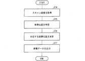
- FIG. 8 is a flowchart showing an example of processing for specifying a position irradiated with light in the display device with an input unit 50 according to the present invention.
- the processing shown in FIG. 8 is performed within one frame time by the MPU 38 shown in FIG.
- the A / D converter 36 (see FIG. 1) converts the analog output signal SS output from the optical sensor 30 built in the liquid crystal panel 32 into a digital signal.
- the MPU 38 acquires this digital signal as a scanned image (step S74). Further, the MPU 38 performs a process for specifying the pixel position on the acquired scan image (step S75).
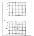
- FIG. 9A is a schematic diagram of a scanned image having the number of pixels of m ⁇ n.
- (a) of FIG. 9 when the scanned image is binarized based on a predetermined threshold, it is determined that a pixel having a value of “1” is a pixel irradiated with light, The pixel position in this pixel is specified.
- the pixel position (Xn-i, Ym-j) is specified.
- FIG. 9B shows a scan image when light is irradiated to a plurality of pixels.
- the pixel position specified in this case includes eight pixels around the pixel position (Xn-i, Ym-j). Note that the scan image of FIG. 9B is obtained in the case of the arrangement rule shown in FIG. 5D or FIG. 5E.
- the MPU 38 performs a process of determining coordinates (position) in the image corresponding to the specified pixel (step S76). For example, as shown in FIG. 9A, coordinates corresponding to the specified pixel position (Xn-i, Ym-j) are determined. When the image resolution of the display image and the screen resolution of the liquid crystal panel match at “m ⁇ n”, the pixel position (Xn ⁇ i, Ym ⁇ j) is determined as the coordinates (position). If the image resolution and the screen resolution do not match, coordinate conversion may be performed to determine the coordinates (position) corresponding to the pixel position.
- the coordinates (position) are determined based on a predetermined rule. do it.
- the coordinates (position) may be determined based on the pixel closest to the specified pixel's center of gravity.
- the corresponding coordinates can be determined based on the pixel position (Xn-i, Ym-j) corresponding to the center of gravity of the plurality of pixels having the value "1".
- coordinates corresponding to all pixel positions having a value “1” may be determined as coordinates (positions).
- the MPU 38 When the coordinates (position) are determined, the MPU 38 outputs the coordinate data at the determined coordinates to the panel drive circuit 31 in the display panel (step S77).
- the process of specifying the position and shape of the irradiated light is performed as follows. This process is performed by the MPU 38 shown in FIG.
- the A / D converter 36 (see FIG. 1) converts the analog output signal SS output from the optical sensor 30 built in the liquid crystal panel 32 into a digital signal. Then, the MPU 38 acquires this digital signal as a sensor image.
- the MPU 38 can perform processing for specifying the edge extraction image from the acquired sensor image.
- the MPU 38 When the edge extracted image is specified, the MPU 38 performs a process of determining a moving direction corresponding to the specified edge extracted image. When the moving direction is determined, the MPU 38 outputs data in the determined moving direction to the panel drive circuit 31 in the display panel.
- Each block (configuration) of the display device with an input unit of the present invention may be configured by hardware logic, or may be realized by software using a CPU as follows.
- the display device with an input unit of the present invention includes a CPU (central processing unit) that executes instructions of a control program that realizes each function, a ROM (read only memory) that stores the program, and a RAM ( random access memory), a storage device (recording medium) such as a memory for storing the program and various data.
- a CPU central processing unit
- ROM read only memory
- RAM random access memory
- storage device recording medium
- An object of the present invention is a recording in which a program code (execution format program, intermediate code program, source program) of a control program for the display device with an input unit, which is software for realizing the functions described above, is recorded so as to be read by a computer
- a program code execution format program, intermediate code program, source program
- This can also be achieved by supplying the medium to the display device with an input unit, and reading and executing the program code recorded on the recording medium by the computer (or CPU or MPU).
- Examples of the recording medium include tapes such as magnetic tapes and cassette tapes, magnetic disks such as floppy (registered trademark) disks / hard disks, and disks including optical disks such as CD-ROM / MO / MD / DVD / CD-R.
- Card system such as IC card, IC card (including memory card) / optical card, or semiconductor memory system such as mask ROM / EPROM / EEPROM / flash ROM.
- the display device with an input unit may be configured to be connectable to a communication network, and the program code may be supplied via the communication network.
- the communication network is not particularly limited.
- the Internet intranet, extranet, LAN, ISDN, VAN, CATV communication network, virtual private network, telephone line network, mobile communication network, satellite communication. A net or the like is available.
- the transmission medium constituting the communication network is not particularly limited.
- wired such as IEEE 1394, USB, power line carrier, cable TV line, telephone line, ADSL line, etc.
- infrared rays such as IrDA and remote control, Bluetooth (Registered trademark), 802.11 wireless, HDR, mobile phone network, satellite line, terrestrial digital network, and the like can also be used.
- the present invention can also be realized in the form of a computer data signal embedded in a carrier wave in which the program code is embodied by electronic transmission.
- the pointer position correction unit increases the correction value at the pointer position when the area of the light receiving region is reduced.
- the display device with an input unit of the present invention can easily determine the position of the corrected pointer, and can be operated with higher accuracy.
- correction vector Movement vector ⁇ Still image area / Actual image area (1) Is preferably defined by:
- the display device with an input unit of the present invention can easily determine the correction amount (movement amount) from the position of the pointer before correction, and thus can be operated more easily and accurately.
- the correction value at the position of the pointer is increased when the area of the light receiving region is reduced in the pointer position correction step.
- control method of the display device with an input unit according to the present invention can easily determine the position of the corrected pointer, and thus can be controlled with higher accuracy.
- Correction vector Movement vector ⁇ Still image area / Actual image area (1) Is preferably defined by:
- control method for the display device with an input unit can easily determine the correction amount (movement amount) from the position of the pointer before correction, and thus can be controlled more easily and accurately.
- the control program of the present invention is a control program for operating the display device with an input unit, and is for causing a computer to function as each unit described above.
- the recording medium of the present invention is a computer-readable medium on which the control program is recorded.
- the display device with an input unit of the present invention can be realized by a computer.
- the display device with an input unit of the present invention can be used for display devices such as a personal computer, an electronic dictionary, a car navigation device, a portable information terminal, a game machine, and an electronic blackboard.
- Illuminance sensor 28 Sensor position detector (light position detector) 29 Sensor shape detector (light shape detector) DESCRIPTION OF SYMBOLS 30 Photosensor 31 Panel drive circuit 32 Sensor built-in liquid crystal panel 33 Backlight 34 Backlight power supply circuit 35 Display processing part 36 A / D converter 37 D / S converter 38 Microprocessor unit (MPU) 39 correction unit 41 scanning signal line drive circuit 42 data signal line drive circuit 43 sensor row drive circuit 44 sensor output amplifier 45 switch 46 switch 47 switch 48 switch 50 display device with input unit
Landscapes
- Engineering & Computer Science (AREA)
- General Engineering & Computer Science (AREA)
- Theoretical Computer Science (AREA)
- Human Computer Interaction (AREA)
- Physics & Mathematics (AREA)
- General Physics & Mathematics (AREA)
- Position Input By Displaying (AREA)
Abstract
精度良く操作することができる入力部付き表示装置を提供する。本発明の入力部付き表示装置(50)は、補正部(39)が、光照射部からの照射光の光軸の位置を検知するセンサ位置検知部(28)を有しており、ポインタの位置情報は、光軸の位置としてセンサ位置検知部(28)に入力され、補正部(39)が、光照射部からの照射光を受容している受光領域の形状を検知するセンサ形状検知部(29)を有しており、入力部付き表示装置(50)は、ポインタの位置を補正するポインタ位置補正手段をさらに備えており、ポインタ位置補正手段は、センサ形状検知部(29)が検知する、受光領域の形状が変化したときに、ポインタの位置情報を補正する。
Description
本発明は、入力部付き表示装置およびその制御方法、並びに制御プログラムおよび記録媒体に関するものである。さらに詳しくは、精度良く操作することができる入力部付き表示装置およびその制御方法、並びにそれを動作させる制御プログラムおよび記録媒体に関するものである。
従来、表示装置への情報の入力部としては、キーボード、マウス、タッチパネル、デジタイザ、タブレット、ペン型入力部等が用いられている。その中で、ペン型入力部において、表示装置における表示画像の移動、コマンド選択等を行う際には、当該表示画像に対応する画像を表示する板状部材に対して光を照射するペンにて、当該板状部材に入力を行っている。
ペン型入力部として、例えば特許文献1には、ペン先の移動量および移動方向を検出することによって表示画像上の座標を決定するペン型入力装置が示されている。具体的には、図10に示すように、光源104が筆記面101に対してレーザ光を照射し、フォトダイオード105が筆記面101で反射して発生したスペックルパターンを検出し、移動量算出手段が検出したスペックルパターンの時間相関幅からペン先の移動速度を求め、求めた移動速度を積分して移動量を計算し、応力センサ103がペン軸118と直交する2方向の応力を検出し、移動方向検出手段が検出した2方向の応力の大きさからペン先の筆記面101上における移動方向を検出するペン型入力装置2が示されている。
しかしながら、上記特許文献1に示されているペン型入力装置では、ペンを移動させる際に表示画像上のポインタが遅れて表示されるため、精度良く操作することができないという問題点を有している。
本発明は、上記従来の問題点に鑑みてなされたものであって、その目的は、精度良く操作することができる入力部を備えた表示装置およびその制御方法、並びにそれを動作させる制御プログラムおよび記録媒体を提供することにある。
本発明者は、上記課題に鑑み、上記特許文献1に示されているペン型入力装置において、ペンを移動させる際に表示画像上のポインタが遅れて表示される理由を、鋭意検討した。その結果、上記特許文献1に示されているペン型入力装置では、座標決定処理をシーケンシャルに行うため、表示画像上にポインタが表示される時点において、当該ペンが当該ポインタに対応する位置からすでに移動していることを見出した。
そして、本発明者は、光照射部からの光によって形成される受光領域の形状と、表示画像上のポインタの移動量との関係を見出し、当該受光領域の形状に基づいて当該ポインタの位置を補正することが可能であり、これによって、光照射部を移動させる際に表示画像上のポインタが遅れて表示されないことを独自に見出し、本発明を完成させるに至った。
すなわち、本発明の入力部付き表示装置は、上記の課題を解決するために、主画像を表示する表示部と、該表示部上に表示されるべきポインタの位置情報を入力する入力部とを備えた入力部付き表示装置であって、上記入力部は、光照射部からの照射光を検知する光検知部を有し、補正部は、上記光照射部からの照射光の光軸の位置を検知する光位置検知部を有しており、上記ポインタの位置情報は、該光軸の位置として該光位置検知部に入力され、上記補正部は、上記光照射部からの照射光を受容している受光領域の形状を検知する光形状検知部を有しており、上記表示装置は、上記ポインタの位置を補正するポインタ位置補正手段をさらに備えており、上記ポインタ位置補正手段は、上記光形状検知部が検知する、上記受光領域の形状が変化したときに、上記ポインタの位置情報を補正することを特徴としている。
上記の構成によれば、上記光位置検知部により光の位置を検知することができるので、上記主画像における補正前のポインタの位置を決定することができる。さらに、上記光照射部を移動させる場合には、上記光位置検知部により光の位置を連続的に検知することができるので、上記主画像における補正前のポインタの位置からの補正方向(移動方向)を決定することができる。また、上記光形状検知部により受光領域の形状を検知することができるので、上記主画像における補正前のポインタの位置からの補正量(移動量)を決定することができる。
また、上記の構成によれば、ポインタ位置補正手段を備えているので、上記主画像における補正後のポインタの位置を決定することができる。
これにより、光照射部を移動させる際に、主画像上のポインタを、当該光照射部から照射される光の位置に対して遅れないように表示することができる。その結果、本発明の入力部付き表示装置は、精度良く操作することができる。
また、本発明の入力部付き表示装置の制御方法は、表示部上に主画像を表示する表示ステップと、該表示部上に表示されるべきポインタの位置情報を入力する入力ステップとを含む入力部付き表示装置の制御方法であって、上記入力ステップは、光照射ステップによって照射される照射光を検知する光検知ステップを有し、補正ステップは、上記光照射ステップによって照射される照射光の光軸の位置を検知する光位置検知ステップを有しており、上記ポインタの位置情報は、該光軸の位置として該光位置検知ステップに入力され、上記補正ステップは、上記光照射ステップによって照射される照射光を受容している受光領域の形状を検知する光形状検知ステップを有しており、上記表示装置の制御方法は、上記ポインタの位置を補正するポインタ位置補正ステップをさらに含んでおり、上記ポインタ位置補正ステップは、上記光形状検知ステップによって検知される、上記受光領域の形状が変化したときに、上記ポインタの位置情報を補正することを特徴としている。
上記の構成によれば、上記光位置検知ステップにより光の位置を検知することができるので、上記主画像における補正前のポインタの位置を決定することができる。さらに、上記光照射ステップにおいて光を移動させる場合には、上記光位置検知ステップにより光の位置を連続的に検知することができるので、上記主画像における補正前のポインタの位置からの補正方向(移動方向)を決定することができる。また、上記光形状検知ステップにより受光領域の形状を検知することができるので、上記主画像における補正前のポインタの位置からの補正量(移動量)を決定することができる。
また、上記の構成によれば、ポインタ位置補正ステップを備えているので、上記主画像における補正後のポインタの位置を決定することができる。
これにより、光照射ステップにおいて光を移動させる際に、主画像上のポインタを、当該光の位置に対して遅れないように表示することができる。その結果、本発明の入力部付き表示装置の制御方法は、精度良く制御することができる。
本発明の入力部付き表示装置は、以上のように、主画像を表示する表示部と、該表示部上に表示されるべきポインタの位置情報を入力する入力部とを備えた入力部付き表示装置であって、上記入力部は、光照射部からの照射光を検知する光検知部を有し、補正部は、上記光照射部からの照射光の光軸の位置を検知する光位置検知部を有しており、上記ポインタの位置情報は、該光軸の位置として該光位置検知部に入力され、上記補正部は、上記光照射部からの照射光を受容している受光領域の形状を検知する光形状検知部を有しており、上記表示装置は、上記ポインタの位置を補正するポインタ位置補正手段をさらに備えており、上記ポインタ位置補正手段は、上記光形状検知部が検知する、上記受光領域の形状が変化したときに、上記ポインタの位置情報を補正するものである。
それゆえ、本発明の入力部付き表示装置は、精度良く操作することができるという効果を奏する。
また、本発明の入力部付き表示装置の制御方法は、表示部上に主画像を表示する表示ステップと、該表示部上に表示されるべきポインタの位置情報を入力する入力ステップとを含む入力部付き表示装置の制御方法であって、上記入力ステップは、光照射ステップによって照射される照射光を検知する光検知ステップを有し、補正ステップは、上記光照射ステップによって照射される照射光の光軸の位置を検知する光位置検知ステップを有しており、上記ポインタの位置情報は、該光軸の位置として該光位置検知ステップに入力され、上記補正ステップは、上記光照射ステップによって照射される照射光を受容している受光領域の形状を検知する光形状検知ステップを有しており、上記表示装置の制御方法は、上記ポインタの位置を補正するポインタ位置補正ステップをさらに含んでおり、上記ポインタ位置補正ステップは、上記光形状検知ステップによって検知される、上記受光領域の形状が変化したときに、上記ポインタの位置情報を補正する方法である。
それゆえ、本発明の入力部付き表示装置の制御方法は、精度良く制御することができるという効果を奏する。
本発明の一実施形態について、以下に詳しく説明するが、本発明の範囲はこれらの説明に拘束されることはなく、以下の例示以外についても、本発明の趣旨を損なわない範囲で適宜変更して実施し得るものである。具体的には、本発明は以下の実施形態に限定されるものではなく、請求項に示した範囲で種々の変更が可能である。すなわち、請求項に示した範囲で適宜変更した技術的手段を組み合わせて得られる実施形態についても本発明の技術的範囲に含まれる。
<本発明の入力部付き表示装置の構成>
本発明の入力部付き表示装置(例えば、ペン型入力部付き表示装置、光ペンシステム等)は、主画像を表示する表示部と、該表示部上に表示されるべきポインタの位置情報を入力する入力部とを備えた入力部付き表示装置であって、上記入力部は、光照射部からの照射光を検知する光検知部を有し、補正部は、上記光照射部からの照射光の光軸の位置を検知する光位置検知部を有しており、上記ポインタの位置情報は、該光軸の位置として該光位置検知部に入力され、上記補正部は、上記光照射部からの照射光を受容している受光領域の形状を検知する光形状検知部を有しており、上記表示装置は、上記ポインタの位置を補正するポインタ位置補正手段をさらに備えており、上記ポインタ位置補正手段は、上記光形状検知部が検知する、上記受光領域の形状が変化したときに、上記ポインタの位置情報を補正するものである。
本発明の入力部付き表示装置(例えば、ペン型入力部付き表示装置、光ペンシステム等)は、主画像を表示する表示部と、該表示部上に表示されるべきポインタの位置情報を入力する入力部とを備えた入力部付き表示装置であって、上記入力部は、光照射部からの照射光を検知する光検知部を有し、補正部は、上記光照射部からの照射光の光軸の位置を検知する光位置検知部を有しており、上記ポインタの位置情報は、該光軸の位置として該光位置検知部に入力され、上記補正部は、上記光照射部からの照射光を受容している受光領域の形状を検知する光形状検知部を有しており、上記表示装置は、上記ポインタの位置を補正するポインタ位置補正手段をさらに備えており、上記ポインタ位置補正手段は、上記光形状検知部が検知する、上記受光領域の形状が変化したときに、上記ポインタの位置情報を補正するものである。
ここで、本発明に用いられる光照射部は、光を照射する機能を有していれば特に限定されず、例えば、光ペン等が挙げられる。
本発明に用いられる光は、特に限定されず、例えば、レーザ光、可視光、紫外光、赤外光等が挙げられる。
本発明に用いられる入力部は、光を検知(受容)する機能を有していれば特に限定されず、例えば、センサ液晶等の板状部材(パッド)などが挙げられる。本明細書において、入力部で取得される画像を副画像とする。
本発明に用いられる表示部は、ポインタを表示する機能および画像を表示する機能を有していれば特に限定されず、例えば、液晶パネル等の表示パネルなどが挙げられる。本明細書において、表示部に表示される画像を主画像とする。
本発明に用いられるポインタは、センサ液晶等の入力部からの出力情報に基づいて液晶パネル等の表示部に表示されるものである。本発明に用いられるポインタとしては、例えば、グラフィカルユーザインタフェースにおいてポインティングデバイスが指し示している場所を表すカーソル等が挙げられる。
ここで、本発明における入力部付き表示装置50は、情報処理装置(図示しない)を備えている。情報処理装置としては、例えば、MPU(micro processor unit)、CPU(central processing unit、中央(演算)処理装置)等が挙げられる。
本発明における入力部付き表示装置50において、上記情報処理装置は、表示パネル(表示部)および入力部とは別個に(外付けとして)備えられていてもよいし、表示パネルの内部に備えられていてもよいし、入力部の内部に備えられていてもよい。
上記情報処理装置が表示パネルおよび入力部とは別個に備えられている場合には、入力部から出力された情報が上記情報処理装置に入力され、上記情報処理装置において後述の処理(MPU38としての処理)を行い、その後、上記情報処理装置による処理後の情報が表示パネルに入力され、表示パネルにおいて上記情報処理装置による処理後の情報に基づいて画像を表示する。
一方、上記情報処理装置が表示パネルの内部に備えられている場合には、入力部から出力された情報が表示パネルに入力され、表示パネルの内部に備えられた上記情報処理装置において後述の処理(MPU38としての処理)を行い、その後、上記情報処理装置による処理後の情報に基づいて画像を表示する。
また、上記情報処理装置が入力部の内部に備えられている場合には、入力部の内部に備えられた上記情報処理装置において後述の処理(MPU38としての処理)を行い、その後、入力部から出力された情報が表示パネルに入力され、表示パネルにおいて上記情報処理装置による処理後の情報に基づいて画像を表示する。
すなわち、本発明において、「入力部からの出力情報に基づいてポインタを表示する表示パネル(表示部)」における「情報」とは、「入力部から出力された情報を、上記情報処理装置により処理した後の情報」と、「入力部から出力された情報」とを含む。
本発明における入力部付き表示装置50において、上記ポインタ位置補正手段は、上記情報処理装置、表示パネル(表示部)および入力部とは別個に(外付けとして)備えられていてもよいし、上記情報処理装置の内部に備えられていてもよいし、表示パネルの内部に備えられていてもよいし、入力部の内部に備えられていてもよい。
また、本発明の入力部付き表示装置は、上記ポインタ位置補正手段において、上記受光領域の面積が小さくなったときに、上記ポインタの位置における補正値を大きくすることが好ましい。
また、本発明の入力部付き表示装置は、上記ポインタ位置補正手段において、上記受光領域の面積の変化率に対する上記補正値が、次に示す式(1)
補正ベクトル = 移動ベクトル × 静止画像面積 / 実画像面積・・・(1)
によって規定されることが好ましい。
補正ベクトル = 移動ベクトル × 静止画像面積 / 実画像面積・・・(1)
によって規定されることが好ましい。
式(1)において、補正ベクトルの大きさが補正値(補正量)を表し、移動ベクトルの大きさが移動量を表す。また、補正ベクトルの向きが上記ポインタの位置における補正方向を表し、移動ベクトルの向きが上記ポインタの移動方向を表す。また、式(1)において、受光領域の面積は、静止画像面積から実画像面積に変化するものとしている。
<本発明の入力部付き表示装置の機能ブロック図>
図1は、本発明における入力部付き表示装置50の機能ブロック図である。図1に示す入力部付き表示装置50は、主として、パネル駆動回路31、センサ内蔵液晶パネル32、バックライト33、バックライト電源回路34、表示処理部35、A/D変換器36、照度センサ27、マイクロプロセッサユニット(以下、MPUとする。)38および補正部39を備えている。
図1は、本発明における入力部付き表示装置50の機能ブロック図である。図1に示す入力部付き表示装置50は、主として、パネル駆動回路31、センサ内蔵液晶パネル32、バックライト33、バックライト電源回路34、表示処理部35、A/D変換器36、照度センサ27、マイクロプロセッサユニット(以下、MPUとする。)38および補正部39を備えている。
ここで、パネル駆動回路31、センサ内蔵液晶パネル32、バックライト33、バックライト電源回路34、A/D変換器36および照度センサ27は、入力部付き表示装置50における表示パネル(表示部)に備えられている。また、入力部は、センサ液晶に備えられている。一方、表示処理部35およびMPU38は、表示パネルおよび入力部とは別個に(外付けとして)備えられていてもよいし、表示パネルに内蔵されていてもよいし、入力部に内蔵されていてもよい。また、補正部39は、MPU38、表示パネルおよび入力部とは別個に(外付けとして)備えられていてもよいし、MPU38に内蔵されていてもよいし、表示パネルに内蔵されていてもよいし、入力部に内蔵されていてもよい。なお、以下の説明では、補正部がMPU38と別に備えられている例を挙げて説明する。
センサ内蔵液晶パネル32(以下、「液晶パネル32」ともいう。)は、2次元状に配置された複数の画素回路と複数の光センサとを含んでいる。なお、液晶パネル32の詳細については後述する。
表示パネルには、表示処理部35より出力される表示データDinが入力される。入力された表示データDinは、パネル駆動回路31に供給される。パネル駆動回路31は、液晶パネル32の画素回路に表示データDinに応じた電圧を書き込む。これにより、液晶パネル32には表示データDinに基づく画像が各画素によって表示される。
バックライト33は、複数のLED(Light Emitting Diode)を含み、液晶パネル32の背面(ユーザ側と反対の面)に光(バックライト光)を照射する。バックライト電源回路34は、照度センサ27から出力された周辺環境光レベルLXにより、MPU38から出力されたバックライト制御信号BCに従い、バックライト33に電源電圧を供給するか否かを切り替える。以下、バックライト電源回路34は、バックライト制御信号BCがハイレベルのときには電源電圧を供給し、バックライト制御信号BCがローレベルのときには電源電圧を供給しないものとする。バックライト33は、バックライト制御信号BCがハイレベルである間は点灯し、バックライト制御信号BCがローレベルである間は消灯する。
液晶パネル32は、光センサの出力信号をセンサ出力信号SSとして出力する。A/D変換器36は、アナログのセンサ出力信号SSをデジタル信号に変換する。その後、必要に応じて、D/S変換器37がこのデジタル信号をスキャン画像に変換する。
MPU38およびポインタ位置補正部は、センサ出力信号SS(デジタル信号)に基づいて、補正部39におけるセンサ位置検知部(光位置検知部)28およびセンサ形状検知部(光形状検知部)29によって検知され、かつ情報出力部(図示しない)によって出力された情報からセンサ(光)位置およびセンサ(光)形状の特定処理を行い、ポインタの座標(位置)並びに補正量(移動量)および補正方向(移動方向)を決定する。具体的には、液晶パネル32からのセンサ出力信号SS(デジタル信号)および/またはスキャン画像により、ポインタの座標(位置)並びに補正量(移動量)および補正方向(移動方向)を算出する。そして、MPU38は、座標等のデータを出力する。その後、MPU38は、出力された座標等のデータに基づいて、イベント判断処理を行う。具体的には、座標決定処理後に出力された座標等のデータに基づいて、光を照射しているペン(光照射部)がどのように移動しているか、例えば、直線を描くジェスチャー、円を描くジェスチャー等のジェスチャー処理であるかなどを判断する。その後、MPU38は、イベント判断に基づいて、アプリケーションを行う。具体的には、イベント判断に基づいて、入力および出力、並びに演算を行うプログラムを実行する。
その後、表示処理部(情報出力部)35は、実行されたプログラムにより出力された情報に基づいて、表示処理を行う。その後、表示処理部35は、表示処理された情報に基づいて、表示パネル中のパネル駆動回路31に、表示データDinを出力する。
<本発明の入力部付き表示装置の制御方法>
本発明の入力部付き表示装置の制御方法は、表示部上に主画像を表示する表示ステップと、該表示部上に表示されるべきポインタの位置情報を入力する入力ステップとを含む入力部付き表示装置の制御方法であって、上記入力ステップは、光照射ステップによって照射される照射光を検知する光検知ステップを有し、補正ステップは、上記光照射ステップによって照射される照射光の光軸の位置を検知する光位置検知ステップを有しており、上記ポインタの位置情報は、該光軸の位置として該光位置検知ステップに入力され、上記補正ステップは、上記光照射ステップによって照射される照射光を受容している受光領域の形状を検知する光形状検知ステップを有しており、上記表示装置の制御方法は、上記ポインタの位置を補正するポインタ位置補正ステップをさらに含んでおり、上記ポインタ位置補正ステップは、上記光形状検知ステップによって検知される、上記受光領域の形状が変化したときに、上記ポインタの位置情報を補正する方法である。
本発明の入力部付き表示装置の制御方法は、表示部上に主画像を表示する表示ステップと、該表示部上に表示されるべきポインタの位置情報を入力する入力ステップとを含む入力部付き表示装置の制御方法であって、上記入力ステップは、光照射ステップによって照射される照射光を検知する光検知ステップを有し、補正ステップは、上記光照射ステップによって照射される照射光の光軸の位置を検知する光位置検知ステップを有しており、上記ポインタの位置情報は、該光軸の位置として該光位置検知ステップに入力され、上記補正ステップは、上記光照射ステップによって照射される照射光を受容している受光領域の形状を検知する光形状検知ステップを有しており、上記表示装置の制御方法は、上記ポインタの位置を補正するポインタ位置補正ステップをさらに含んでおり、上記ポインタ位置補正ステップは、上記光形状検知ステップによって検知される、上記受光領域の形状が変化したときに、上記ポインタの位置情報を補正する方法である。
また、本発明の入力部付き表示装置の制御方法は、上記ポインタ位置補正ステップにおいて、上記受光領域の面積が小さくなったときに、上記ポインタの位置における補正値を大きくすることが好ましい。
また、本発明の入力部付き表示装置の制御方法は、上記ポインタ位置補正ステップにおいて、上記受光領域の面積の変化率に対する上記補正値が、上記式(1)によって規定されることが好ましい。
具体的には、本発明の入力部付き表示装置の制御方法は、図1に示す本発明における入力部付き表示装置50の機能ブロック図にしたがって制御される。
ここで、表示ステップは、表示部によって制御され、入力ステップは、入力部によって制御され、光照射ステップは、光照射部によって制御され、光位置検知ステップは、センサ位置検知部(光位置検知部28)によって制御され、光形状検知ステップは、センサ形状検知部(光形状検知部29)によって制御され、ポインタ位置補正ステップは、ポインタ位置補正部(ポインタ位置補正手段)によって制御される。
<本発明の入力部付き表示装置の具体的な構成>
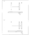
本発明の入力部付き表示装置について、図2の(a)・(b)および図3の(a)・(b)を用いて具体的に説明する。
本発明の入力部付き表示装置について、図2の(a)・(b)および図3の(a)・(b)を用いて具体的に説明する。
図2の(a)および図3の(a)・(b)に示すように、光の位置が(A)のときには、表示部において(A)の位置にポインタを表示する。しかし、表示部において(A)の位置にポインタを表示したときには、光の位置がすでに(B)に移動している。よって、光の位置と、表示部におけるポインタの位置とがずれるという状態になる。
そこで、図2の(b)に示すように、受光領域の形状によって、表示部におけるポインタの位置における補正値(補正量、移動量)を導き出し、当該ポインタの位置を、前回検知した光の位置と今回検知した光の位置とをつなぐベクトル方向に補正する。
図2の(b)に示すように、(A)、(B)および(C)の受光領域の形状は、(0)の受光領域の形状よりも小さいので、ポインタの位置を補正することになる。ここで、(A)の受光領域の形状は、(0)の受光領域の形状よりも小さいので、(0)と(A)との間では、移動量を増加させながら、すなわち加速度を上昇させながら光を移動させている。また、(B)の受光領域の形状は、(A)の受光領域の形状よりも大きいので、(A)と(B)との間では、移動量を減少させながら、すなわち加速度を低下させながら光を移動させている。(C)の受光領域の形状は、(B)の受光領域の形状よりも小さいので、(B)と(C)との間では、移動量を増加させながら、すなわち加速度を上昇させながら光を移動させている。
本発明の入力部付き表示装置において、光はシャッターを用いるので、ペン(光照射部)の移動量を増加させているほど、すなわち加速度が上昇しているほど、光のセンサ照度は小さくなる。
センサ画像(センサ位置およびセンサ形状、光の位置および受光領域の形状)は、60Hz、120Hz等のシャッタースピードによって取得されるので、ペン(光照射部)が止まっているほどセンサ形状(受光領域の形状)が大きくなる。よって、受光領域の形状が最大のものを静止時における受光領域の形状として、現時点での受光領域の形状が小さく、かつ光の位置(座標)が変化しているときに、ポインタの位置の補正を行う。
なお、本発明において、シャッタースピードは、60Hzまたは120Hzに限定されず、速度を上げればより滑らかになる。
要するに、現時点において検知した受光領域の形状が、前回検知したものよりも小さい場合には、移動量を増加させながら、すなわち加速度を上昇させながら光を移動させているということである。一方、現時点において検知した受光領域の形状が、前回検知したものよりも大きい場合には、移動量を減少させながら、すなわち加速度を低下させながら光を移動させているということである。
なお、本発明の入力部付き表示装置において、センサ画像(センサ位置およびセンサ形状、光の位置および受光領域の形状)は、履歴として保存され、ベクトルの算出時に参照される。
<本発明の入力部付き表示装置における入力部>
本発明の入力部付き表示装置における入力部は、光照射部からの照射光を検知する光検知部を有している。さらに、補正部は、光位置検知部および光形状検知部を有しており、当該光位置検知部が、上記光照射部から照射された光の位置を検知し、当該光形状検知部が、上記光照射部から光が照射されることによって形成される受光領域の形状を検知する。
本発明の入力部付き表示装置における入力部は、光照射部からの照射光を検知する光検知部を有している。さらに、補正部は、光位置検知部および光形状検知部を有しており、当該光位置検知部が、上記光照射部から照射された光の位置を検知し、当該光形状検知部が、上記光照射部から光が照射されることによって形成される受光領域の形状を検知する。
ここで、本発明における入力部としては、ペン型入力部、デジタイザ、タブレット等の入力部(入力装置)が挙げられる。
本発明の入力部付き表示装置における入力部は、上述した機能ブロック図の説明として記載した構成および機能以外は、従来公知の入力部の構成および機能を備えている。
<本発明の入力部付き表示装置における表示パネル>
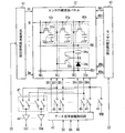
図4は、本発明における液晶パネル32の回路構成とその周辺回路の構成を示す回路ブロック図である。なお、図5はRGBのカラーフィルタがストライプ配列であり、青色絵素40bと同じ列にフォトダイオード39bが位置するように、すなわち、青色フィルタの背面にフォトダイオード39bが位置するように、光センサ30bを配置した場合の例である。なお、カラーフィルタの配列には、モザイク配列、デルタ配列等のように、上記ストライプ配列以外の配列を採用してもよい。
図4は、本発明における液晶パネル32の回路構成とその周辺回路の構成を示す回路ブロック図である。なお、図5はRGBのカラーフィルタがストライプ配列であり、青色絵素40bと同じ列にフォトダイオード39bが位置するように、すなわち、青色フィルタの背面にフォトダイオード39bが位置するように、光センサ30bを配置した場合の例である。なお、カラーフィルタの配列には、モザイク配列、デルタ配列等のように、上記ストライプ配列以外の配列を採用してもよい。
図4には図示しない、異なる画素においては、赤色絵素40rと同じ赤色フィルタの背面にフォトダイオード39rが位置するように、光センサ30rが配置されている。そして、青色絵素40bの光センサ30bと、赤色絵素40rの光センサ30rとは、ほぼ等しい数で規則的に配置されている。
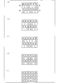
図5の(a)は、この場合における光センサ30の配置状態の一例を示す模式図である。この図において、「R」、「G」、「B」は、それぞれ赤色絵素、緑色絵素、青色絵素を示しており、「S」は、光センサを示している。画素4aおよび4cにおいては、青色絵素「B」に光センサ「S」が配置され、画素4bおよび4dにおいては、赤色絵素4bに光センサ「S」が配置される。
なお、図5の(a)においては、水平ラインごとに、光センサ「S」を配置する絵素を異なるものとしたが、配置規則はこれに限定されない。例えば、図5の(b)に示すように、光センサ「S」は、垂直ラインごとに、異なる絵素に配置されてもよい。また、図5の(c)に示すように、光センサ「S」は、となりあう画素ごとに、異なる絵素に配置されてもよい。さらに、図5の(d)または図5の(e)に示すように、光センサ「S」は、各絵素ごとに設けられてもよい。
ここで、緑色絵素4gに光センサ「S」が配置される場合、図4においては、緑色絵素40gと同じ緑色フィルタの背面にフォトダイオード39gが位置するように、光センサ30gが配置されている。そして、青色絵素40bの光センサ30bと、緑色絵素40gの光センサ30gとは、ほぼ等しい数で規則的に配置されている。
以下、青色絵素40bと同じ列の青色フィルタの背面にフォトダイオード39bが位置するように配置された光センサ30bが、センサ出力信号を出力する例について説明する。
図4に示すように、液晶パネル32は、m本の走査信号線G1~Gm、3n本のデータ信号線SR1~SRn、SG1~SGn、SB1~SBn、および(m×3n)個の画素回路40(40r,40g,40b)を備えるとともに、(m×n)個の光センサ30、m本のセンサ読み出し線RW1~RWm、およびm本のセンサリセット線RS1~RSmを備える。
走査信号線G1~Gmは、互いに平行に配置される。データ信号線SR1~SRn、SG1~SGn、SB1~SBnは、走査信号線G1~Gmと直交するように互いに平行に配置される。センサ読み出し線RW1~RWmとセンサリセット線RS1~RSmとは、走査信号線G1~Gmと平行に配置される。
画素回路40(40r,40g,40b)は、走査信号線G1~Gmとデータ信号線SR1~SRn、SG1~SGn、SB1~SBnとの交点近傍に1個ずつ設けられる。画素回路40は、列方向(図4では縦方向)にm個ずつ、行方向(図4では横方向)に3n個ずつ、全体として2次元状に配置される。
画素回路40は、設けられるカラーフィルタの色によって、赤色(R)画素回路40r、緑色(G)画素回路40gおよび青色(B)画素回路40bに分類される。3種類の画素回路40r,40g,40b(以下、それぞれを「絵素(サブ画素)」ともいう。)は、行方向に並べて配置され、3個で1個の画素を形成する。
画素回路40は、TFT(Thin Film Transistor)32aと液晶容量32bとを含んでいる。TFT32aのゲート端子は走査信号線Gi(iは1以上m以下の整数)に接続されており、ソース端子はデータ信号線SRj,SGj,SBj(jは1以上n以下の整数)のいずれかに接続され、ドレイン端子は液晶容量32bの一方の電極に接続される。液晶容量32bの他方の電極には、共通電極電圧が印加される。以下、緑色(G)画素回路40gに接続されたデータ信号線SG1~SGnをGデータ信号線、青色(B)画素回路40bに接続されたデータ信号線SB1~SBnをBデータ信号線という。なお、画素回路40は補助容量を含んでいてもよい。
画素回路40の光透過率(絵素の輝度)は、画素回路40に書き込まれた電圧によって定まる。走査信号線Giとデータ信号線SXj(XはR、G、Bのいずれか)とに接続された画素回路40にある電圧を書き込むためには、走査信号線Giにハイレベル電圧(TFT32aをオン状態にする電圧)を印加し、データ信号線SXjに書き込むべき電圧を印加すればよい。表示データDinに応じた電圧を画素回路40に書き込むことにより、絵素の輝度を所望のレベルに設定することができる。
光センサ30は、コンデンサ39a、フォトダイオード39bおよびセンサプリアンプ39cを含み、少なくとも、青色絵素40b(青色(B)画素回路40b)ごとに設けられる。
コンデンサ39aの一方の電極は、フォトダイオード39bのカソード端子に接続される(以下、この接続点を「節点A」という)。コンデンサ39aの他方の電極はセンサ読み出し線RWiに接続され、フォトダイオード39bのアノード端子はセンサリセット線RSiに接続される。センサプリアンプ39cは、ゲート端子が節点Aに接続され、ドレイン端子がBデータ信号線SBjに接続され、ソース端子がGデータ信号線SGjに接続されたTFTで構成される。
センサ読み出し線RWi、Bデータ信号線SBj等に接続された光センサ30で光量を検知するためには、図6に示すタイミングチャートのタイミングで、センサ読み出し線RWiとセンサリセット線RSiとに所定の電圧を印加し、Bデータ信号線SBjに電源電圧VDDを印加すればよい。センサ読み出し線RWiとセンサリセット線RSiとに所定の電圧を印加した後、フォトダイオード39bに光が入射すると、入射光量に応じた電流がフォトダイオード39bに流れ、節点Aの電圧は流れた電流の分だけ低下する。Bデータ信号線SBjに電源電圧VDDを印加すると、節点Aの電圧はセンサプリアンプ39cで増幅され、Gデータ信号線SGjには増幅後の電圧が出力される。したがって、Gデータ信号線SGjの電圧に基づき、光センサ30で検知された光量を求めることができる。
液晶パネル32の周辺には、走査信号線駆動回路41、データ信号線駆動回路42、センサ行駆動回路43、p個(pは1以上n以下の整数)のセンサ出力アンプ44および複数のスイッチ45~48が設けられる。走査信号線駆動回路41、データ信号線駆動回路42およびセンサ行駆動回路43は、図1ではパネル駆動回路31に相当する。
データ信号線駆動回路42は、3n本のデータ信号線に対応して3n個の出力端子を有する。Gデータ信号線SG1~SGnとこれに対応したn個の出力端子との間にはスイッチ45が1個ずつ設けられ、Bデータ信号線SB1~SBnとこれに対応したn個の出力端子との間にはスイッチ46が1個ずつ設けられる。Gデータ信号線SG1~SGnはp本ずつのグループに分けられ、グループ内でk番目(kは1以上p以下の整数)のGデータ信号線とk番目のセンサ出力アンプ44の入力端子との間にはスイッチ47が1個ずつ設けられる。Bデータ信号線SB1~SBnは、いずれもスイッチ48の一端に接続され、スイッチ48の他端には電源電圧VDDが印加される。図4に含まれるスイッチ45~47の個数はn個であり、スイッチ48の個数は1個である。
図4に示す回路は、表示期間とセンシング期間とで異なる動作を行う。表示期間では、スイッチ45,46はオン状態、スイッチ47、48はオフ状態となる。これに対してセンシング期間では、スイッチ45,46はオフ状態、スイッチ48はオン状態となり、スイッチ47はGデータ信号線SG1~SGnがグループごとに順にセンサ出力アンプ44の入力端子に接続されるように時分割でオン状態となる。
図6に示す表示期間では、走査信号線駆動回路41とデータ信号線駆動回路42とが動作する。走査信号線駆動回路41は、タイミング制御信号C1に従い、走査信号線G1~Gmの中から1ライン時間ごとに1本の走査信号線を選択し、選択した走査信号線にはハイレベル電圧を印加し、残りの走査信号線にはローレベル電圧を印加する。データ信号線駆動回路42は、表示データDR、DG、DBに基づき、データ信号線SR1~SRn、SG1~SGn、SB1~SBnを線順次方式で駆動する。
より詳細には、データ信号線駆動回路42は、表示データDR、DG、DBを少なくとも1行分ずつ記憶し、1ライン時間ごとに1行分の表示データに応じた電圧をデータ信号線SR1~SRn、SG1~SGn、SB1~SBnに印加する。なお、データ信号線駆動回路42は、データ信号線SR1~SRn、SG1~SGn、SB1~SBnを点順次方式で駆動してもよい。
図6に示すセンシング期間では、センサ行駆動回路43とセンサ出力アンプ44とが動作する。センサ行駆動回路43は、タイミング制御信号C2に従い、センサ読み出し線RW1~RWmとセンサリセット線RS1~RSmとの中から1ライン時間ごとに信号線を1本ずつ選択し、選択したセンサ読み出し線とセンサリセット線とには所定の読み出し用電圧とリセット用電圧とを印加し、それ以外の信号線には選択時と異なる電圧を印加する。なお、典型的には、表示期間とセンシング期間とでは、1ライン時間の長さは異なる。センサ出力アンプ44は、スイッチ47によって選択された電圧を増幅し、センサ出力信号SS1~SSpとして出力する。
なお、図6では、バックライト制御信号BCは、表示期間ではハイレベルになり、センシング期間ではローレベルになる。この場合、バックライト33は、表示期間では点灯し、センシング期間では消灯する。このため、フォトダイオード39bに対する、バックライト光の影響を減らすことができる。
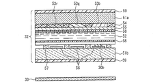
図7は、本発明における液晶パネル32の構成を示す断面図の一例である。液晶パネル32は、例えば、2枚のガラス基板51a,51bの間に液晶層52を挟み込んだ構造を有する。一方のガラス基板51aには、例えば、3色のカラーフィルタ53r,53g,53b、遮光膜54、対向電極55等が備えられており、他方のガラス基板51bには、例えば、画素電極56、データ信号線57、光センサ30等が設けられる。
光センサ30は、例えば青色カラーフィルタ53bを設けた画素電極56の近傍に設けられる。この場合、少なくとも、光センサ30のフォトダイオード39bは、カラーフィルタ53を透過した光を確実に受光させるために、カラーフィルタ53における中心の背面に配置されることが好ましい。
ガラス基板51a,51bの対向する面には配向膜58が設けられ、他方の面には偏光板59が設けられる。液晶パネル32の2枚の面のうち、ガラス基板51a側の面が表面になり、ガラス基板51b側の面が背面になる。バックライト33は、液晶パネル32の背面側に設けられる。
図8は、本発明における入力部付き表示装置50において、光が照射された位置を特定する処理の例を示すフローチャートである。図8に示す処理は、図1において示すMPU38によって1フレーム時間内において行われる。
A/D変換器36(図1を参照)は、液晶パネル32に内蔵された光センサ30が出力したアナログの出力信号SSをデジタル信号に変換する。
MPU38は、このデジタル信号をスキャン画像として取得する(ステップS74)。さらに、MPU38は、取得したスキャン画像に対して、画素位置を特定する処理を行う(ステップS75)。
例えば、図9の(a)は、画素数がm×nのスキャン画像の模式図である。図9の(a)に示すように、スキャン画像が所定閾値に基づいて二値化されている場合には、値が「1」である画素を光が照射された画素であると判断し、この画素における画素位置を特定する。図9の(a)では、画素位置(Xn-i,Ym-j)を特定する。
一方、図9の(b)は、複数の画素に対して光が照射された場合のスキャン画像を示している。この場合に特定される画素位置は、画素位置(Xn-i,Ym-j)の周囲にある8つの画素を含むものとなる。なお、図9の(b)のスキャン画像は、図5の(d)または図5の(e)に示す配置規則の場合に取得されるものである。
画素位置を特定すると、MPU38は、特定した画素に対応する画像内の座標(位置)を決定する処理を行う(ステップS76)。例えば、図9の(a)に示すように、特定した画素位置(Xn-i,Ym-j)に対応する座標を決定する。表示画像の画像解像度と液晶パネルの画面解像度が、「m×n」で一致する場合には、画素位置(Xn-i,Ym-j)を座標(位置)として決定する。なお、画像解像度と画面解像度とが一致しない場合には、座標変換を行って画素位置に対応する座標(位置)を決定すればよい。
なお、図9の(b)に示すように、画素位置(Xn-i,Ym-j)を含む8つの画素位置が特定された場合には、所定の規則に基づいて座標(位置)を決定すればよい。例えば、特定した画素の重心に最も近い画素に基づいて座標(位置)を決定すればよい。この場合、図9の(b)に示すように、値が「1」である複数の画素の重心にあたる画素位置(Xn-i,Ym-j)に基づいて対応する座標を決定することができる。なお、図9の(b)において、値が「1」の画素位置のすべてに対応する座標を座標(位置)として決定してもよい。
座標(位置)を決定すると、MPU38は、決定した座標における座標データを表示パネル中のパネル駆動回路31に対して出力する(ステップS77)。
本発明における入力部付き表示装置50において、照射された光の位置および形状を特定する処理は、以下のように行われる。この処理は、図1において示すMPU38によって行われる。
A/D変換器36(図1を参照)は、液晶パネル32に内蔵された光センサ30が出力したアナログの出力信号SSをデジタル信号に変換する。そして、MPU38は、このデジタル信号をセンサ画像として取得する。
これにより、MPU38は、取得したセンサ画像からエッジ抽出画像を特定する処理を行うことができる。
エッジ抽出画像を特定すると、MPU38は、特定したエッジ抽出画像に対応する移動方向を決定する処理を行う。移動方向を決定すると、MPU38は、決定した移動方向におけるデータを表示パネル中のパネル駆動回路31に対して出力する。
<本発明の入力部付き表示装置のプログラムによる実現例>
本発明の入力部付き表示装置の各ブロック(構成)は、ハードウェアロジックによって構成してもよいし、次のようにCPUを用いてソフトウェアによって実現してもよい。
本発明の入力部付き表示装置の各ブロック(構成)は、ハードウェアロジックによって構成してもよいし、次のようにCPUを用いてソフトウェアによって実現してもよい。
すなわち、本発明の入力部付き表示装置は、各機能を実現する制御プログラムの命令を実行するCPU(central processing unit)、上記プログラムを格納したROM(read only memory)、上記プログラムを展開するRAM(random access memory)、上記プログラムおよび各種データを格納するメモリ等の記憶装置(記録媒体)などを備えている。そして、本発明の目的は、上述した機能を実現するソフトウェアである上記入力部付き表示装置の制御プログラムのプログラムコード(実行形式プログラム、中間コードプログラム、ソースプログラム)をコンピュータで読み取り可能に記録した記録媒体を、上記入力部付き表示装置に供給し、そのコンピュータ(またはCPUやMPU)が記録媒体に記録されているプログラムコードを読み出し実行することによっても、達成可能である。
上記記録媒体としては、例えば、磁気テープやカセットテープ等のテープ系、フロッピー(登録商標)ディスク/ハードディスク等の磁気ディスクやCD-ROM/MO/MD/DVD/CD-R等の光ディスクを含むディスク系、ICカード(メモリカードを含む)/光カード等のカード系、あるいはマスクROM/EPROM/EEPROM/フラッシュROM等の半導体メモリ系などを用いることができる。
また、上記入力部付き表示装置を通信ネットワークと接続可能に構成し、上記プログラムコードを、通信ネットワークを介して供給してもよい。この通信ネットワークとしては、特に限定されず、例えば、インターネット、イントラネット、エキストラネット、LAN、ISDN、VAN、CATV通信網、仮想専用網(virtual private network)、電話回線網、移動体通信網、衛星通信網等が利用可能である。また、通信ネットワークを構成する伝送媒体としては、特に限定されず、例えば、IEEE1394、USB、電力線搬送、ケーブルTV回線、電話線、ADSL回線等の有線でも、IrDAやリモコンのような赤外線、Bluetooth(登録商標)、802.11無線、HDR、携帯電話網、衛星回線、地上波デジタル網等の無線でも利用可能である。なお、本発明は、上記プログラムコードが電子的な伝送で具現化された、搬送波に埋め込まれたコンピュータデータ信号の形態でも実現され得る。
<本発明の好ましい形態>
本発明の入力部付き表示装置は、上記ポインタ位置補正手段において、上記受光領域の面積が小さくなったときに、上記ポインタの位置における補正値を大きくすることが好ましい。
本発明の入力部付き表示装置は、上記ポインタ位置補正手段において、上記受光領域の面積が小さくなったときに、上記ポインタの位置における補正値を大きくすることが好ましい。
これにより、本発明の入力部付き表示装置は、補正後のポインタの位置を決定しやすいので、より一層精度良く操作することができる。
また、本発明の入力部付き表示装置は、上記ポインタ位置補正手段において、上記受光領域の面積の変化率に対する上記補正値が、次に示す式(1)
補正ベクトル = 移動ベクトル × 静止画像面積 / 実画像面積・・・(1)
によって規定されることが好ましい。
補正ベクトル = 移動ベクトル × 静止画像面積 / 実画像面積・・・(1)
によって規定されることが好ましい。
これにより、本発明の入力部付き表示装置は、補正前のポインタの位置からの補正量(移動量)を決定しやすいので、より一層容易に、かつ精度良く操作することができる。
本発明の入力部付き表示装置の制御方法は、上記ポインタ位置補正ステップにおいて、上記受光領域の面積が小さくなったときに、上記ポインタの位置における補正値を大きくすることが好ましい。
これにより、本発明の入力部付き表示装置の制御方法は、補正後のポインタの位置を決定しやすいので、より一層精度良く制御することができる。
また、本発明の入力部付き表示装置の制御方法は、上記ポインタ位置補正ステップにおいて、上記受光領域の面積の変化率に対する上記補正値が、次に示す式(1)
補正ベクトル = 移動ベクトル × 静止画像面積 / 実画像面積・・・(1)
によって規定されることが好ましい。
補正ベクトル = 移動ベクトル × 静止画像面積 / 実画像面積・・・(1)
によって規定されることが好ましい。
これにより、本発明の入力部付き表示装置の制御方法は、補正前のポインタの位置からの補正量(移動量)を決定しやすいので、より一層容易に、かつ精度良く制御することができる。
本発明の制御プログラムは、上記入力部付き表示装置を動作させる制御プログラムであって、コンピュータを上記の各部として機能させるためのものである。また、本発明の記録媒体は、上記制御プログラムを記録したコンピュータ読み取り可能なものである。
これにより、本発明の入力部付き表示装置は、コンピュータによって実現することが可能となる。
<その他の実施形態>
上述した具体的な実施形態は、あくまでも、本発明の技術内容を明らかにするものであって、そのような具体例にのみ限定して狭義に解釈されるべきものではなく、本発明の精神と次に記載する請求の範囲内において、いろいろと変更して実施することができるものである。
上述した具体的な実施形態は、あくまでも、本発明の技術内容を明らかにするものであって、そのような具体例にのみ限定して狭義に解釈されるべきものではなく、本発明の精神と次に記載する請求の範囲内において、いろいろと変更して実施することができるものである。
本発明の入力部付き表示装置は、パソコン、電子辞書、カーナビゲーション装置、携帯型情報端末、ゲーム機、電子黒板等の表示装置に利用することができる。
27 照度センサ
28 センサ位置検知部(光位置検知部)
29 センサ形状検知部(光形状検知部)
30 光センサ
31 パネル駆動回路
32 センサ内蔵液晶パネル
33 バックライト
34 バックライト電源回路
35 表示処理部
36 A/D変換器
37 D/S変換器
38 マイクロプロセッサユニット(MPU)
39 補正部
41 走査信号線駆動回路
42 データ信号線駆動回路
43 センサ行駆動回路
44 センサ出力アンプ
45 スイッチ
46 スイッチ
47 スイッチ
48 スイッチ
50 入力部付き表示装置
28 センサ位置検知部(光位置検知部)
29 センサ形状検知部(光形状検知部)
30 光センサ
31 パネル駆動回路
32 センサ内蔵液晶パネル
33 バックライト
34 バックライト電源回路
35 表示処理部
36 A/D変換器
37 D/S変換器
38 マイクロプロセッサユニット(MPU)
39 補正部
41 走査信号線駆動回路
42 データ信号線駆動回路
43 センサ行駆動回路
44 センサ出力アンプ
45 スイッチ
46 スイッチ
47 スイッチ
48 スイッチ
50 入力部付き表示装置
Claims (8)
- 主画像を表示する表示部と、該表示部上に表示されるべきポインタの位置情報を入力する入力部とを備えた入力部付き表示装置であって、
上記入力部は、光照射部からの照射光を検知する光検知部を有し、
補正部は、上記光照射部からの照射光の光軸の位置を検知する光位置検知部を有しており、上記ポインタの位置情報は、該光軸の位置として該光位置検知部に入力され、
上記補正部は、上記光照射部からの照射光を受容している受光領域の形状を検知する光形状検知部を有しており、
上記表示装置は、上記ポインタの位置を補正するポインタ位置補正手段をさらに備えており、
上記ポインタ位置補正手段は、上記光形状検知部が検知する、上記受光領域の形状が変化したときに、上記ポインタの位置情報を補正する
ことを特徴とする入力部付き表示装置。 - 上記ポインタ位置補正手段において、上記受光領域の面積が小さくなったときに、上記ポインタの位置における補正値を大きくすることを特徴とする請求項1に記載の入力部付き表示装置。
- 上記ポインタ位置補正手段において、上記受光領域の面積の変化率に対する上記補正値が、次に示す式(1)
補正ベクトル = 移動ベクトル × 静止画像面積 / 実画像面積・・・(1)
によって規定されることを特徴とする請求項2に記載の入力部付き表示装置。 - 表示部上に主画像を表示する表示ステップと、該表示部上に表示されるべきポインタの位置情報を入力する入力ステップとを含む入力部付き表示装置の制御方法であって、
上記入力ステップは、光照射ステップによって照射される照射光を検知する光検知ステップを有し、
補正ステップは、上記光照射ステップによって照射される照射光の光軸の位置を検知する光位置検知ステップを有しており、上記ポインタの位置情報は、該光軸の位置として該光位置検知ステップに入力され、
上記補正ステップは、上記光照射ステップによって照射される照射光を受容している受光領域の形状を検知する光形状検知ステップを有しており、
上記表示装置の制御方法は、上記ポインタの位置を補正するポインタ位置補正ステップをさらに含んでおり、
上記ポインタ位置補正ステップは、上記光形状検知ステップによって検知される、上記受光領域の形状が変化したときに、上記ポインタの位置情報を補正する
ことを特徴とする入力部付き表示装置の制御方法。 - 上記ポインタ位置補正ステップにおいて、上記受光領域の面積が小さくなったときに、上記ポインタの位置における補正値を大きくすることを特徴とする請求項4に記載の入力部付き表示装置の制御方法。
- 上記ポインタ位置補正ステップにおいて、上記受光領域の面積の変化率に対する上記補正値が、次に示す式(1)
補正ベクトル = 移動ベクトル × 静止画像面積 / 実画像面積・・・(1)
によって規定されることを特徴とする請求項5に記載の入力部付き表示装置の制御方法。 - 請求項1~3のいずれか1項に記載の入力部付き表示装置を動作させる制御プログラムであって、コンピュータを上記の各部として機能させるための制御プログラム。
- 請求項7に記載の制御プログラムを記録したコンピュータ読み取り可能な記録媒体。
Priority Applications (1)
| Application Number | Priority Date | Filing Date | Title |
|---|---|---|---|
| US13/638,385 US8743090B2 (en) | 2010-03-29 | 2010-11-24 | Display device with input unit, control method for same, control program and recording medium |
Applications Claiming Priority (2)
| Application Number | Priority Date | Filing Date | Title |
|---|---|---|---|
| JP2010-075141 | 2010-03-29 | ||
| JP2010075141 | 2010-03-29 |
Publications (1)
| Publication Number | Publication Date |
|---|---|
| WO2011121842A1 true WO2011121842A1 (ja) | 2011-10-06 |
Family
ID=44711616
Family Applications (1)
| Application Number | Title | Priority Date | Filing Date |
|---|---|---|---|
| PCT/JP2010/070927 Ceased WO2011121842A1 (ja) | 2010-03-29 | 2010-11-24 | 入力部付き表示装置およびその制御方法、並びに制御プログラムおよび記録媒体 |
Country Status (2)
| Country | Link |
|---|---|
| US (1) | US8743090B2 (ja) |
| WO (1) | WO2011121842A1 (ja) |
Families Citing this family (4)
| Publication number | Priority date | Publication date | Assignee | Title |
|---|---|---|---|---|
| EP3054409B1 (en) * | 2013-09-30 | 2023-01-25 | Kubota Corporation | Data collection device |
| US10136102B2 (en) | 2016-04-29 | 2018-11-20 | Microsoft Technology Licensing, Llc | Online conference broadcast using broadcast component |
| US11614806B1 (en) * | 2021-05-12 | 2023-03-28 | Apple Inc. | Input device with self-mixing interferometry sensors |
| US12353649B2 (en) | 2022-06-29 | 2025-07-08 | Apple Inc. | Input device with optical sensors |
Citations (2)
| Publication number | Priority date | Publication date | Assignee | Title |
|---|---|---|---|---|
| JPH09179687A (ja) * | 1995-12-27 | 1997-07-11 | Toshiba Corp | ポインティング・デバイスを使用した座標入力装置及びそのカーソル移動制御方法 |
| JP2002182839A (ja) * | 2000-12-12 | 2002-06-28 | Semiconductor Energy Lab Co Ltd | 情報装置 |
Family Cites Families (9)
| Publication number | Priority date | Publication date | Assignee | Title |
|---|---|---|---|---|
| JP3606969B2 (ja) | 1995-10-18 | 2005-01-05 | 株式会社リコー | ペン型入力装置 |
| US7626575B2 (en) * | 2003-03-28 | 2009-12-01 | Samsung Electronics Co., Ltd. | Light pen |
| JP2005346453A (ja) | 2004-06-03 | 2005-12-15 | Ricoh Co Ltd | 画像表示装置 |
| US7791597B2 (en) * | 2006-02-10 | 2010-09-07 | Microsoft Corporation | Uniquely identifiable inking instruments |
| JP2007241410A (ja) | 2006-03-06 | 2007-09-20 | Pioneer Electronic Corp | 表示装置及び表示制御方法 |
| KR101365491B1 (ko) * | 2006-11-17 | 2014-02-24 | 삼성디스플레이 주식회사 | 디스플레이장치 |
| JP4991458B2 (ja) | 2007-09-04 | 2012-08-01 | キヤノン株式会社 | 画像表示装置及びその制御方法 |
| CN102027439A (zh) | 2008-05-12 | 2011-04-20 | 夏普株式会社 | 显示装置和控制方法 |
| WO2011102038A1 (ja) | 2010-02-16 | 2011-08-25 | シャープ株式会社 | タッチパネル付き表示装置およびその制御方法、並びに制御プログラムおよび記録媒体 |
-
2010
- 2010-11-24 WO PCT/JP2010/070927 patent/WO2011121842A1/ja not_active Ceased
- 2010-11-24 US US13/638,385 patent/US8743090B2/en not_active Expired - Fee Related
Patent Citations (2)
| Publication number | Priority date | Publication date | Assignee | Title |
|---|---|---|---|---|
| JPH09179687A (ja) * | 1995-12-27 | 1997-07-11 | Toshiba Corp | ポインティング・デバイスを使用した座標入力装置及びそのカーソル移動制御方法 |
| JP2002182839A (ja) * | 2000-12-12 | 2002-06-28 | Semiconductor Energy Lab Co Ltd | 情報装置 |
Also Published As
| Publication number | Publication date |
|---|---|
| US20130021244A1 (en) | 2013-01-24 |
| US8743090B2 (en) | 2014-06-03 |
Similar Documents
| Publication | Publication Date | Title |
|---|---|---|
| US9015625B2 (en) | Electronic device, method of selecting menu, and program for selecting menu | |
| US20120319977A1 (en) | Display device with touch panel, control method therefor, control program, and recording medium | |
| US20060214892A1 (en) | Display device and display method | |
| JPWO2009104667A1 (ja) | 光センサ付き表示装置 | |
| JP2008305087A (ja) | 表示装置 | |
| JP5367339B2 (ja) | メニュー表示装置、メニュー表示装置の制御方法、およびメニュー表示プログラム | |
| CN102043545B (zh) | 信息输入装置、信息输入方法以及电子设备 | |
| US20100271335A1 (en) | Display device having optical sensors | |
| US20120212412A1 (en) | Pointing device | |
| JP2010140300A (ja) | 表示装置、制御方法、制御プログラムおよび記録媒体 | |
| JP5322163B2 (ja) | 表示装置、表示方法、および表示プログラム | |
| JP5095574B2 (ja) | 画像表示/像検知装置、画像表示方法、画像表示プログラムおよび当該プログラムを記録した記録媒体 | |
| JP2011008424A (ja) | 電子機器、動作モード設定方法、およびプログラム | |
| WO2010100798A1 (ja) | 表示装置、テレビ受信装置およびポインティングシステム | |
| JP5303785B2 (ja) | 表示装置、表示方法、および表示プログラム | |
| WO2011121842A1 (ja) | 入力部付き表示装置およびその制御方法、並びに制御プログラムおよび記録媒体 | |
| JP2010122972A (ja) | 画像表示/検出装置、選択方法、及び、プログラム | |
| WO2010150572A1 (ja) | 光センサ付き表示装置 | |
| JP5306780B2 (ja) | 入力装置 | |
| JP5254753B2 (ja) | 数値入力装置、数値入力方法、数値入力プログラム、およびコンピュータ読み取り可能な記録媒体 | |
| US20120256881A1 (en) | Display device, display method, display program, recording medium | |
| JP2010109467A (ja) | 画像表示/像検知装置 | |
| JP5567776B2 (ja) | 色検出/色出力装置、色検出/色出力プログラム及びコンピュータ読み取り可能な記録媒体、並びに色検出/色出力方法 | |
| JP5380729B2 (ja) | 電子機器、表示制御方法、およびプログラム | |
| JP2010117841A (ja) | 像検知装置、入力位置の認識方法、およびプログラム |
Legal Events
| Date | Code | Title | Description |
|---|---|---|---|
| 121 | Ep: the epo has been informed by wipo that ep was designated in this application |
Ref document number: 10849013 Country of ref document: EP Kind code of ref document: A1 |
|
| WWE | Wipo information: entry into national phase |
Ref document number: 13638385 Country of ref document: US |
|
| NENP | Non-entry into the national phase |
Ref country code: DE |
|
| 122 | Ep: pct application non-entry in european phase |
Ref document number: 10849013 Country of ref document: EP Kind code of ref document: A1 |
|
| NENP | Non-entry into the national phase |
Ref country code: JP |