WO2011121707A1 - 3次元放射線位置検出器、及び、その検出位置特定方法 - Google Patents
3次元放射線位置検出器、及び、その検出位置特定方法 Download PDFInfo
- Publication number
- WO2011121707A1 WO2011121707A1 PCT/JP2010/055588 JP2010055588W WO2011121707A1 WO 2011121707 A1 WO2011121707 A1 WO 2011121707A1 JP 2010055588 W JP2010055588 W JP 2010055588W WO 2011121707 A1 WO2011121707 A1 WO 2011121707A1
- Authority
- WO
- WIPO (PCT)
- Prior art keywords
- scintillator
- light
- dimensional radiation
- light receiving
- position detector
- Prior art date
- Legal status (The legal status is an assumption and is not a legal conclusion. Google has not performed a legal analysis and makes no representation as to the accuracy of the status listed.)
- Ceased
Links
Images








Classifications
-
- G—PHYSICS
- G01—MEASURING; TESTING
- G01T—MEASUREMENT OF NUCLEAR OR X-RADIATION
- G01T1/00—Measuring X-radiation, gamma radiation, corpuscular radiation, or cosmic radiation
- G01T1/16—Measuring radiation intensity
- G01T1/161—Applications in the field of nuclear medicine, e.g. in vivo counting
- G01T1/164—Scintigraphy
- G01T1/1641—Static instruments for imaging the distribution of radioactivity in one or two dimensions using one or several scintillating elements; Radio-isotope cameras
- G01T1/1644—Static instruments for imaging the distribution of radioactivity in one or two dimensions using one or several scintillating elements; Radio-isotope cameras using an array of optically separate scintillation elements permitting direct location of scintillations
Definitions
- the present invention relates to a three-dimensional radiation position detector and a detection position specifying method thereof, and in particular, a light receiving element is three-dimensionally arranged on the surface of a cubic or cuboid scintillator block that emits light when absorbing radiation, Even when the internal scintillator element is smaller than the light receiving element, which is suitable for use in a three-dimensional radiation position detector that can three-dimensionally read the position where the radiation is detected in the detector, the position discrimination performance can be improved.
- the present invention relates to a three-dimensional radiation position detector capable of preventing deterioration and a detection position specifying method thereof.
- a photomultiplier tube has been used as a light receiving element for a PET detector.
- the PMT When the PMT is located on the surface of the subject (referred to as the upper surface of the scintillator block) when incorporated in the PET apparatus, the occupied space not only infringe the detection area, but also a scatterer during radiation detection. It becomes.
- the PMT 12 is bonded only to the surface opposite to the subject (referred to as the lower surface of the scintillator block 10).
- the two-dimensional localization of the place where the radiation is absorbed in the scintillator block 10 is performed by combining a plurality of PMTs or position-discriminating type PMTs (PS-PMT) 12 on the lower surface and calculating an angel calculation of the signal, that is, calculating the center of gravity. This is performed by the same position calculation as that obtained.
- a response corresponding to the absorbed position appears on the two-dimensional (2D) position histogram representing the result of the anger calculation.
- FIG. As illustrated in (b), the response of each element appears discontinuously.
- a semiconductor light receiving element having a small volume does not become a scatterer even if the light receiving element is arranged on the upper surface of the detector. 2 (a) and 2 (b), the light receiving elements (the photodiode (PD) 14 on the upper surface side and the lower surface side in FIG. 2 (a)) are arranged on the upper and lower surfaces of the element arrangement of the scintillator block 10. PS-PMT12 of FIG. 2 and the position discrimination type APD 16) in the upper and lower surfaces in FIG.
- Non-Patent Documents 1 and 2B are combined, and a DOI detection method (see Non-Patent Documents 1 and 2) for obtaining DOI information by the ratio of these signals,
- a study of a DOI detector in which a light receiving element (APD 16) is coupled to a side surface and a position in the DOI direction is specified from the signal has been made (see Non-Patent Document 3).
- the scintillator light is efficiently combined because the wide surface of the scintillator element is coupled to the light receiving element.
- the loss of light quantity obtained is small, the packing fraction when the PET apparatus is made by the amount of the light receiving element is reduced.
- the inventors have studied a DOI detector in which semiconductor light-receiving elements 18 are three-dimensionally arranged on the surface of a three-dimensional array 10A of small scintillator elements 10C (patent) Reference 1 and Non-Patent Document 4).
- a DOI detector in which semiconductor light-receiving elements 18 are three-dimensionally arranged on the surface of a three-dimensional array 10A of small scintillator elements 10C (patent) Reference 1 and Non-Patent Document 4).
- the light receiving elements are arranged on the xy plane, the xz plane, and the yz plane, respectively.
- the component, y component, and z component are determined.
- Another group has proposed a detector structure in which a block is composed of one large scintillator having no optical discontinuity and a light receiving element is arranged in each of the xy plane, the xz plane, and the yz plane.
- a light receiving element that is not a position discrimination type, and a method of specifying the radiation absorption position by simulation is considered (see Non-Patent Document 5).
- the other is a comparison of detector performance due to the difference in the arrangement of the light receiving elements. In the simulation, it is used as an example of the light receiving element arrangement (see Non-Patent Document 6).
- the scintillator block 10 in which the light receiving elements are arranged is constituted by a three-dimensional array 10A of small scintillator elements 10C, as shown in FIG. 3A, the scintillation light emitted by the element 10C absorbing radiation is Due to the optical discontinuity characteristic between the element and the inter-element material, there is a tendency to propagate along the column including the element that emits light (the column in the front-rear, left-right, and vertical directions).
- the scintillator block 10 is composed of one large cubic scintillator 10B having no optical discontinuity, as shown in FIG. To spread.
- the light spreading in the scintillator block 10 constituted by a three-dimensional element array is propagated unevenly in the upper, lower, left and right element rows of the emitted scintillator elements. It has the characteristics.
- PS-PMT which has been used as a light receiving element in the past, has a series of window glass on the light receiving surface, where light spreads so that light incident between sampling points can be received, whereas a semiconductor light receiving element is a light receiving element There is a dead zone in between.
- each scintillator element row is coupled to any one of the semiconductor light receiving elements, and light is emitted from any one of the scintillator elements up and down, left and right, and both ends of the front and rear element rows.
- the number of semiconductor light receiving elements is reduced, there is a case where optical coupling is not performed with both ends of the element row, and the position discrimination accuracy of the row may be deteriorated.
- the light receiving element is larger than the scintillator element and one light receiving element covers the entire end face of the plurality of element rows, if the light spread is poor, a signal is output to the nearest different light receiving elements in the element rows. Therefore, it is difficult to distinguish between these element arrays in signal position calculation.
- the above two problems are usually identified by inserting a light guide between the light receiving element and the scintillator block to create a light spread just before light reception, thereby minimizing positional information degradation and identifying the light emitting scintillator element array. Can be made possible.
- As the material of the light guide resin such as acrylic or glass is used.
- the light guide 20 itself hardly absorbs radiation and does not emit light even if it absorbs radiation.
- a light receiving element (especially a thin semiconductor light receiving element) 18 is coupled to a plurality of surfaces of the scintillator block 10
- the size of the light guide 20 when incorporated in the PET apparatus 100 as shown in the upper right part of FIG. Becomes a radiation insensitive region, leading to a decrease in sensitivity of the apparatus.
- the scintillation light is not limited by the light emitting point as shown in FIG. spread. Therefore, there is no problem in the detector structure capable of receiving light over the entire surface of the scintillator block 10, but when a part of the surface is a dead area of the light receiving element, if the dead area is covered with a reflective material to prevent light loss, Since reflected light travels without restriction, position information is lost by that amount and position accuracy is deteriorated. To prevent this, if the insensitive area is covered with a light absorbing material such as black paper, the position information is deteriorated due to light loss. .
- Non-Patent Document 7 As an attempt to suppress the degradation of the position resolution when the thickness of the scintillator block is increased, a device (see Non-Patent Document 8) in which the surface facing the light receiving surface of the scintillator block is a plurality of triangular peaks, or the scintillator block Has been made (see Non-Patent Document 9).
- the light receiving surface is one surface of the scintillator block.
- the present invention has been made in view of the above circumstances, and even when the internal scintillator element is smaller than the light receiving element, a three-dimensional radiation position detector capable of preventing deterioration of position discrimination performance, and the It is an object of the present invention to provide a detection position specifying method.
- a three-dimensional radiation position detector in which a light receiving element is three-dimensionally arranged on the surface of the scintillator block and the position where the radiation is detected in the detector can be read out three-dimensionally.
- the scintillation light from the adjacent scintillator element 10C may be received by the light receiving element 18 with substantially the same distribution.
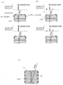
- the scintillator plate 11 is provided between the scintillator block 10 and the light receiving element 18 to spread the scintillation light to the nearby light receiving element 18 so that the scintillator plate 11 is not present.
- the element can be identified based on the signal position calculation result.
- the scintillator block is composed of one large scintillator. Furthermore, the inner scintillator and the outer scintillator plate can be formed in the same scintillator block.
- the present invention has been made on the basis of the above-described knowledge, and has a central portion having an optically discontinuous region for restricting the light diffusion direction and guiding it in the three-axis direction, and outside the central portion.
- a scintillator block that includes an outer portion that is disposed and does not limit the direction of light diffusion;
- a light receiving element disposed on at least two surfaces of the outer periphery of the scintillator block,
- the outer portion and the light receiving element can be disposed on all surfaces of the outer periphery of the scintillator block.
- the outer portion and the light receiving element can be disposed on a part of the outer periphery of the scintillator block.
- the central portion may be formed by arranging a plurality of scintillator elements, and the outer portion may be a scintillator plate.
- the central portion may be a single scintillator having an optically discontinuous region formed therein, and the outer portion may be a scintillator plate.
- a reflective material can be inserted into the contact surface between the scintillator plates.
- the scintillator plates can be prevented from contacting each other.
- central portion and the outer portion can be formed of a single scintillator.
- the present invention is also the above-described three-dimensional radiation position detector, wherein the detection position of the three-dimensional radiation position detector using different types of scintillators in the central part and the outer part is specified. Based on the waveform discrimination of the received light signal, it is identified whether the light is received by the central part or the outer part, In the case of light reception by the central part, the position calculation for the central part is performed, In the case of light reception by the outer portion, a detection position specifying method of a three-dimensional radiation position detector is provided, wherein position calculation for the outer portion is performed.
- the position calculation for the central part is performed, In the case of light reception by the outer portion, a detection position specifying method of a three-dimensional radiation position detector is provided, wherein position calculation for the outer portion is performed.
- the scintillator block is divided into a three-dimensional array 10A of small scintillator elements, or a central portion composed of one large scintillator 10B having an optical discontinuous surface formed therein by, for example, laser processing, and a light guide. It is possible to improve the resolution of the radiation detection position by controlling the spread of light.
- the present invention does not require a high packing fraction unlike the PET detector, and can be applied to a radiation detector in which light receiving elements other than semiconductor light receiving elements such as PS-PMT are arranged in a three-dimensional array.
- A The perspective view which shows an example of the conventional radiation detector
- A A perspective view showing a light propagation state in a scintillator block constituted by a three-dimensional array of fine scintillator elements, and (b) a light spread in a scintillator block constituted by one large scintillator.
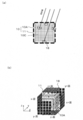
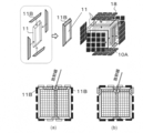
- Figure showing Cross-sectional view for explaining conventional problems Diagram showing the principle of the present invention The (a) sectional view and (b) exploded perspective view showing composition of a 1st embodiment of a radiation detector concerning the present invention.
- Sectional drawing which shows the state which integrated 1st Embodiment in PET apparatus Sectional drawing which shows the various modifications of 1st Embodiment Sectional drawing which shows the structure of 2nd Embodiment of this invention. Sectional drawing which shows the structure of 3rd Embodiment of this invention. Sectional drawing which shows the structure and effect
- a flow chart showing a specific example Flow chart showing an example of a radiation detection position specifying method for discriminating a central portion and an outer portion of a scintillator block by intensity analysis of a light receiving element signal using the present invention.
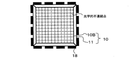
- a scintillator block 10 has a three-dimensional array of small scintillator elements 10C as shown in FIGS. 10A and the outer part which consists of the scintillator plate 11 which does not restrict
- the internal scintillator element 10C is smaller than the light receiving element 18, and one light receiving element 18 covers all end faces of a plurality of element rows.
- the scintillator plate 11 functions like a light receiving glass or light guide for PS-PMT with respect to light emitted from the scintillator elements 10C in the scintillator element array 10A. Whether the rows are located between the semiconductor light receiving elements 18 or the plurality of element rows are on the same light receiving element, the spread of light on the scintillator plate 11 prevents the position discrimination ability from being greatly deteriorated. it can. Further, since the scintillator plate 11 is a part of the scintillator block 10 and can detect radiation, there is no decrease in sensitivity when incorporated in the PET apparatus 100 as shown in FIG.
- the scintillator block 10 of the present invention has a structure in which the scintillator element 10C and the scintillator plate 11 improve the position discrimination performance of each other.
- the scintillator element array inside the scintillator block 10 includes not only the array of individual elements 10C as in the first embodiment, but also a laser beam in a large lump scintillator 10B as in the second embodiment shown in FIG. The same effect can be expected even when the wall surface formed of optical discontinuities such as microcracks is processed (see Patent Document 2).
- a central portion having an optical discontinuity similar to that of the scintillator 10B and an outer portion similar to that of the scintillator plate 11 inside a larger lump scintillator 10D is also possible to make them separately.
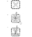
- the third embodiment may be further improved so that the discontinuity of the central portion is not uniform as in the fourth embodiment shown in FIG. Examples of the state of light when radiation is incident on the fourth embodiment are shown in FIGS.
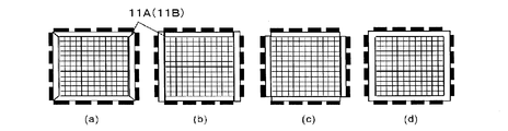
- the cross-sectional shape of the scintillator plate 11 for example, a trapezoidal shape having a 45 ° inclined surface shown in FIG. 12 (a), a rectangular shape shown in FIGS. 12 (b) to 12 (d). It may be a shape or another shape.
- the contact surface 11A between the plates there is no limitation on the contact surface 11A between the plates.
- optical grease is used as the reflector 11B, or between the plates as shown in FIG. 12 (c). It is good also as a non-contact by releasing.
- the central portion and the outer portion of the scintillator block can be identified by waveform discrimination using different types of scintillators.
- the same scintillator is used also in the third and fourth embodiments and the first and second embodiments, for example, the reflecting material 11B is inserted into the contact surface 11A of the plate 11 in FIGS. 12 (a) and 12 (b).
- the structure and the structure in which the contact surface in FIG. 12C is separated can be distinguished from each other because the light receiving elements that output signals are different.
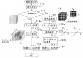
- FIG. 14 shows an outline of the detection position specifying method in the case where the central portion and the outer plate portion are identified by the waveform discrimination method.
- anger calculation of the light receiving element signal (step 114a), lookup table (LUT) reference (step 114b), maximum likelihood estimation method, etc. can be considered.
- the anger calculation (step 122a) of the light receiving element signal takes into account the correction (linear correction) of the degradation of the end position resolution caused by a series of scintillators (steps 122b and 122c) or the maximum likelihood estimation method. And so on.
- FIG. 16 shows an outline of the detection position specifying method in the case where the portion where the radiation is detected by the output light receiving element is determined. After analyzing the intensity ratio of the light receiving element signal in step 130 and identifying whether it is the central portion or the outer portion in step 132, the radiation detection position can be specified by the same method as in FIG.
- steps 150 and 152 anger calculation and LUT reference similar to steps 114a and 114b in FIG. 15 are performed to obtain the light emission position.
- the position calculation for the outer portion can be performed.
- the radiation detector and the position detection method thereof according to the present invention can be used for a radiation detector such as a PET detector, a SPECT detector, and a gamma camera.
Landscapes
- Physics & Mathematics (AREA)
- Health & Medical Sciences (AREA)
- Engineering & Computer Science (AREA)
- Biomedical Technology (AREA)
- General Health & Medical Sciences (AREA)
- Medical Informatics (AREA)
- Nuclear Medicine, Radiotherapy & Molecular Imaging (AREA)
- Optics & Photonics (AREA)
- Life Sciences & Earth Sciences (AREA)
- General Physics & Mathematics (AREA)
- High Energy & Nuclear Physics (AREA)
- Molecular Biology (AREA)
- Spectroscopy & Molecular Physics (AREA)
- Nuclear Medicine (AREA)
- Measurement Of Radiation (AREA)
Abstract
Description
該シンチレータ・ブロック外周の少なくとも2面に配設された受光素子とを備え、
発光位置を3次元で特定することを特徴とする3次元放射線位置検出器により、前記課題を解決したものである。
受光信号の波形弁別により、中央部分による受光か、外側部分による受光かを識別し、
中央部分による受光の場合は、中央部分用の位置演算を行ない、
外側部分による受光の場合は、外側部分用の位置演算を行なうことを特徴とする3次元放射線位置検出器の検出位置特定方法を提供するものである。
それぞれの受光素子から出る受光信号の強度比が異なることにより、中央部分による受光か、外側部分による受光かを識別し、
中央部分による受光の場合は、中央部分用の位置演算を行ない、
外側部分による受光の場合は、外側部分用の位置演算を行なうことを特徴とする3次元放射線位置検出器の検出位置特定方法を提供するものである。
10A…3次元配列
10B、10D…シンチレータ
10C…シンチレータ素子
11…シンチレータ・プレート
11A…接触部
11B…反射材
18…半導体受光素子
Claims (10)
- 光の拡散方向を制限して3軸方向に導くための、光学的に不連続な領域を有する中央部分、及び、該中央部分の外側に配設された、光の拡散方向を制限しない外側部分を含むシンチレータ・ブロックと、
該シンチレータ・ブロック外周の少なくとも2面に配設された受光素子とを備え、
発光位置を3次元で特定することを特徴とする3次元放射線位置検出器。 - 前記外側部分及び受光素子が、シンチレータ・ブロックの外周の全ての面に配設されている請求項1に記載の3次元放射線位置検出器。
- 前記外側部分及び受光素子が、シンチレータ・ブロックの外周の一部の面に配設されている請求項1に記載の3次元放射線位置検出器。
- 前記中央部分が、複数のシンチレータ素子が配列されてなり、前記外側部分が、シンチレータ・プレートでなる請求項1乃至3のいずれかに記載の3次元放射線位置検出器。
- 前記中央部分が、光学的に不連続な領域が内部に形成された一塊のシンチレータでなり、前記外側部分が、シンチレータ・プレートでなる請求項1乃至3のいずれかに記載の3次元放射線位置検出器。
- 前記シンチレータ・プレート同士の接触面に反射材が挿入されている請求項4又は5に記載の3次元放射線位置検出器。
- 前記シンチレータ・プレート同士が接触しないようにされている請求項4又は5に記載の3次元放射線位置検出器。
- 前記中央部分及び外側部分が、単一のシンチレータでなる請求項1乃至3のいずれかに記載の3次元放射線位置検出器。
- 請求項4乃至7のいずれかに記載の3次元放射線位置検出器であって、中央部分と外側部分に異なる種類のシンチレータを用いた3次元放射線位置検出器の検出位置特定に際して、
受光信号の波形弁別により、中央部分による受光か、外側部分による受光かを識別し、
中央部分による受光の場合は、中央部分用の位置演算を行ない、
外側部分による受光の場合は、外側部分用の位置演算を行なうことを特徴とする3次元放射線位置検出器の検出位置特定方法。 - 請求項1乃至8のいずれかに記載の3次元放射線位置検出器の検出位置特定に際して、
それぞれの受光素子から出る受光信号の強度比が異なることにより、中央部分による受光か、外側部分による受光かを識別し、
中央部分による受光の場合は、中央部分用の位置演算を行ない、
外側部分による受光の場合は、外側部分用の位置演算を行なうことを特徴とする3次元放射線位置検出器の検出位置特定方法。
Priority Applications (3)
| Application Number | Priority Date | Filing Date | Title |
|---|---|---|---|
| US13/636,936 US8933410B2 (en) | 2010-03-29 | 2010-03-29 | Three-dimensional position-sensitive radiation detector and method of identifying radiation detected positions therein |
| PCT/JP2010/055588 WO2011121707A1 (ja) | 2010-03-29 | 2010-03-29 | 3次元放射線位置検出器、及び、その検出位置特定方法 |
| JP2012507937A JP5630756B2 (ja) | 2010-03-29 | 2010-03-29 | 3次元放射線位置検出器、及び、その検出位置特定方法 |
Applications Claiming Priority (1)
| Application Number | Priority Date | Filing Date | Title |
|---|---|---|---|
| PCT/JP2010/055588 WO2011121707A1 (ja) | 2010-03-29 | 2010-03-29 | 3次元放射線位置検出器、及び、その検出位置特定方法 |
Publications (1)
| Publication Number | Publication Date |
|---|---|
| WO2011121707A1 true WO2011121707A1 (ja) | 2011-10-06 |
Family
ID=44711502
Family Applications (1)
| Application Number | Title | Priority Date | Filing Date |
|---|---|---|---|
| PCT/JP2010/055588 Ceased WO2011121707A1 (ja) | 2010-03-29 | 2010-03-29 | 3次元放射線位置検出器、及び、その検出位置特定方法 |
Country Status (3)
| Country | Link |
|---|---|
| US (1) | US8933410B2 (ja) |
| JP (1) | JP5630756B2 (ja) |
| WO (1) | WO2011121707A1 (ja) |
Cited By (7)
| Publication number | Priority date | Publication date | Assignee | Title |
|---|---|---|---|---|
| US20130009067A1 (en) * | 2011-07-06 | 2013-01-10 | Siemens Aktiengesellschaft | Positron Emission Tomography Detector Based on Monolithic Scintillator Crystal |
| WO2013099162A1 (ja) * | 2011-12-28 | 2013-07-04 | 学校法人早稲田大学 | 放射線検出器 |
| JP2014020843A (ja) * | 2012-07-13 | 2014-02-03 | Waseda Univ | コンプトンカメラ |
| JP2014215145A (ja) * | 2013-04-25 | 2014-11-17 | 国立大学法人東京大学 | 光子検出装置および放射線測定装置 |
| US10345457B2 (en) | 2015-09-02 | 2019-07-09 | National University Corporation Hokkaido University | Scintillation light detecting device and radiation detecting device |
| JP2022519397A (ja) * | 2019-02-15 | 2022-03-24 | ザ リサーチ ファウンデイション フォー ザ ステイト ユニヴァーシティ オブ ニューヨーク | 擬角柱光ガイドアレイを有する高分解能深さ符号化pet検出器 |
| KR20230004060A (ko) * | 2021-06-30 | 2023-01-06 | 서강대학교산학협력단 | 다층 평판형 섬광체를 이용한 양전자 방출 단층 촬영 장치 및 방법 |
Families Citing this family (12)
| Publication number | Priority date | Publication date | Assignee | Title |
|---|---|---|---|---|
| US10684380B2 (en) * | 2008-05-22 | 2020-06-16 | W. Davis Lee | Multiple scintillation detector array imaging apparatus and method of use thereof |
| US9612344B2 (en) * | 2014-01-28 | 2017-04-04 | Theta Point, LLC | Positron emission tomography and single photon emission computed tomography based on intensity attenuation shadowing methods and effects |
| US10094937B2 (en) * | 2015-01-30 | 2018-10-09 | Hamamatsu Photonics K.K. | Radiation detector |
| CN107735694B (zh) * | 2015-05-01 | 2020-05-12 | 得克萨斯大学体系董事会 | 用于使用二分感测的交互深度正电子断层扫描检测器的装置和方法 |
| WO2017181112A2 (en) * | 2016-04-15 | 2017-10-19 | Saint-Gobain Ceramics & Plastics, Inc | Photosensors arranged on a surface of a scintillator |
| US11385362B2 (en) * | 2016-10-28 | 2022-07-12 | Arizona Board Of Regents On Behalf Of The University Of Arizona | Scintillation detector and associated scintillation detector ring and method |
| CN107121692B (zh) * | 2017-06-05 | 2019-07-26 | 中派科技(深圳)有限责任公司 | 检测器和具有该检测器的发射成像设备 |
| WO2019000389A1 (en) | 2017-06-30 | 2019-01-03 | Shanghai United Imaging Healthcare Co., Ltd. | SYSTEM AND METHOD FOR POSITRON EMISSION TOMOGRAPHY |
| US10267931B1 (en) * | 2018-02-06 | 2019-04-23 | Siemens Medical Solutions Usa, Inc. | Radiation detector capable of measuring depth-of-interaction |
| IT201900010638A1 (it) * | 2019-07-02 | 2021-01-02 | St Microelectronics Srl | Rilevatore di radiazione a scintillatore e dosimetro corrispondente |
| EP3998499A4 (en) * | 2019-07-08 | 2023-06-14 | National Institutes for Quantum Science and Technology | RADIATION POSITION DETECTOR |
| WO2023205597A2 (en) * | 2022-04-22 | 2023-10-26 | Stuart Miller | High-resolution photon-counting radiographic imaging detector |
Citations (4)
| Publication number | Priority date | Publication date | Assignee | Title |
|---|---|---|---|---|
| JP2005533245A (ja) * | 2002-07-17 | 2005-11-04 | ヨーロピアン オーガナイゼーション フォー ニュークリア リサーチ | 陽電子放射断層撮影(pet)用及び単一光子放射コンピュータ断層撮影(spect)用のガンマ線検出器 |
| JP2009506316A (ja) * | 2005-08-26 | 2009-02-12 | コーニンクレッカ フィリップス エレクトロニクス エヌ ヴィ | 高解像度医療撮像検出器 |
| JP2009121929A (ja) * | 2007-11-14 | 2009-06-04 | Hamamatsu Photonics Kk | 放射線位置検出器 |
| JP2009270971A (ja) * | 2008-05-08 | 2009-11-19 | Hamamatsu Photonics Kk | シンチレータの製造方法および放射線位置検出器 |
-
2010
- 2010-03-29 JP JP2012507937A patent/JP5630756B2/ja not_active Expired - Fee Related
- 2010-03-29 US US13/636,936 patent/US8933410B2/en not_active Expired - Fee Related
- 2010-03-29 WO PCT/JP2010/055588 patent/WO2011121707A1/ja not_active Ceased
Patent Citations (4)
| Publication number | Priority date | Publication date | Assignee | Title |
|---|---|---|---|---|
| JP2005533245A (ja) * | 2002-07-17 | 2005-11-04 | ヨーロピアン オーガナイゼーション フォー ニュークリア リサーチ | 陽電子放射断層撮影(pet)用及び単一光子放射コンピュータ断層撮影(spect)用のガンマ線検出器 |
| JP2009506316A (ja) * | 2005-08-26 | 2009-02-12 | コーニンクレッカ フィリップス エレクトロニクス エヌ ヴィ | 高解像度医療撮像検出器 |
| JP2009121929A (ja) * | 2007-11-14 | 2009-06-04 | Hamamatsu Photonics Kk | 放射線位置検出器 |
| JP2009270971A (ja) * | 2008-05-08 | 2009-11-19 | Hamamatsu Photonics Kk | シンチレータの製造方法および放射線位置検出器 |
Cited By (13)
| Publication number | Priority date | Publication date | Assignee | Title |
|---|---|---|---|---|
| US9194959B2 (en) * | 2011-07-06 | 2015-11-24 | Siemens Medical Solutions Usa, Inc. | Positron emission tomography detector based on monolithic scintillator crystal |
| US20130009067A1 (en) * | 2011-07-06 | 2013-01-10 | Siemens Aktiengesellschaft | Positron Emission Tomography Detector Based on Monolithic Scintillator Crystal |
| WO2013099162A1 (ja) * | 2011-12-28 | 2013-07-04 | 学校法人早稲田大学 | 放射線検出器 |
| JP2013140024A (ja) * | 2011-12-28 | 2013-07-18 | Waseda Univ | 放射線検出器 |
| RU2603240C2 (ru) * | 2011-12-28 | 2016-11-27 | Васеда Юниверсити | Детектор излучения |
| JP2014020843A (ja) * | 2012-07-13 | 2014-02-03 | Waseda Univ | コンプトンカメラ |
| JP2014215145A (ja) * | 2013-04-25 | 2014-11-17 | 国立大学法人東京大学 | 光子検出装置および放射線測定装置 |
| US10345457B2 (en) | 2015-09-02 | 2019-07-09 | National University Corporation Hokkaido University | Scintillation light detecting device and radiation detecting device |
| JP2022519397A (ja) * | 2019-02-15 | 2022-03-24 | ザ リサーチ ファウンデイション フォー ザ ステイト ユニヴァーシティ オブ ニューヨーク | 擬角柱光ガイドアレイを有する高分解能深さ符号化pet検出器 |
| US12265190B2 (en) | 2019-02-15 | 2025-04-01 | The Research Foundation For The State University Of New York | High resolution depth-encoding pet detector with prismatoid light guide array |
| JP7686397B2 (ja) | 2019-02-15 | 2025-06-02 | ザ リサーチ ファウンデイション フォー ザ ステイト ユニヴァーシティ オブ ニューヨーク | 擬角柱光ガイドアレイを有する高分解能深さ符号化pet検出器 |
| KR20230004060A (ko) * | 2021-06-30 | 2023-01-06 | 서강대학교산학협력단 | 다층 평판형 섬광체를 이용한 양전자 방출 단층 촬영 장치 및 방법 |
| KR102541734B1 (ko) | 2021-06-30 | 2023-06-12 | 서강대학교산학협력단 | 다층 평판형 섬광체를 이용한 양전자 방출 단층 촬영 장치 및 방법 |
Also Published As
| Publication number | Publication date |
|---|---|
| JP5630756B2 (ja) | 2014-11-26 |
| US20130056638A1 (en) | 2013-03-07 |
| US8933410B2 (en) | 2015-01-13 |
| JPWO2011121707A1 (ja) | 2013-07-04 |
Similar Documents
| Publication | Publication Date | Title |
|---|---|---|
| JP5630756B2 (ja) | 3次元放射線位置検出器、及び、その検出位置特定方法 | |
| US9442199B2 (en) | Depth-of-interaction scintillation detectors | |
| US9442198B2 (en) | Optical-interface patterning for radiation detector crystals | |
| JP5585094B2 (ja) | 放射線位置検出器の位置演算方法及び装置 | |
| CN101622552B (zh) | 像素化pet检测器中改进的光检测 | |
| US9535169B2 (en) | Radiation detector | |
| KR102092035B1 (ko) | 감마 카메라와 같이 감마선을 탐지하기 위한 시스템 및 방법 | |
| EP2751597B1 (en) | Modelling of tof-doi detector arrays | |
| US9513387B2 (en) | System and method for providing depth of interaction detection using positron emission tomography | |
| US7601963B2 (en) | High-resolution depth-of-interaction PET detector | |
| EP3210042B1 (en) | Detector component for an x-ray or gamma ray detector | |
| US8304738B2 (en) | Pet detector scintillation light guiding system having fiber-optics plates | |
| CA2555647A1 (en) | Pet scanner with ph0todetectors and wavelength shifting fibers | |
| WO2009125480A1 (ja) | 放射線検出方法、装置、及び、陽電子放射断層撮像装置 | |
| CN110031884B (zh) | 探测器、ect系统及确定闪烁事例发生位置的方法 | |
| JP2010169516A (ja) | 放射線検出装置および飛来放射線の消滅位置特定方法 | |
| WO2024131738A1 (zh) | 晶体阵列探测器和发射成像设备 | |
| US9612344B2 (en) | Positron emission tomography and single photon emission computed tomography based on intensity attenuation shadowing methods and effects | |
| CN219126405U (zh) | 晶体阵列探测器和发射成像设备 | |
| JP2009031132A (ja) | 放射線検出器 | |
| Aogaki et al. | Performance of a 511 keV Gamma-Ray Imager Using a LYSO (Ce) Crystal Array With Wavelength Shifter |
Legal Events
| Date | Code | Title | Description |
|---|---|---|---|
| 121 | Ep: the epo has been informed by wipo that ep was designated in this application |
Ref document number: 10848888 Country of ref document: EP Kind code of ref document: A1 |
|
| WWE | Wipo information: entry into national phase |
Ref document number: 2012507937 Country of ref document: JP |
|
| NENP | Non-entry into the national phase |
Ref country code: DE |
|
| WWE | Wipo information: entry into national phase |
Ref document number: 13636936 Country of ref document: US |
|
| 122 | Ep: pct application non-entry in european phase |
Ref document number: 10848888 Country of ref document: EP Kind code of ref document: A1 |