WO2011118596A1 - 陽極酸化アルミナの製造方法、検査装置および検査方法 - Google Patents
陽極酸化アルミナの製造方法、検査装置および検査方法 Download PDFInfo
- Publication number
- WO2011118596A1 WO2011118596A1 PCT/JP2011/056865 JP2011056865W WO2011118596A1 WO 2011118596 A1 WO2011118596 A1 WO 2011118596A1 JP 2011056865 W JP2011056865 W JP 2011056865W WO 2011118596 A1 WO2011118596 A1 WO 2011118596A1
- Authority
- WO
- WIPO (PCT)
- Prior art keywords
- anodized alumina
- imaging
- pores
- anodized
- alumina
- Prior art date
- Legal status (The legal status is an assumption and is not a legal conclusion. Google has not performed a legal analysis and makes no representation as to the accuracy of the status listed.)
- Ceased
Links
Images


Classifications
-
- C—CHEMISTRY; METALLURGY
- C25—ELECTROLYTIC OR ELECTROPHORETIC PROCESSES; APPARATUS THEREFOR
- C25D—PROCESSES FOR THE ELECTROLYTIC OR ELECTROPHORETIC PRODUCTION OF COATINGS; ELECTROFORMING; APPARATUS THEREFOR
- C25D11/00—Electrolytic coating by surface reaction, i.e. forming conversion layers
- C25D11/02—Anodisation
- C25D11/04—Anodisation of aluminium or alloys based thereon
- C25D11/045—Anodisation of aluminium or alloys based thereon for forming AAO templates
-
- C—CHEMISTRY; METALLURGY
- C25—ELECTROLYTIC OR ELECTROPHORETIC PROCESSES; APPARATUS THEREFOR
- C25D—PROCESSES FOR THE ELECTROLYTIC OR ELECTROPHORETIC PRODUCTION OF COATINGS; ELECTROFORMING; APPARATUS THEREFOR
- C25D21/00—Processes for servicing or operating cells for electrolytic coating
- C25D21/12—Process control or regulation
-
- C—CHEMISTRY; METALLURGY
- C25—ELECTROLYTIC OR ELECTROPHORETIC PROCESSES; APPARATUS THEREFOR
- C25D—PROCESSES FOR THE ELECTROLYTIC OR ELECTROPHORETIC PRODUCTION OF COATINGS; ELECTROFORMING; APPARATUS THEREFOR
- C25D11/00—Electrolytic coating by surface reaction, i.e. forming conversion layers
- C25D11/02—Anodisation
- C25D11/04—Anodisation of aluminium or alloys based thereon
- C25D11/12—Anodising more than once, e.g. in different baths
-
- C—CHEMISTRY; METALLURGY
- C25—ELECTROLYTIC OR ELECTROPHORETIC PROCESSES; APPARATUS THEREFOR
- C25D—PROCESSES FOR THE ELECTROLYTIC OR ELECTROPHORETIC PRODUCTION OF COATINGS; ELECTROFORMING; APPARATUS THEREFOR
- C25D11/00—Electrolytic coating by surface reaction, i.e. forming conversion layers
- C25D11/02—Anodisation
- C25D11/04—Anodisation of aluminium or alloys based thereon
- C25D11/16—Pretreatment, e.g. desmutting
-
- C—CHEMISTRY; METALLURGY
- C25—ELECTROLYTIC OR ELECTROPHORETIC PROCESSES; APPARATUS THEREFOR
- C25D—PROCESSES FOR THE ELECTROLYTIC OR ELECTROPHORETIC PRODUCTION OF COATINGS; ELECTROFORMING; APPARATUS THEREFOR
- C25D11/00—Electrolytic coating by surface reaction, i.e. forming conversion layers
- C25D11/02—Anodisation
- C25D11/04—Anodisation of aluminium or alloys based thereon
- C25D11/18—After-treatment, e.g. pore-sealing
- C25D11/24—Chemical after-treatment
-
- G—PHYSICS
- G01—MEASURING; TESTING
- G01B—MEASURING LENGTH, THICKNESS OR SIMILAR LINEAR DIMENSIONS; MEASURING ANGLES; MEASURING AREAS; MEASURING IRREGULARITIES OF SURFACES OR CONTOURS
- G01B11/00—Measuring arrangements characterised by the use of optical techniques
- G01B11/24—Measuring arrangements characterised by the use of optical techniques for measuring contours or curvatures
-
- G—PHYSICS
- G01—MEASURING; TESTING
- G01B—MEASURING LENGTH, THICKNESS OR SIMILAR LINEAR DIMENSIONS; MEASURING ANGLES; MEASURING AREAS; MEASURING IRREGULARITIES OF SURFACES OR CONTOURS
- G01B11/00—Measuring arrangements characterised by the use of optical techniques
- G01B11/24—Measuring arrangements characterised by the use of optical techniques for measuring contours or curvatures
- G01B11/25—Measuring arrangements characterised by the use of optical techniques for measuring contours or curvatures by projecting a pattern, e.g. one or more lines, moiré fringes on the object
-
- G—PHYSICS
- G01—MEASURING; TESTING
- G01B—MEASURING LENGTH, THICKNESS OR SIMILAR LINEAR DIMENSIONS; MEASURING ANGLES; MEASURING AREAS; MEASURING IRREGULARITIES OF SURFACES OR CONTOURS
- G01B11/00—Measuring arrangements characterised by the use of optical techniques
- G01B11/24—Measuring arrangements characterised by the use of optical techniques for measuring contours or curvatures
- G01B11/25—Measuring arrangements characterised by the use of optical techniques for measuring contours or curvatures by projecting a pattern, e.g. one or more lines, moiré fringes on the object
- G01B11/2509—Color coding
-
- G—PHYSICS
- G01—MEASURING; TESTING
- G01N—INVESTIGATING OR ANALYSING MATERIALS BY DETERMINING THEIR CHEMICAL OR PHYSICAL PROPERTIES
- G01N15/00—Investigating characteristics of particles; Investigating permeability, pore-volume or surface-area of porous materials
- G01N15/08—Investigating permeability, pore-volume, or surface area of porous materials
- G01N15/088—Investigating volume, surface area, size or distribution of pores; Porosimetry
-
- G—PHYSICS
- G01—MEASURING; TESTING
- G01N—INVESTIGATING OR ANALYSING MATERIALS BY DETERMINING THEIR CHEMICAL OR PHYSICAL PROPERTIES
- G01N21/00—Investigating or analysing materials by the use of optical means, i.e. using sub-millimetre waves, infrared, visible or ultraviolet light
- G01N21/84—Systems specially adapted for particular applications
- G01N21/8422—Investigating thin films, e.g. matrix isolation method
-
- G—PHYSICS
- G01—MEASURING; TESTING
- G01N—INVESTIGATING OR ANALYSING MATERIALS BY DETERMINING THEIR CHEMICAL OR PHYSICAL PROPERTIES
- G01N21/00—Investigating or analysing materials by the use of optical means, i.e. using sub-millimetre waves, infrared, visible or ultraviolet light
- G01N21/84—Systems specially adapted for particular applications
- G01N21/88—Investigating the presence of flaws or contamination
- G01N21/95—Investigating the presence of flaws or contamination characterised by the material or shape of the object to be examined
- G01N21/956—Inspecting patterns on the surface of objects
- G01N21/95692—Patterns showing hole parts, e.g. honeycomb filtering structures
Definitions
- the present invention relates to a method, an inspection method, and an inspection apparatus for anodized alumina (porous oxide film) having two or more pores formed on the surface of an aluminum substrate.
- An article having a fine concavo-convex structure with a pitch of less than or equal to the wavelength of visible light on the surface exhibits an antireflection function and the like, and thus its usefulness is attracting attention.
- a fine concavo-convex structure called a moth-eye structure exhibits an effective antireflection function by continuously increasing from the refractive index of air to the refractive index of a material.
- Anodized alumina formed by anodizing the surface of an aluminum substrate is an aluminum oxide film (alumite) and has a fine concavo-convex structure composed of two or more pores whose pitch is less than or equal to the wavelength of visible light. Have.
- the concentration or temperature of the electrolyte solution in which the aluminum substrate is immersed during anodization is uneven, or if the surface property of the aluminum substrate is uneven, the depth of the pores and the fineness of the pores are reduced. Some unevenness may occur in the pitch between the holes.
- the mold cannot be used for manufacturing an article having a fine concavo-convex structure on the surface.
- the present invention provides a method for producing anodized alumina in which the depth of pores and the pitch between pores of anodized alumina can be easily inspected and the shape of the pores is stable.
- the present inventors have found that the color of reflected light from anodized alumina changes according to the aspect ratio (depth / pitch) of the pores of anodized alumina. Invented.
- the color of the reflected light from the anodized alumina reflects not only the general thin film interference color seen in a shabby state but also the influence of the structure such as the pore depth and pitch of the anodized alumina. .
- An inspection apparatus for anodized alumina is an apparatus for inspecting anodized alumina having two or more pores, and includes illumination means for irradiating light on the surface of the anodized alumina, and the surface of the anodized alumina.
- the aspect ratio (depth / pitch) of the pores of the anodized alumina is within a predetermined range based on the imaging means for imaging the reflected light of the light and the color information obtained from the image captured by the imaging means Image processing means for determining whether or not.
- the method for inspecting anodized alumina of the present invention is a method for inspecting anodized alumina having two or more pores, wherein the surface of the anodized alumina is irradiated with light from an illumination means, and the surface of the anodized alumina is The reflected light is picked up by the image pickup means, color information is obtained from the image picked up by the image pickup means, and the aspect ratio (depth / pitch) of the pores of the anodized alumina is determined based on the color information. It is characterized by determining whether it exists in a predetermined range.
- the present invention relates to the following.
- a method for producing an anodized alumina having two or more pores wherein after anodized alumina is formed, the surface of the anodized alumina is irradiated with light from the illumination means, and the reflection from the surface of the anodized alumina Imaging light with an imaging means, obtaining color information from an image captured by the imaging means, and inspecting the shape of the pores of the anodized alumina based on the color information
- a method for producing anodized alumina A method for producing anodized alumina.
- the angle of the optical axis of the imaging means is 45 to 89.9 ° with respect to the normal line of the anodized alumina surface.
- the manufacturing method of the anodic oxidation alumina as described in (1) including imaging so that it may become.
- the angle of the optical axis of the imaging means is 65 to 89.9 ° with respect to the normal line of the surface of the anodized alumina.
- the manufacturing method of the anodic oxidation alumina as described in (1) including imaging so that it may become.
- the angle of the optical axis of the imaging means is 80 to 89.9 ° with respect to the normal line of the surface of the anodized alumina.
- the manufacturing method of the anodized alumina as described in (1) including imaging so that it may become.
- the method for producing an anodized alumina according to (1) comprising inspecting the shape of the pores of the anodized alumina.
- the method further includes the step of forming the anodized alumina including the following steps (a) to (e): The manufacturing method of the anodic oxidation alumina as described in (1).
- B A step of removing the oxide film and forming pore generation points for anodization on the surface of the aluminum substrate.
- a method for inspecting anodized alumina having two or more pores wherein the surface of the anodized alumina is irradiated with light from illumination means, and the reflected light from the surface of the anodized alumina is imaged.
- the aspect ratio (depth / pitch) of the pores of the anodized alumina is picked up by the means, the color information is obtained from the image picked up by the image pickup means, and the color information is obtained.
- the angle of the optical axis of the imaging means is 45 to 89.9 ° with respect to the normal line of the anodized alumina surface.
- the method for inspecting anodized alumina according to (8) including imaging so that (11) When the reflected light from the surface of the anodized alumina is imaged by an imaging unit, the angle of the optical axis of the imaging unit is 80 to 89.9 ° with respect to the normal line of the anodized alumina surface.
- the method for inspecting anodized alumina according to (8) including imaging so that (12) Determining whether the aspect ratio (depth / pitch) of the pores of the anodized alumina is within a predetermined range based on the color information is to reflect the reflected light from the surface of the anodized alumina.
- the method for inspecting anodized alumina according to (8) comprising imaging as an RGB signal and inspecting the shape of the pores of the anodized alumina based on information of the RGB signal. (13) Determining whether the aspect ratio (depth / pitch) of the pores of the anodized alumina is within a predetermined range based on the color information is to reflect the reflected light from the surface of the anodized alumina. Imaging as RGB signals, converting the RGB signals into an HSV color system, and inspecting the shape of the pores of the anodized alumina based on information in the HSV color system (8) 2. An inspection method for anodized alumina according to 1.
- An anodized alumina inspection apparatus having an image processing means.
- the image pickup means for picking up the reflected light from the surface of the anodized alumina has an angle of the optical axis of the image pickup means of 45 to 89.9 ° with respect to the normal line of the surface of the anodized alumina.
- the image pickup means for picking up the reflected light from the surface of the anodized alumina has an angle of the optical axis of the image pickup means of 65 to 89.9 ° with respect to the normal line of the surface of the anodized alumina.
- the image pickup means for picking up the reflected light from the surface of the anodized alumina has an optical axis angle of 80 to 89.9 ° with respect to the normal line of the surface of the anodized alumina.
- the anodized alumina inspection apparatus comprising: means for imaging light as RGB signals; and means for inspecting the shape of the pores of the anodized alumina based on information of the RGB signals.
- Image processing means for determining whether the aspect ratio (depth / pitch) of the pores of the anodized alumina is within a predetermined range based on the color information is reflected from the surface of the anodized alumina.
- Anodized alumina inspection apparatus Anodized alumina inspection apparatus.
- anodized alumina production method, inspection apparatus, and inspection method of the present invention it is possible to easily inspect the pore depth and pitch between pores of the anodized alumina, and anodized alumina having a stable pore shape. Can be manufactured.
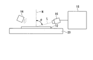
- FIG. 1 is a schematic configuration diagram showing an example of an anodized alumina inspection apparatus according to the present invention.
- the inspection apparatus includes a rotating means (not shown) for rotating a roll-shaped mold 12 in which anodized alumina having two or more pores is formed on the surface of a roll-shaped aluminum substrate, and a line shape on the mold 12.
- a linear illumination device 14 (illuminating means) that irradiates light
- a color line CCD camera 16 imaging means
- images reflected light from the surface of the anodized alumina of the mold 12 and an image from the color line CCD camera 16
- an image processing device 18 image processing means for processing signals.
- the line illumination device 14 is arranged so that the longitudinal direction of the light irradiation range to the mold 12 is orthogonal to the circumferential direction (rotation direction) of the mold 12.
- Examples of the line illumination device 14 include a fluorescent lamp lighting device for high-frequency lighting, rod illumination, optical fiber illumination arranged in a line, LED illumination, and the like. Further, the illumination may be a planar illumination device or a spot illumination device regardless of the line illumination device.
- the color line CCD camera 16 is a camera in which two or more color CCD elements are arranged one-dimensionally, and the color CCD illuminates the light irradiated from the line illumination device 14 and reflected from the surface of the anodized alumina of the mold 12. Light is received by the element, and RGB image signals are output for each pixel.
- the color line CCD camera 16 is arranged so that the longitudinal direction of the imaging range is orthogonal to the circumferential direction (rotation direction) of the mold 12. Further, the color line CCD camera 16 has an angle ⁇ of the optical axis L of the color line CCD camera 16 of 45 to 89.degree. With respect to the normal N of the surface (tangent plane) of the anodized alumina of the mold 12 in the imaging range. It is preferable to arrange it at 9 °. When the angle ⁇ is 45 ° or more, the color of the reflected light on the surface of the anodized alumina corresponding to the pore aspect ratio (depth / pitch) of the anodized alumina clearly appears.
- the angle ⁇ is 65 ° or more, it is less susceptible to noise than when it is 45 °.
- the angle ⁇ is more preferably 80 ° or more, and the angle ⁇ is more preferably 85 ° or more. If the angle ⁇ exceeds 89.9 °, imaging becomes difficult.
- the angle ⁇ is preferably 45 ° to 89.9 °, more preferably 65 ° to 89.9 °, still more preferably 80 ° to 89.9 °, and particularly preferably 85 ° to 89.9 °.
- the image processing device 18 acquires 256-tone RGB image signals for each pixel output from the color line CCD camera 16, and based on the acquired image signals, the aspect ratio (depth) of the pores of the anodized alumina. / Pitch) is determined to be within a predetermined range.
- the RGB image signal is converted into the HSV color system, and the aspect ratio (depth) of the pores of the anodized alumina is converted based on the digital information of the gradation (H). It is also possible to determine whether (the pitch / pitch) is within a predetermined range.
- the predetermined range of the aspect ratio (depth / pitch) can be arbitrarily set, is preferably 0.5 to 4.0, more preferably 1.0 to 3.5, and 1.8 to 3 .5 is more preferable, and 2.0 to 3.0 is most preferable.
- NG pixels whose color gradation is outside the preset gradation range are extracted, and the ratio of NG pixels in a predetermined region (for example, 2000 ⁇ 4000 pixels) is a predetermined ratio.
- a predetermined region for example, 2000 ⁇ 4000 pixels
- the ratio of NG pixels in a predetermined region is a predetermined ratio.
- the determination is performed using RGB image signals
- the determination is performed as follows.
- the depth of pores and the pitch between pores of the anodized alumina of the mold 12 are designed to be 200 nm and 100 nm (aspect ratio: 2), respectively, and the designed anodized alumina is formed, the anodized alumina
- R: 190, G: 160, and B: 120 are obtained. Therefore, the color range in the non-defective mold 12 is set to be within ⁇ 10 for any one of RGB, for example.
- the HSV color system is determined, for example, the following is performed.
- the depth of pores and the pitch between pores of the anodized alumina of the mold 12 are designed to be 200 nm and 100 nm (aspect ratio: 2), respectively, and the designed anodized alumina is formed, the anodized alumina
- the pore depth and pitch between the pores of the anodized alumina of the mold 12 are designed to be 100 nm and 100 nm (aspect ratio: 1), respectively.
- the depth of the pores and the pitch between the pores of the anodized alumina of the mold 12 are designed to be 200 nm and 200 nm (aspect ratio: 1), respectively, and the designed anodized alumina is formed
- the means for performing HSV conversion and determination may be realized by dedicated hardware, and the means for performing HSV conversion and determination is constituted by at least a memory and a central processing unit (CPU).
- the function may be realized by loading a program for realizing the replacement and determination functions into a memory and executing the program.
- an input device, a display device, and the like are connected to the image processing apparatus as peripheral devices.
- the input device refers to an input device such as a display touch panel, a switch panel, and a keyboard
- the display device refers to a CRT, a liquid crystal display device, and the like.
- the surface of the roll-shaped aluminum substrate is anodized under conditions such that the pore depth of the anodized alumina and the pitch between the pores are 200 nm and 100 nm (aspect ratio: 2), respectively. Get 12.
- the mold 12 is attached to the rotating means, and light is irradiated from the line illumination device 14 onto the surface of the anodized alumina of the rotating roll-shaped mold 12.
- the reflected light from the surface of the anodized alumina is imaged by the color line CCD camera 16.
- the image processing device 18 converts the RGB image signal for each pixel to the HSV color system as necessary. Conversion is performed to obtain digital information of a color (hue (H)) expressed in 256 gradations.
- an NG in which the tone of the hue (H) is out of a preset tone range (for example, H 14 to 34) from the image of one turn on the surface of the anodized alumina of the mold 12.
- a pixel is extracted and the ratio of NG pixels in a predetermined area (for example, 2000 ⁇ 4000 pixels) exceeds a predetermined ratio (for example, 5%), it is determined that the mold 12 to be inspected is defective. .
- the color of the reflected light on the surface of the anodized alumina depends on the aspect ratio (depth / pitch) of the pores of the anodized alumina. It is possible to estimate whether the aspect ratio of the pores of the anodized alumina is formed as designed by utilizing the change, for example, the depth of the pores by observing the cross section of the anodized alumina using an electron microscope. Compared to the method of measuring the pitch between the pores, it is possible to easily inspect whether the pore depth of the anodized alumina and the pitch between the pores are formed as designed.
- the anodized alumina inspection apparatus of the present invention includes an illumination unit that irradiates light on the surface of the anodized alumina, an imaging unit that images reflected light from the surface of the anodized alumina, and an image captured by the imaging unit. And image processing means for determining whether the aspect ratio (depth / pitch) of the pores of the anodized alumina is within a predetermined range based on the color information obtained from FIG.
- the examples are not limited.
- an inspection apparatus that inspects a plate-shaped mold 12 that moves in the horizontal direction by the moving means 20 may be used.
- a method for determining that the mold 12 to be inspected is a defective product is not limited to the above-described method.
- the color line CCD camera is used in the above-described imaging means, it may be an inspection device that measures a reflection spectrum with a photodetector and determines a non-defective product and a defective product from the reflection spectrum.
- a processing method of the image signal in the image processing apparatus it is processed as an image signal of 256 gradations. However, since it is sufficient that the normal part and the abnormal part can be discriminated from the image signal, Alternatively, an analog signal may be used.
- First oxide film forming step (a) The surface of the mirror-finished aluminum substrate is anodized in an electrolytic solution under a constant voltage to form an oxide film on the surface (hereinafter also referred to as step (a)).
- Second oxide film forming step (c) The aluminum base material on which the pore generation point is formed is anodized again in the electrolytic solution under a constant voltage, and an oxide film having pores corresponding to the pore generation point is formed on the surface (hereinafter, step (c) ).)
- Hole diameter expansion processing step (d) The diameter of the pores is enlarged (hereinafter also referred to as step (d)).
- step (e) If necessary, the second oxide film forming step (c) and the pore diameter expansion treatment step (d) are repeated (hereinafter also referred to as step (e)).
- tapered pores whose diameter gradually decreases in the depth direction from the opening are periodically formed on the surface of the mirror-finished aluminum base material.
- a mold having an anodized alumina having two or more pores formed on the surface can be obtained.
- a pretreatment for removing the oxide film on the surface of the aluminum substrate may be performed before the step (a).
- the method for removing the oxide film include a method of dipping in a chromic acid / phosphoric acid mixed solution.
- the step (a) may be performed instead of the step (a) depending on the use of the material to which the mold surface is transferred.
- each process will be described in detail.
- the electrolytic solution include an acidic electrolytic solution and an alkaline electrolytic solution, and an acidic electrolytic solution is preferable.
- the acidic electrolyte include oxalic acid, sulfuric acid, and a mixture thereof.
- the concentration of oxalic acid is preferably 0.7 M or less. If the concentration of oxalic acid exceeds 0.7M, the current value during anodic oxidation becomes too high, and the surface of the oxide film may become rough. Further, by setting the voltage during anodization to 30 to 60 V, it is possible to obtain a mold having anodized alumina having highly regular pores with a pitch of about 100 nm formed on the surface. Regardless of whether the voltage during anodization is higher or lower than this range, the regularity tends to decrease, and the pitch may be larger than the wavelength of visible light.
- the temperature of the electrolytic solution is preferably 60 ° C.
- the concentration of sulfuric acid is preferably 0.7 M or less. If the concentration of sulfuric acid exceeds 0.7M, the current value at the time of anodization may become too high to maintain a constant voltage. Further, by setting the voltage during anodization to 25 to 30 V, it is possible to obtain a mold on the surface of which anodized alumina having highly regular pores with a pitch of about 63 nm is formed. Regardless of whether the voltage during anodization is higher or lower than this range, the regularity tends to decrease, and the pitch may be larger than the wavelength of visible light.
- the temperature of the electrolytic solution is preferably 30 ° C. or less, and more preferably 20 ° C. or less. When the temperature of the electrolytic solution exceeds 30 ° C., a phenomenon called “burning” tends to occur, and the pores may be broken or the surface may melt and the regularity of the pores may be disturbed.
- the oxide film formed by anodizing for a long time becomes thick and the regularity of the arrangement of the pores can be improved.
- the thickness of the oxide film is 30 ⁇ m or less. By doing so, the macro unevenness
- the thickness of the oxide film is more preferably 1 to 10 ⁇ m, and further preferably 1 to 3 ⁇ m. The thickness of the oxide film can be observed with a field emission scanning electron microscope or the like.
- the regularity of the finally formed pores can be improved (for example, Masuda, “Applied Physics”). ", 2000, 69, No. 5, p. 558.). If the pores do not need to have high regularity, the oxide film 32 may be completely removed in step (b), or at least part of it may be removed.
- Examples of the method of removing the oxide film 32 include a method of removing aluminum with a solution that selectively dissolves alumina without dissolving aluminum.
- Examples of such a solution include a chromic acid / phosphoric acid mixed solution.
- anodic oxidation may be performed under the same conditions (electrolyte concentration, electrolyte temperature, formation voltage, etc.) as in step (a). Thereby, as shown in FIG. 3, the oxide film 35 in which the columnar pores 34 are formed can be formed. Even in the step (c), deeper pores can be obtained as the anodic oxidation is performed for a longer time.
- An oxide film having a thickness of about 0.01 to 0.5 ⁇ m may be formed, and it is not necessary to form an oxide film as thick as that formed in step (a).
- a pore diameter expansion treatment a method of immersing in a solution dissolving alumina and expanding the diameter of the pores formed in the step (c) by etching can be mentioned. Examples of such a solution include a phosphoric acid aqueous solution of about 5% by mass. The longer the time of step (d), the larger the pore diameter.
- step (c) is performed again, and the shape of the pores 34 is changed to a two-stage columnar shape with different diameters, as shown in FIG. 3, and then step (d) is performed again.
- the shape of the pores 34 is gradually tapered from the opening in the depth direction as shown in FIG.
- Various conditions of pores can be formed by appropriately setting the conditions of step (c) and step (d), for example, the time of anodization and the time of pore diameter expansion treatment. Therefore, these conditions may be set as appropriate according to the use of the article to be manufactured from the mold.
- this mold is for manufacturing an antireflection article such as an antireflection film
- the pitch and depth of the pores can be arbitrarily changed by appropriately setting the conditions in this way, so that it is optimal. It is also possible to design a refractive index change.
- the mold thus produced has a fine concavo-convex structure on the surface as a result of the formation of a large number of periodic pores.
- the pitch of the pores in this fine concavo-convex structure is not more than the wavelength of visible light, that is, not more than 400 nm, a so-called moth-eye structure is obtained.
- the pitch is a distance from the center of the concave portion (pore) of the fine concavo-convex structure to the center of the concave portion (pore) adjacent thereto.
- the pitch is larger than 400 nm, visible light scattering occurs, so that a sufficient antireflection function is not exhibited, and it is not suitable for manufacturing an antireflection article such as an antireflection film.
- the pitch is preferably 50 nm to 400 nm, more preferably 70 nm to 300 nm, and still more preferably 80 nm to 250 nm.
- the pitch of the pores is not more than the wavelength of visible light
- the depth of the pores is preferably 50 nm or more, and 100 nm. More preferably.
- the depth is a distance from the opening of the concave portion (pore) of the fine concavo-convex structure to the deepest portion. If the depth of the pores is 50 nm or more, the reflectance of the surface of the article for optical use formed by the transfer of the mold surface, that is, the transfer surface is lowered.
- the aspect ratio (depth / pitch) of the mold pores is preferably 1.0 to 4.0, more preferably 1.3 to 3.5, still more preferably 1.8 to 3.5. Most preferred is 0 to 3.0.
- the aspect ratio is 1.0 or more, a transfer surface with low reflectance can be formed, and the incident angle dependency and wavelength dependency thereof are sufficiently reduced. If the aspect ratio is greater than 4.0, the mechanical strength of the transfer surface tends to decrease.
- the shape of the mold may be a flat plate or a roll.
- the surface on which the fine uneven structure of the mold is formed may be subjected to a release treatment so that the release is easy.
- the release treatment method include a method of coating a silicone-based polymer or a fluorine polymer, a method of depositing a fluorine compound, a method of coating a fluorine-based or fluorine-silicone-based silane coupling agent, and the like.
- the mold manufactured as described above is a flat plate
- the reflected light from the surface of the anodized alumina is converted into a color line CCD by the inspection apparatus shown in FIG.
- An image is taken by the camera 16.
- the image processing device 18 converts the RGB image signal for each pixel into the HSV color system as necessary, and outputs the color ( Hue (H)) information is obtained.
- the quality of the mold 12 is judged from the acquired color information, and if it is a good product, the mold 12 is advanced to the manufacturing process of an article having a fine concavo-convex structure on the surface. If it is a defective product and is a uniform defect throughout the mold, a defect having a deep or shallow nanohole pore depth overall, or a defect in which the pitch of the nanohole pores is generally wide or narrow, Any one of the anodizing steps (a) to (e) is performed again on the mold 12 to repair the anodized alumina.
- the anodized alumina layer is made of an aluminum base. The whole material may be removed and the anodizing steps (a) to (e) may be performed from the beginning. After re-forming the anodized alumina, the inspection is performed again, and the anodizing process and the inspection process are repeated until the mold 12 becomes a good product.
- Example 1 Using the inspection apparatus shown in FIG. 1, the mold was inspected for anodized alumina by the above-described inspection method.
- the mold 12 was a mold c.
- the line illumination device 14 a fluorescent light source FL20SS ⁇ EX-N / 18 manufactured by Panasonic was used at 40 kHz.
- the color line CCD camera 16 a CV-L107CL-3CCD manufactured by JAI was used.
- MIL9 manufactured by Matrox was used.
- the color line CCD camera 16 has an angle ⁇ of the optical axis L of the color line CCD camera 16 of 5 ° to 85 ° with respect to the normal N of the surface (tangent plane) of the anodized alumina of the mold 12 in the imaging range. Images were taken while changing the conditions. The distance between the mold 12 and the color line CCD camera 16 was about 50 cm.
- the line illumination device 14 is arranged so that the reflected light enters the color line CCD camera 16.
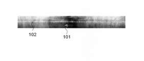
- An abnormal pore portion 101 of anodized alumina is imaged black in the vicinity of the center of the image.
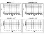
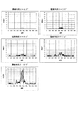
- An image picked up with an angle ⁇ of the optical axis L every 10 ° between 5 ° and 85 ° is converted from an RGB signal to a hue (H) signal by the image processing device 18 and one line of data including an abnormal portion.
- the hue (H) is normally expressed by 0 to 360 °, but 0 to 360 ° is expressed by 8 bit data of 0 to 255 in the image processing apparatus 18.
- the data position of one line is one line indicated by 102 in FIG. 4, and is the data at the same position in the image captured at the angle ⁇ of the other optical axis L.
- the vertical axis of each graph in FIG. 5 and FIG. 6 is a value obtained by taking a difference from the hue (H) of the abnormal part with the hue (H) of the normal part as a reference.
- the horizontal axis is a pixel.
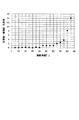
- FIG. 7 shows a plot of the hue difference between the normal part and the abnormal part in each captured image at intervals of 5 ° between the imaging angles of 5 ° to 85 °.
- the form for carrying out the present invention is that the angle ⁇ of the optical axis L of the color line CCD camera with respect to the normal N of the surface (tangent plane) of the anodized alumina of the mold in the imaging range. Is possible from 45 ° or more, preferably 65 ° or more, more preferably 80 ° or more, and further preferably 85 ° or more.
- Example 2 Using the inspection apparatus shown in FIG. 1, the mold was inspected for anodized alumina by the above-described inspection method. The mold 12 was a mold d.
- the line illumination device 14 a fluorescent light source FL20SS ⁇ EX-N / 18 manufactured by Panasonic was used at 40 kHz.
- the color line CCD camera 16 a CV-L107CL-3CCD manufactured by JAI was used.
- MIL9 manufactured by Matrox was used.
- the angle ⁇ of the optical axis L of the color line CCD camera 16 is 80 ° with respect to the normal N of the surface (tangent plane) of the anodized alumina of the mold 12 in the imaging range.
- the distance between the mold 12 and the color line CCD camera 16 was about 50 cm.
- the line illumination device 14 is arranged so that the reflected light enters the color line CCD camera 16.
- An image obtained by imaging one surface of the anodized alumina surface of the mold 12 was converted from an RGB signal into an 8-bit data hue (H) signal of 0 to 255 by the image processing device 18.
- the hue signal for one round of the surface of the anodized alumina was averaged over the entire image, and pixels different from the average value by 1.0 or more were determined as abnormal portions, but no abnormal portion was detected in the mold 12.
- a transparent film having a fine concavo-convex structure on the surface was produced using the mold 12, a film without unevenness could be produced.
- the transparent film which similarly has the fine concavo-convex structure on the surface was produced with the mold c used in Example 2 as reference, it became a film with unevenness.
- the step of inspecting the pore shape of the anodized alumina according to the present invention can easily inspect the pore depth of the anodized alumina and the pitch between the pores, and the shape of the pore is stable.
- Anodized alumina can be produced.
- Anodized alumina production method, inspection method, and inspection apparatus include an anodized alumina having two or more pores whose pitch is equal to or less than the wavelength of visible light by anodizing the surface of an aluminum substrate. This is useful for producing a mold formed on the surface.
Landscapes
- Chemical & Material Sciences (AREA)
- Engineering & Computer Science (AREA)
- Physics & Mathematics (AREA)
- General Physics & Mathematics (AREA)
- Metallurgy (AREA)
- Chemical Kinetics & Catalysis (AREA)
- Organic Chemistry (AREA)
- Materials Engineering (AREA)
- Electrochemistry (AREA)
- Pathology (AREA)
- Biochemistry (AREA)
- Analytical Chemistry (AREA)
- Health & Medical Sciences (AREA)
- General Health & Medical Sciences (AREA)
- Life Sciences & Earth Sciences (AREA)
- Immunology (AREA)
- Computer Vision & Pattern Recognition (AREA)
- General Chemical & Material Sciences (AREA)
- Mathematical Physics (AREA)
- Dispersion Chemistry (AREA)
- Automation & Control Theory (AREA)
- Investigating Materials By The Use Of Optical Means Adapted For Particular Applications (AREA)
- Investigating Or Analysing Materials By Optical Means (AREA)
- Length Measuring Devices By Optical Means (AREA)
- Spectrometry And Color Measurement (AREA)
Abstract
Description
本願は2010年3月25日に日本に出願された特願2010-070279号に基づき優先権を主張し、その内容をここに援用する。
(i)透明基材等の表面を直接加工して微細凹凸構造を表面に有する物品を製造する方法。
(ii)微細凹凸構造に対応した反転構造を有するモールドを用いて、透明基材等の表面に反転構造を転写する方法。
アルミニウム基材の表面を陽極酸化することによって形成される陽極酸化アルミナは、アルミニウムの酸化皮膜(アルマイト)であり、ピッチが可視光の波長以下である2個以上の細孔からなる微細凹凸構造を有する。
陽極酸化アルミナからの反射光の色は、しゃぼんだまに見られるような一般的な薄膜の干渉色だけではなく、陽極酸化アルミナの細孔の深さやピッチなどの構造の影響を反映したものである。
(1)2個以上の細孔を有する陽極酸化アルミナを製造する方法であって、陽極酸化アルミナ形成後に陽極酸化アルミナ表面に照明手段から光を照射すること、前記陽極酸化アルミナの表面からの反射光を撮像手段にて撮像すること、前記撮像手段により撮像された画像から色の情報を取得すること、および前記色の情報に基づいて、前記陽極酸化アルミナの細孔の形状を検査することを含む陽極酸化アルミナの製造方法。
(2)前記陽極酸化アルミナの表面からの反射光を撮像手段にて撮像することが、前記陽極酸化アルミナ表面の法線に対して、前記撮像手段の光軸の角度が45~89.9°となるように撮像することを含む、(1)に記載の陽極酸化アルミナの製造方法。
(3)前記陽極酸化アルミナの表面からの反射光を撮像手段にて撮像することが、前記陽極酸化アルミナ表面の法線に対して、前記撮像手段の光軸の角度が65~89.9°となるように撮像することを含む、(1)に記載の陽極酸化アルミナの製造方法。
(4)前記陽極酸化アルミナの表面からの反射光を撮像手段にて撮像することが、前記陽極酸化アルミナ表面の法線に対して、前記撮像手段の光軸の角度が80~89.9°となるように撮像することを含む、(1)に記載の陽極酸化アルミナの製造方法。
(5)前記色の情報に基づいて陽極酸化アルミナの細孔の形状を検査することが、前記陽極酸化アルミナの表面からの反射光をRGB信号として撮像すること、および前記RGB信号の情報に基づいて前記陽極酸化アルミナの細孔の形状を検査することを含む、(1)に記載の陽極酸化アルミナの製造方法。
(6)前記色の情報に基づいて陽極酸化アルミナの細孔の形状を検査することが、前記陽極酸化アルミナの表面からの反射光をRGB信号として撮像すること、前記RGB信号をHSV表色系に変換すること、および前記HSV表色系の情報に基づいて前記陽極酸化アルミナの細孔の形状を検査することを含む、(1)に記載の陽極酸化アルミナの製造方法。
(7)前記陽極酸化アルミナ形成後に陽極酸化アルミナ表面に照明手段から光を照射することの前に、さらに、下記の工程(a)~(e)を含む前記陽極酸化アルミナを形成する工程を有する、(1)に記載の陽極酸化アルミナの製造方法。
(a)鏡面化されたアルミニウム基材の表面を電解液中、定電圧下で陽極酸化して、表面に酸化皮膜を形成する工程。
(b)前記酸化皮膜を除去し、陽極酸化の細孔発生点を前記アルミニウム基材の表面に形成する工程。
(c)前記細孔発生点が形成されたアルミニウム基材の表面を、電解液中、定電圧下で再度陽極酸化して、前記細孔発生点に対応した細孔を有する酸化皮膜を表面に形成する工程。
(d)前記細孔の径を拡大させる工程。
(e)前記工程(c)と工程(d)とを繰り返し行う工程。
(9)前記陽極酸化アルミナの表面からの反射光を撮像手段にて撮像することが、前記陽極酸化アルミナ表面の法線に対して、前記撮像手段の光軸の角度が45~89.9°となるように撮像することを含む、(8)に記載の陽極酸化アルミナの検査方法。
(10)前記陽極酸化アルミナの表面からの反射光を撮像手段にて撮像することが、前記陽極酸化アルミナ表面の法線に対して、前記撮像手段の光軸の角度が65~89.9°となるように撮像することを含む、(8)に記載の陽極酸化アルミナの検査方法。
(11)前記陽極酸化アルミナの表面からの反射光を撮像手段にて撮像することが、前記陽極酸化アルミナ表面の法線に対して、前記撮像手段の光軸の角度が80~89.9°となるように撮像することを含む、(8)に記載の陽極酸化アルミナの検査方法。
(12)前記色の情報に基づいて陽極酸化アルミナの細孔のアスペクト比(深さ/ピッチ)が所定の範囲内にあるかを判定することが、前記陽極酸化アルミナの表面からの反射光をRGB信号として撮像すること、および前記RGB信号の情報に基づいて前記陽極酸化アルミナの細孔の形状を検査することを含む、(8)に記載の陽極酸化アルミナの検査方法。
(13)前記色の情報に基づいて陽極酸化アルミナの細孔のアスペクト比(深さ/ピッチ)が所定の範囲内にあるかを判定することが、前記陽極酸化アルミナの表面からの反射光をRGB信号として撮像すること、前記RGB信号をHSV表色系に変換すること、および前記HSV表色系の情報に基づいて前記陽極酸化アルミナの細孔の形状を検査することを含む、(8)に記載の陽極酸化アルミナの検査方法。
(15)前記陽極酸化アルミナの表面からの反射光を撮像する撮像手段が、前記陽極酸化アルミナ表面の法線に対して、前記撮像手段の光軸の角度が45~89.9°となるように撮像する手段である、(14)に記載の陽極酸化アルミナの検査装置。
(16)前記陽極酸化アルミナの表面からの反射光を撮像する撮像手段が、前記陽極酸化アルミナ表面の法線に対して、前記撮像手段の光軸の角度が65~89.9°となるように撮像する手段である、(14)に記載の陽極酸化アルミナの検査装置。
(17)前記陽極酸化アルミナの表面からの反射光を撮像する撮像手段が、前記陽極酸化アルミナ表面の法線に対して、前記撮像手段の光軸の角度が80~89.9°となるように撮像する手段である、(14)に記載の陽極酸化アルミナの検査装置。
(18)前記色の情報に基づいて陽極酸化アルミナの細孔のアスペクト比(深さ/ピッチ)が所定の範囲内にあるかを判定する画像処理手段が、前記陽極酸化アルミナの表面からの反射光をRGB信号として撮像する手段と、前記RGB信号の情報に基づいて前記陽極酸化アルミナの細孔の形状を検査する手段とを含む、(14)に記載の陽極酸化アルミナの検査装置。
(19)前記色の情報に基づいて陽極酸化アルミナの細孔のアスペクト比(深さ/ピッチ)が所定の範囲内にあるかを判定する画像処理手段が、前記陽極酸化アルミナの表面からの反射光をRGB信号として撮像する手段と、前記RGB信号をHSV表色系に変換する手段と、前記HSV表色系の情報に基づいて前記陽極酸化アルミナの細孔の形状を検査する手段とを含む、(14)に記載の陽極酸化アルミナの検査装置。
図1は、本発明の陽極酸化アルミナの検査装置の一例を示す概略構成図である。
検査装置は、2個以上の細孔を有する陽極酸化アルミナがロール状のアルミニウム基材の表面に形成された、ロール状のモールド12を回転させる回転手段(図示略)と、モールド12にライン状に光を照射するライン状照明装置14(照明手段)と、モールド12の陽極酸化アルミナの表面からの反射光を撮像するカラーラインCCDカメラ16(撮像手段)と、カラーラインCCDカメラ16からの画像信号を処理する画像処理装置18(画像処理手段)とを有する。
ライン状照明装置14としては、高周波点灯の蛍光灯点灯装置、ロッド照明、ライン状に配置された光ファイバ照明、およびLED照明等が挙げられる。
また、照明はライン状照明装置に関わらず、面状照明装置、またはスポット状照明装置でもよい。
前記角度θは45°~89.9°が好ましく、65°~89.9°がより好ましく、80°~89.9°がさらに好ましく、85°~89.9°が特に好ましい。
また、判定の簡単化の目的で、RGBの画像信号をHSV表色系に変換し、階調化された色相(H)のデジタル情報に基づいて、陽極酸化アルミナの細孔のアスペクト比(深さ/ピッチ)が所定の範囲内にあるかを判定することも可能である。
前記アスペクト比(深さ/ピッチ)の所定の範囲とは、任意に設定することができ、0.5~4.0が好ましく、1.0~3.5がより好ましく、1.8~3.5がさらに好ましく、2.0~3.0が最も好ましい。
モールド12の陽極酸化アルミナの細孔の深さおよび細孔間のピッチを、それぞれ200nmおよび100nm(アスペクト比:2)と設計し、設計どおりの陽極酸化アルミナが形成された場合、前記陽極酸化アルミナの反射光の色を実測すると、R:190、G:160、B:120となる。よって、良品のモールド12における色の範囲は、例えばRGBのいずれか一つでも±10以内と設定する。
モールド12の陽極酸化アルミナの細孔の深さおよび細孔間のピッチを、それぞれ200nmおよび100nm(アスペクト比:2)と設計し、設計どおりの陽極酸化アルミナが形成された場合、前記陽極酸化アルミナの反射光の色相(H)を実測すると、薄い赤(H=24前後)となる。よって、良品のモールド12における色相(H)の階調の範囲は、例えば14~34と設定する。
また、画像処理装置には、周辺機器として、入力装置、表示装置等が接続されるものとする。ここで、入力装置とは、ディスプレイタッチパネル、スイッチパネル、およびキーボード等の入力デバイスのことをいい、表示装置とは、CRT、および液晶表示装置等のことをいう。
図1に示す検査装置を用いた陽極酸化アルミナの検査方法について説明する。
陽極酸化アルミナの表面からの反射光をカラーラインCCDカメラ16にて撮像する。
また、検査対象のモールド12が不良品であると判定する方法も、上述の方法に限定されない。
また、撮像手段も上述ではカラーラインCCDカメラを用いているが、光検出器にて反射スペクトルを測定し、反射スペクトルから良品、および不良品を判定する検査装置であってもよい。
また、画像処理装置における画像信号の処理方法として、256階調の画像信号として処理しているが、画像信号から正常部と異常部を判別できれば良いため、512階調でも、1024階調でも、もしくはアナログ信号であってもよい。
以下、アルミニウム基材の表面を陽極酸化することによって、ピッチが可視光の波長以下である2個以上の細孔を有する陽極酸化アルミナが表面に形成されたモールドについて説明する。
第1の酸化皮膜形成工程(a):
鏡面化されたアルミニウム基材の表面を電解液中、定電圧下で陽極酸化して、表面に酸化皮膜を形成する(以下、工程(a)とも記す。)。
酸化皮膜除去工程(b):
酸化皮膜の少なくとも一部を除去し、陽極酸化の細孔発生点を形成する(以下、工程(b)とも記す。)。
第2の酸化皮膜形成工程(c):
細孔発生点が形成されたアルミニウム基材を電解液中、定電圧下で再度陽極酸化して、細孔発生点に対応した細孔を有する酸化皮膜を表面に形成する(以下、工程(c)とも記す。)。
孔径拡大処理工程(d):
細孔の径を拡大させる(以下、工程(d)とも記す。)。
繰り返し工程(e):
必要に応じて、第2の酸化皮膜形成工程(c)と孔径拡大処理工程(d)とを繰り返し行う(以下、工程(e)とも記す。)。
また、細孔の配列の規則性はやや低下するが、モールドの表面を転写した材料の用途によっては工程(a)を行わず、工程(c)から行ってもよい。
以下、各工程を詳細に説明する。
第1の酸化皮膜形成工程(a)では、鏡面化されたアルミニウム基材の表面を電解液中、定電圧下で陽極酸化し、図3に示すように、アルミニウム基材30の表面に、細孔31を有する酸化皮膜32を形成する。
電解液としては、酸性電解液、およびアルカリ性電解液が挙げられ、酸性電解液が好ましい。
酸性電解液としては、シュウ酸、硫酸、およびこれらの混合物等が挙げられる。
また、陽極酸化時の電圧を30~60Vとすることにより、ピッチが100nm程度の規則性の高い細孔を有する陽極酸化アルミナが表面に形成されたモールドを得ることができる。陽極酸化時の電圧がこの範囲より高くても低くても規則性が低下する傾向にあり、ピッチが可視光の波長より大きくなることがある。
電解液の温度は、60℃以下が好ましく、45℃以下がより好ましい。電解液の温度が60℃を超えると、いわゆる「ヤケ」といわれる現象が起こる傾向にあり、細孔が壊れたり、表面が溶けて細孔の規則性が乱れたりすることがある。
また、陽極酸化時の電圧を25~30Vとすることにより、ピッチが63nm程度の規則性の高い細孔を有する陽極酸化アルミナが表面に形成されたモールドを得ることができる。陽極酸化時の電圧がこの範囲より高くても低くても規則性が低下する傾向があり、ピッチが可視光の波長より大きくなることがある。
電解液の温度は、30℃以下が好ましく、20℃以下がより好ましい。電解液の温度が30℃を超えると、いわゆる「ヤケ」といわれる現象が起こる傾向にあり、細孔が壊れたり、表面が溶けて細孔の規則性が乱れたりすることがある。
工程(a)の後、工程(a)により形成された酸化皮膜32を除去することにより、図3に示すように、除去された酸化皮膜32の底部(バリア層と呼ばれる)に対応する周期的な窪み、すなわち、細孔発生点33を形成することができる。
形成された酸化皮膜32を一旦除去し、陽極酸化の細孔発生点33を形成することで、最終的に形成される細孔の規則性を向上させることができる(例えば、益田、「応用物理」、2000年、第69巻、第5号、p.558参照。)。なお、細孔が高い規則性を有する必要がない場合、工程(b)において酸化被膜32を完全に除去しても良く、少なくとも一部を除去するようにしても構わない。
細孔発生点33が形成されたアルミニウム基材30を電解液中、定電圧下で再度陽極酸化し、再び酸化皮膜を形成する。
工程(c)では、工程(a)と同様の条件(電解液濃度、電解液温度、および化成電圧等)下で陽極酸化すればよい。
これにより、図3に示すように、円柱状の細孔34が形成された酸化皮膜35を形成できる。工程(c)においても、陽極酸化を長時間施すほど、深い細孔を得ることができるが、例えば反射防止物品などの光学用の物品を製造するためのモールドを製造する場合には、ここでは0.01~0.5μm程度の酸化皮膜を形成すればよく、工程(a)で形成するほどの厚さの酸化皮膜を形成する必要はない。
工程(c)の後、工程(c)で形成された細孔34の径を拡大させる孔径拡大処理を行って、図3に示すように、細孔34の径を拡径する。
孔径拡大処理の具体的方法としては、アルミナを溶解する溶液に浸漬して、工程(c)で形成された細孔の径をエッチングにより拡大させる方法が挙げられる。このような溶液としては、例えば、5質量%程度のリン酸水溶液等が挙げられる。工程(d)の時間を長くするほど、細孔の径は大きくなる。
再度、工程(c)を行って、図3に示すように、細孔34の形状を径の異なる2段の円柱状とし、その後、再度、工程(d)を行う。このように工程(c)と工程(d)を繰り返す、繰り返し工程(e)により、図3に示すように、細孔34の形状を開口部から深さ方向に徐々に径が縮小するテーパ形状にでき、その結果、周期的な2個以上の細孔を有する陽極酸化アルミナが表面に形成されたモールド12を得ることができる。
ピッチは、微細凹凸構造の凹部(細孔)の中心からこれに隣接する凹部(細孔)の中心までの距離である。
ピッチが400nmより大きいと可視光の散乱が起こるため、十分な反射防止機能は発現せず、反射防止膜等の反射防止物品の製造には適さない。
前記ピッチは、50nm以上400nm以下が好ましく、70nm以上300nm以下がより好ましく、80nm以上250nm以下がさらに好ましい。
深さは、微細凹凸構造の凹部(細孔)の開口部から最深部までの距離である。
細孔の深さが50nm以上であれば、モールドの表面の転写により形成された光学用途の物品の表面、すなわち転写面の反射率が低下する。
モールドの微細凹凸構造が形成された表面は、離型が容易になるように、離型処理が施されていてもよい。離型処理の方法としては、例えば、シリコーン系ポリマーやフッ素ポリマーをコーティングする方法、フッ素化合物を蒸着する方法、およびフッ素系またはフッ素シリコーン系のシランカップリング剤をコーティングする方法等が挙げられる。
直径:65mm、厚さ:2mmの円板状のアルミニウム基材(純度99.99%)を、算術平均粗さRaが20nm以下となる条件にて鏡面研磨した。
工程(a):
前記アルミニウム基材について、0.3Mシュウ酸水溶液中で、直流:40V、温度:16℃の条件で30分間陽極酸化を行った。
工程(b):
酸化皮膜が形成されたアルミニウム基材を、6質量%リン酸/1.8質量%クロム酸混合水溶液に浸漬して、酸化皮膜を除去した。
前記アルミニウム基材について、0.3Mシュウ酸水溶液中で、直流:40V、温度:16℃の条件で30秒間陽極酸化を行った。
工程(d):
酸化皮膜が形成されたアルミニウム基材を、30℃の5質量%リン酸水溶液に8分間浸漬して、細孔径拡大処理を行った。
工程(e):
前記工程(c)および工程(d)を合計で5回繰り返し、平均ピッチ:100nm、深さ:200nmの略円錐形状の細孔を有する陽極酸化アルミナが表面に形成された円板状のモールドaを得た。
前記工程(c)における陽極酸化の時間を20秒に変更した以外は、モールドaの製造と同様にして、平均ピッチ:100nm、深さ:100nmの略円錐形状の細孔を有する陽極酸化アルミナが表面に形成された円板状のモールドbを得た。
純度99.99%のアルミニウムインゴットを外径:200mm、内径:155mm、長さ:350mmに切断した圧延痕のない円筒状のアルミニウム基材に、羽布研磨処理を施した後、これを過塩素酸/エタノール混合溶液中(体積比:1/4)で電解研磨し、鏡面化した。
前記アルミニウム基材について、0.3Mシュウ酸水溶液中で、直流:40V、温度:16℃の条件で30分間陽極酸化を行った。
工程(b):
厚さ3μmの酸化皮膜が形成されたアルミニウム基材を、6質量%リン酸/1.8質量%クロム酸混合水溶液に浸漬して、酸化皮膜を除去した。
前記アルミニウム基材について、0.3Mシュウ酸水溶液中で、直流:40V、温度:16℃の条件で30秒間陽極酸化を行った。この際、シュウ酸水溶液中の温度にムラが生じるように、シュウ酸水溶液の撹拌を止めた。
工程(d):
酸化皮膜が形成されたアルミニウム基材を、30℃の5質量%リン酸水溶液に8分間浸漬して、細孔径拡大処理を行った。
工程(e):
前記工程(c)および工程(d)を合計で5回繰り返し、設計上では平均ピッチ:100nm、深さ:200nmの略円錐形状の細孔を有する陽極酸化アルミナが表面に形成されたロール状のモールドcを得た。
前記工程(c)におけるシュウ酸水溶液中の温度にムラが生じないように、シュウ酸水溶液の撹拌を実施した以外は、モールドcの製造と同様にして、平均ピッチ:100nm、深さ:200nmの略円錐形状の細孔を有する陽極酸化アルミナが表面に形成されたロール状のモールドdを得た。
陽極酸化アルミナが形成された面が上側となるように、モールドaを卓上に設置し、約30cm離れた場所から、デジタルカメラ(キヤノン社製、IXY DIGITAL 55)にて陽極酸化アルミナの表面を撮影した。この際、モールドaの陽極酸化アルミナの表面(接平面)の法線Nに対して、デジタルカメラの光軸Lの角度θが約70°となるように撮影した。
撮影の結果、平均ピッチ:100nm、深さ:200nm(アスペクト比:2)の略円錐形状の細孔を有する陽極酸化アルミナの表面は、薄い赤色であることが確認された。
モールドaをモールドbに変更した以外は、参考例1と同様にして陽極酸化アルミナの表面を撮影した。
撮影の結果、平均ピッチ:100nm、深さ:100nm(アスペクト比:1)の略円錐形状の細孔を有する陽極酸化アルミナの表面は、薄い緑色であることが確認された。
図1に示す検査装置を用い、上述の検査方法にてモールドの陽極酸化アルミナの検査を実施した。
モールド12は、モールドcとした。
ライン状照明装置14としては、Panasonic社製の蛍光光源FL20SS・EX-N/18を40kHzにて用いた。
カラーラインCCDカメラ16としては、JAI社製のCV-L107CL-3CCDを用いた。
画像処理装置18としては、Matrox社製のMIL9を用いた。
モールド12とカラーラインCCDカメラ16との距離は約50cmとした。
ライン状照明装置14は反射光がカラーラインCCDカメラ16に入るように配置した。
陽極酸化アルミナの細孔異常部101が画像中央付近に黒く撮像されている。
色相(H)は通常、0~360°で表現するが、画像処理装置18内では0~360°を0~255の8bitデータで表現している。
1ラインのデータ位置は、図4の102で示す1ラインであり、他の光軸Lの角度θで撮像した画像においても同じ位置のデータである。
図5および図6の各グラフの縦軸は正常部の色相(H)を基準とし、異常部との色相(H)との差分を取った値である。また、横軸は画素である。
撮像角度5°~85°間の5°おきの各撮像画像にて正常部と異常部の色相差をプロットしたものを図7に示した。
光軸Lの角度θ=65°では45°の時よりも正常部と異常部の色相差が大きいため感度良く検出でき、光軸Lの角度θ=80°ではさらに検出感度が高くなり、図7の光軸Lの角度θ=85°ではさらに感度良く検出できる。
〔実施例2〕
図1に示す検査装置を用い、上述の検査方法にてモールドの陽極酸化アルミナの検査を実施した。
モールド12は、モールドdとした。
ライン状照明装置14としては、Panasonic社製の蛍光光源FL20SS・EX-N/18を40kHzにて用いた。
カラーラインCCDカメラ16としては、JAI社製のCV-L107CL-3CCDを用いた。
画像処理装置18としては、Matrox社製のMIL9を用いた。
モールド12とカラーラインCCDカメラ16との距離は約50cmとした。
ライン状照明装置14は反射光がカラーラインCCDカメラ16に入るように配置した。
陽極酸化アルミナの表面1周分の色相信号を画像全体に渡って平均し、その平均値から1.0以上異なる画素を異常部としたが、モールド12において異常部は検出されなかった。
モールド12を用いて、微細凹凸構造を表面に有する透明フィルムを作製した所、ムラの無いフィルムを作ることができた。
また、参考として実施例2にて用いたモールドcにて同様に微細凹凸構造を表面に有する透明フィルムを作製した所、ムラの有るフィルムとなった。
14 ライン状照明装置(照明手段)
16 カラーラインCCDカメラ(撮像手段)
18 画像処理装置(画像処理手段)
34 細孔
35 酸化皮膜(陽極酸化アルミナ)
101 陽極酸化アルミナの細孔異常部
Claims (19)
- 2個以上の細孔を有する陽極酸化アルミナを製造する方法であって、
陽極酸化アルミナ形成後に陽極酸化アルミナ表面に照明手段から光を照射すること、
前記陽極酸化アルミナの表面からの反射光を撮像手段にて撮像すること、
前記撮像手段により撮像された画像から色の情報を取得すること、および
前記色の情報に基づいて、前記陽極酸化アルミナの細孔の形状を検査することを含む陽極酸化アルミナの製造方法。 - 前記陽極酸化アルミナの表面からの反射光を撮像手段にて撮像することが、
前記陽極酸化アルミナ表面の法線に対して、前記撮像手段の光軸の角度が45~89.9°となるように撮像することを含む、請求項1に記載の陽極酸化アルミナの製造方法。 - 前記陽極酸化アルミナの表面からの反射光を撮像手段にて撮像することが、
前記陽極酸化アルミナ表面の法線に対して、前記撮像手段の光軸の角度が65~89.9°となるように撮像することを含む、請求項1に記載の陽極酸化アルミナの製造方法。 - 前記陽極酸化アルミナの表面からの反射光を撮像手段にて撮像することが、
前記陽極酸化アルミナ表面の法線に対して、前記撮像手段の光軸の角度が80~89.9°となるように撮像することを含む、請求項1に記載の陽極酸化アルミナの製造方法。 - 前記色の情報に基づいて陽極酸化アルミナの細孔の形状を検査することが、
前記陽極酸化アルミナの表面からの反射光をRGB信号として撮像すること、および
前記RGB信号の情報に基づいて前記陽極酸化アルミナの細孔の形状を検査することを含む、請求項1に記載の陽極酸化アルミナの製造方法。 - 前記色の情報に基づいて陽極酸化アルミナの細孔の形状を検査することが、
前記陽極酸化アルミナの表面からの反射光をRGB信号として撮像すること、
前記RGB信号をHSV表色系に変換すること、および
前記HSV表色系の情報に基づいて前記陽極酸化アルミナの細孔の形状を検査することを含む、請求項1に記載の陽極酸化アルミナの製造方法。 - 前記陽極酸化アルミナ形成後に陽極酸化アルミナ表面に照明手段から光を照射することの前に、さらに、下記の工程(a)~(e)を含む前記陽極酸化アルミナを形成する工程を有する、請求項1に記載の陽極酸化アルミナの製造方法。
(a)鏡面化されたアルミニウム基材の表面を電解液中、定電圧下で陽極酸化して、表面に酸化皮膜を形成する工程。
(b)前記酸化皮膜を除去し、陽極酸化の細孔発生点を前記アルミニウム基材の表面に形成する工程。
(c)前記細孔発生点が形成されたアルミニウム基材の表面を、電解液中、定電圧下で再度陽極酸化して、前記細孔発生点に対応した細孔を有する酸化皮膜を表面に形成する工程。
(d)前記細孔の径を拡大させる工程。
(e)前記工程(c)と工程(d)とを繰り返し行う工程。 - 2個以上の細孔を有する陽極酸化アルミナを検査する方法であって、
前記陽極酸化アルミナの表面に照明手段から光を照射すること、
前記陽極酸化アルミナの表面からの反射光を撮像手段にて撮像すること、
前記撮像手段により撮像された画像から色の情報を取得すること、および
前記色の情報に基づいて、前記陽極酸化アルミナの細孔のアスペクト比(深さ/ピッチ)が所定の範囲内にあるかを判定することを含む、陽極酸化アルミナの検査方法。 - 前記陽極酸化アルミナの表面からの反射光を撮像手段にて撮像することが、
前記陽極酸化アルミナ表面の法線に対して、前記撮像手段の光軸の角度が45~89.9°となるように撮像することを含む、請求項8に記載の陽極酸化アルミナの検査方法。 - 前記陽極酸化アルミナの表面からの反射光を撮像手段にて撮像することが、
前記陽極酸化アルミナ表面の法線に対して、前記撮像手段の光軸の角度が65~89.9°となるように撮像することを含む、請求項8に記載の陽極酸化アルミナの検査方法。 - 前記陽極酸化アルミナの表面からの反射光を撮像手段にて撮像することが、
前記陽極酸化アルミナ表面の法線に対して、前記撮像手段の光軸の角度が80~89.9°となるように撮像することを含む、請求項8に記載の陽極酸化アルミナの検査方法。 - 前記色の情報に基づいて陽極酸化アルミナの細孔のアスペクト比(深さ/ピッチ)が所定の範囲内にあるかを判定することが、
前記陽極酸化アルミナの表面からの反射光をRGB信号として撮像すること、および
前記RGB信号の情報に基づいて前記陽極酸化アルミナの細孔の形状を検査することを含む、請求項8に記載の陽極酸化アルミナの検査方法。 - 前記色の情報に基づいて陽極酸化アルミナの細孔のアスペクト比(深さ/ピッチ)が所定の範囲内にあるかを判定することが、
前記陽極酸化アルミナの表面からの反射光をRGB信号として撮像すること、
前記RGB信号をHSV表色系に変換すること、および
前記HSV表色系の情報に基づいて前記陽極酸化アルミナの細孔の形状を検査することを含む、請求項8に記載の陽極酸化アルミナの検査方法。 - 2個以上の細孔を有する陽極酸化アルミナを検査する装置であって、
前記陽極酸化アルミナの表面に光を照射する照明手段と、
前記陽極酸化アルミナの表面からの反射光を撮像する撮像手段と、
前記撮像手段により撮像された画像から得られた色の情報に基づいて、前記陽極酸化アルミナの細孔のアスペクト比(深さ/ピッチ)が所定の範囲内にあるかを判定する画像処理手段と
を有する、陽極酸化アルミナの検査装置。 - 前記陽極酸化アルミナの表面からの反射光を撮像する撮像手段が、
前記陽極酸化アルミナ表面の法線に対して、前記撮像手段の光軸の角度が45~89.9°となるように撮像する手段である、請求項14に記載の陽極酸化アルミナの検査装置。 - 前記陽極酸化アルミナの表面からの反射光を撮像する撮像手段が、
前記陽極酸化アルミナ表面の法線に対して、前記撮像手段の光軸の角度が65~89.9°となるように撮像する手段である、請求項14に記載の陽極酸化アルミナの検査装置。 - 前記陽極酸化アルミナの表面からの反射光を撮像する撮像手段が、
前記陽極酸化アルミナ表面の法線に対して、前記撮像手段の光軸の角度が80~89.9°となるように撮像する手段である、請求項14に記載の陽極酸化アルミナの検査装置。 - 前記色の情報に基づいて陽極酸化アルミナの細孔のアスペクト比(深さ/ピッチ)が所定の範囲内にあるかを判定する画像処理手段が、
前記陽極酸化アルミナの表面からの反射光をRGB信号として撮像する手段と、
前記RGB信号の情報に基づいて前記陽極酸化アルミナの細孔の形状を検査する手段とを含む、請求項14に記載の陽極酸化アルミナの検査装置。 - 前記色の情報に基づいて陽極酸化アルミナの細孔のアスペクト比(深さ/ピッチ)が所定の範囲内にあるかを判定する画像処理手段が、
前記陽極酸化アルミナの表面からの反射光をRGB信号として撮像する手段と、
前記RGB信号をHSV表色系に変換する手段と、
前記HSV表色系の情報に基づいて前記陽極酸化アルミナの細孔の形状を検査する手段とを含む、請求項14に記載の陽極酸化アルミナの検査装置。
Priority Applications (4)
| Application Number | Priority Date | Filing Date | Title |
|---|---|---|---|
| CN201180015235.2A CN102844473B (zh) | 2010-03-25 | 2011-03-22 | 阳极氧化铝的制造方法、检查装置以及检查方法 |
| KR1020127025354A KR101345049B1 (ko) | 2010-03-25 | 2011-03-22 | 양극 산화 알루미나의 제조 방법, 검사 장치 및 검사 방법 |
| JP2011514981A JP5049405B2 (ja) | 2010-03-25 | 2011-03-22 | 陽極酸化アルミナの製造方法、検査装置および検査方法 |
| US13/637,251 US8780350B2 (en) | 2010-03-25 | 2012-09-25 | Method for manufacturing anodized alumina, and device and method for inspecting the same |
Applications Claiming Priority (2)
| Application Number | Priority Date | Filing Date | Title |
|---|---|---|---|
| JP2010-070279 | 2010-03-25 | ||
| JP2010070279 | 2010-03-25 |
Related Child Applications (1)
| Application Number | Title | Priority Date | Filing Date |
|---|---|---|---|
| US13/637,251 Continuation-In-Part US8780350B2 (en) | 2010-03-25 | 2012-09-25 | Method for manufacturing anodized alumina, and device and method for inspecting the same |
Publications (1)
| Publication Number | Publication Date |
|---|---|
| WO2011118596A1 true WO2011118596A1 (ja) | 2011-09-29 |
Family
ID=44673147
Family Applications (1)
| Application Number | Title | Priority Date | Filing Date |
|---|---|---|---|
| PCT/JP2011/056865 Ceased WO2011118596A1 (ja) | 2010-03-25 | 2011-03-22 | 陽極酸化アルミナの製造方法、検査装置および検査方法 |
Country Status (6)
| Country | Link |
|---|---|
| US (1) | US8780350B2 (ja) |
| JP (1) | JP5049405B2 (ja) |
| KR (1) | KR101345049B1 (ja) |
| CN (1) | CN102844473B (ja) |
| TW (1) | TWI408257B (ja) |
| WO (1) | WO2011118596A1 (ja) |
Cited By (7)
| Publication number | Priority date | Publication date | Assignee | Title |
|---|---|---|---|---|
| WO2013047593A1 (ja) * | 2011-09-26 | 2013-04-04 | 三菱レイヨン株式会社 | 微細凹凸構造を表面に有する部材の検査装置および検査方法、陽極酸化アルミナ層を表面に有する部材の製造方法、及び光学フィルムの製造方法 |
| JP2013112892A (ja) * | 2011-12-01 | 2013-06-10 | Dnp Fine Chemicals Co Ltd | ナノ構造体作製用型体の製造方法、製造装置、ナノ構造体作製用型体及びナノ構造体 |
| JP2013135136A (ja) * | 2011-12-27 | 2013-07-08 | Horon:Kk | 円筒状原版検査装置および円筒状原版検査方法 |
| JPWO2013008643A1 (ja) * | 2011-07-08 | 2015-02-23 | シャープ株式会社 | 形状検査方法、構造物の製造方法及び形状検査装置 |
| JP2018128436A (ja) * | 2017-02-10 | 2018-08-16 | 株式会社パパラボ | 表面粗さ判定装置及び判定方法 |
| US20200300745A1 (en) * | 2019-03-22 | 2020-09-24 | Ngk Insulators, Ltd. | Method for estimating characteristics of ceramic fired body |
| JP2022123932A (ja) * | 2021-02-15 | 2022-08-25 | プライムプラネットエナジー&ソリューションズ株式会社 | ナノ突起構造体検査装置およびナノ突起構造体検査方法 |
Families Citing this family (7)
| Publication number | Priority date | Publication date | Assignee | Title |
|---|---|---|---|---|
| FI20135688L (fi) * | 2013-06-24 | 2014-12-25 | Outotec Finland Oy | Menetelmä ja järjestely metallien elektrolyyttistä raffinointia varten valettujen anodien valmistamiseksi elektrolyyttistä raffinointivaihetta varten |
| JP6354384B2 (ja) * | 2014-06-27 | 2018-07-11 | 三菱ケミカル株式会社 | モールドの検査方法およびモールドの製造方法 |
| JP6423011B2 (ja) * | 2015-01-23 | 2018-11-14 | 株式会社日立ハイテクノロジーズ | パターン測定装置及び欠陥検査装置 |
| CN106645196B (zh) * | 2016-12-15 | 2020-08-11 | 广东威创视讯科技股份有限公司 | 投影镜头的灰尘检测装置及灰尘清除装置 |
| CN114504723A (zh) * | 2021-12-22 | 2022-05-17 | 融冲(深圳)生物医疗科技有限责任公司 | 聚合物球囊及其制备方法 |
| CN115976587B (zh) * | 2023-02-21 | 2023-08-22 | 中国地质大学(北京) | 电解着色表面氧化层低反射率的生产工艺及系统 |
| CN118408947B (zh) * | 2024-07-02 | 2024-11-01 | 南通楚捷电子设备有限公司 | 应用于金属表面阳极氧化后的检测方法 |
Citations (3)
| Publication number | Priority date | Publication date | Assignee | Title |
|---|---|---|---|---|
| JPH06294634A (ja) * | 1993-04-12 | 1994-10-21 | Kobe Steel Ltd | 感光体ドラムの表面形状測定評価方法 |
| JP2001205327A (ja) * | 2000-01-28 | 2001-07-31 | Sumitomo Metal Ind Ltd | 表面性状判別装置 |
| JP2006284569A (ja) * | 2005-03-10 | 2006-10-19 | Fuji Photo Film Co Ltd | 基材処理装置及び基材処理方法 |
Family Cites Families (6)
| Publication number | Priority date | Publication date | Assignee | Title |
|---|---|---|---|---|
| JPH09101265A (ja) * | 1995-10-05 | 1997-04-15 | Furukawa Electric Co Ltd:The | Al板の表面欠陥自動検査法 |
| JP3932812B2 (ja) * | 2001-02-20 | 2007-06-20 | 住友金属鉱山株式会社 | 帯状金属処理面の検査装置 |
| US7597936B2 (en) * | 2002-11-26 | 2009-10-06 | University Of Utah Research Foundation | Method of producing a pigmented composite microporous material |
| JP4406553B2 (ja) | 2003-11-21 | 2010-01-27 | 財団法人神奈川科学技術アカデミー | 反射防止膜の製造方法 |
| EP1580305A3 (en) * | 2004-03-23 | 2008-01-16 | FUJIFILM Corporation | Fine structural body surface and method of producing the same |
| JP5286938B2 (ja) * | 2008-05-27 | 2013-09-11 | 東京エレクトロン株式会社 | 針跡検査装置、プローブ装置、及び針跡検査方法、並びに記憶媒体 |
-
2011
- 2011-03-22 JP JP2011514981A patent/JP5049405B2/ja not_active Expired - Fee Related
- 2011-03-22 CN CN201180015235.2A patent/CN102844473B/zh not_active Expired - Fee Related
- 2011-03-22 WO PCT/JP2011/056865 patent/WO2011118596A1/ja not_active Ceased
- 2011-03-22 KR KR1020127025354A patent/KR101345049B1/ko not_active Expired - Fee Related
- 2011-03-23 TW TW100109887A patent/TWI408257B/zh active
-
2012
- 2012-09-25 US US13/637,251 patent/US8780350B2/en active Active
Patent Citations (3)
| Publication number | Priority date | Publication date | Assignee | Title |
|---|---|---|---|---|
| JPH06294634A (ja) * | 1993-04-12 | 1994-10-21 | Kobe Steel Ltd | 感光体ドラムの表面形状測定評価方法 |
| JP2001205327A (ja) * | 2000-01-28 | 2001-07-31 | Sumitomo Metal Ind Ltd | 表面性状判別装置 |
| JP2006284569A (ja) * | 2005-03-10 | 2006-10-19 | Fuji Photo Film Co Ltd | 基材処理装置及び基材処理方法 |
Cited By (10)
| Publication number | Priority date | Publication date | Assignee | Title |
|---|---|---|---|---|
| JPWO2013008643A1 (ja) * | 2011-07-08 | 2015-02-23 | シャープ株式会社 | 形状検査方法、構造物の製造方法及び形状検査装置 |
| WO2013047593A1 (ja) * | 2011-09-26 | 2013-04-04 | 三菱レイヨン株式会社 | 微細凹凸構造を表面に有する部材の検査装置および検査方法、陽極酸化アルミナ層を表面に有する部材の製造方法、及び光学フィルムの製造方法 |
| JP2013112892A (ja) * | 2011-12-01 | 2013-06-10 | Dnp Fine Chemicals Co Ltd | ナノ構造体作製用型体の製造方法、製造装置、ナノ構造体作製用型体及びナノ構造体 |
| JP2013135136A (ja) * | 2011-12-27 | 2013-07-08 | Horon:Kk | 円筒状原版検査装置および円筒状原版検査方法 |
| JP2018128436A (ja) * | 2017-02-10 | 2018-08-16 | 株式会社パパラボ | 表面粗さ判定装置及び判定方法 |
| US20200300745A1 (en) * | 2019-03-22 | 2020-09-24 | Ngk Insulators, Ltd. | Method for estimating characteristics of ceramic fired body |
| JP2020153954A (ja) * | 2019-03-22 | 2020-09-24 | 日本碍子株式会社 | セラミックス焼成体の特性推定方法 |
| US11614394B2 (en) * | 2019-03-22 | 2023-03-28 | Ngk Insulators, Ltd. | Method for estimating characteristics of ceramic fired body |
| JP2022123932A (ja) * | 2021-02-15 | 2022-08-25 | プライムプラネットエナジー&ソリューションズ株式会社 | ナノ突起構造体検査装置およびナノ突起構造体検査方法 |
| JP7191137B2 (ja) | 2021-02-15 | 2022-12-16 | プライムプラネットエナジー&ソリューションズ株式会社 | ナノ突起構造体検査装置およびナノ突起構造体検査方法 |
Also Published As
| Publication number | Publication date |
|---|---|
| CN102844473B (zh) | 2014-04-16 |
| TWI408257B (zh) | 2013-09-11 |
| TW201134986A (en) | 2011-10-16 |
| KR20120135416A (ko) | 2012-12-13 |
| JPWO2011118596A1 (ja) | 2013-07-04 |
| KR101345049B1 (ko) | 2013-12-26 |
| JP5049405B2 (ja) | 2012-10-17 |
| US20130206601A1 (en) | 2013-08-15 |
| US8780350B2 (en) | 2014-07-15 |
| CN102844473A (zh) | 2012-12-26 |
Similar Documents
| Publication | Publication Date | Title |
|---|---|---|
| JP5049405B2 (ja) | 陽極酸化アルミナの製造方法、検査装置および検査方法 | |
| JP5449570B2 (ja) | 微細凹凸構造を表面に有する部材の検査装置および検査方法、陽極酸化アルミナ層を表面に有する部材の製造方法、及び光学フィルムの製造方法 | |
| JP2012255652A (ja) | 陽極酸化アルミナの検査装置および検査方法、ならびに陽極酸化アルミナを表面に有する部材の製造方法 | |
| US10338005B2 (en) | Apparatus for inspecting back surface of epitaxial wafer and method of inspecting back surface of epitaxial wafer using the same | |
| RU2431161C1 (ru) | Антиотражающая пленка, оптический элемент, содержащий антиотражающую пленку, штамп, способ изготовления штампа и способ производства антиотражающей пленки | |
| TWI443228B (zh) | 模具及模具之製造方法與抗反射膜之製造方法 | |
| JP6354384B2 (ja) | モールドの検査方法およびモールドの製造方法 | |
| US20200072762A1 (en) | Method of inspecting back surface of epitaxial wafer, epitaxial wafer back surface inspection apparatus, method of managing lift pin of epitaxial growth apparatus, and method of producing epitaxial wafer | |
| TWI457589B (zh) | 蛾眼用模與蛾眼用模及蛾眼構造之製作方法 | |
| JPWO2011052652A1 (ja) | 型および型の製造方法ならびに反射防止膜 | |
| JP5059985B2 (ja) | 型の検査方法 | |
| JP2011220810A (ja) | 金属の欠陥検出方法及び欠陥検出装置 | |
| JP2015129706A (ja) | 微細凹凸構造を表面に有する物品の検査装置および検査方法、並びに微細凹凸構造を表面に有する物品の製造方法 | |
| US10695955B2 (en) | Mold manufacturing method and anti-reflective film manufacturing method | |
| JP5673088B2 (ja) | 微細凹凸構造を表面に有する物品の製造方法および製造装置 | |
| JP2014206449A (ja) | 鏡面切削した部材の検査装置および検査方法、鏡面切削した部材の製造方法、ならびに光学フィルムの製造方法 | |
| JP2010008066A (ja) | Vaパターン欠損検査方法および検査装置 | |
| CN118243015B (zh) | 表面三维形貌的测量方法、装置、设备、介质和程序产品 | |
| JP5899638B2 (ja) | 反射防止フィルム製造用金型の製造方法 | |
| KR20250028949A (ko) | 웨이퍼 및 그 형상 분석 방법 |
Legal Events
| Date | Code | Title | Description |
|---|---|---|---|
| WWE | Wipo information: entry into national phase |
Ref document number: 201180015235.2 Country of ref document: CN |
|
| WWE | Wipo information: entry into national phase |
Ref document number: 2011514981 Country of ref document: JP |
|
| 121 | Ep: the epo has been informed by wipo that ep was designated in this application |
Ref document number: 11759401 Country of ref document: EP Kind code of ref document: A1 |
|
| NENP | Non-entry into the national phase |
Ref country code: DE |
|
| ENP | Entry into the national phase |
Ref document number: 20127025354 Country of ref document: KR Kind code of ref document: A |
|
| 122 | Ep: pct application non-entry in european phase |
Ref document number: 11759401 Country of ref document: EP Kind code of ref document: A1 |