WO2011111578A1 - 高周波結合器 - Google Patents
高周波結合器 Download PDFInfo
- Publication number
- WO2011111578A1 WO2011111578A1 PCT/JP2011/054735 JP2011054735W WO2011111578A1 WO 2011111578 A1 WO2011111578 A1 WO 2011111578A1 JP 2011054735 W JP2011054735 W JP 2011054735W WO 2011111578 A1 WO2011111578 A1 WO 2011111578A1
- Authority
- WO
- WIPO (PCT)
- Prior art keywords
- antenna element
- path
- circuit board
- circle
- frequency coupler
- Prior art date
- Legal status (The legal status is an assumption and is not a legal conclusion. Google has not performed a legal analysis and makes no representation as to the accuracy of the status listed.)
- Ceased
Links
Images



Classifications
-
- H—ELECTRICITY
- H04—ELECTRIC COMMUNICATION TECHNIQUE
- H04B—TRANSMISSION
- H04B5/00—Near-field transmission systems, e.g. inductive or capacitive transmission systems
- H04B5/20—Near-field transmission systems, e.g. inductive or capacitive transmission systems characterised by the transmission technique; characterised by the transmission medium
- H04B5/24—Inductive coupling
- H04B5/26—Inductive coupling using coils
-
- H—ELECTRICITY
- H01—ELECTRIC ELEMENTS
- H01Q—ANTENNAS, i.e. RADIO AERIALS
- H01Q7/00—Loop antennas with a substantially uniform current distribution around the loop and having a directional radiation pattern in a plane perpendicular to the plane of the loop
-
- G—PHYSICS
- G06—COMPUTING OR CALCULATING; COUNTING
- G06K—GRAPHICAL DATA READING; PRESENTATION OF DATA; RECORD CARRIERS; HANDLING RECORD CARRIERS
- G06K19/00—Record carriers for use with machines and with at least a part designed to carry digital markings
- G06K19/06—Record carriers for use with machines and with at least a part designed to carry digital markings characterised by the kind of the digital marking, e.g. shape, nature, code
- G06K19/067—Record carriers with conductive marks, printed circuits or semiconductor circuit elements, e.g. credit or identity cards also with resonating or responding marks without active components
- G06K19/07—Record carriers with conductive marks, printed circuits or semiconductor circuit elements, e.g. credit or identity cards also with resonating or responding marks without active components with integrated circuit chips
- G06K19/077—Constructional details, e.g. mounting of circuits in the carrier
-
- H—ELECTRICITY
- H01—ELECTRIC ELEMENTS
- H01Q—ANTENNAS, i.e. RADIO AERIALS
- H01Q1/00—Details of, or arrangements associated with, antennas
- H01Q1/36—Structural form of radiating elements, e.g. cone, spiral, umbrella; Particular materials used therewith
- H01Q1/38—Structural form of radiating elements, e.g. cone, spiral, umbrella; Particular materials used therewith formed by a conductive layer on an insulating support
-
- H—ELECTRICITY
- H01—ELECTRIC ELEMENTS
- H01Q—ANTENNAS, i.e. RADIO AERIALS
- H01Q21/00—Antenna arrays or systems
- H01Q21/06—Arrays of individually energised antenna units similarly polarised and spaced apart
Definitions
- the present invention relates to a high-frequency coupler used for high-frequency signal communication.
- This proximity wireless transfer technology is a technology for performing contactless communication via an antenna using an induction electric field.
- This proximity wireless transfer technology is a technology capable of transferring a large amount of data at a high speed in a short time, and is suitable for transferring a large amount of data such as music data or moving image data.
- this proximity wireless transfer technology is assumed to have a communication distance of several centimeters or less, and has an advantage that the possibility of data leakage during communication is low.
- Patent Document 1 a high-frequency coupler having a structure in which a coupling electrode is formed of a linear conductor and folded in a coil shape has been proposed.
- Patent Document 2 a structure in which a high frequency coupler is formed on a substrate has been proposed.
- This high frequency coupler is assumed to be mounted on a small device such as a mobile phone, and there is a strong demand for downsizing and thinning.
- the high frequency coupler is to increase the tolerance of lateral deviation between the high frequency coupler on the transmission side and the high frequency coupler on the reception side. It is assumed that when the two high-frequency couplers on the transmission side and the reception side are correctly opposed to each other, sufficient coupling strength is obtained and communication between them is possible. Even in this case, it becomes difficult to use if the coupling strength sharply decreases when these two high-frequency couplers are shifted relatively sideways.
- the high frequency coupler disclosed in Patent Document 2 is formed on a substrate and is superior in terms of miniaturization as compared with the high frequency coupler disclosed in Patent Document 1, but as shown in a comparative example described later. It is considered that the tolerance for lateral displacement is lowered.
- An object of the present invention is to provide a high-frequency coupler that is more resistant to lateral shift while being reduced in size and thickness.
- the high-frequency coupler of the present invention that achieves the above object is formed on a surface of a circuit board and either the surface or the inner surface of the circuit board, and when the circle is drawn on the surface, An antenna element having a shape that circulates along the circle while alternately repeating a first path extending from the inside to the outside and a second path extending from the outside to the inside of the circle is provided.
- the first path and the second path that constitute the antenna element are both linearly extending paths, and the first path and the second path that are adjacent to each other are mutually connected. They may be alternately repeated in contact with each other with an angle between them.
- the high frequency coupler of the present invention has a second antenna element that circulates around the antenna element, which is formed on the surface or the inner surface of the circuit board.
- the high-frequency coupler of the present invention may have a loop antenna element that circulates around the antenna element on the surface of the circuit board.
- the transmitting high-frequency coupler and the receiving high-frequency coupler having the same antenna element are overlapped with each other and shifted laterally. According to the present invention, even when shifted laterally in this way, a pair of line segments that are close to each other in parallel are formed for transmission and reception, and thus strong coupling strength even if there is lateral displacement Is preserved.
- FIG. 1 is a view showing a front surface (A) and a back surface (B) of a high-frequency coupler according to an embodiment of the present invention.
- the high-frequency coupler 10 includes a circuit board 20, a star-shaped antenna element 30 formed on the surface of the circuit board 20, and a star shape on the surface of the circuit board 20.
- a loop antenna element 40 formed so as to circulate around the antenna element 30.
- a ground surface 33 is widely formed at the center of the back surface of the circuit board 20, and the star antenna element 30 is formed in the opening from which the ground surface 33 is cut.
- a power feeding section 34 is formed.
- One end of the star-shaped antenna element 30 formed on the surface of the circuit board 20 is connected to a power feeding portion 34 formed on the back surface of the circuit board 20 through a through hole 38.
- the other end of the star-shaped antenna element 30 is connected to the ground surface 33 on the back surface of the circuit board 20 through the through hole 39.
- two power feeding portions 41 for the loop antenna element 40 are formed on the back surface of the circuit board 20. Both ends of the loop antenna element 40 formed on the surface of the circuit board 20 are connected to the two power feeding portions 41 on the back surface of the circuit board 20 through the through holes 49, respectively.
- the star-shaped antenna element 30 includes a first path 31 extending from the inside of the circle 37 to the outside when the circle 37 is drawn on the surface of the circuit board 20 and a second path 32 extending from the outside of the circle 37 to the inside. And alternately and repeatedly around the circle 37.
- the first path 31 and the second path 32 are both linearly extending paths, and the first path 31 and the second path 32 adjacent to each other are mutually connected. It repeats alternately with an angle in between and touching each other.
- the loop antenna element 40 is formed on the surface of the circuit board 20 so as to circulate around the star-shaped antenna element 30 as described above. Both ends of the loop antenna element are connected to two power feeding portions 41 formed on the back surface of the circuit board 20 through a pair of through holes 49.
- the loop antenna element 40 is used as a so-called RFID radio antenna.
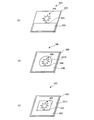
- FIG. 2 is a view showing a state (A) in which two circuit boards for transmission and reception are overlapped and a state (B) in which they are shifted laterally, each having an antenna element formed thereon.
- FIG. 3 is a diagram showing a state in which the circular antenna element is shifted laterally.
- This circular antenna element is a comparative antenna element compared with the embodiment of the present invention.
- the coupling strength between the transmitting antenna element and the receiving antenna element is roughly determined by the length of a pair of line segments that are close to each other and extend parallel to each other and the degree of proximity.
- the antenna element 50A for transmission and the antenna for reception are placed in the upper and lower parts of FIG. There are parallel line segment pairs close to each other with the element 50B. However, if they are greatly displaced as shown in FIG. 3B, the parallel parts are separated from each other, and only weak coupling strength is obtained.
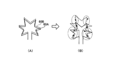
- FIG. 4 is a diagram showing a state in which the star-shaped antenna element is shifted laterally.
- FIG. 5 shows the relationship between the lateral shift amount and the coupling strength in the star-shaped antenna element (example) shown in FIG. 1 and the circular antenna element (comparative example) capable of transmitting and receiving in the same wavelength region.
- FIG. 5 shows the relationship between the lateral shift amount and the coupling strength in the star-shaped antenna element (example) shown in FIG. 1 and the circular antenna element (comparative example) capable of transmitting and receiving in the same wavelength region.
- Example is a star shape as shown in FIG. 1, has a width of about 10 mm, an antenna element whose length is determined so as to transmit and receive radio waves of 4 ⁇ 5GH Z bands. Furthermore, “comparative example” is a circular plate-shaped antenna elements, as in the “Examples", 4 ⁇ 5GH so long as to transmit and receive radio waves in the frequency band of Z are determined.
- the spacing in the facing direction between the transmitting antenna element and the receiving antenna element is 1 mm (see FIG. 2).
- the horizontal axis indicates the relative shift distance [mm]
- the vertical axis indicates the bond strength [dB].
- the coupling strength [dB] is expressed in decibels (dB) of the power transmitted to the receiving antenna element with respect to the power input to the transmitting antenna element.
- the bond strength is greatly reduced at a shift distance of about 10 mm or more, whereas in the case of the example, a sharp decrease in the bond strength as in the comparative example is seen. Absent. That is, in the case of the embodiment, even if the receiving antenna element is arranged at a position considerably deviated from the transmitting antenna element, communication is possible between them, and the practicality is excellent.
- FIG. 6 is a diagram showing various modifications of the embodiment shown in FIG.
- a high-frequency coupler 10A shown in FIG. 6A is an example in which a star-shaped antenna element 30A, a ground plane 33A, and a power feeding portion 34A are all formed on the same surface of the circuit board 20A.
- the high-frequency coupler of the present invention can also form all elements on only one surface of the circuit board.
- all elements of the star-shaped antenna element 30B, the ground surface 33B, and the power feeding portion 34B are formed on the same surface of the circuit board 20B as in FIG. 6A. This is an example. However, an opening 331B is formed in the ground surface 33B, and the antenna element 30B is disposed in the opening 331B.
- the star-shaped antenna element 30C, the ground surface 33C, and the feeding portion 34C are formed on the same surface of the circuit board 20C. is doing.
- the ground surface 33C extends so as to surround the antenna element 30C, as in FIG. 6B.
- the opening 331B surrounding the antenna element 30B has a partially circular arc shape
- the opening 331C surrounding the antenna element 30C is rectangular. .
- FIG. 1 and FIGS. 6A to 6C there can be various forms of arrangement of the antenna element and the ground plane.
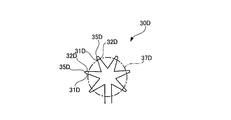
- FIG. 7 is a diagram showing a modification of the antenna element.
- the first path 31 and the second path 32 are formed in the circle 37 while being alternately in contact with each other at an angle between the inside and the outside of the circle 37. It is circling along.
- the first path 31D and the second path 32D are in direct contact with each other while forming an angle inside the circle 37D.
- the path 31D and the second path 32D are not in direct contact with each other.
- the first path 31D and the second path 32D are connected via a line segment 35D extending in parallel with the circle 37D.
- the first path 31D and the second path 32D may be connected via a curve instead of the line segment 35D.
- it may be connected via a line or curve, either inside the circle 37D, or both outside and inside the circle 37D.
- the first route and the second route are not necessarily directly connected as described above.
- the star-shaped antenna element is formed on the surface of the circuit board, but may be formed on the inner surface of the circuit board.
Landscapes
- Engineering & Computer Science (AREA)
- Computer Hardware Design (AREA)
- Microelectronics & Electronic Packaging (AREA)
- Physics & Mathematics (AREA)
- General Physics & Mathematics (AREA)
- Theoretical Computer Science (AREA)
- Computer Networks & Wireless Communication (AREA)
- Signal Processing (AREA)
- Details Of Aerials (AREA)
- Variable-Direction Aerials And Aerial Arrays (AREA)
- Near-Field Transmission Systems (AREA)
Abstract
Description
20,20A,20B,20C 回路基板
30,30A,30B,30C,30D,50A,50B,60A,60B アンテナ素子
31,31D 第1経路
32,32D 第2経路
33,33A,33B,33C グランド面
34,34A,34B,34C,41 給電部
35D 線分
37,37D 円
38,39,49 スルーホール
40 ループ状アンテナ素子
331B,331C 開口
Claims (3)
- 回路基板と、
前記回路基板の表面又は内面のうちのいずれかの面に形成された、該面上に円を描いたときの該円の内側から外側に延びる第1経路と、該円の外側から内側に延びる第2経路とを交互に繰り返しながら該円に沿って周回する形状のアンテナ素子とを備えたことを特徴とする高周波結合器。 - 前記第1経路および前記第2経路が、いずれも直線的に延びる経路であって、互いに隣接する第1経路と第2経路が互いの間に角を成し互いに接して交互に繰り返していることを特徴とする請求項1記載の高周波結合器。
- 前記回路基板の表面に、前記アンテナ素子を周回するループ状アンテナ素子を有することを特徴とする請求項1又は2記載の高周波結合器。
Priority Applications (2)
| Application Number | Priority Date | Filing Date | Title |
|---|---|---|---|
| KR1020127022413A KR20130006601A (ko) | 2010-03-11 | 2011-03-02 | 고주파 결합기 |
| CN201180013435.4A CN102782938B (zh) | 2010-03-11 | 2011-03-02 | 高频耦合器 |
Applications Claiming Priority (2)
| Application Number | Priority Date | Filing Date | Title |
|---|---|---|---|
| JP2010-054764 | 2010-03-11 | ||
| JP2010054764A JP5634084B2 (ja) | 2010-03-11 | 2010-03-11 | 高周波結合器 |
Publications (1)
| Publication Number | Publication Date |
|---|---|
| WO2011111578A1 true WO2011111578A1 (ja) | 2011-09-15 |
Family
ID=44563382
Family Applications (1)
| Application Number | Title | Priority Date | Filing Date |
|---|---|---|---|
| PCT/JP2011/054735 Ceased WO2011111578A1 (ja) | 2010-03-11 | 2011-03-02 | 高周波結合器 |
Country Status (5)
| Country | Link |
|---|---|
| JP (1) | JP5634084B2 (ja) |
| KR (1) | KR20130006601A (ja) |
| CN (1) | CN102782938B (ja) |
| TW (1) | TWM408891U (ja) |
| WO (1) | WO2011111578A1 (ja) |
Families Citing this family (3)
| Publication number | Priority date | Publication date | Assignee | Title |
|---|---|---|---|---|
| CN105098365B (zh) * | 2014-05-14 | 2018-08-10 | 3M创新有限公司 | 近场通信模块 |
| US10122192B2 (en) | 2015-02-17 | 2018-11-06 | Qualcomm Incorporated | Sense coil geometries with improved sensitivity for metallic object detection in a predetermined space |
| KR102261329B1 (ko) * | 2015-07-24 | 2021-06-04 | 엘지전자 주식회사 | 안테나, 차량용 레이더, 및 이를 구비하는 차량 |
Citations (2)
| Publication number | Priority date | Publication date | Assignee | Title |
|---|---|---|---|---|
| JP2006235824A (ja) * | 2005-02-23 | 2006-09-07 | Omron Corp | 広帯域icタグ |
| JP2007188252A (ja) * | 2006-01-12 | 2007-07-26 | Lintec Corp | アンテナ回路、icインレット、マルチタグ及びマルチタグ製造方法 |
Family Cites Families (3)
| Publication number | Priority date | Publication date | Assignee | Title |
|---|---|---|---|---|
| US6603440B2 (en) * | 2000-12-14 | 2003-08-05 | Protura Wireless, Inc. | Arrayed-segment loop antenna |
| EP2306586B1 (en) * | 2008-07-04 | 2014-04-02 | Murata Manufacturing Co. Ltd. | Wireless ic device |
| JP4650536B2 (ja) * | 2008-07-28 | 2011-03-16 | ソニー株式会社 | 電界結合器、通信装置、通信システム及び電界結合器の製造方法。 |
-
2010
- 2010-03-11 JP JP2010054764A patent/JP5634084B2/ja not_active Expired - Fee Related
-
2011
- 2011-01-31 TW TW100202220U patent/TWM408891U/zh not_active IP Right Cessation
- 2011-03-02 WO PCT/JP2011/054735 patent/WO2011111578A1/ja not_active Ceased
- 2011-03-02 KR KR1020127022413A patent/KR20130006601A/ko not_active Withdrawn
- 2011-03-02 CN CN201180013435.4A patent/CN102782938B/zh not_active Expired - Fee Related
Patent Citations (2)
| Publication number | Priority date | Publication date | Assignee | Title |
|---|---|---|---|---|
| JP2006235824A (ja) * | 2005-02-23 | 2006-09-07 | Omron Corp | 広帯域icタグ |
| JP2007188252A (ja) * | 2006-01-12 | 2007-07-26 | Lintec Corp | アンテナ回路、icインレット、マルチタグ及びマルチタグ製造方法 |
Also Published As
| Publication number | Publication date |
|---|---|
| JP2011188459A (ja) | 2011-09-22 |
| TWM408891U (en) | 2011-08-01 |
| KR20130006601A (ko) | 2013-01-17 |
| CN102782938A (zh) | 2012-11-14 |
| JP5634084B2 (ja) | 2014-12-03 |
| CN102782938B (zh) | 2015-12-16 |
Similar Documents
| Publication | Publication Date | Title |
|---|---|---|
| US9698460B2 (en) | Transmission of signals via a high-frequency waveguide | |
| KR101714537B1 (ko) | 미모 안테나 장치 | |
| US9100056B2 (en) | Waveguide structure for a contactless connector | |
| WO2010073421A1 (ja) | 携帯無線機 | |
| JP2012146237A (ja) | 信号伝送装置、電子機器、及び、信号伝送方法 | |
| US20110222585A1 (en) | High-frequency coupler and communication device | |
| JP2013009235A (ja) | 通信装置並びに通信システム | |
| WO2012111484A1 (ja) | 導波装置、通信モジュール、及び、電子機器 | |
| CN101938028B (zh) | 高频耦合器和通信装置 | |
| JP2015049717A (ja) | コネクタ、コネクタ組立体及び無線通信モジュール | |
| CN103384939B (zh) | 波导装置、通信模块、波导装置制造方法和电子设备 | |
| JP5634084B2 (ja) | 高周波結合器 | |
| KR20130098361A (ko) | 안테나 장치 및 통신 장치 | |
| US20140038516A1 (en) | Antenna structures for near field communications | |
| US20120306702A1 (en) | Substrate Antenna | |
| WO2011096416A1 (ja) | アンテナ装置、及び、通信装置 | |
| JP4311450B2 (ja) | アンテナ装置 | |
| JP6137355B2 (ja) | 信号伝送装置 | |
| KR20130140084A (ko) | 안테나 장치 및 통신 장치 | |
| JP5662889B2 (ja) | 無線モジュール | |
| JP6126494B2 (ja) | 基板型アンテナ | |
| JP2013214840A (ja) | 方向性結合器および無線通信装置 | |
| JP2012015848A (ja) | アンテナ装置、及び、通信装置 | |
| JP2014087050A (ja) | アンテナ構造及び当該アンテナ構造を備えた無線通信装置 |
Legal Events
| Date | Code | Title | Description |
|---|---|---|---|
| WWE | Wipo information: entry into national phase |
Ref document number: 201180013435.4 Country of ref document: CN |
|
| 121 | Ep: the epo has been informed by wipo that ep was designated in this application |
Ref document number: 11753237 Country of ref document: EP Kind code of ref document: A1 |
|
| ENP | Entry into the national phase |
Ref document number: 20127022413 Country of ref document: KR Kind code of ref document: A |
|
| NENP | Non-entry into the national phase |
Ref country code: DE |
|
| 122 | Ep: pct application non-entry in european phase |
Ref document number: 11753237 Country of ref document: EP Kind code of ref document: A1 |