WO2011108902A9 - Compound comprising at least two compounds comprising at least two five-membered hetero rings, an organic electrical element using the same and a terminal thereof - Google Patents
Compound comprising at least two compounds comprising at least two five-membered hetero rings, an organic electrical element using the same and a terminal thereof Download PDFInfo
- Publication number
- WO2011108902A9 WO2011108902A9 PCT/KR2011/001539 KR2011001539W WO2011108902A9 WO 2011108902 A9 WO2011108902 A9 WO 2011108902A9 KR 2011001539 W KR2011001539 W KR 2011001539W WO 2011108902 A9 WO2011108902 A9 WO 2011108902A9
- Authority
- WO
- WIPO (PCT)
- Prior art keywords
- substituted
- organic
- unsubstituted
- group
- carbon atoms
- Prior art date
Links
Images


Classifications
-
- H—ELECTRICITY
- H10—SEMICONDUCTOR DEVICES; ELECTRIC SOLID-STATE DEVICES NOT OTHERWISE PROVIDED FOR
- H10K—ORGANIC ELECTRIC SOLID-STATE DEVICES
- H10K85/00—Organic materials used in the body or electrodes of devices covered by this subclass
- H10K85/60—Organic compounds having low molecular weight
- H10K85/649—Aromatic compounds comprising a hetero atom
- H10K85/657—Polycyclic condensed heteroaromatic hydrocarbons
-
- C—CHEMISTRY; METALLURGY
- C07—ORGANIC CHEMISTRY
- C07D—HETEROCYCLIC COMPOUNDS
- C07D495/00—Heterocyclic compounds containing in the condensed system at least one hetero ring having sulfur atoms as the only ring hetero atoms
- C07D495/22—Heterocyclic compounds containing in the condensed system at least one hetero ring having sulfur atoms as the only ring hetero atoms in which the condensed system contains four or more hetero rings
-
- C—CHEMISTRY; METALLURGY
- C07—ORGANIC CHEMISTRY
- C07D—HETEROCYCLIC COMPOUNDS
- C07D519/00—Heterocyclic compounds containing more than one system of two or more relevant hetero rings condensed among themselves or condensed with a common carbocyclic ring system not provided for in groups C07D453/00 or C07D455/00
-
- C—CHEMISTRY; METALLURGY
- C09—DYES; PAINTS; POLISHES; NATURAL RESINS; ADHESIVES; COMPOSITIONS NOT OTHERWISE PROVIDED FOR; APPLICATIONS OF MATERIALS NOT OTHERWISE PROVIDED FOR
- C09B—ORGANIC DYES OR CLOSELY-RELATED COMPOUNDS FOR PRODUCING DYES, e.g. PIGMENTS; MORDANTS; LAKES
- C09B1/00—Dyes with anthracene nucleus not condensed with any other ring
-
- C—CHEMISTRY; METALLURGY
- C09—DYES; PAINTS; POLISHES; NATURAL RESINS; ADHESIVES; COMPOSITIONS NOT OTHERWISE PROVIDED FOR; APPLICATIONS OF MATERIALS NOT OTHERWISE PROVIDED FOR
- C09B—ORGANIC DYES OR CLOSELY-RELATED COMPOUNDS FOR PRODUCING DYES, e.g. PIGMENTS; MORDANTS; LAKES
- C09B57/00—Other synthetic dyes of known constitution
-
- H—ELECTRICITY
- H10—SEMICONDUCTOR DEVICES; ELECTRIC SOLID-STATE DEVICES NOT OTHERWISE PROVIDED FOR
- H10K—ORGANIC ELECTRIC SOLID-STATE DEVICES
- H10K85/00—Organic materials used in the body or electrodes of devices covered by this subclass
- H10K85/60—Organic compounds having low molecular weight
- H10K85/649—Aromatic compounds comprising a hetero atom
- H10K85/657—Polycyclic condensed heteroaromatic hydrocarbons
- H10K85/6572—Polycyclic condensed heteroaromatic hydrocarbons comprising only nitrogen in the heteroaromatic polycondensed ring system, e.g. phenanthroline or carbazole
-
- H—ELECTRICITY
- H10—SEMICONDUCTOR DEVICES; ELECTRIC SOLID-STATE DEVICES NOT OTHERWISE PROVIDED FOR
- H10K—ORGANIC ELECTRIC SOLID-STATE DEVICES
- H10K85/00—Organic materials used in the body or electrodes of devices covered by this subclass
- H10K85/60—Organic compounds having low molecular weight
- H10K85/649—Aromatic compounds comprising a hetero atom
- H10K85/657—Polycyclic condensed heteroaromatic hydrocarbons
- H10K85/6576—Polycyclic condensed heteroaromatic hydrocarbons comprising only sulfur in the heteroaromatic polycondensed ring system, e.g. benzothiophene
-
- H—ELECTRICITY
- H10—SEMICONDUCTOR DEVICES; ELECTRIC SOLID-STATE DEVICES NOT OTHERWISE PROVIDED FOR
- H10K—ORGANIC ELECTRIC SOLID-STATE DEVICES
- H10K2102/00—Constructional details relating to the organic devices covered by this subclass
-
- Y—GENERAL TAGGING OF NEW TECHNOLOGICAL DEVELOPMENTS; GENERAL TAGGING OF CROSS-SECTIONAL TECHNOLOGIES SPANNING OVER SEVERAL SECTIONS OF THE IPC; TECHNICAL SUBJECTS COVERED BY FORMER USPC CROSS-REFERENCE ART COLLECTIONS [XRACs] AND DIGESTS
- Y02—TECHNOLOGIES OR APPLICATIONS FOR MITIGATION OR ADAPTATION AGAINST CLIMATE CHANGE
- Y02E—REDUCTION OF GREENHOUSE GAS [GHG] EMISSIONS, RELATED TO ENERGY GENERATION, TRANSMISSION OR DISTRIBUTION
- Y02E10/00—Energy generation through renewable energy sources
- Y02E10/50—Photovoltaic [PV] energy
- Y02E10/549—Organic PV cells
Definitions
- the present invention relates to a compound comprising two or more compounds containing two or more five-membered heterocycles, an organic electric device using the same, and a terminal thereof.
- organic light emitting phenomenon refers to a phenomenon of converting electrical energy into light energy using an organic material.
- An organic electric element using an organic light emitting phenomenon usually has a structure including an anode, a cathode, and an organic material layer therebetween.
- the organic material layer is often formed of a multi-layered structure composed of different materials in order to increase the efficiency and stability of the organic electric device, for example, it may be made of a hole injection layer, a hole transport layer, a light emitting layer, an electron transport layer and an electron injection layer.
- Materials used as the organic material layer in the organic electric element may be classified into light emitting materials and charge transport materials, such as hole injection materials, hole transport materials, electron transport materials, electron injection materials, and the like, depending on their functions.
- the light emitting material may be classified into a polymer type and a low molecular type according to molecular weight, and may be classified into a fluorescent material derived from a singlet excited state of electrons and a phosphorescent material derived from a triplet excited state of electrons according to a light emitting mechanism. Can be.
- the light emitting material may be classified into blue, green, and red light emitting materials and yellow and orange light emitting materials required to achieve a better natural color according to the light emitting color.
- a host / dopant system may be used. The principle is that when a small amount of dopant having an energy band gap smaller than that of a host forming the light emitting layer is mixed in the light emitting layer, excitons generated in the light emitting layer are transported to the dopant, thereby producing high-efficiency light. At this time, since the wavelength of the host shifts to the wavelength of the dopant, light having a desired wavelength can be obtained according to the type of dopant to be used.
- a material forming the organic material layer in the device such as a hole injection material, a hole transport material, a light emitting material, an electron transport material, an electron injection material, etc., is supported by a stable and efficient material.
- a stable and efficient organic material layer for an organic electric element has not yet been made sufficiently, and therefore, the development of new materials is continuously required.
- the present inventors have found a compound containing a five-membered heterocyclic ring having a novel structure, and also found that when the compound is applied to an organic electric device, the luminous efficiency, stability and lifetime of the device can be greatly improved.
- an object of the present invention is to provide a compound containing a novel five-membered hetero ring, an organic electric device using the same, and a terminal thereof.
- the present invention provides a compound represented by the following formula.
- the present invention provides a hole injection material, a hole transport material, a light emitting device suitable for fluorescence and phosphorescent devices of all colors, such as red, green, blue, white, etc., according to a compound including two or more five or more heteroatomic heterocycles. It is useful as a material and / or electron transport material, and as a host material for phosphorescent dopants of various colors.
- the present invention also provides an organic electronic device using the compound having the above formula and a terminal including the organic electronic device.
- Compounds containing two or more compounds containing two or more five-membered heterocycles may play various roles in organic electronic devices and terminals, and are suitable for fluorescent and phosphorescent devices of all colors such as red, green, blue, and white. It is useful as a hole injection material, a hole transport material, a light emitting material and / or an electron transport material, and is useful as a host material for phosphorescent dopants of various colors.
- 1 to 6 show examples of the organic light emitting display device to which the compound of the present invention can be applied.
- the present invention provides a compound represented by the following formula (1).
- R 1 , R 2 , R 3 , R 4 , R 5 , R 6 , R 7 , R 8 , R 9 , R 10 , R 1 ', R 2 ', R 3 ', R 4 ', R 5 ′, R 6 ′, R 7 ′, R 8 ′, R 9 ′, and R 10 ′ each independently represent a hydrogen atom, a halogen atom, a cyano group, an alkoxy group, a thiol group, a substituted or unsubstituted carbon number 1
- R 1 to R 10 and R 1 ′ to R 10 ′ may combine with adjacent groups to form a saturated or unsaturated ring.
- neighboring R 1 and R 2 , R 2 and R 3 , ... R 8 and R 9 , R 9 and R 10 may combine to form a saturated or unsaturated ring.
- neighboring R 1 'and R 2 ', R 2 'and R 3 ', ... R 8 'and R 9 ', R 9 'and R 10 ' may combine to form a saturated or unsaturated ring have.
- (3) X may be carbon (C) or nitrogen (N).
- Ar represents a hydrogen atom, a halogen atom, a cyano group, an alkoxy group, a thiol group, a substituted or unsubstituted alkyl group having 1 to 50 carbon atoms, a substituted or unsubstituted alkenyl group having 1 to 50 carbon atoms, a substituted or unsubstituted carbon number 5 To 60 arylene group, substituted or unsubstituted aryl group having 5 to 60 carbon atoms, substituted or unsubstituted aryloxy group having 5 to 60 carbon atoms, sulfur (S), nitrogen (N), oxygen (O), phosphorus ( A substituted or unsubstituted alkyl group having 1 to 50 carbon atoms or at least one of P) and silicon (Si) or sulfur (S), nitrogen (N), oxygen (O), phosphorus (P) and silicon (Si); Substituted or unsubstituted C 5 to 60 containing at least one or more
- Heteroaryl group or substituted or unsubstituted heteroaryloxy group having 5 to 60 carbon atoms containing at least one or more sulfur (S), nitrogen (N), oxygen (O), phosphorus (P) and silicon (Si). .
- the compound having the above structural formula can be used in a soluble process. That is, the organic material layer of the organic electric device, which will be described later, may be formed by a soluble process using the compound.
- the organic material layer of the organic electronic device is made by using a variety of polymer materials, and less by a solvent process (e.g., spin coating, dip coating, doctor blading, screen printing, inkjet printing or thermal transfer method) rather than deposition. It can be prepared in a number of layers.
- the present invention provides a compound represented by the following formula (2).
- the present invention provides a compound represented by the formula (3) below.
- Substituents of ', R 5 ', R 6 ', R 7 ', R 8 ', R 9 ', and R 10 ' may be substituted or unsubstituted.
- Specific examples of the compounds belonging to Chemical Formulas 1 to 3, which are compounds including two or more five-membered heterocyclic rings, according to one embodiment of the present invention include the compounds of Formula 4 below, but the present invention It is not limited only to.
- the compounds of Formula 4 below are represented by R 1 to R 10 and R 1 'to R 10 ' are hydrogen atoms, but may be other functional groups described in Formulas 1 to 3.
- the compounds represented by Formulas 1 to 3 may be represented by R 1 , R 2 , R 3 , R 4 , R 5 , R 6 , R 7 , R 8 , R 9 , R 10 , R 1 ', R 2 ', Substituted or unsubstituted substituents of the substituents of R 3 ′, R 4 ′, R 5 ′, R 6 ′, R 7 ′, R 8 ′, R 9 ′, and R 10 ′ exemplify all compounds in a broad context. Since it is difficult to realistically describe exemplary compounds by way of example, the compounds represented by Chemical Formulas 1 to 3 not described in Chemical Formula 4 may also form part of the present specification.
- organic electroluminescent devices in which compounds including two or more compounds including two or more five-membered heterocycles described with reference to Chemical Formulas 1 to 4 are used as the organic material layer.
- organic electroluminescent devices in which compounds including two or more compounds including two or more five-membered heterocycles described with reference to Chemical Formulas 1 and 4 may be used include, for example, an organic light emitting diode (OLED), an organic solar cell, Organophotoreceptor (OPC) drums, organic transistors (organic TFTs), photodiodes, organic lasers, laser diodes, and the like.
- organic electroluminescent device to which compounds including two or more five-membered heterocyclic rings described with reference to Chemical Formulas 1 to 4 may be applied is described below.
- the present invention is not limited thereto, and a compound including two or more compounds including two or more five-membered heterocycles described above may be applied to various organic electric devices.
- Another embodiment of the present invention is an organic electric device comprising a first electrode, a second electrode and an organic material layer disposed between these electrodes, wherein at least one layer of the organic material layer comprises an organic electric field comprising the compounds of Formulas 1 to 4 Provided is a light emitting device.
- 1 to 6 show examples of the organic light emitting display device to which the compound of the present invention can be applied.
- At least one layer of an organic material layer including a hole injection layer, a hole transport layer, a light emitting layer, an electron transport layer and an electron injection layer is formed to include the compounds of Formulas 1 to 6 above. Except for the above, it may be manufactured in a structure known in the art using conventional manufacturing methods and materials in the art.
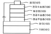
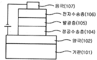
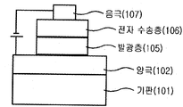
- FIGS. 1 to 6 The structure of the organic light emitting display device according to another embodiment of the present invention is illustrated in FIGS. 1 to 6, but is not limited thereto.
- reference numeral 101 denotes a substrate, 102 an anode, 103 a hole injection layer (HIL), 104 a hole transport layer (HTL), 105 a light emitting layer (EML), 106 an electron injection layer (EIL), 107 an electron transport layer ( ETL), 108 represents a negative electrode.
- the organic light emitting diode may further include a hole blocking layer (HBL) for blocking the movement of holes, an electron blocking layer (EBL) for preventing the movement of electrons, and a protective layer.
- the protective layer may be formed to protect the organic material layer or the cathode at the uppermost layer.
- the compound including two or more compounds containing two or more five-membered heterocyclic ring described with reference to Formulas 1 to 4 may be included in one or more of an organic material layer including a hole injection layer, a hole transport layer, a light emitting layer and an electron transport layer.
- the compound including two or more compounds containing two or more five-membered heterocyclic ring described with reference to Formulas 1 to 4 is a hole injection layer, a hole transport layer, a light emitting layer, an electron transport layer, an electron injection layer, a hole blocking layer, It may be used in place of one or more of the electronic blocking layer, the protective layer, or may be used by forming a layer with them.
- the organic layer may be used not only in one layer but also in two or more layers.
- Compounds containing two or more compounds containing two or more five-membered heterocycles described with reference to Formulas 1 to 4 may play various roles in the organic electronic device and the terminal, and all of red, green, blue, white, etc. It is useful as a hole injection material, a hole transport material, a light emitting material and / or an electron transport material suitable for color fluorescence and phosphorescent devices, and can be used as a host material for phosphorescent dopants of various colors.
- the organic light emitting device is a metal having a metal or conductivity on a substrate by using a physical vapor deposition (PVD) method such as sputtering or e-beam evaporation
- PVD physical vapor deposition
- An oxide or an alloy thereof is deposited to form an anode, an organic material layer including a hole injection layer, a hole transport layer, a light emitting layer, an electron transport layer, and an electron injection layer is formed thereon, and then a material that can be used as a cathode is deposited thereon.
- PVD physical vapor deposition
- an organic electronic device may be fabricated by sequentially depositing a cathode material, an organic material layer, and an anode material on a substrate.
- the organic material layer may have a multilayer structure including a hole injection layer, a hole transport layer, a light emitting layer, an electron transport layer and an electron injection layer, but is not limited thereto and may have a single layer structure.
- the organic material layer may be formed by using a variety of polymer materials, and by using a process such as spin coating, dip coating, doctor blading, screen printing, inkjet printing, or thermal transfer, rather than a deposition method. It can be prepared in layers.
- An organic light emitting display device forms an organic material layer, for example, a light emitting layer, by a soluble process of a compound containing two or more compounds including two or more five-membered heterocycles described above. You may.
- the substrate is a support of the organic light emitting device, and a silicon wafer, quartz or glass plate, metal plate, plastic film or sheet, or the like can be used.
- An anode is positioned over the substrate. This anode injects holes into the hole injection layer located thereon.
- the anode material a material having a large work function is usually preferred to facilitate hole injection into the organic material layer.
- the positive electrode material that can be used in the present invention include metals such as vanadium, chromium, copper, zinc, gold or alloys thereof; Metal oxides such as zinc oxide, indium oxide, indium tin oxide (ITO), indium zinc oxide (IZO); Combinations of metals and oxides such as ZnO: Al or SnO 2 : Sb; Conductive polymers such as poly (3-methylthiophene), poly [3,4- (ethylene-1,2-dioxy) thiophene] (PEDT), polypyrrole and polyaniline, and the like, but are not limited thereto.
- the hole injection layer is located on the anode.
- the conditions required for the material of the hole injection layer are high hole injection efficiency from the anode, it should be able to transport the injected holes efficiently. This requires a small ionization potential, high transparency to visible light, and excellent hole stability.
- the hole injection material is a material capable of well injecting holes from the anode at low voltage, and the highest occupied molecular orbital (HOMO) of the hole injection material is preferably between the work function of the positive electrode material and the HOMO of the surrounding organic material layer.
- hole injection materials include metal porphyrine, oligothiophene, arylamine-based organics, hexanitrile hexaazatriphenylene, quinacridone-based organics, perylene-based organics, Anthraquinone, polyaniline and polythiophene-based conductive polymers, but are not limited thereto.
- the hole transport layer is positioned on the hole injection layer.
- the hole transport layer receives holes from the hole injection layer and transports the holes to the organic light emitting layer located thereon, and serves to prevent high hole mobility, hole stability, and electrons.
- applications for vehicle body display require heat resistance to the device, and materials having a glass transition temperature (Tg) of 70 or greater are preferred.
- Materials satisfying these conditions include NPD (or NPB), spiro-arylamine compounds, perylene-arylamine compounds, azacycloheptatriene compounds, bis (diphenylvinylphenyl) anthracene and silicon germanium oxide.
- Tg glass transition temperature
- Materials satisfying these conditions include NPD (or NPB), spiro-arylamine compounds, perylene-arylamine compounds, azacycloheptatriene compounds, bis (diphenylvinylphenyl) anthracene and silicon germanium oxide.
- the organic light emitting layer is positioned on the hole transport layer.
- the organic light emitting layer is a layer for emitting light by recombination of holes and electrons injected from the anode and the cathode, respectively, and is made of a material having high quantum efficiency.
- the light emitting material is a material capable of emitting light in the visible region by transporting and combining holes and electrons from the hole transport layer and the electron transport layer, respectively, and a material having good quantum efficiency with respect to fluorescence or phosphorescence is preferable.
- Substances or compounds that satisfy these conditions include Alq3 for green, Balq (8-hydroxyquinoline beryllium salt) for blue, DPVBi (4,4'-bis (2,2-diphenylethenyl) -1,1'- biphenyl) series, Spiro material, Spiro-DPVBi (Spiro-4,4'-bis (2,2-diphenylethenyl) -1,1'-biphenyl), LiPBO (2- (2-benzoxazoyl) -phenol lithium salt), bis (diphenylvinylphenylvinyl) benzene, aluminum-quinoline metal complex, metal complexes of imidazole, thiazole and oxazole, and the like, perylene, and BczVBi (3,3 ') to increase blue light emission efficiency.
- an organic light emitting layer is formed of a polymer of polyphenylene vinylene (PPV) or a polymer such as poly fluorene.
- PPV polyphenylene vinylene
- a polymer such as poly fluorene can be used for
- the electron transport layer is positioned on the organic light emitting layer.
- Such an electron transport layer requires a material having high electron injection efficiency and efficiently transporting injected electrons from a cathode positioned thereon. To this end, it must be made of a material having high electron affinity and electron transfer speed and excellent stability to electrons. Examples of the electron transport material that satisfies such conditions include Al complexes of 8-hydroxyquinoline; Complexes including Alq 3 ; Organic radical compounds; Hydroxyflavone-metal complexes and the like, but are not limited thereto.
- the electron injection layer is stacked on the electron transport layer.
- the electron injection layer is a metal complex compound such as Balq, Alq3, Be (bq) 2, Zn (BTZ) 2, Zn (phq) 2, PBD, spiro-PBD, TPBI, Tf-6P, aromatic compound with imidazole ring, It can be produced using a low molecular weight material containing boron compounds and the like.
- the electron injection layer may be formed in a thickness range of 100 ⁇ 300.
- the cathode is positioned on the electron injection layer. This cathode serves to inject electrons.
- the material used as the cathode it is possible to use the material used for the anode, and a metal having a low work function is more preferable for efficient electron injection.
- a suitable metal such as tin, magnesium, indium, calcium, sodium, lithium, aluminum, silver, or a suitable alloy thereof can be used.
- an electrode having a two-layer structure such as lithium fluoride and aluminum, lithium oxide and aluminum, strontium oxide and aluminum having a thickness of 100 or less can also be used.
- holes suitable for fluorescence and phosphorescent devices of all colors such as red, green, blue, and white, depending on the compound including two or more compounds including two or more five-membered heterocycles described with reference to Chemical Formulas 1 to 12 It can be used as an injection material, a hole transport material, a light emitting material, an electron transport material and an electron injection material, and can be used as a host material for phosphorescent dopants of various colors.
- the organic light emitting device may be a top emission type, a bottom emission type or a double-sided emission type according to the material used.
- the present invention includes a display device including the organic electric element described above, and a terminal including a control unit for driving the display device.
- This terminal means a current or future wired or wireless communication terminal.
- the terminal according to the present invention described above may be a mobile communication terminal such as a mobile phone, and includes all terminals such as a PDA, an electronic dictionary, a PMP, a remote control, a navigation device, a game machine, various TVs, various computers, and the like.
- step 1 The intermediate A obtained in step 1) was dissolved in anhydrous THF, the temperature of the reaction was lowered to 8, n-BuLi (1.6 M in hexane) was slowly added dropwise, and the reaction was stirred at 0 to 1 hour. The temperature of the reaction was lowered to -78, Isopropoxy-4,4,5,5-tetramethyl-1,3,2-dioxaborolane was added dropwise and stirred at room temperature for 12 hours. After completion of the reaction, the mixture was extracted with CH 2 Cl 2 , water was removed from the reaction with anhydrous MgSO 4 , filtered under reduced pressure, and the organic solvent was concentrated to give the resulting product as methyl alcohol.
- n-BuLi 1.6 M in hexane
- the intermediate A, 9-Anthraceneboronic acid, Pd (PPh 3 ) 4 and K 2 CO 3 synthesized in step 1) were dissolved in anhydrous THF and a small amount of water, and then refluxed for 24 hours. After the reaction was completed, the reaction was cooled to room temperature, extracted with CH 2 Cl 2 , and washed with water. After removal of a small amount of water with anhydrous MgSO 4 and filtration under reduced pressure, the organic solvent was concentrated and the resulting product was recrystallized using a toluene solvent to give the desired compound 10 (yield: 71%).
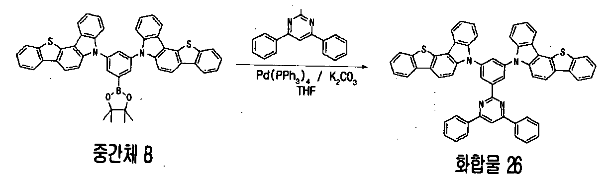
- the intermediate B, 2-Iodo-4,6-diphenylpyrimidine, Pd (PPh 3 ) 4 and K 2 CO 3 synthesized in step 2) were dissolved in anhydrous THF and a small amount of water, and then refluxed for 24 hours. After the reaction was completed, the reaction was cooled to room temperature, extracted with CH 2 Cl 2 , and washed with water. After removal of a small amount of water with anhydrous MgSO 4 and filtration under reduced pressure, the organic solvent was concentrated and the resulting product was recrystallized using a toluene solvent to give the desired compound 26 (yield: 54%).
- the compounds represented by Formulas 1 to 3 are R 1 , R 2 , R 3 , R 4 , R 5 , R 6 , R 7 , R 8 , R 9 , R 10 , R 1 ', R 2 ', R 3
- Substituted or unsubstituted substituents of the substituents of ', R 4 ', R 5 ', R 6 ', R 7 ', R 8 ', R 9 ', and R 10 ' are compounds represented by the general formula (4) in a broad relationship. Synthesis examples of some of the above, but the compounds represented by the formula (1) to 4 not illustratively described as a synthesis example may also form part of the present specification.
- a copper phthalocyanine (hereinafter abbreviated as CuPc) film was vacuum-deposited on the ITO layer (anode) formed on the glass substrate to form a thickness of 10 nm.
- a-NPD 4,4-bis [N- (1-naphthyl) -N-phenylamino] biphenyl
- compounds 10, 26, 38, and 56 were deposited on the hole transport layer as phosphorescent host materials to form a light emitting layer.
- tris (2-phenylpyridine) iridium (abbreviated as I r (ppy) 3 hereinafter) was added as a phosphorescent Ir metal complex dopant.
- concentration of I r (ppy) 3 in the light emitting layer was 5% by weight.
- (1,1-bisphenyl) -4-oleato) bis (2-methyl-8-quinolinoleito) aluminum (hereinafter abbreviated as BAlq) was vacuum-deposited to a thickness of 10 nm as a hole blocking layer, followed by electrons.
- Tris (8-quinolinol) aluminum (hereinafter abbreviated to Alq 3 ) was formed into an injection layer to a thickness of 40 nm.
- LiF an alkali metal halide
- Al was deposited to a thickness of 150 nm to use an Al / LiF as a cathode to prepare an organic light emitting device.
- an organic electroluminescent device having the same structure as the test example was manufactured using a compound represented by Chemical Formula 13 (hereinafter abbreviated as CBP) as a light emitting host material instead of the compound of the present invention.
- CBP Chemical Formula 13
- the organic electroluminescent device using the organic electroluminescent device material of the present invention is not only excellent in the luminous efficiency compared to the CBP used as a comparative example, Since green light emission is obtained in which color purity is remarkably improved, it is used as a phosphorescent host material of an organic light emitting display device, and thus light emission efficiency and color purity may be remarkably improved.
- the compounds of the present invention are used in other organic material layers of the organic light emitting device, for example, the host material of the light emitting layer, as well as the electron injection layer, the electron transport layer, the hole injection layer and the hole transport layer.
- the compounds represented by Formulas 1 to 4 are R 1 , R 2 , R 3 , R 4 , R 5 , R 6 , R 7 , R 8 , R 9 , R 10 , R 1 ', R 2 ', R 3
- Substituted or unsubstituted substituents of ', R 4 ', R 5 ', R 6 ', R 7 ', R 8 ', R 9 ', and R 10 ' are some of the compounds represented by the formula (4) in a broad relationship.
Landscapes
- Chemical & Material Sciences (AREA)
- Organic Chemistry (AREA)
- Physics & Mathematics (AREA)
- Spectroscopy & Molecular Physics (AREA)
- Engineering & Computer Science (AREA)
- Materials Engineering (AREA)
- Electroluminescent Light Sources (AREA)
- Nitrogen Condensed Heterocyclic Rings (AREA)
- Heterocyclic Carbon Compounds Containing A Hetero Ring Having Oxygen Or Sulfur (AREA)
Abstract
Provided are a compound comprising at least two compounds comprising at least two five-membered hetero rings, an organic electrical element using the same and a terminal thereof.
Description
본 발명은 2개 이상의 오원자 헤테로고리를 포함하는 화합물이 2개 이상 포함하는 화합물 및 이를 이용한 유기전기소자, 그 단말에 관한 것이다. The present invention relates to a compound comprising two or more compounds containing two or more five-membered heterocycles, an organic electric device using the same, and a terminal thereof.
일반적으로 유기 발광 현상이란 유기 물질을 이용하여 전기에너지를 빛에너지로 전환시켜주는 현상을 말한다. 유기 발광 현상을 이용하는 유기전기소자는 통상 양극과 음극 및 이 사이에 유기물층을 포함하는 구조를 가진다. 여기서 유기물층은 유기전기소자의 효율과 안정성을 높이기 위하여 각기 다른 물질로 구성된 다층의 구조로 이루어진 경우가 많으며, 예컨대 정공주입층, 정공수송층, 발광층, 전자수송층 및 전자주입층 등으로 이루어질 수 있다.In general, organic light emitting phenomenon refers to a phenomenon of converting electrical energy into light energy using an organic material. An organic electric element using an organic light emitting phenomenon usually has a structure including an anode, a cathode, and an organic material layer therebetween. In this case, the organic material layer is often formed of a multi-layered structure composed of different materials in order to increase the efficiency and stability of the organic electric device, for example, it may be made of a hole injection layer, a hole transport layer, a light emitting layer, an electron transport layer and an electron injection layer.
유기전기소자에서 유기물층으로 사용되는 재료는 기능에 따라, 발광 재료와 전하 수송 재료, 예컨대 정공주입 재료, 정공수송 재료, 전자수송 재료, 전자주입 재료 등으로 분류될 수 있다. 그리고, 상기 발광 재료는 분자량에 따라 고분자형과 저분자형으로 분류될 수 있고, 발광 메커니즘에 따라 전자의 일중항 여기상태로부터 유래되는 형광 재료와 전자의 삼중항 여기상태로부터 유래되는 인광 재료로 분류될 수 있다. 또한, 발광 재료는 발광색에 따라 청색, 녹색, 적색 발광 재료와 보다 나은 천연색을 구현하기 위해 필요한 노란색 및 주황색 발광 재료로 구분될 수 있다.Materials used as the organic material layer in the organic electric element may be classified into light emitting materials and charge transport materials, such as hole injection materials, hole transport materials, electron transport materials, electron injection materials, and the like, depending on their functions. The light emitting material may be classified into a polymer type and a low molecular type according to molecular weight, and may be classified into a fluorescent material derived from a singlet excited state of electrons and a phosphorescent material derived from a triplet excited state of electrons according to a light emitting mechanism. Can be. In addition, the light emitting material may be classified into blue, green, and red light emitting materials and yellow and orange light emitting materials required to achieve a better natural color according to the light emitting color.
한편, 발광 재료로서 하나의 물질만 사용하는 경우 분자간 상호 작용에 의하여 최대 발광 파장이 장파장으로 이동하고 색순도가 떨어지거나 발광 감쇄 효과로 소자의 효율이 감소되는 문제가 발생하므로, 색순도의 증가와 에너지 전이를 통한 발광 효율을 증가시키기 위하여 발광 재료로서 호스트/도판트 계를 사용할 수 있다. 그 원리는 발광층을 형성하는 호스트 보다 에너지 대역 간극이 작은 도판트를 발광층에 소량 혼합하면, 발광층에서 발생한 엑시톤이 도판트로 수송되어 효율이 높은 빛을 내는 것이다. 이 때 호스트의 파장이 도판트의 파장대로 이동하므로, 이용하는 도판트의 종류에 따라 원하는 파장의 빛을 얻을 수 있다.On the other hand, when only one material is used as the light emitting material, the maximum emission wavelength is shifted to a long wavelength due to the intermolecular interaction, and the color purity decreases or the efficiency of the device decreases due to the emission attenuation effect. In order to increase the light emitting efficiency through the light emitting material, a host / dopant system may be used. The principle is that when a small amount of dopant having an energy band gap smaller than that of a host forming the light emitting layer is mixed in the light emitting layer, excitons generated in the light emitting layer are transported to the dopant, thereby producing high-efficiency light. At this time, since the wavelength of the host shifts to the wavelength of the dopant, light having a desired wavelength can be obtained according to the type of dopant to be used.
전술한 유기전기소자가 갖는 우수한 특징들을 충분히 발휘하기 위해서는 소자내 유기물층을 이루는 물질, 예컨대 정공주입 물질, 정공수송 물질, 발광 물질, 전자수송 물질, 전자주입 물질 등이 안정하고 효율적인 재료에 의하여 뒷받침되는 것이 선행되어야 하나, 아직까지 안정하고 효율적인 유기전기소자용 유기물층 재료의 개발이 충분히 이루어지지 않은 상태이며, 따라서 새로운 재료의 개발이 계속 요구되고 있다.In order to fully exhibit the excellent characteristics of the above-described organic electroluminescent device, a material forming the organic material layer in the device, such as a hole injection material, a hole transport material, a light emitting material, an electron transport material, an electron injection material, etc., is supported by a stable and efficient material. Although this should be preceded, the development of a stable and efficient organic material layer for an organic electric element has not yet been made sufficiently, and therefore, the development of new materials is continuously required.
본 발명자들은 신규한 구조를 갖는 오원자 헤테로 고리를 포함하는 화합물을 밝혀내었으며, 또한 이 화합물을 유기전기소자에 적용시 소자의 발광효율, 안정성 및 수명을 크게 향상시킬 수 있다는 사실을 밝혀내었다.The present inventors have found a compound containing a five-membered heterocyclic ring having a novel structure, and also found that when the compound is applied to an organic electric device, the luminous efficiency, stability and lifetime of the device can be greatly improved.
이에 본 발명은 신규한 오원자 헤테로 고리를 포함하는 화합물 및 이를 이용한 유기전기소자, 그 단말을 제공하는 것을 목적으로 한다.Accordingly, an object of the present invention is to provide a compound containing a novel five-membered hetero ring, an organic electric device using the same, and a terminal thereof.
일측면에서, 본 발명은 아래 화학식으로 표시되는 화합물을 제공한다.In one aspect, the present invention provides a compound represented by the following formula.

본 발명은 2개 이상의 오원자 헤테로고리를 포함하는 화합물이 2개 이상 포함하는 화합물에 따라서 적색, 녹색, 청색, 흰색 등의 모든 칼라의 형광과 인광소자에 적합한 정공주입 재료, 정공수송 재료, 발광 재료 및/또는 전자수송 재료로 유용하며, 다양한 색의 인광 도판트의 호스트 물질로 유용하다.The present invention provides a hole injection material, a hole transport material, a light emitting device suitable for fluorescence and phosphorescent devices of all colors, such as red, green, blue, white, etc., according to a compound including two or more five or more heteroatomic heterocycles. It is useful as a material and / or electron transport material, and as a host material for phosphorescent dopants of various colors.
또한, 본 발명은 상기의 화학식을 가지는 화합물을 이용한 유기 전자 소자 및 이 유기 전자 소자를 포함하는 단말을 제공한다.The present invention also provides an organic electronic device using the compound having the above formula and a terminal including the organic electronic device.
2개 이상의 오원자 헤테로고리를 포함하는 화합물이 2개 이상 포함하는 화합물은 유기전기소자 및 단말에서 다양한 역할을 할 수 있으며, 적색, 녹색, 청색, 흰색 등의 모든 칼라의 형광과 인광소자에 적합한 정공주입 재료, 정공수송 재료, 발광 재료 및/또는 전자수송 재료로 유용하며, 다양한 색의 인광 도판트의 호스트 물질로 유용하다.Compounds containing two or more compounds containing two or more five-membered heterocycles may play various roles in organic electronic devices and terminals, and are suitable for fluorescent and phosphorescent devices of all colors such as red, green, blue, and white. It is useful as a hole injection material, a hole transport material, a light emitting material and / or an electron transport material, and is useful as a host material for phosphorescent dopants of various colors.
도 1 내지 도 6은 본 발명의 화합물을 적용할 수 있는 유기전계발광소자의 예를 도시한 것이다.1 to 6 show examples of the organic light emitting display device to which the compound of the present invention can be applied.
이하, 본 발명의 일부 실시예들을 예시적인 도면을 통해 상세하게 설명한다. 각 도면의 구성요소들에 참조부호를 부가함에 있어서, 동일한 구성요소들에 대해서는 비록 다른 도면상에 표시되더라도 가능한 한 동일한 부호를 가지도록 하고 있음에 유의해야 한다. 또한, 본 발명을 설명함에 있어, 관련된 공지 구성 또는 기능에 대한 구체적인 설명이 본 발명의 요지를 흐릴 수 있다고 판단되는 경우에는 그 상세한 설명은 생략한다.Hereinafter, some embodiments of the present invention will be described in detail through exemplary drawings. In adding reference numerals to the components of each drawing, it should be noted that the same reference numerals are assigned to the same components as much as possible even though they are shown in different drawings. In addition, in describing the present invention, when it is determined that the detailed description of the related well-known configuration or function may obscure the gist of the present invention, the detailed description thereof will be omitted.
또한, 본 발명의 구성 요소를 설명하는 데 있어서, 제 1, 제 2, A, B, (a), (b) 등의 용어를 사용할 수 있다. 이러한 용어는 그 구성 요소를 다른 구성 요소와 구별하기 위한 것일 뿐, 그 용어에 의해 해당 구성 요소의 본질이나 차례 또는 순서 등이 한정되지 않는다. 어떤 구성 요소가 다른 구성요소에 "연결", "결합" 또는 "접속"된다고 기재된 경우, 그 구성 요소는 그 다른 구성요소에 직접적으로 연결되거나 또는 접속될 수 있지만, 각 구성 요소 사이에 또 다른 구성 요소가 "연결", "결합" 또는 "접속"될 수도 있다고 이해되어야 할 것이다.In addition, in describing the component of this invention, terms, such as 1st, 2nd, A, B, (a), (b), can be used. These terms are only for distinguishing the components from other components, and the nature, order or order of the components are not limited by the terms. If a component is described as being "connected", "coupled" or "connected" to another component, that component may be directly connected to or connected to that other component, but there may be another configuration between each component. It is to be understood that the elements may be "connected", "coupled" or "connected".
일측면에서, 본 발명은 아래 화학식 1로 표시되는 화합물을 제공한다. In one aspect, the present invention provides a compound represented by the following formula (1).
[화학식 1][Formula 1]

위 화학식 1에 있어서, In Chemical Formula 1,
(1) R1, R2, R3, R4, R5, R6, R7, R8, R9, R10, R1', R2', R3', R4 ', R5', R6', R7', R8', R9', 및 R10'은 각각 서로 독립적으로 수소 원자, 할로겐 원자, 시아노기, 알콕시기, 티올기, 치환 또는 비치환된 탄소수 1 내지 50의 알킬기, 치환 또는 비치환된 탄소수 1 내지 50의 알콕시기, 치환 또는 비치환의 탄소수 1 내지 50의 알케닐기, 치환 또는 비치환의 탄소수 5 내지 60의 아릴렌기, 치환 또는 비치환된 탄소수 5 내지 60의 아릴기, 치환 또는 비치환된 탄소수 5 내지 60의 아릴옥시기, 황(S), 질소(N), 산소(O), 인(P) 및 규소(Si)를 적어도 하나 이상 포함하는 치환 또는 비치환된 탄소수 1 내지 50의 알킬기 또는 황(S), 질소(N), 산소(O), 인(P) 및 규소(Si)를 적어도 하나 이상 포함하는 치환 또는 비치환된 탄소수 5 내지 60의 헤테로아릴기 또는 황(S), 질소(N), 산소(O), 인(P) 및 규소(Si)를 적어도 하나 이상 포함하는 치환 또는 비치환된 탄소수 5 내지 60의 헤테로아릴옥시기일 수 있다.(1) R 1 , R 2 , R 3 , R 4 , R 5 , R 6 , R 7 , R 8 , R 9 , R 10 , R 1 ', R 2 ', R 3 ', R 4 ', R 5 ′, R 6 ′, R 7 ′, R 8 ′, R 9 ′, and R 10 ′ each independently represent a hydrogen atom, a halogen atom, a cyano group, an alkoxy group, a thiol group, a substituted or unsubstituted carbon number 1 An alkyl group of 50 to 50, a substituted or unsubstituted alkoxy group of 1 to 50 carbon atoms, a substituted or unsubstituted alkenyl group of 1 to 50 carbon atoms, a substituted or unsubstituted arylene group of 5 to 60 carbon atoms, a substituted or unsubstituted carbon number 5 to Substitutes containing at least one aryl group of 60, a substituted or unsubstituted aryloxy group having 5 to 60 carbon atoms, sulfur (S), nitrogen (N), oxygen (O), phosphorus (P) and silicon (Si) Or a substituted or unsubstituted C 5 to 60 carbon atoms containing at least one unsubstituted alkyl group having 1 to 50 carbon atoms or sulfur (S), nitrogen (N), oxygen (O), phosphorus (P) and silicon (Si). Heteroaryl group or sulfur (S), nitrogen (N), oxygen (O), (P) and a silicon (Si) can heteroaryloxy substituted or unsubstituted carbon atoms of 5 to 60 ring date, including at least one.
(2) R1 내지 R10 및 R1' 내지 R10'은 인접한 기와 결합하여 포화 또는 불포화고리를 형성할 수 있다. 예를 들어 이웃하는 R1과 R2, R2와 R3, ...R8과 R9, R9와 R10이 결합하여 포화 또는 불포화고리를 형성할 수 있다. 예를 들어 이웃하는 R1'과 R2', R2'와 R3', ...R8'과 R9', R9'와 R10'이 결합하여 포화 또는 불포화고리를 형성할 수 있다. (2) R 1 to R 10 and R 1 ′ to R 10 ′ may combine with adjacent groups to form a saturated or unsaturated ring. For example, neighboring R 1 and R 2 , R 2 and R 3 , ... R 8 and R 9 , R 9 and R 10 may combine to form a saturated or unsaturated ring. For example, neighboring R 1 'and R 2 ', R 2 'and R 3 ', ... R 8 'and R 9 ', R 9 'and R 10 ' may combine to form a saturated or unsaturated ring have.
(3) X는 탄소(C) 또는 질소(N)일 수 있다.(3) X may be carbon (C) or nitrogen (N).
(4) Ar은 수소 원자, 할로겐 원자, 시아노기, 알콕시기, 티올기, 치환 또는 비치환된 탄소수 1 내지 50의 알킬기, 치환 또는 비치환의 탄소수 1 내지 50의 알케닐기, 치환 또는 비치환의 탄소수 5 내지 60의 아릴렌기, 치환 또는 비치환된 탄소수 5 내지 60의 아릴기, 치환 또는 비치환된 탄소수 5 내지 60의 아릴옥시기, 황(S), 질소(N), 산소(O), 인(P) 및 규소(Si)를 적어도 하나 이상 포함하는 치환 또는 비치환된 탄소수 1 내지 50의 알킬기 또는 황(S), 질소(N), 산소(O), 인(P) 및 규소(Si)를 적어도 하나 이상 포함하는 치환 또는 비치환된 탄소수 5 내지 60의(4) Ar represents a hydrogen atom, a halogen atom, a cyano group, an alkoxy group, a thiol group, a substituted or unsubstituted alkyl group having 1 to 50 carbon atoms, a substituted or unsubstituted alkenyl group having 1 to 50 carbon atoms, a substituted or unsubstituted carbon number 5 To 60 arylene group, substituted or unsubstituted aryl group having 5 to 60 carbon atoms, substituted or unsubstituted aryloxy group having 5 to 60 carbon atoms, sulfur (S), nitrogen (N), oxygen (O), phosphorus ( A substituted or unsubstituted alkyl group having 1 to 50 carbon atoms or at least one of P) and silicon (Si) or sulfur (S), nitrogen (N), oxygen (O), phosphorus (P) and silicon (Si); Substituted or unsubstituted C 5 to 60 containing at least one or more
헤테로아릴기 또는 황(S), 질소(N), 산소(O), 인(P) 및 규소(Si)를 적어도 하나 이상 포함하는 치환 또는 비치환된 탄소수 5 내지 60의 헤테로아릴옥시기일 수 있다.Heteroaryl group or substituted or unsubstituted heteroaryloxy group having 5 to 60 carbon atoms containing at least one or more sulfur (S), nitrogen (N), oxygen (O), phosphorus (P) and silicon (Si). .
(5) 상기 구조식을 가지는 화합물은 용액 공정(soluble process)에 사용될 수 있다. 즉, 상기 화합물로 용액 공정(soluble process)에 의해 후술할 유기전기소자의 유기물층을 형성할 수 있다. 즉 유기전기소자의 유기물층은 다양한 고분자 소재를 사용하여 증착법이 아닌 솔벤트 프로세스(solvent process), 예컨대 스핀 코팅, 딥 코팅, 닥터 블레이딩, 스크린 프린팅, 잉크젯 프린팅 또는 열 전사법 등의 방법에 의하여 더 적은 수의 층으로 제조할 수 있다.(5) The compound having the above structural formula can be used in a soluble process. That is, the organic material layer of the organic electric device, which will be described later, may be formed by a soluble process using the compound. In other words, the organic material layer of the organic electronic device is made by using a variety of polymer materials, and less by a solvent process (e.g., spin coating, dip coating, doctor blading, screen printing, inkjet printing or thermal transfer method) rather than deposition. It can be prepared in a number of layers.
다른 측면에서, 본 발명은 아래 화학식 2로 표시되는 화합물을 제공한다. In another aspect, the present invention provides a compound represented by the following formula (2).
[화학식 2][Formula 2]

또다른 측면에서, 본 발명은 아래 화학식 3으로 표시되는 화합물을 제공한다. In another aspect, the present invention provides a compound represented by the formula (3) below.
[화학식 3][Formula 3]

위 화학식 2 및 3에서 Ar은 화학식 1과 동일하다. Ar in Formulas 2 and 3 is the same as in Formula 1.
위 화학식 1 내지 3에서 R1, R2, R3, R4, R5, R6, R7, R8, R9, R10, R1', R2', R3', R4 ', R5', R6', R7', R8', R9', 및 R10' 의 치환기들은 치환 또는 비치환될 수 있은데 치환된 경우 각각 독립적으로 각각 서로 독립적으로 수소 원자, 할로겐 원자, 시아노기, 알콕시기, 티올기, 치환 또는 비치환된 탄소수 1 내지 50의 알킬기, 치환 또는 비치환된 탄소수 1 내지 50의 알콕시기, 치환 또는 비치환의 탄소수 1 내지 50의 알케닐기, 치환 또는 비치환의 탄소수 5 내지 60의 아릴렌기, 치환 또는 비치환된 탄소수 5 내지 60의 아릴기, 치환 또는 비치환된 탄소수 5 내지 60의 아릴옥시기, 황(S), 질소(N), 산소(O), 인(P) 및 규소(Si)를 적어도 하나 이상 포함하는 치환 또는 비치환된 탄소수 1 내지 50의 알킬기 또는 황(S), 질소(N), 산소(O), 인(P) 및 규소(Si)를 적어도 하나 이상 포함하는 치환 또는 비치환된 탄소수 5 내지 60의 헤테로아릴기 또는 황(S), 질소(N), 산소(O), 인(P) 및 규소(Si)를 적어도 하나 이상 포함하는 치환 또는 비치환된 탄소수 5 내지 60의 헤테로아릴옥시기이루어진 군으로부터 선택된 하나로 치환될 수 있다. In Formulas 1 to 3, R 1 , R 2 , R 3 , R 4 , R 5 , R 6 , R 7 , R 8 , R 9 , R 10 , R 1 ', R 2 ', R 3 ', R 4 Substituents of ', R 5 ', R 6 ', R 7 ', R 8 ', R 9 ', and R 10 'may be substituted or unsubstituted. When substituted, each independently of each other, a hydrogen atom, Halogen atom, cyano group, alkoxy group, thiol group, substituted or unsubstituted alkyl group having 1 to 50 carbon atoms, substituted or unsubstituted alkoxy group having 1 to 50 carbon atoms, substituted or unsubstituted alkenyl group having 1 to 50 carbon atoms, substitution Or an unsubstituted arylene group having 5 to 60 carbon atoms, a substituted or unsubstituted aryl group having 5 to 60 carbon atoms, a substituted or unsubstituted aryloxy group having 5 to 60 carbon atoms, sulfur (S), nitrogen (N), oxygen ( A substituted or unsubstituted alkyl group having 1 to 50 carbon atoms or sulfur (S), nitrogen (N), oxygen (O), phosphorus (P) and at least one of O), phosphorus (P) and silicon (Si); At least one silicon (Si) Substituted or unsubstituted containing at least one substituted or unsubstituted heteroaryl group having 5 to 60 carbon atoms or sulfur (S), nitrogen (N), oxygen (O), phosphorus (P) and silicon (Si) It may be substituted with one selected from the group consisting of a heteroaryloxy group having 5 to 60 carbon atoms.
본 발명의 일실시예에 따른 2개 이상의 오원자 헤테로고리를 포함하는 화합물이 2개 이상 포함하는 화합물인 화학식 1 내지 3에 속하는 화합물의 구체적 예로서 아래 화학식 4의 화합물들이 있으나, 본 발명이 이들에만 한정되는 것은 아니다. 아래 화학식 4의 화합물들은 R1 내지 R10 및 R1' 내지 R10'가 수소 원자인 것으로 표시하였으나 화학식 1 내지 3에서 설명한 다른 작용기일 수도 있다. Specific examples of the compounds belonging to Chemical Formulas 1 to 3, which are compounds including two or more five-membered heterocyclic rings, according to one embodiment of the present invention include the compounds of Formula 4 below, but the present invention It is not limited only to. The compounds of Formula 4 below are represented by R 1 to R 10 and R 1 'to R 10 ' are hydrogen atoms, but may be other functional groups described in Formulas 1 to 3.
다시말해 이때 화학식1 내지 3로 표시되는 화합물들은 R1, R2, R3, R4, R5, R6, R7, R8, R9, R10, R1', R2', R3', R4 ', R5', R6', R7', R8', R9', 및 R10' 의 치환기들의 치환 또는 비치환된 치환기들은 광범위한 관계로 모든 화합물들을 예시하는 것은 현실적으로 어려우므로 대표적인 화합물들을 예시적으로 설명하나 화학식 4에 설명하지 않은 화학식 1 내지 3로 표시되는 화합물들도 본 명세서의 일부를 구성할 수 있다.In other words, the compounds represented by Formulas 1 to 3 may be represented by R 1 , R 2 , R 3 , R 4 , R 5 , R 6 , R 7 , R 8 , R 9 , R 10 , R 1 ', R 2 ', Substituted or unsubstituted substituents of the substituents of R 3 ′, R 4 ′, R 5 ′, R 6 ′, R 7 ′, R 8 ′, R 9 ′, and R 10 ′ exemplify all compounds in a broad context. Since it is difficult to realistically describe exemplary compounds by way of example, the compounds represented by Chemical Formulas 1 to 3 not described in Chemical Formula 4 may also form part of the present specification.
[화학식 4][Formula 4]


화학식 1 내지 4를 참조하여 설명한 2개 이상의 오원자 헤테로고리를 포함하는 화합물이 2개 이상 포함하는 화합물들이 유기물층으로 사용되는 다양한 유기전기소자들이 존재한다. 화학식 1 내지 4를 참조하여 설명한 2개 이상의 오원자 헤테로고리를 포함하는 화합물이 2개 이상 포함하는 화합물들이 사용될 수 있는 유기전기소자는 예를 들어, 유기전계발광소자(OLED), 유기태양전지, 유기감광체(OPC) 드럼, 유기트랜지스트(유기 TFT), 포토다이오드(photodiode), 유기레이저(organic laser), 레이저 다이오드(laser diode) 등이 있다.Various organic electric devices exist in which compounds including two or more compounds including two or more five-membered heterocycles described with reference to Chemical Formulas 1 to 4 are used as the organic material layer. Examples of organic electroluminescent devices in which compounds including two or more compounds including two or more five-membered heterocycles described with reference to Chemical Formulas 1 and 4 may be used include, for example, an organic light emitting diode (OLED), an organic solar cell, Organophotoreceptor (OPC) drums, organic transistors (organic TFTs), photodiodes, organic lasers, laser diodes, and the like.
화학식 1 내지 4를 참조하여 설명한 2개 이상의 오원자 헤테로고리를 포함하는 화합물이 2개 이상 포함하는 화합물들이 적용될 수 있는 유기전기소자 중 일예로 유기전계발광소자(OLED)에 대하여 아래 설명하나, 본 발명은 이에 제한되지 않고 다양한 유기전기소자에 위에서 설명한 2개 이상의 오원자 헤테로고리를 포함하는 화합물이 2개 이상 포함하는 화합물이 적용될 수 있다.One example of an organic electroluminescent device to which compounds including two or more five-membered heterocyclic rings described with reference to Chemical Formulas 1 to 4 may be applied is described below. The present invention is not limited thereto, and a compound including two or more compounds including two or more five-membered heterocycles described above may be applied to various organic electric devices.
본 발명의 다른 실시예는 제1 전극, 제2 전극 및 이들 전극 사이에 배치된 유기물층을 포함하는 유기전기소자에 있어서, 상기 유기물층 중 1층 이상이 상기 화학식 1 내지 4의 화합물들을 포함하는 유기전계발광소자를 제공한다.Another embodiment of the present invention is an organic electric device comprising a first electrode, a second electrode and an organic material layer disposed between these electrodes, wherein at least one layer of the organic material layer comprises an organic electric field comprising the compounds of Formulas 1 to 4 Provided is a light emitting device.
도 1 내지 도 6은 본 발명의 화합물을 적용할 수 있는 유기전계발광소자의 예를 도시한 것이다.1 to 6 show examples of the organic light emitting display device to which the compound of the present invention can be applied.
본 발명의 다른 실시예에 따른 유기전계발광소자는, 정공주입층, 정공수송층, 발광층, 전자수송층 및 전자주입층을 포함하는 유기물층 중 1층 이상을 상기 화학식 1 내지 6의 화합물들을 포함하도록 형성하는 것을 제외하고는, 당 기술 분야에 통상의 제조 방법 및 재료를 이용하여 당 기술 분야에 알려져 있는 구조로 제조될 수 있다.In an organic light emitting display device according to another embodiment of the present invention, at least one layer of an organic material layer including a hole injection layer, a hole transport layer, a light emitting layer, an electron transport layer and an electron injection layer is formed to include the compounds of Formulas 1 to 6 above. Except for the above, it may be manufactured in a structure known in the art using conventional manufacturing methods and materials in the art.
본 발명에 다른 실시예에 따른 유기전계발광소자의 구조는 도 1 내지 6에 예시되어 있으나, 이들 구조에만 한정된 것은 아니다. 이때, 도면번호 101은 기판, 102는 양극, 103는 정공주입층(HIL), 104는 정공수송층(HTL), 105는 발광층(EML), 106은 전자주입층(EIL), 107은 전자수송층(ETL), 108은 음극을 나타낸다. 미도시하였지만, 이러한 유기전계발광소자는 정공의 이동을 저지하는 정공저지층(HBL), 전자의 이동을 저지하는 전자저지층(EBL) 및 보호층이 더 위치할 수도 있다. 보호층의 경우 최상위층에서 유기물층을 보호하거나 음극을 보호하도록 형성될 수 있다.The structure of the organic light emitting display device according to another embodiment of the present invention is illustrated in FIGS. 1 to 6, but is not limited thereto. In this case, reference numeral 101 denotes a substrate, 102 an anode, 103 a hole injection layer (HIL), 104 a hole transport layer (HTL), 105 a light emitting layer (EML), 106 an electron injection layer (EIL), 107 an electron transport layer ( ETL), 108 represents a negative electrode. Although not shown, the organic light emitting diode may further include a hole blocking layer (HBL) for blocking the movement of holes, an electron blocking layer (EBL) for preventing the movement of electrons, and a protective layer. The protective layer may be formed to protect the organic material layer or the cathode at the uppermost layer.
이때, 화학식 1 내지 4를 참조하여 설명한 2개 이상의 오원자 헤테로고리를 포함하는 화합물이 2개 이상 포함하는 화합물은 정공주입층, 정공수송층, 발광층 및 전자수송층을 포함하는 유기물층 중 하나 이상에 포함될 수 있다. 구체적으로, 화학식 1 내지 4를 참조하여 설명한 2개 이상의 오원자 헤테로고리를 포함하는 화합물이 2개 이상 포함하는 화합물은 정공주입층, 정공수송층, 발광층, 전자수송층, 전자주입층, 정공저지층, 전자저지층, 보호층 중 하나 이상을 대신하여 사용되거나 이들과 함께 층을 형성하여 사용될 수도 있다. 물론 유기물층 중 한층에만 사용되는 것이 아니라 두층 이상에 사용될 수 있다.In this case, the compound including two or more compounds containing two or more five-membered heterocyclic ring described with reference to Formulas 1 to 4 may be included in one or more of an organic material layer including a hole injection layer, a hole transport layer, a light emitting layer and an electron transport layer. have. Specifically, the compound including two or more compounds containing two or more five-membered heterocyclic ring described with reference to Formulas 1 to 4 is a hole injection layer, a hole transport layer, a light emitting layer, an electron transport layer, an electron injection layer, a hole blocking layer, It may be used in place of one or more of the electronic blocking layer, the protective layer, or may be used by forming a layer with them. Of course, the organic layer may be used not only in one layer but also in two or more layers.
화학식 1 내지 4를 참조하여 설명한 2개 이상의 오원자 헤테로고리를 포함하는 화합물이 2개 이상 포함하는 화합물은 유기전기소자 및 단말에서 다양한 역할을 할 수 있으며, 적색, 녹색, 청색, 흰색 등의 모든 칼라의 형광과 인광소자에 적합한 정공주입 재료, 정공수송 재료, 발광 재료 및/또는 전자수송 재료로 유용하며, 다양한 색의 인광 도판트의 호스트 물질로 사용될 수 있다. Compounds containing two or more compounds containing two or more five-membered heterocycles described with reference to Formulas 1 to 4 may play various roles in the organic electronic device and the terminal, and all of red, green, blue, white, etc. It is useful as a hole injection material, a hole transport material, a light emitting material and / or an electron transport material suitable for color fluorescence and phosphorescent devices, and can be used as a host material for phosphorescent dopants of various colors.
예컨대, 본 발명의 다른 실시예에 따른 유기전계발광소자는 스퍼터링(sputtering)이나 전자빔 증발(e-beam evaporation)과 같은 PVD(physical vapor deposition) 방법을 이용하여, 기판 상에 금속 또는 전도성을 가지는 금속 산화물 또는 이들의 합금을 증착시켜 양극을 형성하고, 그 위에 정공주입층, 정공수송층, 발광층, 전자수송층 및 전자주입층을 포함하는 유기물층을 형성한 후, 그 위에 음극으로 사용할 수 있는 물질을 증착시킴으로써 제조될 수 있다.For example, the organic light emitting device according to another embodiment of the present invention is a metal having a metal or conductivity on a substrate by using a physical vapor deposition (PVD) method such as sputtering or e-beam evaporation An oxide or an alloy thereof is deposited to form an anode, an organic material layer including a hole injection layer, a hole transport layer, a light emitting layer, an electron transport layer, and an electron injection layer is formed thereon, and then a material that can be used as a cathode is deposited thereon. Can be prepared.
이와 같은 방법 외에도, 기판 상에 음극 물질부터 유기물층, 양극 물질을 차례로 증착시켜 유기전기소자를 만들 수도 있다. 상기 유기물층은 정공주입층, 정공수송층, 발광층, 전자수송층 및 전자주입층 등을 포함하는 다층 구조일 수도 있으나, 이에 한정되지 않고 단층 구조일 수 있다. 또한, 상기 유기물층은 다양한 고분자 소재를 사용하여 증착법이 아닌 솔벤트 프로세스(solvent process), 예컨대 스핀 코팅, 딥 코팅, 닥터 블레이딩, 스크린 프린팅, 잉크젯 프린팅 또는 열 전사법 등의 방법에 의하여 더 적은 수의 층으로 제조할 수 있다.In addition to the above method, an organic electronic device may be fabricated by sequentially depositing a cathode material, an organic material layer, and an anode material on a substrate. The organic material layer may have a multilayer structure including a hole injection layer, a hole transport layer, a light emitting layer, an electron transport layer and an electron injection layer, but is not limited thereto and may have a single layer structure. In addition, the organic material layer may be formed by using a variety of polymer materials, and by using a process such as spin coating, dip coating, doctor blading, screen printing, inkjet printing, or thermal transfer, rather than a deposition method. It can be prepared in layers.
본 발명의 다른 실시예에 따른 유기전계발광소자는 위에서 설명한 2개 이상의 오원자 헤테로고리를 포함하는 화합물이 2개 이상 포함하는 화합물을 용액 공정(soluble process)에 의해 유기물층, 예를 들어 발광층을 형성할 수도 있다. An organic light emitting display device according to another embodiment of the present invention forms an organic material layer, for example, a light emitting layer, by a soluble process of a compound containing two or more compounds including two or more five-membered heterocycles described above. You may.
기판은 유기전계발광소자의 지지체이며, 실리콘 웨이퍼, 석영 또는 유리판, 금속판, 플라스틱 필름이나 시트 등이 사용될 수 있다.The substrate is a support of the organic light emitting device, and a silicon wafer, quartz or glass plate, metal plate, plastic film or sheet, or the like can be used.
기판 위에는 양극이 위치된다. 이러한 양극은 그 위에 위치되는 정공주입층으로 정공을 주입한다. 양극 물질로는 통상 유기물층으로 정공주입이 원활할 수 있도록 일함수가 큰 물질이 바람직하다. 본 발명에서 사용될 수 있는 양극 물질의 구체적인 예로는 바나듐, 크롬, 구리, 아연, 금과 같은 금속 또는 이들의 합금; 아연산화물, 인듐산화물, 인듐주석 산화물(ITO), 인듐아연산화물(IZO)과 같은 금속 산화물; ZnO:Al 또는 SnO2:Sb와 같은 금속과 산화물의 조합; 폴리(3-메틸티오펜), 폴리[3,4-(에틸렌-1,2-디옥시)티오펜](PEDT), 폴리피롤 및 폴리아닐린과 같은 전도성 고분자 등이 있으나, 이들에만 한정되는 것은 아니다. An anode is positioned over the substrate. This anode injects holes into the hole injection layer located thereon. As the anode material, a material having a large work function is usually preferred to facilitate hole injection into the organic material layer. Specific examples of the positive electrode material that can be used in the present invention include metals such as vanadium, chromium, copper, zinc, gold or alloys thereof; Metal oxides such as zinc oxide, indium oxide, indium tin oxide (ITO), indium zinc oxide (IZO); Combinations of metals and oxides such as ZnO: Al or SnO 2 : Sb; Conductive polymers such as poly (3-methylthiophene), poly [3,4- (ethylene-1,2-dioxy) thiophene] (PEDT), polypyrrole and polyaniline, and the like, but are not limited thereto.
양극 위에는 정공주입층이 위치된다. 이러한 정공주입층의 물질로 요구되는 조건은 양극으로부터의 정공주입 효율이 높으며, 주입된 정공을 효율적으로 수송할 수 있어야 한다. 이를 위해서는 이온화 포텐셜이 작고 가시광선에 대한 투명성이 높으며, 정공에 대한 안정성이 우수해야 한다.The hole injection layer is located on the anode. The conditions required for the material of the hole injection layer are high hole injection efficiency from the anode, it should be able to transport the injected holes efficiently. This requires a small ionization potential, high transparency to visible light, and excellent hole stability.
정공주입 물질로는 낮은 전압에서 양극으로부터 정공을 잘 주입받을 수 있는 물질로서, 정공주입 물질의 HOMO(highest occupied molecular orbital)가 양극 물질의 일함수와 주변 유기물층의 HOMO 사이인 것이 바람직하다. 정공주입 물질의 구체적인 예로는 금속 포피린(porphyrine), 올리고티오펜, 아릴아민 계열의 유기물, 헥사니트릴 헥사아자트리페닐렌, 퀴나크리돈(quinacridone) 계열의 유기물, 페릴렌(perylene) 계열의 유기물, 안트라퀴논 및 폴리아닐린과 폴리티오펜 계열의 전도성 고분자 등이 있으나, 이들에만 한정되는 것은 아니다.The hole injection material is a material capable of well injecting holes from the anode at low voltage, and the highest occupied molecular orbital (HOMO) of the hole injection material is preferably between the work function of the positive electrode material and the HOMO of the surrounding organic material layer. Specific examples of hole injection materials include metal porphyrine, oligothiophene, arylamine-based organics, hexanitrile hexaazatriphenylene, quinacridone-based organics, perylene-based organics, Anthraquinone, polyaniline and polythiophene-based conductive polymers, but are not limited thereto.
상기 정공주입층 위에는 정공수송층이 위치된다. 이러한 정공수송층은 정공주입층으로부터 정공을 전달받아 그 위에 위치되는 유기발광층으로 수송하는 역할을 하며, 높은 정공 이동도와 정공에 대한 안정성 및 전자를 막아주는 역할를 한다. 이러한 일반적 요구 이외에 차체 표시용으로 응용할 경우 소자에 대한 내열성이 요구되며, 유리 전이 온도(Tg)가 70 이상의 값을 갖는 재료가 바람직하다. 이와 같은 조건을 만족하는 물질들로는 NPD(혹은 NPB라 함), 스피로-아릴아민계화합물, 페릴렌-아릴아민계화합물, 아자시클로헵타트리엔화합물, 비스(디페닐비닐페닐)안트라센, 실리콘게르마늄옥사이드화합물, 실리콘계아릴아민화합물 등이 될 수 있다.The hole transport layer is positioned on the hole injection layer. The hole transport layer receives holes from the hole injection layer and transports the holes to the organic light emitting layer located thereon, and serves to prevent high hole mobility, hole stability, and electrons. In addition to these general requirements, applications for vehicle body display require heat resistance to the device, and materials having a glass transition temperature (Tg) of 70 or greater are preferred. Materials satisfying these conditions include NPD (or NPB), spiro-arylamine compounds, perylene-arylamine compounds, azacycloheptatriene compounds, bis (diphenylvinylphenyl) anthracene and silicon germanium oxide. Compound, a silicon-based arylamine compound, and the like.
정공수송층 위에는 유기발광층이 위치된다. 이러한 유기발광층는 양극과 음극으로부터 각각 주입된 정공과 전자가 재결합하여 발광을 하는 층이며, 양자효율이 높은 물질로 이루어져 있다. 발광 물질로는 정공수송층과 전자수송층으로부터 정공과 전자를 각각 수송받아 결합시킴으로써 가시광선 영역의 빛을 낼 수 있는 물질로서, 형광이나 인광에 대한 양자효율이 좋은 물질이 바람직하다. The organic light emitting layer is positioned on the hole transport layer. The organic light emitting layer is a layer for emitting light by recombination of holes and electrons injected from the anode and the cathode, respectively, and is made of a material having high quantum efficiency. The light emitting material is a material capable of emitting light in the visible region by transporting and combining holes and electrons from the hole transport layer and the electron transport layer, respectively, and a material having good quantum efficiency with respect to fluorescence or phosphorescence is preferable.
이와 같은 조건을 만족하는 물질 또는 화합물로는 녹색의 경우 Alq3가, 청색의 경우 Balq(8-hydroxyquinoline beryllium salt), DPVBi(4,4'-bis(2,2-diphenylethenyl)-1,1'-biphenyl) 계열, 스피로(Spiro) 물질, 스피로-DPVBi(Spiro-4,4'-bis(2,2-diphenylethenyl)-1,1'-biphenyl), LiPBO(2-(2-benzoxazoyl)-phenol lithium salt), 비스(디페닐비닐페닐비닐)벤젠, 알루미늄-퀴놀린 금속착체, 이미다졸, 티아졸 및 옥사졸의 금속착체 등이 있으며, 청색 발광 효율을 높이기 위해 페릴렌, 및 BczVBi(3,3'[(1,1'-biphenyl)-4,4'-diyldi-2,1-ethenediyl]bis(9-ethyl)-9H-carbazole; DSA(distrylamine)류)를 소량 도핑하여 사용할 수 있다. 적색의 경우는 녹색 발광 물질에 DCJTB([2-(1,1-dimethylethyl)-6-[2-(2,3,6,7-tetrahydro-1,1,7,7-tetramethyl-1H,5H-benzo(ij)quinolizin-9-yl)ethenyl]-4H-pyran-4-ylidene]-propanedinitrile)와 같은 물질을 소량 도핑하여 사용할 수 있다. 잉크젯프린팅, 롤코팅, 스핀코팅 등의 공정을 사용하여 발광층을 형성할 경우에, 폴리페닐렌비닐렌(PPV) 계통의 고분자나 폴리 플로렌(poly 플루오렌(fluorene)) 등의 고분자를 유기발광층에 사용할 수 있다.Substances or compounds that satisfy these conditions include Alq3 for green, Balq (8-hydroxyquinoline beryllium salt) for blue, DPVBi (4,4'-bis (2,2-diphenylethenyl) -1,1'- biphenyl) series, Spiro material, Spiro-DPVBi (Spiro-4,4'-bis (2,2-diphenylethenyl) -1,1'-biphenyl), LiPBO (2- (2-benzoxazoyl) -phenol lithium salt), bis (diphenylvinylphenylvinyl) benzene, aluminum-quinoline metal complex, metal complexes of imidazole, thiazole and oxazole, and the like, perylene, and BczVBi (3,3 ') to increase blue light emission efficiency. [(1,1'-biphenyl) -4,4'-diyldi-2,1-ethenediyl] bis (9-ethyl) -9H-carbazole; DSA (distrylamine) can be used by doping in small amounts. In the case of red, DCJTB ([2- (1,1-dimethylethyl) -6- [2- (2,3,6,7-tetrahydro-1,1,7,7-tetramethyl-1H, 5H Small amounts of doping such as -benzo (ij) quinolizin-9-yl) ethenyl] -4H-pyran-4-ylidene] -propanedinitrile) can be used. When the light emitting layer is formed using a process such as inkjet printing, roll coating, or spin coating, an organic light emitting layer is formed of a polymer of polyphenylene vinylene (PPV) or a polymer such as poly fluorene. Can be used for
유기발광층 위에는 전자수송층이 위치된다. 이러한 전자수송층은 그 위에 위치되는 음극으로부터 전자주입 효율이 높고 주입된 전자를 효율적으로 수송할 수 있는 물질이 필요하다. 이를 위해서는 전자 친화력과 전자 이동속도가 크고 전자에 대한 안정성이 우수한 물질로 이루어져야 한다. 이와 같은 조건을 충족시키는 전자수송 물질로는 구체적인 예로 8-히드록시퀴놀린의 Al 착물; Alq3를 포함한 착물; 유기 라디칼 화합물; 히드록시플라본-금속 착물 등이 있으나, 이들에만 한정되는 것은 아니다.The electron transport layer is positioned on the organic light emitting layer. Such an electron transport layer requires a material having high electron injection efficiency and efficiently transporting injected electrons from a cathode positioned thereon. To this end, it must be made of a material having high electron affinity and electron transfer speed and excellent stability to electrons. Examples of the electron transport material that satisfies such conditions include Al complexes of 8-hydroxyquinoline; Complexes including Alq 3 ; Organic radical compounds; Hydroxyflavone-metal complexes and the like, but are not limited thereto.
전자수송층 위에는 전자주입층이 적층된다. 전자주입층은 Balq, Alq3, Be(bq)2, Zn(BTZ)2, Zn(phq)2, PBD, spiro-PBD, TPBI, Tf-6P 등과 같은 금속착제 화합물, imidazole ring을 갖는 aromatic화합물이나 boron화합물 등을 포함하는 저분자 물질을 이용하여 제작할 수 있다. 이때, 전자주입층은 100 ~ 300탔 두께 범위에서 형성될 수 있다.The electron injection layer is stacked on the electron transport layer. The electron injection layer is a metal complex compound such as Balq, Alq3, Be (bq) 2, Zn (BTZ) 2, Zn (phq) 2, PBD, spiro-PBD, TPBI, Tf-6P, aromatic compound with imidazole ring, It can be produced using a low molecular weight material containing boron compounds and the like. At this time, the electron injection layer may be formed in a thickness range of 100 ~ 300.
전자주입층 위에는 음극이 위치된다. 이러한 음극은 전자를 주입하는 역할을 한다. 음극으로 사용하는 재료는 양극에 사용된 재료를 이용하는 것이 가능하며, 효율적인 전자주입을 위해서는 일 함수가 낮은 금속이 보다 바람직하다. 특히 주석, 마그네슘, 인듐, 칼슘, 나트륨, 리튬, 알루미늄, 은 등의 적당한 금속, 또는 그들의 적절한 합금이 사용될 수 있다. 또한 100 이하 두께의 리튬플루오라이드와 알루미늄, 산화리튬과 알루미늄, 스트론튬산화물과 알루미늄 등의 2 층 구조의 전극도 사용될 수 있다.The cathode is positioned on the electron injection layer. This cathode serves to inject electrons. As the material used as the cathode, it is possible to use the material used for the anode, and a metal having a low work function is more preferable for efficient electron injection. In particular, a suitable metal such as tin, magnesium, indium, calcium, sodium, lithium, aluminum, silver, or a suitable alloy thereof can be used. In addition, an electrode having a two-layer structure such as lithium fluoride and aluminum, lithium oxide and aluminum, strontium oxide and aluminum having a thickness of 100 or less can also be used.
전술하였듯이, 화학식 1 내지 12을 참조하여 설명한 2개 이상의 오원자 헤테로고리를 포함하는 화합물이 2개 이상 포함하는 화합물에 따라서 적색, 녹색, 청색, 흰색 등의 모든 칼라의 형광과 인광소자에 적합한 정공주입 재료, 정공수송 재료, 발광 재료, 전자수송 재료 및 전자주입 재료로 사용할 수 있으며, 다양한 색의 인광 도판트의 호스트 물질로 사용될 수 있다.As described above, holes suitable for fluorescence and phosphorescent devices of all colors, such as red, green, blue, and white, depending on the compound including two or more compounds including two or more five-membered heterocycles described with reference to Chemical Formulas 1 to 12 It can be used as an injection material, a hole transport material, a light emitting material, an electron transport material and an electron injection material, and can be used as a host material for phosphorescent dopants of various colors.
본 발명에 따른 유기전계발광소자는 사용되는 재료에 따라 전면 발광형, 후면 발광형 또는 양면 발광형일 수 있다.The organic light emitting device according to the present invention may be a top emission type, a bottom emission type or a double-sided emission type according to the material used.
한편 본 발명은, 위에서 설명한 유기전기소자를 포함하는 디스플레이장치와, 이 디스플레이장치를 구동하는 제어부를 포함하는 단말을 포함한다. 이 단말은 현재 또는 장래의 유무선 통신단말을 의미한다. 이상에서 전술한 본 발명에 따른 단말은 휴대폰 등의 이동 통신 단말기일 수 있으며, PDA, 전자사전, PMP, 리모콘, 네비게이션, 게임기, 각종 TV, 각종 컴퓨터 등 모든 단말을 포함한다.Meanwhile, the present invention includes a display device including the organic electric element described above, and a terminal including a control unit for driving the display device. This terminal means a current or future wired or wireless communication terminal. The terminal according to the present invention described above may be a mobile communication terminal such as a mobile phone, and includes all terminals such as a PDA, an electronic dictionary, a PMP, a remote control, a navigation device, a game machine, various TVs, various computers, and the like.
실시예Example
이하, 제조예 및 실험예를 통하여 본 발명을 보다 상세하게 설명한다.그러나, 이하의 제조예 및 실험예는 본 발명을 예시하기 위한 것이며, 본 발명의 범위가 이들에 의하여 한정되는 것은 아니다.Hereinafter, the present invention will be described in more detail with reference to Preparation Examples and Experimental Examples. However, the following Preparation Examples and Experimental Examples are for illustrating the present invention, and the scope of the present invention is not limited thereto.
제조예Production Example
이하, 화학식 4에 속하는 2개 이상의 오원자 헤테로고리를 포함하는 화합물이 2개 이상 포함하는 화합물들에 대한 제조예 또는 합성예를 설명한다. 다만, 화학식 4에 속하는 2개 이상의 오원자 헤테로고리를 포함하는 화합물이 2개 이상 포함하는 화합물들의 수가 많기 때문에 화학식 4에 속하는 2개 이상의 오원자 헤테로고리를 포함하는 화합물이 2개 이상 포함하는 화합물들 중 하나 또는 둘을 예시적으로 설명한다. 본 발명이 속하는 기술분야의 통상의 지식을 가진 자, 즉 당업자라면 아래에서 설명한 제조예들을 통해, 예시하지 않은 본 발명에 속하는 2개 이상의 오원자 헤테로고리를 포함하는 화합물이 2개 이상 포함하는 화합물을 제조할 수 있다.Hereinafter, the preparation or synthesis examples for the compounds containing two or more compounds containing two or more five-membered heterocycles belonging to the formula (4). However, a compound containing two or more compounds containing two or more five-membered heterocycles belonging to Formula 4 because the number of compounds including two or more five-membered heterocyclic rings belonging to Formula 4 is large One or two of them will be described by way of example. Those skilled in the art, that is, those skilled in the art through the preparation examples described below, a compound comprising two or more compounds containing two or more five-membered heterocyclic ring belonging to the present invention not illustrated Can be prepared.
단계 1) 중간체 A의 합성Step 1) Synthesis of Intermediate A
[반응식 1] Scheme 1
[규칙 제91조에 의한 정정 28.04.2011]
[Revisions under Rule 91 28.04.2011]
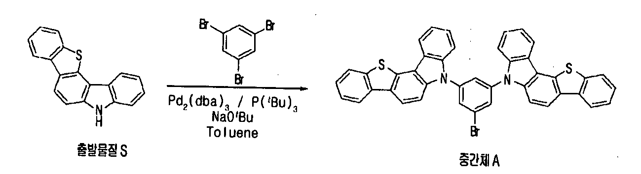
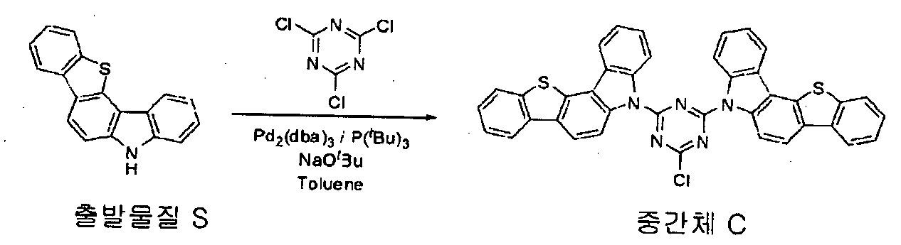
출발물질 S와 1,3,5-tribromobenzene, Pd2(dba)3, P( t Bu)3 그리고 NaO t Bu를 톨루엔 용매에 녹인 후, 110 에서 24시간동안 교반시켰다. 반응이 종료되면 반응물의 온도를 상온으로 낮추고 생성된 고체를 감압여과 후, 뜨거운 톨루엔 용매를 이용하여 재결정화하여 원하는 중간체 A를 얻어내었다(수율: 69%).Starting materials S, 1,3,5-tribromobenzene, Pd 2 (dba) 3 , P ( t Bu) 3 and NaO t Bu were dissolved in toluene solvent and then stirred at 110 to 24 hours. After the reaction was completed, the temperature of the reactant was lowered to room temperature, and the resulting solid was filtered under reduced pressure, and then recrystallized with hot toluene solvent to obtain the desired intermediate A (yield: 69%).
단계 2) 중간체 B의 합성Step 2) Synthesis of Intermediate B
[반응식 2] Scheme 2
[규칙 제91조에 의한 정정 28.04.2011]

[Revisions under Rule 91 28.04.2011]
단계 1)에서 얻은 중간체 A를 무수 THF에 녹이고, 반응물의 온도를 8 로 낮추고, n-BuLi (1.6 M in hexane)을 천천히 적가하고 난 후, 반응물을 0 에서 1시간동안 교반시켰다. 반응물의 온도를 -78 로 낮추고, Isopropoxy-4,4,5,5-tetramethyl-1,3,2-dioxaborolane을 적가하고, 상온에서 12시간동안 교반시켰다. 반응이 종결되면 CH2Cl2로 추출하고 무수 MgSO4로 반응물 내의 물을 제거하고 감압 여과 후, 유기용매를 농축하여 생성된 생성물을 메틸알콜(Methyl alcohol)을The intermediate A obtained in step 1) was dissolved in anhydrous THF, the temperature of the reaction was lowered to 8, n-BuLi (1.6 M in hexane) was slowly added dropwise, and the reaction was stirred at 0 to 1 hour. The temperature of the reaction was lowered to -78, Isopropoxy-4,4,5,5-tetramethyl-1,3,2-dioxaborolane was added dropwise and stirred at room temperature for 12 hours. After completion of the reaction, the mixture was extracted with CH 2 Cl 2 , water was removed from the reaction with anhydrous MgSO 4 , filtered under reduced pressure, and the organic solvent was concentrated to give the resulting product as methyl alcohol.
사용하여 재결정화하여 원하는 중간체 B를 얻었다(수율: 62%).Recrystallization was used to afford the desired intermediate B (yield: 62%).
단계 3) 중간체 C의 합성Step 3) Synthesis of Intermediate C
[반응식 3] Scheme 3
[규칙 제91조에 의한 정정 28.04.2011]
[Revisions under Rule 91 28.04.2011]
출발물질 S와 Cyanuric chloride, Pd2(dba)3, P( t Bu)3 그리고 NaO t Bu를 톨루엔 용매에 녹인 후, 110 에서 24시간동안 교반시켰다. 반응이 종료되면 반응물의 온도를 상온으로 낮추고 생성된 고체를 감압여과 후, 뜨거운 톨루엔 용매를 이용하여 재결정화하여 원하는 중간체 C를 얻어내었다 (수율: 49%).Starting materials S, Cyanuric chloride, Pd 2 (dba) 3 , P ( t Bu) 3 and NaO t Bu were dissolved in toluene solvent and stirred at 110 to 24 hours. After the reaction was completed, the temperature of the reactant was lowered to room temperature, and the resulting solid was filtered under reduced pressure, and then recrystallized with hot toluene solvent to obtain the desired intermediate C (yield: 49%).
합성예1: 화합물 10의 합성Synthesis Example 1 Synthesis of Compound 10
[반응식 4] Scheme 4
[규칙 제91조에 의한 정정 28.04.2011]

[Revisions under Rule 91 28.04.2011]
단계 1)에서 합성한 중간체 A와 9-Anthraceneboronic acid, Pd(PPh3)4 그리고 K2CO3를 무수 THF와 소량의 물에 녹인 후, 24시간동안 환류시켰다. 반응이 종료되면 반응물의 온도를 상온으로 식힘 다음 CH2Cl2로 추출하고 물로 닦아주었다. 무수 MgSO4로 소량의 물을 제거하고 감압여과 후, 유기 용매를 농축하여 생성된 생성물을 톨루엔 용매를 이용하여 재결정화하여 원하는 화합물 10을 얻어내었다 (수율: 71%).The intermediate A, 9-Anthraceneboronic acid, Pd (PPh 3 ) 4 and K 2 CO 3 synthesized in step 1) were dissolved in anhydrous THF and a small amount of water, and then refluxed for 24 hours. After the reaction was completed, the reaction was cooled to room temperature, extracted with CH 2 Cl 2 , and washed with water. After removal of a small amount of water with anhydrous MgSO 4 and filtration under reduced pressure, the organic solvent was concentrated and the resulting product was recrystallized using a toluene solvent to give the desired compound 10 (yield: 71%).
합성예 2: 화합물 26의 합성Synthesis Example 2 Synthesis of Compound 26
[반응식 5] Scheme 5
[규칙 제91조에 의한 정정 28.04.2011]
[Revisions under Rule 91 28.04.2011]
단계 2)에서 합성한 중간체 B와 2-Iodo-4,6-diphenylpyrimidine, Pd(PPh3)4 그리고 K2CO3를 무수 THF와 소량의 물에 녹인 후, 24시간동안 환류시켰다. 반응이 종료되면 반응물의 온도를 상온으로 식힘 다음 CH2Cl2로 추출하고 물로 닦아주었다. 무수 MgSO4로 소량의 물을 제거하고 감압여과 후, 유기 용매를 농축하여 생성된 생성물을 톨루엔 용매를 이용하여 재결정화하여 원하는 화합물 26을 얻어내었다 (수율: 54%).The intermediate B, 2-Iodo-4,6-diphenylpyrimidine, Pd (PPh 3 ) 4 and K 2 CO 3 synthesized in step 2) were dissolved in anhydrous THF and a small amount of water, and then refluxed for 24 hours. After the reaction was completed, the reaction was cooled to room temperature, extracted with CH 2 Cl 2 , and washed with water. After removal of a small amount of water with anhydrous MgSO 4 and filtration under reduced pressure, the organic solvent was concentrated and the resulting product was recrystallized using a toluene solvent to give the desired compound 26 (yield: 54%).
합성예 3: 화합물 38의 합성Synthesis Example 3 Synthesis of Compound 38
[반응식 6] Scheme 6
[규칙 제91조에 의한 정정 28.04.2011]

[Revisions under Rule 91 28.04.2011]
단계 3)에서 합성한 중간체 C와 2-Naphthylboronic acid, Pd(PPh3)4 그리고 K2CO3를 무수 THF와 소량의 물에 녹인 후, 24시간동안 환류시켰다. 반응이 종료되면 반응물의 온도를 상온으로 식힘 다음 CH2Cl2로 추출하고 물로 닦아주었다. 무수 MgSO4로 소량의 물을 제거하고 감압여과 후, 유기 용매를 농축하여 생성된 생성물을 톨루엔 용매를 이용하여 재결정화하여 원하는 화합물 38을 얻어내었다 (수율: 77%).Intermediate C, 2-Naphthylboronic acid, Pd (PPh 3 ) 4 and K 2 CO 3 synthesized in step 3) were dissolved in anhydrous THF and a small amount of water, and then refluxed for 24 hours. After the reaction was completed, the reaction was cooled to room temperature, extracted with CH 2 Cl 2 , and washed with water. After removal of a small amount of water with anhydrous MgSO 4 and filtration under reduced pressure, the organic solvent was concentrated and the resulting product was recrystallized using a toluene solvent to give the desired compound 38 (yield: 77%).
합성예 4: 화합물 56의 합성Synthesis Example 4 Synthesis of Compound 56
[반응식 7] Scheme 7
[규칙 제91조에 의한 정정 28.04.2011]
[Revisions under Rule 91 28.04.2011]
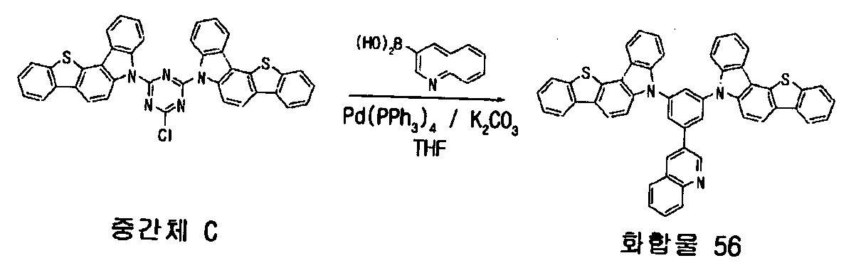
단계 3)에서 합성한 중간체 C와 Quinolin-3-ylboronic acid, Pd(PPh3)4 그리고 K2CO3를 무수 THF와 소량의 물에 녹인 후, 24시간동안 환류시켰다. 반응이 종료되면 반응물의 온도를 상온으로 식힘 다음 CH2Cl2로 추출하고 물로 닦아주었다. 무수 MgSO4로 소량의 물을 제거하고 감압여과 후, 유기 용매를 농축하여 생성된 생성물을 톨루엔 용매를 이용하여 재결정화하여 원하는 화합물 56을 얻어내었다 (수율: 65%).Intermediate C, Quinolin-3-ylboronic acid, Pd (PPh 3 ) 4 and K 2 CO 3 synthesized in step 3) were dissolved in anhydrous THF and a small amount of water, and then refluxed for 24 hours. After the reaction was completed, the reaction was cooled to room temperature, extracted with CH 2 Cl 2 , and washed with water. After removal of a small amount of water with anhydrous MgSO 4 and filtration under reduced pressure, the organic solvent was concentrated and the resulting product was recrystallized using a toluene solvent to give the desired compound 56 (yield: 65%).
이때 화학식1 내지 3으로 표시되는 화합물들은 R1, R2, R3, R4, R5, R6, R7, R8, R9, R10, R1', R2', R3', R4 ', R5', R6', R7', R8', R9', 및 R10' 의 치환기들의 치환 또는 비치환된 치환기들은 광범위한 관계로 화학식 4로 표시한 화합물들 중 일부의 합성예를 예시적으로 설명하였으나 합성예로 예시적으로 설명하지 않은 화학식 1 내지 4로 표시되는 화합물들도 본 명세서의 일부를 구성할 수 있다.In this case, the compounds represented by Formulas 1 to 3 are R 1 , R 2 , R 3 , R 4 , R 5 , R 6 , R 7 , R 8 , R 9 , R 10 , R 1 ', R 2 ', R 3 Substituted or unsubstituted substituents of the substituents of ', R 4 ', R 5 ', R 6 ', R 7 ', R 8 ', R 9 ', and R 10 ' are compounds represented by the general formula (4) in a broad relationship. Synthesis examples of some of the above, but the compounds represented by the formula (1) to 4 not illustratively described as a synthesis example may also form part of the present specification.
유기 전계 소자의 제조 평가Manufacturing Evaluation of Organic Field Devices
합성을 통해 얻은 화합물들 10, 26, 38, 56 각각을 발광층의 발광 호스트 물질로 사용하여 통상적인 방법에 따라 유기전계 발광소자를 제작하였다. Compounds 10, 26, 38, and 56 obtained through synthesis were used as light emitting host materials of the light emitting layer, respectively, to fabricate an organic light emitting diode according to a conventional method.
먼저, 유리 기판에 형성된 ITO층(양극) 위에 우선 홀 주입층으로서 구리프탈로사이아닌(이하 CuPc로 약기함)막을 진공증착하여 10 nm 두께로 형성하였다. 이어서, 이 막 상에 전공수송 화합물로서 4,4-비스[N-(1-나프틸)-N-페닐아미노]비페닐 (이하 a-NPD로 약기함)을 30 nm의 두께로 진공증착하여 홀 수송층을 형성하였다.First, a copper phthalocyanine (hereinafter abbreviated as CuPc) film was vacuum-deposited on the ITO layer (anode) formed on the glass substrate to form a thickness of 10 nm. Subsequently, 4,4-bis [N- (1-naphthyl) -N-phenylamino] biphenyl (hereinafter abbreviated as a-NPD) was vacuum-deposited on the membrane as a major transport compound. A hole transport layer was formed.
홀 수송층을 형성한 후, 이 홀 수송층 상부에 화합물들 10, 26, 38, 56 각각을 인광 호스트 재료로서 증착하여 발광층을 성막하였다. After the hole transport layer was formed, compounds 10, 26, 38, and 56 were deposited on the hole transport layer as phosphorescent host materials to form a light emitting layer.
동시에 인광 발광성의 Ir 금속착체 도펀트로서 트리스(2-페닐피리딘)이리듐 (이하 I r(ppy)3로 약기함)을 첨가하였다. 이때 발광층 중에 있어서의 I r(ppy)3의 농도는 5중량%로 하였다. 홀 저지층으로 (1,1-비스페닐)-4-올레이토)비스(2-메틸-8-퀴놀린올레이토)알루미늄 (이하 BAlq로 약기함)을 10 nm 의 두께로 진공증착하고, 이어서 전자주입층으로 트리스(8-퀴놀리놀)알루미늄 (이하 Alq3로 약칭함)을 40 nm의 두께로 성막하였다. 이 후, 할로젠화 알칼리 금속인 LiF를 0.2 nm의 두께로 증착하고, 이어서 Al을 150 nm의 두께로 증착하여 이 Al/LiF를 음극으로 사용함으로서 유기전계 발광소자를 제조하였다.At the same time, tris (2-phenylpyridine) iridium (abbreviated as I r (ppy) 3 hereinafter) was added as a phosphorescent Ir metal complex dopant. At this time, the concentration of I r (ppy) 3 in the light emitting layer was 5% by weight. (1,1-bisphenyl) -4-oleato) bis (2-methyl-8-quinolinoleito) aluminum (hereinafter abbreviated as BAlq) was vacuum-deposited to a thickness of 10 nm as a hole blocking layer, followed by electrons. Tris (8-quinolinol) aluminum (hereinafter abbreviated to Alq 3 ) was formed into an injection layer to a thickness of 40 nm. Thereafter, LiF, an alkali metal halide, was deposited to a thickness of 0.2 nm, and then Al was deposited to a thickness of 150 nm to use an Al / LiF as a cathode to prepare an organic light emitting device.
비교실험예1Comparative Example 1
비교를 위해, 본 발명의 화합물 대신에 화학식 13로 표시되는 화합물(이하 CBP로 약기함)을 발광 호스트 물질로 사용하여 시험예와 동일한 구조의 유기전계발광소자를 제작하였다. For comparison, an organic electroluminescent device having the same structure as the test example was manufactured using a compound represented by Chemical Formula 13 (hereinafter abbreviated as CBP) as a light emitting host material instead of the compound of the present invention.
[화학식 5][Formula 5]

표 1
Table 1
| 발광층의호스트 재료 | 전압( V ) | 전류밀도( mA/cm2 ) | 휘도( cd/m2 ) | 발광효율( cd/A ) | 색도좌표( x, y ) | |
| 실시예 1 | 화합물 10 | 5.1 | 0.31 | 107 | 62.3 | (0.30, 0.60) |
| 실시예 2 | 화합물 26 | 4.9 | 0.30 | 105 | 68.2 | (0.32, 0.61) |
| 실시예 3 | 화합물 38 | 5.2 | 0.33 | 107 | 58.3 | (0.30, 0.60) |
| 실시예 4 | 화합물 56 | 5.0 | 0.32 | 107 | 65.3 | (0.30, 0.60) |
| 비교예 1 | CBP | 6.1 | 0.31 | 101 | 32.6 | (0.33, 0.61) |
| Host material of emitting layer | Voltage (V) | Current density (mA / cm 2 ) | Luminance (cd / m 2 ) | Luminous Efficiency (cd / A) | Chromaticity coordinates (x, y) | |
| Example 1 | Compound 10 | 5.1 | 0.31 | 107 | 62.3 | (0.30, 0.60) |
| Example 2 | Compound 26 | 4.9 | 0.30 | 105 | 68.2 | (0.32, 0.61) |
| Example 3 | Compound 38 | 5.2 | 0.33 | 107 | 58.3 | (0.30, 0.60) |
| Example 4 | Compound 56 | 5.0 | 0.32 | 107 | 65.3 | (0.30, 0.60) |
| Comparative Example 1 | CBP | 6.1 | 0.31 | 101 | 32.6 | (0.33, 0.61) |
상기 표 1의 결과로부터 알 수 있듯이, 상기 표의 결과로부터 알 수 있듯이, 본 발명의 유기전계발광소자용 재료를 이용한 유기전계발광소자는 발광효율이 비교예로 사용된 CBP에 비해 월등히 우수할 뿐만 아니라 색순도가 현저히 개선된 녹색 발광이 얻어지므로 유기전계발광 소자의 인광 호스트 물질로 사용되어 발광효율 및 색순도를 현저히 개선시킬 수 있다.As can be seen from the results of Table 1, as can be seen from the results of the table, the organic electroluminescent device using the organic electroluminescent device material of the present invention is not only excellent in the luminous efficiency compared to the CBP used as a comparative example, Since green light emission is obtained in which color purity is remarkably improved, it is used as a phosphorescent host material of an organic light emitting display device, and thus light emission efficiency and color purity may be remarkably improved.
본 발명의 화합물들을 유기전계발광소자의 다른 유기물층들, 예를 들어 발광층의 호스트 재료 뿐만 아니라, 전자주입층, 전자수송층, 정공주입층 및 정공수송층에 사용되더라도 동일한 효과를 얻을 수 있는 것은 자명하다.It is apparent that the same effect can be obtained even when the compounds of the present invention are used in other organic material layers of the organic light emitting device, for example, the host material of the light emitting layer, as well as the electron injection layer, the electron transport layer, the hole injection layer and the hole transport layer.
이때 화학식1 내지 4로 표시되는 화합물들은 R1, R2, R3, R4, R5, R6, R7, R8, R9, R10, R1', R2', R3', R4 ', R5', R6', R7', R8', R9', 및 R10' 의 치환 또는 비치환된 치환기들은 광범위한 관계로 화학식 4으로 표시한 화합물들 중 일부의 비교실시예를 예시적으로 설명하였으나 비교실시예로 예시적으로 설명하지 않은 화학식 1 내지 3로 표시되는 화합물들도 전술한 화학식 1 내지 3의 모핵 구조를 가지는 이유로 전술한 비교실시예들과 동일한 효과를 나타내는 것으로 확인할 수 있으며 그 결과는 본 명세서의 일부를 구성할 수 있다.In this case, the compounds represented by Formulas 1 to 4 are R 1 , R 2 , R 3 , R 4 , R 5 , R 6 , R 7 , R 8 , R 9 , R 10 , R 1 ', R 2 ', R 3 Substituted or unsubstituted substituents of ', R 4 ', R 5 ', R 6 ', R 7 ', R 8 ', R 9 ', and R 10 ' are some of the compounds represented by the formula (4) in a broad relationship. Compounds represented by the formulas (1) to (3), which have been described by way of example but not described by way of example, are also the same as the aforementioned comparative examples because of the above-described parent nucleus structure of the formulas (1) to (3). It can be confirmed that the effect and the results may form part of the present specification.
이상의 설명은 본 발명을 예시적으로 설명한 것에 불과한 것으로, 본 발명이 속하는 기술분야에서 통상의 지식을 가지는 자라면 본 발명의 본질적인 특성에서 벗어나지 않는 범위에서 다양한 변형이 가능할 것이다. 따라서, 본 명세서에 개시된 실시예들은 본 발명을 한정하기 위한 것이 아니라 설명하기 위한 것이고, 이러한 실시예에 의하여 본 발명의 사상과 범위가 한정되는 것은 아니다.The above description is merely illustrative of the present invention, and those skilled in the art to which the present invention pertains may various modifications without departing from the essential characteristics of the present invention. Accordingly, the embodiments disclosed herein are not intended to limit the present invention but to describe the present invention, and the spirit and scope of the present invention are not limited by these embodiments.
본 발명의 보호범위는 아래의 청구범위에 의하여 해석되어야 하며, 그와 동등한 범위 내에 있는 모든 기술은 본 발명의 권리범위에 포함되는 것으로 해석되어야 할 것이다.The protection scope of the present invention should be interpreted by the following claims, and all the technologies within the equivalent scope should be interpreted as being included in the scope of the present invention.
CROSS-REFERENCE TO RELATED APPLICATIONCROSS-REFERENCE TO RELATED APPLICATION
본 특허출원은 2010년 3월 5일 한국에 출원한 특허출원번호 제 10-2010-This patent application is filed in Korea on March 5, 2010. Patent Application No. 10-2010-
0019950 호에 대해 미국 특허법 119(a)조(35 U.S.C § 119(a))에 따라 우선권을 주장하며, 그 모든 내용은 참고문헌으로 본 특허출원에 병합된다. 아울러, 본 특허출원은 미국 이외에 국가에 대해서도 위와 동일한 동일한 이유로 우선권을 주장하면 그 모든 내용은 참고문헌으로 본 특허출원에 병합된다. 0019950 claims priority under U.S. Patent Act Article 119 (a) (35 U.S.C § 119 (a)), all of which is incorporated herein by reference. In addition, if this patent application claims priority for the same reason as above for a country other than the United States, all the contents thereof are incorporated into this patent application by reference.
Claims (11)
- 다음 화학식으로 표시되는 화합물.A compound represented by the following formula.
 위 화학식에 있어서, In the above formula,(1) R1, R2, R3, R4, R5, R6, R7, R8, R9, R10, R1', R2', R3', R4 ', R5', R6', R7', R8', R9', 및 R10'은 각각 서로 독립적으로 수소 원자, 할로겐 원자, 시아노기, 알콕시기, 티올기, 치환 또는 비치환된 탄소수 1 내지 50의 알킬기, 치환 또는 비치환된 탄소수 1 내지 50의 알콕시기, 치환 또는 비치환의 탄소수 1 내지 50의 알케닐기, 치환 또는 비치환의 탄소수 5 내지 60의 아릴렌기, 치환 또는 비치환된 탄소수 5 내지 60의 아릴기, 치환 또는 비치환된 탄소수 5 내지 60의 아릴옥시기, 황(S), 질소(N), 산소(O), 인(P) 및 규소(Si)를 적어도 하나 이상 포함하는 치환 또는 비치환된 탄소수 1 내지 50의 알킬기 또는 황(S), 질소(N), 산소(O), 인(P) 및 규소(Si)를 적어도 하나 이상 포함하는 치환 또는 비치환된 탄소수 5 내지 60의 헤테로아릴기 또는 황(S), 질소(N), 산소(O), 인(P) 및 규소(Si)를 적어도 하나 이상 포함하는 치환 또는 비치환된 탄소수 5 내지 60의 헤테로아릴옥시기이며, (1) R 1 , R 2 , R 3 , R 4 , R 5 , R 6 , R 7 , R 8 , R 9 , R 10 , R 1 ', R 2 ', R 3 ', R 4 ', R 5 ′, R 6 ′, R 7 ′, R 8 ′, R 9 ′, and R 10 ′ each independently represent a hydrogen atom, a halogen atom, a cyano group, an alkoxy group, a thiol group, a substituted or unsubstituted carbon number 1 An alkyl group of 50 to 50, a substituted or unsubstituted alkoxy group of 1 to 50 carbon atoms, a substituted or unsubstituted alkenyl group of 1 to 50 carbon atoms, a substituted or unsubstituted arylene group of 5 to 60 carbon atoms, a substituted or unsubstituted carbon number 5 to Substitutes containing at least one aryl group of 60, a substituted or unsubstituted aryloxy group having 5 to 60 carbon atoms, sulfur (S), nitrogen (N), oxygen (O), phosphorus (P) and silicon (Si) Or a substituted or unsubstituted C 5 to 60 carbon atoms containing at least one unsubstituted alkyl group having 1 to 50 carbon atoms or sulfur (S), nitrogen (N), oxygen (O), phosphorus (P) and silicon (Si). Heteroaryl group or sulfur (S), nitrogen (N), oxygen (O), (P) and a silicon (Si) substituted or unsubstituted hetero aryloxy group having 5 to 60 ring containing at least one,(2) X는 탄소(C) 또는 질소(N)이며, (2) X is carbon (C) or nitrogen (N),(3) Ar은 수소 원자, 할로겐 원자, 시아노기, 알콕시기, 티올기, 치환 또는 비치환된 탄소수 1 내지 50의 알킬기, 치환 또는 비치환의 탄소수 1 내지 50의 알케닐기, 치환 또는 비치환의 탄소수 5 내지 60의 아릴렌기, 치환 또는 비치환된 탄소수 5 내지 60의 아릴기, 치환 또는 비치환된 탄소수 5 내지 60의 아릴옥시기, 황(S), 질소(N), 산소(O), 인(P) 및 규소(Si)를 적어도 하나 이상 포함하는 치환 또는 비치환된 탄소수 1 내지 50의 알킬기 또는 황(S), 질소(N), 산소(O), 인(P) 및 규소(Si)를 적어도 하나 이상 포함하는 치환 또는 비치환된 탄소수 5 내지 60의(3) Ar is a hydrogen atom, a halogen atom, a cyano group, an alkoxy group, a thiol group, a substituted or unsubstituted alkyl group having 1 to 50 carbon atoms, a substituted or unsubstituted alkenyl group having 1 to 50 carbon atoms, a substituted or unsubstituted carbon number 5 To 60 arylene group, substituted or unsubstituted aryl group having 5 to 60 carbon atoms, substituted or unsubstituted aryloxy group having 5 to 60 carbon atoms, sulfur (S), nitrogen (N), oxygen (O), phosphorus ( A substituted or unsubstituted alkyl group having 1 to 50 carbon atoms or at least one of P) and silicon (Si) or sulfur (S), nitrogen (N), oxygen (O), phosphorus (P) and silicon (Si); Substituted or unsubstituted C 5 to 60 containing at least one or more헤테로아릴기 또는 황(S), 질소(N), 산소(O), 인(P) 및 규소(Si)를 적어도 하나 이상 포함하는 치환 또는 비치환된 탄소수 5 내지 60의 헤테로아릴옥시기이다.Heteroaryl group or substituted or unsubstituted heteroaryloxy group having 5 to 60 carbon atoms containing at least one or more sulfur (S), nitrogen (N), oxygen (O), phosphorus (P) and silicon (Si).
 - [규칙 제91조에 의한 정정 28.04.2011]
제1항에 있어서, 상기 화합물은 다음 화학식으로 표시되는 화합물인 것을 특징으로 하는 화합물.[Revisions under Rule 91 28.04.2011]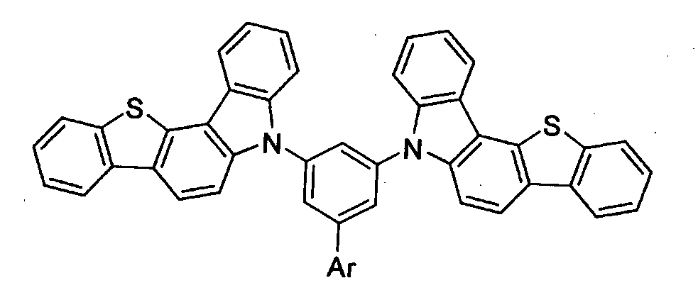
The compound according to claim 1, wherein the compound is a compound represented by the following formula. - [규칙 제91조에 의한 정정 28.04.2011]
제1항에 있어서, 상기 화합물은 다음 화학식으로 표시되는 화합물인 것을 특징으로 하는 화합물.[Revisions under Rule 91 28.04.2011]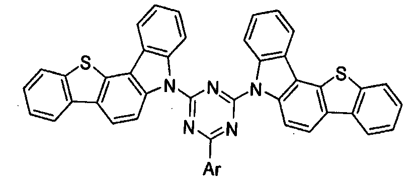
The compound according to claim 1, wherein the compound is a compound represented by the following formula. - 제1항에 있어서,The method of claim 1,상기 R1 내지 R10 및 R1' 내지 R10'은 인접한 기와 결합하여 포화 또는 불포화 고리를 형성하는 것을 특징으로 하는 화합물.R 1 to R 10 and R 1 ′ to R 10 ′ combine with adjacent groups to form a saturated or unsaturated ring.
- [규칙 제91조에 의한 정정 28.04.2011]
제1항에 있어서,상기 화합물은,


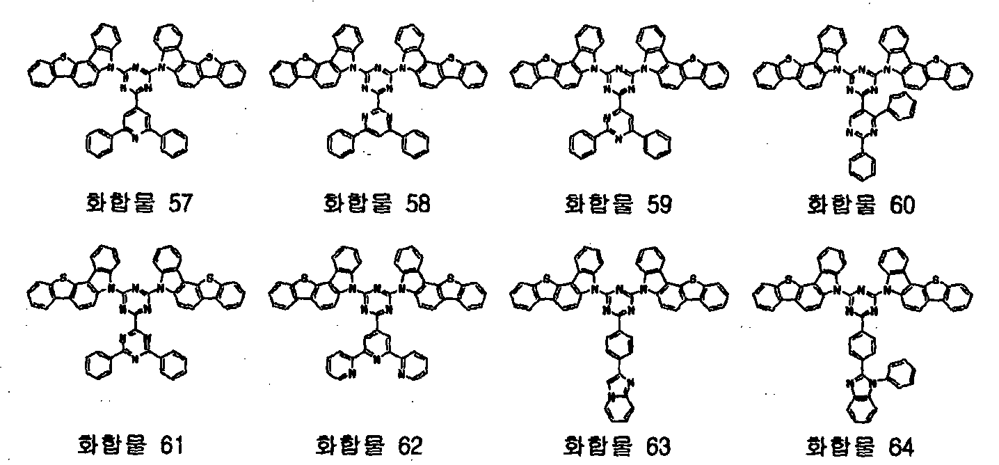 으로 구성된 그룹에서 선택된 하나인 것을 특징으로 하는 화합물.[Revisions under Rule 91 28.04.2011]
The method of claim 1,The compound is,Compounds, characterized in that one selected from the group consisting of. - 제1항 내지 제5항 중 하나의 화합물을 포함하는 1층 이상의 유기물층을 포함하는 유기전기소자.An organic electric device comprising at least one organic material layer comprising a compound of any one of claims 1 to 5.
- 제6항에 있어서,The method of claim 6,상기 화합물을 용액 공정(soluble process)에 의해 상기 유기물층을 형성하는 것을 특징으로 하는 유기전기소자.The organic electroluminescent device according to claim 1, wherein the organic layer is formed by a solution process.
- 제6항에 있어서,The method of claim 6,상기 유기전기소자는 제1 전극, 상기 1층 이상의 유기물층 및 제2 전극을 순차적으로 적층된 형태로 포함하는 유기전계발광소자인 것을 특징으로 하는 유기전기소자.The organic electroluminescent device is an organic electroluminescent device comprising a first electrode, the at least one organic material layer and the second electrode in a stacked form sequentially.
- 제8항에 있어서,The method of claim 8,상기 유기물층은 발광층을 포함하며,The organic material layer includes a light emitting layer,상기 발광층에서 상기 화합물이 호스트 물질로 사용되는 것을 특징으로 하는 유기전기소자.The organic electroluminescent device according to claim 1, wherein the compound is used as a host material in the emission layer.
- 제6항의 유기전기소자를 포함하는 디스플레이장치와;A display device comprising the organic electric element of claim 6;상기 디스플레이장치를 구동하는 제어부를 포함하는 단말.And a control unit for driving the display device.
- 제10항에 있어서,The method of claim 10,상기 유기전기소자는 유기전계발광소자(OLED), 유기태양전지, 유기감광체(OPC) 드럼, 유기트랜지스트(유기 TFT), 포토다이오드(photodiode), 유기레이저(organic laser), 레이저 다이오드(laser diode) 중 하나인 것을 특징으로 하는 단말.The organic electroluminescent device includes an organic light emitting diode (OLED), an organic solar cell, an organic photoconductor (OPC) drum, an organic transistor (organic TFT), a photodiode, an organic laser, and a laser diode. Terminal) characterized in that one of.
Applications Claiming Priority (2)
| Application Number | Priority Date | Filing Date | Title |
|---|---|---|---|
| KR10-2010-0019950 | 2010-03-05 | ||
| KR1020100019950A KR101181280B1 (en) | 2010-03-05 | 2010-03-05 | Compound Containing 5-Membered Heterocycle And Organic Electronic Element Using The Same, Terminal Thereof |
Publications (3)
| Publication Number | Publication Date |
|---|---|
| WO2011108902A2 WO2011108902A2 (en) | 2011-09-09 |
| WO2011108902A3 WO2011108902A3 (en) | 2012-01-12 |
| WO2011108902A9 true WO2011108902A9 (en) | 2012-03-01 |
Family
ID=44542753
Family Applications (1)
| Application Number | Title | Priority Date | Filing Date |
|---|---|---|---|
| PCT/KR2011/001539 WO2011108902A2 (en) | 2010-03-05 | 2011-03-07 | Compound comprising at least two compounds comprising at least two five-membered hetero rings, an organic electrical element using the same and a terminal thereof |
Country Status (2)
| Country | Link |
|---|---|
| KR (1) | KR101181280B1 (en) |
| WO (1) | WO2011108902A2 (en) |
Families Citing this family (24)
| Publication number | Priority date | Publication date | Assignee | Title |
|---|---|---|---|---|
| DE102010054316A1 (en) | 2010-12-13 | 2012-06-14 | Merck Patent Gmbh | Substituted tetraarylbenzenes |
| KR20120078326A (en) * | 2010-12-31 | 2012-07-10 | 제일모직주식회사 | Compound for organic photoelectric device and organic photoelectric device including the same |
| KR101887003B1 (en) * | 2011-07-21 | 2018-08-13 | 롬엔드하스전자재료코리아유한회사 | Novel organic electroluminescence compounds and organic electroluminescence device using the same |
| KR20130011405A (en) * | 2011-07-21 | 2013-01-30 | 롬엔드하스전자재료코리아유한회사 | Novel organic electroluminescence compounds and organic electroluminescence device using the same |
| US9353085B2 (en) * | 2011-08-26 | 2016-05-31 | E-Ray Optoelectronics Technology Co., Ltd. | Compound for organic electroluminescent device and organic electroluminescent devices using the same |
| JP5868652B2 (en) * | 2011-10-18 | 2016-02-24 | 出光興産株式会社 | Aromatic amine derivative and organic electroluminescence device using the same |
| WO2013069939A1 (en) * | 2011-11-07 | 2013-05-16 | 덕산하이메탈(주) | Compound for organic electronic element, organic electronic element including the same, electronic device thereof |
| KR101497133B1 (en) | 2011-12-23 | 2015-02-27 | 제일모직 주식회사 | Compound for organic OPTOELECTRONIC device, ORGANIC LIGHT EMITTING DIODE INCLUDING THE SAME and DISPLAY INCLUDING THE organic LIGHT EMITTING DIODE |
| KR20130084093A (en) * | 2012-01-16 | 2013-07-24 | 롬엔드하스전자재료코리아유한회사 | Novel organic electroluminescence compounds and organic electroluminescence device using the same |
| KR20130094903A (en) * | 2012-02-17 | 2013-08-27 | 롬엔드하스전자재료코리아유한회사 | Novel organic electroluminescent compounds |
| KR20130127563A (en) * | 2012-05-02 | 2013-11-25 | 롬엔드하스전자재료코리아유한회사 | Novel organic electroluminescence compounds and organic electroluminescence device containing the same |
| KR101488560B1 (en) * | 2012-05-08 | 2015-02-03 | 주식회사 두산 | Novel compounds and organic electro luminescence device using the same |
| KR20140049181A (en) * | 2012-10-16 | 2014-04-25 | 롬엔드하스전자재료코리아유한회사 | Organic electroluminescence compounds and organic electroluminescence device comprising the same |
| EP2933852B2 (en) | 2014-04-17 | 2023-09-06 | Novaled GmbH | Phosphorescent OLED and hole transporting materials for phosphorescent OLEDs |
| WO2015190400A1 (en) * | 2014-06-11 | 2015-12-17 | 保土谷化学工業株式会社 | Pyrimidine derivative and organic electroluminescent element |
| US10418562B2 (en) | 2015-02-06 | 2019-09-17 | Universal Display Corporation | Organic electroluminescent materials and devices |
| WO2016129687A1 (en) * | 2015-02-13 | 2016-08-18 | 出光興産株式会社 | Compound, composition, organic electroluminescent element, and electronic device |
| KR101965928B1 (en) * | 2015-06-29 | 2019-04-04 | 주식회사 두산 | Organic light-emitting compound and organic electroluminescent device using the same |
| KR102587382B1 (en) * | 2016-04-29 | 2023-10-12 | 솔루스첨단소재 주식회사 | Organic light-emitting compound and organic electroluminescent device using the same |
| CN106892901A (en) * | 2017-04-21 | 2017-06-27 | 瑞声光电科技(常州)有限公司 | Triaizine compounds and luminescent device |
| DE102017112435B4 (en) * | 2017-06-06 | 2019-01-17 | Cynora Gmbh | Organic molecules, in particular for use in optoelectronic devices |
| WO2019190248A1 (en) * | 2018-03-28 | 2019-10-03 | 주식회사 엘지화학 | Compound and organic light emitting diode comprising same |
| KR20240085849A (en) | 2022-12-08 | 2024-06-17 | 듀폰스페셜티머터리얼스코리아 유한회사 | Compound and organic electroluminescent device comprising the same |
| CN116082328A (en) * | 2023-01-13 | 2023-05-09 | 长春海谱润斯科技股份有限公司 | Imidazole compound and organic electroluminescent device thereof |
Family Cites Families (4)
| Publication number | Priority date | Publication date | Assignee | Title |
|---|---|---|---|---|
| KR101146976B1 (en) * | 2005-01-06 | 2012-05-23 | 삼성모바일디스플레이주식회사 | Blue electroluminescent polymer and organoelectroluminescent device employing the same |
| US20080166594A1 (en) | 2005-06-24 | 2008-07-10 | Idemitsu Kosan Co., Ltd. | Benzothiophene derivative and organic electroluminescence device making use of the same |
| JP4867244B2 (en) | 2005-09-12 | 2012-02-01 | Jsr株式会社 | Charge transporting compound and method for producing the same, composition for organic electroluminescence device, and organic electroluminescence device |
| JP5049711B2 (en) | 2006-09-27 | 2012-10-17 | 富士フイルム株式会社 | Organic electroluminescence device |
-
2010
- 2010-03-05 KR KR1020100019950A patent/KR101181280B1/en active IP Right Grant
-
2011
- 2011-03-07 WO PCT/KR2011/001539 patent/WO2011108902A2/en active Application Filing
Also Published As
| Publication number | Publication date |
|---|---|
| KR20110100877A (en) | 2011-09-15 |
| WO2011108902A3 (en) | 2012-01-12 |
| KR101181280B1 (en) | 2012-09-10 |
| WO2011108902A2 (en) | 2011-09-09 |
Similar Documents
| Publication | Publication Date | Title |
|---|---|---|
| WO2011108902A9 (en) | Compound comprising at least two compounds comprising at least two five-membered hetero rings, an organic electrical element using the same and a terminal thereof | |
| WO2011019173A2 (en) | Compound containing 5-membered heterocycles, organic light-emitting device using same, and terminal comprising the latter | |
| WO2010131855A2 (en) | Compound containing a 5-membered heterocycle and organic light-emitting diode using same, and terminal for same | |
| WO2010114267A2 (en) | Organic electronic device, compounds for same, and terminal | |
| KR101219492B1 (en) | Compound Containing 5-Membered Heterocycle And Organic Electronic Element Using The Same, Terminal Thereof | |
| WO2011021803A2 (en) | Compound having a thianthrene structure, organic light-emitting device using same, and terminal comprising the device | |
| WO2011155742A2 (en) | Compound comprising carbazole and aromatic amine derivatives, organic electronic element using same, and terminal comprising the organic electronic element | |
| KR101245243B1 (en) | Spiro Carbazole Compound And Organic Electronic Element Using The Same, Terminal Thereof | |
| KR101144358B1 (en) | Compound Containing 5-Membered Heterocycle And Organic Electronic Element Using The Same, Terminal Thereof | |
| WO2012067415A2 (en) | Compound and organic electronic device using same, and terminal comprising the organic electronic device | |
| WO2011102573A1 (en) | Compound including indole derivative, organic electronic element using same, and terminal thereof | |
| KR20110066763A (en) | Compound containing indoloacridine and organic electronic element using the same, terminal thereof | |
| KR20110129766A (en) | Compound containing five membered heterocyclic compound, and organic electronic element using the same, terminal thereof | |
| WO2011149284A2 (en) | Hetero-atom-containing compound in which carbazole and fluorene are fused, an organic electrical element using the same and a terminal thereof | |
| KR20110103141A (en) | Compound containing indoloacridine and organic electronic element using the same, terminal thereof | |
| WO2011111996A9 (en) | Compound including indole derivative in which two tertiary amines are substituted, organic electronic element using same, and terminal thereof | |
| KR101497122B1 (en) | Compound Containing At Least Two 5-Membered Heterocycle And Organic Electronic Element Using The Same, Terminal Thereof | |
| WO2010085087A2 (en) | Novel cycloalkene derivatives and organic electronic devices using the same | |
| KR20110092263A (en) | Compound containing at least two 5-membered heterocycle and organic electronic element using the same, terminal thereof | |
| KR101146929B1 (en) | Compound Containing At Least Two 5-Membered Heterocycle And Organic Electronic Element Using The Same, Terminal Thereof | |
| KR20110133010A (en) | Compound containing 5-membered heterocycle and organic electronic element using the same, terminal thereof | |
| KR20120006000A (en) | Compound containing 5-membered heterocycle and organic electronic element using the same, terminal thereof | |
| KR20110133007A (en) | Compound containing 5-membered heterocycle and organic electronic element using the same, terminal thereof | |
| KR20100125928A (en) | Compound containing at least two 5-membered heterocycle and organic electronic element using the same, terminal thereof | |
| KR20110133008A (en) | Compound containing 5-membered heterocycle and organic electronic element using the same, terminal thereof |
Legal Events
| Date | Code | Title | Description |
|---|---|---|---|
| NENP | Non-entry into the national phase |
Ref country code: DE |
|
| 122 | Ep: pct application non-entry in european phase |
Ref document number: 11750959 Country of ref document: EP Kind code of ref document: A2 |