EP2933852B2 - Phosphorescent OLED and hole transporting materials for phosphorescent OLEDs - Google Patents
Phosphorescent OLED and hole transporting materials for phosphorescent OLEDs Download PDFInfo
- Publication number
- EP2933852B2 EP2933852B2 EP14165200.8A EP14165200A EP2933852B2 EP 2933852 B2 EP2933852 B2 EP 2933852B2 EP 14165200 A EP14165200 A EP 14165200A EP 2933852 B2 EP2933852 B2 EP 2933852B2
- Authority
- EP
- European Patent Office
- Prior art keywords
- mmol
- aryl
- biphenyl
- layer
- mol
- Prior art date
- Legal status (The legal status is an assumption and is not a legal conclusion. Google has not performed a legal analysis and makes no representation as to the accuracy of the status listed.)
- Active
Links
Images


Classifications
-
- H—ELECTRICITY
- H10—SEMICONDUCTOR DEVICES; ELECTRIC SOLID-STATE DEVICES NOT OTHERWISE PROVIDED FOR
- H10K—ORGANIC ELECTRIC SOLID-STATE DEVICES
- H10K85/00—Organic materials used in the body or electrodes of devices covered by this subclass
- H10K85/60—Organic compounds having low molecular weight
- H10K85/615—Polycyclic condensed aromatic hydrocarbons, e.g. anthracene
-
- C—CHEMISTRY; METALLURGY
- C07—ORGANIC CHEMISTRY
- C07C—ACYCLIC OR CARBOCYCLIC COMPOUNDS
- C07C211/00—Compounds containing amino groups bound to a carbon skeleton
- C07C211/43—Compounds containing amino groups bound to a carbon skeleton having amino groups bound to carbon atoms of six-membered aromatic rings of the carbon skeleton
- C07C211/54—Compounds containing amino groups bound to a carbon skeleton having amino groups bound to carbon atoms of six-membered aromatic rings of the carbon skeleton having amino groups bound to two or three six-membered aromatic rings
-
- C—CHEMISTRY; METALLURGY
- C07—ORGANIC CHEMISTRY
- C07C—ACYCLIC OR CARBOCYCLIC COMPOUNDS
- C07C211/00—Compounds containing amino groups bound to a carbon skeleton
- C07C211/43—Compounds containing amino groups bound to a carbon skeleton having amino groups bound to carbon atoms of six-membered aromatic rings of the carbon skeleton
- C07C211/57—Compounds containing amino groups bound to a carbon skeleton having amino groups bound to carbon atoms of six-membered aromatic rings of the carbon skeleton having amino groups bound to carbon atoms of six-membered aromatic rings being part of condensed ring systems of the carbon skeleton
- C07C211/58—Naphthylamines; N-substituted derivatives thereof
-
- H—ELECTRICITY
- H10—SEMICONDUCTOR DEVICES; ELECTRIC SOLID-STATE DEVICES NOT OTHERWISE PROVIDED FOR
- H10K—ORGANIC ELECTRIC SOLID-STATE DEVICES
- H10K50/00—Organic light-emitting devices
- H10K50/10—OLEDs or polymer light-emitting diodes [PLED]
- H10K50/14—Carrier transporting layers
- H10K50/16—Electron transporting layers
-
- H—ELECTRICITY
- H10—SEMICONDUCTOR DEVICES; ELECTRIC SOLID-STATE DEVICES NOT OTHERWISE PROVIDED FOR
- H10K—ORGANIC ELECTRIC SOLID-STATE DEVICES
- H10K50/00—Organic light-emitting devices
- H10K50/10—OLEDs or polymer light-emitting diodes [PLED]
- H10K50/17—Carrier injection layers
-
- H—ELECTRICITY
- H10—SEMICONDUCTOR DEVICES; ELECTRIC SOLID-STATE DEVICES NOT OTHERWISE PROVIDED FOR
- H10K—ORGANIC ELECTRIC SOLID-STATE DEVICES
- H10K50/00—Organic light-emitting devices
- H10K50/10—OLEDs or polymer light-emitting diodes [PLED]
- H10K50/17—Carrier injection layers
- H10K50/171—Electron injection layers
-
- H—ELECTRICITY
- H10—SEMICONDUCTOR DEVICES; ELECTRIC SOLID-STATE DEVICES NOT OTHERWISE PROVIDED FOR
- H10K—ORGANIC ELECTRIC SOLID-STATE DEVICES
- H10K50/00—Organic light-emitting devices
- H10K50/10—OLEDs or polymer light-emitting diodes [PLED]
- H10K50/18—Carrier blocking layers
-
- H—ELECTRICITY
- H10—SEMICONDUCTOR DEVICES; ELECTRIC SOLID-STATE DEVICES NOT OTHERWISE PROVIDED FOR
- H10K—ORGANIC ELECTRIC SOLID-STATE DEVICES
- H10K85/00—Organic materials used in the body or electrodes of devices covered by this subclass
- H10K85/60—Organic compounds having low molecular weight
- H10K85/631—Amine compounds having at least two aryl rest on at least one amine-nitrogen atom, e.g. triphenylamine
- H10K85/633—Amine compounds having at least two aryl rest on at least one amine-nitrogen atom, e.g. triphenylamine comprising polycyclic condensed aromatic hydrocarbons as substituents on the nitrogen atom
-
- C—CHEMISTRY; METALLURGY
- C07—ORGANIC CHEMISTRY
- C07C—ACYCLIC OR CARBOCYCLIC COMPOUNDS
- C07C2603/00—Systems containing at least three condensed rings
- C07C2603/02—Ortho- or ortho- and peri-condensed systems
- C07C2603/04—Ortho- or ortho- and peri-condensed systems containing three rings
- C07C2603/06—Ortho- or ortho- and peri-condensed systems containing three rings containing at least one ring with less than six ring members
- C07C2603/10—Ortho- or ortho- and peri-condensed systems containing three rings containing at least one ring with less than six ring members containing five-membered rings
- C07C2603/12—Ortho- or ortho- and peri-condensed systems containing three rings containing at least one ring with less than six ring members containing five-membered rings only one five-membered ring
- C07C2603/18—Fluorenes; Hydrogenated fluorenes
-
- H—ELECTRICITY
- H10—SEMICONDUCTOR DEVICES; ELECTRIC SOLID-STATE DEVICES NOT OTHERWISE PROVIDED FOR
- H10K—ORGANIC ELECTRIC SOLID-STATE DEVICES
- H10K2101/00—Properties of the organic materials covered by group H10K85/00
- H10K2101/10—Triplet emission
-
- H—ELECTRICITY
- H10—SEMICONDUCTOR DEVICES; ELECTRIC SOLID-STATE DEVICES NOT OTHERWISE PROVIDED FOR
- H10K—ORGANIC ELECTRIC SOLID-STATE DEVICES
- H10K50/00—Organic light-emitting devices
- H10K50/10—OLEDs or polymer light-emitting diodes [PLED]
- H10K50/11—OLEDs or polymer light-emitting diodes [PLED] characterised by the electroluminescent [EL] layers
-
- H—ELECTRICITY
- H10—SEMICONDUCTOR DEVICES; ELECTRIC SOLID-STATE DEVICES NOT OTHERWISE PROVIDED FOR
- H10K—ORGANIC ELECTRIC SOLID-STATE DEVICES
- H10K50/00—Organic light-emitting devices
- H10K50/10—OLEDs or polymer light-emitting diodes [PLED]
- H10K50/14—Carrier transporting layers
- H10K50/15—Hole transporting layers
- H10K50/155—Hole transporting layers comprising dopants
-
- H—ELECTRICITY
- H10—SEMICONDUCTOR DEVICES; ELECTRIC SOLID-STATE DEVICES NOT OTHERWISE PROVIDED FOR
- H10K—ORGANIC ELECTRIC SOLID-STATE DEVICES
- H10K85/00—Organic materials used in the body or electrodes of devices covered by this subclass
- H10K85/60—Organic compounds having low molecular weight
- H10K85/615—Polycyclic condensed aromatic hydrocarbons, e.g. anthracene
- H10K85/626—Polycyclic condensed aromatic hydrocarbons, e.g. anthracene containing more than one polycyclic condensed aromatic rings, e.g. bis-anthracene
Definitions
- the present invention relates to phosphorescent organic light-emitting devices, and to compounds which may be used in such devices, especially in hole transporting and/or electron blocking layers thereof.
- the electroluminescence (EL) property of certain organic materials is used.
- EL devices suitable charge carriers are formed under application of a voltage across the device. Recombination of these charge carriers results in an excited state, which relaxes to the ground state under light emission.
- the organic light-emitting diodes very often have, besides the emission layer, also charge transporting layers which are responsible for transport of negative and positive charge carriers into the emission layer. These charge transporting layers are grouped, depending on the charge carrier transported, into hole conductors and electron conductors. A quite similar set of layers is known for photovoltaic devices, such as organic solar cells.
- Organic semiconducting devices having several layers are produced by known methods, for example evaporation under vacuum or deposition from solution.
- Fig. 1 The state-of-the-art OLED structure with the positive electrode (anode) adjacent to the substrate is schematically shown in Fig. 1 , wherein the numbers 1-9 denominate the following layers:
- the conductivity of a thin layer sample can be measured by, for example, by the two-point method. A voltage is applied to the thin layer and the current flowing through the layer is measured. The measured resistance or conductivity, respectively, can be calculated from the geometry of the contacts and the thickness of the layer of the sample.
- the operational voltage (or, more exactly, the overall electrical resistance) is determined not only by resistances and thicknesses of particular layers, but also by energetic barriers for charge carrier injection from a particular layer to the adjacent one.
- the power efficiency of the device depends on (a) Joule losses caused by the overall resistance and on (b) the efficiency of conversion of charge carriers into photons. The latter depends predominantly on the charge carrier (electron-hole) balance and on the quantum efficiency of radiative recombination of the electron-hole pairs (excitons) in the device.
- a number of materials used for preparing hole transport layers and/or electron/exciton blocking layers are known.
- OLED efficiency is still significantly below its theoretical limits and many other OLED-performance parameters like luminosity and lifetime can be also further improved.
- one matrix compound is suitable for various OLED designs, e.g. in phosphorescent as well as fluorescent OLEDs, and in both electrically doped hole injecting and/or hole transporting layers as well as in electrically undoped electron blocking layers.
- Another object of the inventtion is providing new compounds which can be used as matrix materials for hole-transporting layers and/or electron/exciton blocking layers which overcome the drawbacks of the prior art and can especially be used in phosphorescent OLEDs.
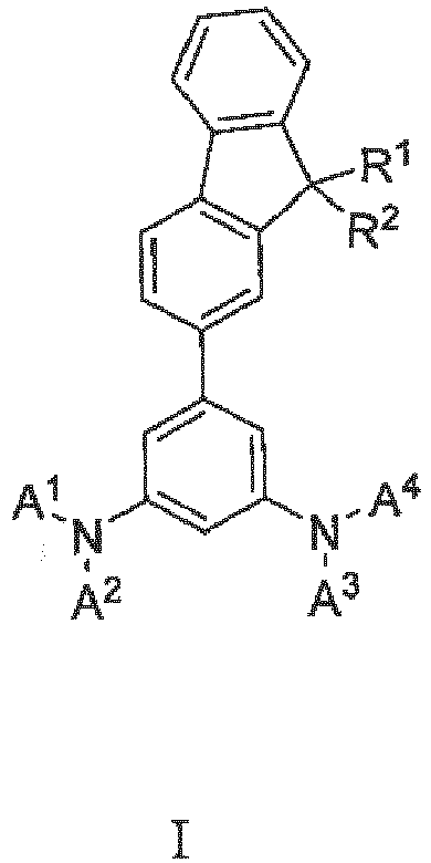
- an OLED comprising between anode and cathode at least one emitting layer comprising a phosphorescent emitter and at least one hole transporting layer comprising a compound represented by general formula (I)
- the alkyl substituents can be saturated or unsaturated, straight or branched.
- the cycloalkyl or cycloalkoxy substituent may be saturated or unsaturated, monocyclic or polycyclic.
- the overall C atom count in a substituent includes possible alkyl substitution, branching and/or occurrence of cyclic structures within the substituent.
- the overall C atom count in the compound (I) does not exceed 150. More preferably, the overall C atom count in any substituent selected from R 1 , R 2 , A 1 , A 2 , A 3 and A 4 does not exceed 20. Most preferably, the overall C atom count in any substituents selected from R 1 , R 2 , A 1 , A 2 , A 3 and A 4 does not exceed 12.
- At least one aryl selected from A 1 and A 2 and at least one aryl selected from A 3 and A 4 are C 6 -C 15 aryls.
- substituents A 1 , A 2 , A 3 and A 4 are C 6 -C 15 aryls.
- aryl substituents A 1 , A 2 , A 3 and A 4 are selected from phenyl, tolyl, xylyl, trimethylphenyl, tert-butylphenyl, 1,1'-biphenyl-yl, naphtyl and 9H-fluorenyl.
- aryl substituents A 1 , A 2 , A 3 and A 4 are selected from 1,1'-biphenyl-yl and 9H-fluorenyl.
- 1,1'-biphenyl-yl is 1,1'-biphenyl-4-yl and fluorenyl is 9,9'-dimethyl-9H-fluoren-2-yl.
- R 1 and R 2 are independently selected from C 1 -C 12 alkyl. Preferred are also all possible combinations of preferred embodiments mentioned above.
- the layer comprising compound (I) is located between the emitting layer and the anode. It is further preferred that at least one layer containing the compound of formula (I) is electrically doped.
- the electrically doped layer containing compound of formula (I) is adjacent to another, electrically undoped layer comprising compound of formula (I). Even more preferably, the undoped layer comprising compound (I) serves as electron blocking layer.
- electrical doping means generally an improvement of electrical properties, especially the electrical conductivity, in the electrically doped semiconducting material if compared with an undoped matrix material. More detailed explanation of current theory and various examples of electrical doping are available in many published patent documents, e.g. WO2014/037512 .
- the undoped layer serves as both electron-blocking and triplet exciton blocking layer.
- the alkyl substituents can be saturated or unsaturated, straight or branched.
- the cycloalkyl or cycloalkoxy substituent may be saturated or unsaturated, monocyclic or polycyclic.
- the overall C atom count in a substituent includes possible alkyl substitution, branching and/or occurrence of cyclic structures within the substituent.
- the overall C atom count in the compound (I) does not exceed 150. More preferably, the overall C atom count in any substituent selected from R 1 , R 2 , A 1 , A 2 , A 3 and A 4 does not exceed 20. Most preferably, the overall C atom count in any substituents selected from R 1 , R 2 , A 1 , A 2 , A 3 and A 4 does not exceed 12.
- At least one aryl selected from A 1 and A 2 and at least one aryl selected from A 3 and A 4 are C 6 -C 15 aryls.
- substituents A 1 , A 2 , A 3 and A 4 are C 6 -C 15 aryls.
- aryl substituents A 1 , A 2 , A 3 and A 4 are selected from phenyl, tolyl, xylyl, trimethylphenyl, tert-butylphenyl, 1,1'-biphenyl-yl, naphtyl and 9H-fluorenyl.
- aryl substituents A 1 , A 2 , A 3 and A 4 are selected from 1,1'-biphenyl-yl and 9H-fluorenyl.
- 1,1'-biphenyl-yl is 1,1'-biphenyl-4-yl and fluorenyl is 9,9'-dimethyl-9H-fluoren-2-yl.
- R 1 and R 2 are independently selected from C 1 -C 12 alkyl. Preferred are also all possible combinations of preferred embodiments mentioned above.
- alkylaryl derivatives for example were described (see e.g. EP 687 668 or JP H03-094260 ).
- Other examples comprising a fluorenyl core can be found in US 2008/0124573 . While performing detailed investigations into performance-limiting factors, it was surprisingly found by the inventors that some derivatives with similar core structures perform unexpectedly well when used in OLEDs containing a phosphorescent emitter, see PCT/EP2013/071742 .
- Emitting layer electron transporting layer, hole blocking layer, electrodes
- inventive phosphorescent light emitting device than the inventive hole transporting and/or electron blocking layer can be prepared in various designs and from various materials described in the scientific and patent literature.
- 1,3,5-Tribromobenzene the fluorenyboronic acid and Pd(PPh 3 ) 4 were dissolved in a mixture of toluene and ethanol. A degassed 2M aqueous Na 2 CO 3 solution was added. The mixture was refluxed for 18-22 hours. After cooling to room temperature, the layers were separated and the organic layer was washed with water, dried and evaporated. The crude product was purified by column chromatography (SiO 2 , hexane:DCM mixtures) giving the pure product. In TLC, the upper main spot was identified as the desired product and the one below as the 1,3-bis-fluorenyl bromobenzene side product.
- the bromoaryl component, palladium(II)acetate, cesium carbonate and 2,2'-bis(diphenylphosphino)-1,1'-binaphthyl (BINAP) were combined in a flask and dissolved in 1,4-dioxane.
- the primary arylamine component was added, followed by heating up the mixture to reflux and stirring for 16-48 hours until, according to TLC, the reaction was complete.
- the mixture was cooled to room temperature and filtered through a pad of silica gel. After washing with DCM, the organic layer was washed twice with 2M aqueous HCl, once with half-saturated Na 2 CO 3 and once with water.
- the crude product was purified by column chromatography (SiO 2 , hexane:DCM mixtures). The combined fractions were evaporated to dryness. The crude product was purified by recrystallization from hexane.
- the dibromoaryl component, the secondary amine, bis(dibenzylidenaceton)palladium, tri- tert -butylphosphine and potassium- tert -butoxide were combined in a flask and dissolved in toluene.
- the mixture was stirred at 80 °C until TLC indicated complete consumption of the starting materials (usually for 90 to 210 minutes) and then cooled to room temperature.
- the mixture was filtered through a pad of silica gel, washed with DCM and evaporated to dryness.
- the crude product was stirred in boiling methanol, hexane or acetone. After cooling to room temperature, the mixture was filtered to yield the product.
- OLED organic light emitting diodes
- the diodes were processed in vacuum via vapor thermal deposition of organic materials (active layers) and metals (electrodes). Shadow mask techniques were used to structure the devices (active matrix, electrodes).
- ITO indium tin oxide
- 16 identical indium tin oxide (ITO) substrates were processed at once in a 4x4 array placed on a table which is pivotable around its vertical axe. Using shutters, each of these 16 substrates can be covered by different set of organic layers.
- ITO indium tin oxide
- the ITO substrates were cleaned and put into a vapor thermal deposition unit in the 4x4 array.
- a reference p-doped layer e.g. H-1 doped with D1; weight ratio (97:3) was deposited on half of these substrates for a final film thickness of 30 nm.
- the studied inventive material was codeposited with the same p-dopant at the same 97:3 weight ratio and thickness.
- the second (electron blocking) layer is deposited on top of the first layer.
- half the plate is covered with 10 nm of the reference compound (e.g., TCTA) and the other half with the same inventive material as used in the first layer (see figure 1 ).
- the reference devices ( figure 1 , field D) were thus always processed together with the devices comprising the inventive materials. This approach allows assessing performance of new material in comparison with the reference independent from possible day-to-day variations of deposition rates, vacuum quality or other tool performance parameters. As each field contains 16 identically prepared OLEDs and the performance parameters were estimated for each of these 16 OLEDs, statistical evaluation of the obtained experimental results unequivocally showed the statistical significance of the observed average values reported in the Table 1.
- the subsequent phosphorescent green emission layer (Merck_TMM004:Irrpy at weight ratio 9:1) was deposited with a thickness of 20 nm, followed by 20 nm Merck_TMM004 as a hole blocking layer and 25 nm E-2 layer doped with D3 (20 weight %).
- the cathode was prepared by vacuum deposition of 100 nm aluminum layer.
- Table 1 shows the experimental results obtained by the procedure described in detail in the examples below.
- the hole transporting layer was doped with a p-dopant, what is symbolized with the p- symbol in the substrate/HTL/EBL column.
- negative values were assigned in the voltage column.
- a positive value in the voltage column shows unfavourable, higher average voltage observed at the set of devices comprising inventive compound in comparison with the average voltage measured on the set of reference devices prepared under the same conditions.
- the efficiency column the average efficiency of devices comprising an inventive compound higher than the average efficiency of comparative devices is positive, whereas unfavourable lower efficiency in comparison with reference has negative sign.
- the last column in the table shows the arithmetic difference between the value in the efficiency column and the value in the voltage column.
- the resulting value was used as a benchmark for assessing the overall performance. Its positive value in at least one from the three rows shows that at least in one application - if the compound was used as an EBL, as an HTL, or in both layers - shows that in this particular case, the percentage voltage improvement has overweighed the percentage efficiency decrease or, oppositely, that the percentage efficiency improvement overweighed the undesired voltage increase, or that there was an improvement in both properties.
- Table 1 Compound tested Core substit. Periphery s.
- inventive compounds are advantageous also when used as hole transporting and/or electron blocking matrices in blue fluorescent OLEDs.
Landscapes
- Chemical & Material Sciences (AREA)
- Physics & Mathematics (AREA)
- Organic Chemistry (AREA)
- Spectroscopy & Molecular Physics (AREA)
- Engineering & Computer Science (AREA)
- Materials Engineering (AREA)
- Optics & Photonics (AREA)
- Electroluminescent Light Sources (AREA)
Description
- The present invention relates to phosphorescent organic light-emitting devices, and to compounds which may be used in such devices, especially in hole transporting and/or electron blocking layers thereof.
- In OLEDs, the electroluminescence (EL) property of certain organic materials is used. In EL devices, suitable charge carriers are formed under application of a voltage across the device. Recombination of these charge carriers results in an excited state, which relaxes to the ground state under light emission. To increase the efficiency, the organic light-emitting diodes very often have, besides the emission layer, also charge transporting layers which are responsible for transport of negative and positive charge carriers into the emission layer. These charge transporting layers are grouped, depending on the charge carrier transported, into hole conductors and electron conductors. A quite similar set of layers is known for photovoltaic devices, such as organic solar cells. Organic semiconducting devices having several layers are produced by known methods, for example evaporation under vacuum or deposition from solution.
- In other words, in case of organic light-emitting diodes, light is produced and emitted by the injection of charge carriers, electrons from one side, holes from the other, from the contacts into adjacent organic layers as a result of an externally applied voltage, subsequent formation of excitons (electron-hole pairs) and their radiative recombinationin a recombination zone.
- The state-of-the-art OLED structure with the positive electrode (anode) adjacent to the substrate is schematically shown in
Fig. 1 , wherein the numbers 1-9 denominate the following layers: - 1. Transparent substrate
- 2. Transparent anode as bottom, hole injecting electrode
- 3. Hole-injecting layer
- 4. Hole-transporting layer (HTL)
- 5. Light-emitting layer (EML)
- 6. Electron-transporting layer (ETL)
- 7. Electron-injecting layer (EIL)
- 8. Cathode as top electrode (usually a metal with low work function, electron-injecting)
- 9. Encapsulation to protect from moisture, oxygen and other outside factors which may affect stability or efficiency.
- While this description represents the most common case, often several layers may be omitted, or else one layer may fulfill several functions.
- An important property of organic semiconducting materials is their conductivity. The conductivity of a thin layer sample can be measured by, for example, by the two-point method. A voltage is applied to the thin layer and the current flowing through the layer is measured. The measured resistance or conductivity, respectively, can be calculated from the geometry of the contacts and the thickness of the layer of the sample.
- In an OLED, the operational voltage (or, more exactly, the overall electrical resistance) is determined not only by resistances and thicknesses of particular layers, but also by energetic barriers for charge carrier injection from a particular layer to the adjacent one. The power efficiency of the device (conversion of the electrical power in the light flux at the given wavelength or in the given colour range) depends on (a) Joule losses caused by the overall resistance and on (b) the efficiency of conversion of charge carriers into photons. The latter depends predominantly on the charge carrier (electron-hole) balance and on the quantum efficiency of radiative recombination of the electron-hole pairs (excitons) in the device.
- There has been steady effort to develop materials and OLED designs which minimize Joule losses, improve charge carrier balance and maximize the quantum efficiency. Joule losses have been reduced significantly through improved charge injecting layers and the introduction of electrically doped charge transporting layers (see e.g.
WO2003/070822 orWO2005/086251 and references cited therein). Specific charge injecting and blocking layers can also improve the charge carrier balance. A further improvement in quantum efficiency has been obtained through phosphorescent emitters, which allow in theory 100 % efficiency as all excitons formed can decay radiatively. By comparison, in fluorescent emitters triplet and singled excitons are formed, but only singlet excitons can decay radiatively. Therefore, the quantum efficiency in fluorescent emitters is less than 100 %. - A number of materials used for preparing hole transport layers and/or electron/exciton blocking layers are known.
- However, the OLED efficiency is still significantly below its theoretical limits and many other OLED-performance parameters like luminosity and lifetime can be also further improved.
- From a practical point of view, it is advantageous that one matrix compound is suitable for various OLED designs, e.g. in phosphorescent as well as fluorescent OLEDs, and in both electrically doped hole injecting and/or hole transporting layers as well as in electrically undoped electron blocking layers.
- It is therefore an object of the present invention to provide improved phosphorescent OLEDs having lower operating voltage and/or higher efficiency than devices using hole transporting and electron blocking matrices according to the state of the art. Another object of the inventtion is providing new compounds which can be used as matrix materials for hole-transporting layers and/or electron/exciton blocking layers which overcome the drawbacks of the prior art and can especially be used in phosphorescent OLEDs.
- This object is achieved by an OLED comprising between anode and cathode at least one emitting layer comprising a phosphorescent emitter and at least one hole transporting layer comprising a compound represented by general formula (I)

- wherein R1 and R2 can be independently selected from hydrogen, C1-C20 alkyl or C3-C20 cycloalkyl, C7-C20 arylalkyl, C6-C12 aryl,
- A1, A2, A3 and A4 are independently selected from C6-C20 aryl, and the substituents R1 and R2 may be linked so that they form a ring.
- The alkyl substituents can be saturated or unsaturated, straight or branched. The cycloalkyl or cycloalkoxy substituent may be saturated or unsaturated, monocyclic or polycyclic. The overall C atom count in a substituent includes possible alkyl substitution, branching and/or occurrence of cyclic structures within the substituent. Preferably, the overall C atom count in the compound (I) does not exceed 150. More preferably, the overall C atom count in any substituent selected from R1, R2, A1, A2, A3 and A4 does not exceed 20. Most preferably, the overall C atom count in any substituents selected from R1, R2, A1, A2, A3 and A4 does not exceed 12.
- In a preferred embodiment, in each pair of aryl substituents attached to the same nitrogen, at least one aryl selected from A1 and A2 and at least one aryl selected from A3 and A4 are C6-C15 aryls. In a more preferred embodiment, substituents A1, A2, A3 and A4 are C6-C15 aryls. In another preferred embodiment, aryl substituents A1, A2, A3 and A4 are selected from phenyl, tolyl, xylyl, trimethylphenyl, tert-butylphenyl, 1,1'-biphenyl-yl, naphtyl and 9H-fluorenyl. In more preferred embodiment, aryl substituents A1, A2, A3 and A4 are selected from 1,1'-biphenyl-yl and 9H-fluorenyl. In an even more preferred embodiment, 1,1'-biphenyl-yl is 1,1'-biphenyl-4-yl and fluorenyl is 9,9'-dimethyl-9H-fluoren-2-yl. In another preferred embodiment, R1 and R2 are independently selected from C1-C12 alkyl. Preferred are also all possible combinations of preferred embodiments mentioned above.
- It is preferred that the layer comprising compound (I) is located between the emitting layer and the anode. It is further preferred that at least one layer containing the compound of formula (I) is electrically doped.
- More preferably, the electrically doped layer containing compound of formula (I) is adjacent to another, electrically undoped layer comprising compound of formula (I). Even more preferably, the undoped layer comprising compound (I) serves as electron blocking layer.
- The term "electrical doping" means generally an improvement of electrical properties, especially the electrical conductivity, in the electrically doped semiconducting material if compared with an undoped matrix material. More detailed explanation of current theory and various examples of electrical doping are available in many published patent documents, e.g.
WO2014/037512 . - In one yet preferred embodiment, the undoped layer serves as both electron-blocking and triplet exciton blocking layer.
- A further object is achieved by compound represented by general formula (I)

- wherein R1 and R2 can be independently selected from hydrogen, C1-C20 alkyl or C3-C20 cycloalkyl, C7-C20 arylalkyl, C6-C12 aryl,
- A1, A2, A3 and A4 are independently selected from C6-C20 aryl, and the substituents R1 and R2 may be linked so that they form a ring.
- The alkyl substituents can be saturated or unsaturated, straight or branched. The cycloalkyl or cycloalkoxy substituent may be saturated or unsaturated, monocyclic or polycyclic. The overall C atom count in a substituent includes possible alkyl substitution, branching and/or occurrence of cyclic structures within the substituent. Preferably, the overall C atom count in the compound (I) does not exceed 150. More preferably, the overall C atom count in any substituent selected from R1, R2, A1, A2, A3 and A4 does not exceed 20. Most preferably, the overall C atom count in any substituents selected from R1, R2, A1, A2, A3 and A4 does not exceed 12.
- In a preferred embodiment, in each pair of aryl substituents attached to the same nitrogen, at least one aryl selected from A1 and A2 and at least one aryl selected from A3 and A4 are C6-C15 aryls. In a more preferred embodiment, substituents A1, A2, A3 and A4 are C6-C15 aryls. In another preferred embodiment, aryl substituents A1, A2, A3 and A4 are selected from phenyl, tolyl, xylyl, trimethylphenyl, tert-butylphenyl, 1,1'-biphenyl-yl, naphtyl and 9H-fluorenyl. In more preferred embodiment, aryl substituents A1, A2, A3 and A4 are selected from 1,1'-biphenyl-yl and 9H-fluorenyl. In an even more preferred embodiment, 1,1'-biphenyl-yl is 1,1'-biphenyl-4-yl and fluorenyl is 9,9'-dimethyl-9H-fluoren-2-yl. In another preferred embodiment, R1 and R2 are independently selected from C1-C12 alkyl. Preferred are also all possible combinations of preferred embodiments mentioned above.
- Among well-known hole-transporting materials with triarylamine and benzidine structures, some alkylaryl derivatives, for example

EP 687 668 JP H03-094260 US 2008/0124573 . While performing detailed investigations into performance-limiting factors, it was surprisingly found by the inventors that some derivatives with similar core structures perform unexpectedly well when used in OLEDs containing a phosphorescent emitter, seePCT/EP2013/071742 - Further research helped clarifying relationships with the structure of the compounds tested and revealed that the presence of a fluorenyl substituent directly attached to the meta-diaminophenyl core is particularly advantageous and allows good performance of such compounds as HTL and/or EBL matrices in phosphorescent OLEDs.
- Emitting layer, electron transporting layer, hole blocking layer, electrodes
- Other parts of the inventive phosphorescent light emitting device than the inventive hole transporting and/or electron blocking layer can be prepared in various designs and from various materials described in the scientific and patent literature.
- In the examples, following supporting materials were used:

US 2010/102709 ),
WO 2013/079217 ),
WO 2013/079676 ),


WO2011/134458 andUS2012/223296 as comparative hole transporting matrices. -
-
Figure 1 : Schematic drawing of experimental bottom emitting phosphorescent OLED -
Figure 2: a ) Top view of deposition of layer 1 (p-doped inventive material (stripes), p-doped reference (dots), left;b ) Top view oflayer 2 after rotation of substrate by 90°, with the inventive material in the top row (fields A, C) and reference material in the bottom row (fields B, D). -
Figure 3a - 3j : 1H-NMR spectra of example compounds having formula (I) measured in CD2Cl2 solution, at 500.13 MHz, referenced to 5.31 ppm; 3a -FPD-1, 3b - FPD -2, 3c - FPD -3, 3d - FPD -4, 3e - FPD -5, 3f - FPD -6, 3g - FPD -7, 3h - FPD -8, 3i - FPD -9, 3j - FPD-10. - 1,3,5-Tribromobenzene, the fluorenyboronic acid and Pd(PPh3)4 were dissolved in a mixture of toluene and ethanol. A degassed 2M aqueous Na2CO3 solution was added. The mixture was refluxed for 18-22 hours. After cooling to room temperature, the layers were separated and the organic layer was washed with water, dried and evaporated. The crude product was purified by column chromatography (SiO2, hexane:DCM mixtures) giving the pure product. In TLC, the upper main spot was identified as the desired product and the one below as the 1,3-bis-fluorenyl bromobenzene side product.
-

- 1,3,5-tribromobenzene: 126.93 g (1.2 eq, 403.2 mmol)
- (9,9-dimethyl-9H-fluoren-2-yl)boronic acid: 80.00 g (1.0 eq, 336.0 mmol)
- Pd(PPh3)4: 19.4 mg (5 mol.%, 16.8 mmol)
- toluene: 960 mL
- ethanol: 320 mL
- 2M Na2CO3: 640 mL
- Yield: 69.4 g (48 %)
- GC-MS: m/z = 426 / 428 / 430
- Under an inert atmosphere, the bromoaryl component, palladium(II)acetate, cesium carbonate and 2,2'-bis(diphenylphosphino)-1,1'-binaphthyl (BINAP) were combined in a flask and dissolved in 1,4-dioxane. The primary arylamine component was added, followed by heating up the mixture to reflux and stirring for 16-48 hours until, according to TLC, the reaction was complete. The mixture was cooled to room temperature and filtered through a pad of silica gel. After washing with DCM, the organic layer was washed twice with 2M aqueous HCl, once with half-saturated Na2CO3 and once with water. After evaporation of the solvent, the crude product was purified by column chromatography (SiO2, hexane:DCM mixtures). The combined fractions were evaporated to dryness. The crude product was purified by recrystallization from hexane.
-
- 4-bromobiphenyl: 20.00 g (1.0 eq, 85.80 mmol)
- aniline: 8.39 g (1.05 eq, 90.09 mmol)
- palladium(II)acetate: 578 mg (3.0 mol.%, 2.57 mmol)
- BINAP: 2.40 g (4.5 mol.%, 3.86 mmol)
- cesium carbonate: 39.13 g (1.4 eq, 120.1 mmol)
- dioxane: 200 mL
- Yield: 11.05 g (52 %)
- GC-MS: m/z = 245
-

- 4-bromobiphenyl: 20.0 g (1.0 eq, 85.8 mmol)
- 4-toluidine: 9.65 g (1.05 eq, 90.1 mmol)
- palladium(II)acetate: 578 mg (3.0 mol.%, 2.6 mmol)
- BINAP: 2.40 g (4.5 mol.%, 3.9 mmol)
- cesium carbonate: 39.14 g (1.4 eq, 120.1 mmol)
- dioxane: 200 mL
- Yield: 19.20 g (86 %)
- GC-MS: m/z = 259
-

- 4-bromobiphenyl: 30.00 g (1.0 eq, 128.70 mmol)
- 3,5-dimethylaniline: 16.38 g (1.05 eq, 135.10 mmol)
- palladium(II)acetate: 867 mg (3.0 mol.%, 3.86 mmol)
- BINAP: 3.60 g (4.5 mod.%, 5.79 mmol)
- cesium carbonate: 58.70 g (1.4 eq, 180.00 mmol)
- dioxane: 300 mL
- Yield: 21.34 g (60 %)
- GC-MS: m/z = 273
-
- 4-bromobiphenyl: 30.00 g (1.0 eq, 128.70 mmol)
- 3,5-dimethylaniline: 16.38 g (1.05 eq, 135.10 mmol)
- palladium(II)acetate: 867 mg (3.0 mol.%, 3.86 mmol)
- BINAP: 3.60 g (4.5 mol.%, 5.79 mmol)
- cesium carbonate: 58.70 g (1.4 eq, 180.00 mmol)
- dioxane: 300 mL
- Yield: 24.40 g (69 %)
- GC-MS: m/z = 273
-

- 4-bromobiphenyl: 20.00 g (1.0 eq, 85.8 mmol)
- mesitylamine: 12.18 g (1.05 eq, 90.1 mmol)
- palladium(II)acetate: 578 mg (3.0 mol.%, 2.57 mmol)
- BINAP: 2.40 g (4.5 mol.%, 3.86 mmol)
- cesium carbonate: 39.13 g (1.4 eq, 120.1 mmol)
- dioxane: 200 mL
- Yield: 12.53 g (51 %)
- GC-MS: m/z = 287
-

- 4-bromobiphenyl: 20.00 g (1.0 eq, 85.80 mmol)
- biphenylamine: 15.25 g (1.05 eq, 90.09 mmol)
- palladium(II)acetate: 578 mg (3.0 mol.%, 2.57 mmol)
- BINAP: 2.40 g (4.5 mol.%, 3.86 mmol)
- cesium carbonate: 39.13 g (1.4 eq, 120.1 mmol)
- dioxane: 200 mL
- Yield: 6.57 g (23 %)
- GC-MS: m/z = 321
-

- 2-bromonaphthalene: 15 g (1.0 eq, 72.44 mmol)
- p-toluidine: 11.6 g (1.5 eq, 108.6 mmol)
- palladium(II)acetate: 488 mg (3.0 mol.%, 2.17 mmol)
- BINAP: 2.0 g (4.5 mol.%, 3.26 mmol)
- cesium carbonate: 47.20 g (2.0 eq, 144.9 mmol)
- dioxane: 150 mL
- Yield: 11.4 g (67 %)
- GC-MS: m/z = 233
-

- 2-bromonaphthalene: 20.00 g (1.0 eq, 96.59 mmol)
- m-toluidine: 15.52 g (1.5 eq, 144.89 mmol)
- palladium(II)acetate: 868 mg (4.0 mol.%, 3.86 mmol)
- BINAP: 3.61 g (6 mol.%, 5.79 mmol)
- cesium carbonate: 62.94 g (2 eq, 193.18 mmol)
- dioxane: 200 mL
- Yield: 12.82 g (56 %)
- GC-MS: m/z = 233
-

- 2-bromonaphthalene: 30.00 g (1.0 eq, 144.88 mmol)
- 3,5-dimethylaniline: 18.43 g (1.05 eq, 152.12 mmol)
- palladium(II)acetate: 976 mg (3.0 mol.%, 4.35 mmol)
- BINAP: 4.06 g (4.5 mol.%, 6.52 mmol)
- cesium carbonate: 66.10 g (1.4 eq, 202.86 mmol)
- dioxane: 300 mL
- Yield: 19.90 g (55 %)
- GC-MS: m/z = 247
-

-

- Under an inert atmosphere the dibromoaryl component, the secondary amine, bis(dibenzylidenaceton)palladium, tri-tert-butylphosphine and potassium-tert-butoxide were combined in a flask and dissolved in toluene. The mixture was stirred at 80 °C until TLC indicated complete consumption of the starting materials (usually for 90 to 210 minutes) and then cooled to room temperature. The mixture was filtered through a pad of silica gel, washed with DCM and evaporated to dryness. The crude product was stirred in boiling methanol, hexane or acetone. After cooling to room temperature, the mixture was filtered to yield the product. In case the TLC indicated still some impurities, column chromatography was used (SiO2, hexane:DCM mixtures). Finally, all tertiary amines were purified by gradient sublimation under high vacuum (10-6 mbar) conditions.
-

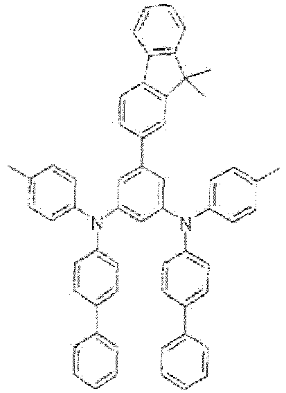
- 2-(3,5-dibromophenyl)-9,9-dimethyl-9H-fluorene: 3.0 g (1.0 eq, 7.01 mmol)
- N-phenyl-[1,1'-biphenyl]-4-amine: 3.7 g (2.1 eq, 14.71 mmol)
- bis(dibenzylidenaceton)palladium: 81 mg (2 mol.%, 0.14 mmol)
- tri-tert-butylphosphine: 43 mg (3 mol.%, 0.21 mmol)
- potassium-tert-butoxide: 2.36 g (3.0 eq, 21.03 mmol)
- toluene: 90 mL
- Yield: 4.75 g (89 %)
- EI-MS: m/z = 756 [M+]
- 1H-NMR: see
Fig. 3a -
- 2-(3,5-dibromophenyl)-9,9-dimethyl-9H-fluorene: 3.0 g (1.0 eq, 7.01 mmol)
- N-(p-tolyl)-[1,1'-bipbenyl]-4-amine: 3.82 g (2.1 eq, 14.71 mmol)
- bis(dibenzylidenaceton)palladium: 81 mg (2 mol.%, 0.14 mmol)
- tri-tert-butylphosphine: 43 mg (3 mol.%, 0.21 mmol)
- potassium-tert-butoxide: 2.36 g (3.0 eq, 21.03 mmol)
- toluene: 250 mL
- Yield: 5.32 g (96 %)
- HPLC-MS: m/z = 786 [M+H+]
- 1H-NMR: see
Fig. 3b -

- 2-(3,5-dibromophenyl)-9,9-dimethy]-9H-fluorene: 11.19 g (1.0 eq, 26.13 mmol)
- N N-(3,5-dimethylphenyl)-[1,1'-biphenyl]-4-amine: 15.00 g (2.1 eq, 54.87 mmol)
- bis(dibenzylidenaceton)palladium: 300 mg (2 mol.%, 0.52 mmol)
- tri-tert-butylphosphine: 158 mg (3 mol.%, 0.78 mmol)
- potassium-tert-butoxide: 8.80 g (3.0 eq. 78.4 mmol)
- toluene: 355 mL
- Yield: 16.66 g (78 %)
- EI-MS: m/z = 812 [M+]
- 1H-NMR: see
Fig. 3c -

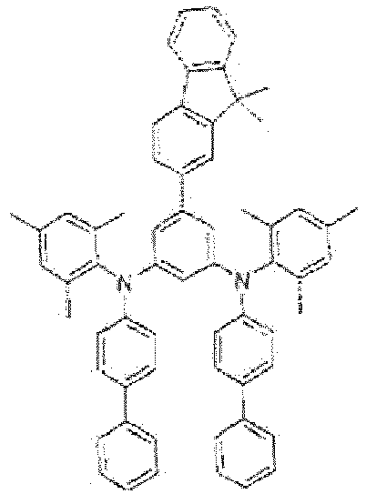
- 2-(3,5-dibromophenyl)-9,9-dimethyl-9H-fluorene: 3.0 g (1.0 eq, 7.01 mmol)
- N-(2,4-dimethylphenyl)-[1,1'-biphenyl]-4-amine: 4.0 g (2.1 eq, 14.71 mmol)
- bis(dibenzylidenaceton)palladium: 81 mg (2 mol.%, 0.14 mmol)
- tri-tert-butylphosphine: 43 mg (3 mol.%, 0.21 mmol)
- potassium-tert-butoxide: 2.36 g (3.0 eq, 21.03 mmol)
- toluene: 100 mL
- Yield: 4.46 g (78 %)
- EI-MS: m/z = 813 [M+]
- 1H-NMR: see
Fig. 3d -
- 2-(3,5-dibromophenyl)-9,9-dimethyl-9H-fluorene: 10.64 g (1.0 eq, 24.85 mmol)
- N-mesityl-[1,1'-biphenyl]-4-amine: 15.00 g (2.1 eq, 52.19 mmol)
- bis(dibenzylidenaceton)palladium: 286 mg (2 mol.%, 0.50 mmol)
- tri-tert-butylphosphine: 151 mg (3 mol.%, 0.75 mmol)
- potassium-tert-butoxide: 8.36 g (3.0 eq, 74.6 mmol)
- toluene: 335 mL
- Yield: 12.6 g (60 %)
- EI-MS: m/z = 840 [M+]
- 1H-NMR: see
Fig. 3e -
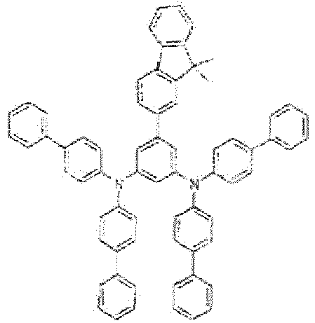
- 2-(3,5-dibromophenyl)-9,9-dimethyl-9H-fluorene: 3.0 g (1.0 eq, 7.01 mmol)
- di([1,1'-biphenyl]-4-yl)amine: 4.7 g (2.1 eq, 14.71 mmol)
- bis(dibenzylidenaceton)palladium: 81 mg (2 mol.%, 0.14 mmol)
- tri-tert-butylphosphine: 43 mg (3 mol.%, 0.21 mmol)
- potassium-tert-butoxide: 2.36 g (3.0 eq, 21.03 mmol)
- toluene: 100 mL
- Yield: 5.42 g (84 %)
- EI-MS: m/z = 908.3 [M+]
- 1H-NMR: see
Fig. 3f -
- 2-(3,5-dibromophenyl)-9,9-dimethyl-9H-fluorene: 3.0 g (1.0 eq, 7.01 mmol)
- di([1,1'-biphenyl]-4-yl)amine: 4.7 g (2.1 eq, 14.71 mmol)
- bis(dibenzylidenaceton)palladium: 81 mg (2 mol.%, 0.14 mmol)
- tri-tert-butylphosphine: 43 mg (3 mol.%, 0.21 mmol)
- potassium-tert-butoxide: 2.36 g (3.0 eq, 21.03 mmol)
- toluene: 90 mL
- Yield: 2.45 g (50 %)
- EI-MS: m/z = 704 [M+]
- 1H-NMR: see
Fig. 3g -

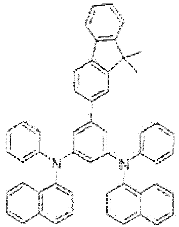
- 2-(3,5-dibromophenyl)-9,9-dimethyl-9H-fluorene: 3.0 g (1.0 eq, 7.01 mmol)
- N-phenylnaphthalen-2-amine:3.2 g (2.1 eq, 14.71 mmol)
- bis(dibenzylidenaceton)palladium: 81 mg (2 mol.%, 0.14 mmol)
- tri-tert-butylphosphine: 43 mg (3 mol.%, 0.21 mmol)
- potassium-tert-butoxide: 2.36 g (3.0 eq, 21.03 mmol)
- toluene: 90 mL
- Yield: 4.54 g (92 %)
- EI-MS: m/z = 704.6 [M+]
- 1H-NMR: see
Fig. 3h -

- 2-(3,5-dibromophenyl)-9,9-dimethyl-9H-fluorene: 3.0 g (1.0 eq, 7.01 mmol)
- N-phenylnaphthalen-2-amine: 3.4 g (2.1 eq, 14.71 mmol)
- bis(dibenzylidenaceton)palladium: 81 mg (2 mol.%, 0.14 mmol)
- tri-tert-butylphosphine: 43 mg (3 mol.%, 0.21 mmol)
- potassium-tert-butoxide: 2.36 g (3.0 eq, 21.03 mmol)
- toluene: 175 mL
- Yield: 5.80 g (63 %)
- EI-MS: m/z = 732 [M+]
- 1H-NMR: see
Fig. 3i -

- 2-(3,5-dibromophenyl)-9,9-dimethyl-9H-fluorene: 3.0 g (1.0 eq, 7.01 mmol)
- N-(3,5-dimethylphenyl)naphthalen-2-amine: 3.6 g (2.1 eq, 14.71 mmol)
- bis(dibenzylidenaceton)palladium: 81 mg (2 mol.%, 0.14 mmol)
- tri-tert-butylphosphine: 43 mg (3 mol.%, 0.21 mmol)
- potassium-tert-butoxide: 2.36 g (3.0 eq, 21.03 mmol)
- toluene: 150 mL
- Yield: 4.96 g (65 %)
- EI-MS: m/z = 760 [M+]
- 1H-NMR: see
Fig. 3j - Performance testing of the new materials was carried out in bottom emitting phosphorescent organic light emitting diodes (OLED). The diodes were processed in vacuum via vapor thermal deposition of organic materials (active layers) and metals (electrodes). Shadow mask techniques were used to structure the devices (active matrix, electrodes). Four OLEDs are prepared on one substrate with an active area of 6.70 mm2 each. 16 identical indium tin oxide (ITO) substrates were processed at once in a 4x4 array placed on a table which is pivotable around its vertical axe. Using shutters, each of these 16 substrates can be covered by different set of organic layers.
- The ITO substrates were cleaned and put into a vapor thermal deposition unit in the 4x4 array. A reference p-doped layer (e.g. H-1 doped with D1; weight ratio (97:3) was deposited on half of these substrates for a final film thickness of 30 nm. On the other half of the plate, the studied inventive material was codeposited with the same p-dopant at the same 97:3 weight ratio and thickness. After a rotation of the plate by 90°, the second (electron blocking) layer is deposited on top of the first layer. Here, half the plate is covered with 10 nm of the reference compound (e.g., TCTA) and the other half with the same inventive material as used in the first layer (see
figure 1 ). - The reference devices (
figure 1 , field D) were thus always processed together with the devices comprising the inventive materials. This approach allows assessing performance of new material in comparison with the reference independent from possible day-to-day variations of deposition rates, vacuum quality or other tool performance parameters. As each field contains 16 identically prepared OLEDs and the performance parameters were estimated for each of these 16 OLEDs, statistical evaluation of the obtained experimental results unequivocally showed the statistical significance of the observed average values reported in the Table 1. - The subsequent phosphorescent green emission layer (Merck_TMM004:Irrpy at weight ratio 9:1) was deposited with a thickness of 20 nm, followed by 20 nm Merck_TMM004 as a hole blocking layer and 25 nm E-2 layer doped with D3 (20 weight %). The cathode was prepared by vacuum deposition of 100 nm aluminum layer.
- Table 1 shows the experimental results obtained by the procedure described in detail in the examples below. In the experimental OLEDs tested, the hole transporting layer was doped with a p-dopant, what is symbolized with the p- symbol in the substrate/HTL/EBL column. In the table, to the compounds showing voltage lower voltage than reference, negative values were assigned in the voltage column. Oppositely, a positive value in the voltage column shows unfavourable, higher average voltage observed at the set of devices comprising inventive compound in comparison with the average voltage measured on the set of reference devices prepared under the same conditions. In the efficiency column, the average efficiency of devices comprising an inventive compound higher than the average efficiency of comparative devices is positive, whereas unfavourable lower efficiency in comparison with reference has negative sign. The last column in the table shows the arithmetic difference between the value in the efficiency column and the value in the voltage column. The resulting value was used as a benchmark for assessing the overall performance. Its positive value in at least one from the three rows shows that at least in one application - if the compound was used as an EBL, as an HTL, or in both layers - shows that in this particular case, the percentage voltage improvement has overweighed the percentage efficiency decrease or, oppositely, that the percentage efficiency improvement overweighed the undesired voltage increase, or that there was an improvement in both properties. The gained knowledge was exploited for providing new hole transporting and electron-blocking matrix materials, particularly useful in OLEDs comprising triplet emitters.
Table 1 Compound tested Core substit. Periphery s. phosphorescent green substrate/HTL/EBL voltage change [%] Q eff change [%] Q - voltage [%] H-1 4,4"terphenyl biphenyl-4-yl ITO / p-H-1 /H-1 -8 -38 -30 biphenyl-4-yl H-2 4,4"terphenyl 1-naphthyl phenyl ITO / p-H-1 / H-2 -8 -49 -41 ITO / p-H-2 / H-2 -8 -50 -42 TCTA triphenylamine carbazole ITO / p-H-1 / TCTA 0 reference ITO / p- TCTA / TCTA +38 +5 FPD-1 9H-fluorenyl biphenyl-4-yl phenyl ITO / p-H-1 / MPD-1 -11 -5 6 ITO / p-MPD-1 / TCTA +3 +5 2 ITO / p-MPD-1/ MPD-1 -9 -2 7 FPD-2 9H-fluorenyl biphenyl-4-yl p-tolyl ITO / p-H-1 / MPD-2 -12 -16 -4 ITO / p-MPD-2/ TCTA +5 +10 5 ITO / p-MPD-2/ MPD-2 -11 -8 3 FPD-3 9H-fluorenyl biphenyl-4-yl 3,5-dimethylphenyl ITO / p-H-1 / MPD-3 -12 -9 3 ITO / p-MPD-3 / TCTA +7 +10 3 ITO / p-MPD-3/ MPD-3 -10 -3 7 FPD-4 9H-fluorenyl biphenyl-4-yl 2,4-dimethylphenyl ITO / p-H-1 / MPD-4 -11 -1 10 ITO / p-MPD-4 / TCTA +6 +5 -1 ITO / p-MPD-4/ MPD-4 -11 1 12 FPD-5 9H-fluorenyl biphenyl-4-yl mesityl ITO / p-H-1 / MPD-5 -11 -2 9 ITO / p-MPD-5 / TCTA +8 +12 4 ITO / p-MPD-5/ MPD-5 -5 +9 14 FPD-6 9H-fluorenyl biphenyl-4-yl biphenyl-4-yl ITO / p-H-1/MPD-6 -11 -13 -2 ITO / p-MPD-6 / TCTA 0 +1 1 ITO / p-MPD-6/ MPD-6 -11 -12 -1 FPD-7 9H-fluorenyl phenyl 1-naphtyl ITO / p-H-1 / MPD-7 -9 -57 -48 ITO / p-MPD-7 / TCTA +3 +5 2 ITO / p-MPD-71 MPD-7 -4 -54 -50 - Additionally, it has been found that inventive compounds are advantageous also when used as hole transporting and/or electron blocking matrices in blue fluorescent OLEDs.
- The features disclosed in the foregoing description and in the claims may, both separately and in any combination, be material for realizing the invention in diverse forms thereof.
-
- OLED
- organic light emitting device
- EL
- electroluminescence, electroluminescent
- ETL
- electron transport layer
- HTL
- hole transport layer
- EBL
- electron blocking layer
- HBL
- hole blocking layer
- EML
- emitting layer
- EIL
- electron injecting layer
- HIL
- hole injecting layer
- 1H-NMR
- proton magnetic resonance
- EI-MS
- electron impact mass spectroscopy
- BINAP
- 2,2'-bis(diphenylphosphino)-1,1'-binaphthyl
- DCM
- dichloromethane
- TLC
- thin layer chromatography
Claims (10)
- Organic light emitting device comprising between anode and cathode at least one emitting layer comprising a phosphorescent emitter and at least one hole transporting and/or electron blocking layer comprising a compound represented by general formula (I)
 wherein R1 and R2 can be independently selected from hydrogen, C1-C20 alkyl or C3-C20 cycloalkyl, C7-C20 arylalkyl, C6-C12 aryl,A1, A2, A3 and A4 are independently selected from C6-C20 aryl, and the substituents R1 and R2 may be linked so that they form a ring.
 - Device according to claim 1, wherein in each pair of aryl substituents attached to the same nitrogen, at least one aryl selected from A1 and A2 and at least one aryl selected from A3 and A4 are C6-C15 aryls.
- Device according to any of claims 1-2, wherein aryl substituents A1. A2, A3 and A4 are C6-C15 aryls.
- Device according to any of claims 1-3, wherein aryl substituents A1, A2, A3 and A4 are selected from phenyl, tolyl, xylyl, trimethylphenyl, tert-butylphenyl, 1,1'-biphenyl-yl, naphtyl and 9H-fluorenyl.
- Device according to any of claims 1-4, wherein aryl substituents A1, A2, A3 and A4 are selected from 1,1 '-biphenyl-yl and 9H-fluorenyl.
- Device according to any of claims 1-5, wherein 1,1'-biphenyl-yl is 1,1'-biphenyl-4-yl and fluorenyl is 9,9'-dimethyl-9H-fluoren-2-yl.
- Device according to any of claims 1-6, wherein R1 and R2 are independently selected from C1-C12 alkyl.
- Device according to any of claims 1-6, wherein at least one layer containing the compound of formula (I) is electrically doped.
- Device according to claim 8, wherein the electrically doped layer containing compound of formula (I) is adjacent to another, electrically undoped layer comprising compound of formula (1).
- Compound represented by general formula (I)
 wherein R1 and R2 can be independently selected from hydrogen, C1-C20 alkyl or C3-C20 cycloalkyl, C7-C20 arylalkyl, C6-C12 aryl,A1, A2, A3 and A4 are independently selected from C6-C20 aryl, and the substituents R1 and R2 may be linked so that they form a ring.
Priority Applications (4)
| Application Number | Priority Date | Filing Date | Title |
|---|---|---|---|
| EP14165200.8A EP2933852B2 (en) | 2014-04-17 | 2014-04-17 | Phosphorescent OLED and hole transporting materials for phosphorescent OLEDs |
| PCT/EP2015/058372 WO2015158886A1 (en) | 2014-04-17 | 2015-04-17 | Phosphorescent oled and hole transporting materials for phosphorescent oleds |
| TW104112316A TWI721944B (en) | 2014-04-17 | 2015-04-17 | Phosphorescent oled and hole transporting materials for phosphorescent oleds |
| US15/304,530 US20170047519A1 (en) | 2014-04-17 | 2015-04-17 | Phosphorescent OLED and Hole Transporting Materials for Phosphorescent OLEDs |
Applications Claiming Priority (1)
| Application Number | Priority Date | Filing Date | Title |
|---|---|---|---|
| EP14165200.8A EP2933852B2 (en) | 2014-04-17 | 2014-04-17 | Phosphorescent OLED and hole transporting materials for phosphorescent OLEDs |
Publications (3)
| Publication Number | Publication Date |
|---|---|
| EP2933852A1 EP2933852A1 (en) | 2015-10-21 |
| EP2933852B1 EP2933852B1 (en) | 2017-05-17 |
| EP2933852B2 true EP2933852B2 (en) | 2023-09-06 |
Family
ID=50513084
Family Applications (1)
| Application Number | Title | Priority Date | Filing Date |
|---|---|---|---|
| EP14165200.8A Active EP2933852B2 (en) | 2014-04-17 | 2014-04-17 | Phosphorescent OLED and hole transporting materials for phosphorescent OLEDs |
Country Status (4)
| Country | Link |
|---|---|
| US (1) | US20170047519A1 (en) |
| EP (1) | EP2933852B2 (en) |
| TW (1) | TWI721944B (en) |
| WO (1) | WO2015158886A1 (en) |
Families Citing this family (4)
| Publication number | Priority date | Publication date | Assignee | Title |
|---|---|---|---|---|
| KR102072917B1 (en) * | 2017-09-26 | 2020-03-02 | 주식회사 엘지화학 | Coating composition, organic light emitting device using the same and method of manufacturing the same |
| DE102018125307A1 (en) | 2018-10-12 | 2020-04-16 | Novaled Gmbh | Organic light emitting device |
| EP3742513A1 (en) | 2019-05-21 | 2020-11-25 | Novaled GmbH | Organic light emitting diode |
| CN112239475B (en) * | 2020-01-22 | 2023-03-24 | 陕西莱特光电材料股份有限公司 | Nitrogen-containing compound, electronic component, and electronic device |
Citations (10)
| Publication number | Priority date | Publication date | Assignee | Title |
|---|---|---|---|---|
| WO2001093642A1 (en) † | 2000-05-30 | 2001-12-06 | The Trustees Of Princeton University | Phosphorescent organic light emitting devices |
| JP3824385B2 (en) † | 1996-08-02 | 2006-09-20 | 三井化学株式会社 | Organic electroluminescence device |
| CN101088992A (en) † | 2007-04-04 | 2007-12-19 | 南昌大学 | Cyclic aromatic amine hole transport material with high glass transition temperature and synthesis method |
| US20080124573A1 (en) † | 2006-11-28 | 2008-05-29 | Canon Kabushiki Kaisha | Amine compound and organic light-emitting device |
| KR20110100877A (en) † | 2010-03-05 | 2011-09-15 | 덕산하이메탈(주) | Compound containing two or more compounds containing two or more five-membered heterocycle, and organic electric device using the same, the terminal |
| KR20110111095A (en) † | 2010-04-02 | 2011-10-10 | 에스에프씨 주식회사 | Heteroarylamine Derivatives and Organic Electroluminescent Devices Comprising the Same |
| US20120217492A1 (en) † | 2009-11-05 | 2012-08-30 | Duksan High Metal Co., Ltd. | Organic compound, organic electronic device using same, and terminal for same |
| US20140361269A1 (en) † | 2013-06-10 | 2014-12-11 | Samsung Display Co., Ltd. | Organic light emitting diode device |
| US20150187850A1 (en) † | 2013-12-30 | 2015-07-02 | Lg Display Co., Ltd. | Organic light emitting diode and organic light emitting diode display device including the same |
| WO2016078738A1 (en) † | 2014-11-18 | 2016-05-26 | Merck Patent Gmbh | Materials for organic electroluminescent devices |
Family Cites Families (11)
| Publication number | Priority date | Publication date | Assignee | Title |
|---|---|---|---|---|
| JPH0394260A (en) | 1989-09-06 | 1991-04-19 | Konica Corp | Electrophotographic sensitive body |
| JPH07324058A (en) | 1994-05-30 | 1995-12-12 | Mita Ind Co Ltd | M-phenylenediamine derivative and electrophotographic sensitizer using the same |
| DE10207859A1 (en) | 2002-02-20 | 2003-09-04 | Univ Dresden Tech | Doped organic semiconductor material and process for its production |
| DE102004010954A1 (en) | 2004-03-03 | 2005-10-06 | Novaled Gmbh | Use of a metal complex as an n-dopant for an organic semiconductive matrix material, organic semiconductor material and electronic component |
| JP4235619B2 (en) * | 2005-02-14 | 2009-03-11 | キヤノン株式会社 | Manufacturing method of organic light emitting device |
| JP4644751B1 (en) * | 2010-01-15 | 2011-03-02 | 富士フイルム株式会社 | Organic electroluminescence device |
| KR101766709B1 (en) | 2010-04-27 | 2017-08-09 | 노발레드 게엠베하 | Organic semiconducting material and electronic component |
| TWI526418B (en) | 2011-03-01 | 2016-03-21 | 諾瓦發光二極體股份公司 | Organic semiconductor materials and organic compositions |
| TWI584513B (en) | 2011-11-30 | 2017-05-21 | 諾瓦發光二極體有限公司 | Display |
| CN103468243B (en) * | 2012-06-06 | 2015-08-19 | 广东阿格蕾雅光电材料有限公司 | Organic electronic material and organic electroluminescence device |
| EP2706584A1 (en) | 2012-09-07 | 2014-03-12 | Novaled AG | Charge transporting semi-conducting material and semi-conducting device |
-
2014
- 2014-04-17 EP EP14165200.8A patent/EP2933852B2/en active Active
-
2015
- 2015-04-17 US US15/304,530 patent/US20170047519A1/en not_active Abandoned
- 2015-04-17 WO PCT/EP2015/058372 patent/WO2015158886A1/en not_active Ceased
- 2015-04-17 TW TW104112316A patent/TWI721944B/en active
Patent Citations (10)
| Publication number | Priority date | Publication date | Assignee | Title |
|---|---|---|---|---|
| JP3824385B2 (en) † | 1996-08-02 | 2006-09-20 | 三井化学株式会社 | Organic electroluminescence device |
| WO2001093642A1 (en) † | 2000-05-30 | 2001-12-06 | The Trustees Of Princeton University | Phosphorescent organic light emitting devices |
| US20080124573A1 (en) † | 2006-11-28 | 2008-05-29 | Canon Kabushiki Kaisha | Amine compound and organic light-emitting device |
| CN101088992A (en) † | 2007-04-04 | 2007-12-19 | 南昌大学 | Cyclic aromatic amine hole transport material with high glass transition temperature and synthesis method |
| US20120217492A1 (en) † | 2009-11-05 | 2012-08-30 | Duksan High Metal Co., Ltd. | Organic compound, organic electronic device using same, and terminal for same |
| KR20110100877A (en) † | 2010-03-05 | 2011-09-15 | 덕산하이메탈(주) | Compound containing two or more compounds containing two or more five-membered heterocycle, and organic electric device using the same, the terminal |
| KR20110111095A (en) † | 2010-04-02 | 2011-10-10 | 에스에프씨 주식회사 | Heteroarylamine Derivatives and Organic Electroluminescent Devices Comprising the Same |
| US20140361269A1 (en) † | 2013-06-10 | 2014-12-11 | Samsung Display Co., Ltd. | Organic light emitting diode device |
| US20150187850A1 (en) † | 2013-12-30 | 2015-07-02 | Lg Display Co., Ltd. | Organic light emitting diode and organic light emitting diode display device including the same |
| WO2016078738A1 (en) † | 2014-11-18 | 2016-05-26 | Merck Patent Gmbh | Materials for organic electroluminescent devices |
Non-Patent Citations (8)
| Title |
|---|
| 1UPAC, "Compendium of Chemical Terminology" International Union of Pure and Applied Chemistry (24.02.2014) † |
| G. P. Moss ET AL: "Glossary of class names of organic compounds and reactive intermediates based on structure", Pure & Appl. Chem., vol. 67, no. 8/9, 1 January 1995, pages1307 and 1320 † |
| machine translation of D4 † |
| March, Jerry, "Advanced Organic Chemistry: Reactions, Mechanism, and Structure", John Wiley & Sons, 1992, Ed. 4, p. 40-48 † |
| Rompp Chcmic Lcxikon (1995), definition of "Aryl" † |
| Streitwieser, Andrew et al., "Introduction to Organic Chemistry", Macmillian Publishing Company, 1992, Ed. 4, p. 604-610 † |
| Tokito, Shizuo et al., "Phosphorescent Organic Light-emitting Devices: Triplet Energy Management", Review - Electrochemistry, Vol. 1, No. 76, p. 24-31, 2008 † |
| YERSIN H.: "Highly Efficient OLEDs with Phosphorescent Materials", 2008, WILEY-VCH, Weinheim, pages: 1 - 4 † |
Also Published As
| Publication number | Publication date |
|---|---|
| EP2933852A1 (en) | 2015-10-21 |
| EP2933852B1 (en) | 2017-05-17 |
| TW201540695A (en) | 2015-11-01 |
| TWI721944B (en) | 2021-03-21 |
| US20170047519A1 (en) | 2017-02-16 |
| WO2015158886A1 (en) | 2015-10-22 |
Similar Documents
| Publication | Publication Date | Title |
|---|---|---|
| US10868254B2 (en) | Phosphorescent OLED and hole transporting materials for phosphorescent OLEDS | |
| TWI635069B (en) | Material for organic electroluminescent device | |
| EP2478576B9 (en) | Organic electronic device and dopant for doping an organic semiconducting matrix material | |
| US11201290B2 (en) | Tetraphenylene anthracene compounds | |
| US20070262703A1 (en) | 2,2'-Disubstituted 9,9'-Spirobifluorene-based Triaryldiamines and Their Application | |
| US10978645B2 (en) | Indolocarbazole tetraphenylene compounds | |
| US9748493B2 (en) | Aromatic amine-terphenyl compounds and use thereof in organic semiconducting components | |
| US11512038B2 (en) | Tetraphenylene triarylamine compounds | |
| CN101243157A (en) | Green electroluminescent compound and organic electroluminescent device using the same | |
| KR20160118123A (en) | Material for organic electroluminescent device and organic electroluminescent device using the same | |
| EP2933852B2 (en) | Phosphorescent OLED and hole transporting materials for phosphorescent OLEDs | |
| EP4122936B1 (en) | Novel boron compound and organic light-emitting element comprising same | |
| Huang et al. | Organic electroluminescent derivatives containing dibenzothiophene and diarylamine segments | |
| EP4077337B1 (en) | Organic molecules for optoelectronic devices | |
| CN115605490A (en) | Organic Molecules for Optoelectronic Devices | |
| KR101884624B1 (en) | Compound for organic electronic element, organic electronic element using the same, and a electronic device thereof | |
| CN112430189B (en) | Pyrene organic electroluminescent material containing aromatic amine substitution | |
| EP2924753B1 (en) | Polychromatic light emitting devices and versatile hole transporting matrix for them | |
| EP3360945B1 (en) | Organic electroluminescent device |
Legal Events
| Date | Code | Title | Description |
|---|---|---|---|
| PUAI | Public reference made under article 153(3) epc to a published international application that has entered the european phase |
Free format text: ORIGINAL CODE: 0009012 |
|
| AK | Designated contracting states |
Kind code of ref document: A1 Designated state(s): AL AT BE BG CH CY CZ DE DK EE ES FI FR GB GR HR HU IE IS IT LI LT LU LV MC MK MT NL NO PL PT RO RS SE SI SK SM TR |
|
| AX | Request for extension of the european patent |
Extension state: BA ME |
|
| 17P | Request for examination filed |
Effective date: 20160413 |
|
| RBV | Designated contracting states (corrected) |
Designated state(s): AL AT BE BG CH CY CZ DE DK EE ES FI FR GB GR HR HU IE IS IT LI LT LU LV MC MK MT NL NO PL PT RO RS SE SI SK SM TR |
|
| GRAP | Despatch of communication of intention to grant a patent |
Free format text: ORIGINAL CODE: EPIDOSNIGR1 |
|
| STAA | Information on the status of an ep patent application or granted ep patent |
Free format text: STATUS: GRANT OF PATENT IS INTENDED |
|
| RIC1 | Information provided on ipc code assigned before grant |
Ipc: H01L 51/50 20060101AFI20161018BHEP Ipc: H01L 51/54 20060101ALI20161018BHEP |
|
| INTG | Intention to grant announced |
Effective date: 20161102 |
|
| GRAS | Grant fee paid |
Free format text: ORIGINAL CODE: EPIDOSNIGR3 |
|
| RIN1 | Information on inventor provided before grant (corrected) |
Inventor name: WALLIKEWITZ, BODO Inventor name: KOEHLER, MARTIN Inventor name: ZOELLNER, MIKE |
|
| GRAA | (expected) grant |
Free format text: ORIGINAL CODE: 0009210 |
|
| STAA | Information on the status of an ep patent application or granted ep patent |
Free format text: STATUS: THE PATENT HAS BEEN GRANTED |
|
| AK | Designated contracting states |
Kind code of ref document: B1 Designated state(s): AL AT BE BG CH CY CZ DE DK EE ES FI FR GB GR HR HU IE IS IT LI LT LU LV MC MK MT NL NO PL PT RO RS SE SI SK SM TR |
|
| REG | Reference to a national code |
Ref country code: GB Ref legal event code: FG4D |
|
| REG | Reference to a national code |
Ref country code: CH Ref legal event code: EP |
|
| REG | Reference to a national code |
Ref country code: IE Ref legal event code: FG4D |
|
| REG | Reference to a national code |
Ref country code: AT Ref legal event code: REF Ref document number: 895187 Country of ref document: AT Kind code of ref document: T Effective date: 20170615 |
|
| REG | Reference to a national code |
Ref country code: DE Ref legal event code: R096 Ref document number: 602014009836 Country of ref document: DE |
|
| REG | Reference to a national code |
Ref country code: NL Ref legal event code: MP Effective date: 20170517 |
|
| REG | Reference to a national code |
Ref country code: LT Ref legal event code: MG4D |
|
| REG | Reference to a national code |
Ref country code: AT Ref legal event code: MK05 Ref document number: 895187 Country of ref document: AT Kind code of ref document: T Effective date: 20170517 |
|
| PG25 | Lapsed in a contracting state [announced via postgrant information from national office to epo] |
Ref country code: ES Free format text: LAPSE BECAUSE OF FAILURE TO SUBMIT A TRANSLATION OF THE DESCRIPTION OR TO PAY THE FEE WITHIN THE PRESCRIBED TIME-LIMIT Effective date: 20170517 Ref country code: HR Free format text: LAPSE BECAUSE OF FAILURE TO SUBMIT A TRANSLATION OF THE DESCRIPTION OR TO PAY THE FEE WITHIN THE PRESCRIBED TIME-LIMIT Effective date: 20170517 Ref country code: GR Free format text: LAPSE BECAUSE OF FAILURE TO SUBMIT A TRANSLATION OF THE DESCRIPTION OR TO PAY THE FEE WITHIN THE PRESCRIBED TIME-LIMIT Effective date: 20170818 Ref country code: FI Free format text: LAPSE BECAUSE OF FAILURE TO SUBMIT A TRANSLATION OF THE DESCRIPTION OR TO PAY THE FEE WITHIN THE PRESCRIBED TIME-LIMIT Effective date: 20170517 Ref country code: AT Free format text: LAPSE BECAUSE OF FAILURE TO SUBMIT A TRANSLATION OF THE DESCRIPTION OR TO PAY THE FEE WITHIN THE PRESCRIBED TIME-LIMIT Effective date: 20170517 Ref country code: NO Free format text: LAPSE BECAUSE OF FAILURE TO SUBMIT A TRANSLATION OF THE DESCRIPTION OR TO PAY THE FEE WITHIN THE PRESCRIBED TIME-LIMIT Effective date: 20170817 Ref country code: LT Free format text: LAPSE BECAUSE OF FAILURE TO SUBMIT A TRANSLATION OF THE DESCRIPTION OR TO PAY THE FEE WITHIN THE PRESCRIBED TIME-LIMIT Effective date: 20170517 |
|
| PG25 | Lapsed in a contracting state [announced via postgrant information from national office to epo] |
Ref country code: NL Free format text: LAPSE BECAUSE OF FAILURE TO SUBMIT A TRANSLATION OF THE DESCRIPTION OR TO PAY THE FEE WITHIN THE PRESCRIBED TIME-LIMIT Effective date: 20170517 Ref country code: SE Free format text: LAPSE BECAUSE OF FAILURE TO SUBMIT A TRANSLATION OF THE DESCRIPTION OR TO PAY THE FEE WITHIN THE PRESCRIBED TIME-LIMIT Effective date: 20170517 Ref country code: PL Free format text: LAPSE BECAUSE OF FAILURE TO SUBMIT A TRANSLATION OF THE DESCRIPTION OR TO PAY THE FEE WITHIN THE PRESCRIBED TIME-LIMIT Effective date: 20170517 Ref country code: RS Free format text: LAPSE BECAUSE OF FAILURE TO SUBMIT A TRANSLATION OF THE DESCRIPTION OR TO PAY THE FEE WITHIN THE PRESCRIBED TIME-LIMIT Effective date: 20170517 Ref country code: LV Free format text: LAPSE BECAUSE OF FAILURE TO SUBMIT A TRANSLATION OF THE DESCRIPTION OR TO PAY THE FEE WITHIN THE PRESCRIBED TIME-LIMIT Effective date: 20170517 Ref country code: BG Free format text: LAPSE BECAUSE OF FAILURE TO SUBMIT A TRANSLATION OF THE DESCRIPTION OR TO PAY THE FEE WITHIN THE PRESCRIBED TIME-LIMIT Effective date: 20170817 Ref country code: IS Free format text: LAPSE BECAUSE OF FAILURE TO SUBMIT A TRANSLATION OF THE DESCRIPTION OR TO PAY THE FEE WITHIN THE PRESCRIBED TIME-LIMIT Effective date: 20170917 |
|
| PG25 | Lapsed in a contracting state [announced via postgrant information from national office to epo] |
Ref country code: SK Free format text: LAPSE BECAUSE OF FAILURE TO SUBMIT A TRANSLATION OF THE DESCRIPTION OR TO PAY THE FEE WITHIN THE PRESCRIBED TIME-LIMIT Effective date: 20170517 Ref country code: DK Free format text: LAPSE BECAUSE OF FAILURE TO SUBMIT A TRANSLATION OF THE DESCRIPTION OR TO PAY THE FEE WITHIN THE PRESCRIBED TIME-LIMIT Effective date: 20170517 Ref country code: EE Free format text: LAPSE BECAUSE OF FAILURE TO SUBMIT A TRANSLATION OF THE DESCRIPTION OR TO PAY THE FEE WITHIN THE PRESCRIBED TIME-LIMIT Effective date: 20170517 Ref country code: CZ Free format text: LAPSE BECAUSE OF FAILURE TO SUBMIT A TRANSLATION OF THE DESCRIPTION OR TO PAY THE FEE WITHIN THE PRESCRIBED TIME-LIMIT Effective date: 20170517 Ref country code: RO Free format text: LAPSE BECAUSE OF FAILURE TO SUBMIT A TRANSLATION OF THE DESCRIPTION OR TO PAY THE FEE WITHIN THE PRESCRIBED TIME-LIMIT Effective date: 20170517 |
|
| REG | Reference to a national code |
Ref country code: DE Ref legal event code: R026 Ref document number: 602014009836 Country of ref document: DE |
|
| PLBI | Opposition filed |
Free format text: ORIGINAL CODE: 0009260 |
|
| PG25 | Lapsed in a contracting state [announced via postgrant information from national office to epo] |
Ref country code: SM Free format text: LAPSE BECAUSE OF FAILURE TO SUBMIT A TRANSLATION OF THE DESCRIPTION OR TO PAY THE FEE WITHIN THE PRESCRIBED TIME-LIMIT Effective date: 20170517 Ref country code: IT Free format text: LAPSE BECAUSE OF FAILURE TO SUBMIT A TRANSLATION OF THE DESCRIPTION OR TO PAY THE FEE WITHIN THE PRESCRIBED TIME-LIMIT Effective date: 20170517 |
|
| PLAX | Notice of opposition and request to file observation + time limit sent |
Free format text: ORIGINAL CODE: EPIDOSNOBS2 |
|
| 26 | Opposition filed |
Opponent name: MERCK PATENT GMBH Effective date: 20180215 |
|
| PG25 | Lapsed in a contracting state [announced via postgrant information from national office to epo] |
Ref country code: SI Free format text: LAPSE BECAUSE OF FAILURE TO SUBMIT A TRANSLATION OF THE DESCRIPTION OR TO PAY THE FEE WITHIN THE PRESCRIBED TIME-LIMIT Effective date: 20170517 |
|
| PLBB | Reply of patent proprietor to notice(s) of opposition received |
Free format text: ORIGINAL CODE: EPIDOSNOBS3 |
|
| PG25 | Lapsed in a contracting state [announced via postgrant information from national office to epo] |
Ref country code: MC Free format text: LAPSE BECAUSE OF FAILURE TO SUBMIT A TRANSLATION OF THE DESCRIPTION OR TO PAY THE FEE WITHIN THE PRESCRIBED TIME-LIMIT Effective date: 20170517 |
|
| REG | Reference to a national code |
Ref country code: CH Ref legal event code: PL |
|
| REG | Reference to a national code |
Ref country code: BE Ref legal event code: MM Effective date: 20180430 |
|
| GBPC | Gb: european patent ceased through non-payment of renewal fee |
Effective date: 20180417 |
|
| REG | Reference to a national code |
Ref country code: IE Ref legal event code: MM4A |
|
| PG25 | Lapsed in a contracting state [announced via postgrant information from national office to epo] |
Ref country code: LU Free format text: LAPSE BECAUSE OF NON-PAYMENT OF DUE FEES Effective date: 20180417 |
|
| PG25 | Lapsed in a contracting state [announced via postgrant information from national office to epo] |
Ref country code: BE Free format text: LAPSE BECAUSE OF NON-PAYMENT OF DUE FEES Effective date: 20180430 Ref country code: CH Free format text: LAPSE BECAUSE OF NON-PAYMENT OF DUE FEES Effective date: 20180430 Ref country code: LI Free format text: LAPSE BECAUSE OF NON-PAYMENT OF DUE FEES Effective date: 20180430 Ref country code: GB Free format text: LAPSE BECAUSE OF NON-PAYMENT OF DUE FEES Effective date: 20180417 |
|
| PG25 | Lapsed in a contracting state [announced via postgrant information from national office to epo] |
Ref country code: FR Free format text: LAPSE BECAUSE OF NON-PAYMENT OF DUE FEES Effective date: 20180430 Ref country code: IE Free format text: LAPSE BECAUSE OF NON-PAYMENT OF DUE FEES Effective date: 20180417 |
|
| RAP2 | Party data changed (patent owner data changed or rights of a patent transferred) |
Owner name: NOVALED GMBH |
|
| RIC2 | Information provided on ipc code assigned after grant |
Ipc: H01L 51/54 20060101AFI20190611BHEP |
|
| APBM | Appeal reference recorded |
Free format text: ORIGINAL CODE: EPIDOSNREFNO |
|
| APBP | Date of receipt of notice of appeal recorded |
Free format text: ORIGINAL CODE: EPIDOSNNOA2O |
|
| APAH | Appeal reference modified |
Free format text: ORIGINAL CODE: EPIDOSCREFNO |
|
| APBM | Appeal reference recorded |
Free format text: ORIGINAL CODE: EPIDOSNREFNO |
|
| APBP | Date of receipt of notice of appeal recorded |
Free format text: ORIGINAL CODE: EPIDOSNNOA2O |
|
| APAL | Date of receipt of statement of grounds of an appeal modified |
Free format text: ORIGINAL CODE: EPIDOSCNOA3O |
|
| APBQ | Date of receipt of statement of grounds of appeal recorded |
Free format text: ORIGINAL CODE: EPIDOSNNOA3O |
|
| PG25 | Lapsed in a contracting state [announced via postgrant information from national office to epo] |
Ref country code: MT Free format text: LAPSE BECAUSE OF NON-PAYMENT OF DUE FEES Effective date: 20180417 |
|
| PG25 | Lapsed in a contracting state [announced via postgrant information from national office to epo] |
Ref country code: TR Free format text: LAPSE BECAUSE OF FAILURE TO SUBMIT A TRANSLATION OF THE DESCRIPTION OR TO PAY THE FEE WITHIN THE PRESCRIBED TIME-LIMIT Effective date: 20170517 |
|
| PG25 | Lapsed in a contracting state [announced via postgrant information from national office to epo] |
Ref country code: PT Free format text: LAPSE BECAUSE OF FAILURE TO SUBMIT A TRANSLATION OF THE DESCRIPTION OR TO PAY THE FEE WITHIN THE PRESCRIBED TIME-LIMIT Effective date: 20170517 |
|
| PG25 | Lapsed in a contracting state [announced via postgrant information from national office to epo] |
Ref country code: CY Free format text: LAPSE BECAUSE OF FAILURE TO SUBMIT A TRANSLATION OF THE DESCRIPTION OR TO PAY THE FEE WITHIN THE PRESCRIBED TIME-LIMIT Effective date: 20170517 Ref country code: HU Free format text: LAPSE BECAUSE OF FAILURE TO SUBMIT A TRANSLATION OF THE DESCRIPTION OR TO PAY THE FEE WITHIN THE PRESCRIBED TIME-LIMIT; INVALID AB INITIO Effective date: 20140417 Ref country code: MK Free format text: LAPSE BECAUSE OF NON-PAYMENT OF DUE FEES Effective date: 20170517 |
|
| PG25 | Lapsed in a contracting state [announced via postgrant information from national office to epo] |
Ref country code: AL Free format text: LAPSE BECAUSE OF FAILURE TO SUBMIT A TRANSLATION OF THE DESCRIPTION OR TO PAY THE FEE WITHIN THE PRESCRIBED TIME-LIMIT Effective date: 20170517 |
|
| REG | Reference to a national code |
Ref country code: DE Ref legal event code: R079 Ref document number: 602014009836 Country of ref document: DE Free format text: PREVIOUS MAIN CLASS: H01L0051500000 Ipc: H10K0050000000 |
|
| APBU | Appeal procedure closed |
Free format text: ORIGINAL CODE: EPIDOSNNOA9O |
|
| P01 | Opt-out of the competence of the unified patent court (upc) registered |
Effective date: 20230515 |
|
| REG | Reference to a national code |
Ref country code: CH Ref legal event code: PK Free format text: BERICHTIGUNGEN |
|
| RIC2 | Information provided on ipc code assigned after grant |
Ipc: H10K 85/60 20230101ALI20230615BHEP Ipc: H10K 101/10 20230101ALI20230615BHEP Ipc: H10K 50/18 20230101ALI20230615BHEP Ipc: H10K 50/15 20230101AFI20230615BHEP |
|
| PUAH | Patent maintained in amended form |
Free format text: ORIGINAL CODE: 0009272 |
|
| STAA | Information on the status of an ep patent application or granted ep patent |
Free format text: STATUS: PATENT MAINTAINED AS AMENDED |
|
| 27A | Patent maintained in amended form |
Effective date: 20230906 |
|
| AK | Designated contracting states |
Kind code of ref document: B2 Designated state(s): AL AT BE BG CH CY CZ DE DK EE ES FI FR GB GR HR HU IE IS IT LI LT LU LV MC MK MT NL NO PL PT RO RS SE SI SK SM TR |
|
| REG | Reference to a national code |
Ref country code: DE Ref legal event code: R102 Ref document number: 602014009836 Country of ref document: DE |
|
| PGFP | Annual fee paid to national office [announced via postgrant information from national office to epo] |
Ref country code: DE Payment date: 20250225 Year of fee payment: 12 |