WO2011108603A1 - 面状照明装置およびこれを備えた液晶表示装置 - Google Patents
面状照明装置およびこれを備えた液晶表示装置 Download PDFInfo
- Publication number
- WO2011108603A1 WO2011108603A1 PCT/JP2011/054789 JP2011054789W WO2011108603A1 WO 2011108603 A1 WO2011108603 A1 WO 2011108603A1 JP 2011054789 W JP2011054789 W JP 2011054789W WO 2011108603 A1 WO2011108603 A1 WO 2011108603A1
- Authority
- WO
- WIPO (PCT)
- Prior art keywords
- sheet
- support member
- liquid crystal
- crystal display
- lighting device
- Prior art date
- Legal status (The legal status is an assumption and is not a legal conclusion. Google has not performed a legal analysis and makes no representation as to the accuracy of the status listed.)
- Ceased
Links
Images






Classifications
-
- G—PHYSICS
- G02—OPTICS
- G02B—OPTICAL ELEMENTS, SYSTEMS OR APPARATUS
- G02B5/00—Optical elements other than lenses
- G02B5/02—Diffusing elements; Afocal elements
- G02B5/0205—Diffusing elements; Afocal elements characterised by the diffusing properties
- G02B5/021—Diffusing elements; Afocal elements characterised by the diffusing properties the diffusion taking place at the element's surface, e.g. by means of surface roughening or microprismatic structures
- G02B5/0226—Diffusing elements; Afocal elements characterised by the diffusing properties the diffusion taking place at the element's surface, e.g. by means of surface roughening or microprismatic structures having particles on the surface
-
- G—PHYSICS
- G02—OPTICS
- G02F—OPTICAL DEVICES OR ARRANGEMENTS FOR THE CONTROL OF LIGHT BY MODIFICATION OF THE OPTICAL PROPERTIES OF THE MEDIA OF THE ELEMENTS INVOLVED THEREIN; NON-LINEAR OPTICS; FREQUENCY-CHANGING OF LIGHT; OPTICAL LOGIC ELEMENTS; OPTICAL ANALOGUE/DIGITAL CONVERTERS
- G02F1/00—Devices or arrangements for the control of the intensity, colour, phase, polarisation or direction of light arriving from an independent light source, e.g. switching, gating or modulating; Non-linear optics
- G02F1/01—Devices or arrangements for the control of the intensity, colour, phase, polarisation or direction of light arriving from an independent light source, e.g. switching, gating or modulating; Non-linear optics for the control of the intensity, phase, polarisation or colour
- G02F1/13—Devices or arrangements for the control of the intensity, colour, phase, polarisation or direction of light arriving from an independent light source, e.g. switching, gating or modulating; Non-linear optics for the control of the intensity, phase, polarisation or colour based on liquid crystals, e.g. single liquid crystal display cells
- G02F1/133—Constructional arrangements; Operation of liquid crystal cells; Circuit arrangements
- G02F1/1333—Constructional arrangements; Manufacturing methods
- G02F1/1335—Structural association of cells with optical devices, e.g. polarisers or reflectors
- G02F1/1336—Illuminating devices
- G02F1/133602—Direct backlight
- G02F1/133606—Direct backlight including a specially adapted diffusing, scattering or light controlling members
-
- G—PHYSICS
- G02—OPTICS
- G02F—OPTICAL DEVICES OR ARRANGEMENTS FOR THE CONTROL OF LIGHT BY MODIFICATION OF THE OPTICAL PROPERTIES OF THE MEDIA OF THE ELEMENTS INVOLVED THEREIN; NON-LINEAR OPTICS; FREQUENCY-CHANGING OF LIGHT; OPTICAL LOGIC ELEMENTS; OPTICAL ANALOGUE/DIGITAL CONVERTERS
- G02F1/00—Devices or arrangements for the control of the intensity, colour, phase, polarisation or direction of light arriving from an independent light source, e.g. switching, gating or modulating; Non-linear optics
- G02F1/01—Devices or arrangements for the control of the intensity, colour, phase, polarisation or direction of light arriving from an independent light source, e.g. switching, gating or modulating; Non-linear optics for the control of the intensity, phase, polarisation or colour
- G02F1/13—Devices or arrangements for the control of the intensity, colour, phase, polarisation or direction of light arriving from an independent light source, e.g. switching, gating or modulating; Non-linear optics for the control of the intensity, phase, polarisation or colour based on liquid crystals, e.g. single liquid crystal display cells
- G02F1/133—Constructional arrangements; Operation of liquid crystal cells; Circuit arrangements
- G02F1/1333—Constructional arrangements; Manufacturing methods
- G02F1/1335—Structural association of cells with optical devices, e.g. polarisers or reflectors
- G02F1/1336—Illuminating devices
- G02F1/133602—Direct backlight
- G02F1/133603—Direct backlight with LEDs
-
- G—PHYSICS
- G02—OPTICS
- G02F—OPTICAL DEVICES OR ARRANGEMENTS FOR THE CONTROL OF LIGHT BY MODIFICATION OF THE OPTICAL PROPERTIES OF THE MEDIA OF THE ELEMENTS INVOLVED THEREIN; NON-LINEAR OPTICS; FREQUENCY-CHANGING OF LIGHT; OPTICAL LOGIC ELEMENTS; OPTICAL ANALOGUE/DIGITAL CONVERTERS
- G02F1/00—Devices or arrangements for the control of the intensity, colour, phase, polarisation or direction of light arriving from an independent light source, e.g. switching, gating or modulating; Non-linear optics
- G02F1/01—Devices or arrangements for the control of the intensity, colour, phase, polarisation or direction of light arriving from an independent light source, e.g. switching, gating or modulating; Non-linear optics for the control of the intensity, phase, polarisation or colour
- G02F1/13—Devices or arrangements for the control of the intensity, colour, phase, polarisation or direction of light arriving from an independent light source, e.g. switching, gating or modulating; Non-linear optics for the control of the intensity, phase, polarisation or colour based on liquid crystals, e.g. single liquid crystal display cells
- G02F1/133—Constructional arrangements; Operation of liquid crystal cells; Circuit arrangements
- G02F1/1333—Constructional arrangements; Manufacturing methods
- G02F1/1335—Structural association of cells with optical devices, e.g. polarisers or reflectors
- G02F1/1336—Illuminating devices
- G02F1/133602—Direct backlight
- G02F1/133606—Direct backlight including a specially adapted diffusing, scattering or light controlling members
- G02F1/133607—Direct backlight including a specially adapted diffusing, scattering or light controlling members the light controlling member including light directing or refracting elements, e.g. prisms or lenses
Definitions
- Embodiments of the present invention relate to a planar illumination device that includes a light source disposed immediately below a light emitting surface and a diffusion member that diffuses the light source image, and emits light on a flat surface or a curved surface, and a liquid crystal display device using the same.
- a planar illumination device is a device that emits light emitted from a light source from a planar light emitting surface. Such a planar lighting device is used as a lighting device by itself, and is also used in a liquid crystal display device in combination with a liquid crystal display panel.
- the structure of the lighting device includes a direct type in which light sources such as light emitting diodes (LEDs) and cold cathode fluorescent lamps (CCFLs) are arranged in a plane directly under a planar light emitting surface, and a light source on the side of a plate-shaped light guide.
- LEDs light emitting diodes
- CCFLs cold cathode fluorescent lamps
- side type side type.
- the direct type is excellent in light use efficiency and is mainly used for illumination
- the side type is excellent in thinness and is mainly used as a backlight unit of a small and medium-sized liquid crystal display device.
- a direct illumination device is used for a backlight unit that is large and requires high image quality and power saving.
- an LED is used as a light source, and a local dimming technique for adjusting the amount of light according to an image and outputting it for each LED or a plurality of LED groups is mounted. As a result, it is possible to suppress black display deterioration due to leaked light and to reduce power consumption.
- Japanese Patent No. 2582644 Japanese Patent No. 4349442 Japanese Patent No. 3875247 Japanese Patent Laid-Open No. 2001-6416
- the side type lighting device as described above has a problem in light use efficiency and weight.
- the light utilization efficiency occurs because the light loss absorbed in the middle increases as the path of the guided light beam becomes longer and complicated. This leads to insufficient light quantity of the product, an increase in light source cost, and a complicated heat generation structure.
- the weight mainly depends on the thickness of the light guide plate. However, when the thickness is reduced, the above-described light utilization efficiency deteriorates, so that a thickness of about 4 mm is mainly used at present. In the 50-inch class, the light guide plate alone reaches about 4 kg, so that the structure for securing the strength becomes complicated and long, and there is a problem in the weight of the apparatus and the material cost.
- the problem of light utilization efficiency as in the side type is improved, but the weight problem remains because the thick diffuser is used.
- the lighting device itself becomes thick, and new problems such as complicated assembly and deterioration of strength reliability due to the installation of the support columns have been caused.
- the light guide plate is made of a rigid and thick plate member, and the light guide plate is supported and fixed by the support columns. This increases the weight and makes the assembly complicated.
- the present invention has been made for a direct type lighting device in view of the above points, and its purpose is to first reduce the weight of the lighting device and related problems by a new support means. Secondly, the assembly of the lighting device is simplified and the problem relating to the strength is reduced, and thirdly, an optical auxiliary means is provided to improve the characteristics according to the application.
- the object of the present invention is to provide a technology that enables a lightweight high-strength backlight unit connected to a wall-mounted TV and a thin high-strength planar lighting device that can be used on the floor or on a desk in the lighting field.
- An illumination device has a plurality of light sources, at least one optical characteristic of diffusion, refraction, and reflection, an optical member facing the light source, a plurality of irregularities, and the optical member And a sheet-like support member having optical transparency to support.
- a liquid crystal display device includes a liquid crystal display panel, and the illumination device that is disposed to face the liquid crystal display panel and irradiates the liquid crystal display panel with light.
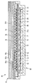
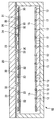
- FIG. 1 is a cross-sectional view illustrating a liquid crystal display device including a planar illumination device according to the first embodiment.
- FIG. 2A is a plan view showing a part of a support member in the planar illumination device
- FIG. 2B is a cross-sectional view taken along line AA ′ in FIG.
- FIG. 3 is a plan view showing a part of a transmission / reflection layer in the planar illumination device.
- FIG. 4 is an enlarged plan view showing a part of a support member according to a first modification.
- FIG. 5 is an enlarged plan view showing a part of a support member according to a second modification.
- FIG. 6 is a perspective view showing a support member according to the second modification.
- FIG. 1 is a cross-sectional view illustrating a liquid crystal display device including a planar illumination device according to the first embodiment.
- FIG. 2A is a plan view showing a part of a support member in the planar illumination device
- FIG. 2B is
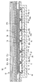
- FIG. 7 is a sectional view showing a liquid crystal display device provided with a planar illumination device according to the second embodiment of the present invention.
- FIG. 8 is a cross-sectional view showing a lower support member and a mounting board in the planar lighting device according to the second embodiment.
- FIG. 9 is a plan view and a cross-sectional view showing an upper support member in the planar illumination device according to the second embodiment.
- FIG. 10 is a cross-sectional view showing a support member according to a third modification.
- FIG. 11 is a cross-sectional view showing a support member according to a fourth modification.
- FIG. 12 is a cross-sectional view showing a support member according to a fifth modification.
- FIG. 13 is sectional drawing which shows the liquid crystal display device provided with the planar illuminating device which concerns on 3rd Embodiment.
- FIG. 14 is a cross-sectional view showing a liquid crystal display device provided with the planar illumination device according to the fourth embodiment.
- FIG. 15 is sectional drawing which shows the liquid crystal display device provided with the planar illuminating device which concerns on 5th Embodiment.
- FIG. 16 is a cross-sectional view illustrating a liquid crystal display device including the planar illumination device according to the sixth embodiment.
- FIG. 17 is a cross-sectional view illustrating a planar illumination device according to a seventh embodiment.
- FIG. 18 is a cross-sectional view illustrating a planar illumination device according to an eighth embodiment.
- FIG. 19 is a cross-sectional view showing a planar lighting device according to a ninth embodiment of the invention.
- FIG. 20 is a cross-sectional view showing a planar illumination device according to the tenth embodiment.
- FIG. 21 is a cross-sectional view illustrating a planar illumination device according to an eleventh embodiment.
- FIG. 22 is a sectional view showing a liquid crystal display device according to a twelfth embodiment.
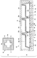
- FIG. 23 is a plan view and a sectional view showing a surface illumination device according to a thirteenth embodiment.
- FIG. 1 is a cross-sectional view of a liquid crystal display device provided with a planar illumination device according to the first embodiment of the present invention.
- the liquid crystal display device 90 includes a rectangular liquid crystal display panel 91, and a planar illumination device 92 as a backlight unit disposed facing the back side of the liquid crystal display panel 91.
- the liquid crystal display panel 91 includes a rectangular array substrate 91a, a rectangular counter substrate 91b arranged to face the array substrate 91a with a gap, and a liquid crystal layer 91c sealed between the array substrate and the counter substrate. I have.
- Each of the front and back surfaces of the liquid crystal display panel 91 is provided with a polarizing filter.
- the planar illumination device 92 is provided adjacent to and facing the array substrate 91 a of the liquid crystal display panel 91.
- the planar lighting device 92 has a size corresponding to the liquid crystal display panel 91, and includes a flat rectangular box-shaped frame 11 having an opening on the upper surface, and a plurality of members provided with the frame 11 as a base. Yes. That is, a plurality of mounting boards 17 are placed side by side on the bottom surface of the frame 11, and a plurality of light sources 12 made of, for example, LEDs are mounted on these mounting boards 17, and are placed side by side at intervals of, for example, 10 to 50 mm. Has been. In addition, a reflective sheet 15 having a thickness of 0.2 mm is disposed on the mounting substrate 17. These reflection sheets 15 are continuously arranged with each other except the portion of the light source 12. Thereby, the several light source 12 is provided in the planar radiation
- a lower spacer sheet 31 a made of an acrylic transparent sheet having a thickness of 0.3 mm formed in a bellows shape is placed as a sheet-like support member having light transmittance and a large number of irregularities. , Facing the light source 12.
- the peripheral edge portion of the lower spacer sheet 31 a is supported on the step portion of the frame 11.
- the light guide sheet 24 made of, for example, an acrylic transparent sheet having a thickness of 0.2 mm is disposed on the lower spacer sheet 31a, and is opposed to the reflective sheet 15 with a predetermined gap by the lower spacer sheet 31a. It is supported by.
- a transmission / reflection layer 25 is formed over substantially the entire top surface of the light guide sheet 24.
- An upper spacer sheet 31b made of an acrylic transparent sheet having a thickness of 0.3 mm, for example, formed in a bellows shape is placed on the transmission / reflection layer 25 as a sheet-like support member having optical transparency and a large number of irregularities. Yes.
- the upper spacer sheet 31b has the same structure as the lower spacer sheet 31a and is formed to have a slightly larger outer diameter than the lower spacer sheet 31a.
- the peripheral edge portion of the upper spacer sheet 31 b is supported on the peripheral edge portion of the frame 11.
- a rectangular diffusion sheet 16 having substantially the same size as the liquid crystal display panel 91 is disposed on the upper spacer sheet 31b, and is opposed to the light guide sheet 24 with a predetermined gap by the upper spacer sheet 31b. Is supported.
- a directivity improving sheet 18 and a polarization selective reflection sheet 19 are laminated in order.
- the diffusing sheet 16, the directivity improving sheet 18 and the polarization selective reflection sheet 19 constitute a planar radiation surface.
- optical sheets 18 and 19 above the diffusion sheet 16 have a configuration unique to the liquid crystal display device. When the lighting device is applied to a general lighting device, these optical sheets are omitted, and instead a thick diffusion plate. 16 can be used.
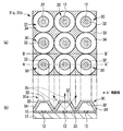
- FIG. 2A is an enlarged plan view showing a part of the lower spacer sheet 31a
- FIG. 2B is a view of the spacer sheet and the mounting substrate along the line AA ′ in FIG. It is sectional drawing.
- the lower spacer sheet 31a and the upper spacer sheet 31b have the same configuration.
- the lower spacer sheet 31a will be described as a representative.
- the lower spacer sheet 31a is a 0.3 mm acrylic transparent sheet that has been processed to be uneven according to the arrangement of the light sources 12 by vacuum molding.
- a plurality of frustoconical convex portions 30 are formed on a flat sheet, They are arranged vertically and horizontally.
- the lower spacer sheet 31a has a substantial volume of 50% or less with respect to the volume covered with the uneven surface.
- the lower spacer sheet 31a includes a flat contact region 33 on the lower side (reflection sheet 15 side), a plurality of flat contact regions 32 on the upper side (on the diffusion sheet 16 side), and a plurality of conical side regions connecting them. 34.
- the upper contact region 32 is formed by the upper surface of each convex portion 30.
- the side surface region 34 is inclined so that the light beam 35 emitted from the light source 12 approaches vertical incidence, and has a substantially circular curved boundary portion when viewed from above so as to have sufficient strength against the force applied from above and below.
- the side regions 34 are formed at a light source array interval (10 to 50 mm), and each have a function corresponding to a support column.
- the lower spacer sheet 31 a is disposed such that the contact region 33 is in contact with the reflection sheet 15 and the plurality of convex portions 30 are coaxially overlapped with the light source 12.
- the upper spacer sheet 31b having the same configuration is arranged such that the convex portions 31 are coaxially overlapped with the convex portions 30 of the lower spacer sheet 31a.
- the spacer sheet 31a and the upper spacer sheet 31b since the interval in which the columns, that is, the side regions 34 are arranged is extremely narrow (10 to 50 mm) as compared with the prior art, the adjacently stacked members (light guides) Even if the sheet 24 and the diffusion sheet 16) are thin, these members can be supported stably without causing positional shift due to bending.
- the intervals between the protrusions 30 serving as support columns are uniform and high in density, uniform strength can be ensured over the entire spacer sheet without worrying about the installation position of the spacer sheet against pressure from above and below. . For the same reason, even if a lighting device with a curved surface is configured, the spacer sheet can support gaps uniformly across the entire surface and ensure the strength.
- the lower and upper spacer sheets 31a and 31b are made of transparent and uniform sheets, there is basically no refraction and concentration due to absorption or prism action. Therefore, the lower and upper spacer sheets 31a and 31b themselves have a small optical influence, and the luminance distribution change due to the spacer sheet itself is very small.
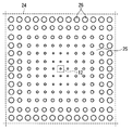
- FIG. 3 shows an opening pattern of the transmissive reflection layer 25 formed on the light guide sheet 24.
- the transmission / reflection layer 25 is formed on the light guide sheet 24 by a printing process using a printing paste containing particles to be reflected and scattered.
- the transmission / reflection layer 25 includes a transmission part having a plurality of transmission holes 26 formed in a predetermined opening pattern so as to give a predetermined transmittance distribution, and a reflection part that reflects a part of the light.
- the transmission / reflection layer 25 is formed so that the transmission ratio of light in the upper part (center part) of the light source 12 is smaller than that in the part (end part) away from the light source 12.
- the transmission / reflection layer 25 is adjusted so as to strongly reflect the strong light on the upper part of the LED 12 and make the luminance of the planar illumination device 10 uniform as a whole.
- the transmission / reflection layer 25 was printed on a plate-like member in the prior art, it was cut after being set in the printing device one by one, but in the configuration of the present embodiment, the light guide sheet 24 became thin, A roll-like sheet can be handled and formed at a time from printing to cutting in a roll-to-roll process. Further, the uneven shape and material of the spacer sheet 31 can be arbitrarily changed according to the required performance.
- an optical member that has at least one function of diffusion, refraction, and reflection and faces the planar radiation surface here
- the light guide sheet 24, the transmission / reflection layer 25, and the diffusion sheet 16 are supported by the lower spacer sheet 31a and the upper spacer sheet 31b having light transmittance and a plurality of irregularities, respectively, so that the optical member is thinned. Even if they are formed, they can be stably supported without displacement. Thereby, an optical member and a structural member can be formed thinly, and the weight of an illuminating device can be reduced.
- the weight of the resin component in the conventional configuration is 5 kg, but in this embodiment, the weight is reduced to less than 2 kg.
- the structure and assembly of the lighting device can be simplified. Since the interval between the constituent members is ensured by the light source arrangement interval, it is possible to design a uniform strength over the entire surface of the planar illumination device, and it can also be applied to an illumination device having a curved surface. From the above, it is possible to provide a planar lighting device that is lightweight and has high strength and can be thinned, and a liquid crystal display device including the planar lighting device.
- 0.3 mm thick sheets are used as the spacer sheets 31a and 31b that function as sheet-like support members.
- the thickness of the sheets may be increased.
- seat with uniform board thickness was formed by vacuum forming, when forming by injection molding etc., it is good also as a spacer sheet
- the diffusion sheet 16 may be a diffusion plate having a thickness.
- the pressure received can be dispersed over a wide range due to the rigidity of the diffusion plate, and the strength of the lighting device can be ensured by using a thinner spacer sheet. it can.
- the light guide sheet 24 on which the transmissive reflection layer 25 is formed can also reduce the production cost.
- the material of the lower and upper spacer sheets 31a and 31b is an acrylic transparent sheet.
- the material may be selected in consideration of not only the transmittance but also the heat resistance and moisture resistance.
- a sheet may be used.
- vacuum forming that can be manufactured at low cost is used as a manufacturing method of the spacer sheet 31.
- a sheet having unevenness may be manufactured by other manufacturing methods such as injection molding or extrusion molding.
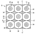
- FIG. 4 shows an enlarged part of the spacer sheet 31 according to the first modification.
- circular protrusions 38 are provided between the plurality of convex portions 30 for the purpose of alleviating the bending strength deterioration in the BB ′ section of the spacer sheet 31b shown in FIG. Yes.
- the bending strength is improved by the bellows structure even in the B-B ′ cross section, and the handling property and the yield of the spacer sheet during assembly are improved.
- a substantially circular protrusion is used here, the same effect may be obtained by a linear rib, and the arrangement interval of the protrusions is not matched with the light source 12, and may be finer or rougher than the light source arrangement.
- FIG. 5 shows an enlarged part of the spacer sheet 31 according to the second modification.
- the spacer sheet 31 according to the second modification is configured so as not to have a bellows structure in the B-B ′ section extending between the adjacent protrusions 30, and is easily bent in the same section. That is, the spacer sheet 31 has a bending moment that is extremely small in the cross section formed by a predetermined straight line or closed curve as compared with other cross sections.
- Such a configuration is effective in a lighting device formed in a cylindrical curved surface as shown in FIG. 6, and the spacer sheet 31 is bent along a predetermined straight line or a closed curved surface.
- a region having a low bending moment is arranged in a circle, it can be used for a lighting device formed in a spherical curved surface.
- FIG. 7 is a cross-sectional view of a liquid crystal display device provided with a planar illumination device according to the second embodiment
- FIG. 8 is a cross-sectional view of a lower spacer sheet
- FIGS. 9 (a) and 9 (b) are upper views. It is the top view and sectional drawing of a spacer sheet.
- the other configurations of the liquid crystal display device are the same as those of the first embodiment described above, and different parts will be described in detail. The same reference numerals as those of the embodiment are attached and detailed description thereof is omitted.
- the lower spacer sheet 31a has the same shape as that of the first embodiment, but is not a transparent sheet but an opaque sheet including diffusing particles 36.
- the diffusion particles 36 are particles having a refractive index of about 10 ⁇ m which are different from those of the acrylic base material, and are mixed in the acrylic base material.
- the mean free path of scattering of the diffusing particles 36 is adjusted to about 0.002 to 0.2 mm, and the transmittance of the 0.3 mm thick sheet is set to about 50 to 90%. Thereby, the light beam 35 emitted from the light source 12 is scattered to the periphery by the lower spacer sheet 31a, and the burden on the transmission / reflection layer 25 is reduced.
- the upper spacer sheet 31b is provided with a plurality of rib-shaped protrusions 30 extending in the same direction on an acrylic transparent sheet having a thickness of 0.3 mm.
- the inclination accuracy of each convex portion 30 is made uniform at about 20 to 70 degrees, the height is set to 1 to 4 mm, and the interval between the convex portions is set to about 1 to 4 mm.
- the upper spacer sheet 31b having a uniform thickness does not collect light due to the prism action, and thus uneven brightness does not occur.
- the upper spacer sheet 31b has a configuration in which the side region 34 having a uniform inclination angle is increased as much as possible and the upper and lower plane regions are reduced as much as possible. Therefore, the reflectance does not change depending on the angle of incidence on the upper spacer sheet 31b, and the difference in reflectance due to the inclination of the convex portion 30 is eliminated between the side surface region and the upper and lower planar regions, and luminance unevenness between both regions is eliminated. Can be reduced. Further, the pitch of the unevenness is made as fine as about 4 mm so as to make it inconspicuous by the diffusion sheet 16 or the like.
- the reason why the upper spacer sheet 31b is configured as a ridge is to increase the number of rays incident on the spacer sheet 31b in the vicinity of the Brewster angle and effectively use it on the front liquid crystal display panel 91 in addition to the purpose of increasing the side surface of the uniform inclination angle described above. This is to increase the light emitted.
- light rays emitted from the lower light guide sheet 24 are directed in various directions, the vertical direction of the light guide sheet 24 is mainly strongest.
- the light beam 35 emitted in the front is easily reflected by the spacer sheet 31b in parallel with the parallel light, and easily transmitted by the vertical polarized light.
- the reflected parallel polarized light is reflected back to the back surface again, and returns with a vertical polarization component.
- This effect is not as effective as the polarization selective reflection sheet 19 because the light emitted from the light guide sheet 24 has various directions, and the polarization is slightly disturbed by the diffusion sheet 16, but it causes a large loss.
- the light emitted from the backlight unit can be polarized. Thereby, the ratio of the light beam reflected by the polarization selective reflection sheet can be reduced, and a liquid crystal display device with improved light utilization efficiency can be realized.
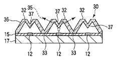
- the lower spacer sheet 31a may be configured by coating the surface of a transparent sheet with diffusion particles 36 as in the third modification shown in FIG. Further, the surface of the transparent sheet may be subjected to fine uneven processing to disperse the refraction angle. In either case, light can be scattered by the spacer sheet 31a to reduce the burden on the transmission / reflection layer 25. Further, the scattering particle coating or surface treatment may be performed on one side or both sides of the spacer sheet.
- a small concave portion 37 is provided in the contact region 32 of each convex portion 30 facing the light source 12, and just above the light source 12. It may be arranged.
- the concave portion 37 can increase the incident angle of light on the lower spacer sheet 31 a by its shape itself, and has an effect of dispersing a strong light beam emitted directly above the light source 12 by increasing a reflection component.
- the concave portion 37 is strong enough to increase the path length through which the light beam traveling directly above the light source 12 passes through the lower spacer sheet 31a. As a result, the burden on the transmission / reflection layer 25 can be reduced.
- FIG. 13 is a cross-sectional view of a liquid crystal display device including the planar illumination device according to the third embodiment.
- the third embodiment except for the configuration of the spacer sheet, other configurations of the liquid crystal display device are the same as those of the first embodiment described above, and different parts will be described in detail. The same reference numerals as those of the embodiment are attached and detailed description thereof is omitted.
- the light guide sheet 24 on which the transmission / reflection layer 25 is formed is formed so as to also function as the spacer sheet 31.
- the configuration and principle other than the light guide sheet 24 that also serves as the spacer sheet 31 are the same as those in the first embodiment.
- the light guide sheet 24 has a plurality of protrusions 30a that protrude toward the reflection sheet 15 and a plurality of protrusions 30b that protrude toward the diffusion sheet 16, respectively. These convex portions 30a and 30b are provided so as to face a portion between the adjacent light sources 12 where the aperture ratio of the transmission / reflection layer 25 is high and the aperture ratio changes gently.
- the bottom surface of each convex portion 30 a forms a lower contact region 33 and is in contact with the reflection sheet 15.
- the upper surface of the upper convex portion 30 b forms a contact region 32 and is in contact with the diffusion sheet 16.
- the diffusion sheet 16 is supported by the light guide sheet 24 serving also as the spacer sheet so as to face the reflection sheet 15 with a predetermined interval.
- the number of sheets to be stacked can be reduced, and the lighting device can be further reduced in weight and thickness.
- the effect similar to 1st Embodiment can be acquired.
- the spacer sheet formation part of the light guide sheet 24, ie, a convex part, is provided in the upper and lower surfaces of the light guide sheet 24, it is not restricted to this, It is good also as a structure provided only in the single side
- FIG. 14 is a cross-sectional view of a liquid crystal display device including the planar illumination device according to the fourth embodiment.
- the spacer sheet 31 has a bellows configuration with an uneven height of about 50 mm.
- the unevenness arrangement interval of the spacer sheet 31 corresponds to the arrangement pitch of the light sources 12.
- the spacer sheet 31 is placed on the reflection sheet 15, and a thin diffusion sheet 16 is supported on the spacer sheet 31. Thick diffusers and struts are eliminated.
- the transmission / reflection layer is not used, and the spacer sheet 31 as a support member is configured to support the diffusion sheet 16.
- FIG. 15 is a cross-sectional view of a liquid crystal display device including the planar illumination device according to the fifth embodiment.
- the uneven arrangement interval of the spacer sheet 31 is twice the arrangement pitch of the light sources 12. Thereby, the aspect ratio of the diaphragm at the time of vacuum forming of the spacer sheet 31 is halved, and the conditions under which the spacer sheet can be formed can be widened.
- FIG. 16 is a cross-sectional view of a liquid crystal display device including the planar illumination device according to the sixth embodiment.
- the spacer sheet 31 c having a large number of irregularities and the flat spacer sheet 31 d are disposed between the reflection sheet 15 and the diffusion sheet 16 so as to overlap each other. Thereby, the height of the unevenness
- seat 31c is made low, and the amount of drawing at the time of vacuum forming is reduced.
- the other configurations of the liquid crystal display device are the same as those of the first embodiment, and the same reference numerals as those of the first embodiment are given to the same portions. A detailed description thereof will be omitted.
- FIG. 17 is a cross-sectional view of the planar illumination device according to the seventh embodiment.
- the planar illumination device 92 includes a flat box-shaped frame 11 having an open top surface and a plurality of members provided with the frame 11 as a base. That is, a plurality of mounting boards 17 are placed side by side on the bottom surface of the frame 11, and a plurality of light sources 12 made of, for example, LEDs are mounted on these mounting boards 17, and are placed side by side at intervals of, for example, 10 to 50 mm. Has been.
- a reflective sheet 15 having a thickness of 0.2 mm is disposed on the mounting substrate 17.
- reflection sheets 15 are continuously arranged with each other except the portion of the light source 12. Thereby, the several light source 12 is provided in the planar radiation
- the mounting substrate 17 is divided into a plurality of parts, the present invention is not limited to this, and the mounting board 17 may be composed of a single piece.
- a rectangular diffusion plate 20 is disposed so as to close the upper opening of the frame 11 and is supported on the peripheral edge of the frame 11.
- the diffusion plate 20 faces the light source 12 and the reflection sheet 15 substantially in parallel with a gap.
- the diffusion plate 20 constitutes a planar radiation surface, and here, a flat rectangular radiation surface.
- a rectangular light guide sheet 24 made of, for example, an acrylic transparent sheet having a thickness of 0.2 mm is disposed between the reflection sheet 15 and the diffusion plate 20 and faces the reflection sheet 15 with a gap.
- a transmission / reflection layer 25 is formed over substantially the entire upper surface of the light guide sheet 24, that is, the surface on the diffusion plate 20 side.
- a spacer sheet 31 made of an acrylic transparent sheet having a thickness of 0.3 mm formed in a bellows shape. Is arranged.
- the spacer sheet 31 has a large number of protrusions 30 protruding toward the light guide sheet 24, and contact areas 32 formed by the upper surfaces of the protrusions 30 are fixed to the light guide sheet 24. Further, the contact regions 33 on the diffusion plate 30 side of the spacer sheet 31 are respectively fixed to the diffusion plate 30.
- the peripheral edge of the spacer sheet 31 is supported by the frame 11. Thereby, the light guide sheet 24 is supported by the spacer sheet 31 so as to face the diffusion plate with a predetermined gap.
- the lighting device 92 has a size of 500 mm or less, which is not required to be as large as the backlight unit, but rather has a strong demand for thinning.
- a light guide sheet 24 on which a transmission / reflection layer 25 for thinning is formed is provided, and a spacer sheet 31 is used as a member for supporting the light guide sheet 24.
- the spacer sheet 31, the light guide sheet 24, and the diffusion plate 20 are bonded and fixed to each other with a transparent adhesive, and the light guide sheet 24 is supported by the spacer sheet 31 at a predetermined interval.
- FIG. 18 is a cross-sectional view of the planar illumination device according to the eighth embodiment.
- the spacer sheet 31 is formed by the light guide sheet 24, and the light guide sheet has a support function. That is, the light guide sheet 24 has a large number of protrusions 30 protruding toward the diffusion plate 20, and a contact region 32 formed by the upper surface of each protrusion is fixed to the diffusion plate 20. According to such a configuration, the number of optical sheets can be reduced, and the configuration of the lighting device can be simplified and further thinned.
- FIG. 19 is a cross-sectional view of a planar illumination device according to the ninth embodiment.
- the spacer sheet 31 is disposed between the light guide sheet 24 and the reflection sheet 15, and is bonded and fixed to the light guide sheet 24 and the reflection sheet 15.
- the light guide sheet 24 is supported by the spacer sheet 31 with a predetermined distance from the light source 12. Even in such a configuration, the same effects as those of the seventh embodiment can be obtained.
- FIG. 20 is a cross-sectional view of the planar illumination device according to the tenth embodiment.
- the light guide sheet 24 having the function of the spacer sheet 31 on the light guide sheet 24 and having the transmission / reflection layer 25 formed on the surface thereof is disposed on the light source 12 side, that is, on the reflection sheet 15. I support it.
- a sparse light source illuminating device in which LED chips are aggregated is shown, but in the illuminating device having such a configuration, the original diffusion plate 20 has a certain degree of rigidity. Therefore, it is more important for the spacer sheet 31 to appropriately position the transmission / reflection layer 25 for thickness reduction than the function of supporting the diffusion member.
- the structure in which the light guide sheet 24 that also serves as the sheet-like spacer sheet 31 is placed on the base material of the light source 12 can realize a reduction in thickness and increase productivity.
- FIG. 21 is a cross-sectional view of the planar illumination device according to the eleventh embodiment.
- the spacer sheet 31 that also serves as the transmission / reflection layer 25 may have a function of supporting the diffusion plate 20, and the diffusion plate may be thinned by supporting the spacer sheet 31.
- the base material on the light source 12 side, here, the reflection sheet 15 is not limited to be flat, but as shown in FIG. 21, the spacer sheet 31 is installed on the reflection sheet 15 formed in an uneven shape. Also good.
- FIG. 22 is a cross-sectional view of a liquid crystal display device including the planar illumination device according to the twelfth embodiment.
- the planar illumination device 92 is placed on the reflection sheet 15 and is placed on the lower spacer sheet (support member) 31a that also serves as the transmission / reflection layer 25, and on the lower spacer sheet 31a.
- the upper spacer sheet (support member) 31b is provided, and the diffusion sheet 16 is supported by the upper spacer sheet 31b.
- a directivity improving sheet 18 and a polarization selective reflection sheet 19 are laminated in order.
- the diffusing sheet 16, the directivity improving sheet 18 and the polarization selective reflection sheet 19 constitute a planar radiation surface.
- the upper spacer sheet 31b is the same as the upper spacer sheet in the second embodiment shown in FIG.
- the liquid crystal display device 90 is configured to adjust the lighting brightness by dividing the individual light sources 12 into a plurality of groups according to the display image.
- the lower spacer sheet 31a has a plurality of regions that protrude toward the reflecting sheet 15a, and these regions constitute side walls 31d that divide the group according to the group of the light sources 12 that are collectively adjusted.
- the transmission / reflection layer 25 has a region 25a that faces each normal light source 12 to make the light luminance uniform, and a region 25b that shields between groups of the light sources 12 that adjust the lighting luminance.
- the region 25b is formed on the surface of the side wall 31d and functions to suppress and control light leaking from the adjacent lighting luminance region. Thereby, in the liquid crystal display device that adjusts the lighting luminance by dividing the light source 12 into groups, a luminance profile for each desired region can be formed.
- the other configuration of the liquid crystal display device is the same as that of the above-described second embodiment, and the same portions are denoted by the same reference numerals and detailed description thereof is omitted.
- FIG. 23A is a plan view of a planar illumination device according to the thirteenth embodiment
- FIG. 23B is a cross-sectional view taken along line EE of FIG.
- This embodiment is an illumination device that constitutes a two-color bulletin board.
- This illuminating device does not display a pattern with a conventional color selective absorption filter, but displays two-color patterns 16a and 16b with transmission and reflection layers 25a and 25b formed on a spacer sheet 31 as a support member.
- the surface diffusing plate 16 forming the planar radiation surface does not use any color selective absorption filter.
- the spacer sheet 31 has a plurality of projections and depressions, is placed on the reflection sheet 15, and supports the diffusion plate 16 provided facing the light sources 12a and 12b.
- the unevenness of the spacer sheet 31 has a delimiter portion 31c formed along the color boundary in accordance with the symbols 16a and 16b, and a high-shielding transmission / reflection layer 25b is formed on the delimiter portion 31c.
- a transmission / reflection layer 25a is formed to make the light luminance uniform.
- the transmission / reflection layers 25a and 25b are also formed on the surface of the spacer sheet 31 on the diffusion plate 16 side.
- two types of light sources 12a and 12b having different wavelengths to be emitted are provided, one light source 12b is disposed in a region facing the region surrounded by the transmission / reflection layer 25b, and the other light source 12a is disposed. It arrange
- the transmission / reflection layer 25b suppresses light leakage between these areas, and displays the desired symbols 16a and 16b. Thereby, it is possible to provide a simpler and power-saving bulletin board illumination device.
- the other configuration of the lighting apparatus is the same as that of the second embodiment described above, and the same reference numerals are given to the same portions, and detailed description thereof is omitted.
- the present invention is not limited to the above-described embodiment as it is, and can be embodied by modifying the constituent elements without departing from the scope of the invention in the implementation stage.
- various inventions can be formed by appropriately combining a plurality of components disclosed in the embodiment. For example, some components may be deleted from all the components shown in the embodiment.
- constituent elements over different embodiments may be appropriately combined.
- the LED as the point light source may be white or monochromatic, and the type of LED is not limited.
Landscapes
- Physics & Mathematics (AREA)
- General Physics & Mathematics (AREA)
- Optics & Photonics (AREA)
- Nonlinear Science (AREA)
- Mathematical Physics (AREA)
- Chemical & Material Sciences (AREA)
- Crystallography & Structural Chemistry (AREA)
- Liquid Crystal (AREA)
- Planar Illumination Modules (AREA)
- Optical Elements Other Than Lenses (AREA)
Abstract
照明装置は、複数の光源12と、拡散、屈折、反射の少なくとも1つの光学特性を有し、前記光源に対向する光学部材24と、複数の凹凸を有し、前記光学部材を支持する光透過性を有したシート状の支持部材31aと、を備える。
Description
本発明の実施形態は、発光面の直下に配置された光源とその光源像を拡散させる拡散部材とを備え、平面あるいは曲面で発光させる面状照明装置、およびこれを用いた液晶表示装置に関する。
面状照明装置は、光源から出た光を面状の発光面から放射する装置である。このような面状照明装置は、それ自体で照明装置として使用される他に、液晶表示パネルと組合わせて液晶表示装置にも使われている。
照明装置の構造としては、発光ダイオード(LED)や冷陰極管(CCFL)などの光源を面状の発光面の直下に面状に配置した直下型と、光源を板状の導光体の側面に配置したサイド型とがある。直下型は光利用効率に優れていて主に照明用途として用いられ、サイド型は薄さに優れていて主に中小型の液晶表示装置のバックライトユニットとして用いられている。また、バックライトユニットであっても大型で高画質・省電力を要求されるものについては、直下型の照明装置が用いられている。
このようなバックライトユニットでは、光源にLEDを用いて、個々のLEDあるいは複数のLEDグループ毎に、画像に合わせて光量を調光して出力するローカルディミング技術を搭載している。これにより、漏れ光による黒表示劣化を抑制し、また、消費電力を抑制することが可能となる。
上記のようなサイド型の照明装置では、光利用効率と重量に問題があった。光利用効率は、導光される光線の経路が長く複雑化するほど途中で吸収される光損失が増大するために発生する。これは製品の光量不足、光源コストの増大、発熱構造の複雑化を招く。重量は、主に導光板の厚さに依存するが、薄くすると上述した光利用効率が劣化していくため現状では4mm程度の厚さが主流となっている。50インチクラスでは、導光板だけで4kg程度に達するため、強度を確保するための構造が複雑長大になるほか、装置重量、材料コストに問題を招いている。
直下型の照明装置では、サイド型のような光利用効率の問題は改善されているが、厚板の拡散板を用いるために重量の問題は残っている。また、照明装置自体が厚くなること、支柱を設置することによる組立複雑化や強度信頼性の劣化といった新たな問題を招いていた。
厚さを改良した直下型の照明装置においても、導光板と光源の接触によるLEDの破壊を避ける必要から導光板は光源から離して設置する必要がある。透過反射層の位置も離れたり近すぎたりすると輝度補償量が変動して輝度ムラを生じるため、厳密に位置を規定する必要があった。このため、導光板を剛性のある厚い板部材として、支柱により導光板を支持固定する構造となり、重量増大や組立複雑化を招いていた。
別の薄型化技術として、LED光源の上に配光を広げるレンズを設置し、これにより光源と拡散板の隙間を縮小させる技術が提案されている。しかしながら、このような構成では個々の光源にレンズを設置する必要が生じ、組立複雑化を招いてしまう。
この発明は以上の点を鑑みて直下型の照明装置に対してなされたものであり、その目的は新たな支持手段により、第一に照明装置の重量とこれに係わる問題を軽減すること、第二に照明装置の組立を簡略化するとともに強度に係る問題を軽減すること、第三に光学的な補助手段を提供して用途に応じた特性向上を付与することであり、液晶表示装置分野においては壁掛けTVにつながる軽量高強度バックライトユニットを、照明分野においては床面あるいは机上で使える薄型高強度の面状照明装置を可能とする技術を提供することにある。
この発明の態様に係る照明装置は、複数の光源と、拡散、屈折、反射の少なくとも1つの光学特性を有し、前記光源に対向する光学部材と、複数の凹凸を有し、前記光学部材を支持する光透過性を有したシート状の支持部材と、を備えている。
この発明の態様に係る液晶表示装置は、液晶表示パネルと、前記液晶表示パネルに対向して配置され、前記液晶表示パネルに光を照射する前記照明装置と、を備えている。
以下、図面を参照しながら、この発明の実施形態に係る面状照明装置を備えた液晶表示装置について詳細に説明する。なお、実施形態では、面状照明装置を液晶表示装置のバックライトユニットとして用いる構成を説明しているが、面状照明装置のみを照明装置として利用することもできる。
図1は、この発明の第1の実施形態に係る面状照明装置を備えた液晶表示装置の断面図である。図1に示すように、液晶表示装置90は、矩形状の液晶表示パネル91、およびこの液晶表示パネル91の背面側に対向して配設されたバックライトユニットとしての面状照明装置92を備えている。液晶表示パネル91は、矩形状のアレイ基板91a、アレイ基板91aと隙間を置いて対向配置された矩形状の対向基板91b、およびこれらアレイ基板と対向基板との間に封入された液晶層91cを備えている。液晶表示パネル91の前面および裏面は、それぞれ偏光フィルタが設けられている。面状照明装置92は、液晶表示パネル91のアレイ基板91aと隣接対向して設けられている。
面状照明装置92は、液晶表示パネル91に対応する大きさを有し、上面の開口した偏平な矩形箱状のフレーム11と、このフレーム11を土台として設けられた複数の部材とを備えている。すなわち、フレーム11の底面上に、複数の実装基板17が並べて載置され、これらの実装基板17上に、例えば、LEDからなる複数の光源12が実装され、例えば、10~50mm間隔で並べて配置されている。また、実装基板17上に0.2mm厚さの反射シート15が配置されている。これらの反射シート15は、光源12の部分を除き、互いに連続して並べられている。これにより、複数の光源12は、面状の放射面に設けられている。なお、実装基板17は複数に分割されているが、これに限らず、1枚で構成してもよい。
反射シート15の上に、光透過性および多数の凹凸を有するシート状の支持部材として、例えば、蛇腹状に形成した厚さ0.3mmのアクリル透明シートからなる下側スペーサシート31aが載置され、光源12と対向している。下側スペーサシート31aの周縁部は、フレーム11の段部上に支持されている。下側スペーサシート31aの上に、例えば、厚さ0.2mmのアクリル透明シートからなる導光シート24が配置され、下側スペーサシート31aにより、反射シート15と所定の隙間を置いて対向する状態に支持されている。導光シート24の上面のほぼ全体に亘って、透過反射層25が形成されている。
透過反射層25上に、光透過性および多数の凹凸を有するシート状の支持部材として、例えば、蛇腹状に形成した厚さ0.3mmのアクリル透明シートからなる上側スペーサシート31bが載置されている。この上側スペーサシート31bは、下側スペーサシート31aと同一の構造を有し、下側スペーサシート31aよりも僅かに大きな外径に形成されている。上側スペーサシート31bの周縁部は、フレーム11の周縁部上に支持されている。
更に、上側スペーサシート31bの上に、液晶表示パネル91とほぼ同一の大きさを有する矩形状の拡散シート16が配置され、上側スペーサシート31bにより、導光シート24と所定の隙間を置いて対向した状態に支持されている。拡散シート16の上に指向性向上シート18および偏光選択反射シート19が順に積層されている。これら拡散シート16、指向性向上シート18および偏光選択反射シート19により、面状の放射面を構成している。
これらの光学部材は、図示しない周辺部の固定構造で積層支持されており、照明領域に支柱を配置することも可能であるが、従来のような多数配置は不要としている。なお、拡散シート16より上の光学シート類18、19は液晶表示装置特有の構成であり、照明装置を一般の照明装置の適用する場合は、これらの光学シートを省略し、代りに厚い拡散板16を用いることができる。
図2(a)は、下側スペーサシート31aの一部を拡大して示す平面図、図2(b)は、図2(a)の線A-A‘に沿ったスペーサシートおよび実装基板の断面図である。
下側スペーサシート31aおよび上側スペーサシート31bは同一の構成を有し、ここでは、下側スペーサシート31aを代表して説明する。下側スペーサシート31aは、0.3mmのアクリル透明シートを真空成型により光源12の配列にあわせて凸凹加工したもので、平坦なシートに、例えば、それぞれ切頭円錐形状の凸部30を複数、縦横に並べて形成している。下側スペーサシート31aは、凸凹面で外装される体積に対して、実質的な体積が50%以下に形成されている。
下側スペーサシート31aおよび上側スペーサシート31bは同一の構成を有し、ここでは、下側スペーサシート31aを代表して説明する。下側スペーサシート31aは、0.3mmのアクリル透明シートを真空成型により光源12の配列にあわせて凸凹加工したもので、平坦なシートに、例えば、それぞれ切頭円錐形状の凸部30を複数、縦横に並べて形成している。下側スペーサシート31aは、凸凹面で外装される体積に対して、実質的な体積が50%以下に形成されている。
下側スペーサシート31aは、下側(反射シート15側)の平坦な接触領域33と、上側(拡散シート16側)の複数の平坦な接触領域32と、これらをつなぐ複数の円錐状の側面領域34とを有している。上側の接触領域32は、各凸部30の上面により形成されている。側面領域34は、光源12から放射される光線35が垂直入射に近づくように傾斜させるとともに、上下から加わる力に対して十分な強度を有するように上から見て略円状の曲面境界部を有している。この側面領域34は光源配列間隔(10~50mm)で形成され、それぞれ支柱に相当する機能を有している。そして、下側スペーサシート31aは、接触領域33が反射シート15上に接触し、複数の凸部30がそれぞれ光源12と同軸に重なるように配置されている。同様の構成を有する上側スペーサシート31bは、それぞれ凸部31が、下側スペーサシート31aの凸部30と同軸的に重なるように、配置されている。
下側スペーサシート31aおよび上側スペーサシート31bは、従来技術に比べて支柱、すなわち側面領域34の配列される間隔が極端に狭くなるため(10~50mm)、隣接して積層される部材(導光シート24、拡散シート16)が薄くても、これらの部材に撓みによる位置のずれを生じさせることなく、安定して支持することができる。また、支柱となる凸部30間隔が均一で高密度となるため、上下からの圧力に対してスペーサシートの設置位置を気にすることなく、スペーサシート全面で均一な強度を保障することができる。また、同様の理由により、曲面を付与した照明装置を構成しても、スペーサシートにより、全面均一な隙間支持と強度保障が可能である。また、下側および上側スペーサシート31a、31bは、透明で均一厚さのシートにより構成しているため、基本的に吸収やプリズム作用による屈折集光がない。そのため、下側および上側スペーサシート31a、31b自体は光学的な影響が小さく、スペーサシート自体による輝度分布変化は非常に小さい。
図3は、導光シート24上に形成された透過反射層25の開口パターンを示している。透過反射層25は、反射散乱させる粒子を含んだ印刷ペーストを用いて印刷プロセスにより導光シート24上に形成されている。透過反射層25は、所定の透過率分布を付与すべく所定の開口パターンで形成された複数の透過孔26を有する透過部と、光の一部を反射する反射部とを有している。ここでは、透過反射層25は、光源12から離れた部分(端部)に比べ光源12の上部(中央部)の光の透過割合が小さくなるように形成されている。すなわち、透過反射層25において、LED12から離れた部分(端部)に比べLED12の上部(中央部)の透過孔26の孔径が小さく形成されている。これにより、透過反射層25は、LED12の上部の強い光を強く反射して、全体として面状照明装置10の輝度を均一にするように調整されている。
透過反射層25は、従来技術では板状部材に印刷していたため、1枚毎に印刷装置にセットした後に裁断していたが、本実施形態の構成では、導光シート24が薄くなったため、ロールツーロールプロセスにて印刷から裁断までロール状のシートをハンドリングして一度に形成することが可能となる。また、スペーサシート31の凸凹形状や材質は、要求性能にあわせて任意に変更可能である。
上記のように構成された面状照明装置92を備えた液晶表示装置90によれば、少なくとも拡散、屈折、反射の少なくとも1つの機能を有し面状の放射面に対向した光学部材、ここでは、導光シート24、透過反射層25、および、拡散シート16をそれぞれ光透過性および複数の凹凸を有する下側スペーサシート31aおよび上側スペーサシート31bで支持する構成とすることにより、光学部材を薄く形成しても、これらを位置ずれなく安定して支持することができる。これにより、光学部材、および構成部材を薄く形成し、照明装置の重量を軽量化することができる。50インチクラスの液晶表示パネルに適用したバックライトユニットの実施形態では、従来構成で樹脂部品重量が5kgであったものが、本実施形態では、2kg弱に軽量化される。また、上記構成によれば、構成部材を順次積層配置して周辺を位置合わせ固定するだけでよく、従来のような独立した多数の支柱を位置決め配置する必要がない。そのため、照明装置の構造および組立を簡略化することができる。構成部材同士の間隔は光源配列間隔で確保されているため、面状照明装置の全面に渡って均一な強度設計が可能であり、曲面を有する照明装置へも適用することができる。以上のことから、軽量で高強度を有するとともに、薄型化が可能な面状照明装置、およびこれを備えた液晶表示装置を提供することができる。
本実施形態では、シート状の支持部材として機能するスペーサシート31a、31bとして0.3mm厚のシートを用いたが、高い強度が求められる場合はシートの厚さをより厚くしてもよい。また、真空成型により板厚が均一なスペーサシートを形成したが、射出成型などで形成する場合は、不均一な板厚を有するスペーサシートとしてもよい。蛇腹状の構造により本来100%充填した場合の体積を、凹凸の部分で空気に置き換えて軽量化することが重要であり、凸凹による隙間は本来充填される空間の50%以上を確保すれば十分な軽量化がなされる。
拡散シート16は、板厚の拡散板としてもよく、この場合、拡散板の剛性により、受ける圧力を広範囲に分散させることができ、より薄いスペーサシートを用いて照明装置の強度を確保することができる。また、この場合、透過反射層25を形成した導光シート24も生産コストを下げることができる。
本実施形態では下側および上側スペーサシート31a、31bの材料をアクリル透明シートとしたが、材料は透過率だけでなく、耐熱性、耐湿性を考慮して適時選択すればよく、複合シートやコーティングシートを用いてもよい。また、本実施形態ではスペーサシート31の製造手法として、安価で製造できる真空成型を用いたが、射出成型や押し出し成型などで他の製造手法により、凹凸を有するシートを製造してもよい。
図4は、第1変形例に係るスペーサシート31の一部を拡大して示している。第1変形例に係るスペーサシート31では、図2に示すスペーサシート31bのB-B‘断面における曲げ強度劣化を緩和する目的で、複数の凸部30間に、円形の突起38が付与されている。これによりB-B’断面においても蛇腹構造による曲げ強度向上がなされ、組立時のスペーサシートのハンドリング性や歩留りが向上する。ここでは略円形の突起としたが、同様の効果は直線状のリブでもよく、突起の配列間隔も光源12に合わせることはなく、光源配列より細かくても荒くてもよい。
図5は、第2変形例に係るスペーサシート31の一部を拡大して示している。第2変形例に係るスペーサシート31は、隣り合う凸部30間を延びるB-B‘断面で蛇腹構造をとらないように構成され、同断面にて曲げ易く形成されている。すなわち、スペーサシート31は、所定の直線あるいは閉曲線で形成される断面において、その他の断面よりも極端に曲げモーメントが小さく形成されている。このような構成は、図6に示すような円筒曲面に形成した照明装置で有効であり、スペーサシート31は、所定の直線あるいは閉曲面で曲げられている。同様に、曲げモーメントの低い領域を円形に配置すれば球面曲面に形成した照明装置に用いることができる。
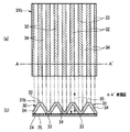
次に、第2の実施形態に係る液晶表示装置について説明する。図7は、第2の実施形態に係る面状照明装置を備えた液晶表示装置の断面図、図8は、下側スペーサシートの断面図、図9(a)、9(b)は、上側スペーサシートの平面図および断面図である。第2の実施形態において、スペーサシートの構成を除いて、液晶表示装置の他の構成は前述した第1の実施形態と同一であり、異なる部分を詳細に説明し、同一の部分は、第1の実施形態と同一の参照符号を付してその詳細な説明を省略する。
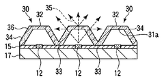
図7および図8に示すように、下側スペーサシート31aは、形状は第1の実施形態と同じであるが、透明シートではなく拡散粒子36を含んだ不透明シートで形成されている。拡散粒子36は、アクリル基材と屈折率の異なる10μm程度の粒子であり、アクリル基材に混ぜ込まれている。実施形態では、拡散粒子36の散乱の平均自由工程を0.002~0.2mm程度に調整し、厚さ0.3mmシートの透過率を50~90%程度とした。これにより、光源12から放射される光線35を下側スペーサシート31aによって周辺に散乱させて、透過反射層25の負担を緩和している。
図7および図9(a)、9(b)に示すように、上側スペーサシート31bは、厚さ0.3mmのアクリル透明シートに、それぞれ同一方向に延びる複数のリブ状の凸部30を付与した形態で、各凸部30の傾斜確度を20~70度程度で均一とし、高さを1~4mm、凸部間の間隔を1~4mm程度としている。このような構成にすることで、上側スペーサシート31bにより若干発生する輝度ムラを均質なものとするとともに、凸部30の畝に垂直な偏光を強く透過させて、前面の液晶表示パネル91の偏光フィルタと一致する光の割合を強めている。
均一な厚さの上側スペーサシート31bではプリズム作用による集光は無く、これによる輝度ムラは生じない。上側スペーサシート31bは、均一の傾斜角を持つ側面領域34を極力増やし、上下平面領域を極力減らす構成としている。そのため、上側スペーサシート31bに入射する角度に依存して反射率が変化することがなく、側面領域と上下平面領域とで凸部30の傾斜による反射率差を無くし、両領域間での輝度ムラを低減することができる。また、凸凹のピッチも4mm程度に細かくして、拡散シート16等により目立たなくさせる配列としている。
上側スペーサシート31bを畝構成としたのは、上述した均一傾斜角の側面を増やす目的のほかに、ブリュースター角付近でスペーサシート31bに入射する光線を増やし、前面の液晶表示パネル91で有効利用される光を増やすためである。下側の導光シート24から放射される光線は様々な方向を向いているが、主体的には導光シート24の垂直方向が最も強くなる。この前方に出た光線35は、スペーサシート31bにより畝に並行な偏光は反射しやすく、垂直な偏光が透過しやすくなる。反射した並行な偏光は、再度背面に戻って反射され、垂直な偏光成分を含んで戻ってくる。この効果は、導光シート24から放射される光線が様々な向きを持つこと、拡散シート16によって偏光が若干乱されることにより偏光選択反射シート19ほどの効果はないが、大きな損失を招くことなくバックライトユニットから放射される光線に偏光を与えることができる。これにより、偏光選択反射シートで反射される光線の割合を軽減し、より光利用効率を改善した液晶表示装置を実現できる。
その他、第2の実施形態に係る面状照明装置および液晶表示装置においても、前述した第1の実施形態と同様の作用効果を得ることができる。
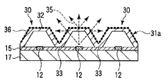
第2の実施形態において、下側スペーサシート31aは、図10に示す第3変形例のように、透明シートの表面に拡散粒子36をコーティングして構成してもよい。また、透明シート表面に微細な凸凹加工を施して、屈折角の分散をしてもよい。いずれの場合も、スペーサシート31aにより光を散乱して透過反射層25の負担を軽減することができる。また、散乱粒子のコーティングや表面加工は、スペーサシートの片面でもよいし、両面に施してもよい。
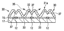
図11および図12に示す第4および第5変形例のように、下側スペーサシート31aにおいて、光源12と対向する各凸部30の接触領域32に小さな凹部37を設け、光源12の直上に配置するようにしてもよい。凹部37は、その形状自体で下側スペーサシート31aへの光の入射角を大きくすることができ、反射成分を増大させて光源12の真上に放射される強い光線を分散する効果がある。図12に示すように、下側スペーサシート31aに拡散粒子36を混ぜた場合、凹部37により、光源12の真上に向かう光線が下側スペーサシート31aを通過する行路長が長くなる分だけ強く散乱され、その結果、透過反射層25の負担を軽減することができる。
次に、第3の実施形態に係る液晶表示装置について説明する。図13は、第3の実施形態に係る面状照明装置を備えた液晶表示装置の断面図である。第3の実施形態において、スペーサシートの構成を除いて、液晶表示装置の他の構成は前述した第1の実施形態と同一であり、異なる部分を詳細に説明し、同一の部分は、第1の実施形態と同一の参照符号を付してその詳細な説明を省略する。
第3の実施形態では、透過反射層25が形成された導光シート24は、スペーサシート31の機能を兼ねるように形成されている。スペーサシート31を兼用した導光シート24以外の構成と原理は、第1の実施形態と同じである。
導光シート24は、それぞれ反射シート15側に突出した複数の凸部30aと、それぞれ拡散シート16側に突出した複数の凸部30bを有している。これらの凸部30a、30bは、透過反射層25の開口率が高く開口率変化がなだらかとなる、隣接する光源12間の部分と対向するように設けられている。各凸部30aの底面は、下側の接触領域33を形成し、反射シート15に接触している。上側の凸部30bの上面は接触領域32を形成し、拡散シート16に接触している。このスペーサシートを兼ねた導光シート24により、拡散シート16が反射シート15と所定の間隔をおいて対向した状態に支持されている。
上記第3の実施形態によれば、導光シートによってシート状の支持部材を構成することにより、積層するシート数を減らすことができ、照明装置を一層軽量化および薄型化することができる。その他、第3の実施形態においても、第1の実施形態と同様の作用効果を得ることができる。
なお、導光シート24のスペーサシート形成部分、すなわち、凸部は、導光シート24の上下両面に設けられているが、これに限らず、導光シートの片面側だけに設ける構成としてもよい。
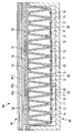
次に、第4の実施形態に係る液晶表示装置について説明する。図14は、第4の実施形態に係る面状照明装置を備えた液晶表示装置の断面図である。本実施形態によれば、スペーサシート31は、凹凸の高さが約50mmの蛇腹構成を有している。スペーサシート31の凹凸配列間隔は、光源12の配列ピッチに対応している。スペーサシート31は、反射シート15上に載置され、このスペーサシート31の上に薄い拡散シート16が支持されている。厚板の拡散板や支柱を廃止している。本実施形態において、透過反射層は用いておらず、支持部材としてのスペーサシート31は拡散シート16を支持する構成としている。
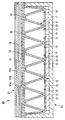
次に、第5の実施形態に係る液晶表示装置について説明する。図15は、第5の実施形態に係る面状照明装置を備えた液晶表示装置の断面図である。本実施形態によれば、スペーサシート31の凸凹配列間隔を光源12の配列ピッチの2倍としている。これにより、スペーサシート31の真空成型時の絞りのアスペクト比が半減し、スペーサシートの成型可能な条件を広くすることができる。
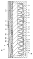
次に、第6の実施形態に係る液晶表示装置について説明する。図16は、第6の実施形態に係る面状照明装置を備えた液晶表示装置の断面図である。本実施形態によれば、反射シート15と拡散シート16との間に、多数の凹凸を有するスペーサシート31cおよび平坦のスペーサシート31dが重ねて配置されている。これにより、スペーサシート31cの凹凸の高さを低くし、真空成型時の絞り量を軽減している。
上述した第4、第5、第6の実施形態において、液晶表示装置の他の構成は、第1の実施形態と同一であり、同一の部分には第1の実施形態と同一の参照符号を付してその詳細な説明を省略する。
次に、第7の実施形態に係る面状照明装置について説明する。図17は、第7の実施形態に係る面状照明装置の断面図である。本実施形態によれば、面状照明装置92は、上面の開口した偏平な箱状のフレーム11と、このフレーム11を土台として設けられた複数の部材とを備えている。すなわち、フレーム11の底面上に、複数の実装基板17が並べて載置され、これらの実装基板17上に、例えば、LEDからなる複数の光源12が実装され、例えば、10~50mm間隔で並べて配置されている。実装基板17上に0.2mm厚さの反射シート15が配置されている。これらの反射シート15は、光源12の部分を除き、互いに連続して並べられている。これにより、複数の光源12は、面状の放射面に設けられている。なお、実装基板17は複数に分割されているが、これに限らず、1枚で構成してもよい。
フレーム11の上部開口を塞ぐように矩形状の拡散板20が配設され、フレーム11の周縁部上に支持されている。拡散板20は、隙間を置いて、光源12および反射シート15とほぼ平行に対向している。拡散板20は、面状の放射面を構成し、ここでは、平坦な矩形状の放射面を構成している。
反射シート15と拡散板20との間に、例えば、厚さ0.2mmのアクリル透明シートからなる矩形状の導光シート24が配置され、反射シート15と隙間を置いて対向している。導光シート24の上面、つまり、拡散板20側の表面、のほぼ全体に亘って、透過反射層25が形成されている。
導光シート24と拡散板20との間に、光透過性および多数の凹凸を有するシート状の支持部材として、例えば、蛇腹状に形成した厚さ0.3mmのアクリル透明シートからなるスペーサシート31が配置されている。スペーサシート31は、導光シート24側に突出する多数の凸部30を有し、各凸部30の上面により形成された接触領域32がそれぞれ導光シート24に固定されている。また、スペーサシート31の拡散板30側の接触領域33は、それぞれ拡散板30に固定されている。スペーサシート31の周縁部は、フレーム11に支持されている。これにより、導光シート24は、スペーサシート31により、拡散板と所定の隙間を置いて対向する状態に支持されている。
照明装置92では、500mm以下の大きさが主流でバックライトユニットほど大型化が必要とされておらず、むしろ薄型化の要求が強い。本実施形態では、薄型化のための透過反射層25を形成した導光シート24を設け、これを支持する部材としてスペーサシート31を用いている。スペーサシート31と導光シート24と拡散板20は、相互に透明接着材で接着固定され、導光シート24はスペーサシート31により所定間隔を保って支持されている。
上記の構成によれば、拡散板20にスペーサシート31と透過反射層25を形成した導光シート24を貼り合わせるだけで、均一輝度で薄型の照明装置を実現することができる。また、導光シートを支持するための多数の支柱を設ける必要がなく、構造の簡素化および装置の一層の薄型化を図ることができる。
次に、他の実施形態に係る面状照明装置について説明する。以下に示す第8、第9、第10、第11の実施形態において、前述した第7の実施形態と異なる部分について詳細に説明し、第7の実施形態と同一の部分には同一の参照符号を付してその詳細な説明を省略する。
図18は、第8の実施形態に係る面状照明装置の断面図である。本実施形態によれば、導光シート24によりスペーサシート31を形成し、導光シートに支持機能を持たせている。すなわち、導光シート24は、拡散板20側に突出した多数の凸部30を有し、各凸部の上面により形成された接触領域32が拡散板20に固定されている。
このような構成によれば、光学シート数を減らすことができ、照明装置の構成の簡素化および一層の薄型化を図ることができる。
このような構成によれば、光学シート数を減らすことができ、照明装置の構成の簡素化および一層の薄型化を図ることができる。
図19は、第9の実施形態に係る面状照明装置の断面図である。本実施形態によれば、スペーサシート31は、導光シート24と反射シート15との間に配置され、導光シート24と反射シート15とに接着固定されている。導光シート24はスペーサシート31により、光源12と所定間隔を保って支持されている。
このような構成においても、第7の実施形態と同様の作用効果を得ることができる。
このような構成においても、第7の実施形態と同様の作用効果を得ることができる。
図20は、第10の実施形態に係る面状照明装置の断面図である。本実施形態によれば、スペーサシート31の機能を導光シート24に持たせ、かつ、その表面に透過反射層25を形成した導光シート24を、光源12側、つまり、反射シート15上に支持している。ここでは、LEDチップの集約された疎な光源の照明装置を示しているが、このような構成の照明装置では、本来の拡散板20がある程度の剛性を有している。そのため、スペーサシート31としては拡散部材を支持する機能よりは、薄型化のための透過反射層25の適切な位置決めの方が重要である。このような構成によれば、シート状のスペーサシート31を兼ねた導光シート24を光源12の基材に乗せる構造により、薄型化を実現でき、生産性も高くなる。
図21は、第11の実施形態に係る面状照明装置の断面図である。本実施形態によれば、透過反射層25を兼ねたスペーサシート31に拡散板20を支持する機能も持たせた構成で、スペーサシート31の支持により拡散板を薄型化してもよい。また、光源12側の基材、ここでは、反射シート15、も平坦に限定されることなく、図21に示すように、凸凹に形成された反射シート15上にスペーサシート31を設置する構成としてもよい。
次に、第12の実施形態に係る液晶表示装置について説明する。図22は、第12の実施形態に係る面状照明装置を備えた液晶表示装置の断面図である。本実施形態によれば、面状照明装置92は、反射シート15上に載置され、透過反射層25を兼ねた下側スペーサシート(支持部材)31aと、この下側スペーサシート31a上に載置された上側スペーサシート(支持部材)31bと、を備え、上側スペーサシート31bにより、拡散シート16を支持している。拡散シート16の上に指向性向上シート18および偏光選択反射シート19が順に積層されている。これら拡散シート16、指向性向上シート18および偏光選択反射シート19により、面状の放射面を構成している。上側スペーサシート31bは、図7に示した第2の実施形態における上側スペーサシートと同じである。
液晶表示装置90では、表示画像にあわせて個々の光源12を複数のグループに分けて点灯輝度を調整できるように構成されている。下側スペーサシート31aは、それぞれ反射シート15a側に突出する複数の領域を有し、これらの領域は、一括して調整する光源12のグループにあわせて、そのグループを区切る側壁31dを構成している。透過反射層25は、通常の各光源12と対向して位置し光輝度均一化を図る領域25aと、点灯輝度を調整する光源12のグループ間を遮蔽する領域25bとを有している。領域25bは、側壁31dの表面に形成され、隣接する点灯輝度領域から漏れ出す光を抑制制御するように機能している。これにより、光源12をグループ毎に分割して点灯輝度を調整する液晶表示装置において、所望の領域毎の輝度プロファイルを形成することができる。
第12の実施形態において、液晶表示装置の他の構成は、前述した第2の実施形態と同一であり、同一の部分には同一の参照符号を付してその詳細な説明を省略する。
次に、第13の実施形態に係る面状照明装置について説明する。図23(a)は、第13の実施形態に係る面状照明装置の平面図、図23(b)は図23(a)の線E-Eに沿った断面図である。本実施形態は、2色からなる掲示版を構成する照明装置である。この照明装置は、従来のような色選択吸収フィルタにより図柄を表示するのではなく、支持部材としてのスペーサシート31に形成した透過反射層25a、25bにより2色の図柄16a、16bを表示するもので、面状の放射面を形成する表層の拡散板16はなんら色選択吸収フィルタを用いていない。すなわち、スペーサシート31は、複数の凹凸を有し、反射シート15上に載置されているとともに、光源12a、12bと対向して設けられた拡散板16を支持している。スペーサシート31の凹凸は、図柄16a、16bにあわせてその色境界に沿って形成された区切り部分31cを有し、この区切り部分31cに遮蔽性の高い透過反射層25bが形成され、スペーサシート31bの他の部分には、光輝度均一化を図る透過反射層25aが形成されている。ここでは、透過反射層25a、25bは、スペーサシート31の拡散板16側も表面上に形成されている。
図柄にあわせて、放出する波長の異なる例えば2種類の光源12a、12bを設け、一方の光源12bを透過反射層25bで囲まれる領域と対向する領域に配置し、他方の光源12aを配置し、透過反射層26bの外側の領域と対向する領域に配置している。透過反射層25bにより、これらの領域間の光の漏れ出しを抑制し、所望の図柄16a、16bを表示する。これにより、より簡単で省電力の掲示版照明装置を提供することが出来る。
第12の実施形態において、照明装置の他の構成は、前述した第2の実施形態と同一であり、同一の部分には同一の参照符号を付してその詳細な説明を省略する。
この発明は上述した実施形態そのままに限定されるものではなく、実施段階ではその要旨を逸脱しない範囲で構成要素を変形して具体化可能である。また、上記実施形態に開示されている複数の構成要素の適宜な組み合わせにより、種々の発明を形成できる。例えば、実施形態に示される全構成要素から幾つかの構成要素を削除してもよい。さらに、異なる実施形態にわたる構成要素を適宜組み合わせてもよい。
例えば、点光源としてのLEDは、白色のものでも、単色のものでも適用可能であり、LEDの種類に関して限定を受けるものではない。
例えば、点光源としてのLEDは、白色のものでも、単色のものでも適用可能であり、LEDの種類に関して限定を受けるものではない。
11…フレーム、12…光源、15…反射シート、16…拡散シート、
24…導光シート、25…透過反射層、30…凸部、31…スペーサシート、
31a…下側スペーサシート、31b…上側スペーサシート、91…液晶表示パネル、
92…面状照明装置
24…導光シート、25…透過反射層、30…凸部、31…スペーサシート、
31a…下側スペーサシート、31b…上側スペーサシート、91…液晶表示パネル、
92…面状照明装置
Claims (20)
- 面状の放射面を有する照明装置であって、
面状の放射面に対向して配置された複数の光源と、
拡散、屈折、反射の少なくとも1つの光学特性を有し、前記光源に対向する光学部材と、
凹凸を有し、前記光学部材を支持する光透過性を有したシート状の支持部材と、
を備える照明装置。 - 前記シート状の支持部材は、全面に亘って均一な厚さを有し、前記光学部材の全面と対向して配置されている請求項1に記載の照明装置。
- 前記光源を支持した光源基材を備え、前記シート状の支持部材は、前記光源基材上に積層されている請求項1記載の照明装置。
- 前記シート状の支持部材は、前記光学部材と一体に形成されている請求項1に記載の照明装置。
- 面状の放射面を形成する拡散板を備え、前記シート状の支持部材は、前記拡散板に積層されている請求項1記載の照明装置。
- それぞれ凹凸を有し、前記光学部材を支持する光透過性を有した2つのシート状の支持部材を備え、これらの支持部材は互いに積層して配置されている請求項1に記載の照明装置。
- 前記支持部材は、積層隣接する部材に接触するための上側および下側の接触領域と、この上側および下側の接触領域を連結し前記複数の光源の中間に対向する側面領域と、を有している請求項1記載の照明装置。
- 前記支持部材の側面領域は、その法線が前記近接する光源に近寄る方向に傾斜している特徴とする請求項7記載の照明装置。
- 前記支持部材の凸凹は、前記複数の光源の配列と同じかその倍数で繰り返し形成されている請求項7記載の照明装置。
- 前記支持部材の凸凹は、前記複数の光源の配列より細かい間隔で繰り返し形成されている請求項7記載の照明装置。
- 前記支持部材は、全ての断面に前記側面領域を含んでいる請求項7記載の照明装置。
- 前記支持部材は、所定の直線あるいは閉曲線で形成される断面において、その他の断面よりも極端に曲げモーメントが小さく形成され、この所定の直線あるいは閉曲面で前記支持部材が曲げられている請求項7記載の照明装置。
- 前記支持部材は、前記複数の光源に対向するそれぞれの領域に形成された凸部を有している請求項7記載の照明装置。
- 前記支持部材の凸凹は、同一方向に平行に延びている請求項7記載の照明装置。
- 前記側面領域の傾斜角度が20~70度である請求項14記載の照明装置。
- 液晶表示パネルと、
前記液晶表示パネルの裏面に設けられた偏光フィルタと、
前記液晶表示パネルに対向して配置され、前記液晶表示パネルに光を照射する請求項14に記載の面状照明装置と、を備え、前記支持部材の凸凹により強まる偏光が前記偏光フィルタを通過する向きである請求項14記載の液晶表示装置。 - 前記支持部材は光散乱性を有している請求項1記載の照明装置。
- 前記支持部材は、凸凹面で外装される体積に対して、実質的な体積が50%以下である請求項1記載の照明装置。
- 前記面状の放射面が曲面である請求項1記載の照明装置。
- 液晶表示パネルと、
前記液晶表示パネルに対向して配置され、前記液晶表示パネルに光を照射する請求項1ないし15、17ないし19のいずれか1項に記載の照明装置と、
を備える液晶表示装置。
Applications Claiming Priority (2)
| Application Number | Priority Date | Filing Date | Title |
|---|---|---|---|
| JP2010-047019 | 2010-03-03 | ||
| JP2010047019A JP5127851B2 (ja) | 2010-03-03 | 2010-03-03 | 面状照明装置およびこれを備えた液晶表示装置 |
Publications (1)
| Publication Number | Publication Date |
|---|---|
| WO2011108603A1 true WO2011108603A1 (ja) | 2011-09-09 |
Family
ID=44542250
Family Applications (1)
| Application Number | Title | Priority Date | Filing Date |
|---|---|---|---|
| PCT/JP2011/054789 Ceased WO2011108603A1 (ja) | 2010-03-03 | 2011-03-02 | 面状照明装置およびこれを備えた液晶表示装置 |
Country Status (2)
| Country | Link |
|---|---|
| JP (1) | JP5127851B2 (ja) |
| WO (1) | WO2011108603A1 (ja) |
Cited By (4)
| Publication number | Priority date | Publication date | Assignee | Title |
|---|---|---|---|---|
| CN107238971A (zh) * | 2017-06-16 | 2017-10-10 | 厦门天马微电子有限公司 | 组合导光板、背光组件和显示面板 |
| CN108604026A (zh) * | 2015-12-31 | 2018-09-28 | 纳米系统公司 | 用于显示器件的背光单元 |
| CN112241087A (zh) * | 2019-07-19 | 2021-01-19 | 船井电机株式会社 | 照明装置和显示装置 |
| EP3767384A1 (en) * | 2019-07-19 | 2021-01-20 | Funai Electric Co., Ltd. | Lighting device and display device |
Families Citing this family (7)
| Publication number | Priority date | Publication date | Assignee | Title |
|---|---|---|---|---|
| TWI589962B (zh) * | 2011-11-04 | 2017-07-01 | 奇菱光電股份有限公司 | 直下式背光模組 |
| JP6065418B2 (ja) * | 2012-06-12 | 2017-01-25 | 凸版印刷株式会社 | 有機el発光体 |
| WO2016175111A1 (ja) * | 2015-04-28 | 2016-11-03 | シャープ株式会社 | 直下型バックライト装置及び液晶表示装置 |
| JP2019075193A (ja) * | 2016-03-10 | 2019-05-16 | パナソニックIpマネジメント株式会社 | バックライト装置及び液晶表示装置 |
| US20200133074A1 (en) * | 2017-04-27 | 2020-04-30 | Sharp Kabushiki Kaisha | Lighting device and display device |
| KR102236084B1 (ko) | 2017-05-03 | 2021-04-02 | 애플 인크. | 지지 포스트들을 갖는 백라이트 유닛들을 갖는 디스플레이들 및 공동 높이 모니터링 |
| JP2019153436A (ja) | 2018-03-01 | 2019-09-12 | シャープ株式会社 | 照明装置および表示装置 |
Citations (2)
| Publication number | Priority date | Publication date | Assignee | Title |
|---|---|---|---|---|
| WO2007148508A1 (ja) * | 2006-06-21 | 2007-12-27 | Idemitsu Kosan Co., Ltd. | 光線反射用多層シート、これを用いた反射器、照明装置及び液晶表示装置 |
| JP2008226636A (ja) * | 2007-03-13 | 2008-09-25 | Sharp Corp | バックライトユニットおよび液晶表示装置 |
-
2010
- 2010-03-03 JP JP2010047019A patent/JP5127851B2/ja not_active Expired - Fee Related
-
2011
- 2011-03-02 WO PCT/JP2011/054789 patent/WO2011108603A1/ja not_active Ceased
Patent Citations (2)
| Publication number | Priority date | Publication date | Assignee | Title |
|---|---|---|---|---|
| WO2007148508A1 (ja) * | 2006-06-21 | 2007-12-27 | Idemitsu Kosan Co., Ltd. | 光線反射用多層シート、これを用いた反射器、照明装置及び液晶表示装置 |
| JP2008226636A (ja) * | 2007-03-13 | 2008-09-25 | Sharp Corp | バックライトユニットおよび液晶表示装置 |
Cited By (8)
| Publication number | Priority date | Publication date | Assignee | Title |
|---|---|---|---|---|
| CN108604026A (zh) * | 2015-12-31 | 2018-09-28 | 纳米系统公司 | 用于显示器件的背光单元 |
| JP2019503558A (ja) * | 2015-12-31 | 2019-02-07 | ナノシス・インク. | 表示装置用のバックライトユニット |
| CN107238971A (zh) * | 2017-06-16 | 2017-10-10 | 厦门天马微电子有限公司 | 组合导光板、背光组件和显示面板 |
| CN112241087A (zh) * | 2019-07-19 | 2021-01-19 | 船井电机株式会社 | 照明装置和显示装置 |
| EP3767383A1 (en) * | 2019-07-19 | 2021-01-20 | Funai Electric Co., Ltd. | Lighting device and display device |
| EP3767384A1 (en) * | 2019-07-19 | 2021-01-20 | Funai Electric Co., Ltd. | Lighting device and display device |
| US10996513B2 (en) | 2019-07-19 | 2021-05-04 | Funai Electric Co., Ltd. | Lighting device and display device |
| CN112241087B (zh) * | 2019-07-19 | 2023-08-11 | 船井电机株式会社 | 照明装置和显示装置 |
Also Published As
| Publication number | Publication date |
|---|---|
| JP2011181464A (ja) | 2011-09-15 |
| JP5127851B2 (ja) | 2013-01-23 |
Similar Documents
| Publication | Publication Date | Title |
|---|---|---|
| JP5127851B2 (ja) | 面状照明装置およびこれを備えた液晶表示装置 | |
| JP5154695B2 (ja) | 照明装置、表示装置、及びテレビ受信装置 | |
| US9341766B2 (en) | Lighting device, display device and television device | |
| US20120013811A1 (en) | Lighting device, display device and television receiver | |
| US8506148B2 (en) | Lighting device, display device and television receiver | |
| JP4461197B1 (ja) | 面状照明装置およびこれを備えた液晶表示装置 | |
| US20220113591A1 (en) | Diffusion plate and backlight module | |
| US8797475B2 (en) | Lighting device, display device and television receiver | |
| US20120236213A1 (en) | Lighting device, display device and television receiver | |
| WO2011074334A1 (ja) | 照明装置、表示装置、及びテレビ受信装置 | |
| JP5138813B2 (ja) | 照明装置、表示装置、及びテレビ受信装置 | |
| KR102266737B1 (ko) | 렌즈, 렌즈를 포함하는 발광 장치, 및 발광 장치를 포함하는 백 라이트 유닛 | |
| US20130050587A1 (en) | Lighting device, display device and television receiver | |
| CN110632698A (zh) | 照明装置和显示装置 | |
| WO2019021952A1 (ja) | 照明装置及び表示装置 | |
| JP2010108601A (ja) | 面状光源及び液晶表示装置 | |
| US8405796B2 (en) | Illumination device, surface light source device, and liquid crystal display device | |
| JP2010102905A (ja) | 面状光源及び液晶表示装置 | |
| KR20150066847A (ko) | 광속 제어 부재, 발광 장치 및 표시장치 | |
| TWI701486B (zh) | 背光模組及具有背光模組之顯示裝置 | |
| KR20120052627A (ko) | 액정표시장치 | |
| TW202131051A (zh) | 配光控制元件 | |
| KR20070115483A (ko) | 고출력 도광판 및 이를 채용한 백라이트 유닛 | |
| CN205028004U (zh) | 背光模组与显示装置 | |
| WO2011114790A1 (ja) | 照明装置、表示装置及びテレビ受信装置 |
Legal Events
| Date | Code | Title | Description |
|---|---|---|---|
| 121 | Ep: the epo has been informed by wipo that ep was designated in this application |
Ref document number: 11750712 Country of ref document: EP Kind code of ref document: A1 |
|
| NENP | Non-entry into the national phase |
Ref country code: DE |
|
| 122 | Ep: pct application non-entry in european phase |
Ref document number: 11750712 Country of ref document: EP Kind code of ref document: A1 |