WO2011108296A1 - 焦電型赤外線センサー装置 - Google Patents
焦電型赤外線センサー装置 Download PDFInfo
- Publication number
- WO2011108296A1 WO2011108296A1 PCT/JP2011/050521 JP2011050521W WO2011108296A1 WO 2011108296 A1 WO2011108296 A1 WO 2011108296A1 JP 2011050521 W JP2011050521 W JP 2011050521W WO 2011108296 A1 WO2011108296 A1 WO 2011108296A1
- Authority
- WO
- WIPO (PCT)
- Prior art keywords
- infrared sensor
- region
- pyroelectric
- sensor device
- receiving surface
- Prior art date
- Legal status (The legal status is an assumption and is not a legal conclusion. Google has not performed a legal analysis and makes no representation as to the accuracy of the status listed.)
- Ceased
Links
Images




Classifications
-
- G—PHYSICS
- G01—MEASURING; TESTING
- G01J—MEASUREMENT OF INTENSITY, VELOCITY, SPECTRAL CONTENT, POLARISATION, PHASE OR PULSE CHARACTERISTICS OF INFRARED, VISIBLE OR ULTRAVIOLET LIGHT; COLORIMETRY; RADIATION PYROMETRY
- G01J5/00—Radiation pyrometry, e.g. infrared or optical thermometry
- G01J5/10—Radiation pyrometry, e.g. infrared or optical thermometry using electric radiation detectors
- G01J5/34—Radiation pyrometry, e.g. infrared or optical thermometry using electric radiation detectors using capacitors, e.g. pyroelectric capacitors
-
- G—PHYSICS
- G01—MEASURING; TESTING
- G01J—MEASUREMENT OF INTENSITY, VELOCITY, SPECTRAL CONTENT, POLARISATION, PHASE OR PULSE CHARACTERISTICS OF INFRARED, VISIBLE OR ULTRAVIOLET LIGHT; COLORIMETRY; RADIATION PYROMETRY
- G01J5/00—Radiation pyrometry, e.g. infrared or optical thermometry
- G01J5/02—Constructional details
- G01J5/08—Optical arrangements
- G01J5/0831—Masks; Aperture plates; Spatial light modulators
Definitions
- the present invention relates to a pyroelectric infrared sensor device.
- the present invention relates to a pyroelectric substrate having a light receiving surface, a first electrode formed on the light receiving surface of the pyroelectric substrate, and a second formed on the pyroelectric substrate.
- the present invention relates to a pyroelectric infrared sensor device including a pyroelectric infrared sensor having a plurality of electrodes.
- an infrared sensor device using infrared rays is known as a sensor device that detects temperature without contact.
- a pyroelectric infrared sensor device using the pyroelectric effect of the pyroelectric substrate can be cited.
- Pyroelectric infrared sensor device has differential output characteristics. For this reason, the pyroelectric infrared sensor device generates an output only when the amount of incident infrared rays changes. Therefore, the pyroelectric infrared sensor device generates an output when, for example, an object that generates heat such as a person or an animal crosses the detection area. Therefore, the pyroelectric infrared sensor device is widely used as a human detection sensor or the like.
- Patent Document 1 and Patent Document 2 a plurality of pyroelectric infrared sensors are provided in an array, a chopper is provided in front of the sensor array, and the sensor array itself is rotated. It has been proposed.
- Patent Documents 1 and 2 when a large number of pyroelectric infrared sensors are used, the device structure tends to be complicated and the sensor device tends to be enlarged. In addition, it is necessary to provide a chopper or a sensor array drive device, which causes a problem that the structure of the sensor device is further complicated and the sensor device is further increased in size.
- the present invention has been made in view of the above points, and an object thereof is to provide an infrared sensor device capable of detecting in detail the movement of a heat source, having a simple structure, and a small-sized infrared sensor device. It is in.
- the pyroelectric infrared sensor device includes a pyroelectric infrared sensor and an optical filter.
- the pyroelectric infrared sensor has a pyroelectric substrate, a first electrode, and a second electrode.
- the pyroelectric substrate has a light receiving surface.
- the first electrode is formed on the light receiving surface of the pyroelectric substrate.
- the second electrode is formed on the pyroelectric substrate.
- the optical filter is disposed on the light receiving surface of the pyroelectric infrared sensor. The optical filter reduces the intensity of the incident infrared light with respect to a part of the first electrode, whereby the intensity of the incident infrared light is relatively high in the region where the first electrode is provided.
- An area and a second area where the intensity of incident infrared rays is relatively low are formed.
- the pyroelectric infrared sensor device detects the movement of a heat source that moves in the detection direction.
- the optical filter is configured such that the first region is located on both sides of the detection direction of the second region.
- the length in the detection direction of the first region located on one side of the detection direction of the second region, and the detection direction of the second region is equal.
- the output level when infrared rays are incident on the first region is the same, and the presence or absence of a heat source can be determined based on one criterion.
- the detection direction includes a first detection direction and a second detection direction that forms an angle with respect to the first detection direction.
- the movement of the heat source moving in a plurality of detection directions including the first and second detection directions can be detected in detail.
- the optical filter includes a plurality of regions separated by the second region and the second region in the region where the first electrode is provided.
- the first region is formed, and the plurality of first regions are formed in a matrix.
- the optical filter has a relatively high infrared transmittance, a high transmittance portion that forms the first region, and an infrared transmittance. Is relatively low and has a low transmittance part forming the second region.
- the pyroelectric substrate has a back surface facing the light receiving surface, and the second electrode is formed on the back surface.
- a first region where the intensity of incident infrared light is relatively high and a second region where the intensity of incident infrared light is relatively low are formed in the region where the first electrode is provided. ing. For this reason, when infrared rays incident from the heat source move from one of the first and second regions to the other, an output is generated due to the pyroelectric effect of the pyroelectric substrate.
- an output signal is output by the movement of the heat source within the detection area of the pyroelectric infrared sensor. Therefore, the movement of the heat source can be detected in detail with a smaller number of sensors. That is, according to the present invention, it is possible to provide an infrared sensor device that can detect the movement of the heat source in detail and has a simple structure and a small size.
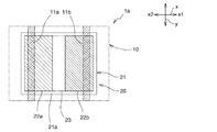
- FIG. 1A is a schematic side view of the pyroelectric infrared sensor device according to the first embodiment.
- FIG. 1B is a time chart showing an output signal from the pyroelectric infrared sensor device according to the first embodiment.
- FIG. 2 is a schematic plan view of the pyroelectric infrared sensor device according to the first embodiment.
- FIG. 3 is a schematic perspective view of the optical filter.
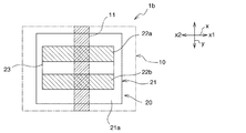
- FIG. 4 is a schematic plan view of a pyroelectric infrared sensor device according to the second embodiment.
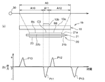
- FIG. 5A is a schematic side view of a pyroelectric infrared sensor device according to the second embodiment.
- FIG. 5B is a time chart showing an output signal from the pyroelectric infrared sensor device according to the second embodiment.
- FIG. 6 is a schematic plan view of a pyroelectric infrared sensor device according to the third embodiment.
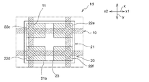
- FIG. 7 is a schematic plan view of a pyroelectric infrared sensor device according to the fourth embodiment.
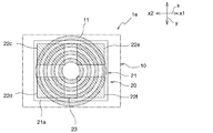
- FIG. 8 is a schematic plan view of a pyroelectric infrared sensor device according to the fifth embodiment.
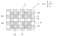
- FIG. 9 is a schematic plan view of a pyroelectric infrared sensor device according to the sixth embodiment.
- FIG. 10 is a schematic cross-sectional view of a pyroelectric infrared sensor device according to the seventh embodiment.
- pyroelectric infrared sensor devices 1a to 1f shown in FIGS. 1, 2, 4 to 9 as examples.
- the pyroelectric infrared sensor devices 1a to 1f are merely examples.
- the pyroelectric infrared sensor device according to the present invention is not limited to the pyroelectric infrared sensor devices 1a to 1f.
- FIG. 1A is a schematic side view of the pyroelectric infrared sensor device according to the first embodiment.
- FIG. 1B is a time chart showing an output signal from the pyroelectric infrared sensor device according to the first embodiment.
- FIG. 2 is a schematic plan view of the pyroelectric infrared sensor device according to the first embodiment.
- FIG. 3 is a schematic perspective view of the optical filter. In FIG. 2, for convenience of explanation, the region where the light receiving surface electrodes 22 a and 22 b are provided and the region where the linear grooves 11 a and 11 b are provided are hatched.
- the pyroelectric infrared sensor device 1a shown in FIGS. 1 and 2 is a sensor device that detects the movement of the heat source 30 that moves in the x direction.
- the pyroelectric infrared sensor device 1 a includes a pyroelectric infrared sensor 20 and an optical filter 10.
- the pyroelectric infrared sensor 20 includes a pyroelectric substrate 21.
- the pyroelectric substrate 21 has a light receiving surface 21a that receives infrared light and a back surface 21b that faces the light receiving surface 21a.
- the pyroelectric substrate 21 is made of a pyroelectric material that generates a voltage when receiving infrared rays. Specific examples of the pyroelectric material include LiTaO 3 .
- each of the light receiving surface electrodes 22a and 22b is formed in a rectangular shape extending in the y direction perpendicular to the x direction.
- the light receiving surface electrodes 22a and 22b are arranged at intervals in the x direction.
- a back surface electrode 23 as a second electrode is formed on the back surface 21b of the pyroelectric substrate 21.
- Each of the light receiving surface electrodes 22a and 22b and the back surface electrode 23 can be formed of an appropriate conductive material such as a metal or an alloy. Specifically, each of the light receiving surface electrodes 22a and 22b and the back surface electrode 23 can be formed of, for example, a Ni alloy or a Cu alloy.
- the optical filter 10 is disposed on the light receiving surface 21 a of the pyroelectric infrared sensor 20.
- the optical filter 10 is made of a material such as silicon that transmits infrared rays.
- the optical filter 10 reduces the intensity of the incident infrared light to a part of the light receiving surface electrodes 22a and 22b, so that the intensity of the incident infrared light is reduced in each of the regions where the light receiving surface electrodes 22a and 22b are provided.
- the first regions B1 to B4 having a relatively high level and the second regions C1 and C2 having a relatively low intensity of incident infrared rays are formed.
- a plurality of linear grooves 11a and 11b extending in the y direction are formed in the optical filter 10 made of a material that transmits infrared rays such as silicon.
- the bottom surfaces 11a1 and 11b1 of these linear grooves 11a and 11b are formed into rough surfaces. For this reason, the transmittance
- the region in which the linear grooves 11a and 11b are formed in the optical filter 10 constitutes a low transmittance portion having a relatively low infrared transmittance.
- the region of the optical filter 10 where the linear grooves 11a and 11b are not formed constitutes a high transmittance part with relatively low infrared transmittance.
- the second region where the relatively low-infrared light that has passed through the first regions B1 to B4 where the relatively high infrared rays are incident and the portions where the linear grooves 11a and 11b of the optical filter 10 are formed is incident. Regions C1 and C2 are formed.
- the optical filter 10 is configured such that the first regions B1, B3 and B2, B4 are located on both sides of the second regions C1, C2 in the x direction. That is, the linear grooves 11a and 11b are formed at positions where the first regions B1, B3 and B2, B4 are located on both sides in the x direction of the second regions C1, C2.
- the part in which the linear grooves 11a and 11b of the optical filter 10 are formed may absorb a part of infrared rays or may substantially block infrared rays.
- the dimensions of the linear grooves 11a and 11b can be appropriately set according to characteristics required for the sensor device.
- the linear grooves 11a and 11b can have, for example, a width of about 0.03 mm to 2.0 mm and a depth of about 0.01 mm to 0.2 mm.
- the formation of the linear grooves 11a and 11b can be performed by, for example, dicing.
- the heat source 30 When the heat source 30 is located in the detection area A1, the amount of infrared rays incident from the heat source 30 does not change.
- the heat source 30 moves from the detection area A1 to the non-detection area A2, at least a part of infrared rays from the heat source 30 is shielded by the linear groove 11a. For this reason, a signal P2 having a polarity opposite to that of the signal P1 is output between the light receiving surface electrode 22a and the back surface electrode 23.
- the heat source 30 moves from the non-detection area A2 to the detection area A3, the amount of infrared rays incident on the portion of the pyroelectric substrate 21 located below the light receiving surface electrode 22a increases. For this reason, the signal P3 having the same polarity as the signal P1 is output.
- the infrared rays from the heat source 30 do not enter the light receiving surface electrode 22a. For this reason, the signal P4 is output.
- the heat source 30 moves from the detection area A5 to the non-detection area A6 and when the heat source 30 moves from the detection area A7 to the outside of the detection area A7, the heat source 30 is located below the light receiving surface electrode 22b of the pyroelectric substrate 21. Since the amount of infrared rays incident on the portion decreases, signals P6 and P8 are output.
- the optical filter 10 causes the first regions B1 to B4 having relatively high intensity of incident infrared rays to the regions where the light receiving surface electrodes 22a and 22b are provided.
- the second regions C1 and C2 having relatively low intensity of incident infrared rays are formed. For this reason, as described above, when the heat source 30 moves from the x2 side in the x direction to the x1 side in each of the light receiving surface electrodes 22a and 22b, a plurality of signals are output.
- a signal P1 indicating that the heat source 30 has moved to the detection area A1 a signal P2 indicating that the heat source 30 has moved from the area A1 to the area A2, and a heat source 30 from the area A2.
- a signal P3 indicating the movement to the area A3 and a signal P4 indicating that the heat source 30 has moved from the area A3 to the area A4 are output.
- a signal P7 indicating movement to A7 and a signal P8 indicating that the heat source 30 has moved from the area A7 to the x1 side are output. Therefore, in the present embodiment, the movement of the heat source 30 can be detected in detail with a small number of sensors and light receiving surface electrodes. That is, the pyroelectric infrared sensor device 1a of the present embodiment has a simple structure and is small in size, and can detect the movement of the heat source 30 in detail.
- FIG. 4 is a schematic plan view of a pyroelectric infrared sensor device 1b according to the second embodiment.
- FIG. 5A is a schematic side view of a pyroelectric infrared sensor device 1b according to the second embodiment.
- FIG. 5B is a time chart showing an output signal from the pyroelectric infrared sensor device 1b according to the second embodiment.
- the region where the light receiving surface electrodes 22 a and 22 b are provided and the region where the low transmittance part 11 is provided are hatched.
- the present invention is not limited to this configuration.
- the light receiving surface electrodes 22 a and 22 b are formed in a rectangular shape extending along the x direction, and are arranged along the y direction.
- the low transmittance part 11 of the optical filter 10 is provided in the center part in the x direction of the light-receiving surface electrodes 22a and 22b.
- the optical filter 10 includes first regions B5 and B6 in which the intensity of incident infrared rays is relatively high in the second region C3 in the x direction. It is provided so that it may be located on both sides.
- the length of the first region B5 in the x direction is equal to the length of the first region B6 in the x direction.
- the low transmittance portion 11 may be formed by providing a shielding member 10b that shields infrared rays on a transmission member 10a that transmits infrared rays.
- the transmitting member 10a that transmits infrared light can be formed of, for example, silicon.
- the shielding member 10b that shields infrared rays can be formed of, for example, a metal film, a coating film, glass that absorbs infrared rays, or the like.
- the pyroelectric infrared sensor device 1b has a simple structure and is small in size, like the pyroelectric infrared sensor device 1a according to the first embodiment, and the movement of the heat source 30 in detail. Can be detected.
- FIG. 6 is a schematic plan view of a pyroelectric infrared sensor device 1c according to the third embodiment.
- hatching is added to the region where the light receiving surface electrodes 22c to 22f are provided and the region where the low transmittance portion 11 is provided.
- the present invention is not limited to this configuration. Only one light receiving surface electrode may be provided, or three or more light receiving surface electrodes may be provided.
- four light receiving surface electrodes 22c to 22f are formed in a matrix.
- the movement of the heat source not only in the x direction but also in the y direction can be detected by separately detecting the signals from the light receiving surface electrodes 22c and 22e and the signals from the light receiving surface electrodes 22d and 22f. .
- FIG. 7 is a schematic plan view of a pyroelectric infrared sensor device 1d according to the fourth embodiment.
- the region where the light receiving surface electrodes 22c to 22f are provided and the region where the low transmittance part 11 is provided are hatched.
- the present invention is not limited to this configuration.
- a plurality of first regions having relatively high intensity of incident infrared rays are formed in a matrix in each of the regions where the light receiving surface electrodes 22c, 22d, 22e, and 22f are provided.
- the low transmittance portion 11 is formed in a lattice shape. According to this configuration, it is possible to detect in detail not only the x direction but also the movement of the heat source 30 in the y direction.
- FIG. 8 is a schematic plan view of a pyroelectric infrared sensor device e according to the fifth embodiment.
- FIG. 9 is a schematic plan view of a pyroelectric infrared sensor device f according to the sixth embodiment.
- the region where the light receiving surface electrodes 22 c to 22 f are provided and the region where the low transmittance part 11 is provided are hatched.
- the low transmittance portion 11 is formed in a linear shape or a lattice shape.
- the present invention is not limited to this configuration.
- the low transmittance portion 11 may be formed in a concentric shape.
- the low transmittance part 11 may be formed in a matrix as shown in FIG. 9, for example. Even in these cases, similarly to the pyroelectric infrared sensor device 1d according to the fourth embodiment, it is possible to detect in detail not only the x direction but also the movement of the heat source 30 in the y direction.
- FIG. 10 is a schematic cross-sectional view of a pyroelectric infrared sensor device according to the seventh embodiment.
- the pyroelectric infrared sensor device according to the present embodiment is provided with a light shielding member 40 between the light receiving surface electrodes 22a and 22b in plan view.
- the light shielding member 40 is attached to the optical filter 10.
- infrared rays from the detection areas A1 to A3 may enter the light receiving surface electrode 22a and may also enter the light receiving surface electrode 22b.
- the infrared rays from the detection areas A5 to A7 may enter the light receiving surface electrode 22b and may also enter the light receiving surface electrode 22a.
- the output on the light receiving surface electrode 22a side and the output on the light receiving surface electrode 22b side cancel each other, and the sensing ability decreases. There is a risk of it.
- the light shielding member 40 is provided so that infrared light from one heat source is incident exclusively on one of the plurality of light receiving surface electrodes and not on the other light receiving surface electrodes. For this reason, high sensing ability can be realized.
Landscapes
- Physics & Mathematics (AREA)
- General Physics & Mathematics (AREA)
- Spectroscopy & Molecular Physics (AREA)
- Engineering & Computer Science (AREA)
- Power Engineering (AREA)
- Photometry And Measurement Of Optical Pulse Characteristics (AREA)
- Indicating Or Recording The Presence, Absence, Or Direction Of Movement (AREA)
Abstract
熱源の移動を詳細に検知可能である赤外線センサー装置であって、構造がシンプルで、小型な赤外線センサー装置を提供する。 焦電型赤外線センサー装置1aは、焦電型赤外線センサー20と、光学フィルタ10とを備えている。焦電型赤外線センサー20は、受光面21aを有する焦電体基板21と、受光面21aの上に形成されている第1の電極22a、22bと、焦電体基板21の上に形成されている第2の電極23とを有する。光学フィルタ10は、受光面21aの上に配置されている。光学フィルタ10は、第1の電極22a、22bの一部に対して入射する赤外線の強度を低下させることにより、第1の電極22a、22bが設けられている領域に、入射する赤外線の強度が相対的に高い第1の領域B1~B4と、入射する赤外線の強度が相対的に低い第2の領域C1,C2とを形成している。
Description
本発明は、焦電型赤外線センサー装置に関する。特には、本発明は、受光面を有する焦電体基板と、焦電体基板の受光面の上に形成されている第1の電極と、焦電体基板の上に形成されている第2の電極とを有する焦電型赤外線センサーを備える焦電型赤外線センサー装置に関する。
従来、例えば、非接触で温度を検出するセンサー装置として、赤外線を利用する赤外線センサー装置が知られている。この赤外線センサー装置の具体例としては、例えば、焦電体基板の焦電効果を利用した焦電型の赤外線センサー装置が挙げられる。
焦電型赤外線センサー装置は、微分出力特性有している。このため、焦電型赤外線センサー装置は、入射する赤外線量が変化したときのみ出力を発生させる。よって、焦電型赤外線センサー装置は、例えば、人や動物などの熱を発する物体が検知エリアを横切ったときに出力を発生させる。従って、焦電型赤外線センサー装置は、人検知センサーなどとして、広く利用されている。
しかしながら、従来の焦電型赤外線センサー装置では、人の二次元的な挙動を詳細にセンシングしたり、空間の温度分布を正確にセンシングしたりすることは困難であった。
このことに鑑み、例えば、下記の特許文献1や、特許文献2においては、複数の焦電型赤外線センサーをアレイ状に設け、そのセンサアレイの前にチョッパーを設けると共に、センサアレイ自身を回転させることが提案されている。
しかしながら、上記特許文献1,2に記載のように、多数の焦電型赤外線センサーを用いると、素子構造が複雑になると共に、センサー装置が大型化する傾向にあった。また、チョッパーやセンサアレイの駆動装置を設ける必要があり、センサー装置の構造がさらに複雑になると共に、センサー装置がさらに大型化するという問題があった。
本発明は、かかる点に鑑みてなされたものであり、その目的は、熱源の移動を詳細に検知可能である赤外線センサー装置であって、構造がシンプルで、小型な赤外線センサー装置を提供することにある。
本発明に係る焦電型赤外線センサー装置は、焦電型赤外線センサーと、光学フィルタとを備えている。焦電型赤外線センサーは、焦電体基板と、第1の電極と、第2の電極とを有する。焦電体基板は、受光面を有する。第1の電極は、焦電体基板の受光面の上に形成されている。第2の電極は、焦電体基板の上に形成されている。光学フィルタは、焦電型赤外線センサーの受光面の上に配置されている。光学フィルタは、第1の電極の一部に対して入射する赤外線の強度を低下させることにより、第1の電極が設けられている領域に、入射する赤外線の強度が相対的に高い第1の領域と、入射する赤外線の強度が相対的に低い第2の領域とを形成している。
本発明に係る焦電型赤外線センサー装置のある特定の局面では、焦電型赤外線センサー装置は、検知方向に移動する熱源の移動を検知するものである。光学フィルタは、第2の領域の検知方向の両側に、第1の領域が位置するように構成されている。
本発明に係る焦電型赤外線センサー装置の他の特定の局面では、第2の領域の検知方向の一方側に位置する第1の領域の検知方向における長さと、第2の領域の検知方向の他方側に位置する第1の領域の検知方向における長さとが等しい。この構成では、第1の領域に赤外線が入射したときの出力レベルが同じとなり、熱源の有無を一つの基準で判断できる。
本発明に係る焦電型赤外線センサー装置の別の特定の局面では、検知方向には、第1の検知方向と、第1の検知方向に対して角度を成す第2の検知方向とが含まれる。この構成では、第1及び第2の検出方向を含む複数の検出方向に移動する熱源の移動を詳細に検知することができる。
本発明に係る焦電型赤外線センサー装置のさらに他の特定の局面では、光学フィルタは、第1の電極が設けられている領域に、第2の領域と、第2の領域により隔離された複数の第1の領域を形成し、複数の第1の領域は、マトリクス状に形成されている。この構成では、複数の検出方向に移動する熱源の移動を詳細に検知することができる。
本発明に係る焦電型赤外線センサー装置のさらに別の特定の局面では、光学フィルタは、赤外線の透過率が相対的に高く、第1の領域を形成する高透過率部と、赤外線の透過率が相対的に低く、第2の領域を形成する低透過率部とを有する。
本発明に係る焦電型赤外線センサー装置のまた他の特定の局面では、焦電体基板は、受光面に対向している裏面を有し、第2の電極は、裏面上に形成されている。
本発明では、第1の電極が設けられている領域に、入射する赤外線の強度が相対的に高い第1の領域と、入射する赤外線の強度が相対的に低い第2の領域とが形成されている。このため、熱源から入射する赤外線が、第1及び第2の領域の一方から他方に移動したときなどに、焦電体基板の焦電効果により、出力が発生する。このように、本発明では、焦電型赤外線センサーがひとつのみ設けられている場合であっても、焦電型赤外線センサーの検知エリア内における熱源の移動によって出力信号が出力される。従って、より少ないセンサー数で、熱源の移動を詳細に検知することができる。すなわち、本発明によれば、熱源の移動を詳細に検知可能である赤外線センサー装置であって、構造がシンプルで、小型な赤外線センサー装置を提供することができる。
以下、本発明を実施した好ましい形態について、図1,2,4~9に示す焦電型赤外線センサー装置1a~1fを例に挙げて説明する。但し、焦電型赤外線センサー装置1a~1fは単なる例示である。本発明に係る焦電型赤外線センサー装置は、焦電型赤外線センサー装置1a~1fに何ら限定されない。
《第1の実施形態》
図1(a)は、第1の実施形態に係る焦電型赤外線センサー装置の模式的側面図である。図1(b)は、第1の実施形態に係る焦電型赤外線センサー装置からの出力信号を表すタイムチャートである。図2は、第1の実施形態に係る焦電型赤外線センサー装置の模式的平面図である。図3は、光学フィルタの模式的斜視図である。なお、図2においては、説明の便宜上、受光面電極22a、22bが設けられている領域及び線条溝11a、11bが設けられている領域にハッチングを附している。
図1(a)は、第1の実施形態に係る焦電型赤外線センサー装置の模式的側面図である。図1(b)は、第1の実施形態に係る焦電型赤外線センサー装置からの出力信号を表すタイムチャートである。図2は、第1の実施形態に係る焦電型赤外線センサー装置の模式的平面図である。図3は、光学フィルタの模式的斜視図である。なお、図2においては、説明の便宜上、受光面電極22a、22bが設けられている領域及び線条溝11a、11bが設けられている領域にハッチングを附している。
(焦電型赤外線センサー装置1aの構成)
図1及び図2に示す焦電型赤外線センサー装置1aは、x方向に移動する熱源30の移動を検知するセンサー装置である。
図1及び図2に示す焦電型赤外線センサー装置1aは、x方向に移動する熱源30の移動を検知するセンサー装置である。
図1及び図2に示すように、焦電型赤外線センサー装置1aは、焦電型赤外線センサー20と、光学フィルタ10とを備えている。
焦電型赤外線センサー20は、焦電体基板21を備えている。焦電体基板21は、赤外線を受光する受光面21aと、受光面21aに対向している裏面21bとを有する。焦電体基板21は、赤外線を受光した際に電圧を発生させる焦電体からなるものである。焦電体の具体例としては、LiTaO3などが挙げられる。
焦電体基板21の受光面21aの上には、第1の電極としての受光面電極22a、22bが形成されている。図2に示すように、受光面電極22a、22bのそれぞれは、x方向に対して垂直なy方向に延びる矩形状に形成されている。受光面電極22a、22bは、x方向に相互に間隔をおいて配列されている。
一方、焦電体基板21の裏面21bの上には、第2の電極としての裏面電極23が形成されている。
なお、受光面電極22a、22b及び裏面電極23のそれぞれは、金属や合金などの、適宜の導電材料により形成することができる。具体的には、受光面電極22a、22b及び裏面電極23のそれぞれは、例えば、Ni合金やCu合金などにより形成することができる。
図1に示すように、光学フィルタ10は、焦電型赤外線センサー20の受光面21aの上に配置されている。本実施形態において、光学フィルタ10は、赤外線を透過させるシリコンなどの材料からなる。
光学フィルタ10は、受光面電極22a、22bの一部に対して入射する赤外線の強度を低下させることにより、受光面電極22a、22bが設けられている領域のそれぞれに、入射する赤外線の強度が相対的に高い第1の領域B1~B4と、入射する赤外線の強度が相対的に低い第2の領域C1,C2とを形成している。
具体的には、図3に示すように、シリコンなどの赤外線を透過させる材料からなる光学フィルタ10には、y方向に延びる複数の線条溝11a、11bが形成されている。これら線条溝11a、11bの底面11a1,11b1は、粗面に形成されている。このため、光学フィルタ10のうち、線条溝11a、11bが形成されている部分における赤外線の透過率は、線条溝11a、11bが形成されていない部分における赤外線の透過率よりも低い。従って、光学フィルタ10のうち、線条溝11a、11bが形成されている領域は、赤外線の透過率が相対的に低い低透過率部を構成している。一方、光学フィルタ10のうち、線条溝11a、11bが形成されていない領域は、赤外線の透過率が相対的に低い高透過率部を構成している。
よって、図1(a)に示すように、受光面電極22a、22bが設けられている領域のそれぞれに、光学フィルタ10の線条溝11a、11bが形成されていない部分を透過した、強度が相対的に高い赤外線が入射する第1の領域B1~B4と、光学フィルタ10の線条溝11a、11bが形成されている部分を透過した、強度が相対的に低い赤外線が入射する第2の領域C1,C2とが形成される。
詳細には、本実施形態においては、光学フィルタ10は、第2の領域C1,C2のx方向の両側に、第1の領域B1,B3及びB2,B4が位置するように構成されている。すなわち、線条溝11a、11bは、第2の領域C1,C2のx方向の両側に、第1の領域B1,B3及びB2,B4が位置するような位置に形成されている。
なお、光学フィルタ10の線条溝11a、11bが形成されている部分は、赤外線の一部を吸収するものであってもよいし、赤外線を実質的に遮蔽するものであってもよい。
線条溝11a、11bの寸法は、センサー装置に要求される特性などに応じて適宜設定することができる。線条溝11a、11bは、例えば、幅:0.03mm~2.0mm程度、深さ:0.01mm~0.2mm程度とすることができる。線条溝11a、11bの形成は、例えば、ダイシングなどにより行うことができる。
(焦電型赤外線センサー装置1aの動作原理)
次に、図1を主として参照しながら、焦電型赤外線センサー装置1aの動作原理について説明する。なお、ここでは、図1に示す熱源30が、検知方向であるx方向のx2側からx1側に移動したときを例に挙げて説明する。
次に、図1を主として参照しながら、焦電型赤外線センサー装置1aの動作原理について説明する。なお、ここでは、図1に示す熱源30が、検知方向であるx方向のx2側からx1側に移動したときを例に挙げて説明する。
熱源30がエリアA0よりもx2側から第1の検知エリアA1に移動すると、受光面電極22a上に赤外線が入射する。このため、焦電体基板21の受光面電極22aの下に位置する部分が加熱され、電荷が発生する。これにより、図1(b)に示すように、受光面電極22aと裏面電極23との間に電位差が発生し、その結果、信号P1が出力される。
熱源30が検知エリアA1内に位置しているときは、熱源30から入射する赤外線量は変化しない。熱源30が検知エリアA1から非検知エリアA2に移動すると、熱源30からの赤外線の少なくとも一部が線条溝11aによって遮蔽される。このため、受光面電極22aと裏面電極23との間に、信号P1とは逆極性の信号P2が出力される。
熱源30が非検知エリアA2から検知エリアA3に移動すると、熱源30から焦電体基板21の受光面電極22aの下に位置する部分に入射する赤外線量が増大する。このため、信号P1と同極性の信号P3が出力される。
熱源30が検知エリアA3から、非検知エリアA4に移動すると、熱源30からの赤外線が受光面電極22aに入射しなくなる。このため、信号P4が出力される。
熱源30が非検知エリアA4から検知エリアA5へ移動したとき、及び非検知エリアA6から検知エリアA7へ移動したときには、焦電体基板21の受光面電極22bの下に位置する部分に入射する赤外線量が増大するため信号P5,P7が出力される。
一方、熱源30が検知エリアA5から非検知エリアA6に移動したとき、及び熱源30が検知エリアA7から検知エリアA7外に移動したときには、焦電体基板21の受光面電極22bの下に位置する部分に入射する赤外線量が減少するため、信号P6,P8が出力される。
以上説明したように、本実施形態では、光学フィルタ10により、受光面電極22a、22bが設けられている領域のそれぞれに、入射する赤外線の強度が相対的に高い第1の領域B1~B4と、入射する赤外線の強度が相対的に低い第2の領域C1,C2とが形成されている。このため、上述のように、受光面電極22a、22bのそれぞれにおいて、熱源30がx方向のx2側からx1側に移動したときに、複数の信号が出力される。具体的には、受光面電極22aからは、熱源30が検知エリアA1に移動したことを示す信号P1、熱源30がエリアA1からエリアA2に移動したことを示す信号P2、熱源30がエリアA2からエリアA3に移動したことを示す信号P3、及び熱源30がエリアA3からエリアA4に移動したことを示す信号P4が出力される。また、受光面電極22bからは、熱源30がエリアA4からエリアA5に移動したことを示す信号P5、熱源30がエリアA5からエリアA6に移動したことを示す信号P6、熱源30がエリアA6からエリアA7に移動したことを示す信号P7,及び熱源30がエリアA7からx1側に移動したことを示す信号P8が出力される。従って、本実施形態では、少ないセンサー数及び受光面電極数で、熱源30の移動を詳細に検知することができる。すなわち、本実施形態の焦電型赤外線センサー装置1aは、シンプルな構造で、小型でありつつ、熱源30の移動を詳細に検知することができる。
以下、本発明を実施した好ましい形態の他の例について説明する。なお、以下の説明において、上記第1の実施形態と実質的に共通の機能を有する部材を共通の機能で参照し、説明を省略する。
《第2の実施形態》
図4は、第2の実施形態に係る焦電型赤外線センサー装置1bの模式的平面図である。図5(a)は、第2の実施形態に係る焦電型赤外線センサー装置1bの模式的側面図である。図5(b)は、第2の実施形態に係る焦電型赤外線センサー装置1bからの出力信号を表すタイムチャートである。なお、図4においては、説明の便宜上、受光面電極22a、22bが設けられている領域及び低透過率部11が設けられている領域にハッチングを附している。
図4は、第2の実施形態に係る焦電型赤外線センサー装置1bの模式的平面図である。図5(a)は、第2の実施形態に係る焦電型赤外線センサー装置1bの模式的側面図である。図5(b)は、第2の実施形態に係る焦電型赤外線センサー装置1bからの出力信号を表すタイムチャートである。なお、図4においては、説明の便宜上、受光面電極22a、22bが設けられている領域及び低透過率部11が設けられている領域にハッチングを附している。
上記第1の実施形態では、2つの受光面電極22a、22bが検知方向であるx方向に沿って配列されている場合について説明した。但し、本発明は、この構成に限定されない。本実施形態では、図4に示すように、受光面電極22a、22bがx方向に沿って延びる矩形状に形成されており、y方向に沿って配列されている。そして、光学フィルタ10の低透過率部11が受光面電極22a、22bのx方向における中央部に設けられている。なお、本実施形態では、図5(a)に示すように、光学フィルタ10は、入射する赤外線の強度が相対的に高い第1の領域B5,B6が第2の領域C3の、x方向の両側に位置するように設けられている。そして、第1の領域B5のx方向における長さと、第1の領域B6のx方向における長さとは、等しくされている。
また、上記第1の実施形態では、線条溝11a、11bが形成されることにより光学フィルタ10に低透過率部が形成されている例について説明したが、本発明において、低透過率部の形成方法は、この方法に限定されない。例えば、図5(a)に示すように、赤外線を透過する透過部材10aの上に、赤外線を遮蔽する遮蔽部材10bを設けることにより低透過率部11を形成してもよい。なお、赤外線を透過する透過部材10aは、例えば、シリコンにより形成することができる。赤外線を遮蔽する遮蔽部材10bは、例えば、金属膜や、塗膜、赤外線を吸収するガラスなどにより形成することができる。
本実施形態においても、上記第1の実施形態と同様に、熱源30がエリアA10,A11,A12間を移動する際に一つの受光面電極22a、22bから、複数の信号P10~P13が出力される。従って、本実施形態の焦電型赤外線センサー装置1bは、上記第1の実施形態の焦電型赤外線センサー装置1aと同様に、シンプルな構造で、小型でありつつ、熱源30の移動を詳細に検知することができる。
《第3の実施形態》
図6は、第3の実施形態に係る焦電型赤外線センサー装置1cの模式的平面図である。なお、図6においては、説明の便宜上、受光面電極22c~22fが設けられている領域及び低透過率部11が設けられている領域にハッチングを附している。
図6は、第3の実施形態に係る焦電型赤外線センサー装置1cの模式的平面図である。なお、図6においては、説明の便宜上、受光面電極22c~22fが設けられている領域及び低透過率部11が設けられている領域にハッチングを附している。
上記第1及び第2の実施形態では、2つの受光面電極22a、22bが設けられている場合について説明した。但し、本発明は、この構成に限定されない。受光面電極は、ひとつのみ設けられていてもよいし、3つ以上設けられていてもよい。
本実施形態では、図6に示すように、4つの受光面電極22c~22fがマトリクス状に形成されている。この場合、受光面電極22c、22eからの信号と、受光面電極22d、22fからの信号とを分離して検出することにより、x方向のみならずy方向における熱源の移動も検出することができる。
《第4の実施形態》
図7は、第4の実施形態に係る焦電型赤外線センサー装置1dの模式的平面図である。なお、図7においては、説明の便宜上、受光面電極22c~22fが設けられている領域及び低透過率部11が設けられている領域にハッチングを附している。
図7は、第4の実施形態に係る焦電型赤外線センサー装置1dの模式的平面図である。なお、図7においては、説明の便宜上、受光面電極22c~22fが設けられている領域及び低透過率部11が設けられている領域にハッチングを附している。
上記第3の実施形態では、受光面電極22c、22d、22e、22fをx方向に分割する低透過率部11が形成されている例について説明した。但し、本発明は、この構成に限定されない。
例えば、図7に示すように、受光面電極22c、22d、22e、22fが設けられている領域のそれぞれを、入射する赤外線の強度が相対的に高い複数の第1の領域がマトリクス状に形成されるように、低透過率部11が格子状に形成されている。この構成によれば、x方向のみならず、y方向における熱源30の移動の詳細な検出も可能となる。
《第5,6の実施形態》
図8は、第5の実施形態に係る焦電型赤外線センサー装置eの模式的平面図である。図9は、第6の実施形態に係る焦電型赤外線センサー装置fの模式的平面図である。なお、図8及び図9においては、説明の便宜上、受光面電極22c~22fが設けられている領域及び低透過率部11が設けられている領域にハッチングを附している。
図8は、第5の実施形態に係る焦電型赤外線センサー装置eの模式的平面図である。図9は、第6の実施形態に係る焦電型赤外線センサー装置fの模式的平面図である。なお、図8及び図9においては、説明の便宜上、受光面電極22c~22fが設けられている領域及び低透過率部11が設けられている領域にハッチングを附している。
上記第1~第4の実施形態では、低透過率部11が線状または格子状に形成されている例について説明した。但し、本発明は、この構成に限定されない。低透過率部11は、例えば、図8に示すように、同心円状に形成されていてもよい。また、低透過率部11は、例えば、図9に示すように、マトリクス状に形成されていてもよい。これらの場合であっても、上記第4の実施形態に係る焦電型赤外線センサー装置1dと同様に、x方向のみならず、y方向における熱源30の移動も詳細に検出することができる。
《第7の実施形態》
図10は、第7の実施形態に係る焦電型赤外線センサー装置の模式的断面図である。図10に示すように、本実施形態に係る焦電型赤外線センサー装置は、平面視において、受光面電極22a、22bの間に遮光部材40が設けられている。遮光部材40は、光学フィルタ10に取り付けられている。
図10は、第7の実施形態に係る焦電型赤外線センサー装置の模式的断面図である。図10に示すように、本実施形態に係る焦電型赤外線センサー装置は、平面視において、受光面電極22a、22bの間に遮光部材40が設けられている。遮光部材40は、光学フィルタ10に取り付けられている。
例えば、遮光部材40がない場合、検知エリアA1~A3からの赤外線が受光面電極22aに入射すると共に、受光面電極22bにも入射する場合がある。同様に、検知エリアA5~A7からの赤外線が受光面電極22bに入射すると共に、受光面電極22aにも入射する場合がある。このように、ある特定の熱源から受光面電極22a、22bの両方に赤外線が入射した場合、受光面電極22a側の出力と受光面電極22b側の出力とが打ち消し合い、センシング能が低下してしまう虞がある。
本実施形態では、遮光部材40がひとつの熱源からの赤外線が複数の受光面電極のひとつに専ら入射し、他の受光面電極に入射しないように設けられている。このため、高いセンシング能を実現することができる。
1a~1f…焦電型赤外線センサー装置
10…光学フィルタ
10a…透過部材
10b…遮蔽部材
11…低透過率部
11a、11b…線条溝
11a1、11b1…線条溝の底面
20…焦点型赤外線センサー
21…焦電体基板
21a…焦電体基板の受光面
21b…焦電体基板の裏面
22a~22f…受光面電極
23…裏面電極
30…熱源
40…遮光部材
B1~B6…第1の領域
C1~C3…第2の領域
10…光学フィルタ
10a…透過部材
10b…遮蔽部材
11…低透過率部
11a、11b…線条溝
11a1、11b1…線条溝の底面
20…焦点型赤外線センサー
21…焦電体基板
21a…焦電体基板の受光面
21b…焦電体基板の裏面
22a~22f…受光面電極
23…裏面電極
30…熱源
40…遮光部材
B1~B6…第1の領域
C1~C3…第2の領域
Claims (7)
- 受光面を有する焦電体基板と、前記焦電体基板の前記受光面の上に形成されている第1の電極と、前記焦電体基板の上に形成されている第2の電極とを有する焦電型赤外線センサーと、
前記焦電型赤外線センサーの前記受光面の上に配置されており、前記第1の電極の一部に対して入射する赤外線の強度を低下させることにより、前記第1の電極が設けられている領域に、入射する赤外線の強度が相対的に高い第1の領域と、入射する赤外線の強度が相対的に低い第2の領域とを形成している光学フィルタとを備える、焦電型赤外線センサー装置。 - 前記焦電型赤外線センサー装置は、検知方向に移動する熱源の移動を検知するものであり、
前記光学フィルタは、前記第2の領域の前記検知方向の両側に、前記第1の領域が位置するように構成されている、請求項1に記載の焦電型赤外線センサー装置。 - 前記第2の領域の前記検知方向の一方側に位置する第1の領域の前記検知方向における長さと、前記第2の領域の前記検知方向の他方側に位置する第1の領域の前記検知方向における長さとが等しい、請求項2に記載の焦電型赤外線センサー装置。
- 前記検知方向には、第1の検知方向と、前記第1の検知方向に対して角度を成す第2の検知方向とが含まれる、請求項2または3に記載の焦電型赤外線センサー装置。
- 前記光学フィルタは、前記第1の電極が設けられている領域に、前記第2の領域と、前記第2の領域により隔離された複数の第1の領域を形成し、
前記複数の第1の領域は、マトリクス状に形成されている、請求項1~4のいずれか一項に記載の焦電型赤外線センサー装置。 - 前記光学フィルタは、赤外線の透過率が相対的に高く、前記第1の領域を形成する高透過率部と、赤外線の透過率が相対的に低く、前記第2の領域を形成する低透過率部とを有する、請求項1~5のいずれか一項に記載の焦電型赤外線センサー装置。
- 前記焦電体基板は、前記受光面に対向している裏面を有し、
前記第2の電極は、前記裏面上に形成されている、請求項1~6のいずれか一項に記載の焦電型赤外線センサー装置。
Priority Applications (1)
| Application Number | Priority Date | Filing Date | Title |
|---|---|---|---|
| TW100105588A TW201140059A (en) | 2010-03-02 | 2011-02-21 | Pyroelectric infrared sensor device |
Applications Claiming Priority (2)
| Application Number | Priority Date | Filing Date | Title |
|---|---|---|---|
| JP2010044926A JP2013092370A (ja) | 2010-03-02 | 2010-03-02 | 焦電型赤外線センサー装置 |
| JP2010-044926 | 2010-03-02 |
Publications (1)
| Publication Number | Publication Date |
|---|---|
| WO2011108296A1 true WO2011108296A1 (ja) | 2011-09-09 |
Family
ID=44541964
Family Applications (1)
| Application Number | Title | Priority Date | Filing Date |
|---|---|---|---|
| PCT/JP2011/050521 Ceased WO2011108296A1 (ja) | 2010-03-02 | 2011-01-14 | 焦電型赤外線センサー装置 |
Country Status (3)
| Country | Link |
|---|---|
| JP (1) | JP2013092370A (ja) |
| TW (1) | TW201140059A (ja) |
| WO (1) | WO2011108296A1 (ja) |
Citations (4)
| Publication number | Priority date | Publication date | Assignee | Title |
|---|---|---|---|---|
| JPH02311781A (ja) * | 1989-05-29 | 1990-12-27 | Hamamatsu Photonics Kk | 移動物体検出装置 |
| JPH04346037A (ja) * | 1991-05-24 | 1992-12-01 | Daishinku Co | 焦電型赤外線センサ |
| JPH06331437A (ja) * | 1993-05-26 | 1994-12-02 | Matsushita Electric Works Ltd | デュアル型赤外線人体検出器 |
| JP2000205948A (ja) * | 1999-01-08 | 2000-07-28 | Sharp Corp | センサ及び該センサを用いた人検知、省エネ制御システム |
-
2010
- 2010-03-02 JP JP2010044926A patent/JP2013092370A/ja not_active Withdrawn
-
2011
- 2011-01-14 WO PCT/JP2011/050521 patent/WO2011108296A1/ja not_active Ceased
- 2011-02-21 TW TW100105588A patent/TW201140059A/zh unknown
Patent Citations (4)
| Publication number | Priority date | Publication date | Assignee | Title |
|---|---|---|---|---|
| JPH02311781A (ja) * | 1989-05-29 | 1990-12-27 | Hamamatsu Photonics Kk | 移動物体検出装置 |
| JPH04346037A (ja) * | 1991-05-24 | 1992-12-01 | Daishinku Co | 焦電型赤外線センサ |
| JPH06331437A (ja) * | 1993-05-26 | 1994-12-02 | Matsushita Electric Works Ltd | デュアル型赤外線人体検出器 |
| JP2000205948A (ja) * | 1999-01-08 | 2000-07-28 | Sharp Corp | センサ及び該センサを用いた人検知、省エネ制御システム |
Also Published As
| Publication number | Publication date |
|---|---|
| TW201140059A (en) | 2011-11-16 |
| JP2013092370A (ja) | 2013-05-16 |
Similar Documents
| Publication | Publication Date | Title |
|---|---|---|
| KR102304894B1 (ko) | 광 감지기, 다중 셀 광 감지 장치, 광학 광 센서, 광학 센싱 어레이 및 디스플레이 장치 | |
| EP3100078B1 (en) | An optical filter and spectrometer | |
| CN104011517B (zh) | 热释电型红外线传感器 | |
| JP5742348B2 (ja) | 撮像装置 | |
| Zhang et al. | Progress in the development of CdZnTe unipolar detectors for different anode geometries and data corrections | |
| KR20110107128A (ko) | 터치감지 표시 장치 및 컴퓨터용 기록매체 | |
| US20230115372A1 (en) | Ray detector substrate and ray detector | |
| WO2009136519A1 (ja) | シンチレータ、シンチレータの製造方法および放射線検出器 | |
| KR20160094991A (ko) | 이차원 포톤 카운팅 소자 | |
| JP2016503506A5 (ja) | ||
| EP4506740A2 (en) | A detector comprising a waveguide | |
| JP4534006B2 (ja) | 放射線位置検出方法及び装置 | |
| KR20140112874A (ko) | 카메라 모듈을 갖는 전자 장치 | |
| WO2011108296A1 (ja) | 焦電型赤外線センサー装置 | |
| CN102569634A (zh) | 红外线检测元件和红外线成像装置 | |
| WO2014158248A1 (en) | Optical detection system with tilted sensor | |
| CN101751187B (zh) | 三维互动立体显示器的指示物位置判断方法 | |
| US10819932B2 (en) | Position detector sensor | |
| JP2020187108A (ja) | 照度センサ、電子機器および二次元画像センサ | |
| US20200217644A1 (en) | Position detection sensor and position measurement device | |
| JP3674942B2 (ja) | 光電変換素子、フォトセンサアレイおよび2次元画像の読取装置 | |
| US7718968B1 (en) | Multi-filter spectral detection system for detecting the presence within a scene of a predefined central wavelength over an extended operative temperature range | |
| JP2004354271A (ja) | 放射線検出器 | |
| US20250146876A1 (en) | Bolometer pixel and bolometer array | |
| JPH07104202B2 (ja) | 焦電型赤外線センサ |
Legal Events
| Date | Code | Title | Description |
|---|---|---|---|
| 121 | Ep: the epo has been informed by wipo that ep was designated in this application |
Ref document number: 11750409 Country of ref document: EP Kind code of ref document: A1 |
|
| NENP | Non-entry into the national phase |
Ref country code: DE |
|
| 122 | Ep: pct application non-entry in european phase |
Ref document number: 11750409 Country of ref document: EP Kind code of ref document: A1 |
|
| NENP | Non-entry into the national phase |
Ref country code: JP |