WO2011108050A1 - 薄膜トランジスタ基板及びその製造方法 - Google Patents
薄膜トランジスタ基板及びその製造方法 Download PDFInfo
- Publication number
- WO2011108050A1 WO2011108050A1 PCT/JP2010/007225 JP2010007225W WO2011108050A1 WO 2011108050 A1 WO2011108050 A1 WO 2011108050A1 JP 2010007225 W JP2010007225 W JP 2010007225W WO 2011108050 A1 WO2011108050 A1 WO 2011108050A1
- Authority
- WO
- WIPO (PCT)
- Prior art keywords
- conductive film
- film
- conductive
- substrate
- transistor substrate
- Prior art date
- Legal status (The legal status is an assumption and is not a legal conclusion. Google has not performed a legal analysis and makes no representation as to the accuracy of the status listed.)
- Ceased
Links
Images

Classifications
-
- H—ELECTRICITY
- H10—SEMICONDUCTOR DEVICES; ELECTRIC SOLID-STATE DEVICES NOT OTHERWISE PROVIDED FOR
- H10P—GENERIC PROCESSES OR APPARATUS FOR THE MANUFACTURE OR TREATMENT OF DEVICES COVERED BY CLASS H10
- H10P50/00—Etching of wafers, substrates or parts of devices
- H10P50/60—Wet etching
- H10P50/66—Wet etching of conductive or resistive materials
- H10P50/663—Wet etching of conductive or resistive materials by chemical means only
- H10P50/667—Wet etching of conductive or resistive materials by chemical means only by liquid etching only
-
- H—ELECTRICITY
- H10—SEMICONDUCTOR DEVICES; ELECTRIC SOLID-STATE DEVICES NOT OTHERWISE PROVIDED FOR
- H10D—INORGANIC ELECTRIC SEMICONDUCTOR DEVICES
- H10D30/00—Field-effect transistors [FET]
- H10D30/01—Manufacture or treatment
- H10D30/021—Manufacture or treatment of FETs having insulated gates [IGFET]
- H10D30/031—Manufacture or treatment of FETs having insulated gates [IGFET] of thin-film transistors [TFT]
- H10D30/0312—Manufacture or treatment of FETs having insulated gates [IGFET] of thin-film transistors [TFT] characterised by the gate electrodes
- H10D30/0316—Manufacture or treatment of FETs having insulated gates [IGFET] of thin-film transistors [TFT] characterised by the gate electrodes of lateral bottom-gate TFTs comprising only a single gate
-
- H—ELECTRICITY
- H10—SEMICONDUCTOR DEVICES; ELECTRIC SOLID-STATE DEVICES NOT OTHERWISE PROVIDED FOR
- H10D—INORGANIC ELECTRIC SEMICONDUCTOR DEVICES
- H10D30/00—Field-effect transistors [FET]
- H10D30/01—Manufacture or treatment
- H10D30/021—Manufacture or treatment of FETs having insulated gates [IGFET]
- H10D30/031—Manufacture or treatment of FETs having insulated gates [IGFET] of thin-film transistors [TFT]
- H10D30/0321—Manufacture or treatment of FETs having insulated gates [IGFET] of thin-film transistors [TFT] comprising silicon, e.g. amorphous silicon or polysilicon
-
- H—ELECTRICITY
- H10—SEMICONDUCTOR DEVICES; ELECTRIC SOLID-STATE DEVICES NOT OTHERWISE PROVIDED FOR
- H10D—INORGANIC ELECTRIC SEMICONDUCTOR DEVICES
- H10D30/00—Field-effect transistors [FET]
- H10D30/60—Insulated-gate field-effect transistors [IGFET]
- H10D30/67—Thin-film transistors [TFT]
- H10D30/6729—Thin-film transistors [TFT] characterised by the electrodes
- H10D30/6737—Thin-film transistors [TFT] characterised by the electrodes characterised by the electrode materials
- H10D30/6739—Conductor-insulator-semiconductor electrodes
-
- H—ELECTRICITY
- H10—SEMICONDUCTOR DEVICES; ELECTRIC SOLID-STATE DEVICES NOT OTHERWISE PROVIDED FOR
- H10D—INORGANIC ELECTRIC SEMICONDUCTOR DEVICES
- H10D64/00—Electrodes of devices having potential barriers
- H10D64/01—Manufacture or treatment
- H10D64/013—Manufacture or treatment of electrodes having a conductor capacitively coupled to a semiconductor by an insulator
-
- G—PHYSICS
- G02—OPTICS
- G02F—OPTICAL DEVICES OR ARRANGEMENTS FOR THE CONTROL OF LIGHT BY MODIFICATION OF THE OPTICAL PROPERTIES OF THE MEDIA OF THE ELEMENTS INVOLVED THEREIN; NON-LINEAR OPTICS; FREQUENCY-CHANGING OF LIGHT; OPTICAL LOGIC ELEMENTS; OPTICAL ANALOGUE/DIGITAL CONVERTERS
- G02F1/00—Devices or arrangements for the control of the intensity, colour, phase, polarisation or direction of light arriving from an independent light source, e.g. switching, gating or modulating; Non-linear optics
- G02F1/01—Devices or arrangements for the control of the intensity, colour, phase, polarisation or direction of light arriving from an independent light source, e.g. switching, gating or modulating; Non-linear optics for the control of the intensity, phase, polarisation or colour
- G02F1/13—Devices or arrangements for the control of the intensity, colour, phase, polarisation or direction of light arriving from an independent light source, e.g. switching, gating or modulating; Non-linear optics for the control of the intensity, phase, polarisation or colour based on liquid crystals, e.g. single liquid crystal display cells
- G02F1/133—Constructional arrangements; Operation of liquid crystal cells; Circuit arrangements
- G02F1/136—Liquid crystal cells structurally associated with a semi-conducting layer or substrate, e.g. cells forming part of an integrated circuit
- G02F1/1362—Active matrix addressed cells
- G02F1/1368—Active matrix addressed cells in which the switching element is a three-electrode device
Definitions
- the present invention relates to a thin film transistor substrate and a manufacturing method thereof, and more particularly to a thin film transistor substrate constituting a display panel and a manufacturing method thereof.
- An active matrix liquid crystal display panel includes a TFT substrate provided with, for example, a thin film transistor (hereinafter also referred to as “TFT”) as a switching element for each pixel which is the minimum unit of an image. Yes.
- TFT thin film transistor
- the TFT includes, for example, a gate electrode provided on a glass substrate, a gate insulating film provided so as to cover the gate electrode, and a semiconductor layer provided in an island shape on the gate insulating film so as to overlap the gate electrode, And a source electrode and a drain electrode provided on the semiconductor layer so as to overlap the gate electrode and to face each other.
- the gate electrode, the source electrode, the drain electrode, and the like are formed by continuously forming a plurality of metal films on a substrate to form a metal multilayer film, and then patterning the metal multilayer film There are many.
- Patent Document 1 includes triammonium phosphate trihydrate, acetic acid monoethanolamine salt, hydrogen peroxide and water, and Cu or Cu of a laminated metal layer made of Cu or Cu alloy and Mo or Mo alloy.
- An etching composition for etching a Cu alloy and Mo or Mo alloy at a time is disclosed.
- a Ti film, an Al film and a Ti film are continuously formed on a glass substrate by a sputtering method, and a Ti / Al / Ti metal laminated film is formed.
- the peripheral end portion of the surface layer of the upper layer Ti constituting the gate electrode may be formed so as to protrude laterally in a bowl shape.
- an etchant or the like is likely to remain on the bowl-shaped protruding portion of the upper layer Ti, or the bowl-shaped protruding portion of the upper layer Ti becomes a starting point of electrostatic discharge.
- the peripheral edge of the surface layer of the upper layer Ti is formed so as to protrude in a bowl shape is that the upper layer Ti is actually easily composed of a titanium film and a titanium oxide film formed on the surface layer.
- an etchant capable of etching a Ti / Al / Ti metal laminated film such as a weakly acidic etching solution containing nitric acid, acetic acid, phosphoric acid and water at one time, the surface titanium oxide film is less likely to be etched than the underlying titanium film. It is possible.
- the present invention has been made in view of such a point, and an object of the present invention is to suppress the formation of a ridge-like protruding portion in the surface layer of a gate electrode having a laminated structure.
- the present invention is such that the second conductive film for forming the upper layer side of the gate electrode having a relatively low etching rate is composed of an oxide film.
- a first conductive film having a relatively high etching rate by an etchant and a second conductive film having a relatively low etching rate are sequentially formed on the substrate.
- a method of manufacturing a thin film transistor substrate comprising: a conductive film forming step for forming a laminated conductive film; and an etching step for patterning the laminated conductive film by photolithography and etching with the etching solution to form a gate electrode.
- the second conductive film is formed in an atmosphere of a process gas containing water vapor.
- the second conductive film having a relatively low etching rate is applied to the atmosphere of process gas containing water vapor. Since the film is formed therein, the entire second conductive film is formed of a uniform oxide film.
- the etching step when the gate electrode is formed by patterning the laminated conductive film by etching with an etchant, that is, when the upper layer side of the gate electrode is formed by patterning the second conductive film by etching with an etchant.
- the film quality and the etching rate of the second conductive film are uniform along the thickness direction, even if the second conductive film is patterned in a reverse taper shape, a ridge-like protrusion is formed at the peripheral edge of the surface layer. It becomes difficult to form the part. Accordingly, since a hook-like protruding portion is difficult to be formed at the peripheral edge portion of the surface layer of the gate electrode formed by patterning the laminated conductive film composed of the first conductive film and the second conductive film, the gate electrode having a laminated structure In the surface layer, the formation of hook-like protruding portions is suppressed.
- the first conductive film may be an aluminum film, and the second conductive film may be a titanium oxide film.
- the first conductive film is an aluminum film and the second conductive film is a titanium oxide film, for example, in a weakly acidic etching solution containing nitric acid, acetic acid, phosphoric acid and water, the first conductive film
- the etching rate of the film is specifically relatively high, and the etching rate of the second conductive film is specifically relatively low.
- a third conductive film for improving the adhesion between the first conductive film and the substrate may be formed before forming the first conductive film.
- the second conductive film (upper layer) / first conductive film is formed by sequentially forming the third conductive film, the first conductive film, and the second conductive film on the substrate. Since a laminated conductive film having a three-layer laminated structure of (intermediate layer) / third conductive film (lower layer) is formed, the adhesion between the substrate and the laminated conductive film is improved via the third conductive film.
- the third conductive film may be a titanium film.
- the third conductive film is a titanium film, for example, the adhesion between the glass substrate and the laminated conductive film is specifically improved.
- the first conductive film is patterned into a forward tapered shape in which a cross-sectional shape of a portion corresponding to the first conductive film of the gate electrode increases toward the substrate side, and the first conductive film of the gate electrode is patterned.
- the second conductive film may be patterned into an inversely tapered shape in which the cross-sectional shape of the portion corresponding to the two conductive films decreases toward the substrate side.
- the first conductive film is patterned in a forward tapered shape, and the second conductive film is patterned in a reverse tapered shape.
- the weakness containing nitric acid, acetic acid, phosphoric acid and water is included.
- a gate electrode having a laminated structure of titanium oxide layer (upper layer) / aluminum layer (lower layer) is specifically formed using an acidic etching solution.
- the thin film transistor substrate according to the present invention includes a first conductive layer having a relatively high etching rate with an etchant, and a second conductive layer provided on the first conductive layer and having a relatively low etching rate.
- the second conductive layer is an oxide film
- the entire second conductive film to be the second conductive layer is configured by a uniform oxide film.
- the film quality and etching rate of the second conductive film are uniform along the thickness direction.
- the second conductive film is patterned in a reverse taper shape, it is difficult to form a hook-like protruding portion at the peripheral edge of the surface layer. Accordingly, it is difficult to form a ridge-like protruding portion at the peripheral edge portion of the surface layer of the gate electrode composed of the first conductive layer and the second conductive layer. Therefore, in the surface layer of the gate electrode having a laminated structure, Formation is suppressed.
- the first conductive layer is provided in a forward taper shape whose cross-sectional shape increases toward the substrate side, and the second conductive layer is provided in a reverse taper shape whose cross-sectional shape decreases toward the substrate side. May be.
- the cross-sectional shape of a 1st conductive layer is provided in the forward taper shape which becomes large toward a board
- the cross-sectional shape of a 2nd conductive layer is provided in the reverse taper shape which becomes small toward a substrate side. Therefore, for example, using a weakly acidic etching solution containing nitric acid, acetic acid, phosphoric acid, and water, a second conductive layer (upper layer) made of a titanium oxide layer / a first conductive layer (lower layer) made of an aluminum layer
- a gate electrode having a structure is specifically configured.
- the second conductive film for forming the upper layer side of the gate electrode having a relatively low etching rate is formed of the oxide film, the surface of the gate electrode having a laminated structure has a bowl-shaped protrusion. Formation of a part can be suppressed.
- FIG. 1 is a cross-sectional view of a TFT substrate according to an embodiment of the present invention.
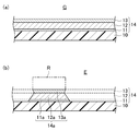
- FIG. 2 is a cross-sectional view showing a manufacturing process of a TFT substrate according to an embodiment of the present invention.
- FIG. 1 and 2 show an embodiment of a thin film transistor substrate and a method for manufacturing the same according to the present invention.
- FIG. 1 is a cross-sectional view of the TFT substrate 20 of the present embodiment.
- FIG. 2A is a cross-sectional view showing a conductive film forming step of the manufacturing method of the TFT substrate 20, and
- FIG. 2B is a cross-sectional view showing the etching step.
- the TFT substrate 20 includes an insulating substrate 10, a plurality of gate lines (not shown) provided on the insulating substrate 10 so as to extend in parallel with each other, and a direction orthogonal to each gate line.
- a plurality of source lines (not shown) provided so as to extend in parallel, a plurality of TFTs 5 provided for each intersection of each gate line and each source line, that is, each pixel, and each TFT 5 are covered.
- An interlayer insulating film 18 provided on the interlayer insulating film 18, a plurality of pixel electrodes 19 provided in a matrix on the interlayer insulating film 18, and an alignment film (not shown) provided so as to cover each pixel electrode 19. Yes.
- the TFT 5 includes a gate electrode 14 a provided on the insulating substrate 10, a gate insulating film 15 provided so as to cover the gate electrode 14 a, and a gate electrode 14 a on the gate insulating film 15.
- the semiconductor layer 16 provided in an island shape, and the source electrode 17a and the drain electrode 17b provided on the semiconductor layer 16 so as to overlap the gate electrode 14a and to face each other are provided.
- the gate electrode 14a is, for example, a protruding portion to the side of each of the gate lines, and is stacked on the third conductive layer 11a and the third conductive layer 11a provided on the insulating substrate 10 as shown in FIG.
- the first conductive layer 12a and the second conductive layer 13a stacked on the first conductive layer 12a are provided.
- the first conductive layer 12a has a relatively high etching rate with a weak acidic etchant containing nitric acid, acetic acid, phosphoric acid, and water
- the second conductive layer 13a and the third conductive layer 11a have their weak acid etching.
- the etching rate by the liquid is relatively low. Further, as shown in FIG.
- the first conductive layer 12 a and the third conductive layer 11 a are provided in a forward tapered shape whose cross-sectional shape increases toward the insulating substrate 10 side.
- the second conductive layer 13a is an oxide film, and as shown in FIG. 1, has a reverse taper shape whose cross-sectional shape decreases toward the insulating substrate 10 side.
- the semiconductor layer 16 is, for example, an intrinsic amorphous silicon layer (not shown) having a channel region, and an n + layer that is stacked so that the channel region is exposed in the intrinsic amorphous silicon layer and connected to the source electrode 17a and the drain electrode 17b. And an amorphous silicon layer (not shown).
- the source electrode 17a is, for example, a portion protruding to the side of each source line.
- the drain electrode 17 b is connected to the pixel electrode 19 through a contact hole formed in the interlayer insulating film 18.
- the TFT substrate 20 having the above configuration constitutes an active matrix driving type liquid crystal display panel together with a counter substrate disposed opposite to the TFT substrate 20 and a liquid crystal layer sealed between the two substrates.
- the manufacturing method of this embodiment includes a conductive film forming step and an etching step.
- a third conductive film 11 such as a titanium film (thickness of about 50 nm), an aluminum film (thickness) is formed on the entire substrate of the insulating substrate 10 such as a glass substrate by sputtering.
- argon gas for example, 770 sccm
- argon gas for example, 770 sccm
- water vapor for example, 20 sccm
- sccm means “standard cubic centimeters per minute” and is a unit indicating a flow rate (cc) per minute.
- an aluminum film is exemplified as the first conductive film 12, but a copper film, a titanium film, and a chromium film can be used as long as the etching rate is relatively higher than the material used for the second conductive film 13. Further, a silver film, an alloy film containing at least one constituent element of these films, or the like may be used.
- a titanium oxide film is exemplified as the second conductive film 13, but a tantalum oxide film and a chromium oxide film can be used as long as the etching rate is relatively low as compared with the material used for the first conductive film 12.
- a tungsten oxide film, an alloy oxide film containing at least one of constituent elements of these films, or the like may be used.
- a titanium film is exemplified as the third conductive film 11, but a tantalum film, a chromium film, and a tungsten film can be used as long as the etching rate is relatively low as compared with the material used for the first conductive film 12.
- An alloy film containing at least one of the constituent elements of these films may be used.
- the third conductive film 11 is provided in order to improve the adhesion between the glass insulating substrate 10 and the aluminum first conductive film 12.
- the second conductive film 13 includes an ITO (Indium Tin Oxide) gate terminal formed of the same material in the same layer as the pixel electrode 19 and an aluminum first conductive layer 12a at the end of each gate line. It is provided in order to suppress an electrical corrosion (electric corrosion) reaction between the two.
- ITO Indium Tin Oxide
- the resist pattern R is formed on the substrate on which the multilayer conductive film 14 has been formed using photolithography, and then the multilayer conductive film 14 exposed from the resist pattern R is exposed.
- the laminated conductive film 14 is patterned by etching with a weakly acidic etchant E containing nitric acid, acetic acid, phosphoric acid and water to form the gate electrode 14a and the gate line (etching step).
- a weakly acidic etchant E containing nitric acid, acetic acid, phosphoric acid and water to form the gate electrode 14a and the gate line (etching step).
- the first conductive film 12 and the third conductive film 11 are forward-tapered so that the cross-sectional shapes of the portions that become the gate electrodes 14 a and the gate lines increase toward the insulating substrate 10.
- the first conductive film 12 and the third conductive film 11 are patterned in a shape, and the cross-sectional shape of the portion of the second conductive film 13 that becomes the gate electrode 14a and the gate line becomes an inversely tapered shape that decreases toward the insulating substrate 10 side.
- the second conductive film 13 is patterned.
- a silicon nitride film (thickness of about 400 nm) is formed on the entire substrate on which the gate electrode 14a and the gate lines are formed by a plasma CVD (Chemical Vapor Deposition) method, and the gate insulating film 15 (FIG. 1). Reference).
- an intrinsic amorphous silicon film (thickness of about 100 nm) and an n + amorphous silicon film doped with phosphorus (thickness of about 50 nm) are formed on the entire substrate on which the gate insulating film 15 is formed by plasma CVD.
- the laminated layer of the intrinsic amorphous silicon film and the n + amorphous silicon film is patterned into an island shape on the gate electrode 14a using photolithography, thereby forming a semiconductor layer forming portion.
- an aluminum film (thickness of about 400 nm), a titanium film (thickness of about 50 nm), and the like are sequentially formed on the entire substrate on which the semiconductor layer forming portion is formed by a sputtering method.
- the metal laminated film is patterned using photolithography to form a source electrode 17a, a drain electrode 17b (see FIG. 1), and a source line.
- the n + amorphous silicon layer in the semiconductor layer forming portion is etched to form a channel region, thereby forming the semiconductor layer 16 and the TFT 5 including the same (see FIG. 1). ).
- a silicon nitride film (thickness of about 200 nm) or the like is formed on the entire substrate on which the TFT 5 is formed, thereby forming an inorganic insulating film.
- an acrylic photosensitive resin is applied to a thickness of about 2 ⁇ m by spin coating on the entire substrate on which the inorganic insulating film is formed, and the applied photosensitive resin is passed through a photomask. After the exposure, development is performed to form an organic insulating film having a contact hole on the drain electrode 17b (see FIG. 1).
- an interlayer insulating film 18 made of the inorganic insulating film and the organic insulating film is formed.
- the transparent conductive film is formed using photolithography.
- the pixel electrode 19 is formed by patterning.
- the TFT substrate 20 can be manufactured.
- the etching rate is relatively low. Since the low second conductive film 13 is formed in an atmosphere of process gas G containing water vapor, the entire second conductive film 13 can be formed of a uniform oxide film.
- the etching step when the gate electrode 14a is formed by patterning the laminated conductive film 14 by etching with the etchant E, that is, the second conductive film 13 is patterned by etching with the etchant E to form an upper layer of the gate electrode 14a.
- the film quality and etching rate of the second conductive film 13 are uniform along the thickness direction, even if the second conductive film 13 is patterned in a reverse taper shape, the peripheral edge of the surface layer is formed. It is difficult to form a hook-like protruding portion on the part. Accordingly, a ridge-like protruding portion is formed at the peripheral edge portion of the surface layer of the gate electrode 14a formed by patterning the laminated conductive film 14 composed of the third conductive film 11, the first conductive film 12, and the second conductive film 13. Therefore, it is possible to suppress the formation of a ridge-like protruding portion in the surface layer of the gate electrode 14a having a stacked structure.
- the TFT substrate 20 including the bottom gate type TFT 5 is illustrated, but the present invention can also be applied to a TFT substrate including the top gate type TFT.
- the gate electrode is exemplified as an object to suppress the formation of the hook-shaped protruding portion in the conductive member.
- the present invention is applicable to display wiring such as a gate line and a source line including the source electrode. Can also be applied.
- the TFT substrate 20 in which the electrode of the TFT 5 connected to the pixel electrode 19 is the drain electrode 17b is illustrated.
- the TFT electrode connected to the pixel electrode is referred to as a source electrode. It can also be applied to a substrate.
- the present invention is useful for a TFT substrate constituting a display panel of an active matrix driving system because formation of a ridge-like protruding portion is suppressed in the surface layer of a gate electrode having a laminated structure.
Landscapes
- Thin Film Transistor (AREA)
Abstract
エッチング液(E)によるエッチングレートが相対的に高い第1導電膜(12)、及びエッチング液(E)によるエッチングレートが相対的に低い第2導電膜(13)を基板(10)に順に成膜して、積層導電膜(14)を形成する導電膜成膜工程と、積層導電膜(14)をフォトリソグラフィ及びエッチング液(E)によるエッチングによってパターニングして、ゲート電極(14a)を形成するエッチング工程とを備えるTFT基板の製造方法であって、導電膜成膜工程では、水蒸気を含むプロセスガス(G)の雰囲気中で第2導電膜(13)を成膜する。
Description
本発明は、薄膜トランジスタ基板及びその製造方法に関し、特に、表示パネルを構成する薄膜トランジスタ基板及びその製造方法に関するものである。
アクティブマトリクス駆動方式の液晶表示パネルは、画像の最小単位である各画素毎に、スイッチング素子として、例えば、薄膜トランジスタ(Thin Film Transistor、以下、「TFT」とも称する)が設けられたTFT基板を備えている。
TFTは、例えば、ガラス基板上に設けられたゲート電極と、ゲート電極を覆うように設けられたゲート絶縁膜と、ゲート絶縁膜上にゲート電極に重なるように島状に設けられた半導体層と、半導体層上にゲート電極に重なると共に、互いに対峙するように設けられたソース電極及びドレイン電極とを備えている。ここで、ゲート電極、ソース電極及びドレイン電極などは、基板に複数の金属膜を連続的に成膜して金属積層膜を形成した後に、その金属積層膜をパターニングすることにより、形成される場合が多い。
例えば、特許文献1には、リン酸三アンモニウム三水和物、酢酸モノエタノールアミン塩、過酸化水素及び水を含有し、Cu又はCu合金とMo又はMo合金とからなる積層金属層のCu又はCu合金とMo又はMo合金とを一度にエッチングするためのエッチング組成物が開示されている。
ところで、TFTのゲート電極を形成するために、例えば、ガラス基板上に、スパッタリング法により、Ti膜、Al膜及びTi膜を連続的に成膜して、Ti/Al/Tiの金属積層膜を形成した後に、その金属積層膜をウエットエッチングによりパターニングすると、ゲート電極を構成する上層Tiの表層の周端部が庇状に側方に突出して形成されることがある。そうなると、例えば、上層Tiの庇状の突出部分にエッチャントなどが残留し易くなったり、上層Tiの庇状の突出部分が静電気放電の起点となったりするので、後に続く製造工程や製造されたTFT基板において、不具合が発生するおそれがある。ここで、上層Tiの表層の周端部が庇状に突出して形成される理由としては、上層Tiが実際にはチタン膜とその表層に形成された酸化チタン膜とにより構成され易く、例えば、硝酸、酢酸、リン酸及び水を含む弱酸性エッチング液などのTi/Al/Tiの金属積層膜を一度にエッチング可能なエッチャントにおいて、表層の酸化チタン膜がその下層のチタン膜よりもエッチングされ難いことが考えられる。
本発明は、かかる点に鑑みてなされたものであり、その目的とするところは、積層構造を有するゲート電極の表層において、庇状の突出部分の形成を抑制することにある。
上記目的を達成するために、本発明は、エッチングレートが相対的に低いゲート電極の上層側を形成するための第2導電膜が酸化膜により構成されるようにしたものである。
具体的に本発明に係る薄膜トランジスタ基板の製造方法は、エッチング液によるエッチングレートが相対的に高い第1導電膜、及び該エッチングレートが相対的に低い第2導電膜を基板に順に成膜して、積層導電膜を形成する導電膜成膜工程と、上記積層導電膜をフォトリソグラフィ及び上記エッチング液によるエッチングによってパターニングして、ゲート電極を形成するエッチング工程とを備える薄膜トランジスタ基板の製造方法であって、上記導電膜成膜工程では、水蒸気を含むプロセスガスの雰囲気中で上記第2導電膜を成膜することを特徴とする。
上記の方法によれば、導電膜成膜工程では、エッチングレートが相対的に高い第1導電膜を成膜した後に、エッチングレートが相対的に低い第2導電膜を水蒸気を含むプロセスガスの雰囲気中で成膜するので、第2導電膜の全体が均一な酸化膜により構成される。そして、エッチング工程において、積層導電膜をエッチング液によるエッチングによってパターニングしてゲート電極を形成する際、すなわち、第2導電膜をエッチング液によるエッチングによってパターニングしてゲート電極の上層側を形成する際には、第2導電膜の膜質及びエッチングレートが厚さ方向に沿って均一であるので、第2導電膜が逆テーパー状にパターニングされても、その表層の周端部には、庇状の突出部分が形成され難くなる。したがって、第1導電膜及び第2導電膜からなる積層導電膜をパターニングして形成されるゲート電極の表層の周端部において、庇状の突出部分が形成され難いので、積層構造を有するゲート電極の表層において、庇状の突出部分の形成が抑制される。
上記第1導電膜は、アルミニウム膜であり、上記第2導電膜は、酸化チタン膜であってもよい。
上記の方法によれば、第1導電膜がアルミニウム膜であり、第2導電膜が酸化チタン膜であるので、例えば、硝酸、酢酸、リン酸及び水を含む弱酸性エッチング液において、第1導電膜のエッチングレートが具体的に相対的に高くなり、第2導電膜のエッチングレートが具体的に相対的に低くなる。
上記導電膜成膜工程では、上記第1導電膜を成膜する前に、該第1導電膜と上記基板との密着性を向上させるための第3導電膜を成膜してもよい。
上記の方法によれば、導電膜成膜工程において、第3導電膜、第1導電膜及び第2導電膜を基板に順に成膜することにより、第2導電膜(上層)/第1導電膜(中層)/第3導電膜(下層)の3層積層構造を有する積層導電膜が形成されるので、基板と積層導電膜との密着性が第3導電膜を介して向上する。
上記第3導電膜は、チタン膜であってもよい。
上記の方法によれば、第3導電膜がチタン膜であるので、例えば、ガラス基板と積層導電膜との密着性が具体的に向上する。
上記エッチング工程では、上記ゲート電極の上記第1導電膜に対応する部分の断面形状が上記基板側に向かって大きくなる順テーパー形状に該第1導電膜をパターニングすると共に、上記ゲート電極の上記第2導電膜に対応する部分の断面形状が上記基板側に向かって小さくなる逆テーパー形状に該第2導電膜をパターニングしてもよい。
上記の方法によれば、エッチング工程において、第1導電膜を順テーパー形状にパターニングすると共に、第2導電膜を逆テーパー形状にパターニングするので、例えば、硝酸、酢酸、リン酸及び水を含む弱酸性エッチング液を用いて、酸化チタン層(上層)/アルミニウム層(下層)の積層構造を有するゲート電極が具体的に形成される。
また、本発明に係る薄膜トランジスタ基板は、エッチング液によるエッチングレートが相対的に高い第1導電層、及び該第1導電層上に設けられ、該エッチングレートが相対的に低い第2導電層を有するゲート電極が基板に設けられた薄膜トランジスタ基板であって、上記第2導電層は、酸化膜であることを特徴とする。
上記の構成によれば、第2導電層が酸化膜であるので、例えば、第2導電層となる第2導電膜の全体が均一な酸化膜により構成されることになる。そして、第2導電膜をエッチング液によるエッチングによってパターニングしてゲート電極の上層側を形成する際には、第2導電膜の膜質及びエッチングレートが厚さ方向に沿って均一になっているので、第2導電膜が逆テーパー状にパターニングされても、その表層の周端部には、庇状の突出部分が形成され難い。したがって、第1導電層及び第2導電層からなるゲート電極の表層の周端部において、庇状の突出部分が形成され難いので、積層構造を有するゲート電極の表層において、庇状の突出部分の形成が抑制される。
上記第1導電層は、断面形状が上記基板側に向かって大きくなる順テーパー形状に設けられ、上記第2導電層は、断面形状が上記基板側に向かって小さくなる逆テーパー形状に設けられていてもよい。
上記の構成によれば、第1導電層の断面形状が基板側に向かって大きくなる順テーパー形状に設けられ、第2導電層の断面形状が基板側に向かって小さくなる逆テーパー形状に設けられているので、例えば、硝酸、酢酸、リン酸及び水を含む弱酸性エッチング液を用いて、酸化チタン層からなる第2導電層(上層)/アルミニウム層からなる第1導電層(下層)の積層構造を有するゲート電極が具体的に構成される。
本発明によれば、エッチングレートが相対的に低いゲート電極の上層側を形成するための第2導電膜が酸化膜により構成されるので、積層構造を有するゲート電極の表層において、庇状の突出部分の形成を抑制することができる。
以下、本発明の実施形態を図面に基づいて詳細に説明する。なお、本発明は、以下の実施形態に限定されるものではない。
図1及び図2は、本発明に係る薄膜トランジスタ基板及びその製造方法の一実施形態を示している。具体的に図1は、本実施形態のTFT基板20の断面図である。また、図2(a)は、TFT基板20の製造方法の導電膜成膜工程を示す断面図であり、図2(b)は、そのエッチング工程を示す断面図である。
TFT基板20は、図1に示すように、絶縁基板10と、絶縁基板10上に互いに平行に延びるように設けられた複数のゲート線(不図示)と、各ゲート線と直交する方向に互いに平行に延びるように設けられた複数のソース線(不図示)と、各ゲート線及び各ソース線の交差部分毎、すなわち、各画素毎にそれぞれ設けられた複数のTFT5と、各TFT5を覆うように設けられた層間絶縁膜18と、層間絶縁膜18上にマトリクス状に設けられた複数の画素電極19と、各画素電極19を覆うように設けられた配向膜(不図示)とを備えている。
TFT5は、図1に示すように、絶縁基板10上に設けられたゲート電極14aと、ゲート電極14aを覆うように設けられたゲート絶縁膜15と、ゲート絶縁膜15上にゲート電極14aに重なるように島状に設けられた半導体層16と、半導体層16上にゲート電極14aに重なると共に互いに対峙するように設けられたソース電極17a及びドレイン電極17bとを備えている。
ゲート電極14aは、例えば、上記各ゲート線の側方への突出部分であり、図1に示すように、絶縁基板10上に設けられた第3導電層11aと、第3導電層11aに積層された第1導電層12aと、第1導電層12aに積層された第2導電層13aとを備えている。ここで、第1導電層12aは、硝酸、酢酸、リン酸及び水を含む弱酸性エッチング液によるエッチングレートが相対的に高く、第2導電層13a及び第3導電層11aは、その弱酸性エッチング液によるエッチングレートが相対的に低くなっている。また、第1導電層12a及び第3導電層11aは、図1に示すように、その断面形状が絶縁基板10側に向かって大きくなる順テーパー形状に設けられている。さらに、第2導電層13aは、酸化膜であり、図1に示すように、その断面形状が絶縁基板10側に向かって小さくなる逆テーパー形状に設けられている。
半導体層16は、例えば、チャネル領域を有する真性アモルファスシリコン層(不図示)と、真性アモルファスシリコン層にそのチャネル領域が露出するように積層され、ソース電極17a及びドレイン電極17bに接続されたn+アモルファスシリコン層(不図示)とを備えている。
ソース電極17aは、例えば、上記各ソース線の側方への突出した部分である。
ドレイン電極17bは、図1に示すように、層間絶縁膜18に形成されたコンタクトホールを介して画素電極19に接続されている。
上記構成のTFT基板20は、それに対向して配置される対向基板と、それらの両基板の間に封入される液晶層と共に、アクティブマトリクス駆動方式の液晶表示パネルを構成するものである。
次に、本実施形態のTFT基板20を製造する方法について、図1及び図2を用いて説明する。ここで、本実施形態の製造方法は、導電膜成膜工程及びエッチング工程を備える。
まず、ガラス基板などの絶縁基板10の基板全体に、図2(a)に示すように、スパッタリング法により、例えば、チタン膜(厚さ50nm程度)などの第3導電膜11、アルミニウム膜(厚さ400nm程度)などの第1導電膜12、及び酸化チタン膜(厚さ150nm程度)などの第2導電膜12を順に成膜して、積層導電膜14を形成する(導電膜成膜工程)。ここで、チタン膜を成膜する際には、チタンターゲットが内部に配置された処理室の内部にプロセスガスとしてアルゴンガス(例えば、770sccm)を導入し、酸化チタン膜を成膜する際には、その処理室の内部にアルゴンガス(例えば、770sccm)及び水蒸気(例えば、20sccm)を導入して、処理室の内部を水蒸気を含むプロセスガスGの雰囲気にする。なお、sccmは、「standard cubic centimeters per minute」という意味であり、1分間当たり流量(cc)を示す単位である。また、本実施形態では、第1導電膜12として、アルミニウム膜を例示したが、第2導電膜13に用いる材料と比較して相対的にエッチングレートが高ければ、銅膜、チタン膜、クロム膜、銀膜、それらの膜の構成元素を少なくとも1つを含む合金膜などであってもよい。また、本実施形態では、第2導電膜13として、酸化チタン膜を例示したが、第1導電膜12に用いる材料と比較して相対的にエッチングレートが低ければ、酸化タンタル膜、酸化クロム膜、酸化タングステン膜、それらの膜の構成元素を少なくとも1つを含む合金酸化膜などであってもよい。また、本実施形態では、第3導電膜11として、チタン膜を例示したが、第1導電膜12に用いる材料と比較して相対的にエッチングレートが低ければ、タンタル膜、クロム膜、タングステン膜、それらの膜の構成元素を少なくとも1つを含む合金膜などであってもよい。さらに、第3導電膜11は、ガラス製の絶縁基板10とアルミニウム製の第1導電膜12との密着性を向上させるために設けられている。また、第2導電膜13は、上記各ゲート線の端部に、画素電極19と同一層に同一材料により形成されたITO(Indium Tin Oxide)製のゲート端子とアルミニウム製の第1導電層12aとの間の電気的な腐食(電蝕)反応を抑制するために設けられている。
続いて、図2(b)に示すように、積層導電膜14が形成された基板上に、フォトリソグラフィを用いてレジストパターンRを形成した後に、レジストパターンRから露出する積層導電膜14に対して、硝酸、酢酸、リン酸及び水を含む弱酸性エッチング液Eによるエッチングを行うことにより、積層導電膜14をパターニングして、ゲート電極14a及びゲート線を形成する(エッチング工程)。ここで、積層導電膜14をパターニングする際には、第1導電膜12及び第3導電膜11のゲート電極14a及びゲート線となる部分の断面形状が絶縁基板10側に向かって大きくなる順テーパー形状に第1導電膜12及び第3導電膜11をパターニングすると共に、第2導電膜13のゲート電極14a及びゲート線となる部分の断面形状が絶縁基板10側に向かって小さくなる逆テーパー形状に第2導電膜13をパターニングすることになる。
その後、ゲート電極14a及びゲート線が形成された基板全体に、プラズマCVD(Chemical Vapor Deposition)法により、例えば、窒化シリコン膜(厚さ400nm程度)などを成膜し、ゲート絶縁膜15(図1参照)を形成する。
さらに、ゲート絶縁膜15が形成された基板全体に、プラズマCVD法により、例えば、真性アモルファスシリコン膜(厚さ100nm程度)、及びリンがドープされたn+アモルファスシリコン膜(厚さ50nm程度)を順に成膜した後に、真性アモルファスシリコン膜及びn+アモルファスシリコン膜の積層膜をフォトリソグラフィを用いてゲート電極14a上に島状にパターニングすることにより、半導体層形成部を形成する。
引き続いて、上記半導体層形成部が形成された基板全体に、スパッタリング法により、例えば、アルミニウム膜(厚さ400nm程度)及びチタン膜(厚さ50nm程度)などを順に成膜して、金属積層膜を形成した後に、その金属積層膜をフォトリソグラフィを用いてパターニングすることにより、ソース電極17a及びドレイン電極17b(図1参照)並びにソース線を形成する。
そして、ソース電極17a及びドレイン電極17bをマスクとして、上記半導体層形成部のn+アモルファスシリコン層をエッチングすることにより、チャネル領域を形成して、半導体層16及びそれを備えたTFT5(図1参照)を形成する。
さらに、TFT5が形成された基板全体に、例えば、窒化シリコン膜(厚さ200nm程度)などを成膜し、無機絶縁膜を形成する。
続いて、上記無機絶縁膜が形成された基板全体に、スピンコート法により、例えば、アクリル系の感光性樹脂を厚さ2μm程度に塗布し、その塗布された感光性樹脂をフォトマスクを介して露光した後に、現像することにより、ドレイン電極17b(図1参照)上にコンタクトホールを有する有機絶縁膜を形成する。
さらに、上記有機絶縁膜のコンタクトホールから露出する上記無機絶縁膜をエッチングすることにより、無機絶縁膜及び有機絶縁膜からなる層間絶縁膜18(図1参照)を形成する。
最後に、層間絶縁膜18が形成された基板全体に、スパッタリング法により、例えば、ITO膜(厚さ100nm程度)などの透明導電膜を成膜した後に、その透明導電膜をフォトリソグラフィを用いてパターニングすることにより、画素電極19を形成する。
以上のようにして、TFT基板20を製造することができる。
以上説明したように、本実施形態のTFT基板20及びその製造方法によれば、導電膜成膜工程において、エッチングレートが相対的に高い第1導電膜12を成膜した後に、エッチングレートが相対的に低い第2導電膜13を水蒸気を含むプロセスガスGの雰囲気中で成膜するので、第2導電膜13の全体を均一な酸化膜により構成することができる。そして、エッチング工程において、積層導電膜14をエッチング液Eによるエッチングによってパターニングしてゲート電極14aを形成する際、すなわち、第2導電膜13をエッチング液Eによるエッチングによってパターニングしてゲート電極14aの上層側を形成する際には、第2導電膜13の膜質及びエッチングレートが厚さ方向に沿って均一であるので、第2導電膜13が逆テーパー状にパターニングされても、その表層の周端部には、庇状の突出部分が形成され難くなる。したがって、第3導電膜11、第1導電膜12及び第2導電膜13からなる積層導電膜14をパターニングして形成されるゲート電極14aの表層の周端部において、庇状の突出部分が形成され難いので、積層構造を有するゲート電極14aの表層において、庇状の突出部分の形成を抑制することができる。
なお、本実施形態では、ボトムゲート型のTFT5を備えたTFT基板20を例示したが、本発明は、トップゲート型のTFTを備えたTFT基板にも適用することができる。
また、本実施形態では、導電部材における庇状の突出部分の形成が抑制される対象として、ゲート電極を例示したが、本発明は、ゲート線やソース電極を含むソース線などの表示用配線にも適用することができる。
また、本実施形態では、画素電極19に接続されたTFT5の電極をドレイン電極17bとしたTFT基板20を例示したが、本発明は、画素電極に接続されたTFTの電極をソース電極と呼ぶTFT基板にも適用することができる。
以上説明したように、本発明は、積層構造を有するゲート電極の表層において、庇状の突出部分の形成が抑制されるので、アクティブマトリクス駆動方式の表示パネルを構成するTFT基板について有用である。
E エッチング液
G プロセスガス
10 絶縁基板
11 第3導電膜
12 第1導電膜
12a 第1導電層
13 第2導電膜
13a 第2導電層
14 積層導電膜
14a ゲート電極
20 TFT基板
G プロセスガス
10 絶縁基板
11 第3導電膜
12 第1導電膜
12a 第1導電層
13 第2導電膜
13a 第2導電層
14 積層導電膜
14a ゲート電極
20 TFT基板
Claims (7)
- エッチング液によるエッチングレートが相対的に高い第1導電膜、及び該エッチングレートが相対的に低い第2導電膜を基板に順に成膜して、積層導電膜を形成する導電膜成膜工程と、
上記積層導電膜をフォトリソグラフィ及び上記エッチング液によるエッチングによってパターニングして、ゲート電極を形成するエッチング工程とを備える薄膜トランジスタ基板の製造方法であって、
上記導電膜成膜工程では、水蒸気を含むプロセスガスの雰囲気中で上記第2導電膜を成膜することを特徴とする薄膜トランジスタ基板の製造方法。 - 請求項1に記載された薄膜トランジスタ基板の製造方法において、
上記第1導電膜は、アルミニウム膜であり、
上記第2導電膜は、酸化チタン膜であることを特徴とする薄膜トランジスタ基板の製造方法。 - 請求項1又は2に記載された薄膜トランジスタ基板の製造方法において、
上記導電膜成膜工程では、上記第1導電膜を成膜する前に、該第1導電膜と上記基板との密着性を向上させるための第3導電膜を成膜することを特徴とする薄膜トランジスタ基板の製造方法。 - 請求項3に記載された薄膜トランジスタ基板の製造方法において、
上記第3導電膜は、チタン膜であることを特徴とする薄膜トランジスタ基板の製造方法。 - 請求項1乃至4の何れか1つに記載された薄膜トランジスタ基板の製造方法において、
上記エッチング工程では、上記ゲート電極の上記第1導電膜に対応する部分の断面形状が上記基板側に向かって大きくなる順テーパー形状に該第1導電膜をパターニングすると共に、上記ゲート電極の上記第2導電膜に対応する部分の断面形状が上記基板側に向かって小さくなる逆テーパー形状に該第2導電膜をパターニングすることを特徴とする薄膜トランジスタ基板の製造方法。 - エッチング液によるエッチングレートが相対的に高い第1導電層、及び該第1導電層上に設けられ、該エッチングレートが相対的に低い第2導電層を有するゲート電極が基板に設けられた薄膜トランジスタ基板であって、
上記第2導電層は、酸化膜であることを特徴とする薄膜トランジスタ基板。 - 請求項6に記載された薄膜トランジスタ基板において、
上記第1導電層は、断面形状が上記基板側に向かって大きくなる順テーパー形状に設けられ、
上記第2導電層は、断面形状が上記基板側に向かって小さくなる逆テーパー形状に設けられていることを特徴とする薄膜トランジスタ基板。
Applications Claiming Priority (2)
| Application Number | Priority Date | Filing Date | Title |
|---|---|---|---|
| JP2010045091 | 2010-03-02 | ||
| JP2010-045091 | 2010-03-02 |
Publications (1)
| Publication Number | Publication Date |
|---|---|
| WO2011108050A1 true WO2011108050A1 (ja) | 2011-09-09 |
Family
ID=44541736
Family Applications (1)
| Application Number | Title | Priority Date | Filing Date |
|---|---|---|---|
| PCT/JP2010/007225 Ceased WO2011108050A1 (ja) | 2010-03-02 | 2010-12-13 | 薄膜トランジスタ基板及びその製造方法 |
Country Status (1)
| Country | Link |
|---|---|
| WO (1) | WO2011108050A1 (ja) |
Cited By (2)
| Publication number | Priority date | Publication date | Assignee | Title |
|---|---|---|---|---|
| WO2017090524A1 (ja) * | 2015-11-27 | 2017-06-01 | シャープ株式会社 | ウェットエッチング方法、及び半導体装置の製造方法 |
| CN109087852A (zh) * | 2018-08-10 | 2018-12-25 | 深圳市华星光电技术有限公司 | 晶体管金属电极结构的制作方法 |
Citations (8)
| Publication number | Priority date | Publication date | Assignee | Title |
|---|---|---|---|---|
| JPH06177381A (ja) * | 1992-12-03 | 1994-06-24 | Fujitsu Ltd | 薄膜トランジスタマトリクスおよびその製造方法 |
| JP2000047263A (ja) * | 1998-07-31 | 2000-02-18 | Fujitsu Ltd | エッチング方法、薄膜トランジスタマトリックス基板、およびその製造方法 |
| JP2000171834A (ja) * | 1998-10-02 | 2000-06-23 | Hitachi Ltd | 液晶表示装置とその製造方法 |
| JP2002009061A (ja) * | 2000-06-23 | 2002-01-11 | Nec Kagoshima Ltd | ウェットエッチング方法 |
| JP2005044851A (ja) * | 2003-07-23 | 2005-02-17 | Seiko Epson Corp | 薄膜半導体素子、及び薄膜半導体素子の製造方法 |
| JP2005316399A (ja) * | 2004-02-19 | 2005-11-10 | Sharp Corp | 導電素子基板の製造方法、導電素子基板、液晶表示装置の製造方法、液晶表示装置、及び電子情報機器 |
| JP2007294928A (ja) * | 2006-03-31 | 2007-11-08 | Semiconductor Energy Lab Co Ltd | 半導体装置 |
| JP2009016756A (ja) * | 2007-07-09 | 2009-01-22 | Nec Lcd Technologies Ltd | アクティブマトリクス駆動表示装置 |
-
2010
- 2010-12-13 WO PCT/JP2010/007225 patent/WO2011108050A1/ja not_active Ceased
Patent Citations (8)
| Publication number | Priority date | Publication date | Assignee | Title |
|---|---|---|---|---|
| JPH06177381A (ja) * | 1992-12-03 | 1994-06-24 | Fujitsu Ltd | 薄膜トランジスタマトリクスおよびその製造方法 |
| JP2000047263A (ja) * | 1998-07-31 | 2000-02-18 | Fujitsu Ltd | エッチング方法、薄膜トランジスタマトリックス基板、およびその製造方法 |
| JP2000171834A (ja) * | 1998-10-02 | 2000-06-23 | Hitachi Ltd | 液晶表示装置とその製造方法 |
| JP2002009061A (ja) * | 2000-06-23 | 2002-01-11 | Nec Kagoshima Ltd | ウェットエッチング方法 |
| JP2005044851A (ja) * | 2003-07-23 | 2005-02-17 | Seiko Epson Corp | 薄膜半導体素子、及び薄膜半導体素子の製造方法 |
| JP2005316399A (ja) * | 2004-02-19 | 2005-11-10 | Sharp Corp | 導電素子基板の製造方法、導電素子基板、液晶表示装置の製造方法、液晶表示装置、及び電子情報機器 |
| JP2007294928A (ja) * | 2006-03-31 | 2007-11-08 | Semiconductor Energy Lab Co Ltd | 半導体装置 |
| JP2009016756A (ja) * | 2007-07-09 | 2009-01-22 | Nec Lcd Technologies Ltd | アクティブマトリクス駆動表示装置 |
Cited By (5)
| Publication number | Priority date | Publication date | Assignee | Title |
|---|---|---|---|---|
| WO2017090524A1 (ja) * | 2015-11-27 | 2017-06-01 | シャープ株式会社 | ウェットエッチング方法、及び半導体装置の製造方法 |
| CN108352315A (zh) * | 2015-11-27 | 2018-07-31 | 夏普株式会社 | 湿蚀刻方法及半导体装置的制造方法 |
| JPWO2017090524A1 (ja) * | 2015-11-27 | 2018-08-30 | シャープ株式会社 | ウェットエッチング方法、及び半導体装置の製造方法 |
| CN109087852A (zh) * | 2018-08-10 | 2018-12-25 | 深圳市华星光电技术有限公司 | 晶体管金属电极结构的制作方法 |
| CN109087852B (zh) * | 2018-08-10 | 2020-09-08 | 深圳市华星光电技术有限公司 | 晶体管金属电极结构的制作方法 |
Similar Documents
| Publication | Publication Date | Title |
|---|---|---|
| US8497966B2 (en) | FFS type TFT-LCD array substrate and manufacturing method thereof | |
| KR101325053B1 (ko) | 박막 트랜지스터 기판 및 이의 제조 방법 | |
| JP5588740B2 (ja) | Tft−lcdアレイ基板およびその製造方法 | |
| EP2565917B1 (en) | Manufacturing method for array substrate with fringe field switching type thin film transistor liquid crystal display | |
| CN102768992B (zh) | 一种薄膜晶体管驱动背板的制作方法 | |
| US9613986B2 (en) | Array substrate and its manufacturing method, display device | |
| US20140061635A1 (en) | Array Substrate, Manufacturing Method And The Display Device Thereof | |
| EP2804207A1 (en) | Method for manufacturing tft array substrate | |
| JP2007212699A (ja) | 反射型tft基板及び反射型tft基板の製造方法 | |
| JP2007157916A (ja) | Tft基板及びtft基板の製造方法 | |
| CN105070684B (zh) | 阵列基板的制备方法、阵列基板及显示装置 | |
| US9379147B2 (en) | Thin-film transistor array substrate and manufacturing method thereof | |
| US9372378B2 (en) | TFT-LCD array substrate and method of manufacturing the same | |
| CN103489877A (zh) | 阵列基板及其制造方法和显示装置 | |
| US9716117B2 (en) | Method for producing a via, a method for producing an array substrate, an array substrate, and a display device | |
| TW200529451A (en) | Liquid crystal display unit | |
| KR20080084084A (ko) | 박막트랜지스터와 이를 포함하는 액정표시장치용 어레이기판의 제조방법 | |
| WO2014042058A1 (ja) | 回路基板、その製造方法及び表示装置 | |
| US20150221677A1 (en) | Active matrix substrate, display device, and production method therefor | |
| CN103311182B (zh) | 制造用于面内切换模式液晶显示器装置的阵列基板的方法 | |
| CN104681626A (zh) | 氧化物薄膜晶体管及其制作方法、阵列基板 | |
| WO2011108050A1 (ja) | 薄膜トランジスタ基板及びその製造方法 | |
| JP5707725B2 (ja) | 薄膜のパターニング方法及び表示パネルの製造方法 | |
| US20130323470A1 (en) | Conductive structure for panel and manufacturing method thereof | |
| US8647980B2 (en) | Method of forming wiring and method of manufacturing semiconductor substrates |
Legal Events
| Date | Code | Title | Description |
|---|---|---|---|
| 121 | Ep: the epo has been informed by wipo that ep was designated in this application |
Ref document number: 10846957 Country of ref document: EP Kind code of ref document: A1 |
|
| NENP | Non-entry into the national phase |
Ref country code: DE |
|
| 122 | Ep: pct application non-entry in european phase |
Ref document number: 10846957 Country of ref document: EP Kind code of ref document: A1 |
|
| NENP | Non-entry into the national phase |
Ref country code: JP |