WO2011105408A1 - Processeur simd - Google Patents
Processeur simd Download PDFInfo
- Publication number
- WO2011105408A1 WO2011105408A1 PCT/JP2011/053935 JP2011053935W WO2011105408A1 WO 2011105408 A1 WO2011105408 A1 WO 2011105408A1 JP 2011053935 W JP2011053935 W JP 2011053935W WO 2011105408 A1 WO2011105408 A1 WO 2011105408A1
- Authority
- WO
- WIPO (PCT)
- Prior art keywords
- instruction
- pes
- simd
- simd processor
- data
- Prior art date
Links
- 238000012545 processing Methods 0.000 claims abstract description 16
- 238000012546 transfer Methods 0.000 claims description 7
- 239000013256 coordination polymer Substances 0.000 claims 7
- 238000000034 method Methods 0.000 description 10
- 230000000694 effects Effects 0.000 description 7
- 238000011161 development Methods 0.000 description 6
- 238000010586 diagram Methods 0.000 description 5
- 101100243454 Caenorhabditis elegans pes-10 gene Proteins 0.000 description 4
- 101100136062 Mycobacterium tuberculosis (strain ATCC 25618 / H37Rv) PE10 gene Proteins 0.000 description 4
- 230000008859 change Effects 0.000 description 4
- 230000008569 process Effects 0.000 description 3
- 238000004364 calculation method Methods 0.000 description 2
- 230000008878 coupling Effects 0.000 description 2
- 238000010168 coupling process Methods 0.000 description 2
- 238000005859 coupling reaction Methods 0.000 description 2
- 230000006872 improvement Effects 0.000 description 2
- 101000741396 Chlamydia muridarum (strain MoPn / Nigg) Probable oxidoreductase TC_0900 Proteins 0.000 description 1
- 101000741399 Chlamydia pneumoniae Probable oxidoreductase CPn_0761/CP_1111/CPj0761/CpB0789 Proteins 0.000 description 1
- 101000741400 Chlamydia trachomatis (strain D/UW-3/Cx) Probable oxidoreductase CT_610 Proteins 0.000 description 1
- 101100136063 Mycobacterium tuberculosis (strain ATCC 25618 / H37Rv) PE11 gene Proteins 0.000 description 1
- 230000004913 activation Effects 0.000 description 1
- 230000002457 bidirectional effect Effects 0.000 description 1
- 230000006870 function Effects 0.000 description 1
- 238000013507 mapping Methods 0.000 description 1
- 230000007246 mechanism Effects 0.000 description 1
- 238000012986 modification Methods 0.000 description 1
- 230000004048 modification Effects 0.000 description 1
Images

Classifications
-
- G—PHYSICS
- G06—COMPUTING; CALCULATING OR COUNTING
- G06F—ELECTRIC DIGITAL DATA PROCESSING
- G06F15/00—Digital computers in general; Data processing equipment in general
- G06F15/76—Architectures of general purpose stored program computers
- G06F15/80—Architectures of general purpose stored program computers comprising an array of processing units with common control, e.g. single instruction multiple data processors
- G06F15/8007—Architectures of general purpose stored program computers comprising an array of processing units with common control, e.g. single instruction multiple data processors single instruction multiple data [SIMD] multiprocessors
-
- G—PHYSICS
- G06—COMPUTING; CALCULATING OR COUNTING
- G06F—ELECTRIC DIGITAL DATA PROCESSING
- G06F9/00—Arrangements for program control, e.g. control units
- G06F9/06—Arrangements for program control, e.g. control units using stored programs, i.e. using an internal store of processing equipment to receive or retain programs
- G06F9/30—Arrangements for executing machine instructions, e.g. instruction decode
- G06F9/38—Concurrent instruction execution, e.g. pipeline, look ahead
- G06F9/3885—Concurrent instruction execution, e.g. pipeline, look ahead using a plurality of independent parallel functional units
- G06F9/3887—Concurrent instruction execution, e.g. pipeline, look ahead using a plurality of independent parallel functional units controlled by a single instruction for multiple data lanes [SIMD]
Definitions
- the present invention relates to a SIMD (Single Instruction Multiple Data) processor.
- SIMD Single Instruction Multiple Data
- FIG. 9 is a diagram showing the configuration of the SIMD processor described in Non-Patent Document 1.
- the SIMD processor includes a plurality of computing elements (PE: Processing Element) 110 and a control processor (CP: Control Processor) 130 that issues the same instruction to the plurality of PEs 110.
- PE Processing Element
- CP Control Processor
- high computing performance can be realized based on inexpensive hardware.
- the data arranged at a predetermined position on the global memory (Global Memory) 140 managed by the CP 130 is sequentially read into the local memory (Local Memory) 120 on the PE 110 side in the order of addresses. Thereafter, all the PEs 110 perform calculations on the data in their local memory 120 at the same time in accordance with instructions issued from the CP 130.
- Patent Document 1 describes an image processor that can switch between a SIMD type and a systolic array type configuration.
- a dynamically reconfigurable processor As described above, a method of connecting a large number of memory blocks and a large number of PEs with abundant wiring (for example, crossbars) can be considered. However, according to this method, since it is necessary to add a large number of wiring circuits to the SIMD processor, hardware for realizing the SIMD processor becomes expensive.
- An object of the present invention is to provide a SIMD processor that solves such problems.
- the SIMD processor is: A SIMD (Single Instruction Multiple Data) processor comprising a control processor (CP: Control Processor) and a plurality of computing elements (PE: Processing Element), The plurality of PEs perform a SIMD operation to execute a single instruction issued from the CP, The CP performs a command / data distribution operation for distributing different commands or different commands and data to each of the plurality of PEs, Each of the plurality of PEs performs a systolic operation of executing an instruction sent from the CP in the instruction / data distribution operation after the source operands of the instruction are prepared.
- CP Control Processor
- PE Processing Element
- the SIMD processor According to the SIMD processor according to the present invention, it is possible to process a program at high speed by utilizing the arithmetic elements of the SIMD processor without changing the data arrangement on the global memory.
- the SIMD processor according to the first viewpoint is provided.
- the CP is provided with a SIMD processor that sequentially and exclusively uses instruction issue paths for all PEs in order to distribute instructions to each PE in the instruction / data distribution operation.
- the plurality of PEs transfer the operation results of the executed operation instructions to other PEs, and the operation results transferred from the other PEs are
- a SIMD processor is provided that serves as a source operand for instructions sent in an instruction / data distribution operation.
- each of the plurality of PEs uses the data sent from the CP as a source operand for the instruction sent in the command / data distribution operation. Is provided.
- a global access arbitration unit (Global Access Arbiter) that arbitrates global memory access by each of the plurality of PEs and guarantees access exclusiveness to the global memory is further provided.
- a SIMD processor is provided.
- a SIMD processor in which each of the plurality of PEs includes a register for storing a flag for keeping the operation stopped during the instruction / data distribution operation.
- a SIMD processor in which each of the plurality of PEs includes a register that stores a flag for switching the operation between the SIMD operation and the systolic operation.
- a SIMD processor in which each of the plurality of PEs includes a selector that selects whether or not to store an instruction issued from the CP in its own instruction buffer.
- the SIMD processor performs SIMD operation in which the entire PE array executes a single instruction issued from the control processor (CP), and the CP uses the instruction issue path to transmit different instruction codes and data.
- the instruction / data distribution operation to be sequentially transmitted to each PE is performed, and each PE in the PE array receives the instruction transmitted from the CP by the instruction / data distribution operation, not the instruction broadcast from the CP every cycle.
- a systolic operation is performed to specify that the execution result of the instruction is written to the register resource of another designated PE.
- each PE starts executing the instruction after the operands of the instruction are written by data sent from other PEs or CPs. It is sent to another PE, and in the case of a memory access command, the global memory is accessed.
- the SIMD processor of the present invention different instructions can be issued to each PE by the instruction / data distribution operation. Accordingly, it is possible to shift the timing of executing the memory access instruction between the PEs, or to allow only a specific PE to execute the memory access instruction. At this time, even if the data arrangement on the memory is left as it is and the memory space accessible by the PE is expanded to the global memory space, there are a number of cases when using the global memory space that is a single hardware resource. The frequency of competing PEs can be reduced, and the processing performance of the processing resources of the processor can be improved.
- the SIMD processor according to the present invention it is possible to speed up the processing using the operation resource of the SIMD processor without changing the data arrangement on the memory of the program (first effect).
- the CP performs an instruction / data distribution operation on the PE array, so that each arithmetic instruction corresponding to each arithmetic node and related constant data when processing for one iteration is expressed as a data flow graph It is possible to distribute to each PE and assign each operation node in the data flow graph to each PE. Further, in order for the CP to start execution in the systolic operation mode in the PE array, the activation data is repeatedly issued to one or more PEs, thereby starting up the different iterations one after another. The array can be processed.
- the processing for the portion (parallel loop portion) having no data dependency among the iterations in the loop portion of the program can be performed without changing the data arrangement on the global memory.
- the speed can be increased (second effect).
- the circuit resources of the instruction issue path to all PEs provided in the conventional SIMD processor and the data wiring circuit resources from each PE to the CP and from the CP to each PE are allocated. It can be used as it is. Further, as a connection for accessing the global memory space from each PE, a wiring circuit resource for exchanging scalar data between a CP and a PE array provided in a conventional SIMD processor can be used as it is. Furthermore, between PEs that perform operations in which operation nodes on the data flow graph transmit / receive data to / from each other, as a connection between PEs for transmitting / receiving data, the wiring resources between adjacent PEs provided in the conventional SIMD processor are used as they are. Can be used.
- the first effect and the second effect can be obtained (third effect) only by adding a small amount of circuit to the conventional SIMD processor.
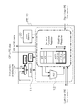
- FIG. 10 is a diagram showing a configuration of one PE 110 in a PE array included in a conventional SIMD processor.
- the PE 110 stores an instruction buffer (instb) 111 for storing instructions issued from the CP 130 (FIG. 9), general purpose registers (General Purpose Registers) r0 to r7, and arithmetic units (ALU: Arithmetic Logic Unit). ) 112, and an entry / exit to the connection network between PEs (Left / Right Inter PE Connection), and a local memory 120 for each PE (Local Memory). All the PEs 110 simultaneously execute a single instruction issued from the CP 130 every cycle.
- instruction buffer instb
- general purpose registers General Purpose Registers
- ALU Arithmetic Logic Unit
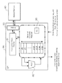
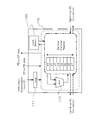
- FIG. 1 shows a configuration of 1 PE 10 in a PE array included in a SIMD processor according to this embodiment.
- the PE 10 includes an instruction buffer (instb) 11, general purpose registers (General Purpose Registers) r 0 to r 15, an arithmetic unit (ALU: Arithmetic Logic Unit) 12, and an entrance / exit to a connection network between PEs (Left / Right Interchange). PE Connection) and local memory 20 for each PE.
- the PE 10 further includes registers stop and mode and a selector sel.
- FIG. 1 components (thick line portions) added to FIG. 10, that is, registers stop, mode, selector sel, registers cm, sx, and sy will be described.
- the register stop is a control register for keeping the operation of the PE 10 stopped during the instruction / data distribution operation.
- the register mode is a 1-bit operation mode selection register for switching between a systolic operation and a conventional SIMD operation.
- the selector sel is a selector that selects whether or not an instruction issued from the CP is stored in the instruction buffer (instb) 11.
- the registers cm, sx, and sy are a general-purpose register (waiting register) group having a data waiting function in which a predetermined counter register is decremented each time a write to the register occurs during a systolic operation.
- FIG. 2 is a diagram schematically showing the configuration of the control processor (CP) 30 included in the SIMD processor according to the present embodiment.
- CP 30 has a data path for performing its own operation, and is an instruction / data cache (Instruction / Data Cache) 31, and a memory access adjustment unit, like CP 130 in the conventional SIMD processor. It is connected to a global memory 40 via an arbiter 33.
- the CP 30 reads and issues commands to be executed in its own data path and commands to be broadcast to the entire PE array from the global memory 40, and is transmitted and received between the calculation data on the CP 30 and the local memory 20 of the PE 10. Data to be read from the global memory 40 or written to the global memory 40.
- FIG. 3 is a diagram illustrating an example of an instruction format in the SIMD processor according to the present embodiment.
- the CP 30 in the SIMD processor of the present embodiment is different from the CP 130 in the conventional SIMD processor, and sends instructions and / or data to a specific PE at the same time and executes them to a specific PE or a plurality of designated PEs.
- An instruction set having an instruction format as shown in FIG. 3 is used.
- the instruction format of CP30 has a different format according to the bit pattern of the header section of the instruction.
- the bit pattern of the “header” part is “10”, it indicates that the instruction A is to be distributed to the specific PE 10, and as a subsequent instruction, an instruction B whose bit pattern of the header part is always “11”
- the instruction A is written to the instruction buffer (instb) 11 of the PE of the PE number indicated by the “Target PEID” part of the instruction B, and the PE register of the PE number indicated by the “Target reg ID” part of the instruction B is written. Specifies the operation of writing the “data” part of the instruction B.
- the value of the “data” part is stored in the register of the number indicated by the “Target reg ID” part of the PE of the PE number indicated by the “Target PEID” part of the instruction.
- the instruction stored in the instruction buffer (instb) 11 writes the value of the data part to the register cm of the PE 10 having cm as the source operand. specify.
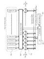
- FIG. 4 shows the overall configuration of the PE array in the SIMD processor according to this embodiment.
- the bold line portion indicates a global access arbitration unit (Global Access Arbiter) 50, which is a circuit element newly added in the present invention, in addition to the individual PEs 10, with respect to the conventional SIMD processor.
- Global Access Arbiter Global Access Arbiter
- the global access arbitration unit 50 is a module that manages the local memory blocks of all the PEs 20 so that they can be used together as a multi-bank cache memory body, and memory access is simultaneously generated from a large number of PEs 10 during the systolic operation mode. If this occurs, the memory access is arbitrated.
- the following method can be considered. In other words, when there are memory access requests from two or more PEs simultaneously, the operation of the entire PE array is temporarily stopped, the memory access requests of each PE are answered one by one, and then the operation of the PE array is resumed.
- An implementation method with low performance but low hardware implementation cost is conceivable.
- a mounting method that has the highest performance but high hardware implementation cost is conceivable, in which local memory blocks of all PEs are connected by a crossbar mechanism to respond to a large number of memory access requests with the shortest possible delay. Any mounting method may be adopted as long as the maximum memory access delay can be determined statically when arbitrary program code is executed in a superimposed manner.
- the CP 30 simultaneously reads two instructions, the instruction at the address indicated by the value of the program counter (PC: Program Counter) 35 and the instruction at the next address. However, whether the count value of the PC 35 is incremented or decremented every cycle and how the read instruction is processed is determined by “header” of the read first instruction A. It is determined as follows according to the value of the part.
- PC Program Counter
- an instruction having a “header” value of “10” includes a “counter” portion. It is assumed that a value equal to or greater than the number of “waiting registers” among the source operands of the instruction is set in the “counter” portion.
- the PE number specified by the “target PEID” portion of the instruction A is on the PE.
- a write operation P is performed on the register sx.
- the value “1” is set in the “counter” portion of the instruction C in the instruction buffer (instb) 11 of the PE, and the register sx is the only “waiting register” in the source operand of the instruction C.
- the “counter” part of the instruction C includes The value 1 is set again.
- the “counter” portion is not 1 but 0 which is the decrement result. Since it is set, the instruction C is continuously executed on the PE.
- CP30 executes an instruction A in which the waiting register cm is specified in the “Target reg ID” part in the systolic operation, all having cm as a source operand in the instruction buffer (instb) 11
- the writing operation P to cm occurs with respect to the PE.
- the value “2” is set in the “counter” part of the instruction C in the instruction buffer (instb) 11 of the PE, and cm and sy are both source operands of the instruction C
- the PE does not start executing the instruction C only by the write operation P to cm caused by the execution of the instruction A. However, the PE does not start the execution of the instruction C.
- the write operation Q occurs, the PE starts executing the instruction C.
- the value 2 is copied from the “header” part of the instruction C and set again in the “counter” part of the instruction C.
- a write operation occurs simultaneously with respect to the queuing registers sx and cm of the PE, 0, which is the result of decrementing this twice only, is set in the “counter” section again. Therefore, the instruction C is continuously executed on the PE.
- the CP 30 can instruct the PE to execute the instruction stored in the instruction buffer (instb) 11 by issuing the “systolic operation” instruction instruction. If the instruction stored in the instruction buffer (instb) 11 designates the “waiting register” of another PE as the write destination of the execution result, the execution of the instruction propagates between the PEs. . Further, since the CP 30 can perform a write operation on the registers cm of a large number of PEs, it is possible to simultaneously shift a large number of PEs from the “waiting” state to the “execution” state. In this manner, the CP 30 can cause a systolic instruction execution chain on the PE array by issuing a “systolic operation” instruction.
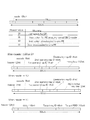
- FIG. 5A shows pseudo code corresponding to the loop portion of the process of mapping to the PE array in this embodiment.
- the pseudo code reads the data from the array A, adds the variable a, and writes it to the array B, for a total of 8 iterations for elements 0 to 7 of the array A. This is the program code to be executed in the configuration.
- FIG. 5B shows a case where the processing of FIG. 5A is mapped to PEs PE0, PE1, PE2, PE4 and PE10 in the PE array group of the SIMD processor of this embodiment. Indicates the instruction to be performed.
- add shown in FIG. 5B means an addition instruction, and has two source register number designations (A and cm) and one destination register number designation (1sx).
- a single alphabet (A, B, a) represents a constant (A is the absolute address of array A in this case).
- the instruction buffer (instb) 11 When executing the instruction stored in the instruction buffer (instb) 11, if a constant is specified as an operand, it is assumed that the constant is stored in the register of register number 0 (ie, r0), and the register r0 Operates to read a value.
- the destination register number is specified by a combination of a PE number and a register name. For example, if it is 1 sx, the operation is performed so that the operation result is stored in the sx register of the PE with PE number 1.
- CP30 in order for CP30 to store the instruction “add A, cm, 1sx” in the instruction buffer (instb) 11 of PE0, the “header” part is set to 10, and the “opcode” part is set.
- a bit string representing an add instruction “1st operating reg ID” is 0, “2nd operating reg ID” is 0xd, “Destination reg ID” is 0xe, and (the PE number of the operation result storage destination is 1) “PEID part ”,“ Counter ”part is 1 instruction,“ header ”part is 11,“ data ”part is absolute address of array A,“ Target reg ID ”part is 0, (add Since the PE number of the owner of the instruction storage instb is 0) "Target. EID "the prepared instructions and which is set to 0, it is sufficient to run the CP30.
- gld and gst shown in FIG. 5B are a load instruction and a store instruction for the global memory, respectively.
- the load instruction has the load target address as the first source operand without having the second source operand, and has the designation of the destination register number of the storage destination of the loaded data.
- the store instruction has a store target address as the first source operand, a register number storing the write data as the second source operand, and does not have a destination register number designation (indicated as NULL in FIG. 5B).
- 1sx, 2sx, 4sx, 4sy, and NULL in the destination field designation of each instruction are sx of PE1, sx of PE2, sx of PE4, Indicates sy and no destination.
- FIG. 5 (c) shows, as an example, a time chart of the operation from when the instruction code of FIG. 5 (b) is distributed to the PE array by the CP 30 until the operation ends.
- the vertical axis represents time (unit: cycle)
- the horizontal axis represents the operation of the CP 30 and the operation on the PE side.
- the operation on the PE side is displayed separately for each iteration.
- the operation status of the CP 30 and PE in each cycle is shown.
- INSTB_BC (PE0) written at the top of the column indicating the operation of CP30 reads an instruction whose “header” portion is “10” (and an instruction whose subsequent “header” portion is “11”). Indicates that the operation of distributing to PE0 has occurred in the cycle.
- GO (1, cm) means that an instruction whose “header” part is “11” and whose value of the “data” part is “1” is read out of PE0, PE1, PE2, PE4, and PE10. This indicates that an operation in which the instruction in the instruction buffer (instb) 11 writes 1 as the value of the “data” part of the instruction to the register cm of the PE including the register cm as a source operand has occurred in the cycle.
- the CLD and CST perform load operation and store operation via the cache memory or the like to the global memory generated as a result of the arbitration by the global access arbitration unit 50 due to the issuing of the gld and gst instructions on the PE side, respectively.
- PEx represents a cycle in which a PE with a PE number x executes an instruction.
- PEx / y indicates that PEx and PEy executed an instruction in the same cycle.
- * or + is added to the end of PEx that executed the gld or gst instruction.
- a dotted arrow indicates a flow from when the gld instruction is executed on PE1 until load data is sent to PE2.
- a black rectangle in FIG. 5C represents a load data waiting cycle, and “-” represents a transfer cycle between PEs.
- the filled black circle indicates that the instruction is executed on the corresponding PE (horizontal axis).
- An arrow PEx ⁇ PEy indicates that data transfer has occurred between PEx and PEy.
- the load access delay for the global memory 40 is three cycles. Therefore, the arrow from PE1 to PE2 extends over 3 cycles.
- no crossing occurs between a plurality of arrows in the same direction. This indicates that there is no collision regarding data transfer using the coupling line between PEs over a total of 21 cycles in which the PE array performs systolic operation.
- the arrow in the left ⁇ right (or left ⁇ right) direction from PEx to PEy in cycle P indicates the connection between adjacent PEs in the direction of PEx ⁇ PEy (or PEx ⁇ PEy) in the cycle. Indicates that data transfer is performed using a line.
- the brightness of the arrows and filled circles is changed in order to make it easy to distinguish between individual iterations.
- FIGS. 5C and 6 show diagrams assuming that the delay of the load access by the PE for the global memory is 3 cycles.
- the delay is smaller than 3, for example, 2, the instruction assigned to PE10 may be assigned to PE9 as shown in FIG.
- the load access delay is larger than 3, for example, 4, for example, the instruction assigned to PE10 may be assigned to PE11 as shown in FIG. 7B.
- FIG. 8 shows pseudo code when the program code of FIG. 5A is sequentially executed on the CP 30.
- CADD represents an add instruction.
- CLD and CST represent a memory load instruction and a memory store instruction, respectively. These are all instructions whose “header” part is 00.
- the performance improvement is small when the number of iterations is small. However, if the number of iterations is 1000, the 5 cycles required to distribute the instructions to the PE array can be ignored. Further, in this embodiment, it can be executed with a throughput of one cycle for each iteration. On the other hand, referring to FIG. 7, when the same processing is executed on the CP 30, it takes 6 cycles for each iteration. Therefore, the SIMD processor of the present invention provides a performance improvement of about 6 times.
Abstract
L'invention porte sur un processeur à instruction unique, données multiples (SIMD) qui permet à un programme d'être traité à grande vitesse à l'aide d'éléments de traitement du processeur SIMD sans modifier l'agencement de données dans une mémoire globale. Le processeur SIMD comprend un processeur de commande (CP) et une pluralité d'éléments de traitement (PE), la pluralité de PE réalisant une opération SIMD pour exécuter une instruction unique délivrée par le CP, un PE spécifique parmi la pluralité de PE réalisant une opération de distribution d'instruction/données pour recevoir l'instruction et des données délivrées par le CP, et pour l'instruction qui a été diffusée à chaque PE par le CP dans l'opération de distribution d'instruction/données, chacun des PE réalise une opération systolique pour l'exécution après que des opérandes sources de l'instruction ont été collectées.
Priority Applications (1)
| Application Number | Priority Date | Filing Date | Title |
|---|---|---|---|
| JP2012501811A JP5708634B2 (ja) | 2010-02-24 | 2011-02-23 | Simdプロセッサ |
Applications Claiming Priority (2)
| Application Number | Priority Date | Filing Date | Title |
|---|---|---|---|
| JP2010-038976 | 2010-02-24 | ||
| JP2010038976 | 2010-02-24 |
Publications (1)
| Publication Number | Publication Date |
|---|---|
| WO2011105408A1 true WO2011105408A1 (fr) | 2011-09-01 |
Family
ID=44506813
Family Applications (1)
| Application Number | Title | Priority Date | Filing Date |
|---|---|---|---|
| PCT/JP2011/053935 WO2011105408A1 (fr) | 2010-02-24 | 2011-02-23 | Processeur simd |
Country Status (2)
| Country | Link |
|---|---|
| JP (1) | JP5708634B2 (fr) |
| WO (1) | WO2011105408A1 (fr) |
Cited By (1)
| Publication number | Priority date | Publication date | Assignee | Title |
|---|---|---|---|---|
| JP2021157771A (ja) * | 2018-10-18 | 2021-10-07 | シャンハイ カンブリコン インフォメーション テクノロジー カンパニー リミテッドShanghai Cambricon Information Technology Co., Ltd. | ネットワークオンチップによるデータ処理方法及び装置 |
Citations (6)
| Publication number | Priority date | Publication date | Assignee | Title |
|---|---|---|---|---|
| JPS63501530A (ja) * | 1985-09-17 | 1988-06-09 | ザ・ジョンズ・ホプキンス・ユニバ−シティ | メモリをリンクしたウエ−ブフロント・アレイ・プロセッサ |
| US4967340A (en) * | 1985-06-12 | 1990-10-30 | E-Systems, Inc. | Adaptive processing system having an array of individually configurable processing components |
| JPH0635878A (ja) * | 1992-05-22 | 1994-02-10 | Internatl Business Mach Corp <Ibm> | 単一命令複数データ/複数命令複数データ・プロセッサ・アレイ用コントローラ |
| US5659780A (en) * | 1994-02-24 | 1997-08-19 | Wu; Chen-Mie | Pipelined SIMD-systolic array processor and methods thereof |
| JP2002175283A (ja) * | 2000-12-05 | 2002-06-21 | Matsushita Electric Ind Co Ltd | シストリックアレイ型演算器 |
| JP2008034953A (ja) * | 2006-07-26 | 2008-02-14 | Kobe Univ | 画像処理プロセッサ |
Family Cites Families (7)
| Publication number | Priority date | Publication date | Assignee | Title |
|---|---|---|---|---|
| EP0266300B1 (fr) * | 1986-10-29 | 1994-12-07 | United Technologies Corporation | Architecture de multiprocesseur modulaire en réseau à N dimensions |
| JPH0668053A (ja) * | 1992-08-20 | 1994-03-11 | Toshiba Corp | 並列計算機 |
| CA2129882A1 (fr) * | 1993-08-12 | 1995-02-13 | Soheil Shams | Reseau de communication entre multiprocesseurs simd dynamiquement reconfigurable et appareil utilisant ce reseau |
| JP2657903B2 (ja) * | 1994-11-29 | 1997-09-30 | 乾彌 呉 | パイプライン式及び心収縮式の単命令多重データストリームのアレイプロセッサ及びその方法 |
| US5680597A (en) * | 1995-01-26 | 1997-10-21 | International Business Machines Corporation | System with flexible local control for modifying same instruction partially in different processor of a SIMD computer system to execute dissimilar sequences of instructions |
| JP3987784B2 (ja) * | 2002-10-30 | 2007-10-10 | Necエレクトロニクス株式会社 | アレイ型プロセッサ |
| JP4477959B2 (ja) * | 2004-07-26 | 2010-06-09 | 独立行政法人理化学研究所 | ブロードキャスト型並列処理のための演算処理装置 |
-
2011
- 2011-02-23 JP JP2012501811A patent/JP5708634B2/ja active Active
- 2011-02-23 WO PCT/JP2011/053935 patent/WO2011105408A1/fr active Application Filing
Patent Citations (6)
| Publication number | Priority date | Publication date | Assignee | Title |
|---|---|---|---|---|
| US4967340A (en) * | 1985-06-12 | 1990-10-30 | E-Systems, Inc. | Adaptive processing system having an array of individually configurable processing components |
| JPS63501530A (ja) * | 1985-09-17 | 1988-06-09 | ザ・ジョンズ・ホプキンス・ユニバ−シティ | メモリをリンクしたウエ−ブフロント・アレイ・プロセッサ |
| JPH0635878A (ja) * | 1992-05-22 | 1994-02-10 | Internatl Business Mach Corp <Ibm> | 単一命令複数データ/複数命令複数データ・プロセッサ・アレイ用コントローラ |
| US5659780A (en) * | 1994-02-24 | 1997-08-19 | Wu; Chen-Mie | Pipelined SIMD-systolic array processor and methods thereof |
| JP2002175283A (ja) * | 2000-12-05 | 2002-06-21 | Matsushita Electric Ind Co Ltd | シストリックアレイ型演算器 |
| JP2008034953A (ja) * | 2006-07-26 | 2008-02-14 | Kobe Univ | 画像処理プロセッサ |
Cited By (4)
| Publication number | Priority date | Publication date | Assignee | Title |
|---|---|---|---|---|
| JP2021157771A (ja) * | 2018-10-18 | 2021-10-07 | シャンハイ カンブリコン インフォメーション テクノロジー カンパニー リミテッドShanghai Cambricon Information Technology Co., Ltd. | ネットワークオンチップによるデータ処理方法及び装置 |
| JP2021166034A (ja) * | 2018-10-18 | 2021-10-14 | シャンハイ カンブリコン インフォメーション テクノロジー カンパニー リミテッドShanghai Cambricon Information Technology Co., Ltd. | ネットワークオンチップによるデータ処理方法及び装置 |
| JP7074832B2 (ja) | 2018-10-18 | 2022-05-24 | シャンハイ カンブリコン インフォメーション テクノロジー カンパニー リミテッド | ネットワークオンチップによるデータ処理方法及び装置 |
| JP7074833B2 (ja) | 2018-10-18 | 2022-05-24 | シャンハイ カンブリコン インフォメーション テクノロジー カンパニー リミテッド | ネットワークオンチップによるデータ処理方法及び装置 |
Also Published As
| Publication number | Publication date |
|---|---|
| JP5708634B2 (ja) | 2015-04-30 |
| JPWO2011105408A1 (ja) | 2013-06-20 |
Similar Documents
| Publication | Publication Date | Title |
|---|---|---|
| RU2427895C2 (ru) | Оптимизированная для потоков многопроцессорная архитектура | |
| US7159099B2 (en) | Streaming vector processor with reconfigurable interconnection switch | |
| US8412917B2 (en) | Data exchange and communication between execution units in a parallel processor | |
| JP4156794B2 (ja) | iVLIWのPE間通信を用いた効率的な同期MIMD動作のための方法および装置 | |
| US9158575B2 (en) | Multithreaded processor array with heterogeneous function blocks communicating tokens via self-routing switch fabrics | |
| US11550750B2 (en) | Memory network processor | |
| EP1333381A2 (fr) | Système et procédé pour traiter des images et compilateur utilisable dans ce système | |
| US8892620B2 (en) | Computer for Amdahl-compliant algorithms like matrix inversion | |
| JP2014501009A (ja) | データを移動させるための方法及び装置 | |
| KR102090885B1 (ko) | 배선 복잡성이 감소된 시프트 레지스터 | |
| JP4624098B2 (ja) | プロセッサのアドレス発生ユニット | |
| JP2011523132A (ja) | 実行エンジン | |
| US8024549B2 (en) | Two-dimensional processor array of processing elements | |
| US8190856B2 (en) | Data transfer network and control apparatus for a system with an array of processing elements each either self- or common controlled | |
| US8060726B2 (en) | SIMD microprocessor, image processing apparatus including same, and image processing method used therein | |
| US11782760B2 (en) | Time-multiplexed use of reconfigurable hardware | |
| JP5708634B2 (ja) | Simdプロセッサ | |
| KR100267092B1 (ko) | 멀티미디어신호프로세서의단일명령다중데이터처리 | |
| JP5370352B2 (ja) | Simd型プロセッサアレイシステム及びそのデータ転送方法 | |
| JP5358315B2 (ja) | 並列計算装置 | |
| JP2024505440A (ja) | トリガ条件に依存する命令実行のための回路及び方法 | |
| Frijns et al. | Dc-simd: Dynamic communication for simd processors | |
| CN117009287A (zh) | 一种于弹性队列存储的动态可重构处理器 | |
| Ito et al. | Reconfigurable instruction-level parallel processor architecture | |
| JP2006196015A (ja) | データ処理プロセッサおよびシステム |
Legal Events
| Date | Code | Title | Description |
|---|---|---|---|
| 121 | Ep: the epo has been informed by wipo that ep was designated in this application |
Ref document number: 11747368 Country of ref document: EP Kind code of ref document: A1 |
|
| WWE | Wipo information: entry into national phase |
Ref document number: 2012501811 Country of ref document: JP |
|
| NENP | Non-entry into the national phase |
Ref country code: DE |
|
| 122 | Ep: pct application non-entry in european phase |
Ref document number: 11747368 Country of ref document: EP Kind code of ref document: A1 |