WO2011104946A1 - 液晶パネルの駆動方法と液晶表示装置 - Google Patents
液晶パネルの駆動方法と液晶表示装置 Download PDFInfo
- Publication number
- WO2011104946A1 WO2011104946A1 PCT/JP2010/069852 JP2010069852W WO2011104946A1 WO 2011104946 A1 WO2011104946 A1 WO 2011104946A1 JP 2010069852 W JP2010069852 W JP 2010069852W WO 2011104946 A1 WO2011104946 A1 WO 2011104946A1
- Authority
- WO
- WIPO (PCT)
- Prior art keywords
- common electrode
- liquid crystal
- voltage
- electrode voltage
- display device
- Prior art date
- Legal status (The legal status is an assumption and is not a legal conclusion. Google has not performed a legal analysis and makes no representation as to the accuracy of the status listed.)
- Ceased
Links
Images








Classifications
-
- G—PHYSICS
- G09—EDUCATION; CRYPTOGRAPHY; DISPLAY; ADVERTISING; SEALS
- G09G—ARRANGEMENTS OR CIRCUITS FOR CONTROL OF INDICATING DEVICES USING STATIC MEANS TO PRESENT VARIABLE INFORMATION
- G09G3/00—Control arrangements or circuits, of interest only in connection with visual indicators other than cathode-ray tubes
- G09G3/20—Control arrangements or circuits, of interest only in connection with visual indicators other than cathode-ray tubes for presentation of an assembly of a number of characters, e.g. a page, by composing the assembly by combination of individual elements arranged in a matrix no fixed position being assigned to or needed to be assigned to the individual characters or partial characters
- G09G3/34—Control arrangements or circuits, of interest only in connection with visual indicators other than cathode-ray tubes for presentation of an assembly of a number of characters, e.g. a page, by composing the assembly by combination of individual elements arranged in a matrix no fixed position being assigned to or needed to be assigned to the individual characters or partial characters by control of light from an independent source
- G09G3/36—Control arrangements or circuits, of interest only in connection with visual indicators other than cathode-ray tubes for presentation of an assembly of a number of characters, e.g. a page, by composing the assembly by combination of individual elements arranged in a matrix no fixed position being assigned to or needed to be assigned to the individual characters or partial characters by control of light from an independent source using liquid crystals
- G09G3/3611—Control of matrices with row and column drivers
- G09G3/3648—Control of matrices with row and column drivers using an active matrix
- G09G3/3655—Details of drivers for counter electrodes, e.g. common electrodes for pixel capacitors or supplementary storage capacitors
-
- G—PHYSICS
- G02—OPTICS
- G02F—OPTICAL DEVICES OR ARRANGEMENTS FOR THE CONTROL OF LIGHT BY MODIFICATION OF THE OPTICAL PROPERTIES OF THE MEDIA OF THE ELEMENTS INVOLVED THEREIN; NON-LINEAR OPTICS; FREQUENCY-CHANGING OF LIGHT; OPTICAL LOGIC ELEMENTS; OPTICAL ANALOGUE/DIGITAL CONVERTERS
- G02F1/00—Devices or arrangements for the control of the intensity, colour, phase, polarisation or direction of light arriving from an independent light source, e.g. switching, gating or modulating; Non-linear optics
- G02F1/01—Devices or arrangements for the control of the intensity, colour, phase, polarisation or direction of light arriving from an independent light source, e.g. switching, gating or modulating; Non-linear optics for the control of the intensity, phase, polarisation or colour
- G02F1/13—Devices or arrangements for the control of the intensity, colour, phase, polarisation or direction of light arriving from an independent light source, e.g. switching, gating or modulating; Non-linear optics for the control of the intensity, phase, polarisation or colour based on liquid crystals, e.g. single liquid crystal display cells
- G02F1/133—Constructional arrangements; Operation of liquid crystal cells; Circuit arrangements
- G02F1/1333—Constructional arrangements; Manufacturing methods
- G02F1/1343—Electrodes
- G02F1/134309—Electrodes characterised by their geometrical arrangement
- G02F1/134318—Electrodes characterised by their geometrical arrangement having a patterned common electrode
-
- G—PHYSICS
- G09—EDUCATION; CRYPTOGRAPHY; DISPLAY; ADVERTISING; SEALS
- G09G—ARRANGEMENTS OR CIRCUITS FOR CONTROL OF INDICATING DEVICES USING STATIC MEANS TO PRESENT VARIABLE INFORMATION
- G09G2320/00—Control of display operating conditions
- G09G2320/02—Improving the quality of display appearance
- G09G2320/028—Improving the quality of display appearance by changing the viewing angle properties, e.g. widening the viewing angle, adapting the viewing angle to the view direction
-
- G—PHYSICS
- G09—EDUCATION; CRYPTOGRAPHY; DISPLAY; ADVERTISING; SEALS
- G09G—ARRANGEMENTS OR CIRCUITS FOR CONTROL OF INDICATING DEVICES USING STATIC MEANS TO PRESENT VARIABLE INFORMATION
- G09G3/00—Control arrangements or circuits, of interest only in connection with visual indicators other than cathode-ray tubes
- G09G3/20—Control arrangements or circuits, of interest only in connection with visual indicators other than cathode-ray tubes for presentation of an assembly of a number of characters, e.g. a page, by composing the assembly by combination of individual elements arranged in a matrix no fixed position being assigned to or needed to be assigned to the individual characters or partial characters
- G09G3/34—Control arrangements or circuits, of interest only in connection with visual indicators other than cathode-ray tubes for presentation of an assembly of a number of characters, e.g. a page, by composing the assembly by combination of individual elements arranged in a matrix no fixed position being assigned to or needed to be assigned to the individual characters or partial characters by control of light from an independent source
- G09G3/36—Control arrangements or circuits, of interest only in connection with visual indicators other than cathode-ray tubes for presentation of an assembly of a number of characters, e.g. a page, by composing the assembly by combination of individual elements arranged in a matrix no fixed position being assigned to or needed to be assigned to the individual characters or partial characters by control of light from an independent source using liquid crystals
- G09G3/3611—Control of matrices with row and column drivers
- G09G3/3614—Control of polarity reversal in general
Definitions
- the present invention relates to a driving method of a liquid crystal panel that performs AC driving and a liquid crystal display device using the driving method.
- a data signal voltage level output from the source driver and applied to the pixel electrode and a common electrode voltage level output from the common electrode signal generation circuit and applied to the common electrode are set for a certain period.
- AC driving that is reversed every time is performed.
- an inrush current to the liquid crystal capacitance occurs at the timing of polarity inversion.
- Patent Document 1 describes a configuration in which a single liquid crystal panel is driven by a plurality of sets of source drivers and gate drivers.
- the alternating timing of each drive voltage applied to each group of the liquid crystal panel is applied to all pixels by making each group different.
- the inrush current (rush current) flowing through the liquid crystal panel capacitance is reduced.
- the inventors of the present application pay attention to the point that an inrush current flows in the COM signal line when the COM signal is inverted (when the COM voltage polarity is inverted), and by improving the inversion mechanism of the COM signal, the inrush current is further improved. It has been found that it can be further reduced.
- the present invention has been made in view of the above problems, and an object of the present invention is to provide a liquid crystal display device in which the current value of an instantaneous inrush current when the polarity of a COM signal (COM voltage) is reversed is reduced. It is in.
- the liquid crystal display device includes: An active matrix in which a plurality of data signal lines and a plurality of scanning signal lines intersecting the data signal lines are formed, and an active element and a pixel electrode are arranged at each intersection of the data signal line and the scanning signal line A substrate, A counter substrate disposed opposite to the active matrix substrate; A plurality of common electrodes disposed on the active matrix substrate or the counter substrate; A liquid crystal layer disposed between the active matrix substrate and the counter substrate; Each of the plurality of pixel electrodes includes a region facing the first common electrode of the plurality of common electrodes, and a second of the plurality of common electrodes different from the first common electrode.
- a liquid crystal display device in which a region facing the common electrode is formed, First common electrode voltage applying means for applying a first common electrode voltage to the first common electrode; A second common electrode voltage applying means for applying a second common electrode voltage having a voltage value different from the first common electrode voltage to the second common electrode; Control means for controlling the application of the common electrode applied voltage to each common electrode by the first common electrode voltage applying means and the second common electrode voltage applying means and inverting the polarity of each common electrode voltage every certain period And When each common electrode voltage starts to rise from a certain voltage to a predetermined voltage higher than the certain voltage due to polarity reversal, at the rising edge of polarity reversal, each common electrode voltage changes from a certain voltage to a certain voltage due to polarity reversal.
- the control means includes (1) Between a rising edge of the polarity reversal of the first common electrode voltage and a rising edge of the polarity reversal of the second common electrode voltage in a certain period; and (2) Between the fall of the polarity reversal of the first common electrode voltage and the fall of the polarity reversal of the second common electrode voltage in the certain period, It is characterized by being configured to control so as to provide a time difference in at least one of the above.
- the liquid crystal display device can provide a liquid crystal display device in which the current value of the instantaneous inrush current when the polarity of the COM signal (COM voltage) is reversed is reduced.
- COM signal COM voltage
- a description will be given by taking as an example a case where a common electrode is disposed on the counter substrate.
- each of the plurality of pixel electrodes has a region facing the first common electrode among the plurality of common electrodes with the liquid crystal layer interposed therebetween, and a plurality of the plurality of pixel electrodes with the liquid crystal layer interposed therebetween.
- the common electrode is formed with a region facing the second common electrode different from the first common electrode, and the first common electrode and the second common electrode are different from each other.
- a common electrode voltage is applied.
- each pixel electrode includes at least a first region facing the first common electrode with the liquid crystal layer interposed therebetween, and a second region facing the second common electrode with the liquid crystal layer interposed therebetween. Will have.
- the first common electrode voltage is applied to the first common electrode
- the second common electrode voltage is applied to the second common electrode.
- the liquid crystal layer in the first region that is, the first region of the pixel electrode and the first common electrode voltage are different from each other.
- the liquid crystal layer sandwiched between the common electrode and the liquid crystal layer in the second region that is, the liquid crystal layer sandwiched between the second region of the pixel electrode and the second common electrode. The voltage can be made different.
- the display screen of the liquid crystal display device is inclined in the middle direction.
- the display quality when viewed from above can be improved. That is, the viewing angle characteristics of the liquid crystal display device can be improved.
- the amplitude of either the first common electrode voltage (COM1) applied to the first common electrode or the second common electrode voltage (COM2) applied to the second common electrode is set to the common electrode voltage (although it has the effect of widening the viewing angle by expanding it from the amplitude of (COM), there arises a problem that the inrush current generated when the COM signal is inverted increases.
- the configuration (1) having COM1 and COM2 as compared with the configuration (1) in which the COM amplitude is 5 Vpp the COM1 amplitude is 4 Vpp and the COM2 amplitude is 8.5 Vpp.
- the timing of the polarity inversion of the first common electrode voltage at least one of the rising edge of the polarity inversion of each common electrode voltage and the falling edge of the polarity inversion in a certain horizontal scanning period.
- liquid crystal display device having a wide viewing angle characteristic that achieves low power consumption by suppressing the occurrence of inconvenient inrush current at a low cost.
- the configuration of the present invention a wide viewing angle characteristic is realized and the instantaneous inrush current value (peak value) at the time of polarity reversal of the common electrode voltage, which has been a problem in the conventional configuration, can be reduced. Can do.
- the polarity is an expression relatively indicating the relationship between the common electrode potential and the source potential during the period in which the voltage is applied to the pixel electrode, and the source potential level is relatively higher than the common electrode potential.
- the state is called positive polarity, and the state where the source potential level is relatively low with respect to the common electrode potential is called negative polarity.
- the liquid crystal display device is An active matrix in which a plurality of data signal lines and a plurality of scanning signal lines intersecting the data signal lines are formed, and an active element and a pixel electrode are arranged at each intersection of the data signal line and the scanning signal line A substrate, A counter substrate disposed opposite to the active matrix substrate; A plurality of common electrodes disposed on the active matrix substrate or the counter substrate; A liquid crystal layer disposed between the active matrix substrate and the counter substrate; Each of the plurality of pixel electrodes includes a region facing the first common electrode of the plurality of common electrodes, and a second of the plurality of common electrodes different from the first common electrode.
- a liquid crystal display device in which a region facing the common electrode is formed, First common electrode voltage applying means for applying a first common electrode voltage to the first common electrode; A second common electrode voltage applying means for applying a second common electrode voltage having a voltage value different from the first common electrode voltage to the second common electrode; Control means for controlling the application of the common electrode applied voltage to each common electrode by the first common electrode voltage applying means and the second common electrode voltage applying means and inverting the polarity of each common electrode voltage every certain period And When each common electrode voltage starts to rise from a certain voltage to a predetermined voltage higher than the certain voltage due to polarity reversal, at the rising edge of polarity reversal, each common electrode voltage changes from a certain voltage to a certain voltage due to polarity reversal.
- the control means includes (1) Between a rising edge of the polarity reversal of the first common electrode voltage and a rising edge of the polarity reversal of the second common electrode voltage in a certain period; and (2) Between the fall of the polarity reversal of the first common electrode voltage and the fall of the polarity reversal of the second common electrode voltage in the certain period, It is characterized by being configured to control so as to provide a time difference in at least one of the above.
- each of the pixel electrodes has a region facing the first common electrode of the plurality of common electrodes with the liquid crystal layer interposed therebetween, and a region of the plurality of common electrodes with the liquid crystal layer interposed therebetween.
- the current value (peak value) of the instantaneous inrush current when the polarity of the common electrode voltage is reversed It is possible to provide a liquid crystal display device in which the above is reduced.
- FIG. 1 is a block diagram of a liquid crystal display device according to an embodiment of the present invention. It is sectional drawing of the board
- FIG. 2 is a plan view of a part of the display panel of the liquid crystal display device shown in FIG. 1.
- FIG. 2 is a plan view of a common electrode forming surface side of a counter substrate provided in the display panel of the liquid crystal display device illustrated in FIG. 1. It is a timing chart ((a) in the figure) of a signal in each of the first common electrode and the second common electrode, and a current waveform diagram ((b) in the figure) along the timing chart.
- FIG. 2 is a timing chart showing a circuit configuration shown by using a part of FIG. 1 and its effect.
- 10 is a timing chart of signals in each of the first common electrode and the second common electrode of the counter substrate provided in the display panel of the liquid crystal display device, according to still another embodiment of the liquid crystal display device according to the present invention.
- 10 is a timing chart of signals in each of the first common electrode and the second common electrode of the counter substrate provided in the display panel of the liquid crystal display device, according to still another embodiment of the liquid crystal display device according to the present invention.
- FIG. 1 is a schematic block diagram showing the overall configuration of an active matrix liquid crystal display device according to the present embodiment.
- the liquid crystal display device 1 includes a display panel including a pixel array ARY, a scanning signal line driving circuit GD, and a data signal line driving circuit SD, and a control device (control means) including a timing controller CTRL. And an external power supply circuit VGEN.
- pixels PIX are arranged in a matrix in the vicinity of the intersection positions of a large number of scanning signal lines GL and a large number of data signal lines SL that intersect each other. Each pixel PIX is connected to an adjacent scanning signal line GL and data signal line SL.
- the pixel array ARY, the data signal line driving circuit SD, and the scanning signal line driving circuit GD are formed on the same substrate. These are the video signal dat, the clock signal cks, the start signal from the timing controller CTRL. It is driven according to sps, clock signal ckg, start signal spg, pulse width control signal gps, and various drive power sources from the external power supply circuit VGEN.
- the data signal line driving circuit SD samples the input video signal dat in synchronization with a timing signal such as the clock signal cks, amplifies it as necessary, and writes it to each data signal line SL.
- the scanning signal line driving circuit GD sequentially selects the scanning signal lines GL in synchronization with timing signals such as the clock signal ckg, and controls the switching elements in the pixels PIX to open / close the data signal lines SL.
- the written video signal (data) dat is written to the corresponding pixel PIX and the data written to each pixel PIX is held.
- one color is represented by three pixels PIX of R, G, and B.
- FIG. 2 is a cross-sectional view of the substrate structure constituting the pixel array ARY.
- the display panel of the liquid crystal display device 1 includes an active matrix substrate 20 having a pixel electrode 24 and an alignment film 26 provided on an insulating substrate 22, and a counter electrode having a common electrode 44 and an alignment film 46 provided on an insulating substrate 42.
- a substrate 40 and a liquid crystal layer 60 provided between the active matrix substrate 20 and the counter substrate 40 are provided.
- the active matrix substrate 20 and the counter substrate 40 are provided with polarizing plates (not shown), and the polarizing axes of the polarizing plates have a crossed Nicols relationship.
- the thickness of the liquid crystal layer 60 is substantially constant.
- the above-described pixel PIX (FIG. 1) is defined by the pixel electrode 24.
- the liquid crystal display device 1 in the present embodiment operates in the VA mode.
- the alignment films 26 and 46 are vertical alignment films.
- the liquid crystal layer 60 is a vertical alignment type liquid crystal layer.
- the “vertical alignment type liquid crystal layer” is a liquid crystal layer in which the liquid crystal molecular axes (also referred to as “axis orientation”) are aligned at an angle of about 85 ° or more with respect to the surfaces of the vertical alignment films 26 and 46.
- axis orientation also referred to as “axis orientation”
- the liquid crystal molecules 62 of the liquid crystal layer 60 are aligned substantially parallel to the normal direction of the main surfaces of the alignment films 26 and 46.
- a voltage higher than a predetermined voltage is applied to the liquid crystal layer 60
- the liquid crystal molecules 62 of the liquid crystal layer 60 are aligned substantially parallel to the main surfaces of the alignment films 26 and 46.
- the active matrix substrate 20 and the counter substrate 40 have the alignment films 26 and 46, respectively, but at least one of the active matrix substrate 20 and the counter substrate 40 has the corresponding alignment films 26 and 46. May be.
- both the active matrix substrate 20 and the counter substrate 40 have alignment films 26 and 46, respectively.
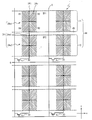
- FIG. 3 is a plan view of a part of the display panel shown in FIG.
- the scanning signal line driving circuit GD and the data signal line driving circuit SD are omitted for convenience of explanation.
- the display panel of the liquid crystal display device 1 has a gate line GL extending in the x direction and a source line SL extending in the y direction.
- a TFT 30 is provided in the vicinity of the intersection of the gate line GL and the source line SL.
- pixels of 2 rows and 2 columns are illustrated as a part of the pixel array.
- each of the pixel electrodes 24 has unit parts 24u1 and 24u2 and a connecting part 24n1.
- the unit parts 24u1 and 24u2 are arranged along the column direction (y direction).
- the connecting part 24n1 connects the unit part 24u1 and the unit part 24u2, and the potential of the unit part 24u1 is equal to the potential of the unit part 24u2.
- the display unit for displaying one color in the liquid crystal display device 1 includes two units arranged in parallel in the x direction and three units arranged in parallel in the y direction. A total of six unit portions are provided in a matrix.
- the unit parts 24u1 and 24u2 have the same shape.
- the unit 24u1 includes a cross-shaped shaft portion 24t and a stripe portion 24v extending from the shaft portion 24t.
- the four regions defined by the cross-shaped shaft portion 24t are defined as regions R1 to R4, and the horizontal direction (left and right direction) of the display screen (paper surface) is taken as the reference for the azimuth direction, and is positive counterclockwise (the display surface is In the case of a clock face, assuming that the 3 o'clock direction is an azimuth angle of 0 ° and the counterclockwise direction is positive), the stripe portions 24v of the regions R1 and R3 extend in an azimuth angle of 135 ° direction and an azimuth angle of 315 ° direction.
- the stripe portions 24v of the regions R2 and R4 extend in the azimuth angle 45 ° direction and the azimuth angle 225 ° direction.
- the unit parts 24u1 and 24u2 have a fishbone structure.
- the unit portions 24u1 and 24u2 each have a size of 45 ⁇ m ⁇ 45 ⁇ m, and the connecting portion 24n1 has a length of 5 ⁇ m.
- the width of the shaft portion 24t, the width of the stripe portion 24v, and the pitch of the stripe portion 24v are 4 ⁇ m, 2.5 ⁇ m, and 5.0 ⁇ m, respectively.
- FIG. 4 is a plan view of the counter substrate 40 on the side where the common electrode 44 is formed.
- the common electrode 44 is configured by the first common electrode 11 and the second common electrode 12, and the first common electrode 11 and the second common electrode 12 are the liquid crystal display device 1.
- the display areas 40D alternately extend linearly in the row direction (x direction).
- the width (length along the y direction) of each of the linear first common electrode 11 and the second common electrode 12 can be 145 ⁇ m, for example, and the width of the slit 45 can be 5 ⁇ m, for example.
- the first common electrode 11 and the second common electrode 12 are provided so as to overlap the pixel electrodes 24 arranged in one row, as shown in FIG. That is, the first common electrode 11 is disposed so as to overlap with the unit part 24 u 1 of a certain pixel electrode 24, and the second common electrode 12 is overlapped with the unit part 24 u 2 of the pixel electrode 24.
- a linear slit 45 is provided between the first common electrode 11 and the second common electrode 12 that alternately extend linearly in the row direction (x direction).
- the pixel P defined by the pixel electrode 24 is defined by the subpixel SP1 defined by the overlap between the unit portion 24u1 and the first common electrode 11, and the overlap between the unit portion 24u2 and the second common electrode 12. SP2 is included.
- each of the unit portions 24u1 and 24u2 functions as a subpixel electrode.
- the first common electrode 11 is electrically independent of the second common electrode 12, and a different common electrode signal is applied. That is, common electrode voltages having different voltage values are applied to the first common electrode 11 and the second common electrode 12.
- a common electrode signal applied to each common electrode is supplied from a common electrode signal application circuit provided in the external power supply circuit VGEN to a common electrode (COM) signal generation circuit (first common electrode voltage application means, second output) described later. It is generated through a common electrode voltage applying means).
- a signal (applied voltage) applied to the first common electrode 11 is referred to as a first common electrode signal (first common electrode voltage), and a signal applied to the second common electrode 12 ( The applied voltage) is called a second common electrode signal (second common electrode voltage).
- first common electrode signal may be referred to as a COM1 signal
- second common electrode signal may be referred to as a COM2 signal.
- the first common electrode signal is supplied to the first common electrode 11 via the wiring provided in the frame region 40S located on the left side of the display region 40D, and the second common electrode signal is supplied to the display region 40D. It is supplied to the second common electrode 12 via the wiring provided in the frame region 40S located on the right side.
- the first and second common electrode signals may be generated in an external circuit and input to the liquid crystal display device 1 via two COM terminals. Alternatively, the first and second common electrode signals may be generated in the driver.
- the liquid crystal molecules 62 of the liquid crystal layer 60 are aligned parallel to the direction in which the stripe portion 24v extends. At this time, the alignment of the liquid crystal molecules 62 is stabilized by the fishbone structure of the unit portions 24u1 and 24u2 shown in FIG. 3, and a liquid crystal domain is formed in each of the regions R1 to R4.
- the alignment direction of the liquid crystal molecules in the center of the liquid crystal domain is referred to as the reference alignment direction, and the azimuth component in the direction from the back surface to the front surface along the major axis of the liquid crystal molecules in the reference alignment direction (ie, the reference alignment The azimuth angle component whose direction is projected onto the main surface of the alignment film 26 or the alignment film 46 shown in FIG.
- the reference orientation characterizes the corresponding liquid crystal domain and has a dominant influence on the viewing angle characteristics of each liquid crystal domain.
- the reference alignment directions of the liquid crystal domains in the regions R1 to R4 are set so that the difference between any two directions is four directions substantially equal to an integral multiple of 90 °.
- the reference orientation directions of the liquid crystal domains in the regions R1 to R4 are 135 °, 45 °, 315 °, and 225 °, respectively. Thereby, a symmetric viewing angle characteristic is realized.
- the first common electrode signal is applied to the first common electrode 11, and the second common electrode signal different from the first common electrode signal is applied to the second common electrode 12. Since the potentials of the unit parts 24u1 and 24u2 of the pixel electrode 24 shown in FIG. 3 are equivalent to each other, the voltage applied to the liquid crystal layer 60 (FIG. 1) between the unit part 24u1 and the first common electrode 11 is unit. Unlike the voltage applied to the liquid crystal layer 60 (FIG. 1) between the portion 24u2 and the second common electrode 12, the transmittance of the sub-pixel SP1 is different from the transmittance of the sub-pixel SP2 in the intermediate gradation display.
- an input signal for making all the pixels have the same gradation level is input.
- the entire screen displays white.
- a voltage of 5 V is applied to the liquid crystal layer 60 (FIG. 1), the pixel has a transmittance corresponding to the maximum gradation level.
- the potential of the common electrode is adjusted instead of the pixel electrode in order to improve white floating.
- each common electrode voltage is controlled by controlling the application of the common electrode applied voltage to each common electrode (that is, the common electrode signal applied to each common electrode).
- (Potential) is inverted every integer multiple of the horizontal scanning period, and when the polarity inversion rises, the common electrode voltage is set to a certain voltage when the voltage starts to rise from a certain voltage to a predetermined voltage higher than the certain voltage.
- the falling point of polarity reversal is when the time point when the voltage starts to fall to a predetermined voltage lower than the certain voltage from (1) Between the rising edge of the polarity inversion of the first common electrode voltage and the rising edge of the polarity inversion of the second common electrode voltage in a certain horizontal scanning period; and (2) During the fall of the polarity inversion of the first common electrode voltage and the fall of the polarity inversion of the second common electrode voltage in the certain one horizontal scanning period, It is characterized by being configured to control so as to provide a time difference in at least one of the above.
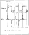
- FIG. 5 shows a signal timing chart ((a) in the figure) in each of the first common electrode 11 and the second common electrode 12 in this pattern, and a current waveform diagram (( b)).
- the amplitude of the first common electrode signal VC1 is smaller than the amplitude of the second common electrode signal VC2, and the first common electrode signal VC1
- the polarity inversion timing of the second common electrode signal VC2 is always delayed with respect to the polarity inversion timing. That is, in this pattern, the polarity inversion timing of the second common electrode signal VC2 is later than the polarity inversion timing of the first common electrode signal VC1 with respect to (1), and the second common electrode signal VC2 with respect to (2). Is later than the polarity inversion timing of the first common electrode signal VC1.
- the polarity inversion timing of the first common electrode signal VC1 is synchronized with the line inversion timing.
- the inrush current is time-axised by adopting this pattern in which the polarity inversion timing of the second common electrode signal VC2 is always delayed with respect to the polarity inversion timing of the first common electrode signal VC1. It can be seen that they are distributed along. That is, it can be said that this pattern is a driving method that can suppress the peak value (instantaneous value) of the current waveform to be lower than that of the comparison target.
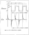
- FIG. 6 shows a signal timing chart ((a) in the figure) in each of the first common electrode 11 and the second common electrode 12 in this pattern, and a current waveform diagram along the timing chart (( b)).
- the amplitude of the first common electrode signal VC1 is smaller than the amplitude of the second common electrode signal VC2, and the second common electrode signal VC2
- the polarity inversion timing of the first common electrode signal VC1 is always delayed with respect to the polarity inversion timing. That is, in this pattern, the polarity inversion timing of the first common electrode signal VC1 is later than the polarity inversion timing of the second common electrode signal VC2 with respect to (1), and the first common electrode signal VC1 is also with respect to (2). Is later than the polarity inversion timing of the second common electrode signal VC2.
- the polarity inversion timing of the second common electrode signal VC2 is synchronized with the line inversion timing.
- the current waveform of the comparison target shown in FIG. 5 (b) is shown in addition to the current waveform along the timing chart of this pattern.
- the inrush current is time-axised by adopting this pattern in which the polarity inversion timing of the first common electrode signal VC1 is always delayed with respect to the polarity inversion timing of the second common electrode signal VC2. It can be seen that they are distributed along. That is, it can be said that this pattern is a driving method that can suppress the peak value (instantaneous value) of the current waveform to be lower than that of the comparison target.
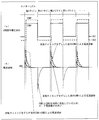
- FIG. 7 shows a signal timing chart ((a) in the figure) in each of the first common electrode 11 and the second common electrode 12 in this pattern, and a current waveform diagram (( b)).
- the amplitude of the first common electrode signal VC1 is smaller than the amplitude of the second common electrode signal VC2, and when the common electrode signal rises, The polarity inversion timing of the first common electrode signal VC1 is delayed with respect to the polarity inversion timing of the second common electrode signal VC2, and the second common with respect to the polarity inversion timing of the first common electrode signal VC1 when the common electrode signal falls.
- the polarity inversion timing of the electrode signal VC2 is delayed.
- the polarity inversion timing of the first common electrode signal VC1 is later than the polarity inversion timing of the second common electrode signal VC2 with respect to (1) above, and the second common electrode signal VC2 with respect to (2) above. Is later than the polarity inversion timing of the first common electrode signal VC1.
- the rising timing of the second common electrode signal VC2 is from one horizontal scanning period (n ⁇ 1 line) to the next one horizontal scanning period (n line).
- the falling timing of the first common electrode signal VC1 is synchronized with the switching from the nth line to the next n + 1th line when the common electrode signal falls.
- the current waveform of the comparison target shown in FIG. 5 (b) is shown in addition to the current waveform along the timing chart of this pattern.
- the inrush current is distributed along the time axis by shifting the polarity inversion timing of the first common electrode signal VC1 and the polarity inversion timing of the second common electrode signal VC2. Recognize. That is, it can be said that this pattern is a driving method that can suppress the peak value (instantaneous value) of the current waveform to be lower than that of the comparison target.
- FIG. 8 shows a signal timing chart ((a) in the figure) in each of the first common electrode 11 and the second common electrode 12 in this pattern, and a current waveform diagram along the timing chart (( b)).
- the amplitude of the first common electrode signal VC1 is smaller than the amplitude of the second common electrode signal VC2, and when the common electrode signal rises,
- the polarity inversion timing of the second common electrode signal VC2 is delayed with respect to the polarity inversion timing of the first common electrode signal VC1, and the first common with respect to the polarity inversion timing of the second common electrode signal VC2 when the common electrode signal falls.
- the polarity inversion timing of the electrode signal VC1 is delayed.
- the polarity inversion timing of the second common electrode signal VC2 is later than the polarity inversion timing of the first common electrode signal VC1 with respect to (1), and the first common electrode signal VC1 with respect to (2). Is later than the polarity inversion timing of the second common electrode signal VC2.
- the rising timing of the first common electrode signal VC1 is from one horizontal scanning period (n ⁇ 1 line) to the next one horizontal scanning period (nth line).
- the falling timing of the second common electrode signal VC2 is synchronized with the switching from the nth line to the next n + 1th line when the common electrode signal falls.
- the current waveform for comparison shown in FIG. 5B is shown in addition to the current waveform along the timing chart of this pattern.
- the inrush current is distributed along the time axis by shifting the polarity inversion timing of the first common electrode signal VC1 and the polarity inversion timing of the second common electrode signal VC2. Recognize. That is, it can be said that this pattern is a driving method that can suppress the peak value (instantaneous value) of the current waveform to be lower than that of the comparison target.
- FIG. 9 shows a signal timing chart ((a) in the figure) in each of the first common electrode 11 and the second common electrode 12 in this pattern, and a current waveform diagram (( b)).
- the amplitude of the first common electrode signal VC1 is smaller than the amplitude of the second common electrode signal VC2, and when the common electrode signal rises, The polarity inversion timing of the second common electrode signal VC2 is delayed with respect to the polarity inversion timing of the first common electrode signal VC1.
- the common electrode signal falls, the polarity of the first common electrode signal VC1 and the second common electrode signal VC2 is inverted at the same timing.
- the polarity reversal timing of the first common electrode signal VC1 is later than the polarity reversal timing of the second common electrode signal VC2 with respect to (1) above, and the first common at the same timing with respect to (2) above.
- the polarity of the electrode signal VC1 and the second common electrode signal VC2 is reversed.
- the rising timing of the second common electrode signal VC2 is from one horizontal scanning period (n ⁇ 1 line) to the next one horizontal scanning period (n line).
- the polarity inversion timing of the first common electrode signal VC1 and the second common electrode signal VC2 is switched from the nth line to the next n + 1th line when the common electrode signal falls. Synchronized.
- the current waveform for comparison shown in FIG. 5B is shown in addition to the current waveform along the timing chart of this pattern.
- the inrush current is distributed along the time axis by shifting the polarity inversion timing of the first common electrode signal VC1 and the polarity inversion timing of the second common electrode signal VC2. Recognize. That is, it can be said that this pattern is a driving method that can suppress the peak value (instantaneous value) of the current waveform to be lower than that of the comparison target.
- FIG. 10 shows a signal timing chart ((a) in the figure) in each of the first common electrode 11 and the second common electrode 12 in this pattern, and a current waveform diagram along the timing chart (( b)).
- the amplitude of the first common electrode signal VC1 is smaller than the amplitude of the second common electrode signal VC2, and when the common electrode signal rises, The polarity inversion timing of the first common electrode signal VC1 is delayed with respect to the polarity inversion timing of the second common electrode signal VC2.
- the common electrode signal falls, the polarity of the first common electrode signal VC1 and the second common electrode signal VC2 is inverted at the same timing.
- the definitions of “when the common electrode signal rises” and “when the common electrode signal falls” are the same as in the above ⁇ Pattern B >>.
- the polarity inversion timing of the second common electrode signal VC2 is later than the polarity inversion timing of the first common electrode signal VC1 with respect to (1) above, and the first common at the same timing with respect to (2) above.
- the polarity of the electrode signal VC1 and the second common electrode signal VC2 is reversed.
- the rising timing of the first common electrode signal VC1 is from one horizontal scanning period (n ⁇ 1 line) to the next one horizontal scanning period (nth line).
- the polarity inversion timing of the first common electrode signal VC1 and the second common electrode signal VC2 is switched from the nth line to the next n + 1th line when the common electrode signal falls. Synchronized.
- the current waveform of the comparison target shown in FIG. 5B is shown in addition to the current waveform along the timing chart of this pattern.
- the inrush current is distributed along the time axis by shifting the polarity inversion timing of the first common electrode signal VC1 and the polarity inversion timing of the second common electrode signal VC2. Recognize. That is, it can be said that this pattern is a driving method that can suppress the peak value (instantaneous value) of the current waveform to be lower than that of the comparison target.
- FIG. 11 shows a signal timing chart ((a) in the figure) in each of the first common electrode 11 and the second common electrode 12 in this pattern, and a current waveform diagram along the timing chart (( b)).
- the amplitude of the first common electrode signal VC1 is smaller than the amplitude of the second common electrode signal VC2, and when the common electrode signal rises, While the polarity of the first common electrode signal VC1 and the second common electrode signal VC2 is inverted at the same timing, the first common electrode signal VC1 with respect to the polarity inversion timing of the second common electrode signal VC2 when the common electrode signal falls.
- the polarity inversion timing is delayed. That is, in this pattern, the polarity of the first common electrode signal VC1 and the second common electrode signal VC2 is inverted at the same timing with respect to (1), and the polarity of the first common electrode signal VC1 with respect to (2).
- the inversion timing is later than the polarity inversion timing of the second common electrode signal VC2.
- the polarity inversion timing of the first common electrode signal VC1 and the second common electrode signal VC2 is the next one from a certain horizontal scanning period (the (n ⁇ 1) th line).
- the falling timing of the second common electrode signal VC2 is switched from the nth line to the next n + 1th line when the common electrode signal falls. Synchronized with.
- the current waveform of the comparison target shown in FIG. 5B is shown in addition to the current waveform along the timing chart of this pattern.
- the inrush current is distributed along the time axis by shifting the polarity inversion timing of the first common electrode signal VC1 and the polarity inversion timing of the second common electrode signal VC2. Recognize. That is, it can be said that this pattern is a driving method that can suppress the peak value (instantaneous value) of the current waveform to be lower than that of the comparison target.
- FIG. 12 shows a signal timing chart ((a) in the figure) in each of the first common electrode 11 and the second common electrode 12 in this pattern, and a current waveform diagram (( b)).
- the amplitude of the first common electrode signal VC1 is smaller than the amplitude of the second common electrode signal VC2, and when the common electrode signal rises, While the polarity of the first common electrode signal VC1 and the second common electrode signal VC2 is inverted at the same timing, the second common electrode signal VC2 with respect to the polarity inversion timing of the first common electrode signal VC1 when the common electrode signal falls.
- the polarity inversion timing is delayed. That is, in this pattern, the polarity of the first common electrode signal VC1 and the second common electrode signal VC2 is inverted at the same timing with respect to (1) above, and the polarity of the second common electrode signal VC2 with respect to (2) above.
- the inversion timing is later than the polarity inversion timing of the first common electrode signal VC1.
- the polarity inversion timing of the first common electrode signal VC1 and the second common electrode signal VC2 is the next one from a certain horizontal scanning period (the (n ⁇ 1) th line).
- the falling timing of the first common electrode signal VC1 is switched from the nth line to the next n + 1th line when the common electrode signal falls. Synchronized with.
- the current waveform of the comparison target shown in FIG. 5 (b) is shown in addition to the current waveform along the timing chart of this pattern.
- the inrush current is dispersed along the time axis by shifting the polarity inversion timing of the first common electrode signal VC1 and the polarity inversion timing of the second common electrode signal VC2. Recognize. That is, it can be said that this pattern is a driving method that can suppress the peak value (instantaneous value) of the current waveform to be lower than that of the comparison target.
- the polarity inversion signal output from the timing controller CTRL of the control device shown in FIG. 1 is input to the polarity inversion signal delay circuit A (control means) and the polarity inversion signal delay circuit B (control means) of the control device. After the processing, the signal is transmitted to a first common electrode signal (COM1 signal) generation circuit that generates a first common electrode signal and a second common electrode signal (COM2 signal) generation circuit that generates a second common electrode signal.
- COM1 signal first common electrode signal
- COM2 signal second common electrode signal
- the polarity inversion signal delay circuit A can select whether the operation is turned on or off by the control signal A shown in FIG. 1, and the polarity inversion signal delay circuit B is selected by the control signal B shown in FIG. It is possible to select whether the operation is turned on or off. According to this configuration, for example, when only the first common electrode signal VC1 is delayed as shown in FIG. 6, only the polarity inversion signal delay circuit A is operated using the control signal A, as shown in FIG. As described above, when only the second common electrode signal VC2 is delayed, only the polarity inversion signal delay circuit B needs to be operated using the control signal B. In addition, according to the configuration shown in FIG. 1, it is possible to select a common electrode signal that is delayed at the time of rising and / or falling.
- the time difference is preferably a time obtained by subtracting the time during which a voltage is applied to the gate electrode provided in the TFT 30 (FIG. 1) from the time of one horizontal scanning period at the longest. This is because if the writing (charging) period to the pixel and the inversion time of the common electrode voltage overlap, charging may be insufficient. However, by setting the time difference as described above, the writing (charging) period to the pixel does not overlap with the inversion time of the common electrode voltage, so that insufficient charging does not occur.
- FIG. 13 shows a circuit block configuration to be compared.
- the polarity inversion signal delay circuit A and the polarity inversion signal delay circuit B in FIG. 1 of this embodiment are not provided, and the polarity inversion signal output from the timing controller CTRL is the COM1 signal ( The first common electrode signal) and the COM2 signal (second common electrode signal) generation circuit are input to the polarity inversion signal to determine the polarity of the first common electrode signal and the second common electrode signal. Output to the electrode.
- the polarities (High or Low) of the first common electrode signal and the second common electrode signal are switched in synchronization with the switching of the polarity inversion signal between High and Low (however, the phases may be reversed) is there).
- both the first common electrode signal VC1 and the second common electrode signal VC2 can be delayed, and all the above-described patterns can be realized with the configuration of FIG. .
- both the first common electrode signal VC1 and the second common electrode signal VC2 can be delayed, and all the above-described patterns can be realized with the configuration of FIG. .
- a time difference is provided at the start of polarity inversion of each common electrode signal.
- the time difference (shift amount) at the start of polarity reversal of each common electrode signal can be a period that is an integral multiple of a period that is half of the reference clock used in the liquid crystal display device 1 (FIG. 1).
- FIG. 14 shows an example in which the polarity of the second common electrode signal VC2 is inverted behind the first common electrode signal VC1 when the common electrode signal rises.
- FIG. 14 by setting the start of polarity reversal to a period that is an integral multiple of half the period of the reference clock, the timing adjustment at the rise and / or fall of polarity reversal can be simplified as a result. It can be realized with a circuit.
- FIG. 15 shows a circuit configuration for realizing FIG. 14 by using a part of FIG.
- a clock signal of a video interface inputted to the liquid crystal display device 1 can be used.
- the present invention can be realized with a simple circuit configuration.
- an internal oscillation clock signal (cks, ckg in FIG. 1) generated by the liquid crystal display device 1 (FIG. 1) can be used as the reference clock.
- the present invention can be realized with a simple circuit configuration.
- the polarity inversion signal is input to the inverter delay circuit as shown in FIG.
- the second common electrode signal VC2 by passing through the inverter delay circuit Is delayed.
- the buffer circuit is provided on the circuit (common electrode signal generation circuit) side that generates the common electrode signal to be delayed, and the polarity inversion signal is first input to the buffer circuit. It is also possible to configure so that the polarity inversion signal is delayed by passing through a plurality of stages of the buffer circuit.
- the liquid crystal display device 1 of the present embodiment is at least at the time of rising of polarity inversion and the falling of polarity inversion of each common electrode voltage in a certain horizontal scanning period.
- control means a timing controller CTRL and polarity reversal in FIG. 1 controls to provide a time difference between the polarity inversion timing of the first common electrode voltage and the polarity inversion timing of the second common electrode voltage.
- Signal delay circuits A and B are provided.
- the polarities of the first and second common electrode voltages are not reversed all at once, and the time differences (shifts) exemplified in the patterns A to H are provided at the timing. Due to this time difference, the peak value (instantaneous value) of the current waveform can be dispersed along the time axis, and the peak value does not concentrate at a certain point in time.
- a liquid crystal display device having a wide viewing angle characteristic in which a plurality of sub-pixels are provided with a plurality of common electrodes facing each pixel electrode, it is possible to suppress an increase in current required for polarity inversion of the common electrode voltage. it can.
- the polarity inversion timing is shifted every horizontal scanning period.
- the present invention is not limited to this, and may be every two horizontal scanning periods. It is also possible to adjust the timing as described above for each integer multiple.
- the present invention is not limited to the horizontal scanning period, and the present invention is also effective to perform the same timing adjustment at the time of polarity reversal in the blanking period of the vertical scanning period.
- the liquid crystal display device operating in the VA mode is illustrated, but the present invention is not limited to this, and may be a liquid crystal display device operating in the TN mode, or the pixel electrode. And a common electrode in the same plane and a liquid crystal display device operating in the IPS mode.
- a predetermined low voltage The potential continuously changes from the level (predetermined low potential) to the predetermined high voltage level (potential).
- a predetermined high (low) voltage level is changed from a predetermined low (high) voltage level at the time of polarity reversal of at least one common electrode signal of the first common electrode signal and the second common electrode signal. The transition until is divided into a plurality of transition periods, and the timing of polarity inversion is different between that of the first common electrode signal and that of the second common electrode signal signal.
- the transition is divided into a plurality of transition periods at the time of polarity reversal means that the voltage level (potential) for a predetermined period at a voltage level in the middle from a predetermined low (high) voltage level to a predetermined high (low) voltage level. ) Is a period in which no transition occurs.
- the mode divided into the plurality of transition periods may be only at the time of rising ((1) described in the first embodiment) or only at the time of falling ((2) described in the first embodiment).
- both of the rising time and the falling time both (1) and (2) described in the first embodiment may be used.
- the method of performing polarity reversal by dividing into a plurality of transition periods can be realized by adopting a conventionally known method.
- FIG. 17 shows a signal timing chart ((a) in the figure) in each of the first common electrode 11 and the second common electrode 12 in this pattern, and a current waveform diagram along the timing chart (( b)).
- the second common electrode signal VC2 passes through a predetermined transition from a predetermined low voltage level (predetermined low potential) through two transition periods. Transition to a high voltage level (potential). Then, the polarity inversion timing in the latter stage of the two-stage transition period of the second common electrode signal VC2 is delayed from the polarity inversion of the first common electrode signal VC1, but the two-stage transition period. The polarity inversion timing in the previous stage is earlier than the polarity inversion of the first common electrode signal VC1.
- the start of the polarity inversion of the second common electrode signal VC2 is ahead of the start of the polarity inversion of the first common electrode signal VC1.
- the second common electrode signal VC2 reaches a predetermined high voltage level (that is, polarity inversion is completed)
- the first common electrode signal VC1 has already reached the predetermined high voltage level (that is, polarity inversion is completed). ing.
- this pattern can be applied not only at the time of rising but also at the time of falling.
- the advantage of this pattern is that, as shown in FIG. 17B, the peak value of the inrush current at the time of rising can be further reduced.
- the polarity inversion timing is completely shifted between the first common electrode signal VC1 and the second common electrode signal VC2, thereby reversing the polarity at the same timing.
- the peak current value is kept low compared with the comparative configuration of 13
- the peak value of the inrush current due to the second common electrode signal VC2 is caused by the difference in amplitude between the first common electrode signal VC1 and the second common electrode signal VC2. , Larger than that of the first common electrode signal VC1.
- the timing of the polarity inversion of the first common electrode signal VC1 is completely different from that of the second common electrode signal VC2 having a larger amplitude than the first common electrode signal VC1, and By controlling the transition so as to be divided into a plurality of transition periods, the peak value of the inrush current can be further reduced.
- FIG. 18 shows a signal timing chart ((a) in the figure) in each of the first common electrode 11 and the second common electrode 12 in this pattern and a current waveform diagram (( b)).
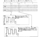
- the timing of polarity inversion of the common electrode signal is made different or the same timing periodically or non-periodically (randomly) in a continuous horizontal scanning period.
- the first common electrode signal VC1 and the second common electrode signal VC1 are the same pattern in all lines.
- the timing of polarity inversion with respect to the common electrode signal VC2 is shifted, in the present embodiment, when changing the timing, any one of the above-mentioned ⁇ Pattern A >> to ⁇ Pattern J >> is selected and the horizontal scanning period is selected. It is characterized in that the selection is switched every time (or every successive horizontal scanning periods).
- FIG. 19 is an example of this embodiment.
- FIG. 19A is a signal timing chart over a plurality of continuous horizontal scanning periods in each of the first common electrode 11 and the second common electrode 12, and
- FIG. 19B is a timing chart according to the timing chart. It is a current waveform diagram.
- the polarity inversion timing is shifted after a certain horizontal scanning period (the nth line), but it is not always necessary to switch every line.
- the n, n + 1, and n + 2 lines have the same polarity, such that the polarity inversion timing is shifted in a certain same pattern, and the n + 3 line has the polarity inversion timing shifted in a different pattern from the same pattern.
- a plurality of lines may be continued as a reverse pattern.
- a location where the polarity of the first common electrode signal VC1 and the second common electrode signal VC2 is inverted at the same timing may be provided in any line.
- this embodiment demonstrated the aspect which selects a pattern for every line (or for every several continuous lines), it is not limited to this, For every frame (or for every several continuous frames) Alternatively, the polarity inversion timing pattern may be selected. Hereinafter, this aspect will be described.
- FIG. 20 is another example of this embodiment.
- one of the same patterns as ⁇ Pattern A >> to ⁇ Pattern G >> in the first embodiment is selected, and the selection is switched for each frame.
- the polarity inversion timing of the common electrode signal is different between the (m + 1) th frame and the (m + 2) th frame, but it is not always necessary to switch every frame (continuous frame). That is, the polarity inversion timing is shifted in a certain same pattern in the m, m + 1, and m + 2 frames, and the polarity inversion timing is shifted in a different pattern from the same pattern in the m + 3 frame.
- a plurality of frames may be the reverse pattern.
- FIG. 20 although comprised by two patterns, it is not limited to two, You may combine three or more different timing patterns. Further, in a certain frame, a frame in which the polarity of the first common electrode signal VC1 and the second common electrode signal VC2 is inverted at the same timing may be provided.
- the timing caused by the current change caused by the polarity inversion does not occur periodically as in the case of line units, so that the liquid crystal display device 1 ( Since the unnecessary radiation emitted by FIG. 1) is dispersed in frequency, the peak value of the unwanted radiation intensity can be reduced.
- the present invention has been made in view of the above problems, and an object of the present invention is to provide a liquid crystal display device in which the current value of an instantaneous inrush current when the polarity of a COM signal (COM voltage) is reversed is reduced. It is in.
- the liquid crystal display device includes: An active matrix in which a plurality of data signal lines and a plurality of scanning signal lines intersecting the data signal lines are formed, and an active element and a pixel electrode are arranged at each intersection of the data signal line and the scanning signal line A substrate, A counter substrate disposed opposite to the active matrix substrate; A plurality of common electrodes disposed on the active matrix substrate or the counter substrate; A liquid crystal layer disposed between the active matrix substrate and the counter substrate; Each of the plurality of pixel electrodes includes a region facing the first common electrode of the plurality of common electrodes, and a second of the plurality of common electrodes different from the first common electrode.
- a liquid crystal display device in which a region facing the common electrode is formed, First common electrode voltage applying means for applying a first common electrode voltage to the first common electrode; A second common electrode voltage applying means for applying a second common electrode voltage having a voltage value different from the first common electrode voltage to the second common electrode; Control means for controlling the application of the common electrode applied voltage to each common electrode by the first common electrode voltage applying means and the second common electrode voltage applying means and inverting the polarity of each common electrode voltage every certain period And When each common electrode voltage starts to rise from a certain voltage to a predetermined voltage higher than the certain voltage due to polarity reversal, at the rising edge of polarity reversal, each common electrode voltage changes from a certain voltage to a certain voltage due to polarity reversal.
- the control means includes (1) Between a rising edge of the polarity reversal of the first common electrode voltage and a rising edge of the polarity reversal of the second common electrode voltage in a certain period; and (2) Between the fall of the polarity reversal of the first common electrode voltage and the fall of the polarity reversal of the second common electrode voltage in the certain period, It is characterized by being configured to control so as to provide a time difference in at least one of the above.
- the liquid crystal display device can provide a liquid crystal display device in which the current value of the instantaneous inrush current when the polarity of the COM signal (COM voltage) is reversed is reduced.
- COM signal COM voltage
- a description will be given by taking as an example a case where a common electrode is disposed on the counter substrate.
- each of the plurality of pixel electrodes has a region facing the first common electrode among the plurality of common electrodes with the liquid crystal layer interposed therebetween, and a plurality of the plurality of pixel electrodes with the liquid crystal layer interposed therebetween.
- the common electrode is formed with a region facing the second common electrode different from the first common electrode, and the first common electrode and the second common electrode are different from each other.
- a common electrode voltage is applied.
- each pixel electrode includes at least a first region facing the first common electrode with the liquid crystal layer interposed therebetween, and a second region facing the second common electrode with the liquid crystal layer interposed therebetween. Will have.
- the first common electrode voltage is applied to the first common electrode
- the second common electrode voltage is applied to the second common electrode.
- the liquid crystal layer in the first region that is, the first region of the pixel electrode and the first common electrode voltage are different from each other.
- the liquid crystal layer sandwiched between the common electrode and the liquid crystal layer in the second region that is, the liquid crystal layer sandwiched between the second region of the pixel electrode and the second common electrode. The voltage can be made different.
- the display screen of the liquid crystal display device is inclined in the middle direction.
- the display quality when viewed from above can be improved. That is, the viewing angle characteristics of the liquid crystal display device can be improved.
- the amplitude of either the first common electrode voltage (COM1) applied to the first common electrode or the second common electrode voltage (COM2) applied to the second common electrode is set to the common electrode voltage (although it has the effect of widening the viewing angle by expanding it from the amplitude of (COM), there arises a problem that the inrush current generated when the COM signal is inverted increases.
- the configuration (1) having COM1 and COM2 as compared with the configuration (1) in which the COM amplitude is 5 Vpp the COM1 amplitude is 4 Vpp and the COM2 amplitude is 8.5 Vpp.
- the timing of the polarity inversion of the first common electrode voltage at least one of the rising edge of the polarity inversion of each common electrode voltage and the falling edge of the polarity inversion in a certain horizontal scanning period.
- liquid crystal display device having a wide viewing angle characteristic that achieves low power consumption by suppressing the occurrence of inconvenient inrush current at a low cost.
- the configuration of the present invention a wide viewing angle characteristic is realized and the instantaneous inrush current value (peak value) at the time of polarity reversal of the common electrode voltage, which has been a problem in the conventional configuration, can be reduced. Can do.
- the polarity is an expression relatively indicating the relationship between the common electrode potential and the source potential during the period in which the voltage is applied to the pixel electrode, and the source potential level is relatively higher than the common electrode potential.
- the state is called positive polarity, and the state where the source potential level is relatively low with respect to the common electrode potential is called negative polarity.
- the control means may be configured to control so as to delay the polarity inversion of the first common electrode voltage with respect to the polarity inversion of the second common electrode voltage with respect to the time difference.
- the liquid crystal display device can delay the polarity inversion timing of the first common electrode voltage and disperse the peak value (instantaneous value) of the current waveform along the time axis. it can.
- the polarity inversion (voltage change) of the common electrode with a small amplitude is completed in a shorter time. Therefore, by delaying the start timing of the common electrode having a small amplitude, it becomes possible to roughly align the time points when both the common electrodes have risen. That is, the time for applying a predetermined voltage from the common electrode to the first and second regions can be made equal.
- the liquid crystal display device has the above configuration,
- the amplitude of the first common electrode voltage is smaller than the amplitude of the second common electrode voltage,
- the control means is preferably configured to control so as to delay the polarity inversion of the second common electrode voltage with respect to the polarity inversion of the first common electrode voltage with respect to the time difference.
- the liquid crystal display device can delay the polarity inversion timing of the second common electrode voltage and disperse the peak value (instantaneous value) of the current waveform along the time axis. it can.
- the liquid crystal display device has the above configuration,
- the control means is configured to control both (1) and (2), With respect to the time difference, the polarity inversion of the first common electrode voltage is delayed with respect to the polarity inversion of the second common electrode voltage at the time of rising of the polarity inversion, and the first inversion at the time of falling of the polarity inversion. It is preferable to control so as to delay the polarity inversion of the second common electrode voltage with respect to the polarity inversion of the common electrode voltage.
- the peak value (instantaneous value) of the current waveform can be dispersed along the time axis as described above.
- the peak value of the current in terms of frequency band can be reduced, so that the inversion periods of COM1 and COM2 are the EMI can be effectively suppressed as compared with the above-described aspect that is the same at the time of falling.
- the control means is configured to control both (1) and (2), With respect to the time difference, when the polarity inversion rises, the polarity inversion of the second common electrode voltage is delayed with respect to the polarity inversion of the first common electrode voltage, and when the polarity inversion falls, the second inversion
- the polarity inversion of the first common electrode voltage may be controlled to be delayed with respect to the polarity inversion of the common electrode voltage.
- the control means is configured to perform the control of (1) out of (1) and (2), and with respect to the time difference, with respect to polarity inversion of the second common electrode voltage, Control to delay the polarity reversal of the first common electrode voltage; At the fall of the polarity inversion, the control means may perform control so that the polarity inversion of the first common electrode voltage and the polarity inversion of the second common electrode voltage are performed at the same timing.
- the control means is configured to perform the control of (1) out of the above (1) and (2), and with respect to the time difference, with respect to the polarity inversion of the first common electrode voltage, Control to delay the polarity inversion of the second common electrode voltage, At the fall of the polarity inversion, the control means may perform control so that the polarity inversion of the first common electrode voltage and the polarity inversion of the second common electrode voltage are performed at the same timing.
- the control means is configured to perform the control of (2) out of (1) and (2) above, and the second common electrode at the falling edge of the polarity reversal with respect to the time difference. Control to delay the polarity inversion of the first common electrode voltage with respect to the polarity inversion of the voltage, At the rising edge of the polarity inversion, the control means may perform control so that the polarity inversion of the first common electrode voltage and the polarity inversion of the second common electrode voltage are performed at the same timing.
- the control means is configured to perform the control of the above (2) of the above (1) and (2), and the first common electrode at the falling edge of the polarity inversion with respect to the time difference. Control to delay the polarity reversal of the second common electrode voltage with respect to the voltage reversal of voltage, At the rising edge of the polarity inversion, the control means may perform control so that the polarity inversion of the first common electrode voltage and the polarity inversion of the second common electrode voltage are performed at the same timing.
- the liquid crystal display device has the above configuration,
- the control means can provide the time difference based on a preset timing signal.
- a timing signal used for image display for example, a clock signal described later
- a preset timing signal there is no need to separately provide a clock signal for adjusting the polarity inversion timing.
- the circuit configuration can be used, and the liquid crystal display device according to the present invention can be realized without requiring a complicated circuit configuration.
- the liquid crystal display device includes:
- the timing signal is preferably a clock signal output from a transmitter provided in the display device.
- the existing circuit configuration can be used, and the liquid crystal display device according to the present invention can be realized without requiring a complicated circuit configuration.
- the timing signal may be a clock signal input from an external device of the display device.
- the existing circuit configuration can be used, and the liquid crystal display device according to the present invention can be realized without requiring a complicated circuit configuration.
- the liquid crystal display device has the above configuration, It is preferable that the time difference is a period that is an integral multiple of one-half the period of the clock signal.
- the inversion timing is delayed in a period that is an integral multiple of one-half the period of the clock signal, a simple circuit can be used.
- the liquid crystal display device has the above configuration,
- the time difference is preferably a delay period when the clock signal passes through a plurality of stages of inverters or buffer circuits provided in the display device.
- the liquid crystal display device has the above configuration, Even if the time difference is long, it is preferable to subtract the time during which a voltage is applied to the gate electrode provided in the active element from the time of the certain period.
- the writing (charging) period to the pixel overlaps with the inversion time of the common electrode voltage, charging may be insufficient.
- the writing (charging) period to the pixel is set by setting the time difference as described above.
- the inversion times of the common electrode voltage do not overlap, there is no shortage of charging.
- the liquid crystal display device has the above configuration,
- the control means controls the second common electrode voltage so that the transition period from the potential level immediately before the polarity inversion to the potential level at the time when the polarity inversion is completed is divided into a plurality of transition periods. It is preferable.
- the liquid crystal display device has the above configuration, In the intermediate period among the plurality of transition periods, the control means has at least one period in which the potential level of the second common electrode voltage is the potential level immediately before the polarity inversion of the first common electrode voltage. It is preferable to control so that there is a period.
- the liquid crystal display device has the above configuration,
- the control means has a timing at which all of the plurality of transition periods are different from a timing at which the polarity of the first common electrode voltage is inverted from a potential level immediately before the polarity inversion to a potential level at the time when the polarity inversion is completed. It is preferable to make transition at.
- the liquid crystal display device has the above configuration, For each of the first common electrode voltage and the second common electrode voltage, the control means sets a plurality of transition periods from a potential level immediately before polarity reversal to a potential level at the time of completion of polarity reversal. It is preferable to control the transition so as to be divided into transition periods.
- the liquid crystal display device has the above configuration, It is preferable that the control means includes a switching means for switching between (1), (2), and (1) and (2) at every certain period. .
- the liquid crystal display device has the above configuration,
- the operation mode is preferably the VA mode.
- the liquid crystal display device can make the certain period an integral multiple of the horizontal scanning period.
- the certain period may be a blanking period of the vertical scanning period.
- the present invention can be suitably used for various devices that use a liquid crystal display device as a display unit, such as a television and a portable terminal.
Landscapes
- Engineering & Computer Science (AREA)
- Power Engineering (AREA)
- Chemical & Material Sciences (AREA)
- Crystallography & Structural Chemistry (AREA)
- Physics & Mathematics (AREA)
- Computer Hardware Design (AREA)
- General Physics & Mathematics (AREA)
- Theoretical Computer Science (AREA)
- Control Of Indicators Other Than Cathode Ray Tubes (AREA)
- Liquid Crystal (AREA)
Abstract
本発明に係る液晶表示装置(1)は、表示パネルの1画素領域中に第1共通電極(11)および第2共通電極(12)を有しており、それぞれに入力される第1共通電極信号と第2共通電極信号とを水平走査期間ごとに極性反転させる際に第1共通電極信号の極性反転タイミングと第2共通電極信号の極性反転タイミングとをずらすための遅延回路(A・B)を具備する。よって、本発明によれば、広視野角特性を実現している表示装置において、共通電極信号(共通電極電圧)の極性反転時のピークの突入電流を低減させた液晶表示装置を提供する。
Description
本発明は、交流駆動を行う液晶パネルの駆動方法とそれを用いた液晶表示装置に関する。
液晶パネルの駆動方法としては、ソースドライバから出力されて画素電極に印加されるデータ信号電圧レベルと、共通電極信号生成回路から出力されて共通電極に印加される共通電極電圧レベルを、ある一定期間毎に反転させる交流駆動を行うことが一般的であるが、交流駆動を行うと、その極性反転のタイミングにおいて、液晶容量に対する突入電流が生じるという課題がある。
そのため、データ信号電圧や共通電極電圧を出力する回路から見た場合に負荷が重たくなる大型液晶パネルや高解像度の液晶パネルに対しては、複数のソースドライバを搭載して、その複数のドライバ毎に極性を反転させるタイミングを異ならしめて、突入電流を低減させている。
例えば、特許文献1は、一つの液晶パネルに対して、複数組のソースドライバやゲートドライバによって駆動する構成について記載している。当該構成では、少なくとも2つのグループに分割駆動される液晶パネルに対して、液晶パネルの各グループに印加される各駆動電圧の交流化タイミングを、各グループ毎に異ならしめることによって、全画素に印加されているバイアス電圧の極性を一斉に反転させる構成と比較して、液晶パネル容量に流れる突入電流(ラッシュ電流)の低減化を実現している。
しかしながら、上記の従来構成であっても、突入電流が充分低減できておらず、また、ソースドライバやゲートドライバがそれぞれ一つずつの構成の場合には有効な手段ではないため、更なる低減化が求められている。
そこで本願発明者らは、COM信号の反転時(COM電圧の極性反転時)に、COM信号ラインに突入電流が流れる点に着目し、COM信号の反転機構について改善することにより、突入電流がより一層低減できることを見出した。
本発明は、上記の問題点に鑑みてなされたものであり、その目的は、COM信号(COM電圧)の極性反転時の瞬時の突入電流の電流値を低減させた液晶表示装置を提供することにある。
すなわち、上記の課題を解決するために、本発明に係る液晶表示装置は、
複数のデータ信号線と該データ信号線に交差する複数の走査信号線とが形成されると共に、データ信号線と走査信号線の各交差部に能動素子と画素電極とがそれぞれ配されたアクティブマトリクス基板と、
上記アクティブマトリクス基板に対向して配置される対向基板と、
上記アクティブマトリクス基板あるいは上記対向基板に配された複数の共通電極と、
上記アクティブマトリクス基板と上記対向基板との間に配置される液晶層とを備えており、
該複数の画素電極のそれぞれに、該複数の共通電極のうちの第1の共通電極と対向している領域と、該複数の共通電極のうちの、第1の共通電極とは異なる第2の共通電極と対向している領域とが形成されている液晶表示装置であって、
上記第1の共通電極に対して、第1の共通電極電圧を印加する第1共通電極電圧印加手段と、
上記第2の共通電極に対して、上記第1の共通電極電圧とは異なる電圧値である第2の共通電極電圧を印加する第2共通電極電圧印加手段と、
上記第1共通電極電圧印加手段および上記第2共通電極電圧印加手段による各共通電極への共通電極印加電圧の印加を制御して、各共通電極電圧の極性を或る期間ごとに反転させる制御手段とを備えており、
各共通電極電圧が極性反転によって、或る電圧から該或る電圧よりも高い所定の電圧へ立ち上がり始める時点を極性反転の立ち上がり時、各共通電極電圧が極性反転によって、或る電圧から該或る電圧よりも低い所定の電圧へ立ち下がり始める時点を極性反転の立ち下がり時としたとき、
上記制御手段は、
(1) 或る期間における、上記第1の共通電極電圧の上記極性反転の立ち上がり時と、上記第2の共通電極電圧の上記極性反転の立ち上がり時との間、および、
(2) 上記或る期間における、上記第1の共通電極電圧の上記極性反転の立ち下がり時と、上記第2の共通電極電圧の上記極性反転の立ち下がり時との間、
の少なくとも一方に、時間差を設けるように制御するように構成されていることを特徴としている。
複数のデータ信号線と該データ信号線に交差する複数の走査信号線とが形成されると共に、データ信号線と走査信号線の各交差部に能動素子と画素電極とがそれぞれ配されたアクティブマトリクス基板と、
上記アクティブマトリクス基板に対向して配置される対向基板と、
上記アクティブマトリクス基板あるいは上記対向基板に配された複数の共通電極と、
上記アクティブマトリクス基板と上記対向基板との間に配置される液晶層とを備えており、
該複数の画素電極のそれぞれに、該複数の共通電極のうちの第1の共通電極と対向している領域と、該複数の共通電極のうちの、第1の共通電極とは異なる第2の共通電極と対向している領域とが形成されている液晶表示装置であって、
上記第1の共通電極に対して、第1の共通電極電圧を印加する第1共通電極電圧印加手段と、
上記第2の共通電極に対して、上記第1の共通電極電圧とは異なる電圧値である第2の共通電極電圧を印加する第2共通電極電圧印加手段と、
上記第1共通電極電圧印加手段および上記第2共通電極電圧印加手段による各共通電極への共通電極印加電圧の印加を制御して、各共通電極電圧の極性を或る期間ごとに反転させる制御手段とを備えており、
各共通電極電圧が極性反転によって、或る電圧から該或る電圧よりも高い所定の電圧へ立ち上がり始める時点を極性反転の立ち上がり時、各共通電極電圧が極性反転によって、或る電圧から該或る電圧よりも低い所定の電圧へ立ち下がり始める時点を極性反転の立ち下がり時としたとき、
上記制御手段は、
(1) 或る期間における、上記第1の共通電極電圧の上記極性反転の立ち上がり時と、上記第2の共通電極電圧の上記極性反転の立ち上がり時との間、および、
(2) 上記或る期間における、上記第1の共通電極電圧の上記極性反転の立ち下がり時と、上記第2の共通電極電圧の上記極性反転の立ち下がり時との間、
の少なくとも一方に、時間差を設けるように制御するように構成されていることを特徴としている。
上記の構成によれば、本発明に係る液晶表示装置は、COM信号(COM電圧)の極性反転時の瞬時の突入電流の電流値を低減させた液晶表示装置を提供することができる。以下では対向基板に共通電極が配された場合を例にして説明を行う。
まず、本発明に係る液晶表示装置は、複数の画素電極のそれぞれに、液晶層を挟んで複数の共通電極のうちの第1の共通電極と対向している領域と、液晶層を挟んで複数の共通電極のうちの、第1の共通電極とは異なる第2の共通電極と対向している領域とが形成されており、第1の共通電極と、第2の共通電極とには互いに異なる共通電極電圧が印加されるように構成されている。これにより、各画素電極は、少なくとも、液晶層を挟んで第1の共通電極と対向している第1の領域、および液晶層を挟んで第2の共通電極と対向している第2の領域を有することになる。液晶表示装置が駆動する際、第1の共通電極には第1の共通電極電圧が印加され、第2の共通電極には第2の共通電極電圧が印加される。ここで、上記のように、第1の共通電極電圧と第2の共通電極電圧とは互いに異なる電圧値であるため、第1の領域における液晶層、すなわち画素電極の第1の領域と第1の共通電極とに挟まれた液晶層に印加される電圧と、第2の領域における液晶層、すなわち画素電極の第2の領域と第2の共通電極とに挟まれた液晶層に印加される電圧とを相違させることができる。
しかも、液晶表示装置のV-T特性は、画素内の各領域の、領域ごとに相違する透過率を平均化したものに基づくものなので、中間階調において、液晶表示装置の表示画面を斜め方向から見た場合の表示品位を向上させることができる。すなわち、液晶表示装置の視野角特性を改善できる。
ところで、第1の共通電極に印加する第1の共通電極電圧(COM1)か第2の共通電極に印加する第2の共通電極電圧(COM2)のどちらかの振幅を従来構成の共通電極電圧(COM)の振幅より拡げることで視野角を広げる効果があるが、COM信号の反転時に生じる突入電流が増えてしまうという問題が生じる。例えば、従来、COM振幅が5Vppである構成(1)に対して、COM1およびCOM2を具備する構成(2)では、COM1振幅が4VppでCOM2振幅が8.5Vppとなる。この場合、COM信号の反転時に必要な電流を下記の式;
電流=f×C×Vpp
(f:反転周波数、C:液晶容量、Vpp:COM振幅)
に基づけば、
上記構成(1)=f×C×5=5fC
上記構成(2)=f×C/2×4+f×C/2×8.5=6.25fC
となり、上記構成(2)においてCOM信号の反転時に必要な電流が増えてしまうことがわかる。また、この不都合な突入電流の発生に備えて、システム側では、突入電流が流れてしまっても電源が落ちないように、突入電流値に対して充分な電流供給能力を備える必要がある。すなわち、突入電流に備えて、システム側の電源設計上、コスト高の部品を使用する必要がある。しかしながら、本発明によれば、或る1水平走査期間における、各共通電極電圧の極性反転の立ち上がり時および極性反転の立ち下がり時の少なくとも一方の時に、第1の共通電極電圧の極性反転のタイミングと、第2の共通電極電圧の極性反転のタイミングとに時間差を設けるように制御する制御手段を備えている。これにより、第1および第2の共通電極電圧の極性は、一斉に反転せず、そのタイミングにずれを設けている。この時間差により、電流波形のピーク値(瞬間値)を時間軸に沿って分散させることができ、ピーク値が或る時点に集中することがない。
電流=f×C×Vpp
(f:反転周波数、C:液晶容量、Vpp:COM振幅)
に基づけば、
上記構成(1)=f×C×5=5fC
上記構成(2)=f×C/2×4+f×C/2×8.5=6.25fC
となり、上記構成(2)においてCOM信号の反転時に必要な電流が増えてしまうことがわかる。また、この不都合な突入電流の発生に備えて、システム側では、突入電流が流れてしまっても電源が落ちないように、突入電流値に対して充分な電流供給能力を備える必要がある。すなわち、突入電流に備えて、システム側の電源設計上、コスト高の部品を使用する必要がある。しかしながら、本発明によれば、或る1水平走査期間における、各共通電極電圧の極性反転の立ち上がり時および極性反転の立ち下がり時の少なくとも一方の時に、第1の共通電極電圧の極性反転のタイミングと、第2の共通電極電圧の極性反転のタイミングとに時間差を設けるように制御する制御手段を備えている。これにより、第1および第2の共通電極電圧の極性は、一斉に反転せず、そのタイミングにずれを設けている。この時間差により、電流波形のピーク値(瞬間値)を時間軸に沿って分散させることができ、ピーク値が或る時点に集中することがない。
よって、複数の共通電極を各画素電極に対向させて副画素を複数設けた広視野角特性を有する液晶表示装置において、共通電極電圧の極性反転時に必要な電流が増えることを抑制することができる。
また、このように本発明の構成によれば、不都合な突入電流の発生が抑えられることから、システム側での電源設計に関してコスト高の部品を使用する必要がない。
すなわち、不都合な突入電流の発生を抑えることで低消費電力を実現した広視野角特性を有する液晶表示装置を、低コストで提供することができる。
したがって、本発明の構成によれば、広視野角特性を実現するとともに、従来構成において問題となっていた共通電極電圧の極性反転時の瞬時の突入電流の電流値(ピーク値)を低減させることができる。
なお、極性とは、画素電極に電圧を印加している期間の、共通電極電位とソース電位の関係を相対的に示した表現であり、共通電極電位に対してソース電位レベルが相対的に高い状態を正極性、共通電極電位に対してソース電位レベルが相対的に低い状態を負極性という。
本発明の他の目的、特徴、および優れた点は、以下に示す記載によって十分分かるであろう。また、本発明の利点は、添付図面を参照した次の説明で明白になるであろう。
以上のように、本発明に係る液晶表示装置は、
複数のデータ信号線と該データ信号線に交差する複数の走査信号線とが形成されると共に、データ信号線と走査信号線の各交差部に能動素子と画素電極とがそれぞれ配されたアクティブマトリクス基板と、
上記アクティブマトリクス基板に対向して配置される対向基板と、
上記アクティブマトリクス基板あるいは上記対向基板に配された複数の共通電極と、
上記アクティブマトリクス基板と上記対向基板との間に配置される液晶層とを備えており、
該複数の画素電極のそれぞれに、該複数の共通電極のうちの第1の共通電極と対向している領域と、該複数の共通電極のうちの、第1の共通電極とは異なる第2の共通電極と対向している領域とが形成されている液晶表示装置であって、
上記第1の共通電極に対して、第1の共通電極電圧を印加する第1共通電極電圧印加手段と、
上記第2の共通電極に対して、上記第1の共通電極電圧とは異なる電圧値である第2の共通電極電圧を印加する第2共通電極電圧印加手段と、
上記第1共通電極電圧印加手段および上記第2共通電極電圧印加手段による各共通電極への共通電極印加電圧の印加を制御して、各共通電極電圧の極性を或る期間ごとに反転させる制御手段とを備えており、
各共通電極電圧が極性反転によって、或る電圧から該或る電圧よりも高い所定の電圧へ立ち上がり始める時点を極性反転の立ち上がり時、各共通電極電圧が極性反転によって、或る電圧から該或る電圧よりも低い所定の電圧へ立ち下がり始める時点を極性反転の立ち下がり時としたとき、
上記制御手段は、
(1) 或る期間における、上記第1の共通電極電圧の上記極性反転の立ち上がり時と、上記第2の共通電極電圧の上記極性反転の立ち上がり時との間、および、
(2) 上記或る期間における、上記第1の共通電極電圧の上記極性反転の立ち下がり時と、上記第2の共通電極電圧の上記極性反転の立ち下がり時との間、
の少なくとも一方に、時間差を設けるように制御するように構成されていることを特徴としている。
複数のデータ信号線と該データ信号線に交差する複数の走査信号線とが形成されると共に、データ信号線と走査信号線の各交差部に能動素子と画素電極とがそれぞれ配されたアクティブマトリクス基板と、
上記アクティブマトリクス基板に対向して配置される対向基板と、
上記アクティブマトリクス基板あるいは上記対向基板に配された複数の共通電極と、
上記アクティブマトリクス基板と上記対向基板との間に配置される液晶層とを備えており、
該複数の画素電極のそれぞれに、該複数の共通電極のうちの第1の共通電極と対向している領域と、該複数の共通電極のうちの、第1の共通電極とは異なる第2の共通電極と対向している領域とが形成されている液晶表示装置であって、
上記第1の共通電極に対して、第1の共通電極電圧を印加する第1共通電極電圧印加手段と、
上記第2の共通電極に対して、上記第1の共通電極電圧とは異なる電圧値である第2の共通電極電圧を印加する第2共通電極電圧印加手段と、
上記第1共通電極電圧印加手段および上記第2共通電極電圧印加手段による各共通電極への共通電極印加電圧の印加を制御して、各共通電極電圧の極性を或る期間ごとに反転させる制御手段とを備えており、
各共通電極電圧が極性反転によって、或る電圧から該或る電圧よりも高い所定の電圧へ立ち上がり始める時点を極性反転の立ち上がり時、各共通電極電圧が極性反転によって、或る電圧から該或る電圧よりも低い所定の電圧へ立ち下がり始める時点を極性反転の立ち下がり時としたとき、
上記制御手段は、
(1) 或る期間における、上記第1の共通電極電圧の上記極性反転の立ち上がり時と、上記第2の共通電極電圧の上記極性反転の立ち上がり時との間、および、
(2) 上記或る期間における、上記第1の共通電極電圧の上記極性反転の立ち下がり時と、上記第2の共通電極電圧の上記極性反転の立ち下がり時との間、
の少なくとも一方に、時間差を設けるように制御するように構成されていることを特徴としている。
これにより、画素電極のそれぞれに、該液晶層を挟んで該複数の共通電極のうちの第1の共通電極と対向している領域と、該液晶層を挟んで該複数の共通電極のうちの、第1の共通電極とは異なる第2の共通電極と対向している領域とが形成されている液晶表示装置において、共通電極電圧の極性反転時の瞬時の突入電流の電流値(ピーク値)を低減させた液晶表示装置を提供することができる。
〔実施の形態1〕
本発明に係る液晶表示装置の一実施形態について、図1~図12、および図14~図16に基づいて説明すれば以下の通りである。
本発明に係る液晶表示装置の一実施形態について、図1~図12、および図14~図16に基づいて説明すれば以下の通りである。
図1は、本実施形態に係るアクティブ・マトリックス駆動方式の液晶表示装置の全体構成を示す概略ブロック図である。
液晶表示装置1は、図1に示すように、画素アレイARY、走査信号線駆動回路GDおよびデータ信号線駆動回路SDから構成される表示パネルと、タイミングコントローラーCTRLを含む制御装置(制御手段)と、外部電源回路VGENとを備えている。
表示パネルの画素アレイARYには、互いに交差する多数の走査信号線GLと多数のデータ信号線SLとの各交差位置近傍に画素PIXがマトリクス状に配置されている。各画素PIXは、隣接する走査信号線GLとデータ信号線SLとに接続されている。
上記画素アレイARYと、データ信号線駆動回路SDと、走査信号線駆動回路GDとは、同一基板上に形成されており、これらは、タイミングコントローラーCTRLからの映像信号dat、クロック信号cks、スタート信号sps、クロック信号ckg、スタート信号spg、パルス幅制御信号gpsと、外部電源回路VGENからの各種駆動電源とに従って駆動される。
データ信号線駆動回路SDは、クロック信号cks等のタイミング信号に同期して、入力された映像信号datをサンプリングし、必要に応じて増幅して各データ信号線SLに書き込む。走査信号線駆動回路GDは、クロック信号ckg等のタイミング信号に同期して、走査信号線GLを順次選択し、画素PIX内にあるスイッチング素子の開閉を制御することによって、各データ信号線SLに書き込まれた映像信号(データ)datを、対応する画素PIXに書き込むと共に、各画素PIXに書き込まれたデータを保持させる。
例えば、R(赤)、G(緑)、B(青)を原色としてカラー表示を行なう液晶表示装置では、R、G、Bの3つの画素PIXによって1つの色が表現される。
以下に、表示パネルの画素アレイARY部分の詳細な構造について説明する。なお、説明の便宜上、以下では、走査信号線駆動回路GDおよびデータ信号線駆動回路SDは省略する。
図2は、画素アレイARYを構成する基板構造の断面図である。液晶表示装置1の表示パネルは、絶縁基板22上に設けられた画素電極24および配向膜26を有するアクティブマトリクス基板20と、絶縁基板42上に設けられた共通電極44および配向膜46を有する対向基板40と、アクティブマトリクス基板20と対向基板40との間に設けられた液晶層60とを備えている。アクティブマトリクス基板20および対向基板40には図示しない偏光板が設けられており、偏光板の偏光軸はクロスニコルの関係を有している。液晶層60の厚さはほぼ一定である。
上述した画素PIX(図1)は、上記画素電極24によって規定される。
なお、本実施形態における液晶表示装置1はVAモードで動作する。配向膜26、46は垂直配向膜である。液晶層60は垂直配向型の液晶層である。ここで、「垂直配向型液晶層」とは、垂直配向膜26、46の表面に対して、液晶分子軸(「軸方位」ともいう。)が約85°以上の角度で配向した液晶層をいう。液晶分子は負の誘電異方性を有し、クロスニコル配置された偏光板と組み合わせて、ノーマリーブラックモードで表示が行われる。液晶層60に電圧が印加されない場合、液晶層60の液晶分子62は配向膜26、46の主面の法線方向とほぼ平行に配向する。液晶層60に所定の電圧よりも高い電圧が印加される場合、液晶層60の液晶分子62は配向膜26、46の主面とほぼ平行に配向する。なお、ここでは、アクティブマトリクス基板20および対向基板40は配向膜26、46をそれぞれ有していたが、アクティブマトリクス基板20および対向基板40の少なくとも一方が対応する配向膜26、46を有していてもよい。ただし、配向の安定性の観点から、アクティブマトリクス基板20および対向基板40の両方が配向膜26、46をそれぞれ有していることが好ましい。
次に、図3は、図1に示した表示パネルの一部分の平面図である。なお、図3においても、説明の便宜上、走査信号線駆動回路GDおよびデータ信号線駆動回路SDは省略する。
図3に示すように、液晶表示装置1の表示パネルは、x方向にゲート配線GLが延びており、y方向にソース配線SLが延びている。また、ゲート配線GLおよびソース配線SLの交差部近傍にTFT30が設けられている。図3では、画素アレイの一部分として、2行2列の画素を図示している。
図3に示すように、画素電極24のそれぞれは、単位部24u1、24u2と、連結部24n1とを有している。単位部24u1、24u2は列方向(y方向)に沿って配列されている。連結部24n1は単位部24u1と単位部24u2とを連結しており、単位部24u1の電位は単位部24u2の電位と等しい。なお、ここではその全てを図示していないが、液晶表示装置1において1つの色を表示する表示単位には、x方向に平行に配列された2個およびy方向に平行に配列された3個の合計6個の単位部がマトリクス状に設けられている。
単位部24u1、24u2は同じ形状を有している。ここで、単位部24u1の形状を具体的に説明する。単位部24u1は、十字状の軸部24tと、軸部24tから延びたストライプ部24vとを有している。十字状の軸部24tによって規定される4つの領域を領域R1~R4とし、表示画面(紙面)の水平方向(左右方向)を方位角方向の基準とし、左回りに正をとる(表示面を時計の文字盤に例えると3時方向を方位角0°として、反時計回りを正とする)とすると、領域R1およびR3のストライプ部24vは方位角135°方向および方位角315°方向に延びており、領域R2およびR4のストライプ部24vは方位角45°方向および方位角225°方向に延びている。このように、単位部24u1、24u2はフィッシュボーン構造を有している。単位部24u1、24u2のサイズはそれぞれ45μm×45μmであり、また、連結部24n1の長さは5μmである。軸部24tの幅、ストライプ部24vの幅、ストライプ部24vのピッチはそれぞれ4μm、2.5μm、5.0μmである。
次に、共通電極44について説明する。図4は、対向基板40における共通電極44形成面側の平面図である。
図4に示すように、本実施形態では、共通電極44が第1共通電極11および第2共通電極12によって構成されており、第1共通電極11および第2共通電極12は、液晶表示装置1の表示領域40Dにおいて、交互に行方向(x方向)に線状に延びている。線状の第1共通電極11および第2共通電極12それぞれの幅(y方向に沿った長さ)は例えば145μm、スリット45の幅は例えば5μmとすることができる。
ここで、第1共通電極11および第2共通電極12と、画素電極24(単位部24u1、24u2と、連結部24n)の重畳位置について図3を用いて説明する。
第1共通電極11と第2共通電極12とは、図3に示すように、1つの行に配列された画素電極24と重なるように設けられている。すなわち、第1共通電極11が、ある画素電極24の単位部24u1と重なり、第2共通電極12が、その画素電極24の単位部24u2と重なるように配置されている。交互に行方向(x方向)に線状に延びた第1共通電極11と第2共通電極12との間には、線状のスリット45が設けられている。これにより、画素電極24によって規定される画素Pは、単位部24u1と第1共通電極11との重なりによって規定される副画素SP1と、単位部24u2と第2共通電極12との重なりによって規定されるSP2とを有することになる。このように、液晶表示装置1において、単位部24u1、24u2のそれぞれは副画素電極として機能する。
第1共通電極11は第2共通電極12と電気的に独立しており、異なる共通電極信号が印加される。すなわち、第1共通電極11と第2共通電極12とには、互いに異なる電圧値の共通電極電圧が印加される。各共通電極に印加される共通電極信号は、外部電源回路VGEN内に設けられている共通電極信号印加回路から、後述する共通電極(COM)信号生成回路(第1共通電極電圧印加手段、第2共通電極電圧印加手段)を経て生成される。
なお、本明細書において、第1共通電極11に印加される信号(印加される電圧)を第1共通電極信号(第1共通電極電圧)と呼び、第2共通電極12に印加される信号(印加される電圧)を第2共通電極信号(第2共通電極電圧)と呼ぶ。また、第1共通電極信号をCOM1信号、第2共通電極信号をCOM2信号と呼ぶこともある。
第1共通電極信号は、表示領域40Dに対して左側に位置する額縁領域40Sに設けられた配線を介して第1共通電極11に供給され、第2共通電極信号は、表示領域40Dに対して右側に位置する額縁領域40Sに設けられた配線を介して第2共通電極12に供給される。
第1、第2共通電極信号は外部回路において生成され、2つのCOM端子を介して液晶表示装置1に入力されてもよい。あるいは、第1、第2共通電極信号はドライバにおいて生成されてもよい。
液晶層60(図2)に電圧が印加される場合、液晶層60の液晶分子62はストライプ部24vの延びている方向に平行に配向する。このとき、図3に示す単位部24u1、24u2のフィッシュボーン構造により、液晶分子62の配向が安定化され、各領域R1~R4のそれぞれに液晶ドメインが形成される。
本明細書において、液晶ドメインの中央における液晶分子の配向方向を基準配向方向と呼び、基準配向方向のうち液晶分子の長軸に沿って背面から前面に向かう方向の方位角成分(すなわち、基準配向方向を図2に示した配向膜26または配向膜46の主面に投影した方位角成分)を基準配向方位と呼ぶ。基準配向方位は、対応する液晶ドメインを特徴付けており、各液晶ドメインの視野角特性に支配的な影響を与える。具体的には、領域R1~R4の液晶ドメインの基準配向方向は任意の2つの方向の差が90°の整数倍に略等しい4つの方向となるように設定されている。具体的には、領域R1~R4の液晶ドメインの基準配向方位は、それぞれ、135°、45°、315°、225°である。これにより、対称的な視野角特性が実現される。
上述したように、第1共通電極11には第1共通電極信号が印加され、第2共通電極12には第1共通電極信号とは異なる第2共通電極信号が印加される。図3に示した画素電極24の単位部24u1、24u2の電位は互いに等価であるため、単位部24u1と第1共通電極11との間の液晶層60(図1)に印加される電圧は単位部24u2と第2共通電極12との間の液晶層60(図1)に印加される電圧とは異なり、中間階調表示において副画素SP1の透過率は副画素SP2の透過率とは異なる。
ここでは、説明が過度に複雑になることを避けるために、全ての画素を同じ階調レベルにする入力信号が入力されるとする。例えば、全ての画素を最大階調レベルにする入力信号が入力されると、画面全体が白を表示することになる。また、液晶層60(図1)に5Vの電圧が印加された場合に画素は最大階調レベルに対応する透過率を示すこととする。
本実施形態の液晶表示装置1では、白浮き改善のために、画素電極ではなく共通電極の電位の調整を行なう。
本実施形態における液晶表示装置1では、各共通電極への共通電極印加電圧の印加(すなわち各共通電極に印加する共通電極信号)を制御して、各共通電極電圧(各共通電極信号)の極性(電位)を水平走査期間の整数倍ごとに反転させ、反転によって或る電圧から該或る電圧よりも高い所定の電圧へ立ち上がり始める時点を極性反転の立ち上がり時、各共通電極電圧が或る電圧から該或る電圧よりも低い所定の電圧へ立ち下がり始める時点を極性反転の立ち下がり時としたとき、
(1) 或る1水平走査期間における、第1共通電極電圧の極性反転の立ち上がり時と、第2共通電極電圧の極性反転の立ち上がり時との間、および、
(2) 上記或る1水平走査期間における、第1共通電極電圧の極性反転の立ち下がり時と、第2共通電極電圧の極性反転の立ち下がり時との間、
の少なくとも一方に、時間差を設けるように制御するように構成されていることを特徴としている。
(1) 或る1水平走査期間における、第1共通電極電圧の極性反転の立ち上がり時と、第2共通電極電圧の極性反転の立ち上がり時との間、および、
(2) 上記或る1水平走査期間における、第1共通電極電圧の極性反転の立ち下がり時と、第2共通電極電圧の極性反転の立ち下がり時との間、
の少なくとも一方に、時間差を設けるように制御するように構成されていることを特徴としている。
そこで、以下では、この特徴的構成について、次のパターンA~Hの8パターンを例示する。
《パターンA》
図5は、本パターンにおいて、第1共通電極11および第2共通電極12それぞれにおける信号のターミングチャート(図中の(a))と、該タイミングチャートに沿った電流波形図(図中の(b))である。
図5は、本パターンにおいて、第1共通電極11および第2共通電極12それぞれにおける信号のターミングチャート(図中の(a))と、該タイミングチャートに沿った電流波形図(図中の(b))である。
パターンAでは、図5の(a)に示すように、第1共通電極信号VC1の振幅の大きさが第2共通電極信号VC2の振幅の大きさよりも小さく、且つ、第1共通電極信号VC1の極性反転タイミングに対して、第2共通電極信号VC2の極性反転タイミングを常に遅らせている。すなわち、本パターンでは、上記(1)に関して第2共通電極信号VC2の極性反転タイミングが第1共通電極信号VC1の極性反転タイミングよりも遅く、且つ、上記(2)に関しても第2共通電極信号VC2の極性反転タイミングが第1共通電極信号VC1の極性反転タイミングよりも遅い。
また、本パターンでは、第1共通電極信号VC1の極性反転タイミングがライン反転のタイミングと同期している。
ここで、図5の(b)の電流波形図には、本パターンのタイミングチャートに沿った電流波形に加えて、比較対象として、第1共通電極信号の極性反転と第2共通電極信号の極性反転とを同じタイミングで行なった場合の比較電流波形も示している。図5の(b)によれば、第1共通電極信号VC1の極性反転タイミングに対して、第2共通電極信号VC2の極性反転タイミングを常に遅らせた本パターンを採用することで突入電流が時間軸に沿って分散されていることがわかる。すなわち、本パターンは、電流波形のピーク値(瞬時値)を比較対象のものと比べて低く抑えることができる駆動方法であると言える。
《パターンB》
図6は、本パターンにおいて、第1共通電極11および第2共通電極12それぞれにおける信号のターミングチャート(図中の(a))と、該タイミングチャートに沿った電流波形図(図中の(b))である。
図6は、本パターンにおいて、第1共通電極11および第2共通電極12それぞれにおける信号のターミングチャート(図中の(a))と、該タイミングチャートに沿った電流波形図(図中の(b))である。
パターンBでは、図6の(a)に示すように、第1共通電極信号VC1の振幅の大きさが第2共通電極信号VC2の振幅の大きさよりも小さく、且つ、第2共通電極信号VC2の極性反転タイミングに対して、第1共通電極信号VC1の極性反転タイミングを常に遅らせている。すなわち、本パターンでは、上記(1)に関して第1共通電極信号VC1の極性反転タイミングが第2共通電極信号VC2の極性反転タイミングよりも遅く、且つ、上記(2)に関しても第1共通電極信号VC1の極性反転タイミングが第2共通電極信号VC2の極性反転タイミングよりも遅い。
また、本パターンでは、第2共通電極信号VC2の極性反転タイミングがライン反転のタイミングと同期している。
ここで、図6の(b)の電流波形図にも、図5の(b)に示した比較対象の電流波形を、本パターンのタイミングチャートに沿った電流波形に加えて示している。図6の(b)によれば、第2共通電極信号VC2の極性反転タイミングに対して、第1共通電極信号VC1の極性反転タイミングを常に遅らせた本パターンを採用することで突入電流が時間軸に沿って分散されていることがわかる。すなわち、本パターンは、電流波形のピーク値(瞬時値)を比較対象のものと比べて低く抑えることができる駆動方法であると言える。
《パターンC》
図7は、本パターンにおいて、第1共通電極11および第2共通電極12それぞれにおける信号のターミングチャート(図中の(a))と、該タイミングチャートに沿った電流波形図(図中の(b))である。
図7は、本パターンにおいて、第1共通電極11および第2共通電極12それぞれにおける信号のターミングチャート(図中の(a))と、該タイミングチャートに沿った電流波形図(図中の(b))である。
パターンCでは、図7の(a)に示すように、第1共通電極信号VC1の振幅の大きさが第2共通電極信号VC2の振幅の大きさよりも小さく、且つ、共通電極信号の立ち上がり時には、第2共通電極信号VC2の極性反転タイミングに対して第1共通電極信号VC1の極性反転タイミングを遅らせ、共通電極信号の立ち下がり時には、第1共通電極信号VC1の極性反転タイミングに対して第2共通電極信号VC2の極性反転タイミングを遅らせている。
すなわち、本パターンでは、上記(1)に関して第1共通電極信号VC1の極性反転タイミングが第2共通電極信号VC2の極性反転タイミングよりも遅く、且つ、上記(2)に関しては第2共通電極信号VC2の極性反転タイミングが第1共通電極信号VC1の極性反転タイミングよりも遅い。
また、共通電極信号の立ち上がり時に関して、本パターンでは、第2共通電極信号VC2の立ち上がりのタイミングが、或る1水平走査期間(第n-1ライン)から次の1水平走査期間(第nライン)の切り替わりに同期しており、共通電極信号の立ち下がり時に関して、第1共通電極信号VC1の立ち下がりのタイミングが、第nラインから次の第n+1ラインの切り替わりに同期している。
ここで、図7の(b)の電流波形図にも、図5の(b)に示した比較対象の電流波形を、本パターンのタイミングチャートに沿った電流波形に加えて示している。図7の(b)によれば、第1共通電極信号VC1の極性反転タイミングと第2共通電極信号VC2の極性反転タイミングとをずらすことで突入電流が時間軸に沿って分散されていることがわかる。すなわち、本パターンは、電流波形のピーク値(瞬時値)を比較対象のものと比べて低く抑えることができる駆動方法であると言える。
《パターンD》
図8は、本パターンにおいて、第1共通電極11および第2共通電極12それぞれにおける信号のターミングチャート(図中の(a))と、該タイミングチャートに沿った電流波形図(図中の(b))である。
図8は、本パターンにおいて、第1共通電極11および第2共通電極12それぞれにおける信号のターミングチャート(図中の(a))と、該タイミングチャートに沿った電流波形図(図中の(b))である。
パターンDでは、図8の(a)に示すように、第1共通電極信号VC1の振幅の大きさが第2共通電極信号VC2の振幅の大きさよりも小さく、且つ、共通電極信号の立ち上がり時には、第1共通電極信号VC1の極性反転タイミングに対して第2共通電極信号VC2の極性反転タイミングを遅らせ、共通電極信号の立ち下がり時には、第2共通電極信号VC2の極性反転タイミングに対して第1共通電極信号VC1の極性反転タイミングを遅らせている。すなわち、本パターンでは、上記(1)に関して第2共通電極信号VC2の極性反転タイミングが第1共通電極信号VC1の極性反転タイミングよりも遅く、且つ、上記(2)に関しては第1共通電極信号VC1の極性反転タイミングが第2共通電極信号VC2の極性反転タイミングよりも遅い。
また、共通電極信号の立ち上がり時に関して、本パターンでは、第1共通電極信号VC1の立ち上がりのタイミングが、或る1水平走査期間(第n-1ライン)から次の1水平走査期間(第nライン)の切り替わりに同期しており、共通電極信号の立ち下がり時に関して、第2共通電極信号VC2の立ち下がりのタイミングが、第nラインから次の第n+1ラインの切り替わりに同期している。
ここで、図8の(b)の電流波形図にも、図5の(b)に示した比較対象の電流波形を、本パターンのタイミングチャートに沿った電流波形に加えて示している。図8の(b)によれば、第1共通電極信号VC1の極性反転タイミングと第2共通電極信号VC2の極性反転タイミングとをずらすことで突入電流が時間軸に沿って分散されていることがわかる。すなわち、本パターンは、電流波形のピーク値(瞬時値)を比較対象のものと比べて低く抑えることができる駆動方法であると言える。
《パターンE》
図9は、本パターンにおいて、第1共通電極11および第2共通電極12それぞれにおける信号のターミングチャート(図中の(a))と、該タイミングチャートに沿った電流波形図(図中の(b))である。
図9は、本パターンにおいて、第1共通電極11および第2共通電極12それぞれにおける信号のターミングチャート(図中の(a))と、該タイミングチャートに沿った電流波形図(図中の(b))である。
パターンEでは、図9の(a)に示すように、第1共通電極信号VC1の振幅の大きさが第2共通電極信号VC2の振幅の大きさよりも小さく、且つ、共通電極信号の立ち上がり時には、第1共通電極信号VC1の極性反転タイミングに対して第2共通電極信号VC2の極性反転タイミングを遅らせている。一方、共通電極信号の立ち下がり時には、第1共通電極信号VC1と第2共通電極信号VC2とを同じタイミングで極性反転させている。すなわち、本パターンでは、上記(1)に関して第1共通電極信号VC1の極性反転タイミングが第2共通電極信号VC2の極性反転タイミングよりも遅く、且つ、上記(2)に関しては同じタイミングで第1共通電極信号VC1と第2共通電極信号VC2とを極性反転させている。
また、共通電極信号の立ち上がり時に関して、本パターンでは、第2共通電極信号VC2の立ち上がりのタイミングが、或る1水平走査期間(第n-1ライン)から次の1水平走査期間(第nライン)の切り替わりに同期しており、共通電極信号の立ち下がり時に関しては、第1共通電極信号VC1および第2共通電極信号VC2の極性反転タイミングは、第nラインから次の第n+1ラインの切り替わりに同期している。
ここで、図9の(b)の電流波形図にも、図5の(b)に示した比較対象の電流波形を、本パターンのタイミングチャートに沿った電流波形に加えて示している。図9の(b)によれば、第1共通電極信号VC1の極性反転タイミングと第2共通電極信号VC2の極性反転タイミングとをずらすことで突入電流が時間軸に沿って分散されていることがわかる。すなわち、本パターンは、電流波形のピーク値(瞬時値)を比較対象のものと比べて低く抑えることができる駆動方法であると言える。
《パターンF》
図10は、本パターンにおいて、第1共通電極11および第2共通電極12それぞれにおける信号のターミングチャート(図中の(a))と、該タイミングチャートに沿った電流波形図(図中の(b))である。
図10は、本パターンにおいて、第1共通電極11および第2共通電極12それぞれにおける信号のターミングチャート(図中の(a))と、該タイミングチャートに沿った電流波形図(図中の(b))である。
パターンFでは、図10の(a)に示すように、第1共通電極信号VC1の振幅の大きさが第2共通電極信号VC2の振幅の大きさよりも小さく、且つ、共通電極信号の立ち上がり時には、第2共通電極信号VC2の極性反転タイミングに対して第1共通電極信号VC1の極性反転タイミングを遅らせている。一方、共通電極信号の立ち下がり時には、第1共通電極信号VC1と第2共通電極信号VC2とを同じタイミングで極性反転させている。なお「共通電極信号の立ち上がり時」および「共通電極信号の立ち下がり時」の定義は、上記《パターンB》と同じである。すなわち、本パターンでは、上記(1)に関して第2共通電極信号VC2の極性反転タイミングが第1共通電極信号VC1の極性反転タイミングよりも遅く、且つ、上記(2)に関しては同じタイミングで第1共通電極信号VC1と第2共通電極信号VC2とを極性反転させている。
また、共通電極信号の立ち上がり時に関して、本パターンでは、第1共通電極信号VC1の立ち上がりのタイミングが、或る1水平走査期間(第n-1ライン)から次の1水平走査期間(第nライン)の切り替わりに同期しており、共通電極信号の立ち下がり時に関しては、第1共通電極信号VC1および第2共通電極信号VC2の極性反転タイミングは、第nラインから次の第n+1ラインの切り替わりに同期している。
ここで、図10の(b)の電流波形図にも、図5の(b)に示した比較対象の電流波形を、本パターンのタイミングチャートに沿った電流波形に加えて示している。図10の(b)によれば、第1共通電極信号VC1の極性反転タイミングと第2共通電極信号VC2の極性反転タイミングとをずらすことで突入電流が時間軸に沿って分散されていることがわかる。すなわち、本パターンは、電流波形のピーク値(瞬時値)を比較対象のものと比べて低く抑えることができる駆動方法であると言える。
《パターンG》
図11は、本パターンにおいて、第1共通電極11および第2共通電極12それぞれにおける信号のターミングチャート(図中の(a))と、該タイミングチャートに沿った電流波形図(図中の(b))である。
図11は、本パターンにおいて、第1共通電極11および第2共通電極12それぞれにおける信号のターミングチャート(図中の(a))と、該タイミングチャートに沿った電流波形図(図中の(b))である。
パターンGでは、図11の(a)に示すように、第1共通電極信号VC1の振幅の大きさが第2共通電極信号VC2の振幅の大きさよりも小さく、且つ、共通電極信号の立ち上がり時には、第1共通電極信号VC1と第2共通電極信号VC2とを同じタイミングで極性反転させる一方、共通電極信号の立ち下がり時には、第2共通電極信号VC2の極性反転タイミングに対して第1共通電極信号VC1の極性反転タイミングを遅らせている。すなわち、本パターンでは、上記(1)に関しては同じタイミングで第1共通電極信号VC1と第2共通電極信号VC2とを極性反転させており、上記(2)に関しては第1共通電極信号VC1の極性反転タイミングが第2共通電極信号VC2の極性反転タイミングよりも遅い。
また、共通電極信号の立ち上がり時に関して、本パターンでは、第1共通電極信号VC1および第2共通電極信号VC2の極性反転タイミングが、或る1水平走査期間(第n-1ライン)から次の1水平走査期間(第nライン)の切り替わりに同期しており、共通電極信号の立ち下がり時に関しては、第2共通電極信号VC2の立ち下がりのタイミングが、第nラインから次の第n+1ラインの切り替わりに同期している。
ここで、図11の(b)の電流波形図にも、図5の(b)に示した比較対象の電流波形を、本パターンのタイミングチャートに沿った電流波形に加えて示している。図11の(b)によれば、第1共通電極信号VC1の極性反転タイミングと第2共通電極信号VC2の極性反転タイミングとをずらすことで突入電流が時間軸に沿って分散されていることがわかる。すなわち、本パターンは、電流波形のピーク値(瞬時値)を比較対象のものと比べて低く抑えることができる駆動方法であると言える。
《パターンH》
図12は、本パターンにおいて、第1共通電極11および第2共通電極12それぞれにおける信号のターミングチャート(図中の(a))と、該タイミングチャートに沿った電流波形図(図中の(b))である。
図12は、本パターンにおいて、第1共通電極11および第2共通電極12それぞれにおける信号のターミングチャート(図中の(a))と、該タイミングチャートに沿った電流波形図(図中の(b))である。
パターンHでは、図12の(a)に示すように、第1共通電極信号VC1の振幅の大きさが第2共通電極信号VC2の振幅の大きさよりも小さく、且つ、共通電極信号の立ち上がり時には、第1共通電極信号VC1と第2共通電極信号VC2とを同じタイミングで極性反転させる一方、共通電極信号の立ち下がり時には、第1共通電極信号VC1の極性反転タイミングに対して第2共通電極信号VC2の極性反転タイミングを遅らせている。すなわち、本パターンでは、上記(1)に関しては同じタイミングで第1共通電極信号VC1と第2共通電極信号VC2とを極性反転させており、上記(2)に関しては第2共通電極信号VC2の極性反転タイミングが第1共通電極信号VC1の極性反転タイミングよりも遅い。
また、共通電極信号の立ち上がり時に関して、本パターンでは、第1共通電極信号VC1および第2共通電極信号VC2の極性反転タイミングが、或る1水平走査期間(第n-1ライン)から次の1水平走査期間(第nライン)の切り替わりに同期しており、共通電極信号の立ち下がり時に関しては、第1共通電極信号VC1の立ち下がりのタイミングが、第nラインから次の第n+1ラインの切り替わりに同期している。
ここで、図12の(b)の電流波形図にも、図5の(b)に示した比較対象の電流波形を、本パターンのタイミングチャートに沿った電流波形に加えて示している。図12の(b)によれば、第1共通電極信号VC1の極性反転タイミングと第2共通電極信号VC2の極性反転タイミングとをずらすことで突入電流が時間軸に沿って分散されていることがわかる。すなわち、本パターンは、電流波形のピーク値(瞬時値)を比較対象のものと比べて低く抑えることができる駆動方法であると言える。
(極性反転タイミング調整のための構成)
次に、本実施形態の液晶表示装置において、上述したパターンA~Hに示した極性反転タイミングをずらす(すなわち時間差を設ける)ための構成について、図1に戻って説明する。
次に、本実施形態の液晶表示装置において、上述したパターンA~Hに示した極性反転タイミングをずらす(すなわち時間差を設ける)ための構成について、図1に戻って説明する。
図1に示す制御装置のタイミングコントローラーCTRLから出力された極性反転信号は、該制御装置の極性反転信号遅延回路A(制御手段)および極性反転信号遅延回路B(制御手段)に入力されて、その処理後に、第1共通電極信号を生成する第1共通電極信号(COM1信号)生成回路および第2共通電極信号を生成する第2共通電極信号(COM2信号)生成回路へそれぞれ伝送される。
また、極性反転信号遅延回路Aは、図1に示す制御信号Aによってその動作をオンあるいはオフするかを選択することが可能であり、極性反転信号遅延回路Bは図1に示す制御信号Bによってその動作をオンあるいはオフするかを選択することが可能である。この構成によれば、例えば図6に示したように第1共通電極信号VC1のみを遅延させる場合には、制御信号Aを使用して極性反転信号遅延回路Aのみを動作させ、図5に示したように第2共通電極信号VC2のみを遅延させる場合には、制御信号Bを使用して極性反転信号遅延回路Bのみを動作させればよい。また、図1に示す構成によれば、立ち上がり時および/または立ち下がり時で遅延させる共通電極信号を選択することも可能である。
時間差は、長くとも1水平走査期間の時間からTFT30(図1)に設けられたゲート電極に電圧を印加している時間を減算した時間であることが好ましい。これは、画素への書き込み(充電)期間と、共通電極電圧の反転時間とが仮に重なると、充電が不足する虞があるためである。しかし、時間差を上記のように設定することにより、画素への書き込み(充電)期間と、共通電極電圧の反転時間とが重なることがなくなるため、充電不足が発生しない。
ここで、上述した比較対象の回路ブロック構成についても簡単に触れておく。図13は、比較対象の回路ブロック構成であり、本実施形態の図1の極性反転信号遅延回路Aおよび極性反転信号遅延回路Bが無く、タイミングコントローラーCTRLから出力された極性反転信号がCOM1信号(第1共通電極信号)生成回路およびCOM2信号(第2共通電極信号)生成回路に入力されて、その極性反転信号に沿って、第1共通電極信号および第2共通電極信号の極性が決まり、共通電極への出力される。この比較対象の構成の場合、この極性反転信号のHighとLowの切り替わりに同期して第1共通電極信号および第2共通電極信号の極性(HighまたはLow)が切り替わる(但し位相は逆の場合もある)。
なお、図1では、第1共通電極信号VC1および第2共通電極信号VC2の双方を遅延させることができる構成となっており、上述した全てのパターンをこの図1の構成で実現することができる。しかしながら、一方の共通電極信号のみを遅延させるだけの構成であれば、他方に関係する構成は無くても良いことは言うまでもなく、或るパターンに特化した回路ブロックのみを具備することも可能である。
(極性反転タイミング調整のための構成の別例(1))
以下に、極性反転タイミング調整のための構成の別例(1)について説明する。
以下に、極性反転タイミング調整のための構成の別例(1)について説明する。
上述したように本実施形態では、第1共通電極信号VC1と第2共通電極信号VC2との極性反転タイミングに時間差を設ける場合に、各共通電極信号の極性反転のスタート時に時間差を設けている。各共通電極信号の極性反転のスタート時の時間差(ずれ量)は、液晶表示装置1(図1)内で使用されている基準クロックの半分の周期の整数倍の期間とすることができる。
これについて、共通電極信号の立ち上がり時において第1共通電極信号VC1に遅れて第2共通電極信号VC2が極性反転する場合の例を図14に示す。図14に示すように、極性反転のスタート時を基準クロックの半分の周期の整数倍の期間とすることによって、結果的に極性反転の立ち上がり時および/または立ち下がり時のタイミングの調整を簡易な回路で実現することが可能となる。図15は、この図14を実現する回路構成を図1の一部分を用いて示したものである。
ここで上記基準クロックとしては、液晶表示装置1(図1)に入力されているビデオインターフェースのクロック信号を用いることができる。これにより、簡易な回路構成で本発明を実現することができる。
他にも、上記基準クロックとしては、液晶表示装置1(図1)にて生成される内部発振クロック信号(図1のcks、ckg)を用いることができる。これによっても、簡易な回路構成で本発明を実現することができる。
(極性反転タイミング調整のための構成の別例(2))
次に、極性反転タイミング調整のための構成の別例(2)について説明する。
次に、極性反転タイミング調整のための構成の別例(2)について説明する。
本例では、共通電極信号の立ち上がり時において第1共通電極信号VC1に遅れて第2共通電極信号VC2が極性反転する場合に、図16に示すように、インバータ遅延回路に極性反転信号を入力し、インバータ遅延回路を通過させることで第2共通電極信号VC2
を遅らせている。
を遅らせている。
なお、インバータ遅延回路に限らず、バッファ回路を、遅延したい共通電極信号を生成する回路(共通電極信号生成回路)側に設けて、極性反転信号が、まずはバッファ回路に入力するように構成し、極性反転信号がバッファ回路を複数段通過することによって遅延させるように構成することも可能である。
また、本別例(2)の構成と上記別例(1)の構成とを組み合わせてよい。
(本実施形態の液晶表示装置の作用効果)
上述したように、本実施形態の液晶表示装置1は、図1に示したように、或る1水平走査期間における、各共通電極電圧の極性反転の立ち上がり時および極性反転の立ち下がり時の少なくとも一方の時に、第1の共通電極電圧の極性反転のタイミングと、第2の共通電極電圧の極性反転のタイミングとに時間差を設けるように制御する制御手段(図1中のタイミングコントローラーCTRLおよび極性反転信号遅延回路A・B)を備えている。これにより、第1および第2の共通電極電圧の極性は、一斉に反転せず、そのタイミングにパターンA~Hに例示した時間差(ずれ)を設けている。この時間差により、電流波形のピーク値(瞬間値)を時間軸に沿って分散させることができ、ピーク値が或る時点に集中することがない。これにより、複数の共通電極を各画素電極に対向させて副画素を複数設けた広視野角特性を有する液晶表示装置において、共通電極電圧の極性反転時に必要な電流が増えることを抑制することができる。
上述したように、本実施形態の液晶表示装置1は、図1に示したように、或る1水平走査期間における、各共通電極電圧の極性反転の立ち上がり時および極性反転の立ち下がり時の少なくとも一方の時に、第1の共通電極電圧の極性反転のタイミングと、第2の共通電極電圧の極性反転のタイミングとに時間差を設けるように制御する制御手段(図1中のタイミングコントローラーCTRLおよび極性反転信号遅延回路A・B)を備えている。これにより、第1および第2の共通電極電圧の極性は、一斉に反転せず、そのタイミングにパターンA~Hに例示した時間差(ずれ)を設けている。この時間差により、電流波形のピーク値(瞬間値)を時間軸に沿って分散させることができ、ピーク値が或る時点に集中することがない。これにより、複数の共通電極を各画素電極に対向させて副画素を複数設けた広視野角特性を有する液晶表示装置において、共通電極電圧の極性反転時に必要な電流が増えることを抑制することができる。
また、上記の構成によれば、不都合な突入電流の発生が抑えられることから、従来問題となっていたシステム側での電源設計に関してコスト高の部品を使用する必要がない。
なお、本実施形態では、1水平走査期間ごとに極性反転のタイミングをずらしているが、本発明はこれに限定されるものではなく、2水平走査期間ごとであってもよく、水平走査期間の整数倍ごとに上述のようなタイミングの調整を行なうことも可能である。
また、水平走査期間に限定されることもなく、本発明は、垂直走査期間の帰線期間の極性反転時においても、同様のタイミングの調整を行なうことも有効である。
また、本実施形態では、VAモードで動作する液晶表示装置について例示したが、本発明はこれに限定されるものではなく、TNモードで動作する液晶表示装置であってもよく、あるいは、画素電極と共通電極が同一平面内にあってIPSモードで動作する液晶表示装置であってもよい。
〔実施の形態2〕
本発明に係る液晶表示装置の他の実施形態について、図17および図18に基づいて説明すれば以下の通りである。なお、説明の便宜上、前述の実施の形態で用いたものと同じ機能を有する部材には同じ参照符号を付して、その説明を省略する。
本発明に係る液晶表示装置の他の実施形態について、図17および図18に基づいて説明すれば以下の通りである。なお、説明の便宜上、前述の実施の形態で用いたものと同じ機能を有する部材には同じ参照符号を付して、その説明を省略する。
上述の実施の形態1では、第1共通電極信号および第2共通電極信号の極性反転において、遅れて極性反転するほうの信号における極性反転の遷移に関して、例えば極性反転が立ち上がる場合において所定の低電圧レベル(所定の低電位)から所定の高い電圧レベル(電位)まで遷移するまで電位が連続的に遷移している。これに対して、本実施形態では、第1共通電極信号および第2共通電極信号の少なくとも一方の共通電極信号の極性反転時における所定の低(高)電圧レベルから所定の高(低)電圧レベルまでの間の遷移が複数の遷移期間に分かれており、極性反転のタイミングが第1共通電極信号のそれと第2共通電極信号信号のそれとでずれている点が特徴である。
極性反転時に遷移が複数の遷移期間に分かれているとは、所定の低(高)電圧レベルから所定の高(低)電圧レベルまでの間の途中の電圧レベルにおいて所定の期間ほど電圧レベル(電位)が遷移しない期間を設けているということである。
このように複数の遷移期間に分ける態様は、立ち上がり時のみ(実施形態1で説明した(1))であってもよいし、立ち下がり時(実施形態1で説明した(2))のみであってもよいし、立ち上がり時および立ち下がり時の双方(実施形態1で説明した(1)および(2)の双方)であってもよい。
上述のように極性反転を複数の遷移期間に分けて行なう方法は、従来周知の方法を採用して実現することができる。
以下に、本実施形態の上記特徴について、次のパターンIおよびJの2パターンを例示する。
《パターンI》
図17は、本パターンにおいて、第1共通電極11および第2共通電極12それぞれにおける信号のターミングチャート(図中の(a))と、該タイミングチャートに沿った電流波形図(図中の(b))である。
図17は、本パターンにおいて、第1共通電極11および第2共通電極12それぞれにおける信号のターミングチャート(図中の(a))と、該タイミングチャートに沿った電流波形図(図中の(b))である。
本パターンでは、図17の(a)に示すように、極性反転の立ち上がり時において、第2共通電極信号VC2が所定の低電圧レベル(所定の低電位)から2段階の遷移期間を経て所定の高い電圧レベル(電位)まで遷移している。そして、第2共通電極信号VC2の該2段階の遷移期間のうちの後の段階の極性反転のタイミングは第1共通電極信号VC1の極性反転よりも遅延しているが、該2段階の遷移期間のうちの前の段階の極性反転のタイミングは第1共通電極信号VC1の極性反転よりも先になっている。
すなわち、図17の(a)に示す共通電極信号の立ち上がり時において、第2共通電極信号VC2の極性反転のスタート時は、第1共通電極信号VC1の極性反転のスタート時よりも先であるが、第2共通電極信号VC2が所定の高電圧レベルに達する(すなわち極性反転が完了する)時点では、既に、第1共通電極信号VC1が所定の高電圧レベルに達して(すなわち極性反転が完了して)いる。
なお、上述したように、立ち上がり時のみでなく、立ち下がり時にもこのパターンを適用することができる。
本パターンの利点は、図17の(b)に示すように、立ち上がり時の突入電流のピーク値をより一層低く抑えることができる点にある。具体的には、上記実施形態1で例示した《パターンA》では極性反転のタイミングを第1共通電極信号VC1と第2共通電極信号VC2とで完全にずらすことによって、同じタイミングで極性反転する図13の比較構成に比べてピーク電流値を低く抑えているが、第1共通電極信号VC1と第2共通電極信号VC2との振幅の差によって、第2共通電極信号VC2による突入電流のピーク値が、第1共通電極信号VC1のそれに対して大きい。そこで、本パターンを採用することにより、第1共通電極信号VC1に比べて振幅の大きい第2共通電極信号VC2について第1共通電極信号VC1の極性反転のタイミングと完全にタイミングを異ならせ、且つ、複数の遷移期間に分けて遷移するように制御することによって、突入電流のピーク値をより一層低く抑えることができる。
《パターンL》
図18は、本パターンにおいて、第1共通電極11および第2共通電極12それぞれにおける信号のターミングチャート(図中の(a))と、該タイミングチャートに沿った電流波形図(図中の(b))である。
図18は、本パターンにおいて、第1共通電極11および第2共通電極12それぞれにおける信号のターミングチャート(図中の(a))と、該タイミングチャートに沿った電流波形図(図中の(b))である。
本パターンと上記《パターンI》との違いは、図18の(a)に示すように、共通電極信号の立ち上がり時において、第1共通電極信号VC1も、第2共通電極信号VC2と同様に、複数の遷移期間に分かれて電圧レベルを遷移させる点にある。
本パターンの利点は、図18の(b)に示すように、立ち上がり時に、第1共通電極信号VC1も第2共通電極信号VC2も電流変化が小さくなり、全体的にみて突入電流のピーク値を小さくすることができる点にある。これは、図18の(b)には図示していないが、図13に示した比較構成の電流波形のピーク値と比べて低い。
〔実施の形態3〕
本発明に係る液晶表示装置の他の実施形態について、図19に基づいて説明すれば以下の通りである。なお、説明の便宜上、前述の実施の形態で用いたものと同じ機能を有する部材には同じ参照符号を付して、その説明を省略する。
本発明に係る液晶表示装置の他の実施形態について、図19に基づいて説明すれば以下の通りである。なお、説明の便宜上、前述の実施の形態で用いたものと同じ機能を有する部材には同じ参照符号を付して、その説明を省略する。
本実施形態では、連続する水平走査期間において、周期的または非周期的(ランダム)に、共通電極信号の極性反転のタイミングを異ならせたり同じタイミングとしたりする点にある。また、上記した実施形態1の《パターンA》~《パターンH》および実施形態2の《パターンI》および《パターンJ》では、全てのラインにおいて同一のパターンで第1共通電極信号VC1と第2共通電極信号VC2との極性反転のタイミングをずらしていたが、本実施形態では、タイミングを異ならせる場合、上記《パターンA》~《パターンJ》のいずれかのパターンを選択して、水平走査期間ごと(あるいは連続する複数の水平走査期間ごと)にその選択を切り替える点を特徴としている。
図19は、本実施形態の一例である。図19の(a)が第1共通電極11および第2共通電極12それぞれにおける連続する複数の水平走査期間にわたる、信号のターミングチャートであり、図19の(b)が該タイミングチャートに沿った電流波形図である。
図19においては、或る1水平走査期間(第nライン)以降、極性反転のタイミングがずれているが、必ずしも毎ラインで切り替わらなくとも良い。すなわち、第n、n+1、n+2ラインは或る同一のパターンで極性反転タイミングがずれていて、第n+3ラインでは該同一のパターンとは異なるパターンで極性反転タイミングがずれているというように、同じ極性反転パターンとなるラインが複数ライン続いても良い。
このように極性反転のタイミングを異ならせる場合に、ライン単位でパターンを組み合わせながら切り替えることによって、極性反転に起因する電流変化に生じるタイミングが周期的に発生しなくなるため、液晶表示装置1(図1)が放出する不要輻射が周波数的に分散するため、不要輻射強度のピーク値を低減させることが可能となる。
なお、図19の第n+3ラインの立ち上がり時に示すように、どこかのラインで第1共通電極信号VC1と第2共通電極信号VC2とが同じタイミングで極性反転する箇所を設けてもよい。
なお、本実施形態では、ライン毎(あるいは複数の連続するライン毎)にパターンを選択する態様について説明したが、これに限定されるものではなく、フレーム毎(あるいは複数の連続するフレーム毎)に、極性反転タイミングのパターンを選択してもよい。以下、この態様について説明する。
図20は、本実施形態の別例である。本例では、上記した実施形態1の《パターンA》~《パターンG》と同じパターンのいずれかから選択して、フレーム毎にその選択を切り替える。図20においては、第m+1フレームと第m+2フレームで共通電極信号の極性反転のタイミングが異なるようになっているが、必ずしも毎フレーム(連続したフレーム)で切り替わらなくともよい。すなわち、第m、m+1、m+2フレームは或る同一のパターンで極性反転タイミングがずれていて、第m+3フレームでは該同一のパターンとは異なるパターンで極性反転タイミングがずれているというように、同じ極性反転パターンとなるフレームが複数フレーム続いても良い。
なお、図20では、2パターンで構成されているが、2つに限定されるものではなく、3つ以上の異なるタイミングパターンを組み合わせても良い。また、或るフレームでは、第1共通電極信号VC1と第2共通電極信号VC2とが同じタイミングで極性反転するフレームを設けてもよい。
このように極性反転タイミングのパターンをフレーム単位で組み合わせながら切り替えることによって、ライン単位の場合と同様に、極性反転に起因する電流変化に生じるタイミングが周期的に発生しなくなるため、液晶表示装置1(図1)が放出する不要輻射が周波数的に分散するため、不要輻射強度のピーク値を低減させることが可能となる。
なお、本発明は上述した各実施形態に限定されるものではない。当業者は、請求項に示した範囲内において、本発明をいろいろと変更できる。すなわち、請求項に示した範囲内において、適宜変更された技術的手段を組み合わせれば、新たな実施形態が得られる。すなわち、発明の詳細な説明の項においてなされた具体的な実施形態は、あくまでも、本発明の技術内容を明らかにするものであって、そのような具体例にのみ限定して狭義に解釈されるべきものではなく、本発明の精神と次に記載する請求の範囲内で、いろいろと変更して実施することができるものである。
(本発明の総括)
本発明は、上記の問題点に鑑みてなされたものであり、その目的は、COM信号(COM電圧)の極性反転時の瞬時の突入電流の電流値を低減させた液晶表示装置を提供することにある。
本発明は、上記の問題点に鑑みてなされたものであり、その目的は、COM信号(COM電圧)の極性反転時の瞬時の突入電流の電流値を低減させた液晶表示装置を提供することにある。
すなわち、上記の課題を解決するために、本発明に係る液晶表示装置は、
複数のデータ信号線と該データ信号線に交差する複数の走査信号線とが形成されると共に、データ信号線と走査信号線の各交差部に能動素子と画素電極とがそれぞれ配されたアクティブマトリクス基板と、
上記アクティブマトリクス基板に対向して配置される対向基板と、
上記アクティブマトリクス基板あるいは上記対向基板に配された複数の共通電極と、
上記アクティブマトリクス基板と上記対向基板との間に配置される液晶層とを備えており、
該複数の画素電極のそれぞれに、該複数の共通電極のうちの第1の共通電極と対向している領域と、該複数の共通電極のうちの、第1の共通電極とは異なる第2の共通電極と対向している領域とが形成されている液晶表示装置であって、
上記第1の共通電極に対して、第1の共通電極電圧を印加する第1共通電極電圧印加手段と、
上記第2の共通電極に対して、上記第1の共通電極電圧とは異なる電圧値である第2の共通電極電圧を印加する第2共通電極電圧印加手段と、
上記第1共通電極電圧印加手段および上記第2共通電極電圧印加手段による各共通電極への共通電極印加電圧の印加を制御して、各共通電極電圧の極性を或る期間ごとに反転させる制御手段とを備えており、
各共通電極電圧が極性反転によって、或る電圧から該或る電圧よりも高い所定の電圧へ立ち上がり始める時点を極性反転の立ち上がり時、各共通電極電圧が極性反転によって、或る電圧から該或る電圧よりも低い所定の電圧へ立ち下がり始める時点を極性反転の立ち下がり時としたとき、
上記制御手段は、
(1) 或る期間における、上記第1の共通電極電圧の上記極性反転の立ち上がり時と、上記第2の共通電極電圧の上記極性反転の立ち上がり時との間、および、
(2) 上記或る期間における、上記第1の共通電極電圧の上記極性反転の立ち下がり時と、上記第2の共通電極電圧の上記極性反転の立ち下がり時との間、
の少なくとも一方に、時間差を設けるように制御するように構成されていることを特徴としている。
複数のデータ信号線と該データ信号線に交差する複数の走査信号線とが形成されると共に、データ信号線と走査信号線の各交差部に能動素子と画素電極とがそれぞれ配されたアクティブマトリクス基板と、
上記アクティブマトリクス基板に対向して配置される対向基板と、
上記アクティブマトリクス基板あるいは上記対向基板に配された複数の共通電極と、
上記アクティブマトリクス基板と上記対向基板との間に配置される液晶層とを備えており、
該複数の画素電極のそれぞれに、該複数の共通電極のうちの第1の共通電極と対向している領域と、該複数の共通電極のうちの、第1の共通電極とは異なる第2の共通電極と対向している領域とが形成されている液晶表示装置であって、
上記第1の共通電極に対して、第1の共通電極電圧を印加する第1共通電極電圧印加手段と、
上記第2の共通電極に対して、上記第1の共通電極電圧とは異なる電圧値である第2の共通電極電圧を印加する第2共通電極電圧印加手段と、
上記第1共通電極電圧印加手段および上記第2共通電極電圧印加手段による各共通電極への共通電極印加電圧の印加を制御して、各共通電極電圧の極性を或る期間ごとに反転させる制御手段とを備えており、
各共通電極電圧が極性反転によって、或る電圧から該或る電圧よりも高い所定の電圧へ立ち上がり始める時点を極性反転の立ち上がり時、各共通電極電圧が極性反転によって、或る電圧から該或る電圧よりも低い所定の電圧へ立ち下がり始める時点を極性反転の立ち下がり時としたとき、
上記制御手段は、
(1) 或る期間における、上記第1の共通電極電圧の上記極性反転の立ち上がり時と、上記第2の共通電極電圧の上記極性反転の立ち上がり時との間、および、
(2) 上記或る期間における、上記第1の共通電極電圧の上記極性反転の立ち下がり時と、上記第2の共通電極電圧の上記極性反転の立ち下がり時との間、
の少なくとも一方に、時間差を設けるように制御するように構成されていることを特徴としている。
上記の構成によれば、本発明に係る液晶表示装置は、COM信号(COM電圧)の極性反転時の瞬時の突入電流の電流値を低減させた液晶表示装置を提供することができる。以下では対向基板に共通電極が配された場合を例にして説明を行う。
まず、本発明に係る液晶表示装置は、複数の画素電極のそれぞれに、液晶層を挟んで複数の共通電極のうちの第1の共通電極と対向している領域と、液晶層を挟んで複数の共通電極のうちの、第1の共通電極とは異なる第2の共通電極と対向している領域とが形成されており、第1の共通電極と、第2の共通電極とには互いに異なる共通電極電圧が印加されるように構成されている。これにより、各画素電極は、少なくとも、液晶層を挟んで第1の共通電極と対向している第1の領域、および液晶層を挟んで第2の共通電極と対向している第2の領域を有することになる。液晶表示装置が駆動する際、第1の共通電極には第1の共通電極電圧が印加され、第2の共通電極には第2の共通電極電圧が印加される。ここで、上記のように、第1の共通電極電圧と第2の共通電極電圧とは互いに異なる電圧値であるため、第1の領域における液晶層、すなわち画素電極の第1の領域と第1の共通電極とに挟まれた液晶層に印加される電圧と、第2の領域における液晶層、すなわち画素電極の第2の領域と第2の共通電極とに挟まれた液晶層に印加される電圧とを相違させることができる。
しかも、液晶表示装置のV-T特性は、画素内の各領域の、領域ごとに相違する透過率を平均化したものに基づくものなので、中間階調において、液晶表示装置の表示画面を斜め方向から見た場合の表示品位を向上させることができる。すなわち、液晶表示装置の視野角特性を改善できる。
ところで、第1の共通電極に印加する第1の共通電極電圧(COM1)か第2の共通電極に印加する第2の共通電極電圧(COM2)のどちらかの振幅を従来構成の共通電極電圧(COM)の振幅より拡げることで視野角を広げる効果があるが、COM信号の反転時に生じる突入電流が増えてしまうという問題が生じる。例えば、従来、COM振幅が5Vppである構成(1)に対して、COM1およびCOM2を具備する構成(2)では、COM1振幅が4VppでCOM2振幅が8.5Vppとなる。この場合、COM信号の反転時に必要な電流を下記の式;
電流=f×C×Vpp
(f:反転周波数、C:液晶容量、Vpp:COM振幅)
に基づけば、
上記構成(1)=f×C×5=5fC
上記構成(2)=f×C/2×4+f×C/2×8.5=6.25fC
となり、上記構成(2)においてCOM信号の反転時に必要な電流が増えてしまうことがわかる。また、この不都合な突入電流の発生に備えて、システム側では、突入電流が流れてしまっても電源が落ちないように、突入電流値に対して充分な電流供給能力を備える必要がある。すなわち、突入電流に備えて、システム側の電源設計上、コスト高の部品を使用する必要がある。しかしながら、本発明によれば、或る1水平走査期間における、各共通電極電圧の極性反転の立ち上がり時および極性反転の立ち下がり時の少なくとも一方の時に、第1の共通電極電圧の極性反転のタイミングと、第2の共通電極電圧の極性反転のタイミングとに時間差を設けるように制御する制御手段を備えている。これにより、第1および第2の共通電極電圧の極性は、一斉に反転せず、そのタイミングにずれを設けている。この時間差により、電流波形のピーク値(瞬間値)を時間軸に沿って分散させることができ、ピーク値が或る時点に集中することがない。
電流=f×C×Vpp
(f:反転周波数、C:液晶容量、Vpp:COM振幅)
に基づけば、
上記構成(1)=f×C×5=5fC
上記構成(2)=f×C/2×4+f×C/2×8.5=6.25fC
となり、上記構成(2)においてCOM信号の反転時に必要な電流が増えてしまうことがわかる。また、この不都合な突入電流の発生に備えて、システム側では、突入電流が流れてしまっても電源が落ちないように、突入電流値に対して充分な電流供給能力を備える必要がある。すなわち、突入電流に備えて、システム側の電源設計上、コスト高の部品を使用する必要がある。しかしながら、本発明によれば、或る1水平走査期間における、各共通電極電圧の極性反転の立ち上がり時および極性反転の立ち下がり時の少なくとも一方の時に、第1の共通電極電圧の極性反転のタイミングと、第2の共通電極電圧の極性反転のタイミングとに時間差を設けるように制御する制御手段を備えている。これにより、第1および第2の共通電極電圧の極性は、一斉に反転せず、そのタイミングにずれを設けている。この時間差により、電流波形のピーク値(瞬間値)を時間軸に沿って分散させることができ、ピーク値が或る時点に集中することがない。
よって、複数の共通電極を各画素電極に対向させて副画素を複数設けた広視野角特性を有する液晶表示装置において、共通電極電圧の極性反転時に必要な電流が増えることを抑制することができる。
また、このように本発明の構成によれば、不都合な突入電流の発生が抑えられることから、システム側での電源設計に関してコスト高の部品を使用する必要がない。
すなわち、不都合な突入電流の発生を抑えることで低消費電力を実現した広視野角特性を有する液晶表示装置を、低コストで提供することができる。
したがって、本発明の構成によれば、広視野角特性を実現するとともに、従来構成において問題となっていた共通電極電圧の極性反転時の瞬時の突入電流の電流値(ピーク値)を低減させることができる。
なお、極性とは、画素電極に電圧を印加している期間の、共通電極電位とソース電位の関係を相対的に示した表現であり、共通電極電位に対してソース電位レベルが相対的に高い状態を正極性、共通電極電位に対してソース電位レベルが相対的に低い状態を負極性という。
また、本発明に係る液晶表示装置は、上記第1の共通電極電圧の振幅の大きさは、上記第2の共通電極電圧の振幅の大きさよりも小さい場合に、上記とは反対に、
上記制御手段が、上記時間差に関して、上記第2の共通電極電圧の極性反転に対して、上記第1の共通電極電圧の極性反転を遅らせるように制御するように構成されても良い。
上記制御手段が、上記時間差に関して、上記第2の共通電極電圧の極性反転に対して、上記第1の共通電極電圧の極性反転を遅らせるように制御するように構成されても良い。
上記の構成によれば、本発明に係る液晶表示装置は、第1の共通電極電圧の極性反転のタイミングを遅らせて、電流波形のピーク値(瞬間値)を時間軸に沿って分散させることができる。
共通電極への駆動能力が等しいとすると、振幅の小さい共通電極の極性反転(電圧変化)の方が短い時間で終了する。従って、振幅の小さい共通電極の立ち上げ開始のタイミングを遅らせることで、両方の共通電極の立ち上がった時点をおおよそ揃えることが可能となる。つまり、第1・第2の領域への共通電極から所定の電圧を印加する時間を等しくすることができる。
また、本発明に係る液晶表示装置は、上記の構成に加えて、
上記第1の共通電極電圧の振幅の大きさは、上記第2の共通電極電圧の振幅の大きさよりも小さく、
上記制御手段は、上記時間差に関して、上記第1の共通電極電圧の極性反転に対して、上記第2の共通電極電圧の極性反転を遅らせるように制御するように構成されていることが好ましい。
上記第1の共通電極電圧の振幅の大きさは、上記第2の共通電極電圧の振幅の大きさよりも小さく、
上記制御手段は、上記時間差に関して、上記第1の共通電極電圧の極性反転に対して、上記第2の共通電極電圧の極性反転を遅らせるように制御するように構成されていることが好ましい。
上記の構成によれば、本発明に係る液晶表示装置は、第2の共通電極電圧の極性反転のタイミングを遅らせて、電流波形のピーク値(瞬間値)を時間軸に沿って分散させることができる。
また、本発明に係る液晶表示装置は、上記の構成に加えて、
上記制御手段は、上記(1)および上記(2)の双方の制御を行なうように構成されており、
上記時間差に関して、上記極性反転の立ち上がり時には、上記第2の共通電極電圧の極性反転に対して、上記第1の共通電極電圧の極性反転を遅らせ、上記極性反転の立ち下がり時には、上記第1の共通電極電圧の極性反転に対して、上記第2の共通電極電圧の極性反転を遅らせるように制御することが好ましい。
上記制御手段は、上記(1)および上記(2)の双方の制御を行なうように構成されており、
上記時間差に関して、上記極性反転の立ち上がり時には、上記第2の共通電極電圧の極性反転に対して、上記第1の共通電極電圧の極性反転を遅らせ、上記極性反転の立ち下がり時には、上記第1の共通電極電圧の極性反転に対して、上記第2の共通電極電圧の極性反転を遅らせるように制御することが好ましい。
上記の構成とすることによって、上述のように電流波形のピーク値(瞬間値)を時間軸に沿って分散させることができる。
特に、COM1とCOM2とでそれぞれの反転周期が立ち上がり時と立ち下がり時で異なるため、周波数帯的に見た電流のピーク値が低減できるため、COM1とCOM2とでそれぞれの反転周期が立ち上がり時および立ち下がり時で同じである上述の態様と比べて、EMIを効果的に抑制することができる。
しかしながら、上記の構成とは異なり、
上記制御手段が、上記(1)および上記(2)の双方の制御を行なうように構成されており、
上記時間差に関して、上記極性反転の立ち上がり時には、上記第1の共通電極電圧の極性反転に対して、上記第2の共通電極電圧の極性反転を遅らせ、上記極性反転の立ち下がり時には、上記第2の共通電極電圧の極性反転に対して、上記第1の共通電極電圧の極性反転を遅らせるように制御してもよい。
上記制御手段が、上記(1)および上記(2)の双方の制御を行なうように構成されており、
上記時間差に関して、上記極性反転の立ち上がり時には、上記第1の共通電極電圧の極性反転に対して、上記第2の共通電極電圧の極性反転を遅らせ、上記極性反転の立ち下がり時には、上記第2の共通電極電圧の極性反転に対して、上記第1の共通電極電圧の極性反転を遅らせるように制御してもよい。
また、上記の構成に代えて、
上記制御手段が、上記(1)および上記(2)のうちの上記(1)の制御を行なうように構成されており、上記時間差に関して、上記第2の共通電極電圧の極性反転に対して、上記第1の共通電極電圧の極性反転を遅らせるように制御し、
上記極性反転の立ち下がり時には、上記制御手段は、上記第1の共通電極電圧の極性反転と上記第2の共通電極電圧の極性反転とが同じタイミングで行なわれるように制御してもよい。
上記制御手段が、上記(1)および上記(2)のうちの上記(1)の制御を行なうように構成されており、上記時間差に関して、上記第2の共通電極電圧の極性反転に対して、上記第1の共通電極電圧の極性反転を遅らせるように制御し、
上記極性反転の立ち下がり時には、上記制御手段は、上記第1の共通電極電圧の極性反転と上記第2の共通電極電圧の極性反転とが同じタイミングで行なわれるように制御してもよい。
更に、別の態様として、
上記制御手段が、上記(1)および上記(2)のうちの上記(1)の制御を行なうように構成されており、上記時間差に関して、上記第1の共通電極電圧の極性反転に対して、上記第2の共通電極電圧の極性反転を遅らせるように制御し、
上記極性反転の立ち下がり時には、上記制御手段は、上記第1の共通電極電圧の極性反転と上記第2の共通電極電圧の極性反転とが同じタイミングで行なわれるように制御してもよい。
上記制御手段が、上記(1)および上記(2)のうちの上記(1)の制御を行なうように構成されており、上記時間差に関して、上記第1の共通電極電圧の極性反転に対して、上記第2の共通電極電圧の極性反転を遅らせるように制御し、
上記極性反転の立ち下がり時には、上記制御手段は、上記第1の共通電極電圧の極性反転と上記第2の共通電極電圧の極性反転とが同じタイミングで行なわれるように制御してもよい。
また更に別の態様として、上記の構成に加えて、
上記制御手段が、上記(1)および上記(2)のうちの上記(2)の制御を行なうように構成されており、上記時間差に関して、上記極性反転の立ち下がり時には、上記第2の共通電極電圧の極性反転に対して、上記第1の共通電極電圧の極性反転を遅らせるように制御し、
上記極性反転の立ち上がり時には、上記制御手段は、上記第1の共通電極電圧の極性反転と上記第2の共通電極電圧の極性反転とが同じタイミングで行なわれるように制御してもよい。
上記制御手段が、上記(1)および上記(2)のうちの上記(2)の制御を行なうように構成されており、上記時間差に関して、上記極性反転の立ち下がり時には、上記第2の共通電極電圧の極性反転に対して、上記第1の共通電極電圧の極性反転を遅らせるように制御し、
上記極性反転の立ち上がり時には、上記制御手段は、上記第1の共通電極電圧の極性反転と上記第2の共通電極電圧の極性反転とが同じタイミングで行なわれるように制御してもよい。
また更に別の態様として、上記の構成に加えて、
上記制御手段が、上記(1)および上記(2)のうちの上記(2)の制御を行なうように構成されており、上記時間差に関して、上記極性反転の立ち下がり時には、上記第1の共通電極電圧の極性反転に対して、上記第2の共通電極電圧の極性反転を遅らせるように制御し、
上記極性反転の立ち上がり時には、上記制御手段は、上記第1の共通電極電圧の極性反転と上記第2の共通電極電圧の極性反転とが同じタイミングで行なわれるように制御してもよい。
上記制御手段が、上記(1)および上記(2)のうちの上記(2)の制御を行なうように構成されており、上記時間差に関して、上記極性反転の立ち下がり時には、上記第1の共通電極電圧の極性反転に対して、上記第2の共通電極電圧の極性反転を遅らせるように制御し、
上記極性反転の立ち上がり時には、上記制御手段は、上記第1の共通電極電圧の極性反転と上記第2の共通電極電圧の極性反転とが同じタイミングで行なわれるように制御してもよい。
また、本発明に係る液晶表示装置は、上記の構成に加えて、
上記制御手段は、予め設定されたタイミング信号に基づいて、上記時間差を設けることができる。
上記制御手段は、予め設定されたタイミング信号に基づいて、上記時間差を設けることができる。
特に、予め設定されたタイミング信号として、画像表示を行なう際に用いるタイミング信号(例えば後述するクロック信号)を用いれば、極性反転のタイミングを調整するためのクロック信号を別途設ける必要がなく、既存の回路構成を用いることができ、複雑な回路構成を必要とせずに、本発明に係る液晶表示装置を実現させることができる。
また、具体的には、本発明に係る液晶表示装置は、
上記タイミング信号が、上記表示装置に設けられた発信器から出力されるクロック信号であることが好ましい。
上記タイミング信号が、上記表示装置に設けられた発信器から出力されるクロック信号であることが好ましい。
上記の構成によれば、既存の回路構成を用いることができ、複雑な回路構成を必要とせずに、本発明に係る液晶表示装置を実現させることができる。
また、上記の構成に代えて、本発明に係る液晶表示装置は、
上記タイミング信号が、上記表示装置の外部機器から入力されるクロック信号であってもよい。
上記タイミング信号が、上記表示装置の外部機器から入力されるクロック信号であってもよい。
上記の構成によれば、既存の回路構成を用いることができ、複雑な回路構成を必要とせずに、本発明に係る液晶表示装置を実現させることができる。
また、本発明に係る液晶表示装置は、上記の構成に加えて、
上記時間差が、上記クロック信号の2分の1の周期の整数倍の期間であることが好ましい。
上記時間差が、上記クロック信号の2分の1の周期の整数倍の期間であることが好ましい。
上記のように、上記クロック信号の2分の1の周期の整数倍の期間で、反転タイミングを遅らせる構成とすれば、簡易な回路によって実現することが可能となる。
また、本発明に係る液晶表示装置は、上記の構成に加えて、
上記時間差は、上記クロック信号が、上記表示装置に設けられたインバータもしくはバッファ回路を複数段通過した際の遅延期間であることが好ましい。
上記時間差は、上記クロック信号が、上記表示装置に設けられたインバータもしくはバッファ回路を複数段通過した際の遅延期間であることが好ましい。
上記の構成によっても、簡易な回路によって反転タイミングを遅らせる構成を実現することが可能となる。
また、本発明に係る液晶表示装置は、上記の構成に加えて、
上記時間差は長くとも、上記或る期間の時間から、上記能動素子に設けられたゲート電極に電圧を印加している時間を減算した時間であることが好ましい。
上記時間差は長くとも、上記或る期間の時間から、上記能動素子に設けられたゲート電極に電圧を印加している時間を減算した時間であることが好ましい。
仮に、画素への書き込み(充電)期間と、共通電極電圧の反転時間が重なると、充電が不足する虞があるが、時間差を上記のように設定することにより、画素への書き込み(充電)期間と、共通電極電圧の反転時間が重なることがなくなるため、充電不足が発生しない。
また、本発明に係る液晶表示装置は、上記の構成に加えて、
上記制御手段は、上記第2の共通電極電圧に関して、極性反転の直前の電位レベルから該極性反転が完了した時点の電位レベルまでの遷移期間を複数の遷移期間に分けて遷移するように制御することが好ましい。
上記制御手段は、上記第2の共通電極電圧に関して、極性反転の直前の電位レベルから該極性反転が完了した時点の電位レベルまでの遷移期間を複数の遷移期間に分けて遷移するように制御することが好ましい。
また、本発明に係る液晶表示装置は、上記の構成に加えて、
上記制御手段は、上記複数の遷移期間のうちの途中の期間において、上記第2の共通電極電圧の電位レベルが、上記第1の共通電極電圧の極性反転直前の電位レベルとなる期間が少なくとも1期間あるように制御することが好ましい。
上記制御手段は、上記複数の遷移期間のうちの途中の期間において、上記第2の共通電極電圧の電位レベルが、上記第1の共通電極電圧の極性反転直前の電位レベルとなる期間が少なくとも1期間あるように制御することが好ましい。
また、本発明に係る液晶表示装置は、上記の構成に加えて、
上記制御手段は、上記複数の遷移期間の全てが、上記第1の共通電極電圧が極性反転の直前の電位レベルからから該極性反転が完了した時点の電位レベルまで極性反転するタイミングとは異なるタイミングで遷移することが好ましい。
上記制御手段は、上記複数の遷移期間の全てが、上記第1の共通電極電圧が極性反転の直前の電位レベルからから該極性反転が完了した時点の電位レベルまで極性反転するタイミングとは異なるタイミングで遷移することが好ましい。
また、本発明に係る液晶表示装置は、上記の構成に加えて、
上記制御手段は、上記第1の共通電極電圧および上記第2の共通電極電圧の各々について、極性反転の直前の電位レベルからから該極性反転が完了した時点の電位レベルまでの遷移期間を複数の遷移期間に分けて遷移するように制御することが好ましい。
上記制御手段は、上記第1の共通電極電圧および上記第2の共通電極電圧の各々について、極性反転の直前の電位レベルからから該極性反転が完了した時点の電位レベルまでの遷移期間を複数の遷移期間に分けて遷移するように制御することが好ましい。
また、本発明に係る液晶表示装置は、上記の構成に加えて、
上記制御手段は、上記(1)、上記(2)、または、上記(1)および上記(2)の何れを行なうかを、上記或る期間ごとに切り替える切替手段を有していることが好ましい。
上記制御手段は、上記(1)、上記(2)、または、上記(1)および上記(2)の何れを行なうかを、上記或る期間ごとに切り替える切替手段を有していることが好ましい。
COM1とCOM2とでそれぞれの反転周期が立ち上がり時と立ち下がり時で異なるため、周波数帯的に見た電流のピーク値が低減できるため、COM1とCOM2とでそれぞれの反転周期が立ち上がり時および立ち下がり時で同じである上述の態様と比べて、EMIを効果的に抑制することができる。
また、本発明に係る液晶表示装置は、上記の構成に加えて、
動作モードが、VAモードであることが好ましい。
動作モードが、VAモードであることが好ましい。
上記の構成によれば、広視野角特性を実現することができる。
また、本発明に係る液晶表示装置は、上記の構成に加えて、上記或る期間を、水平走査期間の整数倍の期間とすることができる。
また、上記の構成に代えて、上記或る期間が、垂直走査期間の帰線期間であってもよい。
本発明は、テレビおよび携帯端末など、表示部に液晶表示装置を利用する各種機器に好適に利用することができる。
1 液晶表示装置
11 第1共通電極(第1の共通電極)
12 第2共通電極(第2の共通電極)
20 アクティブマトリクス基板
22 絶縁基板
24 画素電極
24n1 連結部
24t 軸部
24u1、24u2 単位部
24v ストライプ部
26 垂直配向膜
30 TFT
40 対向基板
40D 表示領域
40S 額縁領域
42 絶縁基板
44 共通電極
45 スリット
46 配向膜
60 液晶層
62 液晶分子
ARY 画素アレイ
A 極性反転信号遅延回路(制御手段)
B 極性反転信号遅延回路(制御手段)
CTRL タイミングコントローラー(制御手段)
GD 走査信号線駆動回路
GL ゲート配線(走査信号線)
SD データ信号線駆動回路
SL ソース配線(データ信号線)
SP1 副画素
SP2 副画素
VC1 第1共通電極信号
VC2 第2共通電極信号
VGEN 外部電源回路
ckg クロック信号
cks クロック信号
dat 映像信号
gps パルス幅制御信号
spg スタート信号
sps スタート信号
11 第1共通電極(第1の共通電極)
12 第2共通電極(第2の共通電極)
20 アクティブマトリクス基板
22 絶縁基板
24 画素電極
24n1 連結部
24t 軸部
24u1、24u2 単位部
24v ストライプ部
26 垂直配向膜
30 TFT
40 対向基板
40D 表示領域
40S 額縁領域
42 絶縁基板
44 共通電極
45 スリット
46 配向膜
60 液晶層
62 液晶分子
ARY 画素アレイ
A 極性反転信号遅延回路(制御手段)
B 極性反転信号遅延回路(制御手段)
CTRL タイミングコントローラー(制御手段)
GD 走査信号線駆動回路
GL ゲート配線(走査信号線)
SD データ信号線駆動回路
SL ソース配線(データ信号線)
SP1 副画素
SP2 副画素
VC1 第1共通電極信号
VC2 第2共通電極信号
VGEN 外部電源回路
ckg クロック信号
cks クロック信号
dat 映像信号
gps パルス幅制御信号
spg スタート信号
sps スタート信号
Claims (23)
- 複数のデータ信号線と該データ信号線に交差する複数の走査信号線とが形成されると共に、データ信号線と走査信号線の各交差部に能動素子と画素電極とがそれぞれ配されたアクティブマトリクス基板と、
上記アクティブマトリクス基板に対向して配置される対向基板と、
上記アクティブマトリクス基板あるいは上記対向基板に配された複数の共通電極と、
上記アクティブマトリクス基板と上記対向基板との間に配置される液晶層とを備えており、
該複数の画素電極のそれぞれに、該複数の共通電極のうちの第1の共通電極と対向している領域と、該複数の共通電極のうちの、第1の共通電極とは異なる第2の共通電極と対向している領域とが形成されている液晶表示装置であって、
上記第1の共通電極に対して、第1の共通電極電圧を印加する第1共通電極電圧印加手段と、
上記第2の共通電極に対して、上記第1の共通電極電圧とは異なる電圧値である第2の共通電極電圧を印加する第2共通電極電圧印加手段と、
上記第1共通電極電圧印加手段および上記第2共通電極電圧印加手段による各共通電極への共通電極印加電圧の印加を制御して、各共通電極電圧の極性を或る期間ごとに反転させる制御手段とを備えており、
各共通電極電圧が極性反転によって、或る電圧から該或る電圧よりも高い所定の電圧へ立ち上がり始める時点を極性反転の立ち上がり時、各共通電極電圧が極性反転によって、或る電圧から該或る電圧よりも低い所定の電圧へ立ち下がり始める時点を極性反転の立ち下がり時としたとき、
上記制御手段は、
(1) 或る期間における、上記第1の共通電極電圧の上記極性反転の立ち上がり時と、上記第2の共通電極電圧の上記極性反転の立ち上がり時との間、および、
(2) 上記或る期間における、上記第1の共通電極電圧の上記極性反転の立ち下がり時と、上記第2の共通電極電圧の上記極性反転の立ち下がり時との間、
の少なくとも一方に、時間差を設けるように制御するように構成されていることを特徴とする液晶表示装置。 - 上記第1の共通電極電圧の振幅の大きさは、上記第2の共通電極電圧の振幅の大きさよりも小さく、
上記制御手段は、上記時間差に関して、上記第2の共通電極電圧の極性反転に対して、上記第1の共通電極電圧の極性反転を遅らせるように制御するように構成されていることを特徴とする請求項1に記載の液晶表示装置。 - 上記第1の共通電極電圧の振幅の大きさは、上記第2の共通電極電圧の振幅の大きさよりも小さく、
上記制御手段は、上記時間差に関して、上記第1の共通電極電圧の極性反転に対して、上記第2の共通電極電圧の極性反転を遅らせるように制御するように構成されていることを特徴とする請求項1に記載の液晶表示装置。 - 上記制御手段は、上記(1)および上記(2)の双方の制御を行なうように構成されており、
上記時間差に関して、上記極性反転の立ち上がり時には、上記第2の共通電極電圧の極性反転に対して、上記第1の共通電極電圧の極性反転を遅らせ、上記極性反転の立ち下がり時には、上記第1の共通電極電圧の極性反転に対して、上記第2の共通電極電圧の極性反転を遅らせるように制御することを特徴とする請求項1に記載の液晶表示装置。 - 上記制御手段は、上記(1)および上記(2)の双方の制御を行なうように構成されており、
上記時間差に関して、上記極性反転の立ち上がり時には、上記第1の共通電極電圧の極性反転に対して、上記第2の共通電極電圧の極性反転を遅らせ、上記極性反転の立ち下がり時には、上記第2の共通電極電圧の極性反転に対して、上記第1の共通電極電圧の極性反転を遅らせるように制御することを特徴とする請求項1に記載の液晶表示装置。 - 上記制御手段は、上記(1)および上記(2)のうちの上記(1)の制御を行なうように構成されており、上記時間差に関して、上記第2の共通電極電圧の極性反転に対して、上記第1の共通電極電圧の極性反転を遅らせるように制御し、
上記極性反転の立ち下がり時には、上記制御手段は、上記第1の共通電極電圧の極性反転と上記第2の共通電極電圧の極性反転とが同じタイミングで行なわれるように制御することを特徴とする請求項1に記載の液晶表示装置。 - 上記制御手段は、上記(1)および上記(2)のうちの上記(1)の制御を行なうように構成されており、上記時間差に関して、上記第1の共通電極電圧の極性反転に対して、上記第2の共通電極電圧の極性反転を遅らせるように制御し、
上記極性反転の立ち下がり時には、上記制御手段は、上記第1の共通電極電圧の極性反転と上記第2の共通電極電圧の極性反転とが同じタイミングで行なわれるように制御することを特徴とする請求項1に記載の液晶表示装置。 - 上記制御手段は、上記(1)および上記(2)のうちの上記(2)の制御を行なうように構成されており、上記時間差に関して、上記極性反転の立ち下がり時には、上記第2の共通電極電圧の極性反転に対して、上記第1の共通電極電圧の極性反転を遅らせるように制御し、
上記極性反転の立ち上がり時には、上記制御手段は、上記第1の共通電極電圧の極性反転と上記第2の共通電極電圧の極性反転とが同じタイミングで行なわれるように制御することを特徴とする請求項1に記載の液晶表示装置。 - 上記制御手段は、上記(1)および上記(2)のうちの上記(2)の制御を行なうように構成されており、上記時間差に関して、上記極性反転の立ち下がり時には、上記第1の共通電極電圧の極性反転に対して、上記第2の共通電極電圧の極性反転を遅らせるように制御し、
上記極性反転の立ち上がり時には、上記制御手段は、上記第1の共通電極電圧の極性反転と上記第2の共通電極電圧の極性反転とが同じタイミングで行なわれるように制御することを特徴とする請求項1に記載の液晶表示装置。 - 上記制御手段は、予め設定されたタイミング信号に基づいて、上記時間差を設けることを特徴とする請求項1に記載の液晶表示装置。
- 上記タイミング信号は、上記表示装置に設けられた発信器から出力されるクロック信号であることを特徴とする請求項10に記載の液晶表示装置。
- 上記タイミング信号は、上記表示装置の外部機器から入力されるクロック信号であることを特徴とする請求項10に記載の液晶表示装置。
- 上記時間差は、上記クロック信号の2分の1の周期の整数倍の期間であることを特徴とする請求項11または12に記載の液晶表示装置。
- 上記時間差は、上記クロック信号が、上記表示装置に設けられたインバータもしくはバッファ回路を複数段通過した際の遅延期間であることを特徴とする請求項11または12に記載の液晶表示装置。
- 上記時間差は長くとも、上記或る期間の時間から、上記能動素子に設けられたゲート電極に電圧を印加している時間を減算した時間であることを特徴とする請求項1から14までの何れか1項に記載の液晶表示装置。
- 上記制御手段は、上記第2の共通電極電圧に関して、極性反転の直前の電位レベルからから該極性反転が完了した時点の電位レベルまでの遷移期間を複数の遷移期間に分けて遷移するように制御することを特徴とする請求項2に記載の液晶表示装置。
- 上記制御手段は、上記複数の遷移期間のうちの途中の期間において、上記第2の共通電極電圧の電位レベルが、上記第1の共通電極電圧の極性反転直前の電位レベルとなる期間が少なくとも1期間あるように制御することを特徴とする請求項16に記載の液晶表示装置。
- 上記制御手段は、上記複数の遷移期間の全てが、上記第1の共通電極電圧が極性反転の直前の電位レベルからから該極性反転が完了した時点の電位レベルまで極性反転するタイミングとは異なるタイミングで遷移することを特徴とする請求項16に記載の液晶表示装置。
- 上記制御手段は、上記第1の共通電極電圧および上記第2の共通電極電圧の各々について、極性反転の直前の電位レベルからから該極性反転が完了した時点の電位レベルまでの遷移期間を複数の遷移期間に分けて遷移するように制御することを特徴とする請求項2に記載の液晶表示装置。
- 上記制御手段は、上記(1)、上記(2)、または、上記(1)および上記(2)の何れを行なうかを、上記或る期間ごとに切り替える切替手段を有していることを特徴とする請求項1に記載の液晶表示装置。
- 動作モードが、VAモードであることを特徴とする請求項1から20までの何れか1項に記載の液晶表示装置。
- 上記或る期間は、水平走査期間の整数倍の期間であることを特徴とする請求項1から21までの何れか1項に記載の液晶表示装置。
- 上記或る期間は、垂直走査期間の帰線期間であることを特徴とする請求項1から21までの何れか1項に記載の液晶表示装置。
Priority Applications (1)
| Application Number | Priority Date | Filing Date | Title |
|---|---|---|---|
| US13/580,070 US20120320018A1 (en) | 2010-02-25 | 2010-11-08 | Liquid-crystal panel drive method and liquid-crystal display device |
Applications Claiming Priority (2)
| Application Number | Priority Date | Filing Date | Title |
|---|---|---|---|
| JP2010-040888 | 2010-02-25 | ||
| JP2010040888 | 2010-02-25 |
Publications (1)
| Publication Number | Publication Date |
|---|---|
| WO2011104946A1 true WO2011104946A1 (ja) | 2011-09-01 |
Family
ID=44506383
Family Applications (1)
| Application Number | Title | Priority Date | Filing Date |
|---|---|---|---|
| PCT/JP2010/069852 Ceased WO2011104946A1 (ja) | 2010-02-25 | 2010-11-08 | 液晶パネルの駆動方法と液晶表示装置 |
Country Status (2)
| Country | Link |
|---|---|
| US (1) | US20120320018A1 (ja) |
| WO (1) | WO2011104946A1 (ja) |
Families Citing this family (7)
| Publication number | Priority date | Publication date | Assignee | Title |
|---|---|---|---|---|
| TWI463472B (zh) * | 2012-09-07 | 2014-12-01 | Chunghwa Picture Tubes Ltd | 用以降低液晶面板閃爍的裝置和用以降低液晶面板閃爍的方法 |
| KR102033569B1 (ko) * | 2012-12-24 | 2019-10-18 | 삼성디스플레이 주식회사 | 표시 장치 |
| KR102056829B1 (ko) * | 2013-08-06 | 2019-12-18 | 삼성디스플레이 주식회사 | 표시 장치 및 그 구동 방법 |
| CN108320715A (zh) * | 2018-01-03 | 2018-07-24 | 惠科股份有限公司 | 液晶显示装置及其驱动方法 |
| JP2020115179A (ja) * | 2019-01-17 | 2020-07-30 | 株式会社ジャパンディスプレイ | 表示装置 |
| CN112382248B (zh) * | 2020-11-06 | 2022-02-15 | 昆山龙腾光电股份有限公司 | 一种驱动电路及显示装置 |
| CN115620657A (zh) * | 2022-10-11 | 2023-01-17 | Tcl华星光电技术有限公司 | 显示装置、显示充电方法 |
Citations (2)
| Publication number | Priority date | Publication date | Assignee | Title |
|---|---|---|---|---|
| JP2007240752A (ja) * | 2006-03-07 | 2007-09-20 | Nec Lcd Technologies Ltd | 半透過型液晶表示装置 |
| JP2009069383A (ja) * | 2007-09-12 | 2009-04-02 | Sharp Corp | 液晶表示装置 |
Family Cites Families (6)
| Publication number | Priority date | Publication date | Assignee | Title |
|---|---|---|---|---|
| KR100338012B1 (ko) * | 2000-07-27 | 2002-05-24 | 윤종용 | 스윙 공통 전극을 이용한 액정 표시 장치 및 이의 구동 방법 |
| JP4111785B2 (ja) * | 2001-09-18 | 2008-07-02 | シャープ株式会社 | 液晶表示装置 |
| TWI356222B (en) * | 2006-09-18 | 2012-01-11 | Chimei Innolux Corp | Liquid crystal display panel and liquid crystal di |
| CN101261414B (zh) * | 2008-04-21 | 2011-07-06 | 昆山龙腾光电有限公司 | 一种液晶面板及包含该液晶面板的显示装置 |
| CN101308271B (zh) * | 2008-06-30 | 2011-10-26 | 昆山龙腾光电有限公司 | 液晶面板、液晶显示装置及其驱动方法 |
| KR101730552B1 (ko) * | 2010-04-13 | 2017-05-12 | 엘지디스플레이 주식회사 | 횡전계 방식 액정표시장치 및 그 구동방법 |
-
2010
- 2010-11-08 US US13/580,070 patent/US20120320018A1/en not_active Abandoned
- 2010-11-08 WO PCT/JP2010/069852 patent/WO2011104946A1/ja not_active Ceased
Patent Citations (2)
| Publication number | Priority date | Publication date | Assignee | Title |
|---|---|---|---|---|
| JP2007240752A (ja) * | 2006-03-07 | 2007-09-20 | Nec Lcd Technologies Ltd | 半透過型液晶表示装置 |
| JP2009069383A (ja) * | 2007-09-12 | 2009-04-02 | Sharp Corp | 液晶表示装置 |
Also Published As
| Publication number | Publication date |
|---|---|
| US20120320018A1 (en) | 2012-12-20 |
Similar Documents
| Publication | Publication Date | Title |
|---|---|---|
| US8207923B2 (en) | Liquid crystal display panel, method for driving the same, and liquid crystal display apparatus using the same | |
| US9870749B2 (en) | Display device | |
| JP5203447B2 (ja) | アクティブマトリクス基板 | |
| JP4668892B2 (ja) | 液晶表示装置及びその駆動方法 | |
| US8477127B2 (en) | Liquid crystal display device and method of driving the same | |
| CN102436102B (zh) | 显示子像素电路、显示面板及面板的驱动方法 | |
| US20130229326A1 (en) | Liquid crystal display device, display apparatus, and gate signal line driving method | |
| US9082357B2 (en) | LCD display with pixels having RGBW sub-pixels and where power consumption is reduced by using a polarity inversion pattern in which all red sub-pixels in a column have the same polarity | |
| US9116568B2 (en) | Liquid crystal display device | |
| WO2011104946A1 (ja) | 液晶パネルの駆動方法と液晶表示装置 | |
| KR20060089829A (ko) | 표시 장치 및 그 구동 방법 | |
| CN101840093B (zh) | 液晶显示装置、包括其的电子装置、及其控制器 | |
| KR102169032B1 (ko) | 표시장치 | |
| JP5299777B2 (ja) | 半透過型液晶表示装置 | |
| KR20120073793A (ko) | 액정표시장치와 그 구동방법 | |
| TWI384301B (zh) | 液晶顯示裝置 | |
| CN102621730B (zh) | 液晶面板 | |
| US10297615B2 (en) | Display panel, display device and driving method thereof | |
| US10770012B2 (en) | Display panel and display device | |
| CN106814505B (zh) | 液晶显示装置 | |
| JP6773054B2 (ja) | 表示装置、電子機器および投射型表示装置 | |
| JP2010026324A (ja) | 液晶表示パネル、液晶表示ユニット、液晶表示装置、テレビジョン受像機 | |
| US20120154716A1 (en) | Liquid crystal display | |
| JP2015004718A (ja) | 液晶表示装置および液晶表示装置の駆動方法 | |
| WO2016208321A1 (ja) | 制御回路、表示装置、電子機器および投射型表示装置 |
Legal Events
| Date | Code | Title | Description |
|---|---|---|---|
| 121 | Ep: the epo has been informed by wipo that ep was designated in this application |
Ref document number: 10846609 Country of ref document: EP Kind code of ref document: A1 |
|
| WWE | Wipo information: entry into national phase |
Ref document number: 13580070 Country of ref document: US |
|
| NENP | Non-entry into the national phase |
Ref country code: DE |
|
| 122 | Ep: pct application non-entry in european phase |
Ref document number: 10846609 Country of ref document: EP Kind code of ref document: A1 |
|
| NENP | Non-entry into the national phase |
Ref country code: JP |