WO2011102347A1 - 表示検査方法 - Google Patents
表示検査方法 Download PDFInfo
- Publication number
- WO2011102347A1 WO2011102347A1 PCT/JP2011/053164 JP2011053164W WO2011102347A1 WO 2011102347 A1 WO2011102347 A1 WO 2011102347A1 JP 2011053164 W JP2011053164 W JP 2011053164W WO 2011102347 A1 WO2011102347 A1 WO 2011102347A1
- Authority
- WO
- WIPO (PCT)
- Prior art keywords
- voltage
- display
- video signal
- area
- counter electrode
- Prior art date
- Legal status (The legal status is an assumption and is not a legal conclusion. Google has not performed a legal analysis and makes no representation as to the accuracy of the status listed.)
- Ceased
Links
Images





Classifications
-
- G—PHYSICS
- G09—EDUCATION; CRYPTOGRAPHY; DISPLAY; ADVERTISING; SEALS
- G09G—ARRANGEMENTS OR CIRCUITS FOR CONTROL OF INDICATING DEVICES USING STATIC MEANS TO PRESENT VARIABLE INFORMATION
- G09G3/00—Control arrangements or circuits, of interest only in connection with visual indicators other than cathode-ray tubes
- G09G3/20—Control arrangements or circuits, of interest only in connection with visual indicators other than cathode-ray tubes for presentation of an assembly of a number of characters, e.g. a page, by composing the assembly by combination of individual elements arranged in a matrix no fixed position being assigned to or needed to be assigned to the individual characters or partial characters
- G09G3/34—Control arrangements or circuits, of interest only in connection with visual indicators other than cathode-ray tubes for presentation of an assembly of a number of characters, e.g. a page, by composing the assembly by combination of individual elements arranged in a matrix no fixed position being assigned to or needed to be assigned to the individual characters or partial characters by control of light from an independent source
- G09G3/36—Control arrangements or circuits, of interest only in connection with visual indicators other than cathode-ray tubes for presentation of an assembly of a number of characters, e.g. a page, by composing the assembly by combination of individual elements arranged in a matrix no fixed position being assigned to or needed to be assigned to the individual characters or partial characters by control of light from an independent source using liquid crystals
- G09G3/3611—Control of matrices with row and column drivers
- G09G3/3614—Control of polarity reversal in general
-
- G—PHYSICS
- G09—EDUCATION; CRYPTOGRAPHY; DISPLAY; ADVERTISING; SEALS
- G09G—ARRANGEMENTS OR CIRCUITS FOR CONTROL OF INDICATING DEVICES USING STATIC MEANS TO PRESENT VARIABLE INFORMATION
- G09G3/00—Control arrangements or circuits, of interest only in connection with visual indicators other than cathode-ray tubes
- G09G3/20—Control arrangements or circuits, of interest only in connection with visual indicators other than cathode-ray tubes for presentation of an assembly of a number of characters, e.g. a page, by composing the assembly by combination of individual elements arranged in a matrix no fixed position being assigned to or needed to be assigned to the individual characters or partial characters
- G09G3/34—Control arrangements or circuits, of interest only in connection with visual indicators other than cathode-ray tubes for presentation of an assembly of a number of characters, e.g. a page, by composing the assembly by combination of individual elements arranged in a matrix no fixed position being assigned to or needed to be assigned to the individual characters or partial characters by control of light from an independent source
- G09G3/36—Control arrangements or circuits, of interest only in connection with visual indicators other than cathode-ray tubes for presentation of an assembly of a number of characters, e.g. a page, by composing the assembly by combination of individual elements arranged in a matrix no fixed position being assigned to or needed to be assigned to the individual characters or partial characters by control of light from an independent source using liquid crystals
- G09G3/3611—Control of matrices with row and column drivers
- G09G3/3648—Control of matrices with row and column drivers using an active matrix
-
- G—PHYSICS
- G09—EDUCATION; CRYPTOGRAPHY; DISPLAY; ADVERTISING; SEALS
- G09G—ARRANGEMENTS OR CIRCUITS FOR CONTROL OF INDICATING DEVICES USING STATIC MEANS TO PRESENT VARIABLE INFORMATION
- G09G2320/00—Control of display operating conditions
- G09G2320/02—Improving the quality of display appearance
- G09G2320/0204—Compensation of DC component across the pixels in flat panels
Definitions
- the present invention relates to a display inspection method in an AC drive type liquid crystal display device.
- the value of the counter electrode voltage Vcom (hereinafter abbreviated as voltage Vcom) is a DC component for each pixel. It is set not to occur. More specifically, the voltage Vcom is optimal so that the potential difference V (+) between the positive polarity signal of the video signal and the voltage Vcom is equal to the potential difference V ( ⁇ ) between the negative polarity signal of the video signal and the voltage Vcom. Is set to a value.
- the potential difference V (+) and the potential difference V ( ⁇ ) are not equal, so that a DC component is applied to the liquid crystal layer.
- the DC component is a voltage difference applied to the liquid crystal layer between the positive electrode and the negative electrode, it appears as a difference in light transmittance.
- This difference in light transmittance is visually recognized by the human eye as flickering having a cycle that is an integral multiple of the frame time, that is, flicker. Needless to say, since the flicker deteriorates display quality, a display inspection process is required to check the occurrence of flicker and to correct it when the voltage Vcom deviates from the optimum value.
- Patent Document 1 in each frame, a display pattern in which a pixel to which a positive or negative voltage of the same polarity is applied is displayed in white is displayed and displayed based on this display pattern. Discloses a method of inspecting the potential of the counter electrode.
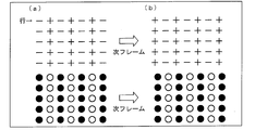
- FIG. 15A in a normally white liquid crystal display device having a high luminance when no drive signal is applied, in the current frame, an intermediate between a black pixel column and white. Tone (that is, gray) pixel columns are alternately displayed. A pixel having a large negative polarity is applied to the pixel indicated by a black circle, while a pixel having a positive polarity sufficient to display a white halftone is applied to the pixel indicated by a white circle.
- the polarity of the display voltage applied to each pixel is inverted by the polarity inversion method. Therefore, a positive display voltage is applied to the pixel indicated by the black circle, while a negative display voltage is applied to the pixel indicated by the white circle to such an extent that a white halftone is displayed. Such polarity inversion is repeated in subsequent frames.
- the display pattern is configured so that the white pixel row that can be visually recognized by one person in one frame has the same polarity in the entire frame, when flicker occurs, the flicker occurs.
- Patent Document 2 listed below discloses a method and apparatus for automatically calculating the optimum voltage Vcom using the flicker value measured by a color analyzer while changing the voltage Vcom of the liquid crystal display device. .
- Patent Documents 1 and 2 have a problem that it is not possible to easily check whether the voltage Vcom is an optimum value without using a special configuration.
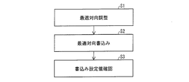
- FIG. 16 shows a general flow relating to a process of setting the voltage Vcom to an optimum value.
- step (abbreviated as S) 1 the voltage Vcom is determined so that flicker does not occur while checking the display screen.
- the display screen for example, as shown in FIG. 17, a confirmation screen I displaying a horizontal stripe still image in which black and gray are alternately arranged for each line, or a display screen as shown in FIG.
- a confirmation screen II displaying a still image of horizontal stripes in which a gradation image changing in 10 steps from black to white and black are alternately arranged for each line from the left end to the right end is suitable.
- the flicker level is determined by judging the flicker level by looking at the state of one screen. Is very difficult to determine. This is because whether or not the flicker is at the minimum level can be determined only by comparing with different screen states in which the value of the voltage Vcom is changed.
- one of the two voltages Vcom is set to the optimum value. Not necessarily. Therefore, the optimum value of the voltage Vcom must be obtained by changing the value of the voltage Vcom in various ways and trial and error.
- Patent Document 2 can automatically calculate the voltage Vcom, there is a problem that a special configuration that enables this is required.
- an object of the present invention is to provide a display inspection method capable of easily confirming whether or not the voltage Vcom is an optimum value without using a special configuration.
- the display inspection method provides (1) While performing inversion driving to invert the polarity of the video signal for each vertical scanning period with respect to the pixel electrode in which the liquid crystal layer is arranged between the counter electrodes, When holding the potential, (2) The counter electrode voltage applied to the counter electrode is a constant voltage, or the center voltage when the polarity of the counter electrode voltage is inverted every vertical scanning period is a constant voltage, (3) The potential difference between the first display area for performing display based on the first video signal in which the center voltage is made equal to the constant voltage of the counter electrode voltage and the adjacent vertical scanning periods is the same as that of the first video signal. On the other hand, at least two display areas including a second display area for performing display based on a second video signal in which the center voltage is different from the constant voltage of the counter electrode voltage are simultaneously displayed on one screen.
- the amplitude of one of the positive and negative polarities (referred to as the first polarity) with reference to the constant voltage of the counter electrode voltage
- the second polarity In a state where the amplitude of the polarity opposite to one polarity (referred to as the second polarity) is equal, display for holding the potential of the video signal is performed during each one vertical scanning period.
- the counter electrode voltage in the first display region is the optimum value, there is no difference in light transmittance in the pixels in each vertical scanning period, so that each pixel displays the same gradation in each vertical scanning period. As a result, no flicker occurs.
- the counter electrode voltage deviates from the optimal value due to human error (optimum value confirmation error) and device error (malfunction) during writing. There is a case. In this case, flicker occurs in the first display area.
- the potential difference between adjacent vertical scanning periods is the same as that of the first video signal, while display based on the second video signal in which the center voltage is different from the constant voltage of the counter electrode voltage.
- the second display area to be performed is displayed in one screen simultaneously with the first display area.
- the second video in which the center voltage of the first video signal is shifted to the first polarity side by ⁇ V.
- a signal can be created.
- the amplitude of the first polarity of the first video signal is reduced by ⁇ V and the amplitude of the second polarity is increased by ⁇ V, the center voltage of the first video signal is shifted to the second polarity side by ⁇ V.
- a second video signal can be created.
- common electrode voltage is commonly applied to all pixels in one screen.
- the present invention by creating the second video signal in which the center voltage of the video signal is different from the constant voltage of the counter electrode voltage, the first display area and the second display area are pseudo-opposed. A state in which the above-mentioned constant voltage of the electrode voltage is changed is created so that two display states can be simultaneously compared on one screen.
- the first video signal in the first display region is set so that the center voltage can be regarded as matching the constant voltage of the counter electrode voltage.
- a combination of a configuration described in a certain claim and a configuration described in another claim is limited to a combination of the configuration described in the claim cited in the claim.
- combinations with configurations described in the claims not cited in the focused claims are possible.
- the counter electrode voltage applied to the counter electrode is set to a constant voltage, or the polarity of the counter electrode voltage is changed every vertical scanning period.
- the potential difference between the first display area that performs display based on the first video signal in which the center voltage when inverted is a constant voltage and the center voltage is matched with the constant voltage of the counter electrode voltage, and the adjacent unit periods is And at least two display areas, which are the same as the first video signal, and a second display area that performs display based on a second video signal in which the center voltage is different from the constant voltage of the counter electrode voltage. Same on screen It is adapted to display in.
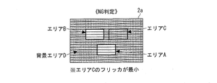
- FIG. 11 is a front view showing a display state in which flicker in area A is minimized in a display inspection process for determining whether or not flicker occurs on the display screen.
- FIG. 11 is a front view showing a display state in which flicker in area B is minimized in a display inspection process for determining whether or not flicker occurs on the display screen.
- FIG. 10 is a front view showing a display state in which flicker in area C is minimized in a display inspection process for determining whether or not flicker occurs on the display screen.
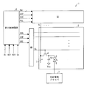
- FIG. 13 is a block diagram showing a configuration of the liquid crystal display device 1, and an equivalent circuit of one pixel 3 is shown in the display unit (liquid crystal panel) 2.
- a configuration related to the counter electrode voltage Vcom hereinafter abbreviated as voltage Vcom
- Vcom the counter electrode voltage
- the pixel 3 is provided corresponding to the intersection of the gate bus line GL and the source bus line SL.
- the pixel 3 normally includes a parasitic capacitor such as a capacitor Cgd formed between the pixel electrode 5 and the gate bus line GL.
- the gate of the TFT 4 is connected to the gate bus line GL, the source of the TFT 4 is connected to the source bus line SL, and the drain of the TFT 4 is connected to the pixel electrode 5.
- the liquid crystal capacitor CL is formed by disposing a liquid crystal layer between the pixel electrode 5 and the counter electrode 6 to which the voltage Vcom is applied.
- the auxiliary capacitor Cs is formed by disposing an insulating film between the pixel electrode 5 or an electrode connected to the pixel electrode 5 and the auxiliary capacitor bus line to which the voltage Vcs is applied.
- the voltage Vcs may be equal to the voltage Vcom, for example, or may be another value.
- the voltage Vcom is manually adjusted by changing the setting of the register constituting the counter electrode driver 7, etc., and the voltage Vcom corresponding to the set value is generated and applied to the counter electrode 6.
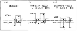
- FIG. 2 is a waveform diagram showing the waveforms of the video signal (source output) applied to the source bus line SL and the voltage Vcom.
- the polarity of the video signal is inverted every frame period (one vertical scanning period) in accordance with the frame inversion driving method.
- the polarity of the voltage Vcom is inverted so as to be opposite to the polarity of the video signal according to the common inversion driving method.
- the amplitude of the video signal can be reduced compared to the case where the voltage Vcom is maintained at a constant value.
- the present invention is also applied to the case where the voltage Vcom is maintained at a constant value without adopting the common inversion driving method.
- the center voltage which is the median value of the positive voltage and the negative voltage of the video signal, coincides with the center voltage of the voltage Vcom (constant voltage described in the claims). It shows the optimum state. That is, the potential difference between the video signal and the voltage Vcom is constant even if the frame changes.
- FIG. 2B shows a state where the center voltage of the voltage Vcom is larger than the center voltage of the video signal
- FIG. 2C shows a state where the center voltage of the voltage Vcom is smaller than the center voltage of the video signal. Show.
- the potential difference between the video signal and the voltage Vcom repeatedly increases and decreases in the frame period, and thus flickers that increase or decrease the light transmittance of the pixels occur.
- the voltage Vcom is applied to all the pixels constituting the display unit 2 with the same value. Therefore, when performing a display inspection to determine whether or not the voltage Vcom is set to an optimum value, conventionally, the entire display screen of the display unit 2 is viewed to check whether flicker has occurred.
- Display driving method in display inspection of the present invention Therefore, in the display inspection method of the present invention, a display region (area shown in FIG. 3) in which the setting of the voltage Vcom is changed in a pseudo manner in a state where the same voltage Vcom is applied to all the pixels constituting the display unit 2.
- A, B, and C) are partially created so that display states before and after the change of the voltage Vcom can be simultaneously confirmed and compared in one screen.
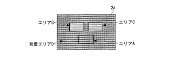
- FIG. 3 is a front view showing a display state of the display screen 2a when performing a display inspection as to whether or not flicker has occurred on the display screen 2a.
- the basic video on the display screen 2a is a horizontal stripe still image in which black and gray are alternately arranged for each line.
- FIG. 1 is a waveform diagram showing the waveform of the source output given to each pixel in areas A to C (corresponding to the first display area, the second display area, and the third display area in this order).
- FIG. 1A shows the waveform of the first video signal applied to the source bus line SL in area A.
- FIG. 1 In the first video signal, the positive voltage corresponding to the gray gradation X is maintained for one frame period, that is, one vertical scanning period, and after the display without gradation change, that is, the still image display, The frame is inverted to a negative voltage by a frame inversion driving method. Even after voltage inversion, display without temporal gradation change is continued.
- the center voltage A (center voltage), which is the median value between the positive voltage and the negative voltage, is considered to be equal to the center voltage of the voltage Vcom as an initial setting.
- background area D background area
- the area A displayed as a partial area in the background area D display based on the first video signal is performed.
- FIG. 1B shows a waveform of a second video signal obtained by correcting the first video signal so as to be applied to the source bus line SL in area B.
- the center voltage B is increased by + ⁇ with respect to the center voltage A while the difference between the positive voltage and the negative voltage of the first video signal is kept constant. That is, the second video signal has a DC component of + ⁇ with respect to the center voltage of the voltage Vcom.
- the display state of the area A and the display state of the area B can be checked at the same time, and the flicker occurrence state can be compared. Therefore, it is determined whether or not the DC setting of the voltage Vcom is appropriate in the area A. It can be easily determined by comparison with the area B.
- FIG. 1 shows the waveform of the third video signal obtained by correcting the first video signal so that the center voltage is shifted in the opposite direction to the second video signal.
- the center voltage C decreases by ⁇ with respect to the center voltage A while the difference between the positive voltage and the negative voltage of the first video signal is kept constant. That is, the third video signal has a DC component of - ⁇ with respect to the center voltage of the voltage Vcom.
- the third video signal is applied to the source bus line SL in area C, which is a partial area of the display screen 2a, display based on the third video signal is performed in area C.
- the display state of area C can be checked simultaneously, and the flicker occurrence state can be compared.
- the polarity of the DC component for correcting the first video signal is reversed. Therefore, by comparing the flickers in the three types of display, the flicker in area A is changed to areas B and C. If it can be confirmed that the flicker is smaller than the flicker, it is possible to make a reliable determination that the flicker in the area A is the smallest.
- the liquid crystal display device includes a source driver having a specification capable of controlling whether the source output is positive or negative with respect to a specific line in a specific field, the flicker of the area A Is not the minimum and the voltage Vcom is not the optimum value, it can be easily determined whether the DC setting of the voltage Vcom should be changed to + or-.
- each of the areas A to C is displayed so as to be surrounded by the background area D that performs display based on the first video signal, it is possible to check the flicker variation in one screen.
- the flicker variation in one screen is caused by a parasitic capacitance variation of a thin film transistor or the like in the screen, a cell thickness variation, a cause due to contamination of the screen periphery (seal material periphery), and the like.
- the counter electrode driver 7 includes a type in which the set value of the voltage Vcom can be written only once and a type in which the set value can be written twice or more depending on specifications. If the comparison between the areas A to C confirms that the flicker in the area A is not minimum, the counter electrode driver 7 of the type that can write the setting value twice or more rewrites the setting value, The display inspection process can be repeated to find the optimum value of the voltage Vcom.
- the positive voltage (positive source output) and negative voltage (negative source output) of the output video signal corresponding to each gradation of the input data signal that is the basis of the video signal ) Is decided. That is, if the gradation is different, the source output is also different.
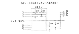
- FIG. 4 is a waveform diagram conceptually showing the waveform of the source output in the n field (n frame) for the pixels of the m line
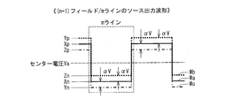
- FIG. 5 is the waveform of the source output in the (n + 1) field for the same pixel of the m line. It is a wave form diagram which shows a waveform notionally.
- FIGS. 6 and 7 are front views showing display states of areas A to C in the n field and (n + 1) field, respectively.
- the display of the areas A to C is created by using three combinations of gradations X, Y, and Z having different source outputs.
- the positive polarity source outputs (V) of the gradations X, Y, and Z are Xp, Yp, and Zp, respectively, and the negative polarity source outputs (V) are Xn, Yn, and Zn, respectively.
- the gradation Y is a gradation in which the positive polarity source output Yp is (Xp + ⁇ ) V and the negative polarity source output Yn is (Xn ⁇ ) V.
- the gradation Z is a gradation in which the positive polarity source output Zp is (Xp ⁇ ) V and the negative polarity source output Zn is (Xn + ⁇ ) V.
- the display screen 2 a when performing the display inspection has an arbitrary gradation other than black and black (for example, 128 gradations in the case of an 8-bit input data signal).
- An image in which flicker is easy to check is displayed, such as a horizontal stripe still image alternately arranged for each line.
- a gradation image that changes from black to white in 10 steps may be displayed from the left end to the right end of the display screen.
- the arbitrary gradation is X gradation in the n field, and X gradation is also in the (n + 1) field, and the source output is the positive source output Xp in the n field.
- the negative polarity source output Xn is used in the (n + 1) field. That is, the waveform of the source output (first video signal) for the pixels in area A is the waveform Wa shown in FIGS.
- the above-mentioned arbitrary gradation is Y gradation in the n field, Z gradation in the (n + 1) field, and the source output is positive source output Yp in the n field and negative polarity in the (n + 1) field.
- the source output is Zn. That is, the waveform of the source output (second video signal) for the pixels in area B is the waveform Wb shown in FIGS.
- the arbitrary gradation is Z gradation in the n field
- the source output is the positive source output Zp in the n field
- the second video signal and the third video signal are created by correcting the input gradation data supplied to the source driver SD (FIG. 13) that outputs the first video signal.
- the second video signal and the third video signal are the input gradation data corresponding to the positive voltage of the first video signal and the input corresponding to the negative voltage of the first video signal, respectively. It is created by correcting gradation data. Then, the input gradation data is corrected so that the positive voltage and the negative voltage of the first video signal are shifted to the same polarity side with the same correction amount ( ⁇ ). As a result, the shift amounts of the center voltages of the second video signal and the third video signal are also equal to the correction amount ( ⁇ ), so that the display in which the DC setting of the voltage Vcom is changed in a pseudo manner can be easily performed. Can do.
- the input gradation is changed from gradation Y to gradation Z in area B, while the input gradation is changed from gradation Z to gradation Y in area C.
- the flicker of area A can be reduced by simply switching the input gradation between area B and area C. If it is minimum, it can be determined that it is optimal.
- the center voltage of area B is shifted to either + ⁇ or ⁇ , regardless of the specifications of the source driver, and the center voltage of area C is + ⁇ or ⁇ . It is possible to shift to the other of the two.
- FIG. 8 is an explanatory diagram showing how to set the input data signal in each area when the allowable range of the optimum setting value of the voltage Vcom at which flicker is minimized is managed as ⁇ 1 bit
- FIG. 9 is a diagram in which flicker is minimized. It is explanatory drawing which shows the setting method of the input data signal of each area in the case of managing the tolerance
- the n field and the (n + 1) field have predetermined gradations (for example, 128 gradations).
- the data corresponding to the halftone) is input to the source driver SD (FIG. 13).
- ⁇ is a value corresponding to ⁇ 3 bits as a DC adjustment of the voltage Vcom.
- the gradation of the input data signal is determined so that the above-described deviation in the source output center voltage increase / decrease amount occurs in either the center voltage B or the center voltage C of the source output.
- the polarity of the input data signal is reversed, and a deviation of + ⁇ corresponding to +3 bits as the DC adjustment of the voltage Vcom becomes the center voltage B or the center voltage C of the source output.
- the gradation of the input data signal is determined so as to occur.
- the determination of the gradation of the input data signal as described above is based on the use of a source driver that cannot control the polarity of the input data signal.
- the correct DC setting of the voltage Vcom written to the counter electrode driver 7 is in the positive direction of +2 bits or more as shown in FIG. 8, the other flicker of the area B or the area C is minimized.
- the allowable range is managed as ⁇ 2 bits as shown in FIG. 9, for example, for either one of the areas B and C, the deviation of ⁇ corresponding to ⁇ 5 bits as the DC adjustment of the voltage Vcom is The gradation of the input data signal is determined so as to occur at either the center voltage B or the center voltage C of the source output.
- the polarity of the input data signal is reversed, and a deviation of + ⁇ corresponding to +5 bits as the DC adjustment amount of the voltage Vcom is changed to the center voltage B or the center voltage C of the source output.
- the gradation of the input data signal is determined so as to occur.
- FIG. 10 is a front view showing a display state in which the flicker in area A is minimized in the display inspection process for checking whether or not flicker has occurred
- FIG. 11 is a display state in which the flicker in area B is minimized
- FIG. 12 is a front view showing a display state in which the flicker in area C is minimized.
- FIG. 10 shows a state where the flicker in area A is minimized as a result of the correct DC setting of the voltage Vcom written to the counter electrode driver 7.
- FIG. 11 shows that, for example, a shift of ⁇ corresponding to ⁇ 3 bits or a shift of + ⁇ corresponding to +3 bits occurs in the center voltage B of the source output, and as a result, the flicker in area B is minimized. Represents a state.
- FIG. 12 shows that, for example, a shift of ⁇ corresponding to ⁇ 3 bits or a shift of + ⁇ corresponding to +3 bits occurs in the center voltage C of the source output, and as a result, the flicker in area C is minimized. Represents a state.
- the normal input display area in which the center voltage of the voltage Vcom and the center voltage of the source output are matched with each other and the center voltage are intentionally shifted. Since the display area is displayed, it can be easily confirmed visually whether or not the DC setting value of the voltage Vcom written to the counter electrode driver 7 is optimal.
- each of the areas A to C is displayed so as to be surrounded by the background area D on one screen, and the background area D is displayed based on the same source output as the area A. Thereby, it is possible to check the flicker variation in one screen.
- An input data signal corresponding to the output may be generated.
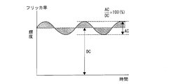
- the flicker rate is a ratio between the luminance fluctuation width AC of the display screen and the average luminance value DC expressed as a percentage, that is, (AC / DC) ⁇ 100.
- the liquid crystal display device 1 includes a source driver SD, a gate driver GD, and a display control circuit 8 in addition to the display unit 2.
- the source driver SD drives the source bus line SL
- the gate driver GD drives the gate bus line GL
- the display control circuit 8 controls the source driver SD and the gate driver GD.
- a storage capacitor wiring driving circuit for driving the storage capacitor wiring (Cs wiring) may be provided as necessary.
- the display control circuit 8 performs a display operation from an external signal source (for example, a tuner), a digital video signal Dv representing an image to be displayed, a horizontal synchronization signal HSY and a vertical synchronization signal VSY corresponding to the digital video signal Dv.
- an external signal source for example, a tuner
- Dv digital video signal
- HSY horizontal synchronization signal
- VSY vertical synchronization signal
- the display control circuit 8 uses the data start pulse signal SSP and the data as signals for causing the display unit to display an image represented by the digital video signal Dv based on the received signals Dv, HSY, VSY, and Dc.
- the digital video signal Dv is output from the display control circuit 8 as a digital image signal DA after timing adjustment or the like is performed as necessary in the internal memory.
- the data clock signal SCK is generated as a signal composed of pulses corresponding to each pixel of the image represented by the digital image signal DA.
- the data start pulse signal SSP is generated as a signal that becomes high level (H level) for a predetermined period every horizontal scanning period based on the horizontal synchronization signal HSY.
- the gate start pulse signal GSP is generated as a signal that becomes H level for a predetermined period every frame period (one vertical scanning period) based on the vertical synchronization signal VSY.
- the gate clock signal GCK is generated based on the horizontal synchronization signal HSY.
- the gate driver output control signal GOE is generated based on the horizontal synchronization signal HSY and the control signal Dc.
- the polarity inversion signal POL, the data start pulse signal SSP, and the data clock signal SCK for controlling the polarity of the digital image signal DA are input to the source driver SD.
- the gate start pulse signal GSP, the gate clock signal GCK, and the gate driver output control signal GOE are input to the gate driver GD.
- the source driver SD is based on the digital image signal DA, the data clock signal SCK, the data start pulse signal SSP, and the polarity inversion signal POL, and an analog potential (corresponding to the pixel value in each scanning signal line of the image represented by the digital image signal DA). Data signals) are sequentially generated every horizontal scanning period, and these data signals are output to the source bus line SL.
- the gate driver GD generates a gate-on pulse signal based on the gate start pulse signal GSP, the gate clock signal GCK, and the gate driver output control signal GOE, and outputs them to the gate bus line GL.
- GL is selectively driven.
- the gate bus line GL and the source bus line SL of the display unit 2 are driven by the source driver SD and the gate driver GD, so that the source is connected via the TFT 4 connected to the selected gate bus line GL.
- a data signal is written from the bus line SL to the pixel electrode 5.
- a voltage is applied to the liquid crystal layer of each pixel 3, whereby the transmittance of light from the backlight is controlled, and an image indicated by the digital video signal Dv is displayed.
- the display inspection method further includes a display based on a third video signal in which the center voltage is different from the center voltage of the second video signal on the opposite polarity side with respect to the constant voltage of the counter electrode voltage.
- the third display area to be performed is simultaneously displayed on the one screen.
- the three states in which the constant voltage of the counter electrode voltage is pseudo-shifted to both positive and negative polarities on the basis of the constant voltage of the counter electrode voltage in the first display area are simultaneously confirmed on one screen. can do.
- a reliable determination can be made that the flicker in the first display area is minimum.
- the liquid crystal display device includes a source driver having a specification capable of controlling whether the source output is positive or negative with respect to a specific line in a specific field, the first display region When the flicker is not the minimum and the counter electrode voltage is not the optimum value, it can be easily determined whether the counter electrode voltage should be increased or decreased.
- the display inspection method further displays each of the display areas so as to be surrounded by the background area on the one screen, and performs display based on the first video signal in the background area. It is characterized by.
- the flicker of one screen can be reduced. Variations can be confirmed.
- the flicker variation in one screen is caused by a parasitic capacitance variation of a thin film transistor or the like in the screen, a cell thickness variation, a cause due to contamination of the screen periphery (seal material periphery), and the like.
- the center voltage is set according to the shift amount that is expected to occur in the counter electrode voltage under the influence of a factor including at least one of temperature change, change with time, and light irradiation.
- the display is performed in the second display area or the third display area, and is generated in the second display area or the third display area. It is characterized in that it is determined whether or not the flicker exceeds an allowable level.
- the flicker generated in the second display area is determined whether it exceeds the allowable level by measuring the flicker rate using a measuring device or the limit arranged so that the flicker rate becomes the maximum value of the allowable level. There are methods such as comparison with samples.
- the present invention can be used for a display inspection method in an AC drive type liquid crystal display device.
Landscapes
- Engineering & Computer Science (AREA)
- Chemical & Material Sciences (AREA)
- Crystallography & Structural Chemistry (AREA)
- Physics & Mathematics (AREA)
- Computer Hardware Design (AREA)
- General Physics & Mathematics (AREA)
- Theoretical Computer Science (AREA)
- Liquid Crystal Display Device Control (AREA)
- Control Of Indicators Other Than Cathode Ray Tubes (AREA)
- Liquid Crystal (AREA)
- Testing, Inspecting, Measuring Of Stereoscopic Televisions And Televisions (AREA)
Abstract
Description
(1)対向電極との間に液晶層を配置した画素電極に対して、1垂直走査期間毎に映像信号の極性を反転させる反転駆動を行いながら、各1垂直走査期間中は上記映像信号の電位を保持するときに、
(2)上記対向電極に印加する対向電極電圧を一定電圧とするか、あるいは、1垂直走査期間毎に対向電極電圧の極性を反転させた場合の中心電圧を一定電圧とし、
(3)中心電圧を上記対向電極電圧の上記一定電圧に一致させた第1映像信号に基づく表示を行う第1表示領域と、隣り合う垂直走査期間同士の電位差は、上記第1映像信号と同じである一方、中心電圧を上記対向電極電圧の上記一定電圧と異ならせた第2映像信号に基づく表示を行う第2表示領域との少なくとも2つの表示領域を、1画面上に同時に表示すること
を特徴とする。
図13は、液晶表示装置1の構成を示すブロック図であり、表示部(液晶パネル)2には、1つの画素3の等価回路が示されている。ここでは、対向電極電圧Vcom(以下、電圧Vcomと略称する)に関わる構成について説明し、それ以外の構成については、後述する。
図2は、ソースバスラインSLに印加される映像信号(ソース出力)および電圧Vcomの波形を示す波形図である。映像信号の極性は、フレーム反転駆動方式に従って、1フレーム期間(1垂直走査期間)毎に反転している。
そこで、本発明の表示検査方法では、表示部2を構成する全ての画素に共通して同じ電圧Vcomを印加した状態で、擬似的に電圧Vcomの設定を変えた表示領域(図3に示すエリアA、B,C)を部分的に作り、電圧Vcomの変更前後の表示状態を1画面内で同時に確認して、比較できるようにしている。
以下、第2映像信号および第3映像信号の電圧設定について、さらに詳細に説明する。
エリアB:Yp-Zn=((Xp+α)-(Xn+α))=Xp-Xn=Vpp 式2
エリアC:Zp-Yn=((Xp-α)-(Xn-α))=Xp-Xn=Vpp 式3
また、エリアAのソース出力のセンター電圧AをVaとすると、エリアBのセンター電圧は、Va+α、エリアCのセンター電圧は、Va-αとなり、通常入力のエリアAに対して、エリアBおよびエリアCのセンター電圧を+αまたは-αずらすことが可能になる。
次に、図8および図9を参照して、上記エリアA~Cの表示を実現するための入力データ信号の階調設定について説明する。
以上の設定に基づいて、エリアA~Cに表示を行い、フリッカの発生状態を検査する。図10は、フリッカが発生しているかどうかの表示検査工程において、エリアAのフリッカが最小になっている表示状態を示す正面図、図11は、エリアBのフリッカが最小になっている表示状態を示す正面図、図12は、エリアCのフリッカが最小になっている表示状態を示す正面図である。
最後に、図13に戻って、液晶表示装置1のその他の構成と動作とについて、触れておく。
6 対向電極
5 画素電極
Wa 波形(第1映像信号)
Wb 波形(第2映像信号)
Wc 波形(第3映像信号)
Claims (8)
- 対向電極との間に液晶層を配置した画素電極に対して、1垂直走査期間毎に映像信号の極性を反転させる反転駆動を行いながら、各1垂直走査期間中は上記映像信号の電位を保持するときに、
上記対向電極に印加する対向電極電圧を一定電圧とするか、あるいは、1垂直走査期間毎に対向電極電圧の極性を反転させた場合の中心電圧を一定電圧とし、
中心電圧を上記対向電極電圧の上記一定電圧に一致させた第1映像信号に基づく表示を行う第1表示領域と、隣り合う垂直走査期間同士の電位差は、上記第1映像信号と同じである一方、中心電圧を上記対向電極電圧の上記一定電圧と異ならせた第2映像信号に基づく表示を行う第2表示領域との少なくとも2つの表示領域を、1画面上に同時に表示すること
を特徴とする表示検査方法。 - 上記対向電極電圧の上記一定電圧に対し、中心電圧を上記第2映像信号の上記中心電圧と逆極性側に異ならせた第3映像信号に基づく表示を行う第3表示領域を、上記1画面上に同時に表示すること
を特徴とする請求項1に記載の表示検査方法。 - 上記表示領域のそれぞれを、上記1画面上の背景領域に囲まれるように表示し、
上記背景領域には、上記第1映像信号に基づく表示を行うことを特徴とする請求項1または2に記載の表示検査方法。 - 温度変化、経時変化および光照射の少なくとも1つを含む要因の影響を受けて、上記対向電極電圧に発生すると予測されるシフト量に応じて、中心電圧を上記対向電極電圧の上記一定電圧と異ならせた第2映像信号または第3映像信号に基づき、第2表示領域または第3表示領域に表示を行い、
当該第2表示領域または第3表示領域に発生するフリッカが、許容レベルを超えているかどうかを判定すること
を特徴とする請求項2に記載の表示検査方法。 - 上記第2映像信号は、上記第1映像信号を出力するソースドライバに与える入力階調のデータを補正することによって作成されること
を特徴とする請求項1に記載の表示検査方法。 - 上記第2映像信号は、上記第1映像信号の正極性電圧に対応する上記入力階調のデータと、上記第1映像信号の負極性電圧に対応する上記入力階調のデータとをそれぞれを補正することによって作成されること
を特徴とする請求項5に記載の表示検査方法。 - 上記第3映像信号は、上記第1映像信号を出力するソースドライバに与える入力階調のデータを補正することによって作成されること
を特徴とする請求項2に記載の表示検査方法。 - 上記第3映像信号は、上記第1映像信号の正極性電圧に対応する上記入力階調のデータと、上記第1映像信号の負極性電圧に対応する上記入力階調のデータとをそれぞれを補正することによって作成されること
を特徴とする請求項7に記載の表示検査方法。
Priority Applications (2)
| Application Number | Priority Date | Filing Date | Title |
|---|---|---|---|
| CN201180009554.2A CN102763157B (zh) | 2010-02-17 | 2011-02-15 | 显示检查方法 |
| JP2012500602A JP5512788B2 (ja) | 2010-02-17 | 2011-02-15 | 液晶表示装置の表示検査方法 |
Applications Claiming Priority (2)
| Application Number | Priority Date | Filing Date | Title |
|---|---|---|---|
| JP2010032406 | 2010-02-17 | ||
| JP2010-032406 | 2010-02-17 |
Publications (1)
| Publication Number | Publication Date |
|---|---|
| WO2011102347A1 true WO2011102347A1 (ja) | 2011-08-25 |
Family
ID=44482932
Family Applications (1)
| Application Number | Title | Priority Date | Filing Date |
|---|---|---|---|
| PCT/JP2011/053164 Ceased WO2011102347A1 (ja) | 2010-02-17 | 2011-02-15 | 表示検査方法 |
Country Status (3)
| Country | Link |
|---|---|
| JP (1) | JP5512788B2 (ja) |
| CN (1) | CN102763157B (ja) |
| WO (1) | WO2011102347A1 (ja) |
Families Citing this family (1)
| Publication number | Priority date | Publication date | Assignee | Title |
|---|---|---|---|---|
| CN108682401B (zh) * | 2018-03-19 | 2021-05-18 | Oppo广东移动通信有限公司 | 液晶显示屏公共电压控制方法、电路、设备及介质 |
Citations (4)
| Publication number | Priority date | Publication date | Assignee | Title |
|---|---|---|---|---|
| JPH1062748A (ja) * | 1996-06-07 | 1998-03-06 | Toshiba Corp | アクティブマトリクス型表示装置の調整方法 |
| JP2003122316A (ja) * | 2001-10-17 | 2003-04-25 | Matsushita Electric Ind Co Ltd | 交流駆動型マトリックス表示装置およびフリッカー調整方法 |
| JP2007156247A (ja) * | 2005-12-07 | 2007-06-21 | Sharp Corp | 表示装置の製造方法 |
| JP2009163090A (ja) * | 2008-01-09 | 2009-07-23 | Mitsubishi Electric Corp | 液晶パネル検査方法 |
Family Cites Families (2)
| Publication number | Priority date | Publication date | Assignee | Title |
|---|---|---|---|---|
| JP4330059B2 (ja) * | 2000-11-10 | 2009-09-09 | カシオ計算機株式会社 | 液晶表示装置及びその駆動制御方法 |
| JP4127249B2 (ja) * | 2003-11-27 | 2008-07-30 | セイコーエプソン株式会社 | 電気光学装置の調整方法、電気光学装置の調整装置および電子機器 |
-
2011
- 2011-02-15 WO PCT/JP2011/053164 patent/WO2011102347A1/ja not_active Ceased
- 2011-02-15 CN CN201180009554.2A patent/CN102763157B/zh not_active Expired - Fee Related
- 2011-02-15 JP JP2012500602A patent/JP5512788B2/ja active Active
Patent Citations (4)
| Publication number | Priority date | Publication date | Assignee | Title |
|---|---|---|---|---|
| JPH1062748A (ja) * | 1996-06-07 | 1998-03-06 | Toshiba Corp | アクティブマトリクス型表示装置の調整方法 |
| JP2003122316A (ja) * | 2001-10-17 | 2003-04-25 | Matsushita Electric Ind Co Ltd | 交流駆動型マトリックス表示装置およびフリッカー調整方法 |
| JP2007156247A (ja) * | 2005-12-07 | 2007-06-21 | Sharp Corp | 表示装置の製造方法 |
| JP2009163090A (ja) * | 2008-01-09 | 2009-07-23 | Mitsubishi Electric Corp | 液晶パネル検査方法 |
Also Published As
| Publication number | Publication date |
|---|---|
| JP5512788B2 (ja) | 2014-06-04 |
| CN102763157B (zh) | 2015-01-14 |
| JPWO2011102347A1 (ja) | 2013-06-17 |
| CN102763157A (zh) | 2012-10-31 |
Similar Documents
| Publication | Publication Date | Title |
|---|---|---|
| KR100615016B1 (ko) | 액정표시장치 | |
| US8049698B2 (en) | Liquid crystal display and driving method thereof | |
| CN102842299B (zh) | 一种液晶显示装置的驱动方法、驱动装置及液晶显示装置 | |
| US8525540B2 (en) | Switch control unit, test apparatus and method for liquid crystal cell | |
| JP2011053693A (ja) | フリッカが低減された液晶表示装置及びフリッカ低減方法 | |
| CN101101421A (zh) | 液晶显示设备和液晶显示设备的驱动方法 | |
| US20190325830A1 (en) | Display control method and apparatus, computer readable storage medium, and computer device | |
| CN100583222C (zh) | 共用电压补偿装置、液晶显示器及其驱动方法 | |
| KR20130110388A (ko) | 액정표시장치의 플리커 조정방법 | |
| KR101992885B1 (ko) | 액정 표시장치의 구동장치와 그 구동방법 | |
| CN109844851B (zh) | 液晶显示装置的亮度不均修正方法以及修正数据生成装置 | |
| CN100358000C (zh) | 矩阵显示器件 | |
| US7212180B2 (en) | Method of driving liquid crystal display device | |
| KR20070062836A (ko) | 액정표시장치의 잔상 방지회로 및 그 방법 | |
| CN113129849B (zh) | 像素驱动电路及像素驱动方法 | |
| JP5512788B2 (ja) | 液晶表示装置の表示検査方法 | |
| KR101493526B1 (ko) | 액정표시장치 | |
| KR20080054658A (ko) | 액정 표시장치의 구동장치와 그 구동방법 | |
| WO2014007199A1 (ja) | 液晶表示装置およびその制御方法、ならびにゲートドライバ | |
| KR102132226B1 (ko) | 액정표시장치 및 이의 구동방법 | |
| KR101992880B1 (ko) | 액정 표시장치 | |
| CN113362780A (zh) | 显示面板及其显示控制方法、显示装置 | |
| KR20110071538A (ko) | 액정 표시장치의 구동장치와 그 구동방법 | |
| KR100864980B1 (ko) | 액정표시장치의 잔상방지장치 | |
| KR100934826B1 (ko) | 액정 표시소자의 감마 기준전압 설정방법 |
Legal Events
| Date | Code | Title | Description |
|---|---|---|---|
| WWE | Wipo information: entry into national phase |
Ref document number: 201180009554.2 Country of ref document: CN |
|
| 121 | Ep: the epo has been informed by wipo that ep was designated in this application |
Ref document number: 11744633 Country of ref document: EP Kind code of ref document: A1 |
|
| WWE | Wipo information: entry into national phase |
Ref document number: 2012500602 Country of ref document: JP |
|
| NENP | Non-entry into the national phase |
Ref country code: DE |
|
| 122 | Ep: pct application non-entry in european phase |
Ref document number: 11744633 Country of ref document: EP Kind code of ref document: A1 |