WO2011102338A1 - 保護監視回路、及び電池パック - Google Patents
保護監視回路、及び電池パック Download PDFInfo
- Publication number
- WO2011102338A1 WO2011102338A1 PCT/JP2011/053128 JP2011053128W WO2011102338A1 WO 2011102338 A1 WO2011102338 A1 WO 2011102338A1 JP 2011053128 W JP2011053128 W JP 2011053128W WO 2011102338 A1 WO2011102338 A1 WO 2011102338A1
- Authority
- WO
- WIPO (PCT)
- Prior art keywords
- secondary battery
- voltage
- protection
- circuit
- monitoring circuit
- Prior art date
- Legal status (The legal status is an assumption and is not a legal conclusion. Google has not performed a legal analysis and makes no representation as to the accuracy of the status listed.)
- Ceased
Links
Images



Classifications
-
- H—ELECTRICITY
- H01—ELECTRIC ELEMENTS
- H01M—PROCESSES OR MEANS, e.g. BATTERIES, FOR THE DIRECT CONVERSION OF CHEMICAL ENERGY INTO ELECTRICAL ENERGY
- H01M10/00—Secondary cells; Manufacture thereof
- H01M10/42—Methods or arrangements for servicing or maintenance of secondary cells or secondary half-cells
- H01M10/48—Accumulators combined with arrangements for measuring, testing or indicating the condition of cells, e.g. the level or density of the electrolyte
-
- H—ELECTRICITY
- H02—GENERATION; CONVERSION OR DISTRIBUTION OF ELECTRIC POWER
- H02H—EMERGENCY PROTECTIVE CIRCUIT ARRANGEMENTS
- H02H7/00—Emergency protective circuit arrangements specially adapted for specific types of electric machines or apparatus or for sectionalised protection of cable or line systems, and effecting automatic switching in the event of an undesired change from normal working conditions
- H02H7/18—Emergency protective circuit arrangements specially adapted for specific types of electric machines or apparatus or for sectionalised protection of cable or line systems, and effecting automatic switching in the event of an undesired change from normal working conditions for batteries; for accumulators
-
- H—ELECTRICITY
- H02—GENERATION; CONVERSION OR DISTRIBUTION OF ELECTRIC POWER
- H02J—ELECTRIC POWER NETWORKS; CIRCUIT ARRANGEMENTS OR SYSTEMS FOR SUPPLYING OR DISTRIBUTING ELECTRIC POWER; SYSTEMS FOR STORING ELECTRIC ENERGY
- H02J7/00—Circuit arrangements for charging or discharging batteries or for supplying loads from batteries
- H02J7/60—Circuit arrangements for charging or discharging batteries or for supplying loads from batteries including safety or protection arrangements
- H02J7/663—Circuit arrangements for charging or discharging batteries or for supplying loads from batteries including safety or protection arrangements using battery or load disconnect circuits
-
- H—ELECTRICITY
- H01—ELECTRIC ELEMENTS
- H01M—PROCESSES OR MEANS, e.g. BATTERIES, FOR THE DIRECT CONVERSION OF CHEMICAL ENERGY INTO ELECTRICAL ENERGY
- H01M10/00—Secondary cells; Manufacture thereof
- H01M10/05—Accumulators with non-aqueous electrolyte
- H01M10/052—Li-accumulators
-
- H—ELECTRICITY
- H02—GENERATION; CONVERSION OR DISTRIBUTION OF ELECTRIC POWER
- H02J—ELECTRIC POWER NETWORKS; CIRCUIT ARRANGEMENTS OR SYSTEMS FOR SUPPLYING OR DISTRIBUTING ELECTRIC POWER; SYSTEMS FOR STORING ELECTRIC ENERGY
- H02J7/00—Circuit arrangements for charging or discharging batteries or for supplying loads from batteries
- H02J7/60—Circuit arrangements for charging or discharging batteries or for supplying loads from batteries including safety or protection arrangements
- H02J7/61—Circuit arrangements for charging or discharging batteries or for supplying loads from batteries including safety or protection arrangements against overcharge
-
- H—ELECTRICITY
- H02—GENERATION; CONVERSION OR DISTRIBUTION OF ELECTRIC POWER
- H02J—ELECTRIC POWER NETWORKS; CIRCUIT ARRANGEMENTS OR SYSTEMS FOR SUPPLYING OR DISTRIBUTING ELECTRIC POWER; SYSTEMS FOR STORING ELECTRIC ENERGY
- H02J7/00—Circuit arrangements for charging or discharging batteries or for supplying loads from batteries
- H02J7/60—Circuit arrangements for charging or discharging batteries or for supplying loads from batteries including safety or protection arrangements
- H02J7/62—Circuit arrangements for charging or discharging batteries or for supplying loads from batteries including safety or protection arrangements against overcurrent
-
- H—ELECTRICITY
- H02—GENERATION; CONVERSION OR DISTRIBUTION OF ELECTRIC POWER
- H02J—ELECTRIC POWER NETWORKS; CIRCUIT ARRANGEMENTS OR SYSTEMS FOR SUPPLYING OR DISTRIBUTING ELECTRIC POWER; SYSTEMS FOR STORING ELECTRIC ENERGY
- H02J7/00—Circuit arrangements for charging or discharging batteries or for supplying loads from batteries
- H02J7/60—Circuit arrangements for charging or discharging batteries or for supplying loads from batteries including safety or protection arrangements
- H02J7/63—Circuit arrangements for charging or discharging batteries or for supplying loads from batteries including safety or protection arrangements against overdischarge
-
- Y—GENERAL TAGGING OF NEW TECHNOLOGICAL DEVELOPMENTS; GENERAL TAGGING OF CROSS-SECTIONAL TECHNOLOGIES SPANNING OVER SEVERAL SECTIONS OF THE IPC; TECHNICAL SUBJECTS COVERED BY FORMER USPC CROSS-REFERENCE ART COLLECTIONS [XRACs] AND DIGESTS
- Y02—TECHNOLOGIES OR APPLICATIONS FOR MITIGATION OR ADAPTATION AGAINST CLIMATE CHANGE
- Y02E—REDUCTION OF GREENHOUSE GAS [GHG] EMISSIONS, RELATED TO ENERGY GENERATION, TRANSMISSION OR DISTRIBUTION
- Y02E60/00—Enabling technologies; Technologies with a potential or indirect contribution to GHG emissions mitigation
- Y02E60/10—Energy storage using batteries
Definitions
- the present disclosure relates to a protection monitoring circuit and a battery pack including the protection monitoring circuit.
- Lithium ion batteries as rechargeable secondary batteries have been installed in portable devices such as digital cameras and mobile phones.
- Lithium ion batteries are generally vulnerable to overcharge, overcurrent, overdischarge, etc., and are in the form of a battery pack with a protection circuit that protects the lithium ion battery by detecting overcharge, overcurrent, overdischarge, etc. Used in.
- Such a battery pack may be equipped with a secondary battery monitoring circuit or the like that detects a state such as a remaining battery level of the lithium ion battery.
- the voltage that can be input to the secondary battery monitoring circuit decreases due to a decrease in breakdown voltage accompanying the miniaturization. . In this case, it may be difficult to directly input the battery voltage of the secondary battery to the secondary battery monitoring circuit.
- the secondary battery monitoring circuit includes a voltage sensor that detects the battery voltage of the secondary battery.
- ESD electrostatic discharge
- the protection monitoring circuit detects at least one of overcharge, overdischarge, and overcurrent of a rechargeable secondary battery, and performs on / off control of the control transistor to control the second.
- the battery pack includes a secondary battery and a protection monitoring circuit
- the protection monitoring circuit is at least one of overcharge, overdischarge, and overcurrent of the rechargeable secondary battery.
- a protection circuit that protects the secondary battery by controlling on / off of the control transistor, and a fine voltage that has a withstand voltage lower than the battery voltage of the secondary battery and detects the state of the secondary battery
- the secondary battery monitoring circuit, and the protection circuit generates a voltage within a withstand voltage range of the secondary battery monitoring circuit according to the output voltage of the secondary battery, the secondary battery monitoring circuit A detection value corresponding to the generated voltage supplied from the protection circuit is generated, and the detection value indicates an output voltage of the secondary battery.
- the secondary battery monitoring circuit can detect the output voltage of the secondary battery even when the withstand voltage is reduced due to the miniaturization of the circuit, and the electrostatic resistance is further improved. Can be made.
- FIG. 1 is a diagram illustrating an example of a circuit diagram of a related art battery pack.
- the battery pack 100 includes a protection monitoring circuit 101, a rechargeable secondary battery 110 such as a lithium ion battery, a secondary battery connection positive terminal 112, a secondary battery negative terminal 113, an external A positive terminal 114 as a terminal and a negative terminal 115 are included.
- the battery pack 100 is used by being connected to a portable device, a charging device or the like via a positive electrode terminal 114 and a negative electrode terminal 115.
- the protection monitoring circuit 101 and the secondary battery 110 are connected by a secondary battery connection positive terminal 112 and a secondary battery negative terminal 113.
- the protection monitoring circuit 101 includes a protection IC (Integrated Circuit) 120 and a secondary battery monitoring IC 130.
- the protection monitoring circuit 101 includes resistors R1 to R5, capacitors C1 to C4, and parasitics.
- a MOS (Metal Oxide Semiconductor) transistor M11 having a diode D1, a MOS transistor M12 having a parasitic diode D2, a positive terminal 114, a negative terminal 115, and an external terminal 116 are included.
- the protection monitoring circuit 101 is configured as a protection module or COB (Chip on Board) by arranging these components on the same substrate.
- the protection IC 120 incorporates an overcharge detection circuit, an overdischarge detection circuit, an overcurrent detection circuit, and the like, and detects overcharge, overcurrent, overdischarge, etc. of the secondary battery 110, and is connected to a portable device or the like or a charging device.
- the control transistor provided between the secondary battery 110 is turned on / off.
- the protection IC 120 is connected to the power supply terminal VDD1, the reference potential terminal VSS1, the power supply voltage supply terminal VREGOUT, the voltage detection terminal VSENSE, the communication terminals SIOI and SIOE, and the negative terminal 115. V ⁇ , DOUT terminal, and COUT terminal.
- the protection IC 120 is supplied with a power supply voltage from VDD 1 connected to the positive electrode of the secondary battery 110.
- the protection IC 120 regulates the supplied power supply voltage, outputs the regulated power supply voltage from VREGOUT to VDD2 of the secondary battery monitoring IC 130, and supplies the power supply voltage to the secondary battery monitoring IC 130.
- the protection IC 120 detects the voltage of the secondary battery 110 by VSENSE connected to the positive electrode of the secondary battery 110, and detects, for example, overcharge, overdischarge, and the like.
- the protection IC 120 outputs control signals for controlling the MOS transistors M11 and M12 to the DOUT terminal and the COUT terminal respectively connected to the gates of the MOS transistors M11 and M12 that cut off charging / discharging of the battery pack 100.
- the protection IC 120 When the protection IC 120 detects, for example, overdischarge, discharge overcurrent, or the like, the output of the DOUT terminal is set to the low level to shut off (turn off) the MOS transistor M11. Further, when the overcharge and the overcharge current are detected, the protection IC 120 sets the output of the COUT terminal to a low level and shuts off (turns off) the MOS transistor M12.
- the protection IC 120 allows communication information between the secondary battery monitoring IC 130 and the portable device or the like to pass from the SIOE or SIOI connected to the communication terminal 116 that performs communication with the portable device or the like.
- the secondary battery monitoring IC 130 detects the output voltage and the like of the secondary battery 110 and detects the state of the secondary battery 110 such as the remaining battery level.
- the secondary battery monitoring IC 130 has a power supply terminal VDD2, a voltage detection terminal VBAT, a reference potential terminal VSS2, a pair of voltage detection terminals VRSP and VRSM, and a communication terminal SIO. Configured.
- the secondary battery monitoring IC 130 is supplied with a power supply voltage from VDD 2 connected to VREGOUT of the protection IC 120. Further, the secondary battery monitoring IC 130 detects the voltage flowing across the resistor R3 by detecting the voltage at both ends of the resistor R3 outside the secondary battery monitoring IC 130 using the VRSM terminal and the VRSP terminal which are voltage detection terminals. Thus, the charge / discharge current of the secondary battery 110 is detected. In addition, the secondary battery monitoring IC 130 performs communication with the mobile device or the like from the communication terminal 116 of the mobile device or the like and the SIO connected via the protection IC 120.
- the secondary battery monitoring IC 130 detects by directly inputting the output voltage of the secondary battery 110 by VBAT connected to the positive electrode of the secondary battery 110 via the resistor R1. In this state, the secondary battery monitoring IC 130 is connected to the positive terminal 114 via the resistor R1. For this reason, electrostatic discharge (ESD) flows into the secondary battery monitoring IC 130 from the path indicated by the arrow in FIG. 1, and the electrostatic resistance is improved.
- ESD electrostatic discharge
- FIG. 2 is a block diagram for detecting the output voltage of the secondary battery in the related art.
- the secondary battery monitoring IC 130 includes an AD converter 131, a CPU (Central Processing Unit) 132, and a communication circuit 133.
- the secondary battery monitoring IC 130 includes a voltage detection terminal VBAT connected to the positive electrode of the secondary battery 110, a reference potential terminal VSS2 connected to the negative electrode of the secondary battery 110, and a communication terminal SIO. And have.
- the secondary battery monitoring IC 130 has divided resistors R6 and R7 connected in series between VBAT and VSS2, and the divided voltage of the output voltage of the secondary battery 110 is connected from the connection point of the resistors R6 and R7. It is output to the AD converter 131. The output divided voltage is input to the AD converter 131, AD converted, and output to the CPU 132.
- the CPU 132 detects the battery voltage of secondary battery 110 based on the input digital value. Further, the battery voltage information of the secondary battery 110 detected by the CPU 132 is output from the communication terminal SIO to the portable device or the like via the communication circuit 133.
- the withstand voltage of the secondary battery monitoring IC 130 is reduced along with the miniaturization.
- the battery voltage of the secondary battery 110 cannot be directly input.
- the protection circuit generates a secondary battery compatible voltage within the withstand voltage range of the secondary battery monitoring circuit corresponding to the output voltage of the secondary battery, and the secondary battery monitoring circuit
- the output voltage of the secondary battery is detected using the voltage corresponding to the secondary battery obtained from the circuit. That is, the protection circuit generates a voltage within the withstand voltage range of the secondary battery monitoring circuit according to the output voltage of the secondary battery, and the secondary battery monitoring circuit uses the generated voltage supplied from the protection circuit. A corresponding detection value is generated. This detected value indicates the output voltage of the secondary battery.
- the secondary battery monitoring circuit has a withstand voltage lower than the battery voltage of the secondary battery and is miniaturized, the output voltage of the secondary battery can be detected against a decrease in withstand voltage due to circuit miniaturization. Is possible.
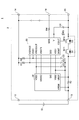
- FIG. 3 is a diagram illustrating an example of a circuit diagram of the battery pack of the present embodiment.
- the battery pack circuit diagram of the related art of FIG. 1 is different from the VBAT connected to the resistor R1 of the secondary battery monitoring IC 130 in that VBAT1 is provided in the protection IC 20 shown in FIG. The difference is that a VBAT 2 connected to the VBAT 1 is provided.
- the description is abbreviate
- the secondary battery 110 in FIG. 1 corresponds to the secondary battery 10 in FIG. 3, and the terminals 112 to 116 in FIG. 1 correspond to the terminals 12 to 16 in FIG. 3, respectively.
- the protection monitoring circuit 2 includes a protection IC (Integrated Circuit) 20 as a protection circuit and a secondary battery monitoring IC 30 as a secondary battery monitoring circuit.
- a protection IC Integrated Circuit
- the protection IC 20 incorporates an overcharge detection circuit, an overdischarge detection circuit, an overcurrent detection circuit, and the like, and detects overcharge, overcurrent, overdischarge, etc. of the secondary battery 10 such as a lithium ion battery, and the like.
- the control transistor provided between the charging device for supplying power to the equal or secondary battery is turned on / off. Thereby, the protection IC 20 protects the secondary battery 10 from overcharge, overcurrent, overdischarge, and the like.
- the protection IC 20 is configured to have VBAT1 which is a terminal connected to VBAT2 of the secondary battery monitoring IC30.
- the protection IC 20 has a voltage dividing circuit 23 connected to VSENSE described later, and divides the battery voltage of the secondary battery 10 input to VSENSE. In addition, the protection IC 20 outputs the divided battery voltage of the secondary battery 10 that is a voltage corresponding to the secondary battery from VBAT 1 to VBAT 2 of the secondary battery monitoring IC 30. Thereby, the protection IC 20 generates a secondary battery corresponding voltage within the withstand voltage range of the secondary battery monitoring IC 30 corresponding to the output voltage of the secondary battery 10.
- the secondary battery monitoring IC 30 is miniaturized and has a withstand voltage lower than the battery voltage of the secondary battery 10. Further, the secondary battery monitoring IC 30 includes a circuit that detects a state of the secondary battery 10 such as a remaining battery level.
- the secondary battery monitoring IC 30 When the secondary battery monitoring IC 30 receives a reference request for status information such as the remaining battery level of the secondary battery 10 from, for example, a portable device, the secondary battery monitoring IC 30 provides the status information corresponding to the reference request to the portable device or the like.
- the secondary battery monitoring IC 30 is configured to have a VBAT 2 that is a voltage detection terminal connected to the VBAT 1 of the protection IC 20.
- the secondary battery monitoring IC 30 obtains a voltage corresponding to the secondary battery within the withstand voltage range of the secondary battery monitoring IC 30 corresponding to the output voltage of the secondary battery 10 generated by the protection IC 20 from the VBAT 2. Detect voltage. A method for detecting the voltage of the secondary battery 10 in the secondary battery monitoring IC 30 will be described later.
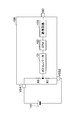
- FIG. 4 is a block diagram for detecting the output voltage of the secondary battery in the present embodiment.
- the protection IC 20 includes a control circuit 21, a switching element 22, a voltage dividing circuit 23, and protection diodes 24 to 25.
- the protection IC 20 includes VSENSE connected to the positive electrode of the secondary battery 10, VSS1 connected to the negative electrode of the secondary battery 10, and VBAT1 connected to VBAT2 of the secondary battery monitoring IC 30.
- the secondary battery monitoring IC 30 includes an AD converter 31, a CPU 32, a nonvolatile memory 33, a communication circuit 34, VBAT 2 connected to VBAT 1 of the protection IC 20, VSS 2 connected to the negative electrode of the secondary battery 10, Communication terminal SIO.
- the protection IC 20 divides the output voltage of the secondary battery 10 input from VSENSE by the voltage dividing circuit 23.
- the voltage dividing circuit 23 includes dividing resistors R8 to R9, and the dividing resistors R8 to R9 are connected in series between VSENSE and VSS1.
- the protection IC 20 divides the output voltage of the secondary battery 10 input from VSENSE by the dividing resistors R8 to R9, thereby responding to the output voltage of the secondary battery 10 from the connection point of the dividing resistor R8 and the dividing resistor R9.
- the voltage corresponding to the secondary battery within the withstand voltage range of the secondary battery monitoring IC 30 is output to the secondary battery monitoring IC 30.
- the secondary battery corresponding voltage corresponding to the output voltage of the secondary battery 10 divided at the connection point between the dividing resistor R8 and the dividing resistor R9 is output from VBAT1 of the protection IC 20 to VBAT2 of the secondary battery monitoring IC 30. .
- the protection IC 20 includes a switching element 22 between VSENSE and the voltage dividing circuit 23.
- the control circuit 21 controls the gate voltage of the control transistor constituting the switching element 32 and turns on the switch of the switching element 32 when measuring the voltage of the secondary battery 10.
- the control circuit 21 can reduce the current consumption by turning off the switch.
- the secondary battery monitoring IC 30 converts the secondary battery corresponding voltage into a digital value by the AD converter 31 and outputs the digital value to the CPU 32.
- the CPU 32 detects the battery voltage of the secondary battery 10 based on the input digital value of the voltage corresponding to the secondary battery. Information on the battery voltage of the secondary battery 10 detected by the CPU 32 is output from the communication terminal SIO to the portable device or the like via the communication circuit 34.
- the secondary battery monitoring IC 30 obtains the voltage corresponding to the secondary battery within the withstand voltage range of the secondary battery monitoring IC 30 corresponding to the output voltage of the secondary battery 10 from the protection IC 20, and the voltage of the secondary battery 10. Can be detected.
- FIG. 5 is a diagram for explaining the output of the AD converter of the secondary battery monitoring IC.
- the protection IC 20 can set the resistance ratio of the dividing resistor R8 and the dividing resistor R9 constituting the voltage dividing circuit 23 to 3: 1, for example.
- the output voltage of the secondary battery 10 is divided into 1 ⁇ 4 by the voltage dividing circuit 23, and the output voltage (secondary battery corresponding voltage) of the secondary battery 10 divided into 1 ⁇ 4 is the secondary battery monitoring IC 30.
- the AD converter 31 To the AD converter 31.
- the AD converter 31 compares the output voltage (secondary battery voltage) of the secondary battery 10 divided into 1 ⁇ 4 with an internal reference voltage, and outputs the difference as a digital value.
- the value of the reference voltage can be set to 800 mV, for example, and the input range of the AD converter 31 can be set to 800 ⁇ 512 mV (288 to 1312 mV), for example.
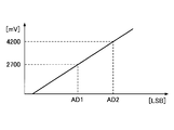
- FIG. 6 is a diagram for explaining a correction method in detection of the secondary battery output voltage of the secondary battery monitoring IC.
- the secondary battery monitoring IC 30 detects the output voltage of the secondary battery 10 using the secondary battery corresponding voltage corresponding to the output voltage of the secondary battery obtained from the protection IC 20.
- the protection IC 20 includes a voltage dividing circuit 23 having a plurality of resistors.
- the resistance value may fluctuate due to variation in the resistance value actually used, temperature change, etc.
- the division value may vary or fluctuate.
- the secondary battery monitoring IC 30 calculates in advance the gain and offset coefficient of the output voltage of the secondary battery that has a linear relationship with the voltage corresponding to the secondary battery in order to measure the accurate output voltage of the secondary battery 10.
- the output voltage of the secondary battery is detected from the voltage corresponding to the secondary battery using the gain and the offset coefficient.
- the input voltage 1 (for example, 2700 mV) and the input voltage 2 (for example, 4200 mV) are applied to VSENSE of the protection IC 20 in advance as an input voltage for calibration.
- the CPU 32 of the secondary battery monitoring IC 30 uses the AD conversion results converted by the AD converter 31 as AD1 and AD2, respectively, using the input voltages 1 and 2 and the AD conversion results AD1 and AD2 to gain G and A correction coefficient for the offset F is obtained.
- the gain G (straight line) is obtained.
- the correction coefficient of the offset F (intersection of the y axis and the straight line) can be obtained as follows.
- the CPU 32 obtains correction coefficients for the gain G and the offset F in advance by the method described above, and stores them in the nonvolatile memory 33, for example.
- the CPU 32 applies a gain G and a digital value (for example, AD conversion result N) converted by the AD converter 31.
- the calculation process is executed as follows using the correction coefficient of the offset F, and the output voltage (for example, the input voltage N) of the secondary battery 10 is calculated.
- Input voltage N AD conversion result N ⁇ gain G + offset F
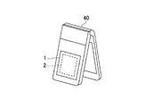
- FIG. 7 is a diagram illustrating an example of a battery pack including the protection monitoring circuit of the present embodiment and a portable device equipped with the battery pack.
- the protection monitoring circuit 2 of this embodiment is provided in the battery pack 1. Moreover, the battery pack 1 provided with the protection monitoring circuit 2 is mounted and used, for example in the portable apparatus 40 grade
- the present embodiment it is possible to detect the output voltage of the secondary battery by the secondary battery monitoring circuit with respect to the decrease in the breakdown voltage accompanying the miniaturization of the circuit, and to improve the electrostatic withstand capability.
- substrate which comprises the protection IC20 mentioned above and the secondary battery monitoring IC30 may generate
- the larger the chip size the more susceptible to the warping of the substrate, and the stress applied to the chip tends to increase toward the end of the chip.
- the chip size of the secondary battery monitoring IC 30 is often larger. Therefore, when the substrate is warped as described above, the secondary battery monitoring IC 30 is more susceptible to the warp of the substrate.
- the voltage dividing circuit is to be mounted on the secondary battery monitoring IC 30, the CPU, memory, and logic blocks are larger than the analog blocks, so it is difficult to place the voltage dividing circuit that is an analog block in the center. Therefore, a situation arises in which the voltage divider circuit must be placed toward the end of the chip that is susceptible to stress.
- the protection IC 20 does not have a large-scale block, it is relatively easy to arrange a voltage dividing circuit in the center of the chip.
- the secondary battery monitoring IC 30 described above can be obtained from the protection IC 20 without directly obtaining power from the secondary battery 10, thereby further reducing the influence of electrostatic discharge from the outside.
Landscapes
- Engineering & Computer Science (AREA)
- Manufacturing & Machinery (AREA)
- Chemical & Material Sciences (AREA)
- Chemical Kinetics & Catalysis (AREA)
- Electrochemistry (AREA)
- General Chemical & Material Sciences (AREA)
- Power Engineering (AREA)
- Secondary Cells (AREA)
- Charge And Discharge Circuits For Batteries Or The Like (AREA)
- Protection Of Static Devices (AREA)
Abstract
Description
図1は、関連技術の電池パックの回路図の一例を示す図である。図1に示すように、電池パック100は、保護監視回路101と、リチウムイオン電池等の充電可能な二次電池110と、二次電池接続正極端子112と、二次電池負極端子113と、外部端子としての正極端子114と、負極端子115とを含む。
次に、図2を用いて、関連技術における二次電池の出力電圧を検出するためのブロック図について説明する。図2は、関連技術における二次電池の出力電圧を検出するためのブロック図である。
図3は、本実施形態の電池パックの回路図の一例を示す図である。上記図1の関連技術の電池パックの回路図とは、二次電池監視IC130の抵抗R1に接続されていたVBATの代わりに、図3に示す保護IC20にVBAT1を設け、二次電池監視IC30にVBAT1と接続されたVBAT2を設けている点で異なる。
次に、図3における保護IC20について説明する。保護IC20は、過充電検出回路、過放電検出回路、及び過電流検出回路等を内蔵して、リチウムイオン電池等の二次電池10の過充電、過電流、過放電等を検出し、携帯機器等又は二次電池に対して電源を供給する充電装置との間に設けられた制御トランジスタをオン/オフ制御する。これにより、保護IC20は、二次電池10を過充電、過電流、過放電等から保護する。
次に、図3における二次電池監視IC30について説明する。二次電池監視IC30は、微細化され、二次電池10の電池電圧未満の耐圧となっている。また、二次電池監視IC30は、二次電池10の電池残量等の状態を検出する回路を含む。
次に、図4を参照して、本実施形態における二次電池の出力電圧を検出するためのブロック図について説明する。図4は、本実施形態における二次電池の出力電圧を検出するためのブロック図である。
次に、二次電池監視IC30のADコンバータ31の出力について説明をする。図5は、二次電池監視ICのADコンバータの出力について説明するための図である。
次に、二次電池監視IC30の二次電池出力電圧の検出における補正方法について説明する。図6は、二次電池監視ICの二次電池出力電圧の検出における補正方法を説明するための図である。
オフセットF=-ゲインG×AD1+2700
CPU32は、上述した方法で予めゲインG、オフセットFの補正係数を求め、例えば不揮発性メモリ33等に格納しておく。CPU32は、保護IC20から二次電圧10の出力電圧に対応する二次電池対応電圧が入力されたとき、ADコンバータ31によって変換されたデジタル値(例えばAD変換結果N)に対して、ゲインG及びオフセットFの補正係数を用いて以下のように演算処理を実行し、二次電池10の出力電圧(例えば入力電圧N)を算出する。
これにより、二次電池監視IC30は、例えば保護IC20の抵抗値にばらつきが生じた場合でも、このばらつきを補正して、保護IC20から得た二次電池対応電圧から二次電池10の正確な出力電圧を検出することが可能となる。
次に、図7を参照して、本実施形態の保護監視回路2を備えた電池パック1、及び該電池パック1を搭載した携帯機器40について説明する。図7は、本実施形態の保護監視回路を備えた電池パック、及び該電池パックを搭載した携帯機器の一例を示す図である。
なお本出願は、日本特許庁に2010年2月22日に出願された基礎出願第2010-036671号に基づくものであり、その全内容はここに参照により含まれる。
2,101 保護監視回路
12,112 二次電池接続正極端子
13,113 二次電池負極端子
14,114 正極端子
15,115 負極端子
16,116 外部端子
20,120 保護IC
21 制御回路
22 スイッチング素子
23 電圧分割回路
24,25 保護ダイオード
30,130 二次電池監視IC
31,131 ADコンバータ
32,132 CPU
33 不揮発性メモリ
34,133 通信回路
40 携帯機器
Claims (5)
- 充電可能な二次電池の過充電、過放電、及び過電流のうち少なくとも一つを検出して、制御トランジスタをオン/オフ制御することにより前記二次電池を保護する保護回路と、
前記二次電池の電池電圧未満の耐圧を有し、前記二次電池の状態を検出する微細化された二次電池監視回路と
を含み、
前記保護回路は、前記二次電池の出力電圧に応じた前記二次電池監視回路の耐圧範囲内の電圧を生成し、
前記二次電池監視回路は、前記保護回路から供給される前記生成された電圧に応じた検出値を生成し、前記検出値は前記二次電池の出力電圧を示すことを特徴とする保護監視回路。 - 前記保護回路は、前記二次電池の出力電圧を受け取る電圧端子と、該電圧端子に接続される電圧分割回路とを有することを特徴とする請求項1に記載の保護監視回路。
- 前記保護回路は、前記電圧端子と前記電圧分割回路との間にスイッチング素子を有することを特徴とする請求項2に記載の保護監視回路。
- 前記二次電池監視回路は、前記生成された電圧と直線関係にある前記二次電池の出力電圧のゲイン及びオフセット係数を予め算出し、前記算出したゲイン及びオフセット係数を用いて、前記生成された電圧から前記検出値を生成することを特徴とする請求項1記載の保護監視回路。
- 二次電池と、
保護監視回路と
を含み、前記保護監視回路は、
充電可能な二次電池の過充電、過放電、及び過電流のうち少なくとも一つを検出して、制御トランジスタをオン/オフ制御することにより前記二次電池を保護する保護回路と、
前記二次電池の電池電圧未満の耐圧を有し、前記二次電池の状態を検出する微細化された二次電池監視回路と
を含み、
前記保護回路は、前記二次電池の出力電圧に応じた前記二次電池監視回路の耐圧範囲内の電圧を生成し、
前記二次電池監視回路は、前記保護回路から供給される前記生成された電圧に応じた検出値を生成し、前記検出値は前記二次電池の出力電圧を示すことを特徴とする電池パック。
Priority Applications (3)
| Application Number | Priority Date | Filing Date | Title |
|---|---|---|---|
| US13/579,317 US8773830B2 (en) | 2010-02-22 | 2011-02-15 | Protective monitoring circuit and battery pack |
| CN201180010279.6A CN102782977B (zh) | 2010-02-22 | 2011-02-15 | 保护监视电路和电池组 |
| US14/247,343 US9293930B2 (en) | 2010-02-22 | 2014-04-08 | Protective monitoring circuit and battery pack |
Applications Claiming Priority (3)
| Application Number | Priority Date | Filing Date | Title |
|---|---|---|---|
| JP2010-036671 | 2010-02-22 | ||
| JP2010036671A JP5504964B2 (ja) | 2010-02-22 | 2010-02-22 | 保護監視回路、及び電池パック |
| JP2014051556A JP5598623B2 (ja) | 2010-02-22 | 2014-03-14 | 保護監視回路、及び電池パック |
Related Child Applications (2)
| Application Number | Title | Priority Date | Filing Date |
|---|---|---|---|
| US13/579,317 A-371-Of-International US8773830B2 (en) | 2010-02-22 | 2011-02-15 | Protective monitoring circuit and battery pack |
| US14/247,343 Division US9293930B2 (en) | 2010-02-22 | 2014-04-08 | Protective monitoring circuit and battery pack |
Publications (1)
| Publication Number | Publication Date |
|---|---|
| WO2011102338A1 true WO2011102338A1 (ja) | 2011-08-25 |
Family
ID=59519902
Family Applications (1)
| Application Number | Title | Priority Date | Filing Date |
|---|---|---|---|
| PCT/JP2011/053128 Ceased WO2011102338A1 (ja) | 2010-02-22 | 2011-02-15 | 保護監視回路、及び電池パック |
Country Status (4)
| Country | Link |
|---|---|
| US (2) | US8773830B2 (ja) |
| JP (2) | JP5504964B2 (ja) |
| CN (1) | CN102782977B (ja) |
| WO (1) | WO2011102338A1 (ja) |
Cited By (1)
| Publication number | Priority date | Publication date | Assignee | Title |
|---|---|---|---|---|
| CN103701163A (zh) * | 2013-12-06 | 2014-04-02 | 深圳市大疆创新科技有限公司 | 电池、具有该电池的飞行器及电池控制方法 |
Families Citing this family (9)
| Publication number | Priority date | Publication date | Assignee | Title |
|---|---|---|---|---|
| EP2815482B1 (en) * | 2012-02-14 | 2018-05-16 | Nokia Technologies Oy | Method and circuitry for battery protection |
| WO2014045745A1 (ja) * | 2012-09-18 | 2014-03-27 | Necエナジーデバイス株式会社 | 蓄電システムおよび電池保護方法 |
| US9302595B2 (en) * | 2013-01-16 | 2016-04-05 | Ford Global Technologies, Llc | Autonomous charge balancing circuit and method for battery pack |
| DE102013217458A1 (de) * | 2013-09-02 | 2015-03-05 | Robert Bosch Gmbh | Schützbaugruppe für eine elektrochemische Zellen umfassende Hochvolt-Speichereinheit |
| CN104810878B (zh) | 2014-01-28 | 2017-05-10 | 广东欧珀移动通信有限公司 | 过压过流保护电路和移动终端 |
| JP2016218978A (ja) * | 2015-05-26 | 2016-12-22 | 富士通株式会社 | 電子機器及び電子機器制御方法 |
| JP6372437B2 (ja) * | 2015-07-30 | 2018-08-15 | ミツミ電機株式会社 | マルチチップ、電池保護装置及び電池パック |
| JP6460218B1 (ja) * | 2017-12-08 | 2019-01-30 | ミツミ電機株式会社 | 二次電池保護集積回路、二次電池保護装置及び電池パック |
| KR102575045B1 (ko) * | 2018-01-09 | 2023-09-05 | 현대모비스 주식회사 | 배터리 충전기 최적효율 제어방법 및 이를 채용한 충전기 |
Citations (3)
| Publication number | Priority date | Publication date | Assignee | Title |
|---|---|---|---|---|
| JP2000014027A (ja) * | 1998-06-23 | 2000-01-14 | Hitachi Ltd | 蓄電器制御装置 |
| JP2000295776A (ja) * | 1999-04-08 | 2000-10-20 | Seiko Instruments Inc | バッテリー状態監視回路及びバッテリー装置 |
| JP2009153238A (ja) * | 2007-12-18 | 2009-07-09 | Mitsumi Electric Co Ltd | 携帯機器と、携帯機器に用いる電池パック |
Family Cites Families (9)
| Publication number | Priority date | Publication date | Assignee | Title |
|---|---|---|---|---|
| JPH11308776A (ja) * | 1998-04-21 | 1999-11-05 | Seiko Instruments Inc | バッテリー状態監視回路及びバッテリー装置 |
| US6137265A (en) * | 1999-01-11 | 2000-10-24 | Dell Usa, L.P. | Adaptive fast charging of lithium-ion batteries |
| EP1320168A1 (en) * | 2001-12-12 | 2003-06-18 | Dialog Semiconductor GmbH | Power switch for battery protection |
| JP3859608B2 (ja) * | 2003-03-31 | 2006-12-20 | 富士通株式会社 | 電池パック、電子機器、電池残量予測システム及び半導体装置 |
| JP2005160169A (ja) | 2003-11-21 | 2005-06-16 | Texas Instr Japan Ltd | バッテリ保護回路 |
| WO2007007655A1 (ja) * | 2005-07-07 | 2007-01-18 | Kabushiki Kaisha Toshiba | 電池システム |
| US7615969B2 (en) * | 2006-07-27 | 2009-11-10 | Dell Products L.P. | Systems and methods for temperature-dependent battery charging |
| JP4503636B2 (ja) * | 2007-08-28 | 2010-07-14 | レノボ・シンガポール・プライベート・リミテッド | 電池パックおよび充電方法 |
| US8264200B2 (en) * | 2009-05-15 | 2012-09-11 | Texas Instruments Incorporated | Multi-cell power system controller |
-
2010
- 2010-02-22 JP JP2010036671A patent/JP5504964B2/ja not_active Expired - Fee Related
-
2011
- 2011-02-15 CN CN201180010279.6A patent/CN102782977B/zh not_active Expired - Fee Related
- 2011-02-15 WO PCT/JP2011/053128 patent/WO2011102338A1/ja not_active Ceased
- 2011-02-15 US US13/579,317 patent/US8773830B2/en active Active
-
2014
- 2014-03-14 JP JP2014051556A patent/JP5598623B2/ja not_active Expired - Fee Related
- 2014-04-08 US US14/247,343 patent/US9293930B2/en active Active
Patent Citations (3)
| Publication number | Priority date | Publication date | Assignee | Title |
|---|---|---|---|---|
| JP2000014027A (ja) * | 1998-06-23 | 2000-01-14 | Hitachi Ltd | 蓄電器制御装置 |
| JP2000295776A (ja) * | 1999-04-08 | 2000-10-20 | Seiko Instruments Inc | バッテリー状態監視回路及びバッテリー装置 |
| JP2009153238A (ja) * | 2007-12-18 | 2009-07-09 | Mitsumi Electric Co Ltd | 携帯機器と、携帯機器に用いる電池パック |
Cited By (6)
| Publication number | Priority date | Publication date | Assignee | Title |
|---|---|---|---|---|
| CN103701163A (zh) * | 2013-12-06 | 2014-04-02 | 深圳市大疆创新科技有限公司 | 电池、具有该电池的飞行器及电池控制方法 |
| CN103701163B (zh) * | 2013-12-06 | 2018-05-01 | 深圳市大疆创新科技有限公司 | 电池、具有该电池的飞行器及电池控制方法 |
| US10525832B2 (en) | 2013-12-06 | 2020-01-07 | SZ DJI Technology Co., Ltd. | Battery and unmanned aerial vehicle with the battery |
| US10625613B2 (en) | 2013-12-06 | 2020-04-21 | SZ DJI Technology Co., Ltd. | Battery and unmanned aerial vehicle with the battery |
| US10906427B2 (en) | 2013-12-06 | 2021-02-02 | SZ DJI Technology Co., Ltd. | Battery and unmanned aerial vehicle with the battery |
| US11607972B2 (en) | 2013-12-06 | 2023-03-21 | SZ DJI Technology Co., Ltd. | Battery and unmanned aerial vehicle with battery indicator and venting opening |
Also Published As
| Publication number | Publication date |
|---|---|
| CN102782977B (zh) | 2015-06-24 |
| JP5598623B2 (ja) | 2014-10-01 |
| US8773830B2 (en) | 2014-07-08 |
| US9293930B2 (en) | 2016-03-22 |
| US20140217990A1 (en) | 2014-08-07 |
| JP2011172458A (ja) | 2011-09-01 |
| JP2014143914A (ja) | 2014-08-07 |
| CN102782977A (zh) | 2012-11-14 |
| JP5504964B2 (ja) | 2014-05-28 |
| US20120300351A1 (en) | 2012-11-29 |
Similar Documents
| Publication | Publication Date | Title |
|---|---|---|
| JP5598623B2 (ja) | 保護監視回路、及び電池パック | |
| US8305041B2 (en) | Battery pack | |
| JP6187610B2 (ja) | 二次電池監視装置および電池パック | |
| US8471526B2 (en) | Protection device for secondary batteries, and battery pack and electronic equipment employing same | |
| US9553469B2 (en) | Method of overcurrent detection voltage correction and battery protection integrated circuit | |
| US20100201327A1 (en) | Battery pack | |
| JP2009153238A (ja) | 携帯機器と、携帯機器に用いる電池パック | |
| JP7039124B2 (ja) | 充放電制御装置、及びバッテリ装置 | |
| US8524385B2 (en) | Battery pack | |
| WO2010055785A1 (ja) | 保護回路及び電池パック | |
| JP2009077610A (ja) | 充放電保護回路および電池パック | |
| CN110896212B (zh) | 二次电池保护电路 | |
| US20070164710A1 (en) | Abnormality detection apparatus for secondary battery device | |
| JP2009044824A (ja) | 電池パック | |
| KR20170087336A (ko) | 배터리 보호 회로 및 그것을 포함하는 웨어러블 디바이스 | |
| KR102220900B1 (ko) | 배터리 보호회로 및 이를 포함한 배터리 팩 | |
| US7501796B2 (en) | Semiconductor device having positive side of power supply voltage set | |
| US8867246B2 (en) | Communication device and battery pack in which the communication device is provided |
Legal Events
| Date | Code | Title | Description |
|---|---|---|---|
| WWE | Wipo information: entry into national phase |
Ref document number: 201180010279.6 Country of ref document: CN |
|
| 121 | Ep: the epo has been informed by wipo that ep was designated in this application |
Ref document number: 11744624 Country of ref document: EP Kind code of ref document: A1 |
|
| WWE | Wipo information: entry into national phase |
Ref document number: 13579317 Country of ref document: US |
|
| NENP | Non-entry into the national phase |
Ref country code: DE |
|
| 122 | Ep: pct application non-entry in european phase |
Ref document number: 11744624 Country of ref document: EP Kind code of ref document: A1 |