WO2011092894A1 - Dispositif d'éclairage et écran - Google Patents
Dispositif d'éclairage et écran Download PDFInfo
- Publication number
- WO2011092894A1 WO2011092894A1 PCT/JP2010/066777 JP2010066777W WO2011092894A1 WO 2011092894 A1 WO2011092894 A1 WO 2011092894A1 JP 2010066777 W JP2010066777 W JP 2010066777W WO 2011092894 A1 WO2011092894 A1 WO 2011092894A1
- Authority
- WO
- WIPO (PCT)
- Prior art keywords
- light emitting
- light
- lighting device
- emitting device
- substrate
- Prior art date
Links
Images


Classifications
-
- G—PHYSICS
- G09—EDUCATION; CRYPTOGRAPHY; DISPLAY; ADVERTISING; SEALS
- G09G—ARRANGEMENTS OR CIRCUITS FOR CONTROL OF INDICATING DEVICES USING STATIC MEANS TO PRESENT VARIABLE INFORMATION
- G09G3/00—Control arrangements or circuits, of interest only in connection with visual indicators other than cathode-ray tubes
- G09G3/20—Control arrangements or circuits, of interest only in connection with visual indicators other than cathode-ray tubes for presentation of an assembly of a number of characters, e.g. a page, by composing the assembly by combination of individual elements arranged in a matrix no fixed position being assigned to or needed to be assigned to the individual characters or partial characters
- G09G3/34—Control arrangements or circuits, of interest only in connection with visual indicators other than cathode-ray tubes for presentation of an assembly of a number of characters, e.g. a page, by composing the assembly by combination of individual elements arranged in a matrix no fixed position being assigned to or needed to be assigned to the individual characters or partial characters by control of light from an independent source
- G09G3/3406—Control of illumination source
- G09G3/342—Control of illumination source using several illumination sources separately controlled corresponding to different display panel areas, e.g. along one dimension such as lines
- G09G3/3426—Control of illumination source using several illumination sources separately controlled corresponding to different display panel areas, e.g. along one dimension such as lines the different display panel areas being distributed in two dimensions, e.g. matrix
-
- G—PHYSICS
- G02—OPTICS
- G02F—OPTICAL DEVICES OR ARRANGEMENTS FOR THE CONTROL OF LIGHT BY MODIFICATION OF THE OPTICAL PROPERTIES OF THE MEDIA OF THE ELEMENTS INVOLVED THEREIN; NON-LINEAR OPTICS; FREQUENCY-CHANGING OF LIGHT; OPTICAL LOGIC ELEMENTS; OPTICAL ANALOGUE/DIGITAL CONVERTERS
- G02F1/00—Devices or arrangements for the control of the intensity, colour, phase, polarisation or direction of light arriving from an independent light source, e.g. switching, gating or modulating; Non-linear optics
- G02F1/01—Devices or arrangements for the control of the intensity, colour, phase, polarisation or direction of light arriving from an independent light source, e.g. switching, gating or modulating; Non-linear optics for the control of the intensity, phase, polarisation or colour
- G02F1/13—Devices or arrangements for the control of the intensity, colour, phase, polarisation or direction of light arriving from an independent light source, e.g. switching, gating or modulating; Non-linear optics for the control of the intensity, phase, polarisation or colour based on liquid crystals, e.g. single liquid crystal display cells
- G02F1/133—Constructional arrangements; Operation of liquid crystal cells; Circuit arrangements
- G02F1/1333—Constructional arrangements; Manufacturing methods
- G02F1/1335—Structural association of cells with optical devices, e.g. polarisers or reflectors
- G02F1/1336—Illuminating devices
- G02F1/133602—Direct backlight
- G02F1/133603—Direct backlight with LEDs
-
- G—PHYSICS
- G02—OPTICS
- G02F—OPTICAL DEVICES OR ARRANGEMENTS FOR THE CONTROL OF LIGHT BY MODIFICATION OF THE OPTICAL PROPERTIES OF THE MEDIA OF THE ELEMENTS INVOLVED THEREIN; NON-LINEAR OPTICS; FREQUENCY-CHANGING OF LIGHT; OPTICAL LOGIC ELEMENTS; OPTICAL ANALOGUE/DIGITAL CONVERTERS
- G02F1/00—Devices or arrangements for the control of the intensity, colour, phase, polarisation or direction of light arriving from an independent light source, e.g. switching, gating or modulating; Non-linear optics
- G02F1/01—Devices or arrangements for the control of the intensity, colour, phase, polarisation or direction of light arriving from an independent light source, e.g. switching, gating or modulating; Non-linear optics for the control of the intensity, phase, polarisation or colour
- G02F1/13—Devices or arrangements for the control of the intensity, colour, phase, polarisation or direction of light arriving from an independent light source, e.g. switching, gating or modulating; Non-linear optics for the control of the intensity, phase, polarisation or colour based on liquid crystals, e.g. single liquid crystal display cells
- G02F1/133—Constructional arrangements; Operation of liquid crystal cells; Circuit arrangements
- G02F1/1333—Constructional arrangements; Manufacturing methods
- G02F1/1335—Structural association of cells with optical devices, e.g. polarisers or reflectors
- G02F1/1336—Illuminating devices
- G02F1/133602—Direct backlight
- G02F1/133605—Direct backlight including specially adapted reflectors
-
- H—ELECTRICITY
- H05—ELECTRIC TECHNIQUES NOT OTHERWISE PROVIDED FOR
- H05B—ELECTRIC HEATING; ELECTRIC LIGHT SOURCES NOT OTHERWISE PROVIDED FOR; CIRCUIT ARRANGEMENTS FOR ELECTRIC LIGHT SOURCES, IN GENERAL
- H05B45/00—Circuit arrangements for operating light-emitting diodes [LED]
- H05B45/10—Controlling the intensity of the light
- H05B45/12—Controlling the intensity of the light using optical feedback
-
- H—ELECTRICITY
- H05—ELECTRIC TECHNIQUES NOT OTHERWISE PROVIDED FOR
- H05B—ELECTRIC HEATING; ELECTRIC LIGHT SOURCES NOT OTHERWISE PROVIDED FOR; CIRCUIT ARRANGEMENTS FOR ELECTRIC LIGHT SOURCES, IN GENERAL
- H05B45/00—Circuit arrangements for operating light-emitting diodes [LED]
- H05B45/10—Controlling the intensity of the light
- H05B45/18—Controlling the intensity of the light using temperature feedback
-
- G—PHYSICS
- G02—OPTICS
- G02F—OPTICAL DEVICES OR ARRANGEMENTS FOR THE CONTROL OF LIGHT BY MODIFICATION OF THE OPTICAL PROPERTIES OF THE MEDIA OF THE ELEMENTS INVOLVED THEREIN; NON-LINEAR OPTICS; FREQUENCY-CHANGING OF LIGHT; OPTICAL LOGIC ELEMENTS; OPTICAL ANALOGUE/DIGITAL CONVERTERS
- G02F2201/00—Constructional arrangements not provided for in groups G02F1/00 - G02F7/00
- G02F2201/58—Arrangements comprising a monitoring photodetector
-
- G—PHYSICS
- G09—EDUCATION; CRYPTOGRAPHY; DISPLAY; ADVERTISING; SEALS
- G09G—ARRANGEMENTS OR CIRCUITS FOR CONTROL OF INDICATING DEVICES USING STATIC MEANS TO PRESENT VARIABLE INFORMATION
- G09G2360/00—Aspects of the architecture of display systems
- G09G2360/14—Detecting light within display terminals, e.g. using a single or a plurality of photosensors
- G09G2360/145—Detecting light within display terminals, e.g. using a single or a plurality of photosensors the light originating from the display screen
Definitions
- the present invention relates to a lighting device and a display device, and more particularly to a lighting device and a display device including a plurality of substrates on which light emitting devices are mounted.
- a backlight device including a substrate on which a light emitting device such as an LED (Light Emitting Diode) is mounted is known.
- a method of arranging a large number of substrates on which light emitting devices are mounted is often used.
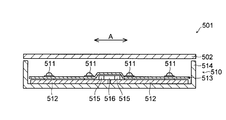
- FIG. 7 is a cross-sectional view showing a structure of a display device including a backlight device (illumination device) according to a conventional example including a plurality of substrates on which LEDs (light emitting devices) are mounted.
- FIG. 8 is a plan view of the backlight device according to the conventional example shown in FIG. 7 excluding the reflection sheet (reflection member).
- the backlight device 510 includes a plurality of LEDs (light emitting devices) 511, a plurality of substrates 512 on which the plurality of LEDs 511 are mounted, and a reflective sheet disposed on the plurality of substrates 512. 513 (refer FIG. 7) and the chassis 514 which accommodates these.
- the LED 511 is configured to emit white light and functions as a light source of the backlight device 510.
- the LED 511 is electrically connected to the substrate 512.
- An FPC (Flexible Printed Circuit) connector 515 is provided at an end of the substrate 512 in the longitudinal direction (A direction).
- An FPC 516 is attached to the FPC connector 515, and adjacent substrates 512 are electrically connected to each other. Thereby, various information can be transmitted (communication) between adjacent substrates 512.
- an opening is formed in the portion of the reflection sheet 513 where the LED 511 is located, and the light emitting portion (hemispherical portion) of the LED 511 is located above (display panel) through this opening. 502 side).
- the reflection sheet 513 is disposed so as to cover the FPC connector 515 and the FPC 516.
- the reflection sheet 513 has a function of reflecting the light emitted from the LED 511 and reflected by the display panel 502 or the like to the display panel 502 side.
- Patent Document 1 a backlight device in which adjacent substrates are connected by a wiring member such as an FPC is disclosed in Patent Document 1, for example.
- the reflection sheet 513 is disposed so as to cover the FPC connector 515 and the FPC 516.
- the sheet 513 floats. That is, the reflection sheet 513 is bent. For this reason, there is a problem that luminance unevenness occurs in the display panel 502.
- the FPC connector 515 and the FPC 516 In order to prevent the reflection sheet 513 from floating (deflection), even if an opening is formed in the portion of the reflection sheet 513 where the FPC connector 515 and the FPC 516 are located, the FPC connector 515 and the FPC 516 (on the reflection) The luminance of the portion of the display panel 502 on the opening of the sheet 513 decreases, and uneven luminance occurs in the display panel 502.
- the present invention has been made to solve the above-described problems, and an object of the present invention is to provide an illuminating device and a display device capable of suppressing occurrence of luminance unevenness in an illuminated member. It is to be.
- an illumination device includes at least a plurality of light emitting devices that emit visible light, a plurality of substrates on which the light emitting devices are mounted, a substrate mounted on the substrate, and a light A light receiving element that receives light and a reflective member disposed on the substrate, and a first opening or a notch is formed in a portion of the reflective member where the light emitting device and the light receiving element are located. It functions as a light source for illumination and transmits an optical signal to a light receiving element mounted on an adjacent substrate, and the light receiving element receives an optical signal from a light emitting device mounted on the adjacent substrate.
- the light emitting device and the light receiving element are provided on the substrate, and the light emitting device is configured to transmit an optical signal to the light receiving element mounted on the adjacent substrate.
- the light receiving element is configured to receive an optical signal from a light emitting device mounted on an adjacent substrate.
- a first opening or a notch is formed in the portion of the reflecting member where the light emitting device and the light receiving element are located.
- the light receiving element is sufficiently smaller than the FPC or the FPC connector, even if the first opening or the notch is provided in the part of the reflecting member where the light receiving element is located, It is possible to sufficiently suppress the luminance of the portion of the illuminated member (on one opening or notch) from being lowered, and to suppress occurrence of luminance unevenness in the illuminated member.
- the light emitting device functions as a light source for illumination, and transmits an optical signal to a light receiving element mounted on an adjacent substrate. Accordingly, it is not necessary to separately provide a light emitting device for transmitting an optical signal in order to transmit an optical signal to a light receiving element mounted on an adjacent substrate. For this reason, it can suppress that a number of parts increases.
- the optical signal preferably includes a visible light signal. If comprised in this way, the general light-emitting device currently used as the light source for illumination can be used as it is as the light-emitting device for optical signal transmission.
- the light emitting device is driven on and off in a frequency band in which blinking of the light emitting device cannot be visually recognized, so that the visible light signal is converted into an adjacent substrate. It transmits to the light receiving element mounted on. If comprised in this way, a light-emitting device can be blinked in the frequency band which cannot visually recognize blinking of a light-emitting device. Thereby, it can prevent that a to-be-illuminated member will blink and appear by the afterimage phenomenon.
- the lighting device further includes a control unit that controls the light emitting device, a control board on which the control unit is mounted, and a light emitting unit mounted on the control board, An optical signal is transmitted to at least some of the light receiving elements. If comprised in this way, optical communication can be performed between a control board and a board
- control board and the board by performing optical communication between the control board and the board, it is not necessary to connect the control board and the board using an FPC or an FPC connector. For this reason, unlike the case where the control board and the board are connected using an FPC or FPC connector, it is possible to prevent the reflecting member from floating (bending) in the region where the FPC or FPC connector is arranged. . As a result, it is possible to further suppress the occurrence of luminance unevenness in the illuminated member.
- the communication speed between the control board and the board can be increased, and communication between the control board and the board can be performed with other circuits. It can be made not to be influenced by electromagnetic waves generated in the. In addition, since it is not necessary to connect the FPC and the FPC connector between the control board and the board, it is possible to more easily assemble, disassemble and repair the lighting device.
- the lighting device including the control unit, the control board, and the light emitting unit preferably further includes a light receiving unit mounted on the control board, and the light receiving unit receives an optical signal from at least a part of the light emitting devices. If comprised in this way, bidirectional
- the lighting device including the control unit, the control board, and the light emitting unit
- the lighting device further includes a plurality of light emitting devices and a chassis that houses the plurality of boards, the control board is disposed outside the chassis, and the light emitting unit includes A second opening is formed in the portion of the chassis located. If comprised in this way, even if it is a case where a control board is arrange
- the light emitting device includes a light emitting diode. If comprised in this way, a light-emitting device can be reduced in size easily. In addition, since a semiconductor light emitting device such as a light emitting diode has a fast on / off response speed (for example, 10 nsec or less), the light emitting device can be easily driven on and off at high speed.
- the light emitting device may be configured to include a white light emitting diode.
- the light emitting device may include a red light emitting diode element, a green light emitting diode element, and a blue light emitting diode element.
- the light receiving element includes a photodiode. If comprised in this way, a light receiving element can be reduced in size easily.
- the lighting device preferably further includes a power adjusting unit that adjusts the amount of power supplied to the light emitting device.
- a power adjusting unit that adjusts the amount of power supplied to the light emitting device.
- the lighting device may further include a brightness improving member that is disposed on the light emitting device and that improves the brightness of the illuminated member that is illuminated by the light emitting device.
- the lighting device may further include a light diffusion layer that is disposed on the light emitting device and diffuses light emitted from the light emitting device.
- the lighting device preferably functions as a backlight device for illuminating the display panel. If comprised in this way, the illuminating device (backlight apparatus) which can suppress that the brightness
- the present invention it is possible to easily obtain an illuminating device and a display device capable of suppressing occurrence of luminance unevenness in a member to be illuminated.
- FIG. 2 is a plan view for explaining the structure of the backlight device according to the embodiment of the present invention shown in FIG. 1.
- FIG. 2 is a cross-sectional view illustrating the structure of the backlight device according to the embodiment of the present invention illustrated in FIG. 1.
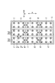
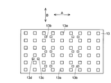
- FIG. 2 is a plan view illustrating a structure of a reflection sheet of the backlight device according to the embodiment of the present invention illustrated in FIG. 1.
- FIG. 2 is a cross-sectional view illustrating the structure of the backlight device according to the embodiment of the present invention illustrated in FIG. 1.
- FIG. 8 is a plan view of the backlight device according to the conventional example shown in FIG. 7 excluding a reflection sheet.
- the backlight device 10 is disposed on the front side (upper side) of the reflection sheet 13, the plurality of LEDs 11, the plurality of substrates 12 on which the plurality of LEDs 11 are mounted, the reflection sheet 13 disposed on the plurality of substrates 12.
- a diffusion plate 14 and a plurality of optical sheets 15, and a front chassis 16 and a back chassis 17 that store them are provided.
- the LED 11 is an example of the “light emitting device”, “light emitting diode”, and “white light emitting diode” in the present invention
- the reflection sheet 13 is an example of the “reflecting member” in the present invention.
- the diffusion plate 14 is an example of the “light diffusion layer” in the present invention
- the optical sheet 15 is an example of the “brightness improving member” in the present invention.
- the back chassis 17 is an example of the “chassis” in the present invention.
- each LED 11 is mounted on the front surface (upper surface) of each substrate 12 along the A direction (longitudinal direction of the substrate 12), and in the B direction (substrate). (E.g., 12 lateral directions), for example, two each.
- the LED 11 is electrically connected to the substrate 12.
- the LED 11 has a hemispherical lens portion. This lens unit has a function of diffusing and emitting light.
- the LED 11 includes, for example, a red light emitting diode element that emits red light, a green light emitting diode element that emits green light, and a blue light emitting diode element that emits blue light.
- white light is radiate
- the LED 11 is configured to be driven on and off in a frequency band in which the blinking of the LED 11 cannot be visually recognized.
- the light emitted from the LED 11 by being turned on / off in this frequency band functions as a visible light signal, and is received by a photodiode 18 described later mounted on the adjacent substrate 12.
- the visible light signal includes various information (luminance information, temperature information, control information, etc.) transmitted (communication) between the substrates 12 and the like.
- Luminance information is information for increasing or decreasing the light emission amount of each LED 11, for example. More specifically, the luminance information increases the light emission amount of the LED 11 by increasing the current applied to the LED 11 in the area where the bright image is displayed in accordance with the image displayed on the liquid crystal display panel 3, or other areas. This is used to reduce the amount of light emitted from the LED 11 by reducing the current applied to the LED 11 (or turning off the LED 11).
- the temperature information is information obtained by a temperature sensor (not shown) provided on the substrate 12, for example. Specifically, the temperature information is information for detecting the temperature on each substrate 12, and is used to reduce the light emission amount of the LED 11 on the substrate 12 having a high temperature and suppress the heat generation caused by the LED 11. .
- the control information is information for controlling the interval of blinking (turning on and off) of the LED 11, for example.
- the frequency band (carrier frequency) at which the LED 11 is driven on and off can be set to, for example, about 28.8 kHz, but is not particularly limited as long as it is impossible to visually recognize the blinking of the LED 11.
- the LED 11 is driven on and off in the above frequency band by a visible light signal from the adjacent substrate 12 and a visible light signal from the control substrate 21 described later.
- red light emitting diode element only one of the red light emitting diode element, the green light emitting diode element, and the blue light emitting diode element may be configured to be turned on / off in the frequency band described above, or the red light emitting diode element and the green light emitting diode may be configured. Two or three of the element and the blue light emitting diode element may be configured to be turned on / off in the above frequency band.
- luminance information, temperature information, control information, and the like may be included in only one of red light, green light, and blue light, or luminance information, temperature information, control information, and the like are red.
- luminance information, temperature information, control information, and the like are red.
- One each of light, green light and blue light may be included.
- the LED 11 functions as a light source for illumination, and is configured to transmit a visible light signal to the photodiode 18 mounted on the adjacent substrate 12.
- the substrates 12 are arranged, for example, three by three along the A direction and the B direction.
- one or two photodiodes 18 are mounted on the front surface (upper surface) of the substrate 12.
- the photodiode 18 is electrically connected to the substrate 12.
- the photodiode 18 has an outer shape smaller than that of the LED 11 when viewed in plan.
- the photodiode 18 is an example of the “light receiving element” in the present invention.
- the photodiode 18 is configured to receive a visible light signal from the LED 11 mounted on the adjacent substrate 12. Thereby, various information (luminance information, temperature information, control information, etc.) can be transmitted (communication) between adjacent substrates 12.
- the backlight device 10 is configured to perform visible light communication between adjacent substrates 12.
- the plurality of optical sheets 15 are configured by, for example, DBEF (trade name) manufactured by Sumitomo 3M Limited, a microlens sheet, various prism sheets, and the like, and the light transmitted through the diffusion plate 14 has a predetermined viewing angle. It has a function of condensing and improving the luminance of the liquid crystal display panel 3.
- the back chassis 17 is made of metal. As shown in FIG. 5, the back chassis 17 is electrically connected to the negative electrode of the power source 19 a mounted on the power board 19 disposed outside the back chassis 17.
- the power supply board 19 is also equipped with a control unit 19b for controlling the power supply 19a.
- the control unit 19b has a function of adjusting the amount of power supplied to the LED 11.
- the power supply board 19 may be electrically connected to a control board 21 to be described later, or the power supply board 19 and the control board 21 may be configured integrally. Moreover, you may incorporate the function of the control part 19b in the control part 22 mentioned later.
- the control unit 19b is an example of the “power adjustment unit” in the present invention.
- the substrate 12 is fixed to the back chassis 17 by using conductive screws 20.
- the screw 20 electrically connects a negative wiring (or ground wiring) (not shown) of the substrate 12 and the back chassis 17.
- the positive electrode of the power source 19a is electrically connected to the positive electrode wiring of the board
- a control board 21 is disposed on the back side (outside) of the back chassis 17.
- a control unit 22 that controls the LED 11, an LED 23, and a photodiode 24 are mounted on the control board 21, a control unit 22 that controls the LED 11, an LED 23, and a photodiode 24 are mounted.
- the LED 23 is an example of the “light emitting unit” in the present invention
- the photodiode 24 is an example of the “light receiving unit” in the present invention.
- openings 17a and 17b are provided in the portion of the back chassis 17 where the LED 23 and the photodiode 24 are located.
- the control unit 22 is configured to input a control signal to the LED 23 and drive the LED 23 on and off in a frequency band in which the blinking of the LED 23 is not visible.
- the LED 23 is configured to be turned on and off by a control signal from the control unit 22, for example, in a frequency band of about 28.8 kHz.
- the light emitted from the LED 23 functions as a visible light signal and is received by the photodiode 18 mounted on the substrate 12a (see FIGS. 2 and 3) disposed in the vicinity of the control substrate 21.
- the visible light signal includes various information (such as luminance information, temperature information, and control information) transmitted (communication) between the control board 21 and the board 12.
- the LED 23 is configured by, for example, a red light emitting diode element that emits red light, a green light emitting diode element that emits green light, and a blue light emitting diode element that emits blue light, as in the LED 11. Also good. Further, unlike the LED 11, the LED 23 may be configured by any one of a red light emitting diode element, a green light emitting diode element, and a blue light emitting diode element.
- the photodiode 24 is configured to receive a visible light signal from the LED 11 mounted on the substrate 12a (see FIGS. 2 and 3) disposed in the vicinity of the control substrate 21.
- the photodiode 24 is configured to convert the received visible light signal into an electrical signal and input the electrical signal to the control unit 22. Thereby, various information (luminance information, temperature information, control information, etc.) can be transmitted (communication) between the control board 21 and the board 12.
- the backlight device 10 is configured to perform optical communication between the substrate 12 and the control substrate 21.
- the LED 11 is configured to transmit a visible light signal to the photodiode 18 mounted on the adjacent substrate 12, and the photodiode 18 is mounted on the adjacent substrate 12. A visible light signal from the LED 11 is received. Further, openings 13a and 13b are formed in the portion of the reflection sheet 13 where the LEDs 11 and the photodiodes 18 are located. Thereby, various information can be easily transmitted (communication) between the adjacent substrates 12 (between the LED 11 and the photodiode 18). For this reason, in order to transmit (communication) various information between the adjacent substrates 12, it is not necessary to connect the adjacent substrates 12 with each other using an FPC or an FPC connector.
- the photodiode 18 is sufficiently smaller than an FPC or FPC connector, even if the opening 13b is provided in the portion of the reflection sheet 13 where the photodiode 18 is located, the photodiode 18 (opening of the reflection sheet 13) is provided. It is possible to sufficiently suppress a decrease in luminance of the liquid crystal display panel 3 on the portion 13b) and to suppress occurrence of luminance unevenness in the liquid crystal display panel 3.
- the LED 11 functions as a light source for illumination, and reflects a visible light signal by the diffuser plate 14 or the like, so that a photo mounted on the adjacent substrate 12 is used. Transmit to the diode 18.
- the communication speed between the substrates 12 can be increased, and communication between the substrates 12 can be performed by another circuit (not shown). It can be made not to be influenced by electromagnetic waves generated in the. Further, since it is not necessary to connect the FPC and the FPC connector, the backlight device 10 can be easily assembled, disassembled, and repaired.
- a general LED 11 used as a light source for illumination is directly used as an LED for transmitting an optical signal. Can be used.
- visible light has a frequency of about 400 THz to about 800 THz and is not subject to the Radio Law, and is not subject to the Radio Law.
- radio waves may fly over the shielding object, while visible light does not fly over the shielding object. For this reason, in the visible light communication, as long as the light is shielded, the communication contents will not leak to others.
- the LED 11 is driven on and off in a frequency band in which the blinking of the LED 11 cannot be visually recognized, so that the LED 11 cannot be visually confirmed to blink. Can blink in the band. Thereby, it is possible to prevent the liquid crystal display panel 3 from blinking due to the afterimage phenomenon.
- the control board 21 and the board 12 it is necessary to connect the control board 21 and the board 12 using an FPC, an FPC connector, or the like by performing optical communication between the control board 21 and the board 12. Absent. For this reason, unlike the case where the control board 21 and the board 12 are connected using an FPC or an FPC connector or the like, the reflection sheet 13 is prevented from floating (bending) in an area where the FPC or FPC connector is arranged. be able to. As a result, it is possible to further suppress the occurrence of luminance unevenness in the liquid crystal display panel 3.
- the communication speed between the control board 21 and the board 12 can be increased, and between the control board 21 and the board 12. Communication can be prevented from being affected by electromagnetic waves generated in other circuits (not shown). Further, since it is not necessary to connect the FPC and the FPC connector between the control board 21 and the board 12, the backlight device 10 can be assembled, disassembled, and repaired more easily.
- the photodiode 24 is configured to receive a visible light signal from the LED 11 mounted on the substrate 12a disposed in the vicinity of the control substrate 21, thereby controlling the control substrate. Bidirectional optical communication can be performed between the substrate 21 and the substrate 12.
- the light emitting device for optical communication can be easily downsized.
- the semiconductor light emitting device such as the LED 11 has a fast on / off response speed (for example, 10 nsec or less), the light emitting device can be easily driven on and off at high speed.
- the display panel and the display device are shown as examples applied to the liquid crystal display panel and the liquid crystal display device, respectively, but the present invention is not limited to this, and displays other than the liquid crystal display panel and the liquid crystal display device You may apply to a panel and a display apparatus.
- the lighting device is used as a backlight device.
- the present invention is not limited to this, and the lighting device may be used as a lighting device other than the backlight device, such as an indoor lighting device. .
- an LED is used as a light emitting device.
- the present invention is not limited to this, and a light emitting device other than an LED may be used.
- a photodiode is used as a light receiving element.
- the present invention is not limited to this, and a light receiving element other than a photodiode may be used.
- LED showed about the example comprised by the red light emitting diode element, the green light emitting diode element, and the blue light emitting diode element
- this invention is not limited to this,
- blue LED light emitting diode element is shown.
- a phosphor that converts part of the blue light emitted from the blue light emitting diode element into yellow light.
- an LED configured with a red light emitting diode element, an LED configured with a green light emitting diode element, and an LED configured with a blue light emitting diode element are provided, and three types of LEDs are mounted on the substrate. Good.
- this invention uses invisible lights, such as infrared light and ultraviolet light.
- Optical communication may be performed between adjacent substrates.
- an infrared light emitting diode element, an ultraviolet light emitting diode element, or the like may be provided on the LED mounted on the substrate.
- the present invention is not limited thereto, and the board and the control board may be provided for FPC or FPC. You may comprise so that it may communicate using a connector etc.
- the present invention is not limited thereto, and invisible light such as infrared light and ultraviolet light is used. May be used to perform optical communication between the substrate and the control substrate.
- you may comprise LED mounted in a control board by an infrared light emitting diode element or an ultraviolet light emitting diode element.
- LED11 and the photodiode 18 are reflection sheets, for example In the case where it is located at the peripheral edge, a notch portion may be provided in the reflection sheet.
- openings 113a and 113b may be provided in the portion of the reflection sheet 113 where the screws 20 and the conductive wires 19c are located.
- control board is arranged on the back side of the back chassis.
- the present invention is not limited to this, and the control board may be arranged outside the side surface of the back chassis. In this case, it is not necessary to provide the openings 13c and 13d in the reflection sheet 13.
- a diffusing plate is used as the light diffusing layer.
- the present invention is not limited thereto, and a diffusing sheet may be used as the light diffusing layer.
- Liquid crystal display device 3 Liquid crystal display panel (illuminated member, display panel) 10 Backlight device (lighting device) 11 LED (light emitting device, light emitting diode, white light emitting diode) 12 Substrate 13, 113 Reflective sheet (reflective member) 13a, 13b Opening (first opening) 13c opening (second opening) 14 Diffuser (light diffusion layer) 15 Optical sheet (brightness improving member) 17 Back chassis (chassis) 18 Photodiode (light receiving element) 19b Control unit (power adjustment unit) 21 Control board 22 Control part 23 LED (light emission part) 24 Photodiode (light receiving part)
Landscapes
- Physics & Mathematics (AREA)
- Nonlinear Science (AREA)
- General Physics & Mathematics (AREA)
- Engineering & Computer Science (AREA)
- Mathematical Physics (AREA)
- Chemical & Material Sciences (AREA)
- Crystallography & Structural Chemistry (AREA)
- Optics & Photonics (AREA)
- Computer Hardware Design (AREA)
- Theoretical Computer Science (AREA)
- Planar Illumination Modules (AREA)
- Liquid Crystal (AREA)
Abstract
La présente invention a trait à un dispositif d'éclairage permettant d'adoucir les irrégularités de luminosité sur un élément qui est éclairé. Un dispositif rétroéclairé (dispositif d'éclairage) (10) comprend des diodes électroluminescentes (11) ; une pluralité de substrats (12) sur lesquels les diodes électroluminescentes sont montées ; des photodiodes (18) qui sont montées sur les substrats ; et une feuille de réflecteur (13) qui est placé sur les substrats. Les diodes électroluminescentes fonctionnent en tant que sources lumineuses pour éclairer et transmettent des signaux de lumière visible aux photodiodes qui sont montées de façon adjacente à celles-ci sur les substrats. Les photodiodes reçoivent les signaux de lumière visible provenant des diodes électroluminescentes qui sont montées de façon adjacente à celles-ci sur les substrats.
Priority Applications (2)
| Application Number | Priority Date | Filing Date | Title |
|---|---|---|---|
| EP10844651.9A EP2530370A4 (fr) | 2010-01-28 | 2010-09-28 | Dispositif d'éclairage et écran |
| US13/574,888 US20120293985A1 (en) | 2010-01-28 | 2010-09-28 | Lighting device and display device |
Applications Claiming Priority (2)
| Application Number | Priority Date | Filing Date | Title |
|---|---|---|---|
| JP2010-016339 | 2010-01-28 | ||
| JP2010016339 | 2010-01-28 |
Publications (1)
| Publication Number | Publication Date |
|---|---|
| WO2011092894A1 true WO2011092894A1 (fr) | 2011-08-04 |
Family
ID=44318896
Family Applications (1)
| Application Number | Title | Priority Date | Filing Date |
|---|---|---|---|
| PCT/JP2010/066777 WO2011092894A1 (fr) | 2010-01-28 | 2010-09-28 | Dispositif d'éclairage et écran |
Country Status (3)
| Country | Link |
|---|---|
| US (1) | US20120293985A1 (fr) |
| EP (1) | EP2530370A4 (fr) |
| WO (1) | WO2011092894A1 (fr) |
Cited By (4)
| Publication number | Priority date | Publication date | Assignee | Title |
|---|---|---|---|---|
| DE102011082533A1 (de) * | 2011-09-12 | 2013-03-14 | Hagn_Leone Gmbh | LED-Flachleuchte und Reflektor für eine LED-Flachleuchte |
| JP2014044828A (ja) * | 2012-08-24 | 2014-03-13 | Canon Inc | 光源装置及びその制御方法 |
| WO2016051852A1 (fr) * | 2014-09-29 | 2016-04-07 | シャープ株式会社 | Appareil de génération d'ions |
| JP2017152666A (ja) * | 2016-02-25 | 2017-08-31 | 豊田合成株式会社 | 発光装置 |
Families Citing this family (4)
| Publication number | Priority date | Publication date | Assignee | Title |
|---|---|---|---|---|
| CN102128419A (zh) * | 2011-04-22 | 2011-07-20 | 浙江生辉照明有限公司 | 一种led光源的防击穿保护方法及led灯具 |
| KR20150108474A (ko) | 2014-03-17 | 2015-09-30 | 삼성디스플레이 주식회사 | 반사시트 및 이를 포함하는 백라이트 유닛 |
| TWI539212B (zh) * | 2014-10-21 | 2016-06-21 | 群創光電股份有限公司 | 顯示裝置 |
| EP4293653A1 (fr) * | 2022-06-17 | 2023-12-20 | Stmicroelectronics (Grenoble 2) Sas | Dispositif optoélectronique |
Citations (3)
| Publication number | Priority date | Publication date | Assignee | Title |
|---|---|---|---|---|
| JP2009158193A (ja) | 2007-12-25 | 2009-07-16 | Sony Corp | バックライト装置及び液晶表示装置 |
| JP2009176899A (ja) * | 2008-01-23 | 2009-08-06 | Toppan Printing Co Ltd | 単位面光源発光体素子、面光源発光体ユニット、バックライトユニット、照明装置及びディスプレイ装置 |
| JP2009290361A (ja) * | 2008-05-27 | 2009-12-10 | Panasonic Electric Works Co Ltd | 可視光通信システム |
Family Cites Families (14)
| Publication number | Priority date | Publication date | Assignee | Title |
|---|---|---|---|---|
| US20060044234A1 (en) * | 2004-06-18 | 2006-03-02 | Sumio Shimonishi | Control of spectral content in a self-emissive display |
| US7515149B2 (en) * | 2004-12-17 | 2009-04-07 | Eastman Kodak Company | Display with wirelessly controlled illumination |
| KR20070016873A (ko) * | 2005-08-05 | 2007-02-08 | 삼성전자주식회사 | 백라이트 유닛, 이를 포함하는 디스플레이장치 및 그제어방법 |
| JP3872810B1 (ja) * | 2005-08-12 | 2007-01-24 | シャープ株式会社 | 光源制御装置、照明装置及び液晶表示装置 |
| US7638754B2 (en) * | 2005-10-07 | 2009-12-29 | Sharp Kabushiki Kaisha | Backlight device, display apparatus including backlight device, method for driving backlight device, and method for adjusting backlight device |
| US8514210B2 (en) * | 2005-11-18 | 2013-08-20 | Cree, Inc. | Systems and methods for calibrating solid state lighting panels using combined light output measurements |
| KR101119180B1 (ko) * | 2006-01-23 | 2012-03-20 | 삼성전자주식회사 | 광발생 장치 및 이를 갖는 액정 표시 장치 |
| US8791645B2 (en) * | 2006-02-10 | 2014-07-29 | Honeywell International Inc. | Systems and methods for controlling light sources |
| JP2007287422A (ja) * | 2006-04-14 | 2007-11-01 | Nec Lcd Technologies Ltd | バックライトシステム及び液晶表示装置並びにバックライトの調整方法 |
| US7777166B2 (en) * | 2006-04-21 | 2010-08-17 | Cree, Inc. | Solid state luminaires for general illumination including closed loop feedback control |
| KR100787221B1 (ko) * | 2006-09-26 | 2007-12-21 | 삼성전자주식회사 | Led 기반 광시스템 및 그의 노화 보상방법 |
| KR101320021B1 (ko) * | 2006-10-17 | 2013-10-18 | 삼성디스플레이 주식회사 | 백라이트용 광원 및 백라이트 어셈블리 그리고 이를포함하는 액정 표시 장치 |
| JP2008122499A (ja) * | 2006-11-09 | 2008-05-29 | Sony Corp | 面状光源装置及び液晶表示装置組立体 |
| TWI410711B (zh) * | 2007-03-27 | 2013-10-01 | Cpt Technology Group Co Ltd | 背光模組及具有此背光模組之液晶顯示器 |
-
2010
- 2010-09-28 EP EP10844651.9A patent/EP2530370A4/fr not_active Withdrawn
- 2010-09-28 WO PCT/JP2010/066777 patent/WO2011092894A1/fr active Application Filing
- 2010-09-28 US US13/574,888 patent/US20120293985A1/en not_active Abandoned
Patent Citations (3)
| Publication number | Priority date | Publication date | Assignee | Title |
|---|---|---|---|---|
| JP2009158193A (ja) | 2007-12-25 | 2009-07-16 | Sony Corp | バックライト装置及び液晶表示装置 |
| JP2009176899A (ja) * | 2008-01-23 | 2009-08-06 | Toppan Printing Co Ltd | 単位面光源発光体素子、面光源発光体ユニット、バックライトユニット、照明装置及びディスプレイ装置 |
| JP2009290361A (ja) * | 2008-05-27 | 2009-12-10 | Panasonic Electric Works Co Ltd | 可視光通信システム |
Non-Patent Citations (1)
| Title |
|---|
| See also references of EP2530370A4 |
Cited By (5)
| Publication number | Priority date | Publication date | Assignee | Title |
|---|---|---|---|---|
| DE102011082533A1 (de) * | 2011-09-12 | 2013-03-14 | Hagn_Leone Gmbh | LED-Flachleuchte und Reflektor für eine LED-Flachleuchte |
| JP2014044828A (ja) * | 2012-08-24 | 2014-03-13 | Canon Inc | 光源装置及びその制御方法 |
| WO2016051852A1 (fr) * | 2014-09-29 | 2016-04-07 | シャープ株式会社 | Appareil de génération d'ions |
| JPWO2016051852A1 (ja) * | 2014-09-29 | 2017-04-27 | シャープ株式会社 | イオン発生機 |
| JP2017152666A (ja) * | 2016-02-25 | 2017-08-31 | 豊田合成株式会社 | 発光装置 |
Also Published As
| Publication number | Publication date |
|---|---|
| EP2530370A1 (fr) | 2012-12-05 |
| EP2530370A4 (fr) | 2013-07-10 |
| US20120293985A1 (en) | 2012-11-22 |
Similar Documents
| Publication | Publication Date | Title |
|---|---|---|
| WO2011092894A1 (fr) | Dispositif d'éclairage et écran | |
| JP4607682B2 (ja) | 液晶表示装置のバックライトデバイス及びこれを利用した液晶表示装置 | |
| US7607800B2 (en) | Backlight unit and liquid crystal display with the same | |
| US8184239B2 (en) | Liquid crystal display device | |
| US9244214B2 (en) | Display device and television receiver | |
| US20010035853A1 (en) | Assembly of a display device and an illumination system | |
| KR20080013739A (ko) | 액정 표시 장치 | |
| JP2008515140A (ja) | 照明システム | |
| JP2013143217A (ja) | 照明装置、表示装置、及びテレビ受信装置 | |
| US20120099045A1 (en) | Liquid crystal display apparatus | |
| KR20100131763A (ko) | 백라이트 유닛 및 이를 구비한 액정표시장치 | |
| US20120224106A1 (en) | Lighting device, display device, and television receiver | |
| KR20170083248A (ko) | 디스플레이 디바이스 | |
| WO2011077863A1 (fr) | Dispositif d'éclairage, dispositif d'affichage et dispositif de réception de télévision | |
| KR20070077268A (ko) | 백라이트 어셈블리 및 이를 갖는 액정 표시 장치 | |
| US20120218479A1 (en) | Light source unit base material, lighting device, display device and television receiver | |
| WO2010146921A1 (fr) | Dispositif d'éclairage, dispositif d'affichage et récepteur de télévision | |
| US20120050621A1 (en) | Lighting device, display device and television receiver | |
| KR20130019250A (ko) | 백라이트 유닛 및 이를 구비한 액정표시장치 | |
| EP2461084B1 (fr) | Dispositif de rétroéclairage, dispositif d'affichage et téléviseur | |
| KR101321230B1 (ko) | 액정표시장치 | |
| KR101291958B1 (ko) | 백라이트 유닛과 이를 이용한 액정표시장치 | |
| KR20090053631A (ko) | 백라이트 유닛, 이를 구비한 액정표시장치 및 그 제조방법 | |
| US20130016133A1 (en) | Backlight module and liquid crystal display device using the same | |
| WO2011074410A1 (fr) | Dispositif d'éclairage, dispositif d'affichage et récepteur de télévision |
Legal Events
| Date | Code | Title | Description |
|---|---|---|---|
| 121 | Ep: the epo has been informed by wipo that ep was designated in this application |
Ref document number: 10844651 Country of ref document: EP Kind code of ref document: A1 |
|
| WWE | Wipo information: entry into national phase |
Ref document number: 13574888 Country of ref document: US |
|
| WWE | Wipo information: entry into national phase |
Ref document number: 2010844651 Country of ref document: EP |
|
| NENP | Non-entry into the national phase |
Ref country code: DE |
|
| NENP | Non-entry into the national phase |
Ref country code: JP |