WO2011083671A1 - Phosphor, light-emitting device, and liquid crystal display device using same - Google Patents
Phosphor, light-emitting device, and liquid crystal display device using same Download PDFInfo
- Publication number
- WO2011083671A1 WO2011083671A1 PCT/JP2010/072684 JP2010072684W WO2011083671A1 WO 2011083671 A1 WO2011083671 A1 WO 2011083671A1 JP 2010072684 W JP2010072684 W JP 2010072684W WO 2011083671 A1 WO2011083671 A1 WO 2011083671A1
- Authority
- WO
- WIPO (PCT)
- Prior art keywords
- light emitting
- phosphor
- light
- general formula
- emitting device
- Prior art date
Links
Images

Classifications
-
- H—ELECTRICITY
- H01—ELECTRIC ELEMENTS
- H01L—SEMICONDUCTOR DEVICES NOT COVERED BY CLASS H10
- H01L33/00—Semiconductor devices with at least one potential-jump barrier or surface barrier specially adapted for light emission; Processes or apparatus specially adapted for the manufacture or treatment thereof or of parts thereof; Details thereof
- H01L33/48—Semiconductor devices with at least one potential-jump barrier or surface barrier specially adapted for light emission; Processes or apparatus specially adapted for the manufacture or treatment thereof or of parts thereof; Details thereof characterised by the semiconductor body packages
- H01L33/50—Wavelength conversion elements
- H01L33/501—Wavelength conversion elements characterised by the materials, e.g. binder
- H01L33/502—Wavelength conversion materials
- H01L33/504—Elements with two or more wavelength conversion materials
-
- C—CHEMISTRY; METALLURGY
- C09—DYES; PAINTS; POLISHES; NATURAL RESINS; ADHESIVES; COMPOSITIONS NOT OTHERWISE PROVIDED FOR; APPLICATIONS OF MATERIALS NOT OTHERWISE PROVIDED FOR
- C09K—MATERIALS FOR MISCELLANEOUS APPLICATIONS, NOT PROVIDED FOR ELSEWHERE
- C09K11/00—Luminescent, e.g. electroluminescent, chemiluminescent materials
- C09K11/08—Luminescent, e.g. electroluminescent, chemiluminescent materials containing inorganic luminescent materials
- C09K11/0883—Arsenides; Nitrides; Phosphides
-
- C—CHEMISTRY; METALLURGY
- C09—DYES; PAINTS; POLISHES; NATURAL RESINS; ADHESIVES; COMPOSITIONS NOT OTHERWISE PROVIDED FOR; APPLICATIONS OF MATERIALS NOT OTHERWISE PROVIDED FOR
- C09K—MATERIALS FOR MISCELLANEOUS APPLICATIONS, NOT PROVIDED FOR ELSEWHERE
- C09K11/00—Luminescent, e.g. electroluminescent, chemiluminescent materials
- C09K11/08—Luminescent, e.g. electroluminescent, chemiluminescent materials containing inorganic luminescent materials
- C09K11/64—Luminescent, e.g. electroluminescent, chemiluminescent materials containing inorganic luminescent materials containing aluminium
-
- C—CHEMISTRY; METALLURGY
- C09—DYES; PAINTS; POLISHES; NATURAL RESINS; ADHESIVES; COMPOSITIONS NOT OTHERWISE PROVIDED FOR; APPLICATIONS OF MATERIALS NOT OTHERWISE PROVIDED FOR
- C09K—MATERIALS FOR MISCELLANEOUS APPLICATIONS, NOT PROVIDED FOR ELSEWHERE
- C09K11/00—Luminescent, e.g. electroluminescent, chemiluminescent materials
- C09K11/08—Luminescent, e.g. electroluminescent, chemiluminescent materials containing inorganic luminescent materials
- C09K11/59—Luminescent, e.g. electroluminescent, chemiluminescent materials containing inorganic luminescent materials containing silicon
-
- C—CHEMISTRY; METALLURGY
- C09—DYES; PAINTS; POLISHES; NATURAL RESINS; ADHESIVES; COMPOSITIONS NOT OTHERWISE PROVIDED FOR; APPLICATIONS OF MATERIALS NOT OTHERWISE PROVIDED FOR
- C09K—MATERIALS FOR MISCELLANEOUS APPLICATIONS, NOT PROVIDED FOR ELSEWHERE
- C09K11/00—Luminescent, e.g. electroluminescent, chemiluminescent materials
- C09K11/08—Luminescent, e.g. electroluminescent, chemiluminescent materials containing inorganic luminescent materials
- C09K11/77—Luminescent, e.g. electroluminescent, chemiluminescent materials containing inorganic luminescent materials containing rare earth metals
- C09K11/7728—Luminescent, e.g. electroluminescent, chemiluminescent materials containing inorganic luminescent materials containing rare earth metals containing europium
- C09K11/77348—Silicon Aluminium Nitrides or Silicon Aluminium Oxynitrides
-
- G—PHYSICS
- G02—OPTICS
- G02F—OPTICAL DEVICES OR ARRANGEMENTS FOR THE CONTROL OF LIGHT BY MODIFICATION OF THE OPTICAL PROPERTIES OF THE MEDIA OF THE ELEMENTS INVOLVED THEREIN; NON-LINEAR OPTICS; FREQUENCY-CHANGING OF LIGHT; OPTICAL LOGIC ELEMENTS; OPTICAL ANALOGUE/DIGITAL CONVERTERS
- G02F1/00—Devices or arrangements for the control of the intensity, colour, phase, polarisation or direction of light arriving from an independent light source, e.g. switching, gating or modulating; Non-linear optics
- G02F1/01—Devices or arrangements for the control of the intensity, colour, phase, polarisation or direction of light arriving from an independent light source, e.g. switching, gating or modulating; Non-linear optics for the control of the intensity, phase, polarisation or colour
- G02F1/13—Devices or arrangements for the control of the intensity, colour, phase, polarisation or direction of light arriving from an independent light source, e.g. switching, gating or modulating; Non-linear optics for the control of the intensity, phase, polarisation or colour based on liquid crystals, e.g. single liquid crystal display cells
- G02F1/133—Constructional arrangements; Operation of liquid crystal cells; Circuit arrangements
- G02F1/1333—Constructional arrangements; Manufacturing methods
- G02F1/1335—Structural association of cells with optical devices, e.g. polarisers or reflectors
- G02F1/1336—Illuminating devices
- G02F1/133602—Direct backlight
- G02F1/133603—Direct backlight with LEDs
-
- H—ELECTRICITY
- H01—ELECTRIC ELEMENTS
- H01L—SEMICONDUCTOR DEVICES NOT COVERED BY CLASS H10
- H01L33/00—Semiconductor devices with at least one potential-jump barrier or surface barrier specially adapted for light emission; Processes or apparatus specially adapted for the manufacture or treatment thereof or of parts thereof; Details thereof
- H01L33/48—Semiconductor devices with at least one potential-jump barrier or surface barrier specially adapted for light emission; Processes or apparatus specially adapted for the manufacture or treatment thereof or of parts thereof; Details thereof characterised by the semiconductor body packages
- H01L33/50—Wavelength conversion elements
- H01L33/501—Wavelength conversion elements characterised by the materials, e.g. binder
- H01L33/502—Wavelength conversion materials
-
- H—ELECTRICITY
- H01—ELECTRIC ELEMENTS
- H01L—SEMICONDUCTOR DEVICES NOT COVERED BY CLASS H10
- H01L2224/00—Indexing scheme for arrangements for connecting or disconnecting semiconductor or solid-state bodies and methods related thereto as covered by H01L24/00
- H01L2224/01—Means for bonding being attached to, or being formed on, the surface to be connected, e.g. chip-to-package, die-attach, "first-level" interconnects; Manufacturing methods related thereto
- H01L2224/42—Wire connectors; Manufacturing methods related thereto
- H01L2224/47—Structure, shape, material or disposition of the wire connectors after the connecting process
- H01L2224/48—Structure, shape, material or disposition of the wire connectors after the connecting process of an individual wire connector
- H01L2224/4805—Shape
- H01L2224/4809—Loop shape
- H01L2224/48091—Arched
-
- H—ELECTRICITY
- H01—ELECTRIC ELEMENTS
- H01L—SEMICONDUCTOR DEVICES NOT COVERED BY CLASS H10
- H01L2224/00—Indexing scheme for arrangements for connecting or disconnecting semiconductor or solid-state bodies and methods related thereto as covered by H01L24/00
- H01L2224/01—Means for bonding being attached to, or being formed on, the surface to be connected, e.g. chip-to-package, die-attach, "first-level" interconnects; Manufacturing methods related thereto
- H01L2224/42—Wire connectors; Manufacturing methods related thereto
- H01L2224/47—Structure, shape, material or disposition of the wire connectors after the connecting process
- H01L2224/48—Structure, shape, material or disposition of the wire connectors after the connecting process of an individual wire connector
- H01L2224/481—Disposition
- H01L2224/48151—Connecting between a semiconductor or solid-state body and an item not being a semiconductor or solid-state body, e.g. chip-to-substrate, chip-to-passive
- H01L2224/48221—Connecting between a semiconductor or solid-state body and an item not being a semiconductor or solid-state body, e.g. chip-to-substrate, chip-to-passive the body and the item being stacked
- H01L2224/48245—Connecting between a semiconductor or solid-state body and an item not being a semiconductor or solid-state body, e.g. chip-to-substrate, chip-to-passive the body and the item being stacked the item being metallic
- H01L2224/48247—Connecting between a semiconductor or solid-state body and an item not being a semiconductor or solid-state body, e.g. chip-to-substrate, chip-to-passive the body and the item being stacked the item being metallic connecting the wire to a bond pad of the item
-
- H—ELECTRICITY
- H01—ELECTRIC ELEMENTS
- H01L—SEMICONDUCTOR DEVICES NOT COVERED BY CLASS H10
- H01L2224/00—Indexing scheme for arrangements for connecting or disconnecting semiconductor or solid-state bodies and methods related thereto as covered by H01L24/00
- H01L2224/01—Means for bonding being attached to, or being formed on, the surface to be connected, e.g. chip-to-package, die-attach, "first-level" interconnects; Manufacturing methods related thereto
- H01L2224/42—Wire connectors; Manufacturing methods related thereto
- H01L2224/47—Structure, shape, material or disposition of the wire connectors after the connecting process
- H01L2224/48—Structure, shape, material or disposition of the wire connectors after the connecting process of an individual wire connector
- H01L2224/481—Disposition
- H01L2224/48151—Connecting between a semiconductor or solid-state body and an item not being a semiconductor or solid-state body, e.g. chip-to-substrate, chip-to-passive
- H01L2224/48221—Connecting between a semiconductor or solid-state body and an item not being a semiconductor or solid-state body, e.g. chip-to-substrate, chip-to-passive the body and the item being stacked
- H01L2224/48245—Connecting between a semiconductor or solid-state body and an item not being a semiconductor or solid-state body, e.g. chip-to-substrate, chip-to-passive the body and the item being stacked the item being metallic
- H01L2224/48257—Connecting between a semiconductor or solid-state body and an item not being a semiconductor or solid-state body, e.g. chip-to-substrate, chip-to-passive the body and the item being stacked the item being metallic connecting the wire to a die pad of the item
-
- Y—GENERAL TAGGING OF NEW TECHNOLOGICAL DEVELOPMENTS; GENERAL TAGGING OF CROSS-SECTIONAL TECHNOLOGIES SPANNING OVER SEVERAL SECTIONS OF THE IPC; TECHNICAL SUBJECTS COVERED BY FORMER USPC CROSS-REFERENCE ART COLLECTIONS [XRACs] AND DIGESTS
- Y10—TECHNICAL SUBJECTS COVERED BY FORMER USPC
- Y10T—TECHNICAL SUBJECTS COVERED BY FORMER US CLASSIFICATION
- Y10T428/00—Stock material or miscellaneous articles
- Y10T428/29—Coated or structually defined flake, particle, cell, strand, strand portion, rod, filament, macroscopic fiber or mass thereof
- Y10T428/2982—Particulate matter [e.g., sphere, flake, etc.]
Abstract
Description
本発明の緑色系発光蛍光体は、一般式(A)中、0.01≦a≦0.2であることが好ましい。 The green light emitting phosphor of the present invention preferably has c ≧ 0.3 in the general formula (A).
In the green light emitting phosphor of the present invention, in the general formula (A), it is preferable that 0.01 ≦ a ≦ 0.2.
上記一般式(A)中、aの値は、0.005≦a≦0.4であり、b+c=12であり、d+e=16である。上記一般式(A)中、aの値が0.005未満であると、十分な明るさが得られないという不具合があり、またaの値が0.4を超えると、濃度消光などにより、明るさが大きく低下するという不具合がある。なお、特性の安定性、母体の均質性から、上記一般式(A)中のaの値は、0.01≦a≦0.2であるのが好ましい。 General formula (A): Eu a Si b Al c O d N e
In the above general formula (A), the value of a is 0.005 ≦ a ≦ 0.4, b + c = 12, and d + e = 16. In the above general formula (A), when the value of a is less than 0.005, there is a problem that sufficient brightness can not be obtained, and when the value of a exceeds 0.4, concentration quenching etc. There is a problem that the brightness is greatly reduced. In addition, it is preferable that the value of a in the said General formula (A) is 0.01 <= a <= 0.2 from stability of the characteristic and the homogeneity of a mother body.
上記一般式(B)中、MIはMg、Ca、SrおよびBaから選ばれる少なくとも1種のアルカリ土類金属元素を示す。また上記一般式(B)中、MIIはAl、Ga、In、Sc、Y、La、GdおよびLuから選ばれる少なくとも1種の3価の金属元素を示す。中でも、より一層高効率に赤色光を発光することができることから、MIIはAl、GaおよびInから選ばれる少なくとも1種の元素であることが好ましい。また上記一般式(B)中、xの値は、0.001≦x≦0.10であり、0.005≦x≦0.05であるのが好ましい。xの値が0.001未満であると、十分な明るさが得られない傾向にあり、xの値が0.10を超えると、濃度消光などにより、明るさが大きく低下するという傾向にあるためである。 General formula (B): (MI 1-x Eu x ) MIISiN 3
In the above general formula (B), MI represents at least one alkaline earth metal element selected from Mg, Ca, Sr and Ba. In the above general formula (B), MII represents at least one trivalent metal element selected from Al, Ga, In, Sc, Y, La, Gd and Lu. Among them, MII is preferably at least one element selected from Al, Ga, and In, because red light can be emitted more efficiently. Further, in the above general formula (B), the value of x is preferably 0.001 ≦ x ≦ 0.10, and preferably 0.005 ≦ x ≦ 0.05. When the value of x is less than 0.001, sufficient brightness tends not to be obtained, and when the value of x exceeds 0.10, the brightness tends to be greatly reduced due to concentration quenching and the like. It is for.
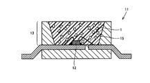
発光素子として、450nmにピーク波長を有する窒化ガリウム(GaN)系半導体を用いた。波長変換部には、Eu0.05Si11.55Al0.45O0.35N15.65(β型SiAlON)なる組成を有する緑色系発光蛍光体であり、平均粒度(d1)が11.3μm、メディアン径(50%D)が18.6μm、50%D/d1=1.65、600nmにおける吸収率が5.9%である特性値を有するものを用いた。なお、この蛍光体は主として、Al濃度(c)を0.50に制御することによって、調製されたものである。この蛍光体を、所定の割合にて媒質としての熱硬化型のシリコーン樹脂製の封止材中に分散させて分散し、発光素子を封止して、波長変換部を作製し、実施例1の発光装置を作製した。このようにして作製した実施例1の発光装置について、初期および5000時間後の明るさを測定した。なお、明るさは順電流(IF)30mAにて点灯し、発光装置からの光出力(光電流)を測定した。 Example 1, Comparative Example 1
As a light emitting element, a gallium nitride (GaN) based semiconductor having a peak wavelength of 450 nm was used. The wavelength conversion part is a green light emitting phosphor having a composition of Eu 0.05 Si 11.55 Al 0.45 O 0.35 N 15.65 (β-type SiAlON), and the average particle size (d1) is 11.3 μm, and the median diameter (50% D) Of 18.6 μm, 50% D /
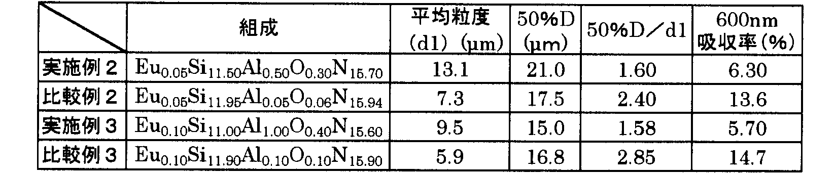
表2に示すような種々の平均粒度(d1)、メディアン径(50%D)、50%D/d1値、600nmにおける吸収率を有する蛍光体を用いたこと以外は実施例1と同様にして、それぞれ実施例2、3、比較例2、3の発光装置を作製した。実施例1と同様にして測定した特性(明るさ)の結果を表3に示す。表3から、実施例2、3の発光装置は、比較例2、3の発光装置に比し、著しく明るくかつ明るさの変動が小さいことが分かる。 <Examples 2, 3 and Comparative Examples 2, 3>
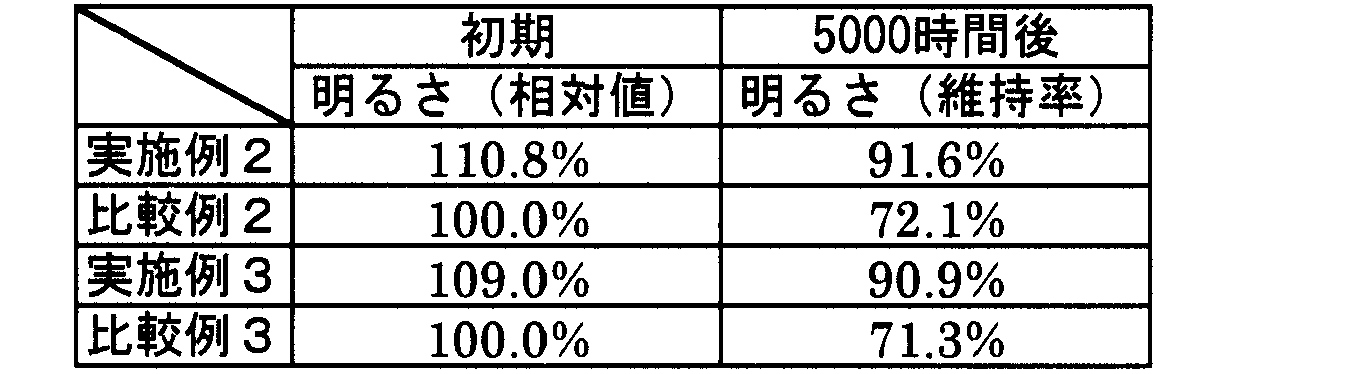
In the same manner as in Example 1 except that phosphors having various average particle sizes (d1), median diameters (50% D), 50% D / d1 values, and absorbances at 600 nm as shown in Table 2 were used. The light emitting devices of Examples 2 and 3 and Comparative Examples 2 and 3 were produced. The results of the characteristics (brightness) measured in the same manner as in Example 1 are shown in Table 3. It can be seen from Table 3 that the light emitting devices of Examples 2 and 3 are significantly brighter and have less variation in brightness than the light emitting devices of Comparative Examples 2 and 3.
発光素子として、460nmにピーク波長を有する窒化ガリウム(GaN)系半導体を用いた。波長変換部には、Eu0.05Si11.55Al0.45O0.35N15.65(β型SiAlON)なる組成を有する緑色系発光蛍光体であり、平均粒度(d1)が11.3μm、メディアン径(50%D)が18.6μm、50%D/d1=1.65、600nmにおける吸収率が5.9%である特性値を有するものと、(Ca0.99Eu0.01)AlSiN3(D50値:12.8μm)なる組成を有する2価のユーロピウム付活窒化物赤色系発光蛍光体とを用いた。この蛍光体および赤色系発光蛍光体を、所定の割合にて媒質としての熱硬化型のシリコーン樹脂製の封止材中に分散させて分散し、発光素子を封止して、波長変換部を作製し、実施例4の発光装置を作製した。このようにして作製した実施例4の発光装置について、初期および5000時間後の明るさおよび色度を測定した。なお、明るさは順電流(IF)30mAにて点灯し、発光装置からの光出力(光電流)を測定し、色度はMCPD-2000(大塚電子製)を用い、測定した。 Example 4, Comparative Example 4
As a light emitting element, a gallium nitride (GaN) based semiconductor having a peak wavelength at 460 nm was used. The wavelength conversion part is a green light emitting phosphor having a composition of Eu 0.05 Si 11.55 Al 0.45 O 0.35 N 15.65 (β-type SiAlON), and the average particle size (d1) is 11.3 μm, and the median diameter (50% D) With a characteristic value of 18.6 μm, 50% D /
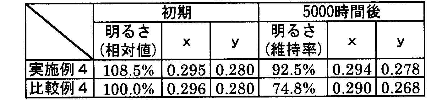
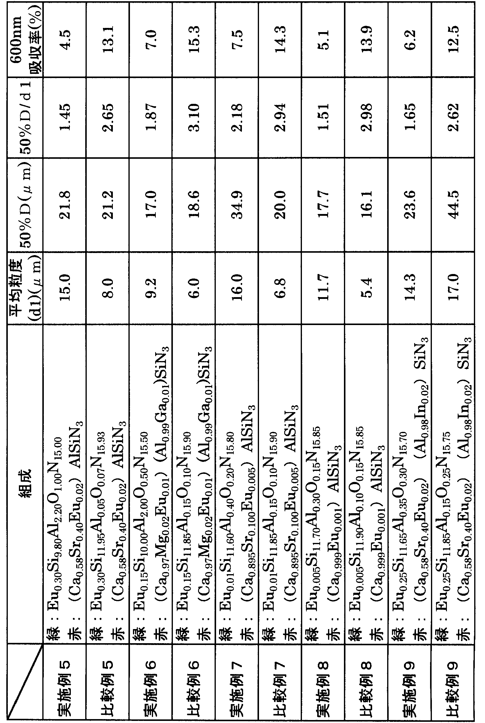
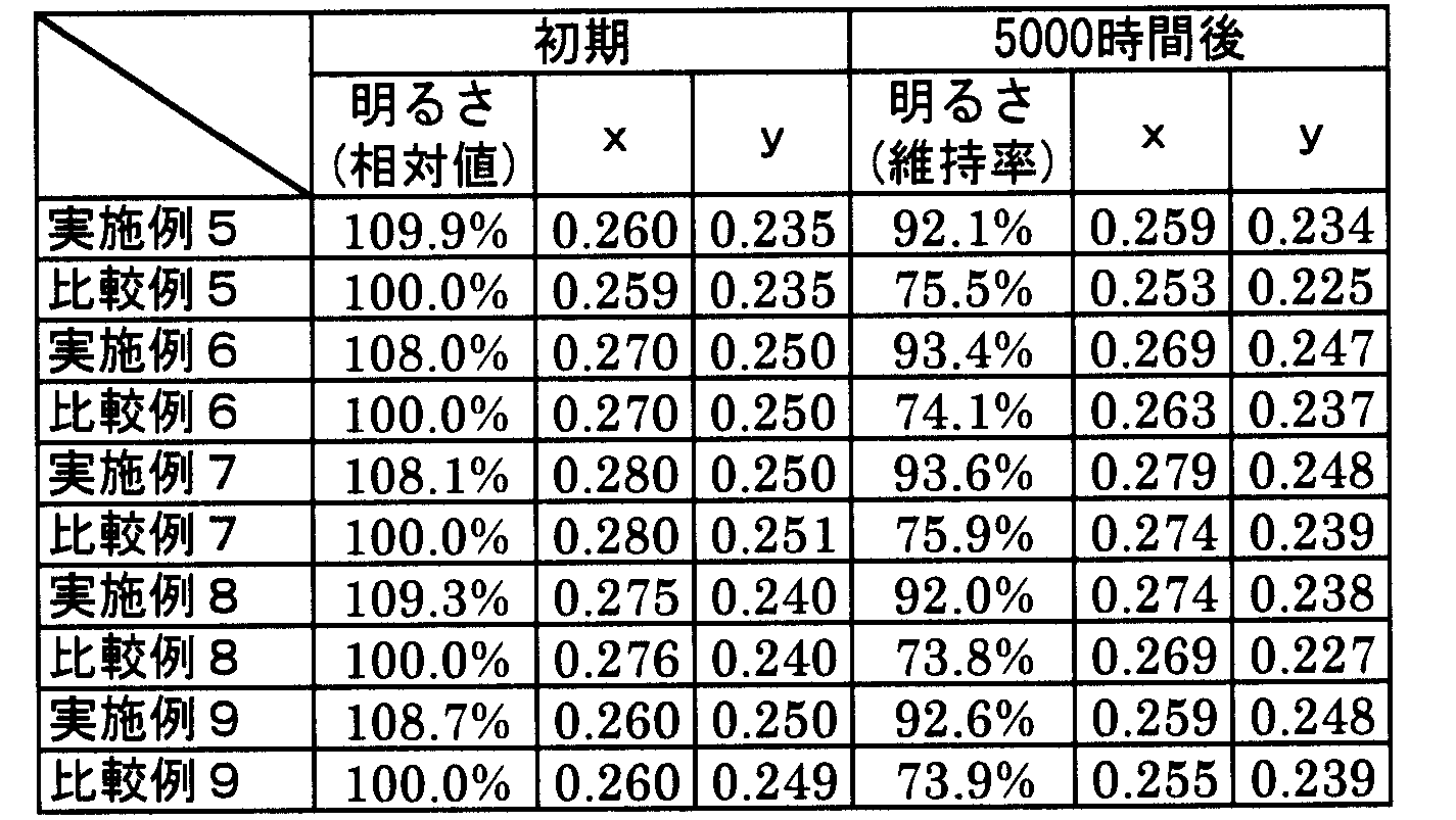
表5に示すような種々の平均粒度(d1)、メディアン径(50%D)、50%D/d1値、600nmにおける吸収率を有するβ型SiAlON蛍光体を用いたこと以外は実施例4と同様にして、それぞれ実施例5~9、比較例5~9の発光装置を作製した。実施例4と同様にして測定した特性(明るさおよび色度)の評価結果を表6に示す。表6から、実施例5~9の発光装置は、比較例5~9の発光装置に比し、著しく明るく、かつ明るさおよび色度の変動が小さいことが分かる。 Examples 5 to 9 and Comparative Examples 5 to 9
Example 4 and Example 4 were used except that β-type SiAlON phosphors having various average particle sizes (d1), median diameters (50% D), 50% D /
Claims (12)
- 一般式(A):EuaSibAlcOdNe
(一般式(A)中、0.005≦a≦0.4、b+c=12、d+e=16を満足する数である。)
で実質的に表され、平均粒度(d1)(空気透過法)が9~16μmであり、粒度分布でのメディアン径(50%D)が12.5~35μmであり、50%D/d1=1.4~2.2であり、かつ600nmにおける吸収率が8.0%以下であるβ型SiAlONである、2価のユーロピウム付活酸窒化物緑色系発光蛍光体。 General formula (A): Eu a Si b Al c O d N e
(In general formula (A), it is a number satisfying 0.005 ≦ a ≦ 0.4, b + c = 12, and d + e = 16.)
With an average particle size (d1) (air permeation method) of 9 to 16 μm, a median diameter (50% D) in the particle size distribution of 12.5 to 35 μm, 50% D / d1 = A divalent europium-activated oxynitride green light-emitting phosphor, which is a β-type SiAlON of 1.4 to 2.2 and having an absorption of not more than 8.0% at 600 nm. - 10μm≦d1≦13μm、50%D/d1=1.6~2.0かつ600nmにおける吸収率が7.0%以下である、請求項1に記載の蛍光体。 2. The phosphor according to claim 1, wherein the absorptivity at 10 μm ≦ d1 ≦ 13 μm, 50% D / d1 = 1.6 to 2.0 and 600 nm is 7.0% or less.
- 一般式(A)中、c≧0.3である、請求項1に記載の蛍光体。 The phosphor according to claim 1, wherein c ≧ 0.3 in the general formula (A).
- 一般式(A)中、0.01≦a≦0.2である、請求項1に記載の蛍光体。 The phosphor according to claim 1, wherein in the general formula (A), 0.01 ≦ a ≦ 0.2.
- ピーク波長が430~480nmの一次光を発する窒化ガリウム系半導体である発光素子と、前記一次光の一部を吸収して、一次光の波長よりも長い波長を有する二次光を発する波長変換部とを備えた発光装置であって、前記波長変換部は、
一般式(A):EuaSibAlcOdNe
(一般式(A)中、0.005≦a≦0.4、b+c=12、d+e=16を満足する数である。)
で実質的に表され、平均粒度(d1)(空気透過法)が9~16μmであり、粒度分布でのメディアン径(50%D)が12.5~35μmであり、50%D/d1=1.4~2.2であり、かつ600nmにおける吸収率が8.0%以下であるβ型SiAlONである、2価のユーロピウム付活酸窒化物緑色系発光蛍光体を含む、発光装置。 A light emitting element that is a gallium nitride based semiconductor that emits primary light with a peak wavelength of 430 to 480 nm, and a wavelength conversion unit that absorbs part of the primary light and emits secondary light having a wavelength longer than that of primary light. And the wavelength converter includes:
General formula (A): Eu a Si b Al c O d N e
(In general formula (A), it is a number satisfying 0.005 ≦ a ≦ 0.4, b + c = 12, and d + e = 16.)
With an average particle size (d1) (air permeation method) of 9 to 16 μm, a median diameter (50% D) in the particle size distribution of 12.5 to 35 μm, 50% D / d1 = A light emitting device comprising a divalent europium-activated oxynitride green light emitting phosphor which is β-type SiAlON of 1.4 to 2.2 and having an absorptivity of 8.0% or less at 600 nm. - 蛍光体が、10μm≦d1≦13μm、50%D/d1=1.6~2.0かつ600nmにおける吸収率が7.0%以下である、請求項5に記載の発光装置。 6. The light emitting device according to claim 5, wherein the phosphor has an absorption of 7.0% or less at 10 μm ≦ d1 ≦ 13 μm, 50% D / d1 = 1.6 to 2.0 and 600 nm.
- 一般式(A)中、c≧0.3である、請求項5に記載の発光装置。 The light emitting device according to claim 5, wherein in the general formula (A), c) 0.3.
- 一般式(A)中、0.01≦a≦0.2である、請求項5に記載の発光装置。 The light emitting device according to claim 5, wherein in the general formula (A), 0.01 ≦ a ≦ 0.2.
- 一般式(B):(MI1-xEux)MIISiN3
(一般式(B)中、MIはMg、Ca、SrおよびBaから選ばれる少なくとも1種のアルカリ土類金属元素を示し、MIIはAl、Ga、In、Sc、Y、La、GdおよびLuから選ばれる少なくとも1種の3価の金属元素を示し、0.001≦x≦0.10を満足する数である。)
で実質的に表される2価のユーロピウム付活窒化物赤色系発光蛍光体を波長変換部に含む、請求項5に記載の発光装置。 General formula (B): (MI 1-x Eu x ) MIISiN 3
(In the general formula (B), MI represents at least one alkaline earth metal element selected from Mg, Ca, Sr and Ba, and MII is selected from Al, Ga, In, Sc, Y, La, Gd and Lu Indicates at least one trivalent metal element to be selected, and is a number satisfying 0.001 ≦ x ≦ 0.10.
The light emitting device according to claim 5, wherein the wavelength conversion portion includes the divalent europium activated nitride red light emitting phosphor substantially represented by - 一般式(B)中、MIIはAl、GaおよびInから選ばれる少なくとも1種の元素である、請求項5に記載の発光装置。 The light emitting device according to claim 5, wherein in the general formula (B), MII is at least one element selected from Al, Ga and In.
- 請求項5に記載の発光装置を点光源として複数含むバックライト光源装置。 A backlight source device comprising a plurality of the light emitting devices according to claim 5 as point light sources.
- 液晶パネルと、
液晶パネルの背面に配置された請求項11に記載のバックライト光源装置とを備える、液晶表示装置。 LCD panel,
The liquid crystal display device provided with the backlight light source device of Claim 11 arrange | positioned at the back surface of a liquid crystal panel.
Priority Applications (7)
| Application Number | Priority Date | Filing Date | Title |
|---|---|---|---|
| EP10842184.3A EP2468836A4 (en) | 2010-01-08 | 2010-12-16 | Phosphor, light-emitting device, and liquid crystal display device using same |
| JP2011548943A JP5589002B2 (en) | 2010-01-08 | 2010-12-16 | Phosphor, light emitting device, and liquid crystal display device using the same |
| US13/500,803 US8709283B2 (en) | 2010-01-08 | 2010-12-16 | Phosphor, light emitting apparatus, and liquid crystal display apparatus using the same |
| BR112012016731A BR112012016731A2 (en) | 2010-01-08 | 2010-12-16 | "phosphorus, light-emitting apparatus and liquid crystal display apparatus using the same" |
| KR1020127006888A KR101378813B1 (en) | 2010-01-08 | 2010-12-16 | Phosphor, Light Emitting Apparatus, and Liquid Crystal Display Apparatus Using the Same |
| CN201080054430.1A CN102656248B (en) | 2010-01-08 | 2010-12-16 | Phosphor, light-emitting device, and liquid crystal display device using same |
| US14/248,664 US9496463B2 (en) | 2010-01-08 | 2014-04-09 | Phosphor, light emitting apparatus, and liquid crystal display apparatus using the same |
Applications Claiming Priority (2)
| Application Number | Priority Date | Filing Date | Title |
|---|---|---|---|
| JP2010-003058 | 2010-01-08 | ||
| JP2010003058 | 2010-01-08 |
Related Child Applications (2)
| Application Number | Title | Priority Date | Filing Date |
|---|---|---|---|
| US13/500,803 A-371-Of-International US8709283B2 (en) | 2010-01-08 | 2010-12-16 | Phosphor, light emitting apparatus, and liquid crystal display apparatus using the same |
| US14/248,664 Continuation US9496463B2 (en) | 2010-01-08 | 2014-04-09 | Phosphor, light emitting apparatus, and liquid crystal display apparatus using the same |
Publications (1)
| Publication Number | Publication Date |
|---|---|
| WO2011083671A1 true WO2011083671A1 (en) | 2011-07-14 |
Family
ID=44305408
Family Applications (1)
| Application Number | Title | Priority Date | Filing Date |
|---|---|---|---|
| PCT/JP2010/072684 WO2011083671A1 (en) | 2010-01-08 | 2010-12-16 | Phosphor, light-emitting device, and liquid crystal display device using same |
Country Status (8)
| Country | Link |
|---|---|
| US (2) | US8709283B2 (en) |
| EP (1) | EP2468836A4 (en) |
| JP (2) | JP5589002B2 (en) |
| KR (1) | KR101378813B1 (en) |
| CN (1) | CN102656248B (en) |
| BR (1) | BR112012016731A2 (en) |
| TW (1) | TWI468495B (en) |
| WO (1) | WO2011083671A1 (en) |
Cited By (5)
| Publication number | Priority date | Publication date | Assignee | Title |
|---|---|---|---|---|
| JP2013163738A (en) * | 2012-02-09 | 2013-08-22 | Denki Kagaku Kogyo Kk | Phosphor and light-emitting device |
| JP2013163721A (en) * | 2012-02-09 | 2013-08-22 | Denki Kagaku Kogyo Kk | Phosphor and light-emitting device |
| JP2013163720A (en) * | 2012-02-09 | 2013-08-22 | Denki Kagaku Kogyo Kk | Phosphor and light-emitting device |
| WO2017122800A1 (en) * | 2016-01-15 | 2017-07-20 | デンカ株式会社 | Phosphor and light emitting device |
| KR20220002390A (en) | 2019-04-23 | 2022-01-06 | 덴카 주식회사 | Phosphor powder and light emitting device |
Families Citing this family (6)
| Publication number | Priority date | Publication date | Assignee | Title |
|---|---|---|---|---|
| JP5367218B2 (en) | 2006-11-24 | 2013-12-11 | シャープ株式会社 | Method for manufacturing phosphor and method for manufacturing light emitting device |
| US8237348B2 (en) | 2008-03-03 | 2012-08-07 | Sharp Kabushiki Kaisha | Light-emitting device |
| KR101378813B1 (en) * | 2010-01-08 | 2014-03-27 | 샤프 가부시키가이샤 | Phosphor, Light Emitting Apparatus, and Liquid Crystal Display Apparatus Using the Same |
| WO2014091776A1 (en) * | 2012-12-14 | 2014-06-19 | 電気化学工業株式会社 | Phosphor, method for producing same, and light emitting device |
| KR102353443B1 (en) | 2014-12-22 | 2022-01-21 | 삼성전자주식회사 | Oxynitride-based phosphor and white light emitting device including the same |
| EP3669115B1 (en) * | 2017-08-18 | 2023-10-04 | Thorlabs, Inc. | Broadband light source based on crystalline phosphor |
Citations (4)
| Publication number | Priority date | Publication date | Assignee | Title |
|---|---|---|---|---|
| WO2007129713A1 (en) * | 2006-05-10 | 2007-11-15 | Denki Kagaku Kogyo Kabushiki Kaisha | Sialon phosphor, process for producing the same, and illuminator and luminescent element employing the same |
| JP2007308593A (en) * | 2006-05-18 | 2007-11-29 | Denki Kagaku Kogyo Kk | Process for production of sialon fluorescent material, sialon fluorescent material and fluorescent light assembly |
| WO2008062781A1 (en) * | 2006-11-20 | 2008-05-29 | Denki Kagaku Kogyo Kabushiki Kaisha | Fluorescent substance and production method thereof, and light emitting device |
| WO2009008250A1 (en) * | 2007-07-09 | 2009-01-15 | Sharp Kabushiki Kaisha | Group of phosphor particles, and light-emitting device using the same |
Family Cites Families (20)
| Publication number | Priority date | Publication date | Assignee | Title |
|---|---|---|---|---|
| US6608332B2 (en) | 1996-07-29 | 2003-08-19 | Nichia Kagaku Kogyo Kabushiki Kaisha | Light emitting device and display |
| TW383508B (en) | 1996-07-29 | 2000-03-01 | Nichia Kagaku Kogyo Kk | Light emitting device and display |
| JP3609709B2 (en) | 2000-09-29 | 2005-01-12 | 株式会社シチズン電子 | Light emitting diode |
| CN100405620C (en) | 2002-06-13 | 2008-07-23 | 美商克立股份有限公司 | Saturated phosphor solid state emitter |
| KR100609830B1 (en) | 2003-04-25 | 2006-08-09 | 럭스피아 주식회사 | White Semiconductor Light Emitted Device using Green-emitting and Red emitting Phosphor |
| JP3921545B2 (en) | 2004-03-12 | 2007-05-30 | 独立行政法人物質・材料研究機構 | Phosphor and production method thereof |
| JP4517783B2 (en) | 2004-08-31 | 2010-08-04 | 日亜化学工業株式会社 | Rare earth boroaluminate phosphor and light emitting device using the same |
| JP5086641B2 (en) | 2004-09-22 | 2012-11-28 | 株式会社東芝 | LIGHT EMITTING DEVICE, BACKLIGHT AND LIQUID CRYSTAL DISPLAY DEVICE USING THE SAME |
| JP4934792B2 (en) * | 2005-08-04 | 2012-05-16 | Dowaエレクトロニクス株式会社 | Phosphor, method for producing the same, and light emitting device using the phosphor |
| EP2463354B1 (en) * | 2005-12-08 | 2017-03-29 | National Institute for Materials Science | Phosphor, Process for producing the same, and luminescent device |
| EP1985683B1 (en) | 2006-02-02 | 2013-08-28 | Mitsubishi Chemical Corporation | Complex oxynitride phosphor, light-emitting device using same, image display, illuminating device, phosphor-containing composition and complex oxynitride |
| KR101354896B1 (en) * | 2006-07-05 | 2014-01-24 | 우베 고산 가부시키가이샤 | Sialon-base oxynitride phosphors and process for production thereof |
| JP2008120938A (en) * | 2006-11-14 | 2008-05-29 | Sharp Corp | Phosphor, its manufacturing method, semiconductor light emitting device and image display device |
| JP5367218B2 (en) | 2006-11-24 | 2013-12-11 | シャープ株式会社 | Method for manufacturing phosphor and method for manufacturing light emitting device |
| JP2009019163A (en) * | 2007-07-13 | 2009-01-29 | Sharp Corp | Phosphor particle aggregate for light emitting device, light emitting device, and backlight device for liquid crystal display |
| JP2009092253A (en) | 2007-10-04 | 2009-04-30 | Masaji Furukawa | Double chimney combustion appliance |
| CN101821356B (en) * | 2007-10-10 | 2013-11-06 | 宇部兴产株式会社 | [beta]-sialon phosphor powder and process for production of the same |
| JP2009167338A (en) * | 2008-01-18 | 2009-07-30 | Sharp Corp | Wavelength conversion member, light emitting device having it, and phosphor |
| KR101378813B1 (en) * | 2010-01-08 | 2014-03-27 | 샤프 가부시키가이샤 | Phosphor, Light Emitting Apparatus, and Liquid Crystal Display Apparatus Using the Same |
| JP4740379B1 (en) | 2010-02-25 | 2011-08-03 | 電気化学工業株式会社 | β-type sialon phosphor, its use and method for producing β-type sialon phosphor |
-
2010
- 2010-12-16 KR KR1020127006888A patent/KR101378813B1/en active IP Right Grant
- 2010-12-16 JP JP2011548943A patent/JP5589002B2/en active Active
- 2010-12-16 CN CN201080054430.1A patent/CN102656248B/en active Active
- 2010-12-16 BR BR112012016731A patent/BR112012016731A2/en not_active Application Discontinuation
- 2010-12-16 WO PCT/JP2010/072684 patent/WO2011083671A1/en active Application Filing
- 2010-12-16 US US13/500,803 patent/US8709283B2/en active Active
- 2010-12-16 EP EP10842184.3A patent/EP2468836A4/en not_active Ceased
- 2010-12-27 TW TW99146167A patent/TWI468495B/en active
-
2014
- 2014-04-09 US US14/248,664 patent/US9496463B2/en active Active
- 2014-07-22 JP JP2014149016A patent/JP2014209660A/en active Pending
Patent Citations (4)
| Publication number | Priority date | Publication date | Assignee | Title |
|---|---|---|---|---|
| WO2007129713A1 (en) * | 2006-05-10 | 2007-11-15 | Denki Kagaku Kogyo Kabushiki Kaisha | Sialon phosphor, process for producing the same, and illuminator and luminescent element employing the same |
| JP2007308593A (en) * | 2006-05-18 | 2007-11-29 | Denki Kagaku Kogyo Kk | Process for production of sialon fluorescent material, sialon fluorescent material and fluorescent light assembly |
| WO2008062781A1 (en) * | 2006-11-20 | 2008-05-29 | Denki Kagaku Kogyo Kabushiki Kaisha | Fluorescent substance and production method thereof, and light emitting device |
| WO2009008250A1 (en) * | 2007-07-09 | 2009-01-15 | Sharp Kabushiki Kaisha | Group of phosphor particles, and light-emitting device using the same |
Non-Patent Citations (1)
| Title |
|---|
| See also references of EP2468836A4 * |
Cited By (8)
| Publication number | Priority date | Publication date | Assignee | Title |
|---|---|---|---|---|
| JP2013163738A (en) * | 2012-02-09 | 2013-08-22 | Denki Kagaku Kogyo Kk | Phosphor and light-emitting device |
| JP2013163721A (en) * | 2012-02-09 | 2013-08-22 | Denki Kagaku Kogyo Kk | Phosphor and light-emitting device |
| JP2013163720A (en) * | 2012-02-09 | 2013-08-22 | Denki Kagaku Kogyo Kk | Phosphor and light-emitting device |
| WO2017122800A1 (en) * | 2016-01-15 | 2017-07-20 | デンカ株式会社 | Phosphor and light emitting device |
| JPWO2017122800A1 (en) * | 2016-01-15 | 2018-11-08 | デンカ株式会社 | Phosphor and light emitting device |
| JP7045192B2 (en) | 2016-01-15 | 2022-03-31 | デンカ株式会社 | Fluorescent material and light emitting device |
| KR20220002390A (en) | 2019-04-23 | 2022-01-06 | 덴카 주식회사 | Phosphor powder and light emitting device |
| US11781064B2 (en) | 2019-04-23 | 2023-10-10 | Denka Company Limited | Phosphor powder and light-emitting device |
Also Published As
| Publication number | Publication date |
|---|---|
| KR101378813B1 (en) | 2014-03-27 |
| BR112012016731A2 (en) | 2018-05-15 |
| US8709283B2 (en) | 2014-04-29 |
| JP2014209660A (en) | 2014-11-06 |
| TWI468495B (en) | 2015-01-11 |
| CN102656248B (en) | 2014-07-16 |
| EP2468836A1 (en) | 2012-06-27 |
| TW201134922A (en) | 2011-10-16 |
| US9496463B2 (en) | 2016-11-15 |
| JPWO2011083671A1 (en) | 2013-05-13 |
| US20120194762A1 (en) | 2012-08-02 |
| EP2468836A4 (en) | 2014-07-30 |
| JP5589002B2 (en) | 2014-09-10 |
| CN102656248A (en) | 2012-09-05 |
| KR20120048020A (en) | 2012-05-14 |
| US20140218658A1 (en) | 2014-08-07 |
Similar Documents
| Publication | Publication Date | Title |
|---|---|---|
| WO2011083671A1 (en) | Phosphor, light-emitting device, and liquid crystal display device using same | |
| US10259997B2 (en) | Phosphor, method of producing the same, and light emitting apparatus | |
| US9356203B2 (en) | Phosphor particle group and light emitting apparatus using the same | |
| JP4769132B2 (en) | Light emitting device | |
| WO2009110285A1 (en) | Light-emitting device | |
| US20110279016A1 (en) | Carbonitride based phosphors and light emitting devices using the same | |
| JP2009280763A (en) | Phosphor preparation and light emitting device using it | |
| JP2007191680A (en) | Light-emitting device | |
| KR101250838B1 (en) | Group of phosphor particles, light-emitting device using same, and liquid crystal television receiver | |
| JP2018113411A (en) | Light-emitting device | |
| JP2009076656A (en) | Light emitting device, image display device and liquid crystal display | |
| JP2013227527A (en) | Phosphor and light emitting device using the same | |
| JP2011091414A (en) | Light-emitting device |
Legal Events
| Date | Code | Title | Description |
|---|---|---|---|
| WWE | Wipo information: entry into national phase |
Ref document number: 201080054430.1 Country of ref document: CN |
|
| 121 | Ep: the epo has been informed by wipo that ep was designated in this application |
Ref document number: 10842184 Country of ref document: EP Kind code of ref document: A1 |
|
| WWE | Wipo information: entry into national phase |
Ref document number: 2011548943 Country of ref document: JP |
|
| ENP | Entry into the national phase |
Ref document number: 20127006888 Country of ref document: KR Kind code of ref document: A |
|
| WWE | Wipo information: entry into national phase |
Ref document number: 2010842184 Country of ref document: EP |
|
| WWE | Wipo information: entry into national phase |
Ref document number: 13500803 Country of ref document: US |
|
| NENP | Non-entry into the national phase |
Ref country code: DE |
|
| WWE | Wipo information: entry into national phase |
Ref document number: 6844/CHENP/2012 Country of ref document: IN |
|
| REG | Reference to national code |
Ref country code: BR Ref legal event code: B01A Ref document number: 112012016731 Country of ref document: BR |
|
| ENP | Entry into the national phase |
Ref document number: 112012016731 Country of ref document: BR Kind code of ref document: A2 Effective date: 20120706 |