KR20120048020A - Phosphor, light-emitting device, and liquid crystal display device using same - Google Patents
Phosphor, light-emitting device, and liquid crystal display device using same Download PDFInfo
- Publication number
- KR20120048020A KR20120048020A KR1020127006888A KR20127006888A KR20120048020A KR 20120048020 A KR20120048020 A KR 20120048020A KR 1020127006888 A KR1020127006888 A KR 1020127006888A KR 20127006888 A KR20127006888 A KR 20127006888A KR 20120048020 A KR20120048020 A KR 20120048020A
- Authority
- KR
- South Korea
- Prior art keywords
- light emitting
- light
- phosphor
- emitting device
- general formula
- Prior art date
Links
Images

Classifications
-
- H—ELECTRICITY
- H01—ELECTRIC ELEMENTS
- H01L—SEMICONDUCTOR DEVICES NOT COVERED BY CLASS H10
- H01L33/00—Semiconductor devices with at least one potential-jump barrier or surface barrier specially adapted for light emission; Processes or apparatus specially adapted for the manufacture or treatment thereof or of parts thereof; Details thereof
- H01L33/48—Semiconductor devices with at least one potential-jump barrier or surface barrier specially adapted for light emission; Processes or apparatus specially adapted for the manufacture or treatment thereof or of parts thereof; Details thereof characterised by the semiconductor body packages
- H01L33/50—Wavelength conversion elements
- H01L33/501—Wavelength conversion elements characterised by the materials, e.g. binder
- H01L33/502—Wavelength conversion materials
- H01L33/504—Elements with two or more wavelength conversion materials
-
- C—CHEMISTRY; METALLURGY
- C09—DYES; PAINTS; POLISHES; NATURAL RESINS; ADHESIVES; COMPOSITIONS NOT OTHERWISE PROVIDED FOR; APPLICATIONS OF MATERIALS NOT OTHERWISE PROVIDED FOR
- C09K—MATERIALS FOR MISCELLANEOUS APPLICATIONS, NOT PROVIDED FOR ELSEWHERE
- C09K11/00—Luminescent, e.g. electroluminescent, chemiluminescent materials
- C09K11/08—Luminescent, e.g. electroluminescent, chemiluminescent materials containing inorganic luminescent materials
- C09K11/64—Luminescent, e.g. electroluminescent, chemiluminescent materials containing inorganic luminescent materials containing aluminium
-
- C—CHEMISTRY; METALLURGY
- C09—DYES; PAINTS; POLISHES; NATURAL RESINS; ADHESIVES; COMPOSITIONS NOT OTHERWISE PROVIDED FOR; APPLICATIONS OF MATERIALS NOT OTHERWISE PROVIDED FOR
- C09K—MATERIALS FOR MISCELLANEOUS APPLICATIONS, NOT PROVIDED FOR ELSEWHERE
- C09K11/00—Luminescent, e.g. electroluminescent, chemiluminescent materials
- C09K11/08—Luminescent, e.g. electroluminescent, chemiluminescent materials containing inorganic luminescent materials
- C09K11/0883—Arsenides; Nitrides; Phosphides
-
- C—CHEMISTRY; METALLURGY
- C09—DYES; PAINTS; POLISHES; NATURAL RESINS; ADHESIVES; COMPOSITIONS NOT OTHERWISE PROVIDED FOR; APPLICATIONS OF MATERIALS NOT OTHERWISE PROVIDED FOR
- C09K—MATERIALS FOR MISCELLANEOUS APPLICATIONS, NOT PROVIDED FOR ELSEWHERE
- C09K11/00—Luminescent, e.g. electroluminescent, chemiluminescent materials
- C09K11/08—Luminescent, e.g. electroluminescent, chemiluminescent materials containing inorganic luminescent materials
- C09K11/59—Luminescent, e.g. electroluminescent, chemiluminescent materials containing inorganic luminescent materials containing silicon
-
- C—CHEMISTRY; METALLURGY
- C09—DYES; PAINTS; POLISHES; NATURAL RESINS; ADHESIVES; COMPOSITIONS NOT OTHERWISE PROVIDED FOR; APPLICATIONS OF MATERIALS NOT OTHERWISE PROVIDED FOR
- C09K—MATERIALS FOR MISCELLANEOUS APPLICATIONS, NOT PROVIDED FOR ELSEWHERE
- C09K11/00—Luminescent, e.g. electroluminescent, chemiluminescent materials
- C09K11/08—Luminescent, e.g. electroluminescent, chemiluminescent materials containing inorganic luminescent materials
- C09K11/77—Luminescent, e.g. electroluminescent, chemiluminescent materials containing inorganic luminescent materials containing rare earth metals
- C09K11/7728—Luminescent, e.g. electroluminescent, chemiluminescent materials containing inorganic luminescent materials containing rare earth metals containing europium
- C09K11/77348—Silicon Aluminium Nitrides or Silicon Aluminium Oxynitrides
-
- G—PHYSICS
- G02—OPTICS
- G02F—OPTICAL DEVICES OR ARRANGEMENTS FOR THE CONTROL OF LIGHT BY MODIFICATION OF THE OPTICAL PROPERTIES OF THE MEDIA OF THE ELEMENTS INVOLVED THEREIN; NON-LINEAR OPTICS; FREQUENCY-CHANGING OF LIGHT; OPTICAL LOGIC ELEMENTS; OPTICAL ANALOGUE/DIGITAL CONVERTERS
- G02F1/00—Devices or arrangements for the control of the intensity, colour, phase, polarisation or direction of light arriving from an independent light source, e.g. switching, gating or modulating; Non-linear optics
- G02F1/01—Devices or arrangements for the control of the intensity, colour, phase, polarisation or direction of light arriving from an independent light source, e.g. switching, gating or modulating; Non-linear optics for the control of the intensity, phase, polarisation or colour
- G02F1/13—Devices or arrangements for the control of the intensity, colour, phase, polarisation or direction of light arriving from an independent light source, e.g. switching, gating or modulating; Non-linear optics for the control of the intensity, phase, polarisation or colour based on liquid crystals, e.g. single liquid crystal display cells
- G02F1/133—Constructional arrangements; Operation of liquid crystal cells; Circuit arrangements
- G02F1/1333—Constructional arrangements; Manufacturing methods
- G02F1/1335—Structural association of cells with optical devices, e.g. polarisers or reflectors
- G02F1/1336—Illuminating devices
- G02F1/133602—Direct backlight
- G02F1/133603—Direct backlight with LEDs
-
- H—ELECTRICITY
- H01—ELECTRIC ELEMENTS
- H01L—SEMICONDUCTOR DEVICES NOT COVERED BY CLASS H10
- H01L33/00—Semiconductor devices with at least one potential-jump barrier or surface barrier specially adapted for light emission; Processes or apparatus specially adapted for the manufacture or treatment thereof or of parts thereof; Details thereof
- H01L33/48—Semiconductor devices with at least one potential-jump barrier or surface barrier specially adapted for light emission; Processes or apparatus specially adapted for the manufacture or treatment thereof or of parts thereof; Details thereof characterised by the semiconductor body packages
- H01L33/50—Wavelength conversion elements
- H01L33/501—Wavelength conversion elements characterised by the materials, e.g. binder
- H01L33/502—Wavelength conversion materials
-
- H—ELECTRICITY
- H01—ELECTRIC ELEMENTS
- H01L—SEMICONDUCTOR DEVICES NOT COVERED BY CLASS H10
- H01L2224/00—Indexing scheme for arrangements for connecting or disconnecting semiconductor or solid-state bodies and methods related thereto as covered by H01L24/00
- H01L2224/01—Means for bonding being attached to, or being formed on, the surface to be connected, e.g. chip-to-package, die-attach, "first-level" interconnects; Manufacturing methods related thereto
- H01L2224/42—Wire connectors; Manufacturing methods related thereto
- H01L2224/47—Structure, shape, material or disposition of the wire connectors after the connecting process
- H01L2224/48—Structure, shape, material or disposition of the wire connectors after the connecting process of an individual wire connector
- H01L2224/4805—Shape
- H01L2224/4809—Loop shape
- H01L2224/48091—Arched
-
- H—ELECTRICITY
- H01—ELECTRIC ELEMENTS
- H01L—SEMICONDUCTOR DEVICES NOT COVERED BY CLASS H10
- H01L2224/00—Indexing scheme for arrangements for connecting or disconnecting semiconductor or solid-state bodies and methods related thereto as covered by H01L24/00
- H01L2224/01—Means for bonding being attached to, or being formed on, the surface to be connected, e.g. chip-to-package, die-attach, "first-level" interconnects; Manufacturing methods related thereto
- H01L2224/42—Wire connectors; Manufacturing methods related thereto
- H01L2224/47—Structure, shape, material or disposition of the wire connectors after the connecting process
- H01L2224/48—Structure, shape, material or disposition of the wire connectors after the connecting process of an individual wire connector
- H01L2224/481—Disposition
- H01L2224/48151—Connecting between a semiconductor or solid-state body and an item not being a semiconductor or solid-state body, e.g. chip-to-substrate, chip-to-passive
- H01L2224/48221—Connecting between a semiconductor or solid-state body and an item not being a semiconductor or solid-state body, e.g. chip-to-substrate, chip-to-passive the body and the item being stacked
- H01L2224/48245—Connecting between a semiconductor or solid-state body and an item not being a semiconductor or solid-state body, e.g. chip-to-substrate, chip-to-passive the body and the item being stacked the item being metallic
- H01L2224/48247—Connecting between a semiconductor or solid-state body and an item not being a semiconductor or solid-state body, e.g. chip-to-substrate, chip-to-passive the body and the item being stacked the item being metallic connecting the wire to a bond pad of the item
-
- H—ELECTRICITY
- H01—ELECTRIC ELEMENTS
- H01L—SEMICONDUCTOR DEVICES NOT COVERED BY CLASS H10
- H01L2224/00—Indexing scheme for arrangements for connecting or disconnecting semiconductor or solid-state bodies and methods related thereto as covered by H01L24/00
- H01L2224/01—Means for bonding being attached to, or being formed on, the surface to be connected, e.g. chip-to-package, die-attach, "first-level" interconnects; Manufacturing methods related thereto
- H01L2224/42—Wire connectors; Manufacturing methods related thereto
- H01L2224/47—Structure, shape, material or disposition of the wire connectors after the connecting process
- H01L2224/48—Structure, shape, material or disposition of the wire connectors after the connecting process of an individual wire connector
- H01L2224/481—Disposition
- H01L2224/48151—Connecting between a semiconductor or solid-state body and an item not being a semiconductor or solid-state body, e.g. chip-to-substrate, chip-to-passive
- H01L2224/48221—Connecting between a semiconductor or solid-state body and an item not being a semiconductor or solid-state body, e.g. chip-to-substrate, chip-to-passive the body and the item being stacked
- H01L2224/48245—Connecting between a semiconductor or solid-state body and an item not being a semiconductor or solid-state body, e.g. chip-to-substrate, chip-to-passive the body and the item being stacked the item being metallic
- H01L2224/48257—Connecting between a semiconductor or solid-state body and an item not being a semiconductor or solid-state body, e.g. chip-to-substrate, chip-to-passive the body and the item being stacked the item being metallic connecting the wire to a die pad of the item
-
- Y—GENERAL TAGGING OF NEW TECHNOLOGICAL DEVELOPMENTS; GENERAL TAGGING OF CROSS-SECTIONAL TECHNOLOGIES SPANNING OVER SEVERAL SECTIONS OF THE IPC; TECHNICAL SUBJECTS COVERED BY FORMER USPC CROSS-REFERENCE ART COLLECTIONS [XRACs] AND DIGESTS
- Y10—TECHNICAL SUBJECTS COVERED BY FORMER USPC
- Y10T—TECHNICAL SUBJECTS COVERED BY FORMER US CLASSIFICATION
- Y10T428/00—Stock material or miscellaneous articles
- Y10T428/29—Coated or structually defined flake, particle, cell, strand, strand portion, rod, filament, macroscopic fiber or mass thereof
- Y10T428/2982—Particulate matter [e.g., sphere, flake, etc.]
Abstract
일반식 (A) : EuaSibAlcOdNe(일반식 (A) 중 0.005≤a≤0.4, b+c=12, d+e=16을 만족하는 수이다.)로 실질적으로 표시되고, 평균 입도(d1)(공기 투과법)가 9~16μm이고, 입도 분포의 메디안 직경 (50% D)이 12.5~35μm이며, 50% D/d1=1.4~2.2이고, 또한 600nm의 흡수율이 8.0% 이하인 β형 SiAlON인, 2가의 유로퓸 활성화 산질화물 녹색계 발광 형광체, 및 그를 사용한 발광장치, BL 광원장치, 및 액정표시장치에 의해, 분산성을 제어하고, 투명성을 높인 β형 SiAlON을 사용함으로써, 고효율로 특성이 안정된 발광장치 및 그를 사용한 액정표시장치를 제공한다.General formula (A): Eu a Si b Al c O d N e (a number satisfying 0.005 ≦ a ≦ 0.4, b + c = 12, d + e = 16 in General Formula (A)). The average particle size (d1) (air permeation method) is shown, and the median diameter (50% D) of the particle size distribution is 12.5 to 35 μm, 50% D / d1 = 1.4 to 2.2, and an absorption rate of 600 nm. The β-type SiAlON which controlled dispersibility and improved transparency by the divalent europium activated oxynitride green-based fluorescent substance which is β type SiAlON which is 8.0% or less, and the light-emitting device, BL light source device, and liquid crystal display device using the same, The present invention provides a light emitting device having stable characteristics at high efficiency and a liquid crystal display device using the same.
Description
본 발명은 발광 장치용으로서 적합한 형광체 및 그를 파장 변환부에 사용한 발광 장치, 특히 특성이 안정된 발광 장치 및 그를 사용한 액정 표시 장치에 관한 것이다.BACKGROUND OF THE
반도체 발광 소자와 형광체를 조합시킨 발광 장치는, 저 소비전력, 소형, 고휘도, 광범위한 색 재현성, 및 고 연색성이 기대되는 차세대의 발광 장치로서 주목되고, 활발히 연구 개발이 행해지고 있다. 발광 소자로부터 발해지는 1차광은, 통상, 장파장의 자외선으로부터 청색의 범위, 즉, 380~480nm의 것이 사용된다. 이 용도에 적합한 다양한 형광체를 사용한 파장 변환부도 제안되어 있다.BACKGROUND ART A light emitting device in which a semiconductor light emitting element and a phosphor are combined is attracting attention as a next-generation light emitting device that is expected to have low power consumption, small size, high brightness, wide color reproducibility, and high color rendering, and is being actively researched and developed. The primary light emitted from the light emitting element is usually a long wavelength ultraviolet ray, that is, a range of 380 to 480 nm. The wavelength conversion part using the various fluorescent substance suitable for this use is also proposed.
현재, 이런 종류의 백색의 발광 장치로서는, 청색 발광의 발광 소자(피크 파장 : 460nm 전후)와 그의 청색에 의해 여기되고 황색 발광을 나타내는 3가의 세륨으로 활성화된 (Y,Gd)3(Al,Ga)5O12 형광체 또는 2가의 유로퓸으로 활성화된 2(Sr,Ba)O?SiO2 형광체와의 조합이 주로 사용되고 있다. 그러나, 이들 발광 장치에서는, 색 재현성(NTSC비)이 70% 전후이고, 최근, 소형 LCD에 있어서도 더욱 색 재현성이 양호한 것이 요구되고 있다.At present, as this type of white light emitting device, (Y, Gd) 3 (Al, Ga activated by blue light emitting element (peak wavelength: around 460 nm) and trivalent cerium excited by its blue and showing yellow light emission ) A combination with a 5 O 12 phosphor or a 2 (Sr, Ba) O? SiO 2 phosphor activated with divalent europium is mainly used. However, in these light emitting devices, the color reproducibility (NTSC ratio) is around 70%, and in recent years, it is required that the color reproducibility is good even in a small LCD.
또한, 최근 이런 종류의 발광 장치에 대해 변환 효율(밝기)뿐만 아니라, 입력 에너지를 더 높게 하고, 더 밝게 하고자 하는 시도가 행해지고 있다. 입력 에너지를 높게 한 경우, 파장 변환부를 포함한 발광 장치 전체의 효율적인 방열이 필요하게 된다. 이 때문에, 발광 장치 전체의 구조, 재질 등의 개발도 진행되고 있으나, 동작시에 있어서의 발광 소자 및 파장 변환부의 온도 상승은 피할 수 없는 것이 현실이다.In addition, in recent years, attempts have been made to make input energy higher and brighter as well as conversion efficiency (brightness) for this kind of light emitting device. When the input energy is increased, efficient heat dissipation of the entire light emitting device including the wavelength converter is required. For this reason, development of the structure, material, etc. of the whole light emitting device is also progressing, but it is the reality that the temperature rise of the light emitting element and a wavelength conversion part at the time of operation is unavoidable.
그러나, 특히 3가의 세륨으로 활성화된 (Y,Gd)3(Al,Ga)5O12 형광체에 있어서는, 25℃에서의 휘도(밝기)를 100%로 한 경우에, 100℃에서의 휘도는 85% 전후로 저하하기 때문에, 입력 에너지를 높게 설정할 수 없다고 하는 기술적 과제를 갖고 있다. 따라서, 이런 종류의 발광 장치에 대해, 사용되는 형광체의 온도 특성의 개선도 시급해 지고 있다.However, especially in the (Y, Gd) 3 (Al, Ga) 5 O 12 phosphor activated with trivalent cerium, the luminance at 100 ° C. is 85 when the luminance (brightness) at 25 ° C. is 100%. Since it falls around%, it has the technical subject that an input energy cannot be set high. Therefore, for this kind of light emitting device, there is also an urgent need to improve the temperature characteristics of the phosphors used.
이들 기술적 과제에 대해, EuaSibAlcOdNe로 표시되는 β형 SiAlON인 2가의 유로퓸 활성화 산질화물 녹색계 발광 형광체를 사용함으로써, 색 재현성(NTSC비) 및 온도 특성이 양호한 발광 장치를 얻을 수 있는 것이 알려져 있다.For these technical problems, a light emitting device having good color reproducibility (NTSC ratio) and temperature characteristics by using a divalent europium activated oxynitride green light emitting phosphor of β-type SiAlON represented by Eu a Si b Al c O d N e It is known that can be obtained.
그러나, β형 SiAlON인 2가의 유로퓸 활성화 산질화물 녹색계 발광 형광체는, 기본적으로 주상(柱狀) 결정체이고, 또한 단순한 조성상 그의 결정 구조를 유지하고자 하면, 소결체(응집체)가 생성되기 쉽다. 극단적으로 큰 주상 결정체(침상 결정체)는 결정 성장이 불충분하고, 양호한 특성(밝기)이 얻어지지 않는다. 또한, 소결체(응집체)는 균일한 1개의 입자가 아니기 때문에, 입계에서의 빛의 흡수 등에 의해, 그의 크기에도 불구하고 양호한 특성(밝기)이 얻어지지 않는다. 특히, 많은 주상 결정체(침상 결정체)나 소결체(응집체)가 존재하면, 발광 장치에 있어서 충분한 밝기를 얻을 수 없고, 또한 연속 점등 시에 있어서도 밝기의 저하 및 색도의 변동이 커진다고 하는 기술적 과제를 갖고 있다.However, bivalent europium activated oxynitride green light emitting phosphors, which are β-type SiAlON, are basically columnar crystals, and sintered bodies (aggregates) are easily formed when the crystal structure is to be maintained in a simple composition. Extremely large columnar crystals (acicular crystals) have insufficient crystal growth, and good characteristics (brightness) are not obtained. In addition, since the sintered compact (aggregate) is not a single uniform particle, good characteristics (brightness) cannot be obtained despite its size due to absorption of light at the grain boundary or the like. In particular, when there are many columnar crystals (acicular crystals) or sintered bodies (aggregates), sufficient brightness cannot be obtained in the light emitting device, and there is a technical problem that the brightness decreases and the chromaticity fluctuations increase even during continuous lighting. .
따라서, 형상을 제어한 EuaSibAlcOdNe로 표시되는 β형 SiAlON인 2가의 유로 퓸 활성화 산질화물 녹색계 발광 형광체 및 이를 사용한 특성이 안정된 발광 장치의 개발이 급선무로 되고 있다. 예를 들어, 일본국 특개 2005-255895호 공보(특허 문헌 1)에는, β형 SiAlON 관해, 결정상이, 평균 입경 50nm 이상 20μm 이하의 단결정 으로 있거나, 합성한 형광체 분말의 평균 입경을 50nm 이상 20μm 이하로 입도 조정하는 것이 기재되어 있다. 또한, 평균 입경이 20μm보다 커지면, 조명기구 및 화상 표시 장치에 적용할 때 분산성이 악화하고, 색 얼룩이 발생하기 때문에 바람직하지 않다. 50nm보다 작아지면 분말이 응집하기 때문에 조작성이 나빠지는 것도 기재되어 있다. 그러나, 특허 문헌 1에 있어서는, 분산성((응집(소결)의 정도))에 관한 기재는 없으며, 또한 그와 600nm에 있어서의 흡수율과의 관계, 그리고 발광 장치의 초기 특성 및 수명 특성에 관한 기재는 없다.Accordingly, development of a divalent europium-activated oxynitride green light-emitting phosphor of β-type SiAlON represented by Eu a Si b Al c O d N e having a shape-controlled shape and a light emitting device having stable characteristics using the same has been urgently needed. For example, Japanese Patent Laid-Open No. 2005-255895 (Patent Document 1) discloses that the β-SiAlON crystal phase has a single crystal having an average particle diameter of 50 nm or more and 20 μm or less, or the average particle diameter of the synthesized phosphor powder is 50 nm or more and 20 μm or less. It is described to adjust the particle size. In addition, when the average particle diameter is larger than 20 µm, dispersibility deteriorates and color unevenness occurs when applied to a lighting device and an image display device, which is not preferable. It is also described that operability worsens because powder aggregates when it becomes smaller than 50 nm. However, in
선행 기술 문헌Prior art literature
특허 문헌Patent Literature
특허 문헌 1 : 일본국 특개 2005-255895호 공보Patent Document 1: Japanese Patent Application Laid-Open No. 2005-255895
본 발명은 상기 과제를 해결하기 위해 한 것으로, 그 목적으로 하는 바는, 분산성을 제어하고, 투명성을 높인 β형 SiAlON을 사용함으로써, 고효율로 특성이 안정된 발광 장치를 제공하는 것이다.SUMMARY OF THE INVENTION The present invention has been made to solve the above problems, and an object thereof is to provide a light emitting device having stable characteristics with high efficiency by using a β-type SiAlON that controls dispersibility and enhances transparency.
본 발명자들은, 상기 과제를 해결하기 위해 예의 조사, 검토 및 개발을 행한 결과, β형 SiAlON의 화학 조성의 최적화에만 의존하지 않고, 한층 그 입자의 분산성을 향상시키는 것에 의해 결정의 투명성이 향상되고, 그 β형 SiAlON을 사용함으로써, 초기 특성(밝기)이 현저하게 양호하고, 또한 양호한 수명 특성을 갖는 발광 장치를 얻을 수 있는 것을 발견했다. 즉, 본 발명은 다음과 같다.MEANS TO SOLVE THE PROBLEM As a result of earnestly investigating, examining, and developing in order to solve the said subject, the transparency of a crystal | crystallization is improved by not only relying on optimization of the chemical composition of (beta) -type SiAlON, but also improving the dispersibility of the particle | grains. By using the β-type SiAlON, it was found that a light emitting device having a remarkably good initial characteristic (brightness) and a good lifespan characteristic can be obtained. That is, the present invention is as follows.
본 발명의 형광체는 일반식(A) : EuaSibAlcOdNe(일반식 A 중, 0.005≤a≤0.4, b+c=12, d+e=16을 만족하는 수이다.)로 실질적으로 표시되고, 평균 입도(d1)(공기 투과법)가 9~16μm이고, 입도 분포에서의 메디안 직경(50% D)이 12.5~35μm이며, 50% D/d1=1.4~2.2이고, 또한 600nm에 있어서의 흡수율이 8.0% 이하인, 입계에 있어서의 자기 흡수에 의한 효율 저하를 억제한 β형 SiAlON인, 2가의 유로퓸 활성화 산질화물 녹색계 발광 형광체인 것을 특징으로 한다.The phosphor of the present invention is a formula (A): Eu a Si b Al c O d N e (in Formula A, 0.005 ≦ a ≦ 0.4, b + c = 12, and d + e = 16). Substantially mean), the average particle size (d1) (air permeation method) is 9-16 μm, the median diameter (50% D) in the particle size distribution is 12.5-35 μm, 50% D / d1 = 1.4-2.2 And a divalent europium-activated oxynitride green light-emitting phosphor, which is a β-type SiAlON which suppresses a decrease in efficiency due to self-absorption at a grain boundary whose absorption at 600 nm is 8.0% or less.
본 발명의 녹색계 발광 형광체는, 10μm≤d1≤13μm, 50% D/d1=1.6~2.0이고 또한 600nm에 있어서의 흡수율이 7.0% 이하인 것이 바람직하다.The green light emitting phosphor of the present invention preferably has 10 μm ≦
본 발명의 녹색계 발광 형광체는 일반식 (A) 중, c≥0.3인 것이 바람직하다.In the general formula (A), the green light-emitting phosphor of the present invention is preferably c≥0.3.
본 발명의 녹색 계 발광 형광체는 일반식 (A) 중, 0.01≤a≤0.2인 것이 바람직하다.It is preferable that the green light emitting phosphor of the present invention is 0.01 ≦ a ≦ 0.2 in General Formula (A).
본 발명은 또한, 피크 파장이 430 ~ 480nm의 1차광을 발하는 질화갈륨계 반도체인 발광 소자와, 상기 1차광의 일부를 흡수하여 1차광의 파장보다 긴 파장을 갖는 2차광을 발하는 파장 변환부를 구비한 발광 장치로서, 파장 변환부는 일반식 (A) : EuaSibAlcOdNe(일반식 (A) 중 0.005≤a≤0.4, b+c=12, d+e=16을 만족하는 수이다.)로 실질적으로 표시되며 평균 입도(d1)(공기 투과법)가 9~16μm이고, 입도 분포의 메디안 직경(50% D)이 12.5~35μm이며, 50% D/d1=1.4~2.2이고, 또한 600nm에 있어서의 흡수율이 8.0% 이하인 β형 SiAlON인 2가의 유로퓸 활성화 산질화물 녹색계 발광 형광체를 포함하는 발광 장치도 제공한다.The present invention also provides a light emitting device which is a gallium nitride-based semiconductor having a peak wavelength of 430 nm to 480 nm, and a wavelength converting portion that absorbs a part of the primary light and emits secondary light having a wavelength longer than that of the primary light. In one light-emitting device, the wavelength converter satisfies the general formula (A): Eu a Si b Al c O d N e (0.005 ≦ a ≦ 0.4, b + c = 12, d + e = 16 in the general formula (A). The average particle size (d1) (air permeation method) is 9 to 16 μm, the median diameter of the particle size distribution (50% D) is 12.5 to 35 μm, and 50% D / d1 = 1.4 to There is also provided a light-emitting device comprising a divalent europium-activated oxynitride green-based light-emitting phosphor of β-type SiAlON having a absorption ratio of 2.2 and no greater than 8.0% at 600 nm.
본 발명의 발광 장치의 녹색계 발광 형광체는 10μm≤d1≤13μm, 50% D/d1=1.6~2.0이고 600nm에 있어서의 흡수율이 7.0% 이하인 것이 바람직하다.The green light emitting phosphor of the light emitting device of the present invention preferably has 10 μm ≦
본 발명의 발광 장치의 녹색계 발광 형광체는 일반식 (A) 중, c≥0.3인 것이 바람직하다.The green light-emitting phosphor of the light emitting device of the present invention is preferably c≥0.3 in General Formula (A).
본 발명의 발광 장치의 녹색계 발광 형광체는 일반식 (A) 중, 0.01≤a≤0.2인 것이 바람직하다.It is preferable that the green light emitting phosphor of the light emitting device of the present invention is 0.01 ≦ a ≦ 0.2 in General Formula (A).
본 발명의 발광 장치의 발광 색을 조정할 목적으로, 파장 변환부에 적색계 발광 형광체를 함께 사용하고, 그의 적색계 발광 형광체로서, 일반식 (B) : (MI1-x In order to adjust the light emission color of the light emitting device of the present invention, a red light emitting phosphor is used together with the wavelength conversion portion, and as the red light emitting phosphor, general formula (B): (MI 1-x
Eux) MIISiN3 (일반식 (B) 중 MI는 Mg, Ca, Sr 및 Ba로부터 선택되는 적어도 1종의 알칼리 토류 금속 원소를 나타내고, MII는 Al, Ga, In, Sc, Y, La, Gd 및 Lu로부터 선택되는 적어도 1 종의 3가의 금속 원소를 나타내며, 0.001≤x≤0.10을 만족하는 수이다.)로 실질적으로 표시되는 2가의 유로퓸 활성화 질화물 적색계 발광 형광체를 사용하는 것이 바람직하다.Eu x ) MIISiN 3 (In Formula (B), MI represents at least one alkaline earth metal element selected from Mg, Ca, Sr and Ba, and MII represents Al, Ga, In, Sc, Y, La, Gd). And at least one trivalent metal element selected from Lu, which is a number satisfying 0.001 ≦ x ≦ 0.10).
본 발명의 발광 장치의 적색 발광계 형광체는 일반식 (B) 중, MII는 Al, Ga 및 In으로부터 선택되는 적어도 1종의 원소인 것이 바람직하다.In the red light-emitting phosphor of the light emitting device of the present invention, in the general formula (B), MII is preferably at least one element selected from Al, Ga, and In.
본 발명은, 상술한 본 발명의 발광 장치를 점광원으로서 복수 포함한 백라이트 광원 장치도 제공한다.The present invention also provides a backlight light source device including a plurality of the above-described light emitting devices of the present invention as a point light source.
본 발명은 액정 패널과 액정 패널의 후면에 배치된 상술한 본 발명의 백라이트 광원 장치를 구비한 액정 표시 장치도 제공한다.The present invention also provides a liquid crystal display device comprising the liquid crystal panel and the backlight light source device of the present invention described above disposed on the rear surface of the liquid crystal panel.
본 발명에 따르면, 발광 소자로부터의 1차광을 효율적으로 흡수하고, 고효율로서 우수한 색 재현성(NTSC비), 양호한 생활 특성을 갖는 백색광을 얻을 수 있는 발광 장치 및 그에 적합하게 사용되는 형광체를 제공할 수 있다.According to the present invention, it is possible to provide a light emitting device capable of efficiently absorbing primary light from a light emitting element and obtaining white light having excellent color reproducibility (NTSC ratio) and good living characteristics with high efficiency, and a phosphor suitable for the same. have.
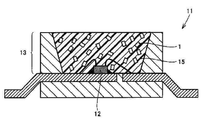
도 1은 본 발명의 바람직한 일례의 발광 장치(11)를 대략적으로 나타낸 단면도이다.
도 2는 본 발명의 다른 바람직한 일례의 발광 장치(21)를 대략적으로 나타낸 단면도이다.1 is a sectional view schematically showing a
2 is a sectional view schematically showing a
본 발명의 형광체는, 하기 일반식 (A)로 표시되는 β형 SiAlON (사이알론) 인 2가의 유로퓸 활성화 산질화물 녹색계 발광 형광체이다.The phosphor of the present invention is a divalent europium activated oxynitride green light emitting phosphor which is β-type SiAlON (sialon) represented by the following general formula (A).
일반식 (A) : EuaSibAlcOdNe General formula (A): Eu a Si b Al c O d N e
상기 일반식 (A) 중 a의 값은 0.005≤a≤0.4이고 b+c=12이고, d+e=16이다. 상기 일반식 (A) 중 a의 값이 0.005 미만이면 충분한 밝기를 얻을 수 없다는 문제가 있으며, a값이 0.4를 초과하면 농도 소광 등에 의해 밝기가 크게 저하하는 문제가 있다. 또한, 특성의 안정성, 모체의 균질성으로부터, 상기 일반식 (A)중의 a의 값은 0.01≤a≤0.2인 것이 바람직하다.The value of a in General Formula (A) is 0.005 ≦ a ≦ 0.4, b + c = 12, and d + e = 16. If the value of a in General Formula (A) is less than 0.005, there is a problem in that sufficient brightness cannot be obtained. If the value of a exceeds 0.4, there is a problem in that the brightness greatly decreases due to concentration quenching. Moreover, it is preferable that the value of a in the said general formula (A) is 0.01 <= a <= 0.2 from stability of a characteristic and homogeneity of a mother.
또한, 본 발명의 형광체의 평균 입도(d1)(공기 투과법)는 9~16μm이다. d1이 9μm 미만에서는, 결정 성장이 불충분한 주상 결정체(침상 결정체)나 소결체(응집체)가 많이 존재하고, 충분한 밝기가 얻어지지 않는다. 한편, d1이 16μm를 초과하면, 거칠고 큰 소결체(응집체)의 존재가 많아지고, 그의 크기에도 불구하고 충분한 밝기가 얻어지지 않는다. 특성의 안정성, 모체의 균질성으로부터 10μm≤d1≤13μm인 것이 바람직하다.In addition, the average particle size (d1) (air permeation method) of the fluorescent substance of this invention is 9-16 micrometers. When d1 is less than 9 micrometers, many columnar crystals (acicular crystals) and sintered compacts (aggregates) with insufficient crystal growth exist, and sufficient brightness is not obtained. On the other hand, when d1 exceeds 16 micrometers, the presence of a coarse and large sintered compact (aggregate) increases, and sufficient brightness is not obtained despite its size. It is preferable that it is 10 micrometer <d1 <= 13 micrometers from stability of a characteristic and homogeneity of a mother.
또한, 결정의 분산성을 나타내는 식 50% D/d1 (즉, 단일 입자의 존재 비율을 나타내는 지표)에서는, 1.4~2.2의 범위로 한정된다. 50% D/d1은 1.0이 이상적이지만, 50% D/d1가 1.4 미만인 경우, 분쇄가 과도하게 되는 경향이 있으며, 밝기의 저하를 무시할 수 없다. 반면, 50% D/d1가 2.2를 초과하면, 소결체(응집체)의 존재가 많아져 밝기가 현저히 저하한다. 특성의 안정성, 모체의 균질성으로부터, 1.6≤50% D/d1≤2.0인 것이 바람직하다.In addition, it is limited to the range of 1.4-2.2 in the formula 50% D / d1 (that is, the index which shows the existence ratio of a single particle) which shows the dispersibility of a crystal | crystallization. 50% D / d1 is ideally 1.0, but when 50% D / d1 is less than 1.4, the grinding tends to be excessive, and the decrease in brightness cannot be ignored. On the other hand, when 50% D / d1 exceeds 2.2, the presence of a sintered compact (aggregate) increases, and the brightness is significantly reduced. From the stability of the properties and the homogeneity of the mother, it is preferable that 1.6≤50% D / d1≤2.0.
따라서, 평균 입도(d1)(공기 투과법) 및 50% D/d1의 범위가 정해지면, 입도 분포에서의 메디안 직경(50% D)은 그에 따라 정해진다. 즉, 12.5~35μm의 범위를 갖게 된다.Therefore, if the average particle size d1 (air permeation method) and the range of 50% D / d1 are determined, the median diameter (50% D) in the particle size distribution is determined accordingly. That is, it has a range of 12.5-35 micrometers.
상술한, 평균 입도 (d1)(공기 투과법) 및 50% D/d1의 범위를 갖는 β형 SiAlON(사이알론)인 2가의 유로퓸 활성화 산질화물을 녹색계 발광 형광체에 있어서는, 체색(體色)이 우수하고, 600nm에서의 흡수율은 8.0% 이하의 값을 갖는다. 8.0%를 초과하면, 장파장 성분(특히, 적색계 영역)의 흡수를 무시할 수 없고, 백색의 밝기가 현저히 저하한다. 특성의 안정성, 모체의 균질성의 관점에서, 600nm에서의 흡수율은 7.0% 이하인 것이 바람직하다.In the green light emitting phosphor, the divalent europium activated oxynitride, which is a β-type SiAlON (sialon) having an average particle size (d1) (air permeation method) and a range of 50% D / d1, is used in a green light emitting phosphor. This is excellent, and the absorption at 600 nm has a value of 8.0% or less. When it exceeds 8.0%, absorption of the long wavelength component (particularly, the red region) cannot be ignored, and the brightness of white decreases significantly. From the viewpoint of stability of properties and homogeneity of the mother, the absorption at 600 nm is preferably 7.0% or less.
상기 식으로 표시되는 β형 SiAlON(사이알론)인 2가의 유로퓸 활성화 산질화물 녹색계 발광 형광체로서는, 구체적으로, Eu0.05Si11.50Al0.50O0.30N15.70, Eu0.10Si11.00Al1.00O0.40N15.60, Eu0.30Si9.80Al2.20O1.00N15.00, Eu0.15Si10.00Al2.00O0.50N15.50,Specific examples of the divalent europium activated oxynitride green luminescent phosphor of β-type SiAlON (sialon) represented by the above formula include Eu 0.05 Si 11.50 Al 0.50 O 0.30 N 15.70 , Eu 0.10 Si 11.00 Al 1.00 O 0.40 N 15.60 , Eu 0.30 Si 9.80 Al 2.20 O 1.00 N 15.00 , Eu 0.15 Si 10.00 Al 2.00 O 0.50 N 15.50 ,
Eu0.01Si11.60Al0.40O0.20N15.80, Eu0.005Si11.70Al0.30O0.15N15.85, Eu0.25Si11.65Al0.35O0.30N15.70, Eu0.40Si11.35Al0.65O0.35N15.65, Eu0.05Si11.55Al0.45O0.35N15.65 등을 열거할 수 있으나, 물론 이들에 한정되는 것은 아니다.Eu 0.01 Si 11.60 Al 0.40 O 0.20 N 15.80 , Eu 0.005 Si 11.70 Al 0.30 O 0.15 N 15.85 , Eu 0.25 Si 11.65 Al 0.35 O 0.30 N 15.70 , Eu 0.40 Si 11.35 Al 0.65 O 0.35 N 15.65 , Eu 0.05 Si 11.55 Al 0.45 O 0.35 N 15.65 and the like can be enumerated, of course, but is not limited to these.
또한, 평균 입도(d1)(공기 투과법)는 리-너스(Lea-Nurse)법, 블레인(Blaine)법 등에 의해 측정된 값을 말하며, 예컨대, 공기투과식 분체비표면적 측정 장치 (츠츠이 이화학 기계(주) 제품) 등을 사용함으로써 측정할 수 있다.In addition, the mean particle size d1 (air permeation method) refers to a value measured by the Lea-Nurse method, the Blaine method, or the like, and is, for example, an air permeable powder specific surface area measuring apparatus (Tsutsui Chemical Co., Ltd.). It can measure by using a machine, etc. product.
또한, 상기 메디안 직경(50% D)은, 입도 분포 측정 장치(LA-920, 호리바 제작소 제품)을 사용하여 측정된 값을 말한다. 또한, 입도 분포 측정 시에는, 전해질(소듐 헥사메타포스페이트)을 사용했지만, 초음파에 의한 예비 분산은 행하지 않았다.In addition, the said median diameter (50% D) says the value measured using the particle size distribution measuring apparatus (LA-920, Horiba Corporation make). In the particle size distribution measurement, an electrolyte (sodium hexametaphosphate) was used, but preliminary dispersion by ultrasonic waves was not performed.
또한, 600nm의 흡수율은, 예를 들어 분광 스펙트럼 측정 장치 MCPD7000 (오오츠카 전자(주) 제품)를 사용하여 측정할 수 있다.In addition, the absorbance of 600 nm can be measured using the spectral spectrum measuring apparatus MCPD7000 (made by Otsuka Electronics Co., Ltd.), for example.
본 발명의 형광체는, 종래 공지의 적절한 방법으로 제작할 수 있다. 단, 균일하게 결정 성장시키기 위해서는, 예를 들어 Al 농도(c)를 0.3 이상으로 하거나, 산소 농도를 정밀하게 제어하거나, 소성 용기 중의 원재료의 밀도 및 부피를 정밀하게 제어하거나, 합성시의 온도 프로파일을 최적화하는 방법을 들 수 있지만, 이들에 한정되는 것은 아니다.The phosphor of the present invention can be produced by a conventionally known appropriate method. However, for uniform crystal growth, for example, the Al concentration (c) is 0.3 or more, the oxygen concentration is precisely controlled, the density and volume of the raw materials in the firing vessel are precisely controlled, or the temperature profile at the time of synthesis Although the method of optimizing it is mentioned, it is not limited to these.
도 1은 본 발명의 바람직한 일례의 발광 장치(11)를 대략적으로 나타내는 단면도이다. 도 1에 나타낸 예의 본 발명의 발광 장치(11)에 사용되는 발광 소자(12)에는, 효율의 관점에서, 질화 갈륨(GaN)계 반도체가 사용된다. 또한, 본 발명의 발광 장치(11)에 있어서의 발광 소자(12)로서는, 피크 파장이 430 ~ 480nm 범위의 1차광을 발하는 것이 사용된다.1 is a sectional view schematically showing a
본 발명의 발광 장치(11)에 있어서, 파장 변환부(13)는, 상술한 본 발명의 형광체를 함유하고, 발광 소자(12)로부터 발해지는 1차광의 일부를 흡수하여, 1차광의 파장 이상의 길이의 파장을 갖는 2차광을 발할 수 있는 것이라면, 그 매질(15)은 특별히 제한되지 않는다. 매질(15)로서는, 예컨대 에폭시 수지, 실리콘 수지, 요소 수지 등의 투명 수지를 사용할 수 있으나 이들에 한정되는 것은 아니다. 구체적으로 말하면, 열경화형 실리콘 수지 봉지재 등이 매질(15)로서 적합하게 사용된다. 또한, 파장 변환부(13)는 본 발명의 효과를 저해하지 않는 범위에서, 적절한 SiO2, TiO2, ZrO2, Al2O3, Y2O3 등의 첨가제를 함유하고 있어도 물론 좋다.In the
도 2는 본 발명의 다른 바람직한 일례의 발광 장치(21)를 대략적으로 나타내는 단면도이다. 도 2에 나타낸 예와 같이, 본 발명의 발광 장치(21)의 파장 변환부(13)에는, 상술한 본 발명의 형광체(1) 이외의 형광체(14)가 포함되어 있어도 물론 좋다. 본 발명의 형광체(1) 이외에 파장 변환부(13)에 포함될 수 있는 다른 형광체(14)로서는 특별히 제한되는 것은 아니지만, 본 발명의 형광체(1)는 녹색계 발광 형광체로 구성되어 있기 때문에, 혼색에 의해 백색광을 나타내는 발광 장치를 실현할 수 있는 관점에서, 다음 일반식 (B)로 표시되는 2가의 유로퓸 활성화 질화물 적색계 발광 형광체가 적합하다.2 is a sectional view schematically showing a
일반식 (B) : (MI1-xEux) MIISiN3 General formula (B): (MI 1-x Eu x ) MIISiN 3
상기 일반식 (B) 중 MI는 Mg, Ca, Sr 및 Ba로부터 선택되는 적어도 1종의 알칼리 토류 금속 원소를 나타낸다. 또한 상기 일반식 (B) 중, MII는 Al, Ga, In, Sc, Y, La, Gd 및 Lu로부터 선택되는 적어도 1종의 3가의 금속 원소를 나타낸다. 그 중에서도, 더욱 높은 효율로 적색광을 발광할 수 있는 것으로부터, MII는 Al, Ga 및 In으로부터 선택되는 적어도 1종의 원소인 것이 바람직하다. 또한, 상기 일반식 (B) 중, x의 값은 0.001≤x≤0.10이고, 0.005≤x≤0.05인 것이 바람직하다. x의 값이 0.001 미만이면 충분한 밝기가 얻어지지 않는 경향이 있고, x의 값이 0.10을 초과하면, 농도 소광 등으로 밝기가 크게 저하하는 경향이 있기 때문이다.MI in the general formula (B) represents at least one alkaline earth metal element selected from Mg, Ca, Sr and Ba. In the formula (B), MII represents at least one trivalent metal element selected from Al, Ga, In, Sc, Y, La, Gd and Lu. Among them, MII is preferably at least one element selected from Al, Ga, and In because it can emit red light with higher efficiency. In the above general formula (B), the value of x is preferably 0.001 ≦ x ≦ 0.10, and preferably 0.005 ≦ x ≦ 0.05. It is because there exists a tendency for sufficient brightness not to be acquired that the value of x is less than 0.001, and there exists a tendency for brightness to fall largely by concentration quenching etc. when the value of x exceeds 0.10.
이러한 2가의 유로퓸 활성화 질화물 적색계 발광 형광체로서는, 구체적으로, (Ca0.99Eu0.01) AlSiN3, (Ca0.97Mg0.02Eu0.01) (Al0.99Ga0.01) SiN3, (Ca0.98Eu0.02) AlSiN3, (Ca0.58Sr0.40Eu0.02) (Al0.98In0.02) SiN3, (Ca0.999Eu0.001) AlSiN3, (Ca0.895Sr0.100Eu0.005) AlSiN3, (Ca0.79Sr0.20Eu0.01) AlSiN3, (Ca0.98Eu0.02) (Al0.95Ga0.05) SiN3, (Ca0.20Sr0.79Eu0.01) AlSiN3, (Ca0.58Sr0.40Eu0.02) AlSiN3 등을 들 수 있으나, 물론 이들에 한정되는 것은 아니다.Specific examples of such divalent europium activated nitride red light-emitting phosphors include (Ca 0.99 Eu 0.01 ) AlSiN 3 , (Ca 0.97 Mg 0.02 Eu 0.01 ) (Al 0.99 Ga 0.01 ) SiN 3 , (Ca 0.98 Eu 0.02 ) AlSiN 3 , ( Ca 0.58 Sr 0.40 Eu 0.02 ) (Al 0.98 In 0.02 ) SiN 3 , (Ca 0.999 Eu 0.001 ) AlSiN 3 , (Ca 0.895 Sr 0.100 Eu 0.005 ) AlSiN 3 , (Ca 0.79 Sr 0.20 Eu 0.01 ) AlSiN 3 , (Ca 0.98 Eu 0.02 ) (Al 0.95 Ga 0.05 ) SiN 3 , (Ca 0.20 Sr 0.79 Eu 0.01 ) AlSiN 3 , (Ca 0.58 Sr 0.40 Eu 0.02 ) AlSiN 3 , and the like, but are not limited thereto.
또한, 상술한 2가의 유로퓸 활성화 질화물 적색계 발광 형광체를 사용하는 경우, 파장 변환부(13)에 있어서의 본 발명의 형광체와의 혼합 비율로서는, 특별히 제한되는 것은 아니지만, 본 발명의 형광체에 대해, 중량비로 1~35%의 범위 내로 하는 것이 바람직하고, 5~25% 범위 내로 하는 것이 더욱 바람직하다.In addition, when using the bivalent europium activated nitride red light-emitting fluorescent substance mentioned above, as a mixing ratio with the fluorescent substance of this invention in the
본 발명의 발광 장치(11)에 있어서의 파장 변환부(13)는, 본 발명의 효과를 저해하지 않는 범위에서, 상술한 2가의 유로퓸 활성화 질화물 적색계 발광 형광체 이외의, 본 발명의 형광체 이외의 형광체를 포함하고 있어도 물론 좋다. 또한, 이러한 본 발명의 형광체, 상술한 2가의 유로퓸 활성화 질화물 적색계 발광 형광체 이외의 형광체는, 본 발명의 형광체 및 상술한 2가의 유로퓸 활성화 질화물 적색계 발광 형광체에 더해, 파장 변환부(13)에 더 포함되어 있어도 좋다.The
본 발명의 발광 장치(21)에 사용되는 발광 소자(12)에는, 효율의 관점에서, 질화 갈륨(GaN)계 반도체가 사용된다. 또한, 본 발명의 발광 장치(21)에 있어서의 발광 소자(12)로서는, 피크 파장이 430 ~ 480nm 범위의 1차광을 발하는 것이 사용된다. 피크 파장이 430nm 미만의 발광 소자를 사용한 경우에는, 청색 성분의 기여가 적어져, 연색성이 나빠지고 실용적이 아니기 때문이며, 피크 파장이 480nm를 초과하는 발광 소자를 사용한 경우에는, 백색에서의 밝기가 저하하고, 실용적이 아니기 때문이다. 효율성의 관점에서, 본 발명의 발광 장치(21)에 있어서의 발광 소자(12)는, 440 ~ 470nm 범위의 1차광을 발하는 것이 바람직하다.As the
본 발명의 발광 장치(11,21)는, 종래 공지의 적절한 수법으로 제조할 수 있으며, 그 제조 방법은 특별히 제한되는 것은 아니다. 예를 들어, 매질(15)로서 열경화형의 실리콘 수지 봉지재를 사용하고, 이에 본 발명의 형광체(1)(필요에 따라 본 발명의 형광체 이외의 형광체 14)를 혼련하고, 발광 소자(12)를 봉지하고 성형하여, 제조하는 경우가 예시된다.The
본 발명은 또한, 상술한 본 발명의 발광 장치를 점광원으로서 복수 포함한 백라이트 광원 장치를 제공한다. 본 발명은 또한, 액정 패널과, 액정 패널의 배면에 배치된 상술한 본 발명의 백라이트 광원 장치를 갖는 액정 표시 장치를 제공한다. 본 발명의 액정 표시 장치는, 예를 들어, 발광 장치를 복수 준비하고, 케이싱에 매트릭스 형태로 탑재한 직하형 백라이트 광원 장치를 배치하고, 백라이트 광원 장치 상에 광학 시트, 액정 패널을 배치하여 구성된다. 또한, 직하형 백라이트 광원 장치 대신, 상술한 본 발명의 발광 장치를 복수 준비하고, 도광판 측면에 배치하고, 도광판 이면에는 반사판이 설치되고, 도광판 표면으로부터 빛을 취출하는 구성의 에지 라이트 방식의 백라이트 광원 장치로 치환하도록 해도 좋다.The present invention also provides a backlight light source device including a plurality of the above-described light emitting devices of the present invention as a point light source. This invention also provides the liquid crystal display device which has a liquid crystal panel and the backlight light source device of the above-mentioned this invention arrange | positioned at the back surface of a liquid crystal panel. The liquid crystal display device of the present invention is configured by, for example, preparing a plurality of light emitting devices, arranging a direct backlight light source device mounted in a casing in a casing, and arranging an optical sheet and a liquid crystal panel on the backlight light source device. . In addition, instead of the direct backlight type light source device, a plurality of light emitting devices of the present invention described above are prepared, disposed on the side of the light guide plate, and a reflecting plate is provided on the rear surface of the light guide plate, and the edge light type backlight light source is configured to extract light from the light guide plate surface. It may be replaced by a device.
이하, 실시예 및 비교예를 들어 본 발명을 보다 상세하게 설명하지만, 본 발명은 이들에 한정되는 것은 아니다.Hereinafter, although an Example and a comparative example are given and this invention is demonstrated in detail, this invention is not limited to these.
<실시예 1, 비교예 1><Example 1, Comparative Example 1>
발광 소자로서 450nm에 피크 파장을 갖는 질화 갈륨(GaN)계 반도체를 사용했다. 파장 변환부에는, Eu0.05Si11.55Al0.45O0.35N15.65(β형 SiAlON)의 조성을 갖는 녹색계 발광 형광체로서, 평균 입도(d1)가 11.3μm, 메디안 직경(50% D)이 18.6μm, 50% D/d1=1.65, 600 nm에 있어서의 흡수율이 5.9%인 특성 값을 갖는 것을 사용했다. 또한, 이 형광체는 주로, Al 농도(c)를 0.50으로 제어함으로써 조제된 것이다. 이 형광체를, 소정의 비율로 매질로서의 열경화형의 실리콘 수지 봉지 재에 분산시켜 분산하고, 발광 소자를 봉지하여, 파장 변환부를 형성하고, 실시예 1의 발광 장치를 제작했다. 이와 같이 하여 제작한 실시예 1의 발광 장치에 대해, 초기 및 5000 시간 후의 밝기를 측정했다. 또한 밝기는 순방향 전류(IF) 30mA에서 점등하고, 발광 장치로부터의 광 출력(광 전류)을 측정했다.As a light emitting element, a gallium nitride (GaN) -based semiconductor having a peak wavelength at 450 nm was used. The wavelength conversion portion is a green light-emitting phosphor having a composition of Eu 0.05 Si 11.55 Al 0.45 O 0.35 N 15.65 (β type SiAlON), with an average particle size (d1) of 11.3 μm and a median diameter (50% D) of 18.6 μm, 50. The thing which has the characteristic value whose absorption in% D / d1 = 1.65 and 600 nm is 5.9% was used. In addition, this fluorescent substance is mainly prepared by controlling Al concentration (c) to 0.50. This phosphor was dispersed and dispersed in a thermosetting silicone resin encapsulant as a medium at a predetermined ratio, the light emitting element was encapsulated, a wavelength conversion portion was formed, and the light emitting device of Example 1 was produced. The brightness | luminance after the initial stage and 5000 hours was measured about the light emitting device of Example 1 produced in this way. In addition, the brightness was turned on at 30 mA of forward current IF, and the light output (light current) from the light emitting device was measured.
한편, Eu0.05Si11.93Al0.07O0.10N15.90(β형 SiAlON)의 조성을 갖는 녹색계 발광 형광체로서, 평균 입도(d1)가 6.5μm, 메디안 직경(50% D)이 19.5μm, 50% D/d1 = 3.00, 600 nm에 있어서의 흡수율이 12.0%인 특성 값을 갖는 것을 사용한 것 이외는 상기와 마찬가지로 하여, 비교예 1의 발광 장치를 제작하고, 동일하게 특성을 평가했다.On the other hand, a green light emitting phosphor having a composition of Eu 0.05 Si 11.93 Al 0.07 O 0.10 N 15.90 (β-type SiAlON), having an average particle size (d1) of 6.5 μm and a median diameter (50% D) of 19.5 μm and 50% D / The light emitting device of Comparative Example 1 was produced in the same manner as above except that the absorbance at d1 = 3.00 and 600 nm was 12.0%, and the characteristics were evaluated in the same manner.
실시예 1, 비교예 1의 결과를 표 1에 나타낸다. 표 1로부터, 실시예 1의 발광 장치는 비교예 1의 발광 장치와 비교하여 상당히 밝고 또한 밝기의 변동이 적다는 것을 알 수 있다.Table 1 shows the results of Example 1 and Comparative Example 1. From Table 1, it can be seen that the light emitting device of Example 1 is considerably brighter and there is less variation in brightness as compared with the light emitting device of Comparative Example 1.
<실시예 2, 3, 비교예 2, 3><Examples 2 and 3, Comparative Examples 2 and 3>
표 2에 나타낸 바와 같은 각종 평균 입도(d1), 메디안 직경(50% D), 50% D/d1 값, 600nm에 있어서의 흡수율을 갖는 형광체를 사용한 것을 제외하고는 실시예 1과 동일하게 하여, 각각 실시예 2,3, 비교예 2,3의 발광 장치를 제작했다. 실시예 1과 동일하게 하여 측정한 특성(밝기)의 결과를 표 3에 나타낸다. 표 3으로부터, 실시예 2,3의 발광 장치는 비교예 2,3의 발광 장치에 비해 현저하게 밝고 또한 밝기의 변동이 적다는 것을 알 수 있다.In the same manner as in Example 1, except that phosphors having various average particle sizes (d1), median diameters (50% D), 50% D / d1 values, and absorption at 600 nm as shown in Table 2 were used. The light emitting devices of Examples 2 and 3 and Comparative Examples 2 and 3 were produced, respectively. Table 3 shows the results of the characteristics (brightness) measured in the same manner as in Example 1. From Table 3, it can be seen that the light emitting devices of Examples 2 and 3 are significantly brighter and have less variation in brightness than the light emitting devices of Comparative Examples 2 and 3.
(d1)(μm)Average particle size
(d1) (μm)
(μm)50% D
(μm)
흡수율(%)600 nm
Absorption rate (%)
<실시예 4, 비교예 4><Example 4, Comparative Example 4>
발광 소자로서, 460nm에 피크 파장을 갖는 질화 갈륨(GaN)계 반도체를 사용했다. 파장 변환부에는, Eu0.05Si11.55Al0.45O0.35N15.65(β형 SiAlON)의 조성을 갖는 녹색계 발광 형광체로서, 평균 입도(d1)가 11.3μm, 메디안 직경(50% D)이 18.6μm, 50% D/d1=1.65, 600nm에 있어서의 흡수율이 5.9%인 특성 값을 갖는 것으로, (Ca0.99Eu0.01) AlSiN3 (D50 값 : 12.8μm)의 조성을 갖는 2가의 유로퓸 활성화 질화물 적색계 발광 형광체를 사용했다. 이 형광체 및 적색계 발광 형광체를 소정의 비율로 매질로서의 열경화형의 실리콘 수지 봉지재에 분산시켜 분산하고, 발광 소자를 봉지하여 파장 변환부를 형성하고, 실시예 4의 발광 장치를 제작했다. 이렇게 제작한 실시예 4의 발광 장치에 대해, 초기 및 5000 시간 후의 밝기 및 색도를 측정하였다. 또한, 밝기는 순방향 전류(IF) 30mA에서 점등하고, 발광 장치로부터의 광 출력(광 전류)을 측정하고, 색도는 MCPD-2000(오츠카 전자 제품)를 이용해 측정했다.As a light emitting element, a gallium nitride (GaN) -based semiconductor having a peak wavelength at 460 nm was used. The wavelength conversion portion is a green light-emitting phosphor having a composition of Eu 0.05 Si 11.55 Al 0.45 O 0.35 N 15.65 (β type SiAlON), with an average particle size (d1) of 11.3 μm and a median diameter (50% D) of 18.6 μm, 50. A divalent europium-activated nitride red light-emitting phosphor having a composition of (Ca 0.99 Eu 0.01 ) AlSiN 3 (D50 value: 12.8 μm) having a characteristic value at a absorption rate of 5.9% at% D / d1 = 1.65 and 600 nm was used. did. The phosphor and the red light-emitting phosphor were dispersed and dispersed in a thermosetting silicone resin encapsulant as a medium at a predetermined ratio, and the light emitting element was encapsulated to form a wavelength conversion portion to manufacture the light emitting device of Example 4. About the light emitting device of Example 4 thus produced, brightness and chromaticity of the initial stage and after 5000 hours were measured. In addition, the brightness was lighted at 30 mA of forward current IF, the light output from the light emitting device (light current) was measured, and the chromaticity was measured using MCPD-2000 (Otsuka Electronics Co., Ltd.).
한편, Eu0.05Si11.93Al0.07O0.10N15.90(β형 SiAlON)의 조성을 갖는 녹색계 발광 형광체로서, 평균 입도 (d1)가 6.5μm, 메디안 직경 (50% D)이 19.5μm, 50% D/d1 = 3.00, 600 nm에 있어서의 흡수율이 12.0%인 특성 값을 갖는 것을 사용한 것은 실시예 4와 동일하게 하여, 비교예 4의 발광 장치를 제작했다.On the other hand, a green light emitting phosphor having a composition of Eu 0.05 Si 11.93 Al 0.07 O 0.10 N 15.90 (β-type SiAlON), having an average particle size (d1) of 6.5 μm and a median diameter (50% D) of 19.5 μm and 50% D / A light emitting device of Comparative Example 4 was produced in the same manner as in Example 4 that d1 = 3.00 and the one having a characteristic value having an absorptivity at 600 nm were 12.0%.
이들 실시예 4, 비교예 4의 발광 장치에 대해, 실시예 1과 동일하게 하여 특성(밝기 및 색도) 평가를 행했다. 결과를 표 4에 나타낸다. 표 4로부터, 실시예 4의 발광 장치는 비교예 4의 발광 장치와 비교하여, 현저히 밝고 또한 밝기 및 색도의 변동이 적은 것을 알 수 있다.The characteristics (brightness and chromaticity) of these light emitting devices of Example 4 and Comparative Example 4 were evaluated in the same manner as in Example 1. The results are shown in Table 4. From Table 4, it can be seen that the light emitting device of Example 4 is significantly brighter and has less variation in brightness and chromaticity than in the light emitting device of Comparative Example 4.
(상대값)brightness
(Relative value)
(유지율)brightness
(Retention rate)
<실시예 5~9, 비교예 5~9><Examples 5-9, Comparative Examples 5-9>
표 5에 나타낸 바와 같은 각종 평균 입도 (d1), 메디안 직경 (50% D), 50% D/d1 값, 600nm에 있어서의 흡수율을 갖는 β형 SiAlON 형광체를 사용한 것을 제외하고는 실시예 4와 동일하게 하여, 각각 실시예 5~9, 비교예 5~9의 발광 장치를 제작했다. 실시예 4와 동일하게 하여 측정한 특성(밝기 및 색도)의 평가 결과를 표 6에 나타낸다. 표 6으로부터, 실시예 5~9의 발광 장치는 비교예 5~9의 발광 장치에 비해 현저히 밝고 또한 밝기 및 색도의 변동이 적은 것을 알 수 있다.Same as Example 4 except for using a β-type SiAlON phosphor having various average particle sizes (d1), median diameter (50% D), 50% D / d1 value, and absorption at 600 nm as shown in Table 5. Thus, the light emitting devices of Examples 5 to 9 and Comparative Examples 5 to 9 were produced, respectively. Table 6 shows evaluation results of the characteristics (brightness and chromaticity) measured in the same manner as in Example 4. From Table 6, it can be seen that the light emitting devices of Examples 5 to 9 are significantly brighter and have less variation in brightness and chromaticity than the light emitting devices of Comparative Examples 5 to 9.


본 발명의 발광 장치는 본 발명의 형광체를 포함하는 파장 변환부를 구비한 것이다. 이러한 본 발명의 발광 장치는, 발광 소자로부터의 1차광을 효율적으로 흡수하고, 고효율로 우수한 색 재현성(NTSC비), 양호한 온도 및 수명 특성의 백색광을 얻을 수 있다.The light emitting device of the present invention includes a wavelength converting portion containing the phosphor of the present invention. Such a light emitting device of the present invention efficiently absorbs primary light from a light emitting element, and can obtain white light having excellent color reproducibility (NTSC ratio), good temperature, and lifetime characteristics with high efficiency.
이상의 실시예 1~9에 열거된 어느 것의 발광 장치를 복수 준비하고, 케이싱에 매트릭스 형태로 탑재한 직하형 백라이트 발광 장치를 구성하고, 백라이트 광원 장치 상에 광학 시트, 액정 패널을 배치하여 구성된 액정 표시 장치(TV)를 구성하면 색 재현성이 뛰어난 액정 표시 장치가 얻어진다. 또한, 직하형 백라이트 광원 장치 대신, 실시예 1~9에 열거된 어느 것의 발광 장치를 복수 준비하고, 도광판 측면에 배치하고, 도광판 이면에는 반사판을 설치하고, 도광판 표면으로부터 빛을 취출하는 구성의 에지 라이트 방식의 백라이트 광원 장치로 치환해도 상관없다.A liquid crystal display comprising a plurality of light emitting devices listed in Examples 1 to 9 prepared above, a direct type backlight light emitting device mounted on a casing in a matrix form, and an optical sheet and a liquid crystal panel disposed on the backlight light source device. When the apparatus TV is comprised, the liquid crystal display device excellent in color reproducibility is obtained. In addition, instead of the direct type backlight light source device, a plurality of light emitting devices listed in Examples 1 to 9 are prepared, disposed on the light guide plate side surface, a reflecting plate is provided on the back surface of the light guide plate, and the light is extracted from the light guide plate surface. It may replace with the backlight type light source device.
금회 개시된 실시 형태 및 실시예는 모든 점에서 예시적이며 제한적인 것이 아닌 것으로 고려되어야 한다. 본 발명의 범위는 상기한 설명이 아니라 청구 범위에 의해 정해지고, 청구 범위와 균등의 의미 및 범위 내에서의 모든 변경이 포함되는 것이다.The disclosed embodiments and examples are to be considered in all respects as illustrative and not restrictive. The scope of the present invention is defined by the claims rather than the foregoing description, and includes the meanings of the claims and equivalents and all modifications within the scope.
1 : 형광체
11,21 : 발광 장치
12 : 발광 소자
13 : 파장 변환부
14 : 본 발명의 형광체 이외의 형광체
15 : 매질1: phosphor
11,21: light emitting device
12: light emitting element
13 wavelength conversion unit
14: Phosphors other than the phosphor of the present invention
15: medium
Claims (12)
(일반식 (A) 중 0.005≤a≤0.4, b+c=12, d+e=16을 만족하는 수이다.)로 실질적으로 표시되고, 평균 입도(d1)(공기 투과법)가 9~16μm이고, 입도 분포에서의 메디안 직경 (50% D)이 12.5~35μm이고, 50% D/d1=1.4~2.2이고, 또한 600nm에 있어서의 흡수율이 8.0% 이하인 β형 SiAlON인, 2가의 유로퓸 활성화 산질화물 녹색계 발광 형광체.General formula (A): Eu a Si b Al c O d N e
(It is the number which satisfy | fills 0.005 <= a <= 0.4, b + c = 12, d + e = 16 in General formula (A).) It is shown substantially, and the average particle size d1 (air permeation method) is 9-. Divalent europium activation with 16 μm, β-type SiAlON having a median diameter (50% D) in the particle size distribution of 12.5 to 35 μm, 50% D / d1 = 1.4 to 2.2, and an absorption at 600 nm of 8.0% or less. Oxynitride green-based phosphor.
일반식 (A) : EuaSibAlcOdNe
(일반식 (A) 중 0.005≤a≤0.4, b+c=12, d+e=16을 만족하는 수이다.)로 실질적으로 표시되고, 평균 입도(d1) (공기 투과법)가 9~16μm이고, 입도 분포에서의 메디안 직경(50% D)이 12.5~35μm이고, 50% D/d1=1.4~2.2이고, 또한 600nm에 있어서의 흡수율이 8.0% 이하인 β형 SiAlON인, 2가의 유로퓸 활성화 산질화물 녹색계 발광 형광체를 포함하는, 발광 장치.A light emitting device comprising a light emitting element which is a gallium nitride-based semiconductor that emits primary light having a peak wavelength of 430 nm to 480 nm, and a wavelength converter that absorbs a part of the primary light and emits secondary light having a wavelength longer than that of the primary light. The wavelength converter,
General formula (A): Eu a Si b Al c O d N e
(It is a number which satisfy | fills 0.005 <= a <= 0.4, b + c = 12, d + e = 16 in General formula (A).) It is shown substantially and average particle size (d1) (air permeation method) is 9-. Divalent europium activation with 16 μm, β-type SiAlON with median diameter (50% D) in the particle size distribution of 12.5-35 μm, 50% D / d1 = 1.4-2.2, and absorption at 600 nm of 8.0% or less A light emitting device comprising an oxynitride green light emitting phosphor.
일반식 (B) : (MI1-xEux) MIISiN3
(일반식 (B) 중 MI는 Mg, Ca, Sr 및 Ba로부터 선택되는 적어도 1종의 알칼리 토류 금속 원소를 나타내며, MII는 Al, Ga, In, Sc, Y, La, Gd 및 Lu로부터 선택되는 적어도 1종의 3가의 금속 원소를 나타내고, 0.001≤x≤0.10을 만족하는 수이다.)로 실질적으로 표시되는 2가의 유로퓸 활성화 질화물 적색계 발광 형광체를 파장 변환부에 포함하는, 발광 장치.The method of claim 5,
General formula (B): (MI 1-x Eu x ) MIISiN 3
(In formula (B), MI represents at least one alkaline earth metal element selected from Mg, Ca, Sr and Ba, and MII is selected from Al, Ga, In, Sc, Y, La, Gd and Lu). And a divalent europium-activated nitride red light-emitting phosphor represented by at least one trivalent metal element and substantially expressed by 0.001 ≦ x ≦ 0.10.
액정 패널의 배면에 배치된 제11항에 기재된 백라이트 광원 장치를 구비하는, 액정 표시 장치.With a liquid crystal panel,
The liquid crystal display device provided with the backlight light source device of Claim 11 arrange | positioned at the back surface of a liquid crystal panel.
Applications Claiming Priority (3)
| Application Number | Priority Date | Filing Date | Title |
|---|---|---|---|
| JP2010003058 | 2010-01-08 | ||
| JPJP-P-2010-003058 | 2010-01-08 | ||
| PCT/JP2010/072684 WO2011083671A1 (en) | 2010-01-08 | 2010-12-16 | Phosphor, light-emitting device, and liquid crystal display device using same |
Publications (2)
| Publication Number | Publication Date |
|---|---|
| KR20120048020A true KR20120048020A (en) | 2012-05-14 |
| KR101378813B1 KR101378813B1 (en) | 2014-03-27 |
Family
ID=44305408
Family Applications (1)
| Application Number | Title | Priority Date | Filing Date |
|---|---|---|---|
| KR1020127006888A KR101378813B1 (en) | 2010-01-08 | 2010-12-16 | Phosphor, Light Emitting Apparatus, and Liquid Crystal Display Apparatus Using the Same |
Country Status (8)
| Country | Link |
|---|---|
| US (2) | US8709283B2 (en) |
| EP (1) | EP2468836A4 (en) |
| JP (2) | JP5589002B2 (en) |
| KR (1) | KR101378813B1 (en) |
| CN (1) | CN102656248B (en) |
| BR (1) | BR112012016731A2 (en) |
| TW (1) | TWI468495B (en) |
| WO (1) | WO2011083671A1 (en) |
Cited By (3)
| Publication number | Priority date | Publication date | Assignee | Title |
|---|---|---|---|---|
| JP2013163738A (en) * | 2012-02-09 | 2013-08-22 | Denki Kagaku Kogyo Kk | Phosphor and light-emitting device |
| JP2013163721A (en) * | 2012-02-09 | 2013-08-22 | Denki Kagaku Kogyo Kk | Phosphor and light-emitting device |
| JP2013163720A (en) * | 2012-02-09 | 2013-08-22 | Denki Kagaku Kogyo Kk | Phosphor and light-emitting device |
Families Citing this family (8)
| Publication number | Priority date | Publication date | Assignee | Title |
|---|---|---|---|---|
| JP5367218B2 (en) | 2006-11-24 | 2013-12-11 | シャープ株式会社 | Method for manufacturing phosphor and method for manufacturing light emitting device |
| JPWO2009110285A1 (en) | 2008-03-03 | 2011-07-14 | シャープ株式会社 | Light emitting device |
| EP2468836A4 (en) * | 2010-01-08 | 2014-07-30 | Sharp Kk | Phosphor, light-emitting device, and liquid crystal display device using same |
| EP2767573B1 (en) * | 2012-12-14 | 2016-09-28 | Denka Company Limited | Phosphor, method for producing same, and light emitting device |
| KR102353443B1 (en) | 2014-12-22 | 2022-01-21 | 삼성전자주식회사 | Oxynitride-based phosphor and white light emitting device including the same |
| WO2017122800A1 (en) * | 2016-01-15 | 2017-07-20 | デンカ株式会社 | Phosphor and light emitting device |
| EP3669115B1 (en) | 2017-08-18 | 2023-10-04 | Thorlabs, Inc. | Broadband light source based on crystalline phosphor |
| KR20220002390A (en) | 2019-04-23 | 2022-01-06 | 덴카 주식회사 | Phosphor powder and light emitting device |
Family Cites Families (24)
| Publication number | Priority date | Publication date | Assignee | Title |
|---|---|---|---|---|
| US6608332B2 (en) | 1996-07-29 | 2003-08-19 | Nichia Kagaku Kogyo Kabushiki Kaisha | Light emitting device and display |
| TW383508B (en) | 1996-07-29 | 2000-03-01 | Nichia Kagaku Kogyo Kk | Light emitting device and display |
| JP3609709B2 (en) | 2000-09-29 | 2005-01-12 | 株式会社シチズン電子 | Light emitting diode |
| WO2003107441A2 (en) | 2002-06-13 | 2003-12-24 | Cree, Inc. | Saturated phosphor solid emitter |
| KR100609830B1 (en) | 2003-04-25 | 2006-08-09 | 럭스피아 주식회사 | White Semiconductor Light Emitted Device using Green-emitting and Red emitting Phosphor |
| JP3921545B2 (en) | 2004-03-12 | 2007-05-30 | 独立行政法人物質・材料研究機構 | Phosphor and production method thereof |
| JP4517783B2 (en) | 2004-08-31 | 2010-08-04 | 日亜化学工業株式会社 | Rare earth boroaluminate phosphor and light emitting device using the same |
| WO2006033239A1 (en) | 2004-09-22 | 2006-03-30 | Kabushiki Kaisha Toshiba | Light emitting device, and back light and liquid crystal display employing it |
| JP4934792B2 (en) * | 2005-08-04 | 2012-05-16 | Dowaエレクトロニクス株式会社 | Phosphor, method for producing the same, and light emitting device using the phosphor |
| US8147715B2 (en) * | 2005-12-08 | 2012-04-03 | National Institute For Materials Science | Phosphor, process for producing the same, and luminescent device |
| CN101379163B (en) | 2006-02-02 | 2013-01-02 | 三菱化学株式会社 | Complex oxynitride phosphor, light-emitting device using same, image display, illuminating device, phosphor-containing composition and complex oxynitride |
| KR101204573B1 (en) * | 2006-05-10 | 2012-11-26 | 덴끼 가가꾸 고교 가부시키가이샤 | Sialon phosphor, process for producing the same, and illuminator and luminescent element employing the same |
| JP2007308593A (en) * | 2006-05-18 | 2007-11-29 | Denki Kagaku Kogyo Kk | Process for production of sialon fluorescent material, sialon fluorescent material and fluorescent light assembly |
| EP2036966B1 (en) * | 2006-07-05 | 2017-10-25 | Ube Industries, Ltd. | Sialon-base oxynitride phosphors and process for production thereof |
| JP2008120938A (en) * | 2006-11-14 | 2008-05-29 | Sharp Corp | Phosphor, its manufacturing method, semiconductor light emitting device and image display device |
| TWI357927B (en) | 2006-11-20 | 2012-02-11 | Denki Kagaku Kogyo Kk | Fluorescent substance and manufacturing method the |
| JP5367218B2 (en) | 2006-11-24 | 2013-12-11 | シャープ株式会社 | Method for manufacturing phosphor and method for manufacturing light emitting device |
| CN101688115B (en) | 2007-07-09 | 2013-03-27 | 夏普株式会社 | Group of phosphor particles, and light-emitting device using the same |
| JP2009019163A (en) * | 2007-07-13 | 2009-01-29 | Sharp Corp | Phosphor particle aggregate for light emitting device, light emitting device, and backlight device for liquid crystal display |
| JP2009092253A (en) | 2007-10-04 | 2009-04-30 | Masaji Furukawa | Double chimney combustion appliance |
| JP5316414B2 (en) * | 2007-10-10 | 2013-10-16 | 宇部興産株式会社 | Method for producing β-sialon phosphor particles |
| JP2009167338A (en) * | 2008-01-18 | 2009-07-30 | Sharp Corp | Wavelength conversion member, light emitting device having it, and phosphor |
| EP2468836A4 (en) * | 2010-01-08 | 2014-07-30 | Sharp Kk | Phosphor, light-emitting device, and liquid crystal display device using same |
| JP4740379B1 (en) | 2010-02-25 | 2011-08-03 | 電気化学工業株式会社 | β-type sialon phosphor, its use and method for producing β-type sialon phosphor |
-
2010
- 2010-12-16 EP EP10842184.3A patent/EP2468836A4/en not_active Ceased
- 2010-12-16 US US13/500,803 patent/US8709283B2/en active Active
- 2010-12-16 BR BR112012016731A patent/BR112012016731A2/en not_active Application Discontinuation
- 2010-12-16 CN CN201080054430.1A patent/CN102656248B/en active Active
- 2010-12-16 KR KR1020127006888A patent/KR101378813B1/en active IP Right Grant
- 2010-12-16 WO PCT/JP2010/072684 patent/WO2011083671A1/en active Application Filing
- 2010-12-16 JP JP2011548943A patent/JP5589002B2/en active Active
- 2010-12-27 TW TW99146167A patent/TWI468495B/en active
-
2014
- 2014-04-09 US US14/248,664 patent/US9496463B2/en active Active
- 2014-07-22 JP JP2014149016A patent/JP2014209660A/en active Pending
Cited By (3)
| Publication number | Priority date | Publication date | Assignee | Title |
|---|---|---|---|---|
| JP2013163738A (en) * | 2012-02-09 | 2013-08-22 | Denki Kagaku Kogyo Kk | Phosphor and light-emitting device |
| JP2013163721A (en) * | 2012-02-09 | 2013-08-22 | Denki Kagaku Kogyo Kk | Phosphor and light-emitting device |
| JP2013163720A (en) * | 2012-02-09 | 2013-08-22 | Denki Kagaku Kogyo Kk | Phosphor and light-emitting device |
Also Published As
| Publication number | Publication date |
|---|---|
| CN102656248A (en) | 2012-09-05 |
| CN102656248B (en) | 2014-07-16 |
| KR101378813B1 (en) | 2014-03-27 |
| JPWO2011083671A1 (en) | 2013-05-13 |
| US20140218658A1 (en) | 2014-08-07 |
| EP2468836A4 (en) | 2014-07-30 |
| TWI468495B (en) | 2015-01-11 |
| US20120194762A1 (en) | 2012-08-02 |
| US9496463B2 (en) | 2016-11-15 |
| TW201134922A (en) | 2011-10-16 |
| US8709283B2 (en) | 2014-04-29 |
| EP2468836A1 (en) | 2012-06-27 |
| JP5589002B2 (en) | 2014-09-10 |
| BR112012016731A2 (en) | 2018-05-15 |
| WO2011083671A1 (en) | 2011-07-14 |
| JP2014209660A (en) | 2014-11-06 |
Similar Documents
| Publication | Publication Date | Title |
|---|---|---|
| KR101378813B1 (en) | Phosphor, Light Emitting Apparatus, and Liquid Crystal Display Apparatus Using the Same | |
| US10259997B2 (en) | Phosphor, method of producing the same, and light emitting apparatus | |
| EP2175006B1 (en) | Group of phosphor particles, and light-emitting device using the same | |
| US20110279016A1 (en) | Carbonitride based phosphors and light emitting devices using the same | |
| JP5791034B2 (en) | Light emitting device | |
| US8801969B2 (en) | Carbonitride and carbidonitride phosphors and lighting devices using the same | |
| JPWO2011002087A1 (en) | Light emitting device | |
| KR101250838B1 (en) | Group of phosphor particles, light-emitting device using same, and liquid crystal television receiver | |
| JP2009076656A (en) | Light emitting device, image display device and liquid crystal display | |
| JP2010196049A (en) | Phosphor and method for producing the same, phosphor-containing composition, and light-emitting device, image display device and lighting device using the phosphor | |
| JP4948015B2 (en) | Aluminate blue phosphor and light emitting device using the same | |
| JP2015000953A (en) | Oxynitride-based fluorescent material and light-emitting device using the same | |
| JP2013227527A (en) | Phosphor and light emitting device using the same | |
| JP7022931B2 (en) | Fluorescent material and light emitting device | |
| JP2015196717A (en) | Phosphor, phosphor-containing compound, light-emitting device, image display device, and illuminating device | |
| JP2013122048A (en) | Oxynitride-based phosphor and light-emitting device using the same |
Legal Events
| Date | Code | Title | Description |
|---|---|---|---|
| A201 | Request for examination | ||
| E902 | Notification of reason for refusal | ||
| E701 | Decision to grant or registration of patent right | ||
| GRNT | Written decision to grant | ||
| FPAY | Annual fee payment |
Payment date: 20170315 Year of fee payment: 4 |
|
| FPAY | Annual fee payment |
Payment date: 20180308 Year of fee payment: 5 |