WO2011071017A1 - ジアザボロール化合物、およびそれを含有した電界効果トランジスタ - Google Patents
ジアザボロール化合物、およびそれを含有した電界効果トランジスタ Download PDFInfo
- Publication number
- WO2011071017A1 WO2011071017A1 PCT/JP2010/071828 JP2010071828W WO2011071017A1 WO 2011071017 A1 WO2011071017 A1 WO 2011071017A1 JP 2010071828 W JP2010071828 W JP 2010071828W WO 2011071017 A1 WO2011071017 A1 WO 2011071017A1
- Authority
- WO
- WIPO (PCT)
- Prior art keywords
- group
- compound
- organic semiconductor
- effect transistor
- semiconductor layer
- Prior art date
- Legal status (The legal status is an assumption and is not a legal conclusion. Google has not performed a legal analysis and makes no representation as to the accuracy of the status listed.)
- Ceased
Links
- 0 *[Al]BNC(C(C(N1)=C(C2=O)NB1I)=O)=C2N Chemical compound *[Al]BNC(C(C(N1)=C(C2=O)NB1I)=O)=C2N 0.000 description 1
- DHELWDMNBZRUFM-UHFFFAOYSA-N O=C(C1=C(C2=O)NB(c3ccc(C(F)(F)F)cc3)N1)C1=C2NB(c2ccc(C(F)(F)F)cc2)N1 Chemical compound O=C(C1=C(C2=O)NB(c3ccc(C(F)(F)F)cc3)N1)C1=C2NB(c2ccc(C(F)(F)F)cc2)N1 DHELWDMNBZRUFM-UHFFFAOYSA-N 0.000 description 1
Images

Classifications
-
- C—CHEMISTRY; METALLURGY
- C07—ORGANIC CHEMISTRY
- C07F—ACYCLIC, CARBOCYCLIC OR HETEROCYCLIC COMPOUNDS CONTAINING ELEMENTS OTHER THAN CARBON, HYDROGEN, HALOGEN, OXYGEN, NITROGEN, SULFUR, SELENIUM OR TELLURIUM
- C07F5/00—Compounds containing elements of Groups 3 or 13 of the Periodic Table
- C07F5/02—Boron compounds
-
- H—ELECTRICITY
- H10—SEMICONDUCTOR DEVICES; ELECTRIC SOLID-STATE DEVICES NOT OTHERWISE PROVIDED FOR
- H10K—ORGANIC ELECTRIC SOLID-STATE DEVICES
- H10K85/00—Organic materials used in the body or electrodes of devices covered by this subclass
- H10K85/60—Organic compounds having low molecular weight
- H10K85/658—Organoboranes
-
- H—ELECTRICITY
- H10—SEMICONDUCTOR DEVICES; ELECTRIC SOLID-STATE DEVICES NOT OTHERWISE PROVIDED FOR
- H10K—ORGANIC ELECTRIC SOLID-STATE DEVICES
- H10K10/00—Organic devices specially adapted for rectifying, amplifying, oscillating or switching; Organic capacitors or resistors having potential barriers
- H10K10/40—Organic transistors
- H10K10/46—Field-effect transistors, e.g. organic thin-film transistors [OTFT]
- H10K10/462—Insulated gate field-effect transistors [IGFETs]
- H10K10/484—Insulated gate field-effect transistors [IGFETs] characterised by the channel regions
Definitions
- the present invention relates to a diazaborol compound useful for an organic semiconductor material and an n-type organic field effect transistor using the compound as an electron transfer layer.
- the field effect transistor is one of unipolar transistors using one kind of carrier, and is widely used as an important switching element or amplifying element.
- the structure includes a semiconductor layer that forms a current path between a source electrode and a drain electrode, and an insulator layer that isolates the semiconductor layer from a gate electrode that applies a gate voltage to control the flow of current. It consists of
- This field effect transistor are important in terms of the mobility and on / off value of the semiconductor, and are determined by the characteristics of the semiconductor used, especially the semiconductor material.
- inorganic materials such as amorphous silicon and polysilicon have been widely used as semiconductor materials.
- Such an inorganic semiconductor typified by silicon is processed at a high temperature, and thus it is difficult to use a plastic substrate or a plastic film as a substrate for a field effect transistor.
- the device manufacturing process is performed in a vacuum, expensive manufacturing equipment is required, resulting in high costs.
- organic field effect transistors using organic semiconductors have attracted attention instead of inorganic semiconductors, and organic semiconductor materials are being researched from the viewpoint of basic optoelectronics.
- organic semiconductor By using an organic semiconductor, the organic field effect transistor can be reduced in weight, flexible, and have a large area, and the manufacturing process can be simplified.
- an organic field effect transistor can be manufactured by forming an organic semiconductor film using a printing method such as a coating method or an inkjet method.
- Non-patent Document 1 Organic field effect transistors using these compounds as organic semiconductors exhibit p-type characteristics and have excellent hole mobility at a practical level.
- Patent Document 1 discloses an n-type organic semiconductor material that is a graphene derivative having at least one substituent having one or more fluorine atoms. By introducing a functional group having a fluorine atom which is an electron withdrawing group, it can be used as an n-type semiconductor material having a graphene skeleton characteristic.
- phthalocyanine derivatives and fullerene derivatives are also used as semiconductor materials exhibiting n-type characteristics.
- a diazaborol compound useful as an organic semiconductor material and an organic semiconductor layer containing the diazaborol compound can be easily produced by a coating method or a printing method.
- An object of the present invention is to provide an n-type organic field effect transistor that can be formed into a film and exhibits high electron mobility and on / off value.
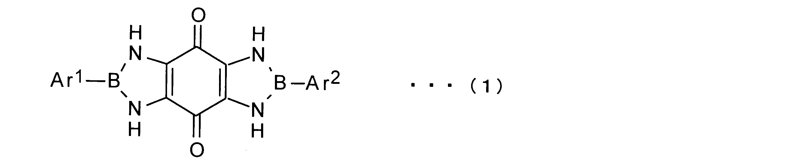
- the diazaborol compound according to claim 1 which has been made to achieve the above object, has the following chemical formula (1): (In the formula, Ar 1 and Ar 2 are the same or different and are aryl groups which may have a substituent).
- the diazaborol compound according to claim 2 is the diazaborol compound according to claim 1, wherein 80 to 100% of the hydrogen atoms of the linear, branched or cyclic alkyl group are substituted with fluorine atoms. It is a perfluoroalkyl group having 1 to 20 carbon atoms.
- the organic semiconductor material according to claim 3 has the following chemical formula (1) (Wherein, Ar 1 and Ar 2 are the same or different and are aryl groups optionally having substituents), and are characterized by containing a diazaborol compound.
- the organic semiconductor material according to claim 4 is the organic semiconductor material according to claim 3, wherein 80 to 100% of the hydrogen atoms of the linear, branched or cyclic alkyl group are substituted with fluorine atoms. And a perfluoroalkyl group having 1 to 20 carbon atoms.
- the n-type organic field effect transistor according to claim 5 is an organic semiconductor layer forming a current path between a source electrode and a drain electrode on a substrate, and a gate electrode controlling a current in the current path Are separated by an insulator layer, and the organic semiconductor layer has the following chemical formula (1) (Wherein, Ar 1 and Ar 2 are the same or different and are aryl groups optionally having substituents), and are characterized by containing a diazaborol compound.
- the diazaborol compound of the present invention has a quinone skeleton as an electron-attracting substituent in the diazaborol skeleton, and is useful as an organic semiconductor material.
- This organic semiconductor material is different from the conventionally used ⁇ -conjugated fused ring compounds, and diazaborol compounds have high solubility. It can be formed into a film.
- An n-type organic field effect transistor manufactured with this organic semiconductor material exhibits high electron mobility, can eliminate a carrier barrier, and can have a higher on / off value.
- this n-type organic field effect transistor can have a light emitting property due to the high light emission quantum efficiency of the diazaborol compound.
- 1 is an organic semiconductor layer
- 2 is a source electrode
- 3 is a drain electrode
- 5 is an insulating support substrate
- 6 is a gate electrode
- 7 is an insulator layer
- 10, 20 and 30 are organic field effect transistors
- L is a channel length. is there.
- the diazaborol compound of the present invention has the following structural formula: And a donor-acceptor type molecule comprising a diazabolol skeleton which is a donor part within a solid bracket and a quinone skeleton which is an acceptor part within a broken bracket.
- examples of the aryl group represented by Ar 1 and Ar 2 include thienyl group, furyl group, pyrrolyl group, imidazolyl group, thiazolyl group, phenyl group, biphenyl group, naphthyl group, anthryl group, phenanthryl.
- multimers consisting of one or more groups. Among them, a phenyl group, a naphthyl group, a thienyl group, and a dimer to 20mer composed of these groups are more preferable.
- substituents include a methyl group, an ethyl group, a propyl group, an isopropyl group, a butyl group, an isobutyl group, a sec-butyl group, a tert-butyl group, and a pentyl group.
- a linear or branched alkyl group such as isopentyl group, neopentyl group, tert-pentyl group, hexyl group, isohexyl group, 2-ethylhexyl group, heptyl group, octyl group, nonyl group, decyl group, dodecyl group; Group, cyclobutyl group, cyclopentyl group, cyclohexyl group, cycloheptanyl group, cyclooctanyl group, cyclononanyl group, cyclodecanyl group, cycloundecanyl group, cyclododecanyl group, etc .; trifluoromethyl group, pentafluoroethyl group Such as the straight, branched or cyclic Perfluoroalkyl group having 1 to 20 carbon atoms in which 80 to 100% of hydrogen atoms of the kill group are substituted with fluorine atom
- alkylthio groups such as methylthio group, ethylthio group, propylthio group, and butylthio group; arylthio groups such as phenylthio group and naphthylthio group; trisubstituted silyloxy groups such as tert-butyldimethylsilyloxy group and tert-butyldiphenylsilyloxy group Acetoxy group, propanoyloxy group, butanoyloxy group, pivaloyloxy group, acyloxy group such as benzoyloxy group; alkoxycarbonyl group such as methoxycarbonyl group, ethoxycarbonyl group, n-butoxycarbonyl group; methylsulfinyl group, ethylsulfinyl Alkylsulfinyl groups such as groups; arylsulfinyl groups such as phenylsulfinyl groups; methylsulfinyl
- a perfluoroalkyl group or an alkyl group is preferable.
- the alkyl group, alkoxy group and the like exemplified as the substituent have 1 to 30 carbon atoms and may be linear, branched or cyclic.
- Ar 1 and Ar 2 can have the above substituents separately, but preferably have the same substituents from the viewpoint of simplicity of the reaction operation.
- Diazaborol compounds have excellent planarity because the empty P orbitals of boron in the diazabolol skeleton are respectively supplemented by adjacent unshared electron pairs of nitrogen, and boron has a planar three-coordination type. It is.
- the diazaborol compound has a characteristic that it shows a peak in the wavelength region of 250 to 380 nm in the ultraviolet-visible absorption spectrum and has no absorption in the visible region.
- This diazaborol compound is easy to synthesize and is easily obtained.
- the diazaborol compound represented by the chemical formula (1) has the following chemical reaction formula (A), As shown in the above, 2,3,5,6-tetraaminobenzoquinone (10) and aromatic boronic acid compounds (11) and (12) are suitably synthesized by a condensation reaction.
- the aromatic boronic acid compound (11) represented by the chemical reaction formula (A) has the following structural formula: As shown in the above, a compound in which R 1 and R 2 are alkyl groups and R ′ 1 is a divalent alkylene chain may be used.
- the aromatic boronic acid compound (12) has the following structural formula: As shown by the formula, R 3 and R 4 may be an alkyl group, and R ′ 2 may be a divalent alkylene chain.
- aromatic boronic acid compounds (11) and (12) may be the same or different.
- aromatic boronic acid compounds include phenylboronic acid, methylphenylboronic acid, ethylphenylboronic acid, propylphenylboronic acid, methoxyphenylboronic acid, ethoxyphenylboronic acid, isopropyloxyphenylboronic acid, bromophenylboronic acid , Chlorophenylboronic acid, iodophenylboronic acid, fluorophenylboronic acid, difluoroboronic acid, trifluoroboronic acid, pentaphenylboronic acid, nitrophenylboronic acid, cyanophenylboronic acid, hydroxyphenylboronic acid, 4-biphenylylboronic acid 4-trifluoromethylphenylboronic acid, 4′-trifluoromethyl-4-biphenylylboronic acid, naphthylboronic acid, pyrene
- the synthesis method represented by the chemical reaction formula (A) includes 2,3,5,6-tetraaminobenzoquinone (10) and an aromatic in an inert gas atmosphere such as nitrogen or argon and in the presence of a solvent.
- the boronic acid compounds (11) and (12) are preferably reacted.
- the raw materials 2,3,5,6-tetraaminobenzoquinone (10) and the aromatic boronic acid compounds (11) and (12) are reacted at a reaction rate.
- a solvent that dissolves to such an extent that it does not hinder it is preferable.
- the solvent examples include aromatic hydrocarbons such as benzene, toluene, xylene, ethylbenzene, and mesitylene; aliphatic hydrocarbons such as pentane, hexane, heptane, octane, nonane, and decane; and alicyclic groups such as cyclohexane and cyclooctane.
- aromatic hydrocarbons such as benzene, toluene, xylene, ethylbenzene, and mesitylene
- aliphatic hydrocarbons such as pentane, hexane, heptane, octane, nonane, and decane
- alicyclic groups such as cyclohexane and cyclooctane.
- Hydrocarbons diethyl ether, diisopropyl ether, dibutyl ether, anisole, tetrahydrofuran, 1,4-dioxane and other ethers; acetonitrile, propionitrile, benzonitrile and other nitriles; methylene chloride, chloroform, carbon tetrachloride, dichloroethane, trichloroethane Halogenated hydrocarbons such as: aprotic polar solvents such as dimethyl sulfoxide and N-methylpyrrolidone; and mixed solvents thereof.
- aromatic hydrocarbons typified by toluene or ethers typified by tetrahydrofuran are preferably used.
- the amount of the solvent used is preferably 1 to 500 parts by mass, more preferably 3 to 100 parts by mass with respect to 1 part by mass of 2,3,5,6-tetraaminobenzoquinone (10). .
- the reaction temperature is preferably in the range of 0 ° C. to 200 ° C., and more preferably in the range of 50 ° C. to 200 ° C. from the viewpoint of the reaction rate.
- the reaction time varies depending on the amount ratio of 2,3,5,6-tetraaminobenzoquinone (10) and the aromatic boronic acid compounds (11) and (12) and the reaction temperature, but is 0.5 to 100 hours. It is preferable that it is the range of these.
- the diazaborol compound (1) thus obtained can be isolated and purified by a method usually performed in the isolation and purification of organic compounds.
- a method usually performed in the isolation and purification of organic compounds For example, when the target product is precipitated as a solid in the reaction mixture, it can be filtered as it is. When the target product is not precipitated, the reaction mixture can be concentrated as it is to precipitate a solid, and the target product can be obtained by filtration.
- a diazaborol compound (1) having a high purity can be obtained.
- diazaborol compounds can be used as organic semiconductor materials with n-type characteristics having high electron transfer and on / off values.
- an n-type organic field effect transistor can be manufactured by using the organic semiconductor material containing the diazaborol compound of the present invention for the organic semiconductor layer.
- An n-type organic field effect transistor is formed by laminating a gate electrode layer to which a voltage is applied, an insulator layer, an organic semiconductor layer, and a source-drain electrode layer serving as a current path on a substrate. is there.
- the n-type organic field effect transistor 10 includes a gate electrode 6, an insulator layer 7, an organic semiconductor layer 1 containing a diazaborol compound, a source electrode 2 and a drain on an insulating support substrate 5.
- a source-drain electrode layer 2-3 composed of the electrode 3 is sequentially laminated to form a bottom gate / top contact type.
- the gate electrode 6 controls the current flowing in the current path, and is isolated from the organic semiconductor layer 1 and the source-drain electrode layer 2-3 by the insulator layer 7.
- the source-drain electrode layer 2-3 is deposited on the organic semiconductor layer 1 and forms a channel region that becomes a current path between the source electrode 2 and the drain electrode 3.
- the n-type organic field effect transistor 10 generates an electric field when a voltage is applied to the gate electrode 6, and forms a channel region serving as a current path between the source electrode 2 and the drain electrode 3 in the source-drain electrode layer 2-3. To do. In the source-drain electrode layer 2-3 and the organic semiconductor layer 1, electrons are supplied from the source electrode 2 to the organic semiconductor layer 1, and electrons are discharged from the organic semiconductor layer 1 to the drain electrode 3. Current flows. The transistor operation is performed by changing the carrier density of the organic semiconductor layer 1 and the insulator layer 7 and changing the amount of current flowing between the source electrode 2 and the drain electrode 3.
- the organic semiconductor layer 1 is formed by forming a film using the diazaborol compound of the present invention or an organic semiconductor material containing the compound.
- the organic semiconductor layer 1 is an electron transfer layer for moving electrons as carriers from one electrode to the other electrode.
- the film thickness of the organic semiconductor layer 1 is preferably about 1 nm to 10 ⁇ m, and more preferably about 10 to 500 nm.
- raw materials for the insulating support substrate 5 include polyethylene terephthalate (PET), glass, quartz, silicon, ceramics, and plastics.
- the thickness of the insulating support substrate 5 is preferably about 0.05 to 2 mm, and more preferably about 0.1 to 1 mm.
- the insulator layer 7 preferably has an electric conductivity at room temperature having a leak current of 10 ⁇ 2 A / cm 2 or less under an electric field strength of 1.0 MV / cm. Further, the relative dielectric constant is usually about 4.0, and it is preferable that the relative dielectric constant shows a high value.
- the raw material for the insulator layer 7 include silicon oxide, silicon nitride, amorphous silicon, aluminum oxide, and tantalum oxide.
- the group consisting of polystyrene, polyvinylphenol, polycarbonate, polyester, polyvinyl acetate, polyurethane, polysulfone, (meth) acrylic resin, epoxy resin, hydrocarbon resin and phenol resin having cyano group, polyimide resin and polyparaxylylene resin You may form from the resin or resin composition which has 1 type, or 2 or more types of resin selected from these as a main component.
- the film thickness of the insulator layer 7 is preferably about 50 nm to 2 ⁇ m, more preferably about 100 nm to 1 ⁇ m.
- the raw materials to be the gate electrode 6, the source electrode 2, and the drain electrode 3 are not particularly limited as long as they exhibit conductivity. Specifically, platinum, gold, silver, nickel, chromium, copper, iron, tin, antimony lead, tantalum, indium, palladium, tellurium, rhenium, iridium, aluminum, ruthenium, germanium, molybdenum, tungsten, tin oxide / antimony, Indium tin oxide (ITO), fluorine-doped zinc oxide, zinc, silicon, carbon, graphite, classy carbon, silver paste and carbon paste, lithium, beryllium, sodium, magnesium, potassium, calcium, scandium, titanium, manganese, zirconium, Gallium, niobium, sodium-potassium alloy, magnesium / silver mixture, magnesium / silver mixture, magnesium / aluminum mixture, magnesium / indium mixture, aluminum / aluminum oxide Mixture, lithium / aluminum mixture, amorphous silicon, and the like.
- a known conductive polymer whose conductivity is improved by doping or the like for example, conductive polyaniline, conductive polypyrrole, conductive polythiophene, a complex of polyethylenedioxythiophene and polystyrenesulfonic acid, or the like is also preferably used.
- the film thicknesses of the gate electrode 6, the source electrode 2, and the drain electrode 3 are preferably 0.01 to 2 ⁇ m, and more preferably 0.2 to 1 ⁇ m.
- the channel length L which is the distance between the source electrode 2 and the drain electrode 3, is usually 100 ⁇ m or less and preferably 50 ⁇ m or less.
- the channel width W is usually 2000 ⁇ m or less and preferably 500 ⁇ m or less.
- L / W is usually 0.1 or less and preferably 0.05 or less.
- the method for forming the n-type organic field effect transistor 10 is not particularly limited, and a conventionally known method can be used.
- the organic semiconductor layer 1 can be formed by dissolving a diazabolol compound in a solvent to form a solution and applying it by a casting method, a dip method, a spin coating method, or a vacuum deposition method.
- the insulator layer 7 can be formed by, for example, a coating method such as spin coating or blade coating, a vapor deposition method, a sputtering method, a printing method such as screen printing, an inkjet method, or an electrostatic charge image developing method.
- a photo-curing resin that forms an insulator by applying a monomer as a precursor of the insulator and then curing it by irradiation with light may be used.
- the gate electrode 6, the source electrode 2, and the drain electrode 3 can be formed by, for example, a vacuum deposition method, a sputtering method, a coating method, a printing method, a sol-gel method, or the like.
- these patterning methods there are a photolithography method, a printing method such as inkjet printing, screen printing, offset printing, letterpress printing, a soft lithography method such as a micro contact printing method, and a method combining a plurality of these methods. Can be mentioned.
- it can also form by the method of irradiating energy rays, such as a laser and an electron beam, and removing a material.
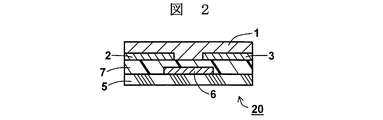
- the n-type organic field effect transistor 20 includes a gate electrode 6, an insulator layer 7, a source-drain electrode layer 2-3 that is a source electrode 2 and a drain electrode 3, and an organic semiconductor layer 1 on an insulating substrate 5. Is a bottom-gate / bottom-contact type formed by sequentially laminating. Except for the difference in the channel region due to the difference in the arrangement of the source-drain electrode layer 2-3 and the organic semiconductor layer 1, it is the same as that shown in FIG.
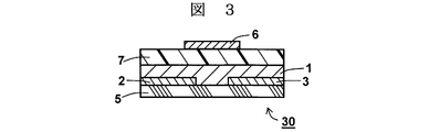
- FIG. 3 shows an example of yet another n-type organic field effect transistor 30.
- the n-type organic field effect transistor 30 has a top-gate / bottom in which a source-drain electrode layer 2-3, an organic semiconductor layer 1, an insulator layer 7, and a gate electrode 6 are sequentially formed on an insulating substrate 5. Contact type.
- the structure of the n-type organic field effect transistor is not particularly limited.
- a protective film is formed on the organic semiconductor layer 1. It may be what you are doing. This protective film can minimize the influence of outside air on the organic semiconductor layer 1.
- the raw material of the protective film include polymers such as epoxy resin, acrylic resin, polyurethane, polyimide, and polyvinyl alcohol, and inorganic oxides and nitrides such as silicon oxide, silicon nitride, and aluminum oxide.
- the protective film can be formed by a coating method, a vacuum deposition method, or the like.
- the solid obtained by filtration was washed with water, mixed with 80% hydrazine aqueous solution (200 ml), and heated and stirred at 70 to 80 ° C. for 1 hour.
- the reaction solution was filtered while hot, washed with water and diethyl ether, and then dried under reduced pressure to obtain 4.96 g (yield: 59%) of 2,3,5,6-tetraaminobenzoquinone as a purple solid. It was.
- IR infrared absorption analysis
- Mass spectrometry 340 [M + ]. Elemental analysis (C 18 H 14 B 2 N 4 O 2): Calculated Value (%) C: 63.60, H: 4.15, B: 6.36, N: 16.48, O: 9.41; Actual value (%) C: 61.38, H: 4.16, N: 15.86 IR (KBr, cm ⁇ 1 ): 569, 633, 691, 746, 992, 1004, 1017, 1148, 1247, 1344, 1402, 1439, 1505, 1565, 1621, 3341, 3464.
- Example 2 4-biphenylylboronic acid (2.0 g, 10 mmol), 2,3,5,6-tetraaminobenzoquinone (282 mg, 1.7 mmol), toluene (150 ml) were added to a 300 ml eggplant-shaped flask, The mixture was heated and stirred for 48 hours. The reaction solution was filtered while hot, and the resulting solid was dried under reduced pressure and purified by sublimation to obtain 113 mg (yield: 20%) of a compound represented by the following chemical formula (3).
- Example 3 In a 300 ml eggplant-shaped flask, 4- (4-trifluoromethyl) phenylboronic acid (2.0 g, 10.5 mmol), 2,3,5,6-tetraaminobenzoquinone (354 mg, 2.1 mmol), toluene (150 ml) ) was added, and the mixture was heated and stirred for 48 hours under reflux conditions. The reaction solution was filtered while hot, and the obtained solid was dried under reduced pressure and purified by sublimation to obtain 544 mg (yield: 54%) of a compound represented by the following chemical formula (4).
- Example 4 In a 300 ml eggplant-shaped flask, 4- (4-trifluoromethylphenyl) phenylboronic acid (380 mg, 1.4 mmol), 2,3,5,6-tetraaminobenzoquinone (94 mg, 0.56 mmol), toluene (150 ml) And heated and stirred for 48 hours under reflux conditions. The reaction solution was filtered while hot, and the obtained solid was dried under reduced pressure and purified by sublimation to obtain 27.8 mg (yield: 10%) of a compound represented by the following chemical formula (5).
- Example 5 4-Hexylphenylboronic acid (1.0 g, 4.9 mmol), 2,3,5,6-tetraaminobenzoquinone (244 mg, 1.45 mmol) and toluene (150 ml) were added to a 300 ml eggplant-shaped flask under reflux conditions. Under stirring for 48 hours. The reaction solution was filtered while hot, and the obtained solid was dried under reduced pressure and purified by sublimation to obtain 86 mg (yield: 12%) of a compound represented by the following chemical formula (6).
- Example 6 Top Contact Type-n Type Organic Field Effect Transistor
- a silicon wafer having a thickness of 500 ⁇ m was cut into a size of 3.5 ⁇ 2.5 cm, and this wafer was used as the insulating support substrate 5.
- the substrate was treated with ozone, or after treatment with hexamethyldisilazane (HMDS) or octyltrichlorosilane (OTS).
- HMDS hexamethyldisilazane
- OTS octyltrichlorosilane
- An n-type silicon wafer was formed on this processing substrate, and this was used as the gate electrode 6.
- a 200 nm silicon oxide (SiO 2 ) insulator layer 7 was formed on the gate electrode by thermal oxidation.
- the compound obtained in Examples 1, 2, and 4 was deposited by 30 nm on the SiO 2 using a vacuum deposition method to form the organic semiconductor layer 1. Further, gold was deposited in a thickness of 50 nm on the organic semiconductor layer 1 using a vacuum deposition method (2 and 3) to obtain a top contact type n-type organic field effect transistor shown in FIG. The deposition was performed so that the channel length (L) was 50, 75 and 100 ⁇ m, and the channel width (W) was 1000 ⁇ m.
- n-type organic field effect transistor using an electrometer, a voltage of 10 to 60 V was applied between the source electrode and the drain electrode, and the gate voltage was changed in the range of ⁇ 20 to 100 V, so that the voltage-current A curve was obtained at a temperature of 25 ° C., and the transistor characteristics were evaluated. Transistor characteristics were observed only for positive bias. This means that the obtained field effect transistor is an n-type organic field effect transistor.
- the field effect mobility ( ⁇ ) was calculated using the following formula (C) representing the drain current Id.
- Id (W / 2L) ⁇ ⁇ ⁇ Ci ⁇ (Vg ⁇ Vt) 2 (C)
- L is the gate length and W is the gate width.
- Ci is a capacitance per unit area of the insulating layer, Vg is a gate voltage, and Vt is a threshold voltage.
- the on / off ratio was calculated from the ratio between the maximum and minimum drain current values (Id).
- the obtained transistor characteristic evaluation results are shown in Table 1.
- Example 7 Bottom Contact Type-n Type Organic Field Effect Transistor Comb-shaped electrodes (2 and 3) were formed on the silicon oxide insulator layer 7 (thickness: 300 nm) formed in the same manner as in Example 6 by using a photolithography method.
- the electrode layer structure chromium (Cr) was vapor-deposited on silicon oxide to a film thickness of 10 nm, and gold was vapor-deposited thereon to a film thickness of 20 nm.
- the comb pattern was such that the electrode channel length was 25 ⁇ m and the channel width was 294 ⁇ m (6 ⁇ m ⁇ 49).
- Examples 2 to 5 were carried out on the silicon oxide insulator layer 7 on which the electrodes (2 and 3) were formed, at a substrate temperature of room temperature or 50 ° C. under a vacuum of 10 ⁇ 5 Pa and at a deposition rate of 0.1 to 0.3 mm.
- the organic semiconductor layer 1 was formed by vapor-depositing the compound obtained in 50 nm to obtain a bottom contact type n-type organic field effect transistor shown in FIG. In the case of the coating method, a chloroform solution was dropped on a substrate to form a film.
- top indicates the top contact type
- bottom indicates the bottom contact type
- HMDS which is the notation of the substrate processing, indicates that the treatment is performed with hexamethyldisilazane.
- the diazaborol compound of the present invention is used as an organic semiconductor material for an organic field effect transistor.
Landscapes
- Chemical & Material Sciences (AREA)
- Organic Chemistry (AREA)
- Physics & Mathematics (AREA)
- Spectroscopy & Molecular Physics (AREA)
- Engineering & Computer Science (AREA)
- Materials Engineering (AREA)
- Thin Film Transistor (AREA)
Abstract
有機半導体材料に有用であるジアザボロール化合物、およびそれを含有している有機半導体材料から塗布法や印刷法により簡便に有機半導体層を製膜でき、高い電子移動度と電流オン/オフ比とを示すn型有機電界効果トランジスタを提供する。 ジアザボロール化合物は、下記化学式(1)(式中、Ar1およびAr2は、同一または異なり、置換基を有していてもよいアリール基である)で表されるものである。n型有機電界効果トランジスタは、基板上で、ソース電極およびドレイン電極の間の電流路を形成している有機半導体層と、前記電流路の電流を制御しているゲート電極とが、絶縁体層で隔離されており、前記有機半導体層に、このジアザボロール化合物を含有しているものである。
Description
本発明は、有機半導体材料に有用であるジアザボロール化合物、およびその化合物を電子移動層とするn型有機電界効果トランジスタに関する。
電界効果トランジスタは、一種類のキャリアを用いるユニポーラトランジスタの一つであり、重要なスイッチング素子や増幅素子として広く利用されているものである。その構造は、ソース電極およびドレイン電極の間の電流路を形成している半導体層と、ゲート電圧を印加して電流の流れを制御するゲート電極からその半導体層を隔離している絶縁体層とで構成されている。
この電界効果トランジスタの特性は、半導体の移動度およびオン/オフ値が重要であり、用いられる半導体、なかでも半導体材料の特性により決まる。
従来から、アモルファスシリコンやポリシリコンなどの無機材料が半導体材料として汎用的に用いられてきた。このようなシリコンに代表される無機半導体では、高温処理されるため、電界効果トランジスタの基板としてプラスチック基板やプラスチックフィルムを用いることが困難となる。また、真空における素子作製工程を経るため、高価な製造設備を必要とし、コスト高となる。
近年では、無機半導体に換え、有機半導体を使用した有機電界効果トランジスタが注目されており、基本的な光電子工学の観点から有機半導体材料の研究が進められている。この有機電界効果トランジスタは、有機半導体を使用することで、軽量化、フレキシブル化、大面積化が可能になるとともに、製造工程が簡易なものとなる。また、溶媒に可溶な高溶解性の有機化合物を用いることで、塗布法やインクジェット等の印刷法を用いて有機半導体を製膜し、有機電界効果トランジスタを製造することが可能となる。
有機半導体材料は、正の電荷を有する正孔が電流を伝える役割を担う半導体であるp型有機半導体として多数開発されてきている。既に本発明者は、3配位型ホウ素原子を含有する複素環化合物を有機半導体材料とし、有機電子デバイスを作成している(非特許文献1)。これらの化合物を有機半導体とした有機電界効果トランジスタは、p型特性を示し、実用レベルの優れた正孔移動度を有する。
一方、負の電荷を有する自由電子が電流を伝える役割を担う半導体であるn型有機半導体としては、バリエーションが少ない現状である。例えば特許文献1に、1つ以上のフッ素原子を有する置換基を少なくとも1つ有するグラフェン誘導体であるn型の有機半導体材料が開示されている。電子求引基であるフッ素原子を有する官能基を導入することで、グラフェン骨格の特性を有したn型半導体の材料として利用することができる。その他、n型特性を示す半導体材料として、フタロシアニン誘導体やフラーレン誘導体も用いられている。
しかし、これらのn型特性を示す材料は、溶解性が低いこと、合成が難しいこと、電子移動度が不十分であることなどの問題があり、実用性に乏しい。
山下 敬郎(Yoshiro Yamashita)ら、ケミストリー レターズ(Chemistry Letters)、2008年、第37巻、第11号、p.1122
本発明は前記の課題を解決するためになされたもので、有機半導体材料に有用であるジアザボロール化合物、およびそれを含有している有機半導体材料から塗布法や印刷法により簡便に有機半導体層を製膜でき、高い電子移動度とオン/オフ値とを示すn型有機電界効果トランジスタを提供することを目的とする。
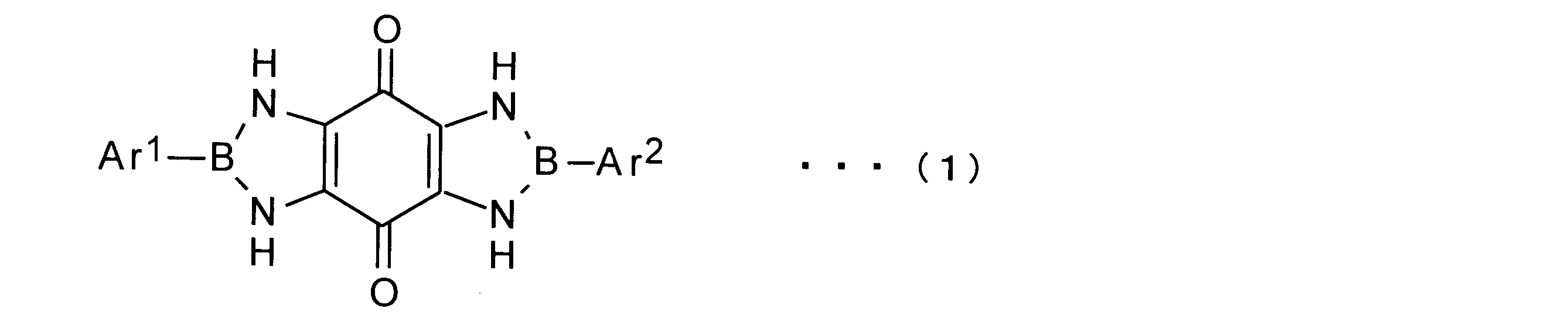
前記の目的を達成するためになされた、請求の範囲の請求項1に記載されたジアザボロール化合物は、下記化学式(1)

(式中、Ar1およびAr2は、同一または異なり、置換基を有していてもよいアリール基である)で表されることを特徴とする。
請求項2に記載のジアザボロール化合物は、請求項1に記載されたものであって、前記置換基が、直鎖、分岐または環状アルキル基の水素原子のうち80~100%がフッ素原子で置換された炭素数1~20のパーフルオロアルキル基であることを特徴とする。
請求項3に記載の有機半導体材料は、下記化学式(1)

(式中、Ar1およびAr2は、同一または異なり、置換基を有していてもよいアリール基である)で表されるジアザボロール化合物を含有していることを特徴とする。
請求項4に記載の有機半導体材料は、請求項3に記載されたものであって、前記置換基が、直鎖、分岐または環状アルキル基の水素原子のうち80~100%がフッ素原子で置換された炭素数1~20のパーフルオロアルキル基であることを特徴とする。
請求項5に記載のn型有機電界効果トランジスタは、基板上で、ソース電極およびドレイン電極の間の電流路を形成している有機半導体層と、前記電流路の電流を制御しているゲート電極とが、絶縁体層で隔離されており、前記有機半導体層に、下記化学式(1)
(式中、Ar1およびAr2は、同一または異なり、置換基を有していてもよいアリール基である)で表されるジアザボロール化合物を含有していることを特徴とする。
本発明のジアザボロール化合物は、そのジアザボロール骨格に電子求引性の置換基となるキノン骨格を有しており、有機半導体材料として有用である。
この有機半導体材料は、従来用いられてきたπ共役系にみられるような縮環化合物と異なり、ジアザボロール化合物が高い溶解性を有するため、蒸着法だけでなく塗布法やインクジェット等の印刷法により簡便に製膜することができる。
この有機半導体材料で製造したn型有機電界効果トランジスタは、高い電子移動度を示し、キャリア障壁を解消することができ、さらに高いオン/オフ値を有することができる。
またこのn型有機電界効果トランジスタは、ジアザボロール化合物の高い発光量子効率による発光性を有することができる。
1は有機半導体層、2はソース電極、3はドレイン電極、5は絶縁性支持基板、6はゲート電極、7は絶縁体層、10,20,30は有機電界効果トランジスタ、Lはチャネル長である。
以下、本発明を実施するための形態を詳細に説明するが、本発明の範囲はこれらの形態に限定されるものではない。
本発明のジアザボロール化合物は、下記構造式、
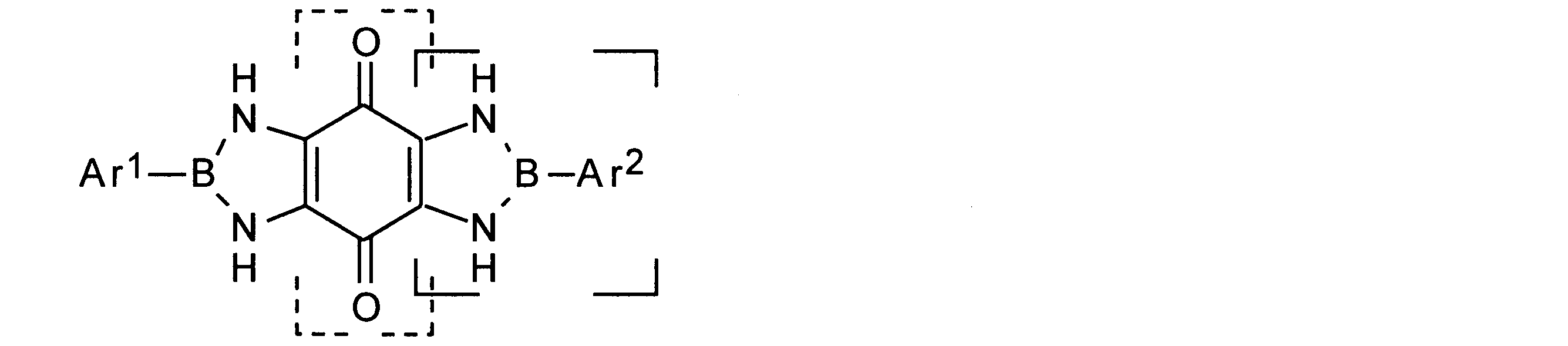
で表わされ、実線鉤括弧内のドナー部であるジアザボロール骨格と、破線鉤括弧内のアクセプター部であるキノン骨格とからなるドナー・アクセプター型分子である。
前記化学式(1)において、Ar1、Ar2で表わされるアリール基としては、例えば、チエニル基、フリル基、ピロリル基、イミダゾリル基、チアゾリル基、フェニル基、ビフェニル基、ナフチル基、アントリル基、フェナントリル基、フルオレニル基、カルバゾリル基、イミダゾリル基、ピリジル基、キノリル基、ベンズオキサゾリル基、ベンズイミダゾリル基、ベンズチアゾリル基、カルバゾリル基、アゼピニル基などが挙げられ、さらには前記のアリール基の任意の一つまたは複数の基からなる多量体も挙げられる。それらの中でも、フェニル基、ナフチル基、チエニル基およびそれらの基からなる2~20量体がより好ましい。
これらは置換基を有していてもよく、かかる置換基としては、例えば、メチル基、エチル基、プロピル基、イソプロピル基、ブチル基、イソブチル基、sec-ブチル基、tert-ブチル基、ペンチル基、イソペンチル基、ネオペンチル基、tert-ペンチル基、ヘキシル基、イソヘキシル基、2-エチルヘキシル基、ヘプチル基、オクチル基、ノニル基、デシル基、ドデシル基等の直鎖や分岐鎖のアルキル基;シクロプロピル基、シクロブチル基、シクロペンチル基、シクロヘキシル基、シクロヘプタニル基、シクロオクタニル基、シクロノナニル基、シクロデカニル基、シクロウンデカニル基、シクロドデカニル基等のシクロアルキル基;トリフルオロメチル基、ペンタフルオロエチル基などの、上記した直鎖、分岐または環状アルキル基の水素原子のうち80~100%がフッ素原子で置換された炭素数1~20のパーフルオロアルキル基;フェニル基、ナフチル基、アントリル基、フェナントリル基等のアリール基;ピリジル基、チエニル基、フリル基、ピロリル基、イミダゾリル基、ピラジニル基、オキサゾリル基、チアゾリル基、ピラゾリル基、ベンゾチアゾリル基、ベンゾイミダゾリル基等の複素芳香環基;メトキシ基、エトキシ基、プロポキシ基、イソプロポキシ基、ブトキシ基、イソブトキシ基、sec-ブトキシ基、tert-ブトキシ基、ペンチルオキシ基、イソペンチルオキシ基、ネオペンチルオキシ基、ヘキシルオキシ基、シクロヘキシルオキシ基、ヘプチルオキシ基、オクチルオキシ基、ノニルオキシ基、デシルオキシ基、ドデシルオキシ基等のアルコキシ基;メチルチオ基、エチルチオ基、プロピルチオ基、ブチルチオ基等のアルキルチオ基;フェニルチオ基、ナフチルチオ基等のアリールチオ基;tert-ブチルジメチルシリルオキシ基、tert-ブチルジフェニルシリルオキシ基等の三置換シリルオキシ基;アセトキシ基、プロパノイルオキシ基、ブタノイルオキシ基、ピバロイルオキシ基、ベンゾイルオキシ基などのアシロキシ基;メトキシカルボニル基、エトキシカルボニル基、n-ブトキシカルボニル基などのアルコキシカルボニル基;メチルスルフィニル基、エチルスルフィニル基等のアルキルスルフィニル基;フェニルスルフィニル基等のアリールスルフィニル基;メチルスルフォニルオキシ基、エチルスルフォニルオキシ基、フェニルスルフォニルオキシ基、メトキシスルフォニル基、エトキシスルフォニル基、フェニルオキシスルフォニル基等のスルフォン酸エステル基;ジメチルアミノ基、ジフェニルアミノ基、メチルフェニルアミノ基、メチルアミノ基、エチルアミノ基などの1級または2級のアミノ基;アセチル基、ベンゾイル基、ベンゼンスルホニル基、tert-ブトキシカルボニル基などで置換された、メチル基、エチル基、プロピル基、イソプロピル基、ブチル基、イソブチル基、tert-ブチル基、フェニル基などのアルキル基またはアリール基などで置換されていてもよいアミノ基;シアノ基;ニトロ基;フッ素原子、塩素原子、臭素原子、ヨウ素原子等のハロゲン原子;などが挙げられる。前記の置換基の中では、パーフルオロアルキル基またはアルキル基が好ましい。前記置換基として例示したアルキル基やアルコキシ基等は、炭素数1~30であり、直鎖状であってもよく、分岐状または環状であってもよい。
Ar1およびAr2は、前記の置換基を別々に有することができるが、反応操作の簡便性の観点から、同じ置換基を有することが好ましい。
ジアザボロール化合物は、そのジアザボロール骨格中のホウ素の有する空のP軌道を、隣接する窒素の非共有電子対によりそれぞれ補っており、ホウ素が平面3配位型となるため、優れた平面性を示すものである。また、ジアザボロール化合物は、紫外可視吸収スペクトルにおいて、250~380nmの波長領域にピークを示し、可視領域に吸収を持たない特性を有する。
このジアザボロール化合物は、その合成反応が容易であり、簡便に得られるものである。
ジアザボロール化合物の製造方法を以下に示す。
前記化学式(1)で表わされるジアザボロール化合物は、下記化学反応式(A)、
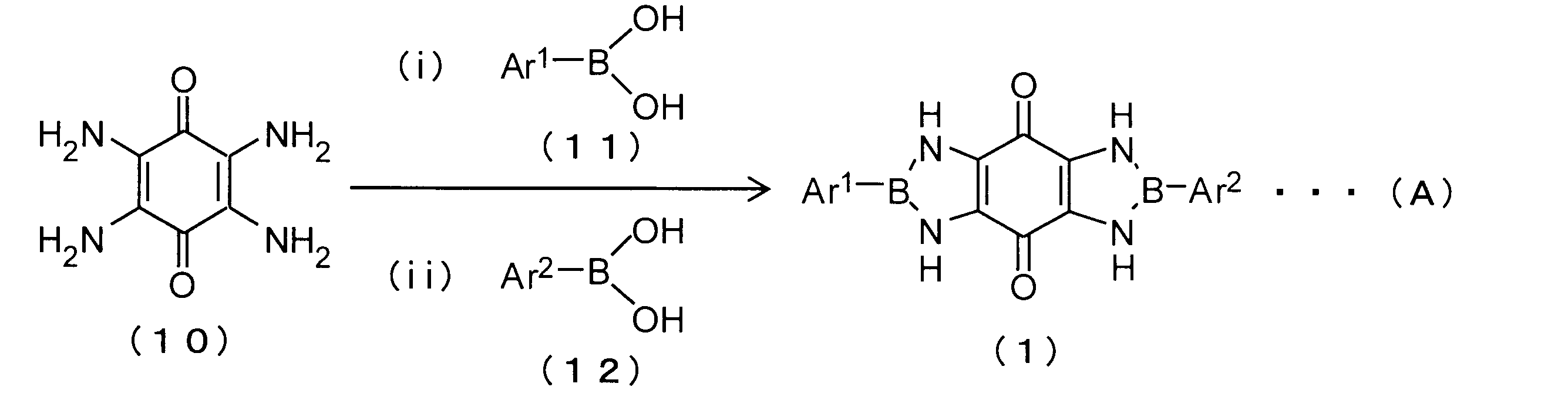
で示されるように、2,3,5,6-テトラアミノベンゾキノン(10)と、芳香族ボロン酸化合物(11)および(12)とを、縮合反応させることにより好適に合成される。
前記化学反応式(A)で示される芳香族ボロン酸化合物(11)は、下記構造式、

で示されるように、R1およびR2がアルキル基であり、R’1が2価のアルキレン鎖である化合物であってもよい。
同様に、芳香族ボロン酸化合物(12)は、下記構造式、

で示されるように、R3およびR4がアルキル基であり、R’2が2価のアルキレン鎖である化合物であってもよい。
芳香族ボロン酸化合物(11)および(12)は、同一であってもよく、異なっていてもよい。芳香族ボロン酸化合物として、具体的に、フェニルボロン酸、メチルフェニルボロン酸、エチルフェニルボロン酸、プロピルフェニルボロン酸、メトキシフェニルボロン酸、エトキシフェニルボロン酸、イソプロピルオキシフェニルボロン酸、ブロモフェニルボロン酸、クロロフェニルボロン酸、ヨードフェニルボロン酸、フルオロフェニルボロン酸、ジフルオロボロン酸、トリフルオロボロン酸、ペンタフェニルボロン酸、ニトロフェニルボロン酸、シアノフェニルボロン酸、ヒドロキシフェニルボロン酸、4-ビフェニリルボロン酸、4-トリフルオロメチルフェニルボロン酸、4’-トリフルオロメチル-4-ビフェニリルボロン酸、ナフチルボロン酸、ピレンボロン酸、ピリジンボロン酸、キノリンボロン酸、インドールボロン酸、チオフェンボロン酸、フランボロン酸、ベンゾフランボロン酸、ベンゾ[b]チオフェンボロン酸などが挙げられる。
前記化学反応式(A)で示される合成方法は、窒素、アルゴンなどの不活性ガス雰囲気下、および溶媒の存在下において、2,3,5,6-テトラアミノベンゾキノン(10)と、芳香族ボロン酸化合物(11)および(12)とを反応させると好ましい。
前記化学反応式(A)において、用いられる溶媒としては、原料である2,3,5,6-テトラアミノベンゾキノン(10)と芳香族ボロン酸化合物(11)および(12)とが反応速度に支障をきたさない程度に溶解する溶媒であることが好ましい。
かかる溶媒としては、例えば、ベンゼン、トルエン、キシレン、エチルベンゼン、メシチレンなどの芳香族炭化水素;ペンタン、ヘキサン、ヘプタン、オクタン、ノナン、デカンなどの脂肪族炭化水素;シクロヘキサン、シクロオクタンなどの脂環式炭化水素;ジエチルエーテル、ジイソプロピルエーテル、ジブチルエーテル、アニソール、テトラヒドロフラン、1,4-ジオキサンなどのエーテル;アセトニトリル、プロピオニトリル、ベンゾニトリルなどのニトリル類;塩化メチレン、クロロホルム、四塩化炭素、ジクロロエタン、トリクロロエタンなどのハロゲン化炭化水素類;ジメチルスルホキシド、N-メチルピロリドンなどの非プロトン性極性溶媒;およびこれらの混合溶媒などが挙げられる。これらの中でも、トルエンに代表される芳香族炭化水素またはテトラヒドロフランに代表されるエーテルが好適に用いられる。
かかる溶媒の使用量は、2,3,5,6-テトラアミノベンゾキノン(10)1質量部に対して、1~500質量部であることが好ましく、3~100質量部であることがより好ましい。
反応温度は、0℃~200℃の範囲であるのが好ましく、反応速度の観点から50℃~200℃の範囲であるのがより好ましい。
反応時間は、2,3,5,6-テトラアミノベンゾキノン(10)と芳香族ボロン酸化合物(11)および(12)との使用量比ならびに反応温度によっても異なるが、0.5~100時間の範囲であるのが好ましい。
このようにして得られたジアザボロール化合物(1)は、有機化合物の単離・精製において通常行われる方法により単離・精製することができる。例えば、反応混合液に目的物が固体として析出している場合は、そのままろ過することができる。また、目的物が析出していない場合は、反応混合液をそのまま濃縮して固体を析出させ、ろ過により目的物を得ることができる。このようにして得られた目的物を、必要に応じて昇華、再結晶、蒸留、シリカゲルカラムクロマトグラフィーなどで精製することで、純度の高いジアザボロール化合物(1)を得ることができる。
これらのジアザボロール化合物は、高い電子移動およびオン/オフ値を有するn型特性の有機半導体材料として用いることができる。
さらに、本発明のジアザボロール化合物を含有している有機半導体材料を有機半導体層に用いることで、n型有機電界効果トランジスタを製造することができる。
n型有機電界効果トランジスタは、基板上で、電圧が印加されるゲート電極層と、絶縁体層と、有機半導体層と、電流路となるソース-ドレイン電極層とが、積層されているものである。それらの各層の積層配置の違いにより、ボトムゲート・トップコンタクト型、ボトムゲート・ボトムコンタクト型、トップゲート・ボトムコンタクト型、およびトップゲート・トップコンタクト型がある。
n型有機電界効果トランジスタの好ましい一実施例について、図1を参照しながら、詳細に説明する。
n型有機電界効果トランジスタ10は、図1に示す通り、絶縁性支持基板5上に、ゲート電極6、絶縁体層7、ジアザボロール化合物を含有している有機半導体層1、およびソース電極2とドレイン電極3とからなるソース-ドレイン電極層2-3が、順次積層されて、ボトムゲート・トップコンタクト型を形成している。ゲート電極6は、電流路に流れる電流を制御しており、絶縁体層7によって有機半導体層1およびソース-ドレイン電極層2-3から隔離されている。ソース-ドレイン電極層2-3は、有機半導体層1に蒸着されており、ソース電極2およびドレイン電極3の間の電流路となるチャネル領域を形成している。
n型有機電界効果トランジスタ10は、ゲート電極6に電圧を印加すると電界が生じ、ソース-ドレイン電極層2-3において、ソース電極2とドレイン電極3との間で電流路となるチャネル領域を形成する。そのソース-ドレイン電極層2-3と有機半導体層1とにおいて、ソース電極2から有機半導体層1へ電子の供給が行われ、また有機半導体層1からドレイン電極3へ電子の排出が行われ、電流が流れる。有機半導体層1と絶縁体層7のキャリア密度を変化させ、ソース電極2およびドレイン電極3の間に流れる電流量を変化させることで、トランジスタ動作が行われる。
有機半導体層1は、本発明のジアザボロール化合物、またはそれを含有している有機半導体材料を用いて製膜し、形成されているものである。有機半導体層1は、一方の電極からもう一方の電極へ、キャリアである電子を移動させるための電子移動層である。
有機半導体層1の膜厚は、1nm~10μm程度であると好ましく、10~500nm程度であるとより好ましい。
絶縁性支持基板5となる原材料として、具体的に、ポリエチレンテレフタレート(PET)、ガラス、石英、シリコン、セラミックス、プラスチック等が挙げられる。
絶縁性支持基板5の厚みは、0.05~2mm程度であると好ましく、0.1~1mm程度であるとより好ましい。
絶縁体層7は、室温における電気伝導度が、1.0MV/cmの電界強度下においてリーク電流が10-2A/cm2以下のものであると好ましい。また、その比誘電率は、通常で4.0程度であり、高い値を示すものであると好ましい。
絶縁体層7となる原材料として、具体的に、酸化シリコン、窒化シリコン、アモルファスシリコン、酸化アルミニウム、酸化タンタル等が挙げられる。また、ポリスチレン、ポリビニルフェノール、ポリカーボネート、ポリエステル、ポリ酢酸ビニル、ポリウレタン、ポリスルホン、(メタ)アクリル樹脂、エポキシ樹脂、シアノ基を有する炭化水素樹脂およびフェノール樹脂、ポリイミド樹脂およびポリパラキシリレン樹脂からなる群から選択される1種または2種以上の樹脂を主成分とする樹脂または樹脂組成物から形成してもよい。
絶縁体層7の膜厚は、好ましくは50nm~2μm程度であり、更に好ましくは100nm~1μm程度である。
ゲート電極6、ソース電極2およびドレイン電極3となる原材料は、特に制限されず導電性を示すものであればよい。具体的に、白金、金、銀、ニッケル、クロム、銅、鉄、錫、アンチモン鉛、タンタル、インジウム、パラジウム、テルル、レニウム、イリジウム、アルミニウム、ルテニウム、ゲルマニウム、モリブデン、タングステン、酸化スズ・アンチモン、酸化インジウム・スズ(ITO)、フッ素ドープ酸化亜鉛、亜鉛、シリコン、炭素、グラファイト、クラッシーカーボン、銀ペーストおよびカーボンペースト、リチウム、ベリリウム、ナトリウム、マグネシウム、カリウム、カルシウム、スカンジウム、チタン、マンガン、ジルコニウム、ガリウム、ニオブ、ナトリウム-カリウム合金、マグネシウム/銀混合物、マグネシウム/銀混合物、マグネシウム/アルミニウム混合物、マグネシウム/インジウム混合物、アルミニウム/酸化アルミニウム混合物、リチウム/アルミニウム混合物、アモルファスシリコン等が挙げられる。また、ドーピング等で導電率を向上させた、公知の導電性ポリマー、例えば、導電性ポリアニリン、導電性ポリピロール、で導電性ポリチオフェン、ポリエチレンジオキシチオフェンとポリスチレンスルホン酸の錯体等も好適に用いられる。
ゲート電極6、ソース電極2、ドレイン電極3の膜厚は、0.01~2μmであると好ましく、0.2~1μmであるとより好ましい。
また、ソース電極2およびドレイン電極3の間の距離であるチャネル長Lは、通常では100μm以下であり、50μm以下であると好ましい。一方、チャネル幅Wは、通常では2000μm以下であり、500μm以下であると好ましい。L/Wは、通常では0.1以下であり、0.05以下であると好ましい。
n型有機電界効果トランジスタ10を形成する方法は、特に制限なく、従来公知の方法を用いることができる。
有機半導体層1は、ジアザボロール化合物を溶媒に溶解して溶液とし、キャスト法、ディップ法、スピンコート法等により塗布する方法や、真空蒸着法等により製膜することができる。
絶縁体層7は、例えば、スピンコートやブレードコート等の塗布法、蒸着法、スパッタ法、スクリーン印刷やインクジェットや静電荷像現像方法等の印刷法等により形成することができる。また、絶縁体の前駆物質としてモノマーを塗布した後、光を照射して硬化させることにより絶縁体を形成する光硬化樹脂を用いてもよい。
ゲート電極6、ソース電極2およびドレイン電極3は、例えば、真空蒸着法、スパッタ法、塗布法、印刷法、ゾルゲル法等により形成することができる。更に、それらのパターニング法としては、フォトリソグラフィー法、インクジェット印刷、スクリーン印刷、オフセット印刷、凸版印刷等の印刷法、マイクロコンタクトプリンティング法等のソフトリソグラフィーの手法およびこれらの手法を複数組み合わせた手法等が挙げられる。また、レーザーや電子線等のエネルギー線を照射して材料を除去する方法等によっても形成することができる。
次に、別のn型有機電界効果トランジスタ20の一実施例を図2に示す。
n型有機電界効果トランジスタ20は、絶縁体性基板5上に、ゲート電極6、絶縁体層7、ソース電極2とドレイン電極3とであるソース-ドレイン電極層2-3、および有機半導体層1が、順次積層されて形成されているボトムゲート・ボトムコンタクト型である。ソース-ドレイン電極層2-3および有機半導体層1の配置の違いによるチャネル領域の相違点以外は、図1に示すものと同様である。
さらに別のn型有機電界効果トランジスタ30の一実施例を図3に示す。
n型有機電界効果トランジスタ30は、絶縁体性基板5上に、ソース-ドレイン電極層2-3、有機半導体層1、絶縁体層7、およびゲート電極6が順次形成されているトップゲート・ボトムコンタクト型である。
なお、n型有機電界効果トランジスタの構造は、特に限定されず、図1および図2に示されるように有機半導体層1が露出している場合、その有機半導体層1の上に保護膜を形成しているものであってもよい。この保護膜は、有機半導体層1への外気の影響を最小限にすることができる。保護膜の原材料として、例えば、エポキシ樹脂、アクリル樹脂、ポリウレタン、ポリイミド、ポリビニルアルコール等のポリマーや酸化珪素、窒化珪素、酸化アルミニウム等の無機酸化物や窒化物等が挙げられる。保護膜は、塗布法や真空蒸着法等で形成することができる。
以下、本発明の実施例を詳細に説明するが、本発明の範囲はこれらの実施例に限定されるものではない。
(合成例1)
本発明のジアザボロール化合物の原料となる2,3,5,6-テトラアミノベンゾキノンの合成例を下記化学反応式(B)に示す。
本発明のジアザボロール化合物の原料となる2,3,5,6-テトラアミノベンゾキノンの合成例を下記化学反応式(B)に示す。
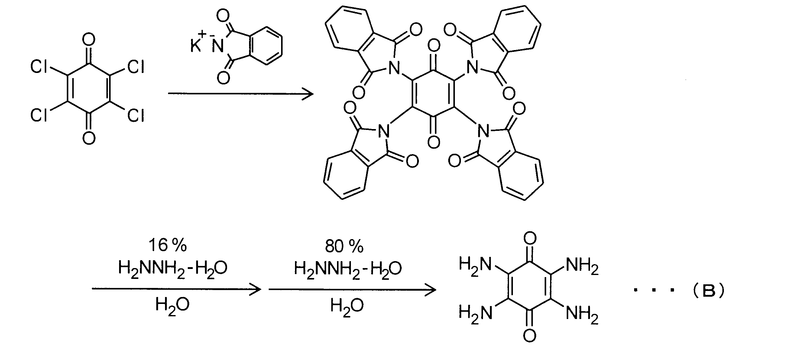
500mlのナス型フラスコにクロラニル(12.5g,50mmol)、フタル酸イミドカリウム(40.0g,216mmol)および脱水アセトニトリル(400ml)を加え、還流条件下、5時間加熱攪拌させた。反応液をろ過して固体をろ別し、この固体を水洗して反応中間体を得た。
次に300mlのナス型フラスコに16%のヒドラジン水溶液(200ml)と先の反応中間体を入れ、室温下で1時間攪拌させた。ろ過して得られた固体を水洗後、80%のヒドラジン水溶液(200ml)と混合し、70~80oCで1時間加熱攪拌した。反応液を熱時ろ過し、水、ジエチルエーテルで洗浄した後、減圧下乾燥することにより紫色固体である2,3,5,6-テトラアミノベンゾキノンを4.96g(収率:59%)得た。
次に300mlのナス型フラスコに16%のヒドラジン水溶液(200ml)と先の反応中間体を入れ、室温下で1時間攪拌させた。ろ過して得られた固体を水洗後、80%のヒドラジン水溶液(200ml)と混合し、70~80oCで1時間加熱攪拌した。反応液を熱時ろ過し、水、ジエチルエーテルで洗浄した後、減圧下乾燥することにより紫色固体である2,3,5,6-テトラアミノベンゾキノンを4.96g(収率:59%)得た。
得られた2,3,5,6-テトラアミノベンゾキノンの赤外吸収分析(IR)の測定結果を以下に示す。
IR(KBr、cm-1):549,740,826,892,975,1144,1367,1415,1556,1593,1668,2919,3164,3315,3372.
IR(KBr、cm-1):549,740,826,892,975,1144,1367,1415,1556,1593,1668,2919,3164,3315,3372.
(実施例1)
300mlのナス型フラスコにフェニルボロン酸(1.2g,10mmol)、2,3,5,6-テトラアミノベンゾキノン(504.5mg,3mmol)、トルエン(150ml)を加え、還流条件下、48時間加熱攪拌した。反応液を熱時ろ過し、得られた固体を減圧乾燥後、昇華精製することにより、下記化学式(2)で示される化合物を194mg(収率:19%)得た。
300mlのナス型フラスコにフェニルボロン酸(1.2g,10mmol)、2,3,5,6-テトラアミノベンゾキノン(504.5mg,3mmol)、トルエン(150ml)を加え、還流条件下、48時間加熱攪拌した。反応液を熱時ろ過し、得られた固体を減圧乾燥後、昇華精製することにより、下記化学式(2)で示される化合物を194mg(収率:19%)得た。

得られた化合物の質量分析、元素分析およびIR測定の結果を以下に示す。
質量分析(EI) 340 [M+].
元素分析(C18H14B2N4O2):
計算値(%) C:63.60、H:4.15、B:6.36、N:16.48、O:9.41;
実測値(%) C:61.38、H:4.16、N:15.86
IR(KBr、cm-1):569,633,691,746,992,1004,1017,1148,1247,1344,1402,1439,1505,1565,1621,3341,3464.
質量分析(EI) 340 [M+].
元素分析(C18H14B2N4O2):
計算値(%) C:63.60、H:4.15、B:6.36、N:16.48、O:9.41;
実測値(%) C:61.38、H:4.16、N:15.86
IR(KBr、cm-1):569,633,691,746,992,1004,1017,1148,1247,1344,1402,1439,1505,1565,1621,3341,3464.
(実施例2)
300mlのナス型フラスコに4-ビフェニリルボロン酸(2.0g,10mmol)、2,3,5,6-テトラアミノベンゾキノン(282mg,1.7mmol)、トルエン(150ml)を加え、還流条件下、48時間加熱攪拌した。反応液を熱時ろ過し、得られた固体を減圧乾燥後、昇華精製することにより、下記化学式(3)で示される化合物を113mg(収率:20%)得た。
300mlのナス型フラスコに4-ビフェニリルボロン酸(2.0g,10mmol)、2,3,5,6-テトラアミノベンゾキノン(282mg,1.7mmol)、トルエン(150ml)を加え、還流条件下、48時間加熱攪拌した。反応液を熱時ろ過し、得られた固体を減圧乾燥後、昇華精製することにより、下記化学式(3)で示される化合物を113mg(収率:20%)得た。

得られた化合物の質量分析および元素分析の結果を以下に示す。
質量分析(EI) 492 [M+].
元素分析(C30H22B2N4O2):
計算値(%) C:73.21、H:4.51、B:4.39、N:11.38、O:6.50;
実測値(%) C:70.56、H:4.39、N:10.79
質量分析(EI) 492 [M+].
元素分析(C30H22B2N4O2):
計算値(%) C:73.21、H:4.51、B:4.39、N:11.38、O:6.50;
実測値(%) C:70.56、H:4.39、N:10.79
(実施例3)
300mlのナス型フラスコに4-(4-トリフルオロメチル)フェニルボロン酸(2.0g,10.5mmol)、2,3,5,6-テトラアミノベンゾキノン(354mg,2.1mmol)、トルエン(150ml)を加え、還流条件下、48時間加熱攪拌した。反応液を熱時ろ過し、得られた固体を減圧乾燥後、昇華精製することにより、下記化学式(4)で示される化合物を544mg(収率:54%)得た。
300mlのナス型フラスコに4-(4-トリフルオロメチル)フェニルボロン酸(2.0g,10.5mmol)、2,3,5,6-テトラアミノベンゾキノン(354mg,2.1mmol)、トルエン(150ml)を加え、還流条件下、48時間加熱攪拌した。反応液を熱時ろ過し、得られた固体を減圧乾燥後、昇華精製することにより、下記化学式(4)で示される化合物を544mg(収率:54%)得た。

得られた化合物の質量分析および元素分析の結果を以下に示す。
質量分析(EI) 476 [M+].
元素分析(C20H12B2F6N4O2):
計算値(%) C:50.47、H:2.54、B:4.54、F:23.95、N:11.77、O:6.72;
実測値(%) C:50.01、H:2.43、N:11.61
質量分析(EI) 476 [M+].
元素分析(C20H12B2F6N4O2):
計算値(%) C:50.47、H:2.54、B:4.54、F:23.95、N:11.77、O:6.72;
実測値(%) C:50.01、H:2.43、N:11.61
(実施例4)
300mlのナス型フラスコに4-(4-トリフルオロメチルフェニル)フェニルボロン酸(380mg,1.4mmol)、2,3,5,6-テトラアミノベンゾキノン(94mg,0.56mmol)、トルエン(150ml)を加え、還流条件下、48時間加熱攪拌した。反応液を熱時ろ過し、得られた固体を減圧乾燥後、昇華精製することにより、下記化学式(5)で示される化合物を27.8mg(収率:10%)得た。
300mlのナス型フラスコに4-(4-トリフルオロメチルフェニル)フェニルボロン酸(380mg,1.4mmol)、2,3,5,6-テトラアミノベンゾキノン(94mg,0.56mmol)、トルエン(150ml)を加え、還流条件下、48時間加熱攪拌した。反応液を熱時ろ過し、得られた固体を減圧乾燥後、昇華精製することにより、下記化学式(5)で示される化合物を27.8mg(収率:10%)得た。

得られた化合物の質量分析および元素分析の結果を以下に示す。
質量分析(EI) 628 [M+].
元素分析(C32H20B2F6N4O2):
計算値(%) C:61.19、H:3.21、B:3.44、F:18.15、N:8.92、O:5.09;
実測値(%) C:60.97、H:3.05、N:8.81
質量分析(EI) 628 [M+].
元素分析(C32H20B2F6N4O2):
計算値(%) C:61.19、H:3.21、B:3.44、F:18.15、N:8.92、O:5.09;
実測値(%) C:60.97、H:3.05、N:8.81
(実施例5)
300mlのナス型フラスコに4-ヘキシルフェニルボロン酸(1.0g,4.9mmol)、2,3,5,6-テトラアミノベンゾキノン(244mg,1.45mmol)、トルエン(150ml)を加え、還流条件下、48時間加熱攪拌した。反応液を熱時ろ過し、得られた固体を減圧乾燥後、昇華精製することにより、下記化学式(6)で示される化合物を86mg(収率:12%)得た。
300mlのナス型フラスコに4-ヘキシルフェニルボロン酸(1.0g,4.9mmol)、2,3,5,6-テトラアミノベンゾキノン(244mg,1.45mmol)、トルエン(150ml)を加え、還流条件下、48時間加熱攪拌した。反応液を熱時ろ過し、得られた固体を減圧乾燥後、昇華精製することにより、下記化学式(6)で示される化合物を86mg(収率:12%)得た。

得られた化合物の1H核磁気共鳴スペクトル(1H-NMR)測定および質量分析の結果を以下に示す。
1H-NMR(CDCl3、300MHz、TMS) δ:0.86(s,8H),1.28(s,14H),1.57(s,4H),7.16(d,4H),7.91(d,4H),9.67(s,4H)
質量分析(EI) 508[M+].
1H-NMR(CDCl3、300MHz、TMS) δ:0.86(s,8H),1.28(s,14H),1.57(s,4H),7.16(d,4H),7.91(d,4H),9.67(s,4H)
質量分析(EI) 508[M+].
(実施例6 トップコンタクト型-n型有機電界効果トランジスタ)
厚さ500μmのシリコンウェハを3.5×2.5cmの大きさに切り出し、このウェハを絶縁性支持基板5とした。この基板に、オゾン処理、またはオゾン処理後にヘキサメチルジシラザン(HMDS)もしくはオクチルトリクロロシラン(OTS)の処理をした。この処理基板上に、n型シリコンウェハを形成し、これをゲート電極6とした。このゲート電極上に、熱酸化法を用いて200nmの酸化シリコン(SiO2)絶縁体層7を形成した。
次いで、SiO2上に真空蒸着法を用いて、実施例1,2,4で得られた化合物を30nm蒸着し、有機半導体層1を形成した。さらに、その有機半導体層1上に、真空蒸着法を用いて、金を50nmの厚みで蒸着し(2および3)、図1で示されるトップコンタクト型のn型有機電界効果トランジスタを得た。なお、チャネル長(L)が50、75および100μm、チャネル幅(W)が1000μmとなるようにして蒸着を行った。
厚さ500μmのシリコンウェハを3.5×2.5cmの大きさに切り出し、このウェハを絶縁性支持基板5とした。この基板に、オゾン処理、またはオゾン処理後にヘキサメチルジシラザン(HMDS)もしくはオクチルトリクロロシラン(OTS)の処理をした。この処理基板上に、n型シリコンウェハを形成し、これをゲート電極6とした。このゲート電極上に、熱酸化法を用いて200nmの酸化シリコン(SiO2)絶縁体層7を形成した。
次いで、SiO2上に真空蒸着法を用いて、実施例1,2,4で得られた化合物を30nm蒸着し、有機半導体層1を形成した。さらに、その有機半導体層1上に、真空蒸着法を用いて、金を50nmの厚みで蒸着し(2および3)、図1で示されるトップコンタクト型のn型有機電界効果トランジスタを得た。なお、チャネル長(L)が50、75および100μm、チャネル幅(W)が1000μmとなるようにして蒸着を行った。
得られたn型有機電界効果トランジスタについて、エレクトロメーターを用いて、ソース電極およびドレイン電極間に10~60Vの電圧を印加し、ゲート電圧を-20~100Vの範囲で変化させて、電圧-電流曲線を25℃の温度において求め、そのトランジスタ特性を評価した。トランジスタ特性は、正バイアスについてのみ観察された。このことは、得られた電界効果トランジスタがn型有機電界効果トランジスタであることを意味する。
電界効果移動度(μ)は、ドレイン電流Idを表わす下記式(C)を用いて算出した。
Id=(W/2L)・μ・Ci・(Vg-Vt)2・・・(C)
前記式(C)において、Lはゲート長であり、Wはゲート幅である。また、Ciは絶縁層の単位面積当たりの容量であり、Vgはゲート電圧であり、Vtは閾値電圧である。
Id=(W/2L)・μ・Ci・(Vg-Vt)2・・・(C)
前記式(C)において、Lはゲート長であり、Wはゲート幅である。また、Ciは絶縁層の単位面積当たりの容量であり、Vgはゲート電圧であり、Vtは閾値電圧である。
また、オン/オフ比は、最大および最小ドレイン電流値(Id)の比より算出した。得られたトランジスタ特性評価の結果を表1に示す。
(実施例7 ボトムコンタクト型-n型有機電界効果トランジスタ)
実施例6と同様に形成した酸化シリコン絶縁体層7(膜厚300nm)上にフォトリソグラフィー法を用いて櫛形パターンの電極(2および3)を形成した。電極の層構造は、酸化シリコン上にクロム(Cr)を膜厚10nmまで蒸着し、その上に金を膜厚20nmまで蒸着した。また、櫛形パターンは、電極のチャネル長が25μm、チャネル幅が294μm(6μm×49)となるようにした。
この電極(2および3)を形成した酸化シリコン絶縁体層7に圧力10-5Paの超真空下で基板温度を室温または50℃、蒸着速度0.1~0.3Åで実施例2~5で得られた化合物を50nm蒸着して有機半導体層1を形成し、図2で示されるボトムコンタクト型のn型有機電界効果トランジスタを得た。また、塗布法の場合はクロロホルム溶液を基板にドロップキャストして製膜した。
実施例6と同様に形成した酸化シリコン絶縁体層7(膜厚300nm)上にフォトリソグラフィー法を用いて櫛形パターンの電極(2および3)を形成した。電極の層構造は、酸化シリコン上にクロム(Cr)を膜厚10nmまで蒸着し、その上に金を膜厚20nmまで蒸着した。また、櫛形パターンは、電極のチャネル長が25μm、チャネル幅が294μm(6μm×49)となるようにした。
この電極(2および3)を形成した酸化シリコン絶縁体層7に圧力10-5Paの超真空下で基板温度を室温または50℃、蒸着速度0.1~0.3Åで実施例2~5で得られた化合物を50nm蒸着して有機半導体層1を形成し、図2で示されるボトムコンタクト型のn型有機電界効果トランジスタを得た。また、塗布法の場合はクロロホルム溶液を基板にドロップキャストして製膜した。
得られたn型有機電界効果トランジスタについて、実施例6と同様にトランジスタ特性を評価した。トランジスタ特性評価の結果を表1に示す。
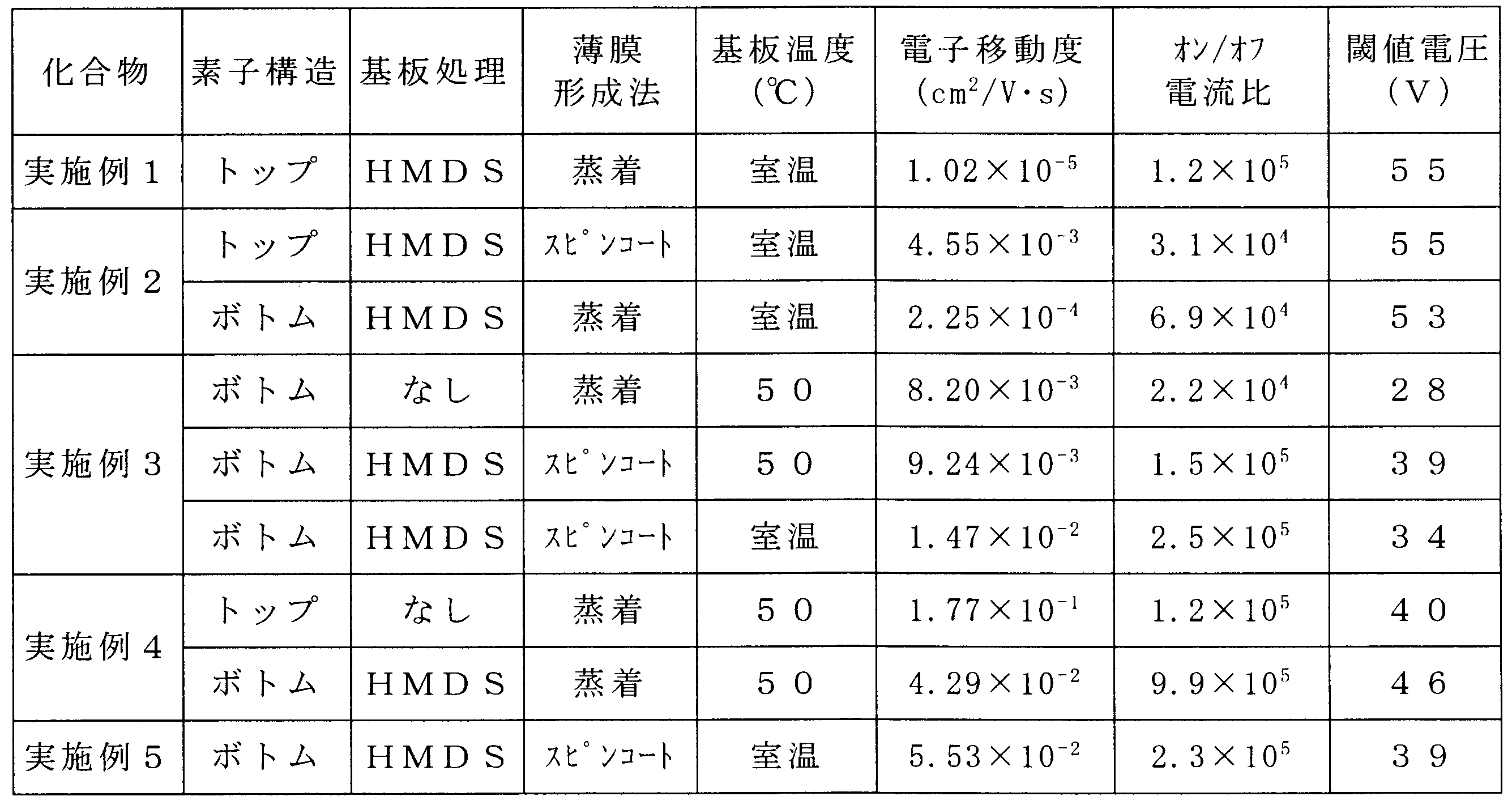
表1において、素子構造の表記である、トップとはトップコンタクト型、ボトムとはボトムコンタクト型を示し、基板処理の表記である、HMDSとはヘキサメチルジシラザンで処理をしたことを示す。
本発明のジアザボロール化合物は、有機電界効果トランジスタの有機半導体材料として用いられる。
Claims (5)
- 下記化学式(1)

- 前記置換基が、直鎖、分岐または環状アルキル基の水素原子のうち80~100%がフッ素原子で置換された炭素数1~20のパーフルオロアルキル基であることを特徴とする請求項1に記載のジアザボロール化合物。
- 下記化学式(1)

- 前記置換基が、直鎖、分岐または環状アルキル基の水素原子のうち80~100%がフッ素原子で置換された炭素数1~20のパーフルオロアルキル基であることを特徴とする請求項3に記載の有機半導体材料。
- 基板上で、ソース電極およびドレイン電極の間の電流路を形成している有機半導体層と、前記電流路の電流を制御しているゲート電極とが、絶縁体層で隔離されており、前記有機半導体層に、下記化学式(1)
Priority Applications (1)
| Application Number | Priority Date | Filing Date | Title |
|---|---|---|---|
| JP2011514935A JP5637985B2 (ja) | 2009-12-08 | 2010-12-06 | ジアザボロール化合物、およびそれを含有した電界効果トランジスタ |
Applications Claiming Priority (2)
| Application Number | Priority Date | Filing Date | Title |
|---|---|---|---|
| JP2009-278733 | 2009-12-08 | ||
| JP2009278733 | 2009-12-08 |
Publications (1)
| Publication Number | Publication Date |
|---|---|
| WO2011071017A1 true WO2011071017A1 (ja) | 2011-06-16 |
Family
ID=44145562
Family Applications (1)
| Application Number | Title | Priority Date | Filing Date |
|---|---|---|---|
| PCT/JP2010/071828 Ceased WO2011071017A1 (ja) | 2009-12-08 | 2010-12-06 | ジアザボロール化合物、およびそれを含有した電界効果トランジスタ |
Country Status (2)
| Country | Link |
|---|---|
| JP (1) | JP5637985B2 (ja) |
| WO (1) | WO2011071017A1 (ja) |
Cited By (2)
| Publication number | Priority date | Publication date | Assignee | Title |
|---|---|---|---|---|
| JP2013152969A (ja) * | 2012-01-24 | 2013-08-08 | Hitachi Ltd | グラフェントランジスタ |
| CN116425645A (zh) * | 2023-01-10 | 2023-07-14 | 浙江理工大学嵊州创新研究院有限公司 | 一种2,3,5,6-四氨基苯醌的制备方法及应用 |
-
2010
- 2010-12-06 JP JP2011514935A patent/JP5637985B2/ja not_active Expired - Fee Related
- 2010-12-06 WO PCT/JP2010/071828 patent/WO2011071017A1/ja not_active Ceased
Non-Patent Citations (1)
| Title |
|---|
| KOJIMA, T. ET AL.: "Development of Organic Electronic Devices Using Boronate Esters and Related Heterocycles", CHEMISTRY LETTERS, vol. 37, no. 11, 2008, pages 1122 - 1123 * |
Cited By (2)
| Publication number | Priority date | Publication date | Assignee | Title |
|---|---|---|---|---|
| JP2013152969A (ja) * | 2012-01-24 | 2013-08-08 | Hitachi Ltd | グラフェントランジスタ |
| CN116425645A (zh) * | 2023-01-10 | 2023-07-14 | 浙江理工大学嵊州创新研究院有限公司 | 一种2,3,5,6-四氨基苯醌的制备方法及应用 |
Also Published As
| Publication number | Publication date |
|---|---|
| JPWO2011071017A1 (ja) | 2013-04-22 |
| JP5637985B2 (ja) | 2014-12-10 |
Similar Documents
| Publication | Publication Date | Title |
|---|---|---|
| JP5454139B2 (ja) | カーボンナノチューブ複合体、有機半導体コンポジットならびに電界効果型トランジスタ | |
| CN105102462B (zh) | 含有氧族元素的有机化合物、其制造方法以及用途 | |
| CN103958520B (zh) | 具有半导体特性的化合物及相关组合物和装置 | |
| CN104125951B (zh) | 含硫族元素有机化合物与其制造方法、有机半导体材料、有机半导体膜及有机场效应晶体管 | |
| CN102574868B (zh) | 取代苯并硫属并苯化合物、包含该化合物的薄膜以及包括该薄膜的有机半导体装置 | |
| JP6080870B2 (ja) | 溶液プロセス用有機半導体材料及び有機半導体デバイス | |
| JP6170488B2 (ja) | 新規縮合多環芳香族化合物及びその用途 | |
| JP6332644B2 (ja) | 化合物、高分子化合物、有機半導体材料、有機半導体デバイス、化合物の合成方法、高分子化合物の合成方法 | |
| WO2008032715A1 (en) | Organic semiconductor material, organic semiconductor device using the same, and their production methods | |
| JP5344441B2 (ja) | 新規化合物及びその製造方法、並びに有機半導体材料及び有機半導体デバイス | |
| JP5897050B2 (ja) | 有機薄膜トランジスタ、有機半導体薄膜および有機半導体材料 | |
| CN101421862A (zh) | 作为有机半导体的醌型体系 | |
| JP5650107B2 (ja) | チエノピラジン化合物、およびそれを含有した電界効果トランジスタ | |
| JP5637985B2 (ja) | ジアザボロール化合物、およびそれを含有した電界効果トランジスタ | |
| JP5228411B2 (ja) | [1]ベンゾカルコゲノ[3,2−b][1]ベンゾカルコゲノフェン骨格を有する化合物およびこれを用いた有機トランジスタ | |
| JP6678515B2 (ja) | 化合物、組成物、および有機半導体デバイス | |
| WO2021054161A1 (ja) | 縮合多環芳香族化合物 | |
| JP2015141912A (ja) | 有機薄膜トランジスタ、有機半導体薄膜および有機半導体材料 | |
| JP7317301B2 (ja) | 有機半導体化合物及びその用途 | |
| JPWO2008108442A1 (ja) | 新規ポルフィラジン誘導体およびその中間体、新規ポルフィラジン誘導体およびその中間体の製造方法、並びにその利用 | |
| JP2017171607A (ja) | 化合物、組成物、有機半導体デバイス、および化合物を製造する方法 | |
| JP6184234B2 (ja) | 有機薄膜トランジスタ、有機半導体薄膜および有機半導体材料 |
Legal Events
| Date | Code | Title | Description |
|---|---|---|---|
| WWE | Wipo information: entry into national phase |
Ref document number: 2011514935 Country of ref document: JP |
|
| 121 | Ep: the epo has been informed by wipo that ep was designated in this application |
Ref document number: 10835937 Country of ref document: EP Kind code of ref document: A1 |
|
| NENP | Non-entry into the national phase |
Ref country code: DE |
|
| 122 | Ep: pct application non-entry in european phase |
Ref document number: 10835937 Country of ref document: EP Kind code of ref document: A1 |