WO2011052509A1 - Method for production of organic photoelectric conversion element - Google Patents
Method for production of organic photoelectric conversion element Download PDFInfo
- Publication number
- WO2011052509A1 WO2011052509A1 PCT/JP2010/068732 JP2010068732W WO2011052509A1 WO 2011052509 A1 WO2011052509 A1 WO 2011052509A1 JP 2010068732 W JP2010068732 W JP 2010068732W WO 2011052509 A1 WO2011052509 A1 WO 2011052509A1
- Authority
- WO
- WIPO (PCT)
- Prior art keywords
- substrate
- layer
- photoelectric conversion
- conversion element
- organic photoelectric
- Prior art date
Links
- 238000006243 chemical reaction Methods 0.000 title claims abstract description 93
- 238000004519 manufacturing process Methods 0.000 title claims abstract description 75
- 239000000758 substrate Substances 0.000 claims abstract description 142
- 238000000034 method Methods 0.000 claims abstract description 48
- 239000002904 solvent Substances 0.000 claims description 18
- 238000005304 joining Methods 0.000 claims description 17
- 229910052751 metal Inorganic materials 0.000 claims description 9
- 239000002184 metal Substances 0.000 claims description 9
- 150000002894 organic compounds Chemical class 0.000 claims description 8
- 150000002484 inorganic compounds Chemical class 0.000 claims description 7
- 229910010272 inorganic material Inorganic materials 0.000 claims description 7
- 229910045601 alloy Inorganic materials 0.000 claims description 6
- 239000000956 alloy Substances 0.000 claims description 6
- LFQSCWFLJHTTHZ-UHFFFAOYSA-N Ethanol Chemical compound CCO LFQSCWFLJHTTHZ-UHFFFAOYSA-N 0.000 claims description 5
- 238000003825 pressing Methods 0.000 claims description 4
- 150000004945 aromatic hydrocarbons Chemical class 0.000 claims description 3
- 230000004888 barrier function Effects 0.000 claims description 3
- XLYOFNOQVPJJNP-UHFFFAOYSA-N water Chemical compound O XLYOFNOQVPJJNP-UHFFFAOYSA-N 0.000 claims description 3
- 150000001338 aliphatic hydrocarbons Chemical class 0.000 claims description 2
- 238000012545 processing Methods 0.000 claims description 2
- 239000010410 layer Substances 0.000 abstract description 229
- 239000012044 organic layer Substances 0.000 abstract description 8
- 230000006866 deterioration Effects 0.000 abstract description 3
- 150000001875 compounds Chemical class 0.000 description 30
- 239000000463 material Substances 0.000 description 27
- XMWRBQBLMFGWIX-UHFFFAOYSA-N C60 fullerene Chemical class C12=C3C(C4=C56)=C7C8=C5C5=C9C%10=C6C6=C4C1=C1C4=C6C6=C%10C%10=C9C9=C%11C5=C8C5=C8C7=C3C3=C7C2=C1C1=C2C4=C6C4=C%10C6=C9C9=C%11C5=C5C8=C3C3=C7C1=C1C2=C4C6=C2C9=C5C3=C12 XMWRBQBLMFGWIX-UHFFFAOYSA-N 0.000 description 22
- 239000010408 film Substances 0.000 description 21
- 239000010409 thin film Substances 0.000 description 15
- 229910003472 fullerene Inorganic materials 0.000 description 12
- 230000005525 hole transport Effects 0.000 description 11
- 239000004020 conductor Substances 0.000 description 10
- MCEWYIDBDVPMES-UHFFFAOYSA-N [60]pcbm Chemical compound C123C(C4=C5C6=C7C8=C9C%10=C%11C%12=C%13C%14=C%15C%16=C%17C%18=C(C=%19C=%20C%18=C%18C%16=C%13C%13=C%11C9=C9C7=C(C=%20C9=C%13%18)C(C7=%19)=C96)C6=C%11C%17=C%15C%13=C%15C%14=C%12C%12=C%10C%10=C85)=C9C7=C6C2=C%11C%13=C2C%15=C%12C%10=C4C23C1(CCCC(=O)OC)C1=CC=CC=C1 MCEWYIDBDVPMES-UHFFFAOYSA-N 0.000 description 9
- 238000000576 coating method Methods 0.000 description 9
- 239000011521 glass Substances 0.000 description 9
- -1 polyethylene terephthalate Polymers 0.000 description 8
- 239000011248 coating agent Substances 0.000 description 7
- 239000004065 semiconductor Substances 0.000 description 7
- HEDRZPFGACZZDS-UHFFFAOYSA-N Chloroform Chemical compound ClC(Cl)Cl HEDRZPFGACZZDS-UHFFFAOYSA-N 0.000 description 6
- YXFVVABEGXRONW-UHFFFAOYSA-N Toluene Chemical compound CC1=CC=CC=C1 YXFVVABEGXRONW-UHFFFAOYSA-N 0.000 description 6
- 239000010931 gold Substances 0.000 description 6
- OKTJSMMVPCPJKN-UHFFFAOYSA-N Carbon Chemical compound [C] OKTJSMMVPCPJKN-UHFFFAOYSA-N 0.000 description 5
- UUIQMZJEGPQKFD-UHFFFAOYSA-N Methyl butyrate Chemical compound CCCC(=O)OC UUIQMZJEGPQKFD-UHFFFAOYSA-N 0.000 description 5
- 229910010413 TiO 2 Inorganic materials 0.000 description 5
- PCHJSUWPFVWCPO-UHFFFAOYSA-N gold Chemical compound [Au] PCHJSUWPFVWCPO-UHFFFAOYSA-N 0.000 description 5
- 229910052737 gold Inorganic materials 0.000 description 5
- 229920000301 poly(3-hexylthiophene-2,5-diyl) polymer Polymers 0.000 description 5
- 238000004528 spin coating Methods 0.000 description 5
- CSCPPACGZOOCGX-UHFFFAOYSA-N Acetone Chemical compound CC(C)=O CSCPPACGZOOCGX-UHFFFAOYSA-N 0.000 description 4
- CBENFWSGALASAD-UHFFFAOYSA-N Ozone Chemical compound [O-][O+]=O CBENFWSGALASAD-UHFFFAOYSA-N 0.000 description 4
- 229920001609 Poly(3,4-ethylenedioxythiophene) Polymers 0.000 description 4
- GWEVSGVZZGPLCZ-UHFFFAOYSA-N Titan oxide Chemical compound O=[Ti]=O GWEVSGVZZGPLCZ-UHFFFAOYSA-N 0.000 description 4
- MVPPADPHJFYWMZ-UHFFFAOYSA-N chlorobenzene Chemical compound ClC1=CC=CC=C1 MVPPADPHJFYWMZ-UHFFFAOYSA-N 0.000 description 4
- 238000010438 heat treatment Methods 0.000 description 4
- BASFCYQUMIYNBI-UHFFFAOYSA-N platinum Chemical compound [Pt] BASFCYQUMIYNBI-UHFFFAOYSA-N 0.000 description 4
- 238000007639 printing Methods 0.000 description 4
- OGIDPMRJRNCKJF-UHFFFAOYSA-N titanium oxide Inorganic materials [Ti]=O OGIDPMRJRNCKJF-UHFFFAOYSA-N 0.000 description 4
- 229910000838 Al alloy Inorganic materials 0.000 description 3
- RYGMFSIKBFXOCR-UHFFFAOYSA-N Copper Chemical compound [Cu] RYGMFSIKBFXOCR-UHFFFAOYSA-N 0.000 description 3
- YMWUJEATGCHHMB-UHFFFAOYSA-N Dichloromethane Chemical compound ClCCl YMWUJEATGCHHMB-UHFFFAOYSA-N 0.000 description 3
- KFZMGEQAYNKOFK-UHFFFAOYSA-N Isopropanol Chemical compound CC(C)O KFZMGEQAYNKOFK-UHFFFAOYSA-N 0.000 description 3
- OKKJLVBELUTLKV-UHFFFAOYSA-N Methanol Chemical compound OC OKKJLVBELUTLKV-UHFFFAOYSA-N 0.000 description 3
- BQCADISMDOOEFD-UHFFFAOYSA-N Silver Chemical compound [Ag] BQCADISMDOOEFD-UHFFFAOYSA-N 0.000 description 3
- 229910052802 copper Inorganic materials 0.000 description 3
- 239000010949 copper Substances 0.000 description 3
- 238000001035 drying Methods 0.000 description 3
- 239000007772 electrode material Substances 0.000 description 3
- 125000005842 heteroatom Chemical group 0.000 description 3
- 239000000203 mixture Substances 0.000 description 3
- 229920000767 polyaniline Polymers 0.000 description 3
- 229920000123 polythiophene Polymers 0.000 description 3
- 229910052709 silver Inorganic materials 0.000 description 3
- 239000004332 silver Substances 0.000 description 3
- CXWXQJXEFPUFDZ-UHFFFAOYSA-N tetralin Chemical compound C1=CC=C2CCCCC2=C1 CXWXQJXEFPUFDZ-UHFFFAOYSA-N 0.000 description 3
- RFFLAFLAYFXFSW-UHFFFAOYSA-N 1,2-dichlorobenzene Chemical compound ClC1=CC=CC=C1Cl RFFLAFLAYFXFSW-UHFFFAOYSA-N 0.000 description 2
- STTGYIUESPWXOW-UHFFFAOYSA-N 2,9-dimethyl-4,7-diphenyl-1,10-phenanthroline Chemical compound C=12C=CC3=C(C=4C=CC=CC=4)C=C(C)N=C3C2=NC(C)=CC=1C1=CC=CC=C1 STTGYIUESPWXOW-UHFFFAOYSA-N 0.000 description 2
- 229910001316 Ag alloy Inorganic materials 0.000 description 2
- IJGRMHOSHXDMSA-UHFFFAOYSA-N Atomic nitrogen Chemical compound N#N IJGRMHOSHXDMSA-UHFFFAOYSA-N 0.000 description 2
- 229910000846 In alloy Inorganic materials 0.000 description 2
- PXHVJJICTQNCMI-UHFFFAOYSA-N Nickel Chemical compound [Ni] PXHVJJICTQNCMI-UHFFFAOYSA-N 0.000 description 2
- CTQNGGLPUBDAKN-UHFFFAOYSA-N O-Xylene Chemical compound CC1=CC=CC=C1C CTQNGGLPUBDAKN-UHFFFAOYSA-N 0.000 description 2
- 229920000144 PEDOT:PSS Polymers 0.000 description 2
- WYURNTSHIVDZCO-UHFFFAOYSA-N Tetrahydrofuran Chemical compound C1CCOC1 WYURNTSHIVDZCO-UHFFFAOYSA-N 0.000 description 2
- RTAQQCXQSZGOHL-UHFFFAOYSA-N Titanium Chemical compound [Ti] RTAQQCXQSZGOHL-UHFFFAOYSA-N 0.000 description 2
- XLOMVQKBTHCTTD-UHFFFAOYSA-N Zinc monoxide Chemical compound [Zn]=O XLOMVQKBTHCTTD-UHFFFAOYSA-N 0.000 description 2
- 229910052783 alkali metal Inorganic materials 0.000 description 2
- 150000001340 alkali metals Chemical class 0.000 description 2
- 229910052784 alkaline earth metal Inorganic materials 0.000 description 2
- 150000001342 alkaline earth metals Chemical class 0.000 description 2
- 229910052782 aluminium Inorganic materials 0.000 description 2
- XAGFODPZIPBFFR-UHFFFAOYSA-N aluminium Chemical compound [Al] XAGFODPZIPBFFR-UHFFFAOYSA-N 0.000 description 2
- 150000004982 aromatic amines Chemical class 0.000 description 2
- 230000015572 biosynthetic process Effects 0.000 description 2
- OCKPCBLVNKHBMX-UHFFFAOYSA-N butylbenzene Chemical compound CCCCC1=CC=CC=C1 OCKPCBLVNKHBMX-UHFFFAOYSA-N 0.000 description 2
- 239000002041 carbon nanotube Substances 0.000 description 2
- 229910021393 carbon nanotube Inorganic materials 0.000 description 2
- 238000004140 cleaning Methods 0.000 description 2
- NNBZCPXTIHJBJL-UHFFFAOYSA-N decalin Chemical compound C1CCCC2CCCCC21 NNBZCPXTIHJBJL-UHFFFAOYSA-N 0.000 description 2
- 229910001873 dinitrogen Inorganic materials 0.000 description 2
- 238000005530 etching Methods 0.000 description 2
- 229910002804 graphite Inorganic materials 0.000 description 2
- 239000010439 graphite Substances 0.000 description 2
- 238000007756 gravure coating Methods 0.000 description 2
- 238000007646 gravure printing Methods 0.000 description 2
- AMGQUBHHOARCQH-UHFFFAOYSA-N indium;oxotin Chemical compound [In].[Sn]=O AMGQUBHHOARCQH-UHFFFAOYSA-N 0.000 description 2
- 238000007641 inkjet printing Methods 0.000 description 2
- PQXKHYXIUOZZFA-UHFFFAOYSA-M lithium fluoride Chemical compound [Li+].[F-] PQXKHYXIUOZZFA-UHFFFAOYSA-M 0.000 description 2
- QSHDDOUJBYECFT-UHFFFAOYSA-N mercury Chemical compound [Hg] QSHDDOUJBYECFT-UHFFFAOYSA-N 0.000 description 2
- 229910052753 mercury Inorganic materials 0.000 description 2
- 229910044991 metal oxide Inorganic materials 0.000 description 2
- 150000004706 metal oxides Chemical class 0.000 description 2
- 150000002739 metals Chemical class 0.000 description 2
- 238000000059 patterning Methods 0.000 description 2
- 238000000206 photolithography Methods 0.000 description 2
- 229910052697 platinum Inorganic materials 0.000 description 2
- 238000010248 power generation Methods 0.000 description 2
- 238000007650 screen-printing Methods 0.000 description 2
- 238000004544 sputter deposition Methods 0.000 description 2
- YTZKOQUCBOVLHL-UHFFFAOYSA-N tert-butylbenzene Chemical compound CC(C)(C)C1=CC=CC=C1 YTZKOQUCBOVLHL-UHFFFAOYSA-N 0.000 description 2
- VZGDMQKNWNREIO-UHFFFAOYSA-N tetrachloromethane Chemical compound ClC(Cl)(Cl)Cl VZGDMQKNWNREIO-UHFFFAOYSA-N 0.000 description 2
- XOLBLPGZBRYERU-UHFFFAOYSA-N tin dioxide Chemical compound O=[Sn]=O XOLBLPGZBRYERU-UHFFFAOYSA-N 0.000 description 2
- 229910001887 tin oxide Inorganic materials 0.000 description 2
- 239000010936 titanium Substances 0.000 description 2
- 229910052719 titanium Inorganic materials 0.000 description 2
- 229930195735 unsaturated hydrocarbon Natural products 0.000 description 2
- 238000007740 vapor deposition Methods 0.000 description 2
- 239000008096 xylene Substances 0.000 description 2
- SCYULBFZEHDVBN-UHFFFAOYSA-N 1,1-Dichloroethane Chemical compound CC(Cl)Cl SCYULBFZEHDVBN-UHFFFAOYSA-N 0.000 description 1
- RELMFMZEBKVZJC-UHFFFAOYSA-N 1,2,3-trichlorobenzene Chemical compound ClC1=CC=CC(Cl)=C1Cl RELMFMZEBKVZJC-UHFFFAOYSA-N 0.000 description 1
- AZQWKYJCGOJGHM-UHFFFAOYSA-N 1,4-benzoquinone Chemical compound O=C1C=CC(=O)C=C1 AZQWKYJCGOJGHM-UHFFFAOYSA-N 0.000 description 1
- OCJBOOLMMGQPQU-UHFFFAOYSA-N 1,4-dichlorobenzene Chemical compound ClC1=CC=C(Cl)C=C1 OCJBOOLMMGQPQU-UHFFFAOYSA-N 0.000 description 1
- MPPPKRYCTPRNTB-UHFFFAOYSA-N 1-bromobutane Chemical compound CCCCBr MPPPKRYCTPRNTB-UHFFFAOYSA-N 0.000 description 1
- MNDIARAMWBIKFW-UHFFFAOYSA-N 1-bromohexane Chemical compound CCCCCCBr MNDIARAMWBIKFW-UHFFFAOYSA-N 0.000 description 1
- YZWKKMVJZFACSU-UHFFFAOYSA-N 1-bromopentane Chemical compound CCCCCBr YZWKKMVJZFACSU-UHFFFAOYSA-N 0.000 description 1
- VFWCMGCRMGJXDK-UHFFFAOYSA-N 1-chlorobutane Chemical compound CCCCCl VFWCMGCRMGJXDK-UHFFFAOYSA-N 0.000 description 1
- MLRVZFYXUZQSRU-UHFFFAOYSA-N 1-chlorohexane Chemical compound CCCCCCCl MLRVZFYXUZQSRU-UHFFFAOYSA-N 0.000 description 1
- SQCZQTSHSZLZIQ-UHFFFAOYSA-N 1-chloropentane Chemical compound CCCCCCl SQCZQTSHSZLZIQ-UHFFFAOYSA-N 0.000 description 1
- GKWLILHTTGWKLQ-UHFFFAOYSA-N 2,3-dihydrothieno[3,4-b][1,4]dioxine Chemical compound O1CCOC2=CSC=C21 GKWLILHTTGWKLQ-UHFFFAOYSA-N 0.000 description 1
- VFBJMPNFKOMEEW-UHFFFAOYSA-N 2,3-diphenylbut-2-enedinitrile Chemical group C=1C=CC=CC=1C(C#N)=C(C#N)C1=CC=CC=C1 VFBJMPNFKOMEEW-UHFFFAOYSA-N 0.000 description 1
- CMSGUKVDXXTJDQ-UHFFFAOYSA-N 4-(2-naphthalen-1-ylethylamino)-4-oxobutanoic acid Chemical compound C1=CC=C2C(CCNC(=O)CCC(=O)O)=CC=CC2=C1 CMSGUKVDXXTJDQ-UHFFFAOYSA-N 0.000 description 1
- DDTHMESPCBONDT-UHFFFAOYSA-N 4-(4-oxocyclohexa-2,5-dien-1-ylidene)cyclohexa-2,5-dien-1-one Chemical class C1=CC(=O)C=CC1=C1C=CC(=O)C=C1 DDTHMESPCBONDT-UHFFFAOYSA-N 0.000 description 1
- 239000005725 8-Hydroxyquinoline Chemical class 0.000 description 1
- AZSFNTBGCTUQFX-UHFFFAOYSA-N C12=C3C(C4=C5C=6C7=C8C9=C(C%10=6)C6=C%11C=%12C%13=C%14C%11=C9C9=C8C8=C%11C%15=C%16C=%17C(C=%18C%19=C4C7=C8C%15=%18)=C4C7=C8C%15=C%18C%20=C(C=%178)C%16=C8C%11=C9C%14=C8C%20=C%13C%18=C8C9=%12)=C%19C4=C2C7=C2C%15=C8C=4C2=C1C12C3=C5C%10=C3C6=C9C=4C32C1(CCCC(=O)OC)C1=CC=CC=C1 Chemical compound C12=C3C(C4=C5C=6C7=C8C9=C(C%10=6)C6=C%11C=%12C%13=C%14C%11=C9C9=C8C8=C%11C%15=C%16C=%17C(C=%18C%19=C4C7=C8C%15=%18)=C4C7=C8C%15=C%18C%20=C(C=%178)C%16=C8C%11=C9C%14=C8C%20=C%13C%18=C8C9=%12)=C%19C4=C2C7=C2C%15=C8C=4C2=C1C12C3=C5C%10=C3C6=C9C=4C32C1(CCCC(=O)OC)C1=CC=CC=C1 AZSFNTBGCTUQFX-UHFFFAOYSA-N 0.000 description 1
- OYPRJOBELJOOCE-UHFFFAOYSA-N Calcium Chemical compound [Ca] OYPRJOBELJOOCE-UHFFFAOYSA-N 0.000 description 1
- 229910052684 Cerium Inorganic materials 0.000 description 1
- 229910052693 Europium Inorganic materials 0.000 description 1
- DGAQECJNVWCQMB-PUAWFVPOSA-M Ilexoside XXIX Chemical compound C[C@@H]1CC[C@@]2(CC[C@@]3(C(=CC[C@H]4[C@]3(CC[C@@H]5[C@@]4(CC[C@@H](C5(C)C)OS(=O)(=O)[O-])C)C)[C@@H]2[C@]1(C)O)C)C(=O)O[C@H]6[C@@H]([C@H]([C@@H]([C@H](O6)CO)O)O)O.[Na+] DGAQECJNVWCQMB-PUAWFVPOSA-M 0.000 description 1
- WHXSMMKQMYFTQS-UHFFFAOYSA-N Lithium Chemical compound [Li] WHXSMMKQMYFTQS-UHFFFAOYSA-N 0.000 description 1
- FYYHWMGAXLPEAU-UHFFFAOYSA-N Magnesium Chemical compound [Mg] FYYHWMGAXLPEAU-UHFFFAOYSA-N 0.000 description 1
- 229910000861 Mg alloy Inorganic materials 0.000 description 1
- 229930192627 Naphthoquinone Natural products 0.000 description 1
- 239000004642 Polyimide Substances 0.000 description 1
- 229920000292 Polyquinoline Polymers 0.000 description 1
- ZLMJMSJWJFRBEC-UHFFFAOYSA-N Potassium Chemical compound [K] ZLMJMSJWJFRBEC-UHFFFAOYSA-N 0.000 description 1
- 101100012902 Saccharomyces cerevisiae (strain ATCC 204508 / S288c) FIG2 gene Proteins 0.000 description 1
- 101100233916 Saccharomyces cerevisiae (strain ATCC 204508 / S288c) KAR5 gene Proteins 0.000 description 1
- 229910052772 Samarium Inorganic materials 0.000 description 1
- 229910052581 Si3N4 Inorganic materials 0.000 description 1
- VYPSYNLAJGMNEJ-UHFFFAOYSA-N Silicium dioxide Chemical compound O=[Si]=O VYPSYNLAJGMNEJ-UHFFFAOYSA-N 0.000 description 1
- 229910052771 Terbium Inorganic materials 0.000 description 1
- DHXVGJBLRPWPCS-UHFFFAOYSA-N Tetrahydropyran Chemical compound C1CCOCC1 DHXVGJBLRPWPCS-UHFFFAOYSA-N 0.000 description 1
- ATJFFYVFTNAWJD-UHFFFAOYSA-N Tin Chemical compound [Sn] ATJFFYVFTNAWJD-UHFFFAOYSA-N 0.000 description 1
- 229910052769 Ytterbium Inorganic materials 0.000 description 1
- HCHKCACWOHOZIP-UHFFFAOYSA-N Zinc Chemical compound [Zn] HCHKCACWOHOZIP-UHFFFAOYSA-N 0.000 description 1
- ULGYAEQHFNJYML-UHFFFAOYSA-N [AlH3].[Ca] Chemical compound [AlH3].[Ca] ULGYAEQHFNJYML-UHFFFAOYSA-N 0.000 description 1
- JFBZPFYRPYOZCQ-UHFFFAOYSA-N [Li].[Al] Chemical compound [Li].[Al] JFBZPFYRPYOZCQ-UHFFFAOYSA-N 0.000 description 1
- JHYLKGDXMUDNEO-UHFFFAOYSA-N [Mg].[In] Chemical compound [Mg].[In] JHYLKGDXMUDNEO-UHFFFAOYSA-N 0.000 description 1
- 150000001298 alcohols Chemical class 0.000 description 1
- SNAAJJQQZSMGQD-UHFFFAOYSA-N aluminum magnesium Chemical compound [Mg].[Al] SNAAJJQQZSMGQD-UHFFFAOYSA-N 0.000 description 1
- PYKYMHQGRFAEBM-UHFFFAOYSA-N anthraquinone Natural products CCC(=O)c1c(O)c2C(=O)C3C(C=CC=C3O)C(=O)c2cc1CC(=O)OC PYKYMHQGRFAEBM-UHFFFAOYSA-N 0.000 description 1
- 150000004056 anthraquinones Chemical class 0.000 description 1
- QVGXLLKOCUKJST-UHFFFAOYSA-N atomic oxygen Chemical compound [O] QVGXLLKOCUKJST-UHFFFAOYSA-N 0.000 description 1
- 229910052788 barium Inorganic materials 0.000 description 1
- DSAJWYNOEDNPEQ-UHFFFAOYSA-N barium atom Chemical compound [Ba] DSAJWYNOEDNPEQ-UHFFFAOYSA-N 0.000 description 1
- AQNQQHJNRPDOQV-UHFFFAOYSA-N bromocyclohexane Chemical compound BrC1CCCCC1 AQNQQHJNRPDOQV-UHFFFAOYSA-N 0.000 description 1
- 229910052792 caesium Inorganic materials 0.000 description 1
- TVFDJXOCXUVLDH-UHFFFAOYSA-N caesium atom Chemical compound [Cs] TVFDJXOCXUVLDH-UHFFFAOYSA-N 0.000 description 1
- 229910052791 calcium Inorganic materials 0.000 description 1
- 239000011575 calcium Substances 0.000 description 1
- 229910052799 carbon Inorganic materials 0.000 description 1
- 238000005266 casting Methods 0.000 description 1
- 239000003054 catalyst Substances 0.000 description 1
- ZMIGMASIKSOYAM-UHFFFAOYSA-N cerium Chemical compound [Ce][Ce][Ce][Ce][Ce][Ce][Ce][Ce][Ce][Ce][Ce][Ce][Ce][Ce][Ce][Ce][Ce][Ce][Ce][Ce][Ce][Ce][Ce][Ce][Ce][Ce][Ce][Ce][Ce][Ce][Ce][Ce][Ce][Ce][Ce][Ce][Ce][Ce] ZMIGMASIKSOYAM-UHFFFAOYSA-N 0.000 description 1
- 229910017052 cobalt Inorganic materials 0.000 description 1
- 239000010941 cobalt Substances 0.000 description 1
- GUTLYIVDDKVIGB-UHFFFAOYSA-N cobalt atom Chemical compound [Co] GUTLYIVDDKVIGB-UHFFFAOYSA-N 0.000 description 1
- 239000002131 composite material Substances 0.000 description 1
- 229920001940 conductive polymer Polymers 0.000 description 1
- 239000000470 constituent Substances 0.000 description 1
- 239000004148 curcumin Substances 0.000 description 1
- WVIIMZNLDWSIRH-UHFFFAOYSA-N cyclohexylcyclohexane Chemical group C1CCCCC1C1CCCCC1 WVIIMZNLDWSIRH-UHFFFAOYSA-N 0.000 description 1
- 229940117389 dichlorobenzene Drugs 0.000 description 1
- 238000003618 dip coating Methods 0.000 description 1
- 238000004090 dissolution Methods 0.000 description 1
- 125000005678 ethenylene group Chemical group [H]C([*:1])=C([H])[*:2] 0.000 description 1
- 239000004210 ether based solvent Substances 0.000 description 1
- OGPBJKLSAFTDLK-UHFFFAOYSA-N europium atom Chemical compound [Eu] OGPBJKLSAFTDLK-UHFFFAOYSA-N 0.000 description 1
- 238000011156 evaluation Methods 0.000 description 1
- 239000010419 fine particle Substances 0.000 description 1
- 150000008376 fluorenones Chemical class 0.000 description 1
- 150000004820 halides Chemical class 0.000 description 1
- 238000004770 highest occupied molecular orbital Methods 0.000 description 1
- 229910052738 indium Inorganic materials 0.000 description 1
- APFVFJFRJDLVQX-UHFFFAOYSA-N indium atom Chemical compound [In] APFVFJFRJDLVQX-UHFFFAOYSA-N 0.000 description 1
- LHJOPRPDWDXEIY-UHFFFAOYSA-N indium lithium Chemical compound [Li].[In] LHJOPRPDWDXEIY-UHFFFAOYSA-N 0.000 description 1
- 229910003437 indium oxide Inorganic materials 0.000 description 1
- YZASAXHKAQYPEH-UHFFFAOYSA-N indium silver Chemical compound [Ag].[In] YZASAXHKAQYPEH-UHFFFAOYSA-N 0.000 description 1
- PJXISJQVUVHSOJ-UHFFFAOYSA-N indium(iii) oxide Chemical compound [O-2].[O-2].[O-2].[In+3].[In+3] PJXISJQVUVHSOJ-UHFFFAOYSA-N 0.000 description 1
- 238000009830 intercalation Methods 0.000 description 1
- 230000002687 intercalation Effects 0.000 description 1
- 238000007733 ion plating Methods 0.000 description 1
- 239000002346 layers by function Substances 0.000 description 1
- 239000007788 liquid Substances 0.000 description 1
- 239000004973 liquid crystal related substance Substances 0.000 description 1
- 229910052744 lithium Inorganic materials 0.000 description 1
- GCICAPWZNUIIDV-UHFFFAOYSA-N lithium magnesium Chemical compound [Li].[Mg] GCICAPWZNUIIDV-UHFFFAOYSA-N 0.000 description 1
- 238000004768 lowest unoccupied molecular orbital Methods 0.000 description 1
- 229910052749 magnesium Inorganic materials 0.000 description 1
- 239000011777 magnesium Substances 0.000 description 1
- SJCKRGFTWFGHGZ-UHFFFAOYSA-N magnesium silver Chemical compound [Mg].[Ag] SJCKRGFTWFGHGZ-UHFFFAOYSA-N 0.000 description 1
- WPBNNNQJVZRUHP-UHFFFAOYSA-L manganese(2+);methyl n-[[2-(methoxycarbonylcarbamothioylamino)phenyl]carbamothioyl]carbamate;n-[2-(sulfidocarbothioylamino)ethyl]carbamodithioate Chemical compound [Mn+2].[S-]C(=S)NCCNC([S-])=S.COC(=O)NC(=S)NC1=CC=CC=C1NC(=S)NC(=O)OC WPBNNNQJVZRUHP-UHFFFAOYSA-L 0.000 description 1
- 238000005259 measurement Methods 0.000 description 1
- AUHZEENZYGFFBQ-UHFFFAOYSA-N mesitylene Substances CC1=CC(C)=CC(C)=C1 AUHZEENZYGFFBQ-UHFFFAOYSA-N 0.000 description 1
- 125000001827 mesitylenyl group Chemical group [H]C1=C(C(*)=C(C([H])=C1C([H])([H])[H])C([H])([H])[H])C([H])([H])[H] 0.000 description 1
- UNFUYWDGSFDHCW-UHFFFAOYSA-N monochlorocyclohexane Chemical compound ClC1CCCCC1 UNFUYWDGSFDHCW-UHFFFAOYSA-N 0.000 description 1
- DCZNSJVFOQPSRV-UHFFFAOYSA-N n,n-diphenyl-4-[4-(n-phenylanilino)phenyl]aniline Chemical class C1=CC=CC=C1N(C=1C=CC(=CC=1)C=1C=CC(=CC=1)N(C=1C=CC=CC=1)C=1C=CC=CC=1)C1=CC=CC=C1 DCZNSJVFOQPSRV-UHFFFAOYSA-N 0.000 description 1
- 150000002791 naphthoquinones Chemical class 0.000 description 1
- 229910052759 nickel Inorganic materials 0.000 description 1
- 238000007645 offset printing Methods 0.000 description 1
- 150000004866 oxadiazoles Chemical class 0.000 description 1
- 239000001301 oxygen Substances 0.000 description 1
- 229910052760 oxygen Inorganic materials 0.000 description 1
- 229960003540 oxyquinoline Drugs 0.000 description 1
- 150000002987 phenanthrenes Chemical class 0.000 description 1
- 239000004033 plastic Substances 0.000 description 1
- 229920003023 plastic Polymers 0.000 description 1
- 238000007747 plating Methods 0.000 description 1
- 229920003227 poly(N-vinyl carbazole) Polymers 0.000 description 1
- 229920003207 poly(ethylene-2,6-naphthalate) Polymers 0.000 description 1
- 229920000553 poly(phenylenevinylene) Polymers 0.000 description 1
- 229920000548 poly(silane) polymer Polymers 0.000 description 1
- 239000011112 polyethylene naphthalate Substances 0.000 description 1
- 229920000139 polyethylene terephthalate Polymers 0.000 description 1
- 239000005020 polyethylene terephthalate Substances 0.000 description 1
- 229920002098 polyfluorene Polymers 0.000 description 1
- 229920001721 polyimide Polymers 0.000 description 1
- 229920006254 polymer film Polymers 0.000 description 1
- 229920000128 polypyrrole Polymers 0.000 description 1
- 229920001296 polysiloxane Polymers 0.000 description 1
- 229910052700 potassium Inorganic materials 0.000 description 1
- 239000011591 potassium Substances 0.000 description 1
- 150000003219 pyrazolines Chemical class 0.000 description 1
- MCJGNVYPOGVAJF-UHFFFAOYSA-N quinolin-8-ol Chemical class C1=CN=C2C(O)=CC=CC2=C1 MCJGNVYPOGVAJF-UHFFFAOYSA-N 0.000 description 1
- 238000011160 research Methods 0.000 description 1
- 229910052701 rubidium Inorganic materials 0.000 description 1
- IGLNJRXAVVLDKE-UHFFFAOYSA-N rubidium atom Chemical compound [Rb] IGLNJRXAVVLDKE-UHFFFAOYSA-N 0.000 description 1
- KZUNJOHGWZRPMI-UHFFFAOYSA-N samarium atom Chemical compound [Sm] KZUNJOHGWZRPMI-UHFFFAOYSA-N 0.000 description 1
- 229920006395 saturated elastomer Polymers 0.000 description 1
- 229930195734 saturated hydrocarbon Natural products 0.000 description 1
- 229910052706 scandium Inorganic materials 0.000 description 1
- SIXSYDAISGFNSX-UHFFFAOYSA-N scandium atom Chemical compound [Sc] SIXSYDAISGFNSX-UHFFFAOYSA-N 0.000 description 1
- 238000007789 sealing Methods 0.000 description 1
- 239000003566 sealing material Substances 0.000 description 1
- ZJMWRROPUADPEA-UHFFFAOYSA-N sec-butylbenzene Chemical compound CCC(C)C1=CC=CC=C1 ZJMWRROPUADPEA-UHFFFAOYSA-N 0.000 description 1
- 239000010703 silicon Substances 0.000 description 1
- 229910052710 silicon Inorganic materials 0.000 description 1
- HQVNEWCFYHHQES-UHFFFAOYSA-N silicon nitride Chemical compound N12[Si]34N5[Si]62N3[Si]51N64 HQVNEWCFYHHQES-UHFFFAOYSA-N 0.000 description 1
- 229910052814 silicon oxide Inorganic materials 0.000 description 1
- 239000002356 single layer Substances 0.000 description 1
- 229910052708 sodium Inorganic materials 0.000 description 1
- 239000011734 sodium Substances 0.000 description 1
- 239000002195 soluble material Substances 0.000 description 1
- 238000005507 spraying Methods 0.000 description 1
- 239000010935 stainless steel Substances 0.000 description 1
- 229910001220 stainless steel Inorganic materials 0.000 description 1
- PJANXHGTPQOBST-UHFFFAOYSA-N stilbene Chemical class C=1C=CC=CC=1C=CC1=CC=CC=C1 PJANXHGTPQOBST-UHFFFAOYSA-N 0.000 description 1
- 229910052712 strontium Inorganic materials 0.000 description 1
- CIOAGBVUUVVLOB-UHFFFAOYSA-N strontium atom Chemical compound [Sr] CIOAGBVUUVVLOB-UHFFFAOYSA-N 0.000 description 1
- 239000000126 substance Substances 0.000 description 1
- GZCRRIHWUXGPOV-UHFFFAOYSA-N terbium atom Chemical compound [Tb] GZCRRIHWUXGPOV-UHFFFAOYSA-N 0.000 description 1
- YLQBMQCUIZJEEH-UHFFFAOYSA-N tetrahydrofuran Natural products C=1C=COC=1 YLQBMQCUIZJEEH-UHFFFAOYSA-N 0.000 description 1
- 125000001544 thienyl group Chemical group 0.000 description 1
- 239000011135 tin Substances 0.000 description 1
- 229910052718 tin Inorganic materials 0.000 description 1
- WFKWXMTUELFFGS-UHFFFAOYSA-N tungsten Chemical compound [W] WFKWXMTUELFFGS-UHFFFAOYSA-N 0.000 description 1
- 229910052721 tungsten Inorganic materials 0.000 description 1
- 239000010937 tungsten Substances 0.000 description 1
- 238000001771 vacuum deposition Methods 0.000 description 1
- 229910052720 vanadium Inorganic materials 0.000 description 1
- GPPXJZIENCGNKB-UHFFFAOYSA-N vanadium Chemical compound [V]#[V] GPPXJZIENCGNKB-UHFFFAOYSA-N 0.000 description 1
- PXXNTAGJWPJAGM-UHFFFAOYSA-N vertaline Natural products C1C2C=3C=C(OC)C(OC)=CC=3OC(C=C3)=CC=C3CCC(=O)OC1CC1N2CCCC1 PXXNTAGJWPJAGM-UHFFFAOYSA-N 0.000 description 1
- NAWDYIZEMPQZHO-UHFFFAOYSA-N ytterbium Chemical compound [Yb] NAWDYIZEMPQZHO-UHFFFAOYSA-N 0.000 description 1
- 229910052727 yttrium Inorganic materials 0.000 description 1
- VWQVUPCCIRVNHF-UHFFFAOYSA-N yttrium atom Chemical compound [Y] VWQVUPCCIRVNHF-UHFFFAOYSA-N 0.000 description 1
- 229910052725 zinc Inorganic materials 0.000 description 1
- 239000011701 zinc Substances 0.000 description 1
- YVTHLONGBIQYBO-UHFFFAOYSA-N zinc indium(3+) oxygen(2-) Chemical compound [O--].[Zn++].[In+3] YVTHLONGBIQYBO-UHFFFAOYSA-N 0.000 description 1
- 239000011787 zinc oxide Substances 0.000 description 1
Images


Classifications
-
- H—ELECTRICITY
- H10—SEMICONDUCTOR DEVICES; ELECTRIC SOLID-STATE DEVICES NOT OTHERWISE PROVIDED FOR
- H10K—ORGANIC ELECTRIC SOLID-STATE DEVICES
- H10K71/00—Manufacture or treatment specially adapted for the organic devices covered by this subclass
- H10K71/50—Forming devices by joining two substrates together, e.g. lamination techniques
-
- H—ELECTRICITY
- H10—SEMICONDUCTOR DEVICES; ELECTRIC SOLID-STATE DEVICES NOT OTHERWISE PROVIDED FOR
- H10K—ORGANIC ELECTRIC SOLID-STATE DEVICES
- H10K2102/00—Constructional details relating to the organic devices covered by this subclass
- H10K2102/10—Transparent electrodes, e.g. using graphene
- H10K2102/101—Transparent electrodes, e.g. using graphene comprising transparent conductive oxides [TCO]
- H10K2102/103—Transparent electrodes, e.g. using graphene comprising transparent conductive oxides [TCO] comprising indium oxides, e.g. ITO
-
- H—ELECTRICITY
- H10—SEMICONDUCTOR DEVICES; ELECTRIC SOLID-STATE DEVICES NOT OTHERWISE PROVIDED FOR
- H10K—ORGANIC ELECTRIC SOLID-STATE DEVICES
- H10K30/00—Organic devices sensitive to infrared radiation, light, electromagnetic radiation of shorter wavelength or corpuscular radiation
- H10K30/20—Organic devices sensitive to infrared radiation, light, electromagnetic radiation of shorter wavelength or corpuscular radiation comprising organic-organic junctions, e.g. donor-acceptor junctions
- H10K30/211—Organic devices sensitive to infrared radiation, light, electromagnetic radiation of shorter wavelength or corpuscular radiation comprising organic-organic junctions, e.g. donor-acceptor junctions comprising multiple junctions, e.g. double heterojunctions
-
- H—ELECTRICITY
- H10—SEMICONDUCTOR DEVICES; ELECTRIC SOLID-STATE DEVICES NOT OTHERWISE PROVIDED FOR
- H10K—ORGANIC ELECTRIC SOLID-STATE DEVICES
- H10K30/00—Organic devices sensitive to infrared radiation, light, electromagnetic radiation of shorter wavelength or corpuscular radiation
- H10K30/30—Organic devices sensitive to infrared radiation, light, electromagnetic radiation of shorter wavelength or corpuscular radiation comprising bulk heterojunctions, e.g. interpenetrating networks of donor and acceptor material domains
-
- H—ELECTRICITY
- H10—SEMICONDUCTOR DEVICES; ELECTRIC SOLID-STATE DEVICES NOT OTHERWISE PROVIDED FOR
- H10K—ORGANIC ELECTRIC SOLID-STATE DEVICES
- H10K30/00—Organic devices sensitive to infrared radiation, light, electromagnetic radiation of shorter wavelength or corpuscular radiation
- H10K30/50—Photovoltaic [PV] devices
-
- H—ELECTRICITY
- H10—SEMICONDUCTOR DEVICES; ELECTRIC SOLID-STATE DEVICES NOT OTHERWISE PROVIDED FOR
- H10K—ORGANIC ELECTRIC SOLID-STATE DEVICES
- H10K85/00—Organic materials used in the body or electrodes of devices covered by this subclass
- H10K85/10—Organic polymers or oligomers
- H10K85/111—Organic polymers or oligomers comprising aromatic, heteroaromatic, or aryl chains, e.g. polyaniline, polyphenylene or polyphenylene vinylene
- H10K85/113—Heteroaromatic compounds comprising sulfur or selene, e.g. polythiophene
- H10K85/1135—Polyethylene dioxythiophene [PEDOT]; Derivatives thereof
-
- Y—GENERAL TAGGING OF NEW TECHNOLOGICAL DEVELOPMENTS; GENERAL TAGGING OF CROSS-SECTIONAL TECHNOLOGIES SPANNING OVER SEVERAL SECTIONS OF THE IPC; TECHNICAL SUBJECTS COVERED BY FORMER USPC CROSS-REFERENCE ART COLLECTIONS [XRACs] AND DIGESTS
- Y02—TECHNOLOGIES OR APPLICATIONS FOR MITIGATION OR ADAPTATION AGAINST CLIMATE CHANGE
- Y02E—REDUCTION OF GREENHOUSE GAS [GHG] EMISSIONS, RELATED TO ENERGY GENERATION, TRANSMISSION OR DISTRIBUTION
- Y02E10/00—Energy generation through renewable energy sources
- Y02E10/50—Photovoltaic [PV] energy
- Y02E10/549—Organic PV cells
-
- Y—GENERAL TAGGING OF NEW TECHNOLOGICAL DEVELOPMENTS; GENERAL TAGGING OF CROSS-SECTIONAL TECHNOLOGIES SPANNING OVER SEVERAL SECTIONS OF THE IPC; TECHNICAL SUBJECTS COVERED BY FORMER USPC CROSS-REFERENCE ART COLLECTIONS [XRACs] AND DIGESTS
- Y02—TECHNOLOGIES OR APPLICATIONS FOR MITIGATION OR ADAPTATION AGAINST CLIMATE CHANGE
- Y02P—CLIMATE CHANGE MITIGATION TECHNOLOGIES IN THE PRODUCTION OR PROCESSING OF GOODS
- Y02P70/00—Climate change mitigation technologies in the production process for final industrial or consumer products
- Y02P70/50—Manufacturing or production processes characterised by the final manufactured product
Definitions
- the present invention relates to a method for producing an organic photoelectric conversion element and an organic photoelectric conversion element obtainable by this production method.
- this invention provides the manufacturing method and organic photoelectric conversion element of the following organic photoelectric conversion element.
- a first substrate, a second substrate, a pair of electrodes including a first electrode provided on the first substrate and a second electrode provided on the second substrate, and sandwiched between the pair of electrodes In the method of manufacturing an organic photoelectric conversion element including an active layer, a step of forming a first charge transport layer on the first electrode provided on the first substrate, and an active layer on the first charge transport layer Forming a first stacked structure, forming a second charge transport layer on the second electrode provided on the second substrate to form a second stacked structure, A joining step of bringing the active layer provided in one laminated structure into contact with the second charge transport layer provided in the second laminated structure and joining the first laminated structure and the second laminated structure.
- a step of forming a first charge transport layer on the first electrode provided on the first substrate, and a first conductivity on the first charge transport layer In the method for manufacturing an organic photoelectric conversion element including an active layer, a step of forming a first charge transport layer on the first electrode provided on the first substrate, and a first conductivity on the first charge transport layer. Forming a first layered structure by forming a mold layer; forming a second charge transport layer on the second electrode provided on the second substrate; and forming a second charge transport layer on the second charge transport layer.
- FIG. 1 is a schematic cross-sectional view (1) illustrating a method for producing an organic photoelectric conversion element.
- FIG. 2 is a schematic cross-sectional view (2) illustrating the method for producing the organic photoelectric conversion element.
- FIG. 3 is schematic sectional drawing (3) which shows the manufacturing method of an organic photoelectric conversion element.
- FIG. 4 is a schematic cross-sectional view (1) showing the configuration of the organic photoelectric conversion element.
- FIG. 5 is a schematic cross-sectional view (2) showing the configuration of the organic photoelectric conversion element.
- An organic photoelectric conversion element manufactured by the manufacturing method of the present invention is sandwiched between a pair of electrodes including a first electrode provided on a first substrate and a second electrode provided on a second substrate, and the pair of electrodes.
- An active layer is sandwiched between a pair of electrodes including a first electrode provided on a first substrate and a second electrode provided on a second substrate, and the pair of electrodes.
- the organic photoelectric conversion device manufacturing method of the first embodiment includes a step of forming a first charge transport layer on a first electrode provided on a first substrate, and an active layer formed on the first charge transport layer. Forming a first stacked structure, forming a second charge transport layer on a second electrode provided on the second substrate to form a second stacked structure, and A bonding step of bringing the active layer provided into contact with the second charge transporting layer provided in the second stacked structure and bonding the first stacked structure and the second stacked structure.
- a first laminated structure 10A is prepared.
- the first substrate 20A is prepared.
- the first substrate 20A is a flat substrate having two principal surfaces facing each other.
- ITO indium tin oxide
- the polarities of the first electrode 32 and the second electrode 34 may be any suitable polarity corresponding to the element structure, and the first electrode 32 may be a cathode and the second electrode 34 may be an anode.
- the first charge transport layer 42 is formed on the first substrate 20A on which the first electrode 32 is provided.
- the first charge transport layer 42 is a hole transport layer when the first electrode 32 is an anode, and is an electron transport layer when the first electrode 32 is a cathode.
- Examples of the material of the first charge transport layer 42 include halides of alkali metals and alkaline earth metals such as lithium fluoride, oxides of alkali metals and alkaline earth metals, and the like.
- fine particles of inorganic semiconductor such as titanium oxide, PEDOT (poly-3,4-ethylenedioxythiophene), and the like can be given.
- electron accepting compounds include oxadiazole derivatives, anthraquinodimethane and its derivatives, benzoquinone and its derivatives, naphthoquinone and its derivatives, anthraquinone and its derivatives, tetracyanoanthraquinodimethane and its derivatives, fluorenone derivatives, diphenyldicyanoethylene and derivatives thereof, diphenoquinone derivatives, 8-hydroxyquinoline and metal complexes of derivatives thereof, polyquinoline and derivatives thereof, polyquinoxaline and derivatives thereof, polyfluorene and derivatives thereof, fullerenes and derivatives thereof such as C 60 fullerene, bathocuproine And phenanthrene derivatives such as titanium oxide, metal oxides such as titanium oxide, and carbon nanotubes.
- titanium oxide, carbon nanotubes, fullerenes, and fullerene derivatives are preferable, and fullerenes and fullerene derivatives are particularly prefer
- fullerene derivatives include derivatives of C 60 fullerene, C 70 fullerene, C 76 fullerene, C 78 fullerene, and C 84 fullerene.
- Examples of the specific structure of the fullerene derivative include the following structures.
- the solvent used in the film forming method using these solutions is not particularly limited as long as it dissolves the material of each layer.
- the second laminated structure 10 ⁇ / b> B ⁇ b> 1 is produced by a process different from the production of the first laminated structure 10 ⁇ / b> A described above.
- the second electrode 34 is formed on one main surface of the second substrate 20B.
- the second charge transport layer 44 is formed on the second substrate 20 ⁇ / b> B provided with the second electrode 34.
- the second charge transport layer 44 is a hole transport layer when the second electrode 34 is an anode, and is an electron transport layer when the second electrode 34 is a cathode.
- the second substrate 20B, the second electrode 34 provided on the second substrate 20B, and the second charge transport layer 44 provided on the second electrode 34 are provided.
- the laminated structure 10B1 is manufactured.
- the manufactured first laminated structure 10A and the second laminated structure 10B1 are bonded and bonded together.
- the surface 50a of the active layer 50 which is the exposed layer on the opposite side of the first stacked structure 10A from the first substrate 20A, and the exposed layer on the opposite side of the second stacked structure 10B1 from the second substrate 20B.
- the surface 44a of a certain second charge transport layer 44 is brought into contact with and bonded.
- This joining process is performed by, for example, a pressurizing process for pressing one or both of the first substrate 20A and the second substrate 20B.
- the pressurizing process uses either a first substrate 20A or a second substrate 20B by using a pressurizing apparatus having a conventionally known pressurizing surface plate used in, for example, a bonding process in a manufacturing process of a liquid crystal display panel.
- the first laminated structure 10 ⁇ / b> A and the second laminated structure 10 ⁇ / b> B ⁇ b> 1 can be bonded together by a pressing process in which pressure is applied from both exposed main surface sides.
- the degree of pressure it can be carried out at any suitable pressure on condition that the layer structure is not destroyed and stable bonding strength can be secured.
- Examples of the temperature condition higher than room temperature include a temperature condition higher than 40 ° C. and lower than 100 ° C.
- the solvent vapor can be any suitable solvent vapor depending on the material of the exposed layer.
- aromatic hydrocarbon compounds such as chloroform, toluene, xylene, chlorobenzene, and the exposed layer material are water-soluble materials such as PEDOT: PSS.
- it is preferred to use water, alcohols such as methanol, ethanol, isopropyl alcohol or mixtures thereof.
- the method further includes a step of vacuum-treating the joined first laminated structure and the second laminated structure in a vacuum after the joining step described above. preferable.
- the bonding between the first laminated structure and the second laminated structure can be made stronger.
- the first substrate 20A, the first electrode 32 provided on the first substrate 20A, the first charge transport layer 42 provided on the first electrode 32, and the first charge transport layer 42 are provided.
- the first laminated structure 10A including the active layer 50, the second substrate 20B, the second electrode 34 provided on the second substrate 20B, and the second charge transport layer 44 provided on the second electrode 34 are provided.
- the organic photoelectric conversion element 10 in which the second laminated structure 10B1 of the first embodiment is joined is manufactured.
- the energy of incident light that has passed through the transparent or translucent electrode and entered the active layer is absorbed by the electron-accepting compound and / or the electron-donating compound to generate excitons in which electrons and holes are combined.
- the generated excitons move and reach the heterojunction interface where the electron-accepting compound and the electron-donating compound are bonded, the difference between the HOMO energy and the LUMO energy at the interface causes the electrons and holes to be separated.
- Charges (electrons and holes) are generated that can separate and move independently. The generated charges move to the electrodes (cathode and anode), respectively, and can be taken out as electrical energy (current).
- a pair of electrodes including a first electrode provided on a first substrate and a second electrode provided on a second substrate, and the pair of electrodes are sandwiched between the pair of electrodes.
- the first charge transport layer is formed on the first electrode provided on the first substrate, and the first conductivity type layer is formed on the first charge transport layer.
- a first laminated structure 10A is prepared.
- the first substrate 20A is prepared.
- the first substrate 20A is a flat substrate having two principal surfaces facing each other.
- substrate 20A you may prepare the board
- a thin film of conductive material is formed on one main surface of the first substrate 20A by any suitable method such as vapor deposition.
- the conductive material thin film is then patterned.
- the first electrode 32 is formed by patterning a thin film of a conductive material by any suitable method such as a photolithography process and an etching process.
- the first charge transport layer 42 is formed on the first electrode 32 provided on the first substrate 20A.
- the first charge transport layer 42 is a hole transport layer when the first electrode 32 is an anode, and is an electron transport layer when the first electrode 32 is a cathode.
- a first conductivity type layer 52 covering the first charge transport layer 42 is formed.
- the first conductivity type layer 52 is an electron-accepting layer containing an n-type semiconductor material whose conductivity type is n-type
- the first charge transport layer 42 Is a hole transport layer, it is an electron supply layer containing a p-type semiconductor material whose conductivity type is p-type.
- the electron-accepting compound that is the material of the electron-accepting layer and the electron-donating compound that is the material of the electron-providing layer are as described in the first embodiment.
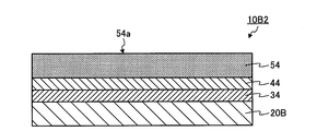
- the second stacked structure 10B2 is manufactured by a process different from the manufacturing of the first stacked structure 10A described above.
- the second electrode 34 is formed on one main surface of the second substrate 20B.
- the second charge transport layer 44 is formed on the second substrate 20B provided with the second electrode 34 in the same manner as the first charge transport layer 42.
- the second charge transport layer 44 is a hole transport layer when the second electrode 34 is an anode, and is an electron transport layer when the second electrode 34 is a cathode.
- the second substrate 20B, the second electrode 34 provided on the second substrate 20B, the second charge transport layer 44 provided on the second electrode 34, and the second charge transport layer 44 are provided.
- the second laminated structure 10B2 of the second embodiment including the second conductivity type layer 54 is manufactured.
- the first substrate 20A, the first electrode 32 provided on the first substrate 20A, the first charge transport layer 42 provided on the first electrode 32, and the first charge transport layer 42 are provided.
- the organic photoelectric conversion element that can be obtained by the manufacturing method according to the first embodiment and the second embodiment is a sealing material that is necessary for bonding the sealing substrate (second substrate) ( Therefore, the thickness of the entire element, in particular, the distance between the main surface of the first substrate and the main surface of the second substrate facing each other can be further reduced. Specifically, the distance between the main surface of the first substrate and the main surface of the second substrate facing each other, which was about 1 ⁇ m in the conventional configuration, is larger than 300 nm and smaller than 500 nm in the configuration of the present invention. It can be.
- Example 1 (Production of first laminated structure) A glass substrate (first substrate) having a 150 nm thick ITO thin film provided on one main surface by sputtering is washed with acetone, and then an ultraviolet ozone irradiation device (manufactured by Technovision) equipped with a low-pressure mercury lamp. , Model: UV-312) for 15 minutes by UV ozone cleaning to produce an ITO electrode (first electrode) having a clean surface. Next, TiO 2 (manufactured by Catalyst Kasei Co., Ltd., trade name PALSOL HPW) was applied on the ITO electrode surface by a spin coating method to form a TiO 2 layer (first charge transport layer).
- an ultraviolet ozone irradiation device manufactured by Technovision
- UV-312 UV-312
- TiO 2 manufactured by Catalyst Kasei Co., Ltd., trade name PALSOL HPW
- a first substrate provided with a first electrode, a charge transport layer, and an active layer, a second electrode, and a second substrate (second stacked structure) provided with a second electrode; Were stacked so that the active layer and the second charge transporting layer were in contact with each other in a sealed container under a chloroform saturated vapor pressure at 25 ° C. (normal temperature), and held under pressure for 30 minutes for bonding.
- the shape of the obtained organic photoelectric conversion element was a square of 2 mm ⁇ 2 mm.
Abstract
Description
〔1〕 第1基板、第2基板、該第1基板に設けられた第1電極及び該第2基板に設けられた第2電極からなる一対の電極、及び前記一対の電極間に挟持される活性層を備える、有機光電変換素子の製造方法において、前記第1基板に設けられた前記第1電極上に第1電荷輸送層を形成する工程と、前記第1電荷輸送層上に活性層を形成して第1積層構造体を形成する工程と、前記第2基板に設けられた前記第2電極上に第2電荷輸送層を形成して第2積層構造体を形成する工程と、前記第1積層構造体に設けられた活性層と前記第2積層構造体に設けられた第2電荷輸送層とを接触させ、前記第1積層構造体と前記第2積層構造体とを接合する接合工程とを含む、有機光電変換素子の製造方法。
〔2〕 第1基板、第2基板、該第1基板に設けられた第1電極及び該第2基板に設けられた第2電極からなる一対の電極、及び前記一対の電極間に挟持される活性層を備える、有機光電変換素子の製造方法において、前記第1基板に設けられた前記第1電極上に第1電荷輸送層を形成する工程と、前記第1電荷輸送層上に第1導電型層を形成して第1積層構造体を形成する工程と、前記第2基板に設けられた前記第2電極上に第2電荷輸送層を形成し、該第2電荷輸送層上に第2導電型層を形成して第2積層構造体を形成する工程と、前記第1導電型層と前記第2導電型層とを接触させて接合し、前記第1導電型層と前記第2導電型層とが積層された前記活性層を形成する接合工程とを含む、有機光電変換素子の製造方法。
〔3〕 接合工程が、第1基板及び第2基板のいずれか一方又は双方を押圧する加圧工程である、〔1〕又は〔2〕に記載の有機光電変換素子の製造方法。
〔4〕 接合工程が、常温よりも高温とした温度条件下で行われる、〔1〕~〔3〕のいずれか一項に記載の有機光電変換素子の製造方法。
〔5〕 接合工程が、40℃より高く100℃よりも低い温度条件下で行われる、〔4〕に記載の有機光電変換素子の製造方法。
〔6〕 接合工程が、第1積層構造体の第1基板とは反対側の露出層及び第2積層構造体の第2基板とは反対側の露出層のいずれか一方又双方の露出層の表面を溶解させる、溶媒蒸気雰囲気下で行われる、〔1〕~〔5〕のいずれか一項に記載の有機光電変換素子の製造方法。
〔7〕 溶媒蒸気として、芳香族炭化水素の蒸気又は脂肪族炭化水素の蒸気を用いる、〔6〕に記載の有機光電変換素子の製造方法。
〔8〕 溶媒蒸気として、水蒸気又はアルコールの蒸気を用いる、〔6〕に記載の有機光電変換素子の製造方法。
〔9〕 接合工程の後に、接合された第1積層構造体及び第2積層構造体を、真空中で真空処理する工程をさらに含む、〔1〕~〔8〕のいずれか一項に記載の有機光電変換素子の製造方法。
〔10〕 接合工程において、第1積層構造体の第1基板とは反対側の露出層及び第2積層構造体の第2基板とは反対側の露出層のいずれか一方又は双方が、有機化合物を含む層である、〔6〕~〔9〕のいずれか一項に記載の有機光電変換素子の製造方法。
〔11〕 接合工程において、第1積層構造体の第1基板とは反対側の露出層及び第2積層構造体の第2基板とは反対側の露出層のいずれか一方又は双方が、無機化合物を含む層である、〔6〕~〔9〕のいずれか一項に記載の有機光電変換素子の製造方法。
〔12〕 〔1〕~〔11〕のいずれか一項に記載の製造方法により製造することができる、有機光電変換素子。
〔13〕 対向する第1基板の主面と第2基板の主面との間隔が、300nmよりも大きく、かつ500nmよりも小さい、〔12〕に記載の有機光電変換素子。
〔14〕 第1基板及び第2基板のいずれか一方又は双方の基板が、無機化合物フィルムである、〔12〕又は〔13〕に記載の有機光電変換素子。
〔15〕 第1基板及び第2基板のいずれか一方又は双方の基板が、有機化合物フィルムである、〔12〕又は〔13〕に記載の有機光電変換素子。
〔16〕 無機化合物フィルムが、金属又は合金からなるフィルムである、〔14〕に記載の有機光電変換素子。
〔17〕 有機化合物フィルムが、バリア層をさらに有している、〔15〕に記載の有機光電変換素子。 That is, this invention provides the manufacturing method and organic photoelectric conversion element of the following organic photoelectric conversion element.
[1] A first substrate, a second substrate, a pair of electrodes including a first electrode provided on the first substrate and a second electrode provided on the second substrate, and sandwiched between the pair of electrodes In the method of manufacturing an organic photoelectric conversion element including an active layer, a step of forming a first charge transport layer on the first electrode provided on the first substrate, and an active layer on the first charge transport layer Forming a first stacked structure, forming a second charge transport layer on the second electrode provided on the second substrate to form a second stacked structure, A joining step of bringing the active layer provided in one laminated structure into contact with the second charge transport layer provided in the second laminated structure and joining the first laminated structure and the second laminated structure. The manufacturing method of an organic photoelectric conversion element containing these.
[2] A first substrate, a second substrate, a pair of electrodes including a first electrode provided on the first substrate and a second electrode provided on the second substrate, and sandwiched between the pair of electrodes In the method for manufacturing an organic photoelectric conversion element including an active layer, a step of forming a first charge transport layer on the first electrode provided on the first substrate, and a first conductivity on the first charge transport layer. Forming a first layered structure by forming a mold layer; forming a second charge transport layer on the second electrode provided on the second substrate; and forming a second charge transport layer on the second charge transport layer. A step of forming a second stacked structure by forming a conductive type layer, the first conductive type layer and the second conductive type layer are brought into contact with each other, and the first conductive type layer and the second conductive type are joined. And a bonding step of forming the active layer on which the mold layer is laminated.
[3] The method for producing an organic photoelectric conversion element according to [1] or [2], wherein the bonding step is a pressurizing step of pressing one or both of the first substrate and the second substrate.
[4] The method for producing an organic photoelectric conversion element according to any one of [1] to [3], wherein the bonding step is performed under temperature conditions higher than room temperature.
[5] The method for producing an organic photoelectric conversion element according to [4], wherein the bonding step is performed under a temperature condition higher than 40 ° C and lower than 100 ° C.
[6] In the bonding step, one or both of the exposed layer of the first laminated structure opposite to the first substrate and the exposed layer of the second laminated structure opposite to the second substrate are exposed. The method for producing an organic photoelectric conversion element according to any one of [1] to [5], which is carried out in a solvent vapor atmosphere in which the surface is dissolved.
[7] The method for producing an organic photoelectric conversion element according to [6], wherein an aromatic hydrocarbon vapor or an aliphatic hydrocarbon vapor is used as the solvent vapor.
[8] The method for producing an organic photoelectric conversion element according to [6], wherein water vapor or alcohol vapor is used as the solvent vapor.
[9] The method according to any one of [1] to [8], further including a step of vacuum-treating the joined first laminated structure and second laminated structure in a vacuum after the joining step. The manufacturing method of an organic photoelectric conversion element.
[10] In the bonding step, one or both of the exposed layer on the side opposite to the first substrate of the first stacked structure and the exposed layer on the side opposite to the second substrate of the second stacked structure are organic compounds. The method for producing an organic photoelectric conversion element according to any one of [6] to [9], wherein the organic photoelectric conversion element is a layer containing.
[11] In the bonding step, one or both of the exposed layer on the side opposite to the first substrate of the first stacked structure and the exposed layer on the side opposite to the second substrate of the second stacked structure are inorganic compounds. The method for producing an organic photoelectric conversion element according to any one of [6] to [9], wherein the organic photoelectric conversion element is a layer containing.
[12] An organic photoelectric conversion device that can be produced by the production method according to any one of [1] to [11].
[13] The organic photoelectric conversion element according to [12], wherein a distance between the main surface of the first substrate and the main surface of the second substrate facing each other is larger than 300 nm and smaller than 500 nm.
[14] The organic photoelectric conversion element according to [12] or [13], in which one or both of the first substrate and the second substrate are inorganic compound films.
[15] The organic photoelectric conversion element according to [12] or [13], in which one or both of the first substrate and the second substrate are organic compound films.
[16] The organic photoelectric conversion element according to [14], wherein the inorganic compound film is a film made of a metal or an alloy.
[17] The organic photoelectric conversion element according to [15], wherein the organic compound film further has a barrier layer.
10A:第1積層構造体
10B:第2積層構造体
20A:第1基板
20B:第2基板
32:第1電極
34:第2電極
42:第1電荷輸送層
44:第2電荷輸送層
50:活性層
52:第1導電型層
54:第2導電型層 DESCRIPTION OF SYMBOLS 10: Organic
以下、図面を参照して本発明を詳細に説明する。なお以下の説明において、各図は発明が理解できる程度に構成要素の形状、大きさ及び配置が概略的に示されているに過ぎず、これにより本発明が特に限定されるものではない。また各図において、同様の構成成分については同一の符号を付して示し、その重複する説明を省略する場合がある。 <Method for producing organic photoelectric conversion element>
Hereinafter, the present invention will be described in detail with reference to the drawings. In the following description, each drawing merely schematically shows the shape, size, and arrangement of constituent elements to the extent that the invention can be understood, and the present invention is not particularly limited thereby. Moreover, in each figure, about the same component, it attaches | subjects and shows the same code | symbol, The duplicate description may be abbreviate | omitted.
第1の実施形態の有機光電変換素子の製造方法は、第1基板に設けられた第1電極上に第1電荷輸送層を形成する工程と、第1電荷輸送層上に活性層を形成して第1積層構造体を形成する工程と、第2基板に設けられた第2電極上に第2電荷輸送層を形成して第2積層構造体を形成する工程と、第1積層構造体に設けられた活性層と第2積層構造体に設けられた第2電荷輸送層とを接触させ、第1積層構造体と第2積層構造体とを接合する接合工程とを含む。 (First embodiment)
The organic photoelectric conversion device manufacturing method of the first embodiment includes a step of forming a first charge transport layer on a first electrode provided on a first substrate, and an active layer formed on the first charge transport layer. Forming a first stacked structure, forming a second charge transport layer on a second electrode provided on the second substrate to form a second stacked structure, and A bonding step of bringing the active layer provided into contact with the second charge transporting layer provided in the second stacked structure and bonding the first stacked structure and the second stacked structure.
図1は、有機光電変換素子の製造方法を示す概略的な断面図(1)である。図2は、有機光電変換素子の製造方法を示す概略的な断面図(2)である。図4は、有機光電変換素子の構成を示す概略的な断面図(1)である。 Here, with reference to FIG.1, FIG2 and FIG.4, the manufacturing method of the organic photoelectric conversion element of 1st Embodiment is demonstrated concretely.
FIG. 1 is a schematic cross-sectional view (1) illustrating a method for producing an organic photoelectric conversion element. FIG. 2 is a schematic cross-sectional view (2) illustrating the method for producing the organic photoelectric conversion element. FIG. 4 is a schematic cross-sectional view (1) showing the configuration of the organic photoelectric conversion element.
第1基板20Aの材料の例としては、ガラス、プラスチック、高分子フィルム、シリコン等が挙げられる。 The material of the
Examples of the material of the
第1電極32及び後述する第2電極34のうち、少なくとも光が入射する側の電極、すなわち少なくとも一方の電極は、発電に必要な波長の入射光(太陽光)を透過させことができる透明又は半透明の電極とされる。
第1基板20Aが入射光を不透過とする不透明である場合には、第1電極32と対向する、第1基板20Aとは反対側に設けられることとなる第2基板20B及び第2電極32を透明とするか、又は所要の入射光を透過できる半透明とする必要がある。 If the
Of the
When the
電極の作製方法の例としては、真空蒸着法、スパッタリング法、イオンプレーティング法、メッキ法等が挙げられる。また、電極として、ポリアニリン及びその誘導体、ポリチオフェン及びその誘導体等の有機の透明導電膜を用いてもよい。 Examples of the transparent or translucent electrode include a conductive metal oxide film and a translucent metal thin film. Specifically, as an electrode that is transparent or translucent, a conductive material of indium oxide, zinc oxide, tin oxide, and indium tin oxide or indium zinc oxide (IZO) that is a composite thereof is used. Films made, such as NESA, gold, platinum, silver, copper, etc. are used, and ITO, IZO, and tin oxide films are preferred.
Examples of the electrode manufacturing method include a vacuum deposition method, a sputtering method, an ion plating method, a plating method, and the like. Moreover, you may use organic transparent conductive films, such as polyaniline and its derivative (s), polythiophene, and its derivative (s) as an electrode.
第1電荷輸送層42は、第1電極32が陽極である場合には正孔輸送層であり、また第1電極32が陰極である場合には電子輸送層である。
第1電荷輸送層42の材料の例としては、フッ化リチウム等のアルカリ金属及びアルカリ土類金属のハロゲン化物、アルカリ金属及びアルカリ土類金属の酸化物等を用いることができる。また、酸化チタン等無機半導体の微粒子、PEDOT(ポリ-3,4-エチレンジオキシチオフェン)などが挙げられる。 Next, the first
The first
Examples of the material of the first
なお、電子供与性化合物と電子受容性化合物とは、これらの化合物のエネルギー準位のエネルギーレベルから相対的に決定され、1つの化合物が電子供与性化合物、電子受容性化合物のいずれともなり得る。 As described above, the
Note that the electron-donating compound and the electron-accepting compound are determined relatively from the energy levels of these compounds, and one compound can be either an electron-donating compound or an electron-accepting compound.


第2電荷輸送層44は、第2電極34が陽極である場合には正孔輸送層であり、第2電極34が陰極である場合には電子輸送層である。 Next, the second
The second
加圧工程は、例えば液晶表示パネルの製造工程における貼り合わせ工程に用いられるような従来公知の加圧定盤を備える加圧装置を用いて、第1基板20A及び第2基板20Bのいずれか一方又は双方の露出している主面側から圧力を加える押圧工程により、第1積層構造体10Aと第2積層構造体10B1とが一体化するように貼り合わせることができる。圧力の程度としては、層構造が破壊されず、かつ安定した接合強度を確保できることを条件として任意好適な圧力で実施することができる。 This joining process is performed by, for example, a pressurizing process for pressing one or both of the
The pressurizing process uses either a
このように接合面である露出層の表面を溶解させた状態で接合工程を行うことにより、層同士の親和性が向上するため、接合強度をより向上させることができる。 The solvent vapor can be any suitable solvent vapor depending on the material of the exposed layer. As the material for the solvent vapor, when the exposed layer is an active layer, aromatic hydrocarbon compounds such as chloroform, toluene, xylene, chlorobenzene, and the exposed layer material are water-soluble materials such as PEDOT: PSS. In some cases, it is preferred to use water, alcohols such as methanol, ethanol, isopropyl alcohol or mixtures thereof.
Thus, by performing a joining process in the state which dissolved the surface of the exposed layer which is a joining surface, since the affinity of layers improves, joining strength can be improved more.
第2の実施形態の有機光電変換素子の製造方法は、第1基板に設けられた第1電極及び第2基板に設けられた第2電極からなる一対の電極、及び一対の電極間に挟持される活性層を備える、有機光電変換素子の製造方法において、第1基板に設けられた第1電極上に第1電荷輸送層を形成する工程と、第1電荷輸送層上に第1導電型層を形成して第1積層構造体を形成する工程と、第2基板に設けられた第2電極上に第2電荷輸送層を形成し、第2電荷輸送層上に第2導電型層を形成して第2積層構造体を形成する工程と、第1導電型層と第2導電型層とを接触させて接合し、第1導電型層と第2導電型層とが積層された活性層を形成する接合工程とを備える。 (Second Embodiment)
In the organic photoelectric conversion element manufacturing method according to the second embodiment, a pair of electrodes including a first electrode provided on a first substrate and a second electrode provided on a second substrate, and the pair of electrodes are sandwiched between the pair of electrodes. In the method for manufacturing an organic photoelectric conversion element, the first charge transport layer is formed on the first electrode provided on the first substrate, and the first conductivity type layer is formed on the first charge transport layer. Forming a first stacked structure, forming a second charge transport layer on the second electrode provided on the second substrate, and forming a second conductivity type layer on the second charge transport layer Then, the step of forming the second laminated structure and the active layer in which the first conductivity type layer and the second conductivity type layer are brought into contact with each other and bonded, and the first conductivity type layer and the second conductivity type layer are laminated. A bonding step of forming
図1は、有機光電変換素子の製造方法を示す概略的な断面図(1)である。図3は、有機光電変換素子の製造方法を示す概略的な断面図(3)である。図5は、有機光電変換素子の構成を示す概略的な断面図(2)である。 Here, with reference to FIG.1, FIG3 and FIG.5, the manufacturing method of the organic photoelectric conversion element of 2nd Embodiment is demonstrated concretely. The same configurations as those in the first embodiment already described may be denoted by the same reference numerals, and detailed description thereof may be omitted, and the same processes as those in the first embodiment may be described in details such as conditions. May be omitted.
FIG. 1 is a schematic cross-sectional view (1) illustrating a method for producing an organic photoelectric conversion element. FIG. 3: is schematic sectional drawing (3) which shows the manufacturing method of an organic photoelectric conversion element. FIG. 5 is a schematic cross-sectional view (2) showing the configuration of the organic photoelectric conversion element.
第2の実施の形態の製造方法では、露出層が第1導電型層52及び第2導電型層54であるため、製造される有機光電素子は、pnヘテロ接合(pnヘテロジャンクション)型となる。 As shown in FIG. 5, the manufactured first
In the manufacturing method of the second embodiment, since the exposed layers are the first
ここで本発明の製造方法により製造される有機光電変換素子について説明する。有機光電変換素子のとりうる層構成の一例を以下に示す。
a)陽極/活性層/陰極
b)陽極/正孔輸送層/活性層/陰極
c)陽極/活性層/電子輸送層/陰極
d)陽極/正孔輸送層/活性層/電子輸送層/陰極
e)陽極/電子供給性層/電子受容性層/陰極
f)陽極/正孔輸送層/電子供給性層/電子受容性層/陰極
g)陽極/電子供給性層/電子受容性層/電子輸送層/陰極
h)陽極/正孔輸送層/電子供給性層/電子受容性層/電子輸送層/陰極
(ここで、記号「/」は、記号「/」を挟む層同士が隣接して積層されていることを示す。) <Organic photoelectric conversion element>
Here, the organic photoelectric conversion element manufactured by the manufacturing method of the present invention will be described. An example of the layer structure that the organic photoelectric conversion element can take is shown below.
a) Anode / active layer / cathode b) Anode / hole transport layer / active layer / cathode c) Anode / active layer / electron transport layer / cathode d) Anode / hole transport layer / active layer / electron transport layer / cathode e) Anode / electron supply layer / electron acceptor layer / cathode f) Anode / hole transport layer / electron supply layer / electron acceptor layer / cathode g) Anode / electron supply layer / electron acceptor layer / electron Transport layer / cathode h) anode / hole transport layer / electron supply layer / electron-accepting layer / electron transport layer / cathode (where the symbol “/” is adjacent to the layer sandwiching the symbol “/”) Indicates that they are stacked.)
電子受容性化合物及び電子供与性化合物を含有するバルクヘテロ型の活性層を有する有機光電変換素子における電子受容性化合物の割合は、電子供与性化合物100重量部に対して、10重量部~1000重量部とすることが好ましく、50重量部~500重量部とすることがより好ましい。 Each of the above layers may be formed as a single layer or a laminate of two or more layers.
The ratio of the electron accepting compound in the organic photoelectric conversion device having the bulk hetero type active layer containing the electron accepting compound and the electron donating compound is 10 parts by weight to 1000 parts by weight with respect to 100 parts by weight of the electron donating compound. It is preferably 50 parts by weight to 500 parts by weight.
また、2枚の基板を独立に処理した後で貼り合わせるため、製造工程が簡易となり、また2枚の基板に挟まれた電極、電荷輸送層、活性層のような機能層の組み合わせの変更が容易となるため、多品種の有機光電変換素子の製造が必要な場合でも容易に対応することができる。 According to the method for producing an organic photoelectric conversion element of the present invention, the active layer and the like can be produced without being exposed to a high temperature. Therefore, it is possible to avoid deterioration of electrical characteristics and loss of function due to the high temperature treatment.
In addition, since the two substrates are independently processed and bonded together, the manufacturing process is simplified, and the combination of functional layers such as electrodes, charge transport layers, and active layers sandwiched between the two substrates can be changed. Since it becomes easy, it can respond easily even when manufacture of many kinds of organic photoelectric conversion elements is required.
本発明の製造方法により製造される有機光電変換素子は、透明又は半透明の電極である第1電極及び/又は第2電極から太陽光等の光を照射することにより、電極間に光起電力が発生し、有機薄膜太陽電池として動作させることができる。有機薄膜太陽電池を複数集積することにより有機薄膜太陽電池モジュールとして用いることもできる。 <Application>
The organic photoelectric conversion element manufactured by the manufacturing method of the present invention irradiates light such as sunlight from the first electrode and / or the second electrode, which are transparent or translucent electrodes, so that the photovoltaic power is generated between the electrodes. Is generated and can be operated as an organic thin film solar cell. It can also be used as an organic thin film solar cell module by integrating a plurality of organic thin film solar cells.
(第1積層構造体の作製)
スパッタリング法により150nmの厚みでITOの薄膜が一方の主面に設けられたガラス基板(第1基板)を、アセトンにて洗浄した後、低圧水銀ランプを備えた紫外線オゾン照射装置(テクノビジョン社製、型式:UV-312)を用いて15分間、UVオゾン洗浄処理し、清浄な表面をもつITO電極(第1電極)を作製した。次いで、ITO電極表面上にTiO2(触媒化成社製、商品名PALSOL HPW)をスピンコート法により塗布してTiO2層(第1電荷輸送層)を形成した。その後、大気中、150℃で40分間乾燥を行った。電子供与性化合物であるポリ(3-ヘキシルチオフェン)(P3HT)(メルク社製、商品名lisicon SP001、lot.EF431002)と、電子受容性化合物であるフラーレン誘導体としてPCBM(フロンティアカーボン社製、商品名E100、lot.7B0168-A)とを、オルトジクロロベンゼン溶媒中にP3HTが1.5重量%、PCBMが2重量%となるように添加し、70℃で2時間撹拌を行なった後、孔径0.2μmのフィルタにてろ過を行い、塗工液を調製した。TiO2層上に、塗工液をスピンコート法により塗布し、窒素ガス雰囲気下において、150℃で3分間加熱処理して活性層を成膜した。加熱処理後の活性層の膜厚は約100nmであった。 <Example 1>
(Production of first laminated structure)
A glass substrate (first substrate) having a 150 nm thick ITO thin film provided on one main surface by sputtering is washed with acetone, and then an ultraviolet ozone irradiation device (manufactured by Technovision) equipped with a low-pressure mercury lamp. , Model: UV-312) for 15 minutes by UV ozone cleaning to produce an ITO electrode (first electrode) having a clean surface. Next, TiO 2 (manufactured by Catalyst Kasei Co., Ltd., trade name PALSOL HPW) was applied on the ITO electrode surface by a spin coating method to form a TiO 2 layer (first charge transport layer). Thereafter, drying was performed in air at 150 ° C. for 40 minutes. Poly (3-hexylthiophene) (P3HT) (trade name, licicon SP001, lot. EF431002), which is an electron-donating compound, and PCBM (frontier carbon, trade name, which is an electron-accepting compound). E100, lot.7B0168-A) was added to an orthodichlorobenzene solvent so that P3HT was 1.5 wt% and PCBM was 2 wt%, and the mixture was stirred at 70 ° C. for 2 hours. The solution was filtered through a 2 μm filter to prepare a coating solution. A coating solution was applied onto the TiO 2 layer by a spin coating method, and an active layer was formed by heat treatment at 150 ° C. for 3 minutes in a nitrogen gas atmosphere. The film thickness of the active layer after the heat treatment was about 100 nm.
ガラス基板(第2基板)をアセトンにて洗浄した後、低圧水銀ランプを備えた紫外線オゾン照射装置を用いて、15分間、UVオゾン洗浄処理した。次いで、ガラス基板上にAgペースト(三ツ星ベルト社製、商品名:MDot-SLP)をスクリーン印刷法により塗布した後、大気中、200℃で30分間熱処理して第2電極を形成して、第2積層構造体とした。加熱処理後のAg層の膜厚は約5μmであった。次いで、Ag層上にPEDOT層(スタルク社製、商品名 Baytron P AI4083、lot.HCD0701019)をスピンコート法により塗布してPEDOT層(第2電荷輸送層)を形成した。その後、大気中、150℃で30分間乾燥を行った。 (Production of second laminated structure)
After the glass substrate (second substrate) was cleaned with acetone, UV ozone cleaning treatment was performed for 15 minutes using an ultraviolet ozone irradiation apparatus equipped with a low-pressure mercury lamp. Next, an Ag paste (trade name: MDot-SLP, manufactured by Mitsuboshi Belting Co., Ltd.) is applied on a glass substrate by a screen printing method, and then heat treated at 200 ° C. for 30 minutes in the atmosphere to form a second electrode. A two-layer structure was obtained. The film thickness of the Ag layer after the heat treatment was about 5 μm. Next, a PEDOT layer (second trade charge Baytron P AI4083, lot. HCD0701019) was applied by spin coating on the Ag layer to form a PEDOT layer (second charge transport layer). Thereafter, drying was performed in air at 150 ° C. for 30 minutes.
第1電極、電荷輸送層、及び活性層が設けられた第1基板(第1積層構造体)と、第2電極と、第2電極が設けられた第2基板(第2積層構造体)とを、25℃(常温)、クロロホルム飽和蒸気圧下の密閉容器内で、活性層と第2電荷輸送層とが接触するように重ね合わせ、加圧状態で30分間保持して接合した。得られた有機光電変換素子の形状は、2mm×2mmの正方形であった。 (Production of organic photoelectric conversion element)
A first substrate (first stacked structure) provided with a first electrode, a charge transport layer, and an active layer, a second electrode, and a second substrate (second stacked structure) provided with a second electrode; Were stacked so that the active layer and the second charge transporting layer were in contact with each other in a sealed container under a chloroform saturated vapor pressure at 25 ° C. (normal temperature), and held under pressure for 30 minutes for bonding. The shape of the obtained organic photoelectric conversion element was a square of 2 mm × 2 mm.
(光電変換効率の測定)
実施例1で作製された有機光電変換素子の光電変換効率をソーラシミュレータ(山下電装社製、商品名YSS-80)を用い、AM1.5Gフィルタを通した放射照度100mW/cm2の光を照射し、電流及び電圧を測定した結果、発電が認められた。 <Evaluation>
(Measurement of photoelectric conversion efficiency)
Using a solar simulator (trade name: YSS-80, manufactured by Yamashita Denso Co., Ltd.), the photoelectric conversion efficiency of the organic photoelectric conversion element manufactured in Example 1 was irradiated with light having an irradiance of 100 mW / cm 2 through an AM1.5G filter. As a result of measuring the current and voltage, power generation was observed.
Claims (17)
- 第1基板、第2基板、該第1基板に設けられた第1電極及び該第2基板に設けられた第2電極からなる一対の電極、並びに前記一対の電極間に挟持される活性層を備える、有機光電変換素子の製造方法において、
前記第1基板に設けられた前記第1電極上に第1電荷輸送層を形成する工程と、
前記第1電荷輸送層上に活性層を形成して第1積層構造体を形成する工程と、
前記第2基板に設けられた前記第2電極上に第2電荷輸送層を形成して第2積層構造体を形成する工程と、
前記第1積層構造体に設けられた前記活性層と前記第2積層構造体に設けられた前記第2電荷輸送層とを接触させ、前記第1積層構造体と前記第2積層構造体とを接合する接合工程と
を含む、有機光電変換素子の製造方法。 A first substrate, a second substrate, a pair of electrodes including a first electrode provided on the first substrate and a second electrode provided on the second substrate, and an active layer sandwiched between the pair of electrodes In the method for producing an organic photoelectric conversion element,
Forming a first charge transport layer on the first electrode provided on the first substrate;
Forming an active layer on the first charge transport layer to form a first stacked structure;
Forming a second charge transport layer on the second electrode provided on the second substrate to form a second stacked structure;
The active layer provided in the first stacked structure and the second charge transport layer provided in the second stacked structure are brought into contact with each other, and the first stacked structure and the second stacked structure are The manufacturing method of an organic photoelectric conversion element including the joining process to join. - 第1基板、第2基板、該第1基板に設けられた第1電極及び該第2基板に設けられた第2電極からなる一対の電極、並びに前記一対の電極間に挟持される活性層を備える、有機光電変換素子の製造方法において、
前記第1基板に設けられた前記第1電極上に第1電荷輸送層を形成する工程と、
前記第1電荷輸送層上に第1導電型層を形成して第1積層構造体を形成する工程と、
前記第2基板に設けられた第2電極上に第2電荷輸送層を形成し、該第2電荷輸送層上に第2導電型層を形成して第2積層構造体を形成する工程と、
前記第1導電型層と前記第2導電型層とを接触させて接合し、前記第1導電型層と前記第2導電型層とが積層された前記活性層を形成する接合工程と
を含む、有機光電変換素子の製造方法。 A first substrate, a second substrate, a pair of electrodes including a first electrode provided on the first substrate and a second electrode provided on the second substrate, and an active layer sandwiched between the pair of electrodes In the method for producing an organic photoelectric conversion element,
Forming a first charge transport layer on the first electrode provided on the first substrate;
Forming a first stacked structure by forming a first conductivity type layer on the first charge transport layer;
Forming a second charge transport layer on the second electrode provided on the second substrate, forming a second conductivity type layer on the second charge transport layer, and forming a second stacked structure;
Joining the first conductivity type layer and the second conductivity type layer in contact with each other to form the active layer in which the first conductivity type layer and the second conductivity type layer are stacked. The manufacturing method of an organic photoelectric conversion element. - 接合工程が、第1基板及び第2基板のいずれか一方又は双方を押圧する加圧工程である、請求項1に記載の有機光電変換素子の製造方法。 The method for producing an organic photoelectric conversion element according to claim 1, wherein the bonding step is a pressurizing step of pressing either one or both of the first substrate and the second substrate.
- 接合工程が、常温よりも高温とした温度条件下で行われる、請求項1に記載の有機光電変換素子の製造方法。 The method for producing an organic photoelectric conversion element according to claim 1, wherein the joining step is performed under temperature conditions higher than room temperature.
- 接合工程が、40℃より高く100℃よりも低い温度条件下で行われる、請求項4に記載の有機光電変換素子の製造方法。 The method for producing an organic photoelectric conversion element according to claim 4, wherein the joining step is performed under a temperature condition higher than 40 ° C and lower than 100 ° C.
- 接合工程が、第1積層構造体の第1基板とは反対側の露出層及び第2積層構造体の第2基板とは反対側の露出層のいずれか一方又双方の露出層の表面を溶解させる、溶媒蒸気雰囲気下で行われる、請求項1に記載の有機光電変換素子の製造方法。 The bonding step dissolves the surface of one or both of the exposed layer on the side opposite to the first substrate of the first laminated structure and the exposed layer on the side opposite to the second substrate of the second laminated structure. The manufacturing method of the organic photoelectric conversion element of Claim 1 performed in the solvent vapor | steam atmosphere.
- 溶媒蒸気として、芳香族炭化水素の蒸気又は脂肪族炭化水素の蒸気を用いる、請求項6に記載の有機光電変換素子の製造方法。 The method for producing an organic photoelectric conversion element according to claim 6, wherein an aromatic hydrocarbon vapor or an aliphatic hydrocarbon vapor is used as the solvent vapor.
- 溶媒蒸気として、水蒸気又はアルコールの蒸気を用いる、請求項6に記載の有機光電変換素子の製造方法。 The method for producing an organic photoelectric conversion element according to claim 6, wherein water vapor or alcohol vapor is used as the solvent vapor.
- 接合工程の後に、接合された第1積層構造体及び第2積層構造体を、真空中で真空処理する工程をさらに含む、請求項1に記載の有機光電変換素子の製造方法。 The manufacturing method of the organic photoelectric conversion element of Claim 1 which further includes the process of vacuum-processing the joined 1st laminated structure and 2nd laminated structure in a vacuum after a joining process.
- 接合工程において、第1積層構造体の第1基板とは反対側の露出層及び第2積層構造体の第2基板とは反対側の露出層のいずれか一方又は双方が、有機化合物を含む層である、請求項6に記載の有機光電変換素子の製造方法。 In the bonding step, one or both of the exposed layer on the side opposite to the first substrate of the first stacked structure and the exposed layer on the side opposite to the second substrate of the second stacked structure include a layer containing an organic compound. The manufacturing method of the organic photoelectric conversion element of Claim 6 which is.
- 接合工程において、第1積層構造体の第1基板とは反対側の露出層及び第2積層構造体の第2基板とは反対側の露出層のいずれか一方又は双方が、無機化合物を含む層である、請求項6に記載の有機光電変換素子の製造方法。 In the bonding step, one or both of the exposed layer on the side opposite to the first substrate of the first stacked structure and the exposed layer on the side opposite to the second substrate of the second stacked structure include a layer containing an inorganic compound. The manufacturing method of the organic photoelectric conversion element of Claim 6 which is.
- 請求項1に記載の製造方法により製造することができる、有機光電変換素子。 An organic photoelectric conversion element that can be produced by the production method according to claim 1.
- 対向する第1基板の主面と第2基板の主面との間隔が、300nmよりも大きく、かつ500nmよりも小さい、請求項12に記載の有機光電変換素子。 The organic photoelectric conversion element according to claim 12, wherein a distance between the main surface of the first substrate and the main surface of the second substrate facing each other is larger than 300 nm and smaller than 500 nm.
- 第1基板及び第2基板のいずれか一方又は双方の基板が、無機化合物フィルムである、請求項12に記載の有機光電変換素子。 The organic photoelectric conversion element according to claim 12, wherein one or both of the first substrate and the second substrate are inorganic compound films.
- 第1基板及び第2基板のいずれか一方又は双方の基板が、有機化合物フィルムである、請求項12に記載の有機光電変換素子。 The organic photoelectric conversion element according to claim 12, wherein one or both of the first substrate and the second substrate are organic compound films.
- 無機化合物フィルムが、金属又は合金からなるフィルムである、請求項14に記載の有機光電変換素子。 The organic photoelectric conversion element according to claim 14, wherein the inorganic compound film is a film made of a metal or an alloy.
- 有機化合物フィルムが、バリア層をさらに有している、請求項15に記載の有機光電変換素子。 The organic photoelectric conversion element according to claim 15, wherein the organic compound film further has a barrier layer.
Priority Applications (2)
| Application Number | Priority Date | Filing Date | Title |
|---|---|---|---|
| CN2010800470134A CN102576806A (en) | 2009-10-30 | 2010-10-22 | Method for production of organic photoelectric conversion element |
| US13/504,733 US20120216868A1 (en) | 2009-10-30 | 2010-10-22 | Manufacturing method of organic photovoltaic cell |
Applications Claiming Priority (2)
| Application Number | Priority Date | Filing Date | Title |
|---|---|---|---|
| JP2009-251248 | 2009-10-30 | ||
| JP2009251248 | 2009-10-30 |
Publications (1)
| Publication Number | Publication Date |
|---|---|
| WO2011052509A1 true WO2011052509A1 (en) | 2011-05-05 |
Family
ID=43921931
Family Applications (1)
| Application Number | Title | Priority Date | Filing Date |
|---|---|---|---|
| PCT/JP2010/068732 WO2011052509A1 (en) | 2009-10-30 | 2010-10-22 | Method for production of organic photoelectric conversion element |
Country Status (4)
| Country | Link |
|---|---|
| US (1) | US20120216868A1 (en) |
| JP (1) | JP2011119680A (en) |
| CN (1) | CN102576806A (en) |
| WO (1) | WO2011052509A1 (en) |
Families Citing this family (5)
| Publication number | Priority date | Publication date | Assignee | Title |
|---|---|---|---|---|
| JP5936186B2 (en) * | 2012-03-14 | 2016-06-15 | 日立造船株式会社 | Manufacturing method of solar cell |
| JP2013222750A (en) * | 2012-04-13 | 2013-10-28 | Kuraray Co Ltd | Photoelectric conversion element, method for manufacturing the same, and solar cell |
| CN104916782B (en) * | 2015-05-25 | 2017-10-24 | 中国科学院半导体研究所 | Using the inversion solar battery structure and preparation method of surface phasmon effect |
| CN109244260B (en) * | 2018-09-19 | 2021-01-29 | 京东方科技集团股份有限公司 | Preparation method of display panel |
| CN112352327A (en) * | 2019-03-19 | 2021-02-09 | 株式会社东芝 | Photoelectric conversion element and method for manufacturing photoelectric conversion element |
Citations (6)
| Publication number | Priority date | Publication date | Assignee | Title |
|---|---|---|---|---|
| JPH05145098A (en) * | 1991-09-13 | 1993-06-11 | Toyo Kako Kk | Photovoltaic organic photoelectric conversion element |
| JPH05275728A (en) * | 1992-03-26 | 1993-10-22 | Ricoh Co Ltd | Organic photovoltaic element |
| JP2002508599A (en) * | 1998-03-20 | 2002-03-19 | ケンブリッジ ディスプレイ テクノロジー リミテッド | Multilayer photovoltaic element or photoconductive element and method for manufacturing the same |
| JP2005538555A (en) * | 2002-09-05 | 2005-12-15 | コナルカ テクノロジーズ インコーポレイテッド | Photovoltaic active layer and organic photovoltaic device processing method |
| JP2006344741A (en) * | 2005-06-08 | 2006-12-21 | Sharp Corp | Organic solar cell and its manufacturing method |
| JP2009076241A (en) * | 2007-09-19 | 2009-04-09 | Konica Minolta Holdings Inc | Manufacturing method of organic electroluminescent element |
Family Cites Families (11)
| Publication number | Priority date | Publication date | Assignee | Title |
|---|---|---|---|---|
| US7449629B2 (en) * | 2002-08-21 | 2008-11-11 | Truseal Technologies, Inc. | Solar panel including a low moisture vapor transmission rate adhesive composition |
| JP2004247161A (en) * | 2003-02-13 | 2004-09-02 | Morio Taniguchi | Manufacturing method of organic electroluminescent element |
| JP4496359B2 (en) * | 2003-03-25 | 2010-07-07 | 国立大学法人信州大学 | Method for manufacturing organic electroluminescence display panel |
| US7063994B2 (en) * | 2003-07-11 | 2006-06-20 | Organic Vision Inc. | Organic semiconductor devices and methods of fabrication including forming two parts with polymerisable groups and bonding the parts |
| GB2416621A (en) * | 2004-07-27 | 2006-02-01 | Cambridge Display Tech Ltd | Laminated interconnects for opto-electronic device modules |
| US7625596B2 (en) * | 2004-12-15 | 2009-12-01 | General Electric Company | Adhesion promoter, electroactive layer and electroactive device comprising same, and method |
| JP2006332380A (en) * | 2005-05-26 | 2006-12-07 | Matsushita Electric Works Ltd | Organic solar cell and manufacturing method thereof |
| JP2008091575A (en) * | 2006-09-29 | 2008-04-17 | Dainippon Printing Co Ltd | Organic thin film solar cell element and coating liquid for forming photoelectric conversion layer |
| US8952247B2 (en) * | 2007-07-09 | 2015-02-10 | Mitsubishi Chemical Corporation | Photoelectric converter and solar cell using the same |
| US8044389B2 (en) * | 2007-07-27 | 2011-10-25 | The Regents Of The University Of California | Polymer electronic devices by all-solution process |
| JP5287137B2 (en) * | 2008-10-22 | 2013-09-11 | コニカミノルタ株式会社 | Manufacturing method of organic photoelectric conversion element |
-
2010
- 2010-10-22 CN CN2010800470134A patent/CN102576806A/en active Pending
- 2010-10-22 WO PCT/JP2010/068732 patent/WO2011052509A1/en active Application Filing
- 2010-10-22 US US13/504,733 patent/US20120216868A1/en not_active Abandoned
- 2010-10-27 JP JP2010240926A patent/JP2011119680A/en active Pending
Patent Citations (6)
| Publication number | Priority date | Publication date | Assignee | Title |
|---|---|---|---|---|
| JPH05145098A (en) * | 1991-09-13 | 1993-06-11 | Toyo Kako Kk | Photovoltaic organic photoelectric conversion element |
| JPH05275728A (en) * | 1992-03-26 | 1993-10-22 | Ricoh Co Ltd | Organic photovoltaic element |
| JP2002508599A (en) * | 1998-03-20 | 2002-03-19 | ケンブリッジ ディスプレイ テクノロジー リミテッド | Multilayer photovoltaic element or photoconductive element and method for manufacturing the same |
| JP2005538555A (en) * | 2002-09-05 | 2005-12-15 | コナルカ テクノロジーズ インコーポレイテッド | Photovoltaic active layer and organic photovoltaic device processing method |
| JP2006344741A (en) * | 2005-06-08 | 2006-12-21 | Sharp Corp | Organic solar cell and its manufacturing method |
| JP2009076241A (en) * | 2007-09-19 | 2009-04-09 | Konica Minolta Holdings Inc | Manufacturing method of organic electroluminescent element |
Also Published As
| Publication number | Publication date |
|---|---|
| US20120216868A1 (en) | 2012-08-30 |
| JP2011119680A (en) | 2011-06-16 |
| CN102576806A (en) | 2012-07-11 |
Similar Documents
| Publication | Publication Date | Title |
|---|---|---|
| JP5553727B2 (en) | Organic photoelectric conversion device and manufacturing method thereof | |
| JP5715795B2 (en) | Manufacturing method of organic thin film solar cell module | |
| JP5663264B2 (en) | Manufacturing method of organic thin film solar cell module | |
| WO2011052568A1 (en) | Organic photoelectric conversion element | |
| WO2011052509A1 (en) | Method for production of organic photoelectric conversion element | |
| WO2011052510A1 (en) | Organic thin film solar cell and method for manufacturing same | |
| WO2010024157A1 (en) | Organic photoelectric conversion element and fabrication method therefor | |
| WO2011052583A1 (en) | Organic photoelectric conversion element | |
| WO2011052569A1 (en) | Organic photoelectric conversion element | |
| WO2011052546A1 (en) | Organic photoelectric conversion element and manufacturing method thereof | |
| US20120216869A1 (en) | Organic photovoltaic cell and method for manufacturing the same | |
| JP5715796B2 (en) | Manufacturing method of organic photoelectric conversion element | |
| JP2015099810A (en) | Method of manufacturing organic photoelectric conversion element | |
| JP5932928B2 (en) | Photoelectric conversion device | |
| WO2011101993A1 (en) | Solar cell and method for manufacturing same | |
| US9318719B2 (en) | Method of producing organic photoelectric conversion device | |
| JP6743812B2 (en) | Organic photoelectric conversion element | |
| WO2011052578A1 (en) | Process for production of organic photoelectric conversion element |
Legal Events
| Date | Code | Title | Description |
|---|---|---|---|
| WWE | Wipo information: entry into national phase |
Ref document number: 201080047013.4 Country of ref document: CN |
|
| 121 | Ep: the epo has been informed by wipo that ep was designated in this application |
Ref document number: 10826641 Country of ref document: EP Kind code of ref document: A1 |
|
| WWE | Wipo information: entry into national phase |
Ref document number: 13504733 Country of ref document: US |
|
| NENP | Non-entry into the national phase |
Ref country code: DE |
|
| 122 | Ep: pct application non-entry in european phase |
Ref document number: 10826641 Country of ref document: EP Kind code of ref document: A1 |