WO2011037040A1 - Imaging device - Google Patents
Imaging device Download PDFInfo
- Publication number
- WO2011037040A1 WO2011037040A1 PCT/JP2010/065811 JP2010065811W WO2011037040A1 WO 2011037040 A1 WO2011037040 A1 WO 2011037040A1 JP 2010065811 W JP2010065811 W JP 2010065811W WO 2011037040 A1 WO2011037040 A1 WO 2011037040A1
- Authority
- WO
- WIPO (PCT)
- Prior art keywords
- data
- field
- pixel
- pixels
- control signal
- Prior art date
Links
Images


Classifications
-
- H—ELECTRICITY
- H04—ELECTRIC COMMUNICATION TECHNIQUE
- H04N—PICTORIAL COMMUNICATION, e.g. TELEVISION
- H04N25/00—Circuitry of solid-state image sensors [SSIS]; Control thereof
-
- H—ELECTRICITY
- H04—ELECTRIC COMMUNICATION TECHNIQUE
- H04N—PICTORIAL COMMUNICATION, e.g. TELEVISION
- H04N25/00—Circuitry of solid-state image sensors [SSIS]; Control thereof
- H04N25/40—Extracting pixel data from image sensors by controlling scanning circuits, e.g. by modifying the number of pixels sampled or to be sampled
- H04N25/44—Extracting pixel data from image sensors by controlling scanning circuits, e.g. by modifying the number of pixels sampled or to be sampled by partially reading an SSIS array
- H04N25/447—Extracting pixel data from image sensors by controlling scanning circuits, e.g. by modifying the number of pixels sampled or to be sampled by partially reading an SSIS array by preserving the colour pattern with or without loss of information
-
- H—ELECTRICITY
- H04—ELECTRIC COMMUNICATION TECHNIQUE
- H04N—PICTORIAL COMMUNICATION, e.g. TELEVISION
- H04N25/00—Circuitry of solid-state image sensors [SSIS]; Control thereof
- H04N25/10—Circuitry of solid-state image sensors [SSIS]; Control thereof for transforming different wavelengths into image signals
- H04N25/11—Arrangement of colour filter arrays [CFA]; Filter mosaics
- H04N25/13—Arrangement of colour filter arrays [CFA]; Filter mosaics characterised by the spectral characteristics of the filter elements
- H04N25/134—Arrangement of colour filter arrays [CFA]; Filter mosaics characterised by the spectral characteristics of the filter elements based on three different wavelength filter elements
-
- H—ELECTRICITY
- H04—ELECTRIC COMMUNICATION TECHNIQUE
- H04N—PICTORIAL COMMUNICATION, e.g. TELEVISION
- H04N25/00—Circuitry of solid-state image sensors [SSIS]; Control thereof
- H04N25/40—Extracting pixel data from image sensors by controlling scanning circuits, e.g. by modifying the number of pixels sampled or to be sampled
- H04N25/42—Extracting pixel data from image sensors by controlling scanning circuits, e.g. by modifying the number of pixels sampled or to be sampled by switching between different modes of operation using different resolutions or aspect ratios, e.g. switching between interlaced and non-interlaced mode
-
- H—ELECTRICITY
- H04—ELECTRIC COMMUNICATION TECHNIQUE
- H04N—PICTORIAL COMMUNICATION, e.g. TELEVISION
- H04N25/00—Circuitry of solid-state image sensors [SSIS]; Control thereof
- H04N25/40—Extracting pixel data from image sensors by controlling scanning circuits, e.g. by modifying the number of pixels sampled or to be sampled
- H04N25/44—Extracting pixel data from image sensors by controlling scanning circuits, e.g. by modifying the number of pixels sampled or to be sampled by partially reading an SSIS array
- H04N25/445—Extracting pixel data from image sensors by controlling scanning circuits, e.g. by modifying the number of pixels sampled or to be sampled by partially reading an SSIS array by skipping some contiguous pixels within the read portion of the array
-
- H—ELECTRICITY
- H04—ELECTRIC COMMUNICATION TECHNIQUE
- H04N—PICTORIAL COMMUNICATION, e.g. TELEVISION
- H04N25/00—Circuitry of solid-state image sensors [SSIS]; Control thereof
- H04N25/10—Circuitry of solid-state image sensors [SSIS]; Control thereof for transforming different wavelengths into image signals
- H04N25/11—Arrangement of colour filter arrays [CFA]; Filter mosaics
- H04N25/13—Arrangement of colour filter arrays [CFA]; Filter mosaics characterised by the spectral characteristics of the filter elements
- H04N25/135—Arrangement of colour filter arrays [CFA]; Filter mosaics characterised by the spectral characteristics of the filter elements based on four or more different wavelength filter elements
- H04N25/136—Arrangement of colour filter arrays [CFA]; Filter mosaics characterised by the spectral characteristics of the filter elements based on four or more different wavelength filter elements using complementary colours
Definitions
- the present invention relates to an imaging device including a CMOS image sensor or the like capable of reading out all pixels and thinning out.
- these electronic devices are provided with a viewfinder for confirming a video, but the resolution of the viewfinder is usually lower than that of an image to be captured.
- some digital still cameras and mobile phones are equipped with a function to improve the frame rate during low-resolution imaging and to capture high-speed movements that could not be seen in the past.
- a single image sensor is required to support both high-resolution and low-frame-rate still images and relatively low-resolution and high-frame-rate movies.
- CMOS Complementary Metal Oxide Semiconductor
- the all-pixel mode is used when shooting a high-resolution still image
- the thinning mode is used when shooting a low-resolution moving image or a high frame rate.
- Patent Document 1 A CMOS image sensor that improves image quality in moving image capturing in the thinning mode is described in Patent Document 1.
- the sampling phase and frequency are varied, and moire is reduced.
- the present invention does not require different image processing for each frame, can eliminate the deviation of the center of gravity without providing a separate process for correcting the center of gravity, and thus can improve the S / N and improve the image quality. To provide an apparatus.
- a pixel unit in which a plurality of pixels are arranged in a matrix, a readout circuit that converts an analog signal generated in the pixel unit and outputs it as field data, and an operation control mode signal
- a controller that controls which pixel of the pixel unit reads the signal
- a signal processing unit that performs signal processing on the field data output from the readout circuit and outputs the data as frame data.
- the present invention there is no need for different image processing for each frame, and it is possible to eliminate the deviation of the center of gravity without separately providing a process for correcting the center of gravity, thereby improving the S / N and improving the image quality. .
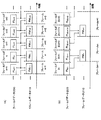
- FIG. 1 is a block diagram illustrating a configuration example of an imaging apparatus according to a first embodiment of the present invention. It is a conceptual diagram of the addition process of this imaging device.
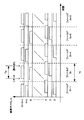
- FIG. 6 is a diagram illustrating an example of reset (electronic shutter) and readout timing of each pixel in the imaging apparatus according to the first embodiment.
- FIG. It is a figure which shows an example of the read-out address of each field of the imaging device which concerns on the 2nd Embodiment of this invention.
- the second embodiment it is a diagram showing the center of gravity of sampling at the address of the pixel of the frame data FM2n + 1.
- 3rd Embodiment it is a figure which shows the example in the case of adding 2 pixels in H1 / 4V1 / 4 thinning-out mode.
- FIG. 1 is a block diagram illustrating a configuration example of an imaging apparatus according to the first embodiment of the present invention.
- the imaging apparatus 100 includes an imaging optical system 110, a photoelectric conversion unit 120 as a pixel unit, a readout circuit 130, a sampling controller 140, and a signal processing unit 150.
- the photoelectric conversion unit 120, the readout circuit 130, the sampling controller 140, and the signal processing unit 150 may be integrated into one chip as a semiconductor element or may be divided into a plurality of chips.
- the imaging apparatus 100 has a function corresponding to at least an all-pixel mode in which signals are read from all pixels and a thinning-out mode in which signals are intermittently read while skipping rows and columns.
- the operation mode is switched by an operation mode control signal 300 input from the outside of the imaging apparatus 100.
- the imaging apparatus 100 acquires different data for each field from the photoelectric conversion unit 120, adds them, and generates and outputs frame data.
- the imaging optical system 110 includes a lens, a mechanical shutter, and the like.
- the photoelectric conversion unit 120 receives light incident through the imaging optical system 110 and generates an electrical signal corresponding to the amount of light.
- the photoelectric conversion unit 120 is constituted by, for example, a CMOS (Complementary Metal Oxide Semiconductor) image sensor.
- the photoelectric conversion unit 120 includes M ⁇ N pixels arranged in a matrix of M rows ⁇ N columns. This pixel has a photoelectric conversion element formed of a photodiode that generates charges according to the amount of incident light, for example.
- a color filter array in which color filters having different spectral transmittances are regularly arranged is arranged in front of the pixels arranged in a matrix.
- a Bayer array (see FIGS. 3 and 4 to be described later) composed of RGB color filters or a complementary color filter made up of CMYG color filters can be used.
- the reading circuit 130 reads an analog electrical signal generated by the photoelectric conversion unit 120, performs AD (Analog / Digital) conversion, and outputs it as field data 200.
- AD Analog / Digital
- the sampling controller 140 controls which pixel from among the pixels arranged in M rows ⁇ N columns is read.
- the sampling controller 140 sequentially reads signals from all pixels.
- the sampling controller 140 reads signals from different pixels by changing the reading position for each field. For example, when the reading position is changed every two fields in the V1 / 4 thinning mode for reading 1/4 of M rows, the sampling controller 140 performs the following processing. That is, in this case, the sampling controller 140 reads data from the 4x rows in the field 2a, and reads a signal from the 4x + 2 rows in the field 2a + 1.
- a and x are arbitrary integers.
- the photoelectric conversion unit 120 outputs an electrical signal to the readout circuit 130 from the pixels 121 arranged in a specific row in accordance with a signal from the sampling controller 140.
- the read circuit 130 reads an electric signal from a specific column in accordance with the control signal CTL from the sampling controller 140, performs AD conversion, and outputs it as field data 200.
- the readout circuit 130 may read electrical signals from all columns in accordance with the control signal CLT from the sampling controller 140, perform AD conversion, and output only signals in a specific column as field data 200.
- the signal processing unit 150 performs signal processing on the field data 200 output from the readout circuit 130 and outputs the processed data as frame data 210 to the outside.
- the signal processing unit 150 includes an addition processing unit 151 and a memory 152, and switches whether to add and output the field data 200 of a plurality of fields by the operation mode control signal 300.
- the operation mode control signal 300 designates the all-pixel mode
- the signal processing unit 150 performs signal processing only on the field data 200 of a single field and outputs it as frame data 210.
- the operation mode control signal 300 designates the thinning mode
- the signal processing unit 150 adds the data of a plurality of fields and outputs it as frame data 210.
- the memory 152 of the signal processing unit 150 temporarily stores the field data 200 output from the reading circuit 130. Further, in the thinning mode, the addition processing unit 151 of the signal processing unit 150 performs addition processing on the plurality of field data 200 stored in the memory 152 or output from the reading circuit 130.
- the addition processing unit 151 performs addition (or addition average) of data located at the same coordinates for all the pixels in the field data of a plurality of fields. Thus, one piece of image data is generated from a plurality of pieces of image data.
- the addition processing unit 151 adds m pieces of field data 200 to generate one piece of image data.
- the memory 152 needs to store at least m ⁇ 1 field data 200.
- the imaging apparatus 100 changes the reading position for each field in the thinning mode, and adds the field data 200 of a plurality of fields to generate the frame data 210.
- frame data for 1 to n ⁇ (m ⁇ 1) frames can be obtained from the field data 200 of n fields.
- how many frames of frame data 210 are to be obtained from the field data 200 of n fields can be freely determined from a necessary frame rate or the like.
- 2A and 2B are conceptual diagrams of addition processing of the imaging apparatus.
- FIG. 2A shows an example in which frame data 210 for (n ⁇ 1) frames is generated from field data 200 of n fields.
- Frame data FMn of frame n is generated by adding field data FLn of field n and field data FLn-1 of field n-1.
- frame data FMn + 1 of frame n + 1 is generated by adding field data FLn + 1 and FLn.
- FIG. 2B shows an example of generating frame data 210 for n frames from field data 200 of 2n fields.
- Frame data FMn of frame n is generated by adding field data FL2n and FL2n + 1.
- frame data FMn + 1 of frame n + 1 is generated by adding field data FL2 (n + 1) and FL2 (n + 1) +1.
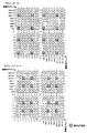
- 3A shows the read address of the 2n field
- FIG. 3B shows the read address of the 2n + 1 field.
- n is an arbitrary integer.
- 4A and 4B are examples of field data 200 when a signal is read from the pixel at the address shown in FIG.
- 4x2j rows of pixels are output to even rows 2j of field data FL2n of field 2n, and 4 (2j + 1) +1 rows of pixels are output to odd rows 2j + 1.
- Data of 4 ⁇ 2i columns of pixels is output to even columns 2i, and 4 (2i + 1) +1 columns of pixels are output to odd columns 2i + 1.
- data of 4 ⁇ 2j + 2 pixels is output to the even-numbered row 2j row of the field data FL2n + 1 of the field 2n + 1, and 4 (2j + 1) + 1-row data of the pixel is output to the odd-numbered row 2j + 1 row.
- Data of 4 ⁇ 2i + 2 columns of pixels is output in even-numbered columns 2i, and data of 4 (2i + 1) +1 columns of pixels are output in odd-numbered columns 2i + 1.
- the spatial phase shifts between even rows and odd rows, even columns and odd columns only with a single field.
- the data of 4 ⁇ 2j rows of pixels is output to the even-numbered rows 2n of the field data
- the data of 4 (2i + 1) +1 rows of pixels is output to the odd-numbered rows 2n + 1.
- the sampling center of gravity is shifted by one pixel. The same applies to the column direction. For this reason, if signal processing is performed on the premise that even-numbered and odd-numbered rows of field data have the same pitch as in the all-pixel mode, a jaggy occurs in the processed image.
- the imaging apparatus 100 the plurality of field data 200 whose read positions are changed are added, so that the centroids of the sampling of the even-numbered rows and the odd-numbered rows are equal pitches.
- FIG. 5 shows the sampling centroid of the frame data FM2n + 1 obtained by adding the field data FL2n and FL2n + 1.
- the row address of the pixels output to the even-numbered rows 2j of the field data FL2n is 4 ⁇ 2j
- the row address of the pixels output to the even-numbered rows 2j of the field data FL2n + 1 is 4 ⁇ 2j + 2. Therefore, when the even-numbered rows 2j of the field data FL2n and FL2n + 1 are added together, the center of gravity of sampling in the row direction becomes 4 ⁇ 2j + 1 of the row address of the pixel.
- the row addresses of the pixels output to odd rows 2j + 1 in both the field data FL2n and FL2n + 1 are 4x (2j + 1) +1, and the center of gravity does not change even after the addition processing.
- the center of gravity of sampling of the k-th row (k is an arbitrary integer satisfying 0 ⁇ 4k ⁇ M) of the frame data FM2n + 1 is 4k + 1 for both the even-numbered row and the odd-numbered row, and the center-of-gravity shift due to the row is eliminated.
- the column address of the pixel output to the even column 2i of the field data FL2n is 4 ⁇ 2i
- the column address of the pixel output to the even row 2i of the field data FL2n + 1 is 4 ⁇ 2i + 2. Therefore, when the even-numbered rows 2i of the field data FL2n and FL2n + 1 are added, the center of gravity of sampling in the column direction becomes 4 ⁇ 2i + 1 of the column address of the pixel.
- the column address of the pixel output to the odd-numbered row 2i + 1 column in both the field data FL2n and FL2n + 1 is 4x (2j + 1) +1, and the center of gravity does not change even after the addition processing.
- the center of gravity of sampling of the l-th column (L is an arbitrary integer satisfying 0 ⁇ 4l ⁇ N) of the frame data FM2n + 1 is 4l + 1 for both the even-numbered column and the odd-numbered column, and the center-of-gravity shift due to the column is eliminated.
- the imaging apparatus 100 generates a frame data 210 by adding a plurality of field data 200 with different readout positions in the thinning mode, so that the center of gravity of pixel sampling in each row and column is constant. Thus, jaggy can be reduced.
- the pixel readout addresses in each field may be selected so that the center of gravity of each row and column is aligned when m pieces of field data are added, and are not limited to the examples in FIGS.
- the S / N ratio of the frame data 210 is improved by adding the plurality of field data 200.
- the output values of the respective images are the same SFD in the fields 2n and 2n + 1, and the noise is NFD.
- FIG. 6 shows an example of reset (electronic shutter) and readout timing of each pixel in the imaging apparatus 100.
- the horizontal axis represents time, and the vertical axis represents pixel row addresses.
- Data is read from the row address 0 of the pixel at the head of the field 2n. Similarly, data is read from the row address 2 of the pixel at the head of the field 2n + 1.
- signals are read from the row address 4 (i + 1) +1 of the same pixel in the odd rows 2i + 1 of the fields 2n and 2n + 1. Therefore, the accumulation time Te from the reset of the electric signal of each pixel to the reading of the signal needs to be shorter than the field period Tf which is the length of one field.
- the frame data 210 is generated by adding the plurality of field data 200 whose read positions are changed in the thinning mode. This makes it possible to reduce the jaggies while keeping the sampling centroid of each row constant. Also, by adding a plurality of fields to generate frame data, the S / N ratio can be improved and the image quality can be improved.
- the entire configuration of the imaging apparatus according to the second embodiment of the present invention can employ the configuration shown in FIG.
- the imaging apparatus 100 ⁇ / b> A corresponds to at least an all-pixel mode in which signals are read from all pixels and a thinning-out mode in which signals are intermittently read while skipping rows and columns, and the operation mode can be controlled by an operation mode control signal 300.
- the point is also the same as in the first embodiment.
- the imaging apparatus 100A acquires different data for each field from the photoelectric conversion unit 120, adds them, and generates and outputs frame data.
- the imaging apparatus 100A generates frame data by adding a plurality of field data 200.
- the imaging apparatus 100A when generating frame data, the imaging apparatus 100A performs addition processing on data at the same address of field data.
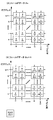
- FIG. 7 shows an example of the read address of each field of the imaging apparatus according to the second embodiment of the present invention.
- data is read from pixels located at different addresses between a plurality of fields to be added.
- the signal is read from the pixel row address 4x2j for the even-numbered row 2i row of the field data FD2n of the field 2n, and the signal is read from the pixel row address 4x2j + 3 for the odd-numbered row 2i + 1 row.
- a signal is read from the pixel row address 4x2j + 2 for the even row 2i row of the field data FD2n + 1 of the field 2n + 1, and a signal is read from the pixel row address 4x (2j + 1) +3 to the odd row 2i + 1 row.
- signals are read from pixels located at intersections of 4x2j + 2 rows and 4x (2j + 1) +3 rows, 4x2i + 2 columns and 4x (2i + 1) +1 columns.
- 4 ⁇ 2i columns of pixels are output to the even columns 2i of the field data FL2n
- 4 (2i + 1) +1 columns of pixels are output to the odd columns 2i + 1.
- the field data FL2n + 1 is output in the same manner as in the first embodiment in that data of 4 ⁇ 2i + 2 columns of pixels are output in the even column 2i row and 4 (2i + 1) +1 columns of pixels are output in the odd column 2i + 1.
- the addresses of the pixels to be read are different in all the R, G, and B pixels.
- the address of each pixel is represented as (pixel column address, pixel row address).
- the field 2n reads (4 ⁇ 2i, 4 ⁇ 2j) pixels.
- the field 2n + 1 (4 ⁇ 2i + 2, 4 ⁇ 2j + 2) pixels are read.
- the G pixel in the field 2n, (4x2i, 4x2j + 3) and (4x (2i + 1) +1, 4x2j) pixels are read.
- FIG. 8 shows the centroid of sampling at the pixel address of the frame data FM2n + 1.
- the center of gravity of even-numbered row 2i is 4 ⁇ 2i + 1 because the row address of the pixel in field 2n is 4 ⁇ 2i and the row address of the pixel in field 2n + 1 is 4 ⁇ 2i + 2.
- the row address of the pixel in the field 2n is 4x2i + 3 and the row address of the pixel in the field 2n + 1 is 4x (2i + 1) +3
- the center of gravity of the odd row 2i + 1 is 4x (2i + 1) +1. .
- the center of gravity of sampling of the k-th row (k is an arbitrary integer satisfying 0 ⁇ 4k ⁇ M) of the frame data FM2n + 1 is 4k + 1 for both the even-numbered row and the odd-numbered row, and the center-of-gravity shift due to the row is eliminated.
- the column address of the pixel output to the even column 2i of the field data FL2n is 4 ⁇ 2i
- the column address of the pixel output to the even row 2i of the field data FL2n + 1 is 4 ⁇ 2i + 2. Therefore, when the even-numbered rows 2i of the field data FL2n and FL2n + 1 are added, the center of gravity of sampling in the column direction becomes 4 ⁇ 2i + 1 of the column address of the pixel.
- the column address of the pixel output to the odd-numbered row 2i + 1 column in both the field data FL2n and FL2n + 1 is 4x (2j + 1) +1, and the center of gravity does not change even after the addition processing.
- the center of gravity of sampling of the l-th column (L is an arbitrary integer satisfying 0 ⁇ 4l ⁇ N) of the frame data FM2n + 1 is 4l + 1 for both the even-numbered column and the odd-numbered column, and the center-of-gravity shift due to the column is eliminated.
- the imaging apparatus 100 generates a frame data 210 by adding a plurality of field data 200 with different readout positions in the thinning mode, so that the center of gravity of pixel sampling in each row and column is constant. Thus, jaggy can be reduced.
- the pixel readout address in each field may be selected so that the center of gravity of each row and column is aligned when m pieces of field data are added, and is not limited to the examples in FIGS. .
- the S / N ratio of the frame data 210 can be improved.
- each pixel can accumulate signals over a plurality of fields. For example, when the readout position is changed for each m field and m pieces of field data are added to generate one frame data, assuming that the period of one field and Tf and the accumulation time of each pixel are Te, Te Can be set in a range of 0 ⁇ Te ⁇ m ⁇ Tf.
- FIG. 9 shows an example of reset (electronic shutter) and readout timing of each pixel in the second embodiment.
- the horizontal axis indicates time
- the vertical axis indicates pixel row addresses.
- Data is read from the row address 0 of the pixel at the head of the field 2n. Thereafter, the pixel located at pixel row address 0 is not read out until field 2n + 2. From the above, the pixel located at row address 0 can be reset from the beginning of field 2n to the beginning of field 2n + 2. Therefore, the accumulation time Te from the reset of the electric signal of each pixel to the reading of the signal can be set up to the field period Tf ⁇ 2. Even if the field Tf is lengthened, the maximum accumulation time can be extended, but the frame rate is lowered.
- the maximum accumulation time can be made longer than the field period Tf by reading signals from completely different pixels between the fields to be added. That is, the maximum accumulation time can be increased while keeping the frame rate constant.
- the frame data 210 is generated by adding the plurality of field data 200 whose read positions are changed. This makes it possible to reduce the jaggies while keeping the sampling centroid of each row constant. Also, by adding a plurality of fields to generate frame data, the S / N ratio can be improved and the image quality can be improved. Furthermore, the maximum accumulation time can be made longer than the field period Tf by reading out signals from completely different pixels between the fields to be added. That is, the maximum accumulation time can be increased while keeping the frame rate constant.
- the sampling controller 140 in the third embodiment controls which pixel from among the pixels arranged in M rows ⁇ N columns is read.
- the sampling controller 140 sequentially reads signals from all pixels.
- the sampling controller 140 intermittently selects pixel rows or columns and reads out signals from some pixels.
- the photoelectric conversion unit 120 outputs an electrical signal to the readout circuit 130 from the pixels 121 arranged in a specific row in accordance with the signal from the sampling controller 140.
- the read circuit 130 reads an electrical signal from a specific column in accordance with the control signal CTL from the sampling controller 140, performs AD conversion, and outputs it as field data 200.
- the readout circuit 130 may read electrical signals from all columns in accordance with a control signal from the sampling controller 140, perform AD conversion, and output only the signals in a specific column as the field data 200.
- the signal processing unit 150 performs signal processing on the field data 200 output from the readout circuit 130 and outputs the processed data as frame data 210 to the outside.
- the signal processing unit 150 includes an addition processing unit 151 and a memory 152, and switches whether to add and output a plurality of pixel data in the field data 200 according to the operation mode control signal 300.
- FIG. 10 shows an example in the case where two pixels are added in the H1 / 4V1 / 4 thinning mode in the third embodiment.
- the address of each pixel in the field data 200 (pixel column address, pixel row address) is indicated.
- the pixels of (4x2i, 4x2j) and (4x2i + 2, 4x2j + 2) are read out.
- the signal processing unit 150 adds these two pixels and outputs the result as (2i, 2j) data of the frame data 210.
- (4x2i, 4x2j + 3) and (4x2i + 2, 4x (2j + 1) +3) are added.
- (2i, 2j + 1) data of the frame data 210 is added to (4x (2i + 1) +1, 4x2j) and (4x (2i + 1) +1, 4x2j + 2), and (2i + 1, 2j) of the frame data 210 is added.
- 4x (2i + 1) +1, 4x2j + 3) and (4x (2i + 1) +1, 4x (2j + 1) +3) are added to output data (2i + 1, 2j + 1) of the frame data 210.
- the sampling centroids of the respective rows and columns of the frame data can be made uniform by adding the plurality of pixels.
- the center of gravity of sampling is (4x2i + 1, 4x2j + 1).
- the B pixel output to (2i + 1, 2j + 1) of the frame data 210 it is (4x2 (i + 1) +1, 4x2 (j + 1) +1). That is, the center of gravity of sampling of the kth row of frame data (k is an arbitrary integer satisfying 0 ⁇ 4k ⁇ M) is 4k + 1 for both even and odd rows.
- the centroid of sampling in the l-th column (L is an arbitrary integer satisfying 0 ⁇ 4l ⁇ N) is 4l + 1 in both the even-numbered column and the odd-numbered column.
- the imaging apparatus 100B in the thinning mode, the imaging apparatus 100B generates a frame data 210 by adding a plurality of pixels of the field data 200, thereby making the sampling centroid of each row and column constant. Jagi can be reduced.
- the pixel readout address in the field data may be selected so that the centers of gravity of the respective rows and columns are aligned when a plurality of pixels are added, and is not limited to the example of FIG.
- addition processing can be performed for each row. Such an addition process can be sequentially performed one line at a time. Therefore, the size of the memory 152 may be at least one line. Also in the third embodiment, similarly to the first embodiment, the frame data 210 is generated by adding a plurality of pixel data, and the S / N ratio can be improved. The accumulation time Te in the imaging apparatus 100B needs to be shorter than the field period Tf, as in the first embodiment.
- the frame data 210 is generated by adding the plurality of field data 200 whose read positions are changed in the thinning mode. This makes it possible to reduce the jaggies while keeping the sampling centroid of each row constant. Also, by adding a plurality of fields to generate frame data, the S / N ratio can be improved and the image quality can be improved. Furthermore, since the addition processing can be sequentially performed for each row, the size required for the memory 152 can be reduced to one row.
- frame data 210 is generated by adding a plurality of field data 200 with different readout positions in the thinning mode. This makes it possible to reduce the jaggies while keeping the sampling centroid of each row constant. Also, by adding a plurality of fields to generate frame data, the S / N ratio can be improved and the image quality can be improved.
- frame data 210 is generated by adding a plurality of field data 200 with different readout positions in the thinning mode. This makes it possible to reduce the jaggies while keeping the sampling centroid of each row constant. Also, by adding a plurality of fields to generate frame data, the S / N ratio can be improved and the image quality can be improved. Furthermore, the maximum accumulation time can be made longer than the field period Tf by reading signals from completely different pixels between the fields to be added. That is, the maximum accumulation time can be increased while keeping the frame rate constant.
- frame data 210 is generated by adding a plurality of field data 200 with different readout positions in the thinning mode. This makes it possible to reduce the jaggies while keeping the sampling centroid of each row constant. Also, by adding a plurality of fields to generate frame data, the S / N ratio can be improved and the image quality can be improved. Furthermore, since the addition processing can be sequentially performed for each row, the size required for the memory 152 can be reduced to one row.
Abstract
Description
たとえば、デジタルスチルカメラで動画を撮影したり、逆にカムコーダーで静止画を撮像したりするなどの機能が一般的になってきている。 In recent years, even an image sensor having a high resolution is required to capture a good image with a low resolution.
For example, functions such as taking a moving picture with a digital still camera and taking a still picture with a camcorder have become common.
さらに一部のデジタルスチルカメラや携帯電話などでは、低解像度の撮像時にフレームレートを向上させ、従来は見ることができなかった高速の動きを撮像する機能を搭載している。 In many cases, these electronic devices are provided with a viewfinder for confirming a video, but the resolution of the viewfinder is usually lower than that of an image to be captured.
In addition, some digital still cameras and mobile phones are equipped with a function to improve the frame rate during low-resolution imaging and to capture high-speed movements that could not be seen in the past.
この方法では、フレーム毎に読み出す画素を変えることで、サンプリングの位相と周波数を異ならせ、モアレを低減する。 A CMOS image sensor that improves image quality in moving image capturing in the thinning mode is described in
In this method, by changing the pixel to be read for each frame, the sampling phase and frequency are varied, and moire is reduced.
さらに、間引きモードでは、偶数行と奇数行とでサンプリングする画素の重心がずれてしまうが、特許文献1ではその点に関しては考慮されておらず、重心を補正する処理が別途必要になるという不利益がある。 However, this method has the disadvantages that different image processing is required for each frame, the calculation load is large, and the amount of memory required is also large.
Furthermore, in the thinning mode, the centroids of the pixels to be sampled are shifted between the even-numbered rows and the odd-numbered rows. However, this point is not taken into consideration in
なお、説明は以下の順序で行う。
1.第1の実施形態(撮像装置の第1の構成および機能)
2.第2の実施形態(撮像装置の第2の構成および機能)
3.第3の実施形態(撮像装置の第3の構成および機能) Hereinafter, embodiments of the present invention will be described with reference to the drawings.
The description will be given in the following order.
1. First Embodiment (First Configuration and Function of Imaging Device)
2. Second Embodiment (Second Configuration and Function of Imaging Device)
3. Third Embodiment (Third Configuration and Function of Imaging Device)
図1は、本発明の第1の実施形態に係る撮像装置の構成例を示すブロック図である。 <1. First Embodiment>
FIG. 1 is a block diagram illustrating a configuration example of an imaging apparatus according to the first embodiment of the present invention.
光電変換部120、読み出し回路130、サンプリングコントローラー140、信号処理部150は、半導体素子として1チップにまとめても良いし、複数チップに分けても良い。 The
The
動作モードは、撮像装置100の外部から入力される動作モード制御信号300によって切り替えられる。
本撮像装置100は、間引きモード時、光電変換部120からフィールド毎に異なったデータを取得し、それらを加算処理することでフレームのデータを生成して出力する。 The
The operation mode is switched by an operation
In the thinning mode, the
光電変換部120は、たとえばCMOS(Complementary Metal Oxide Semiconductor)イメージセンサなどにより構成される。
光電変換部120は、M行×N列のマトリクス状に配置されたM×N個の画素を有する。
この画素は、たとえば入射する光量に応じた電荷を発生するフォトダイオードからなる光電変換素子を有する。
マトリクス状に配置された画素の前面には、分光透過率が異なるカラーフィルターを規則的に配列したカラーフィルタアレイが配置される。
カラーフィルタアレイは、たとえばRGBのカラーフィルターで構成したベイヤー配列(後述する図3や図4等参照)やCMYGのカラーフィルターからなる補色フィルタを用いることができる。 The
The
The
This pixel has a photoelectric conversion element formed of a photodiode that generates charges according to the amount of incident light, for example.
A color filter array in which color filters having different spectral transmittances are regularly arranged is arranged in front of the pixels arranged in a matrix.
As the color filter array, for example, a Bayer array (see FIGS. 3 and 4 to be described later) composed of RGB color filters or a complementary color filter made up of CMYG color filters can be used.
サンプリングコントローラー140は、動作モード制御信号300が全画素モードを指定している場合には、全ての画素から順次信号を読み出す。
それに対して動作モード制御信号300が間引きモードを指定している場合には、サンプリングコントローラー140は、フィールド毎に読み出し位置を変えて、異なった画素から信号を読み出す。
たとえば、M行の内1/4の行を読み出すV1/4間引きモードにて2フィールド毎に読み出し位置を変える場合、サンプリングコントローラー140は、次の処理を行う。
すなわち、この場合、サンプリングコントローラー140は、フィールド2aでは4x行からデータを読み出し、フィールド2a+1では4x+2行から信号を読み出す。
ここで、a、xは任意の整数である。 In accordance with the operation
When the operation
On the other hand, when the operation
For example, when the reading position is changed every two fields in the V1 / 4 thinning mode for
That is, in this case, the
Here, a and x are arbitrary integers.
読み出し回路130は、サンプリングコントローラー140からの制御信号CTLに従い、特定の列から電気信号を読み取り、AD変換して、フィールドデータ200として出力する。
もしくは、読み出し回路130は、サンプリングコントローラー140からの制御信号CLTに従い、すべての列から電気信号を読み取り、AD変換して、特定の列の信号のみをフィールドデータ200として出力しても良い。 The
The
Alternatively, the
信号処理部150は、加算処理部151とメモリ152を有し、動作モード制御信号300によって、複数フィールドのフィールドデータ200を加算処理して出力するか否かを切り替える。
信号処理部150は、動作モード制御信号300が全画素モードを指定している場合、信号処理部は単一のフィールドのフィールドデータ200に対してのみ信号処理を行い、フレームデータ210として出力する。
これに対して、信号処理部150は、動作モード制御信号300が間引きモードを指定している場合、信号処理部は複数のフィールドのデータを加算処理して、フレームデータ210として出力する。 The
The
When the operation
On the other hand, when the operation
さらに間引きモードでは、信号処理部150の加算処理部151は、メモリ152に保存された、もしくは読み出し回路130から出力された複数のフィールドデータ200を加算処理する。 In the thinning mode, the
Further, in the thinning mode, the
読み出し位置をm(mは任意の整数)フィールド毎に変える場合、加算処理部151はm枚のフィールドデータ200を加算して1枚の画像データを生成する。
このとき、メモリ152は少なくともm-1枚分のフィールドデータ200を保存する必要がある。 Specifically, the
When the reading position is changed for each m (m is an arbitrary integer) field, the
At this time, the
本撮像装置100の加算処理では、nフィールドのフィールドデータ200から、1~n-(m-1)フレーム分のフレームデータを得ることができる。
この加算処理では、nフィールドのフィールドデータ200から、フレームデータ210を何フレーム分得るかは、必要なフレームレート等から自由に決めることができる。 Next, the addition process in the first embodiment will be described.
In the addition processing of the
In this addition processing, how many frames of
図2(A)および(B)読み出し位置を2フィールド毎に変える(m=2)場合について示している。 2A and 2B are conceptual diagrams of addition processing of the imaging apparatus.
2A and 2B show the case where the reading position is changed every two fields (m = 2).
フレームnのフレームデータFMnは、フィールドnのフィールドデータFLnとフィールドn-1のフィールドデータFLn-1を加算処理して生成されている。
同様に、フレームn+1のフレームデータFMn+1は、フィールドデータFLn+1とFLnを加算処理して生成されている。 FIG. 2A shows an example in which
Frame data FMn of frame n is generated by adding field data FLn of field n and field data FLn-1 of field n-1.
Similarly, frame data FMn + 1 of frame n + 1 is generated by adding field data FLn + 1 and FLn.
フレームnのフレームデータFMnは、フィールドデータFL2nとFL2n+1を加算処理して生成されている。
同様に、フレームn+1のフレームデータFMn+1は、フィールドデータFL2(n+1)とFL2(n+1)+1を加算処理して生成されている。 FIG. 2B shows an example of generating
Frame data FMn of frame n is generated by adding field data FL2n and FL2n + 1.
Similarly, frame data FMn + 1 of frame n + 1 is generated by adding field data FL2 (n + 1) and FL2 (n + 1) +1.
すなわち、フレームデータFM2nのX行Y列のデータをFMD2n(X,Y)は、フィールドデータFL2nのX行Y列のデータをFLD2n(X,Y)とすると、{FMD2n(X,Y)=FLD2n-1(X,Y)+FLD2n(X,Y)}となる。 When adding the field data FLn of the field n and the field data FLn-1 of the field n-1 to generate the frame data FMn of the frame n, the
That is, if FMD2n (X, Y) is the data in the X row and Y column of the frame data FM2n and FLD2n (X, Y) is the data in the X row and Y column of the field data FL2n, {FMD2n (X, Y) = FLD2n -1 (X, Y) + FLD2n (X, Y)}.
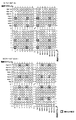
ここでは、M行の内1/4の行と、N列の中の1/4の列を読み出すH1/4V1/4間引きモードにて、2フィールド毎に読み出し位置を変える(m=2)場合を例に説明する。 Next, details of the
Here, when the reading position is changed every two fields (m = 2) in the H1 / 4V1 / 4 thinning mode for reading 1/4 of M rows and 1/4 of N columns Will be described as an example.
図3(A)は2nフィールドの、図3(B)は2n+1フィールドの読み出しアドレスをそれぞれ示している。
ここでnは任意の整数である。 FIGS. 3A and 3B show an example of the read address of each field when m = 2 in the H1 / 4 V1 / 4 thinning mode in the first embodiment.
3A shows the read address of the 2n field, and FIG. 3B shows the read address of the 2n + 1 field.
Here, n is an arbitrary integer.
ここで、i,jは、4x(2j+1)+3<M、4x(2i+1)+3<Nを満たす任意の整数である。
また、2n+1フィールドでは、4x2j+2行および4x(2j+1)+1行と、4x2i+2列および4x(2i+1)+1列の交点に位置する画素から信号を読み出している。
以上のように、本撮像装置100は、間引きモード時、フィールド毎に偶数行2j行および偶数列2i列の画素の読み出し位置を変更する。 3A and 3B, in the 2n field, 4 × 2j rows and 4x (2j + 1) +1 rows, 4 × 2i columns and 4x (2i + 1) +1 out of pixels arranged in M rows × N columns. The signal from the pixel located at the intersection of the columns is read out.
Here, i and j are arbitrary integers satisfying 4x (2j + 1) +3 <M and 4x (2i + 1) +3 <N.
In the 2n + 1 field, signals are read from pixels located at intersections of 4x2j + 2 rows and 4x (2j + 1) +1 rows, 4x2i + 2 columns and 4x (2i + 1) +1 columns.
As described above, the
偶数列2i行には画素の4x2i列、奇数列2i+1列には画素の4(2i+1)+1列のデータが出力される。 As shown in FIG. 4A, 4x2j rows of pixels are output to even
Data of 4 × 2i columns of pixels is output to even
偶数列2i行には画素の4x2i+2列、奇数列2i+1列には画素の4(2i+1)+1列のデータが出力される。 Further, as shown in FIG. 4B, data of 4 × 2j + 2 pixels is output to the even-numbered
Data of 4 × 2i + 2 columns of pixels is output in even-numbered
たとえば、フィールド2nについて見てみると、フィールドデータの偶数行2nには画素の4x2j行のデータが出力されているのに対して、奇数行2n+1には画素の4(2i+1)+1行のデータが出力されており、サンプリングの重心が1画素分ずれている。
列方向についても同様である。
そのため、全画素モードと同様にフィールドデータの偶数行と奇数行とが等ピッチであることを前提として信号処理を行ってしまうと、処理後の画像にジャギが発生してしまう。 In the
For example, when looking at the
The same applies to the column direction.
For this reason, if signal processing is performed on the premise that even-numbered and odd-numbered rows of field data have the same pitch as in the all-pixel mode, a jaggy occurs in the processed image.
よって、フィールドデータのFL2nとFL2n+1の偶数行2jを足し合わせると、行方向のサンプリングの重心が画素の行アドレスの4x2j+1になる。
一方、フィールドデータのFL2n、FL2n+1共に奇数行2j+1行に出力されている画素の行アドレスは4x(2j+1)+1であり、加算処理後も重心は変わらない。
以上から、フレームデータFM2n+1のk行目(kは0<4k<Mを満たす任意の整数)のサンプリングの重心は偶数行、奇数行共に4k+1になり、行による重心のずれが無くなる。 As described above, the row address of the pixels output to the even-numbered
Therefore, when the even-numbered
On the other hand, the row addresses of the pixels output to
From the above, the center of gravity of sampling of the k-th row (k is an arbitrary integer satisfying 0 <4k <M) of the frame data FM2n + 1 is 4k + 1 for both the even-numbered row and the odd-numbered row, and the center-of-gravity shift due to the row is eliminated.
よって、フィールドデータのFL2nとFL2n+1の偶数行2iを足し合わせると、列方向のサンプリングの重心は画素の列アドレスの4x2i+1になる。
一方、フィールドデータのFL2n、FL2n+1共に奇数行2i+1列に出力されている画素の列アドレスは4x(2j+1)+1であり、加算処理後も重心は変わらない。
以上から、フレームデータFM2n+1のl列目(Lは0<4l<Nを満たす任意の整数)のサンプリングの重心は偶数列、奇数列共に4l+1になり、列による重心のずれが無くなる。 Similarly, the column address of the pixel output to the
Therefore, when the even-numbered
On the other hand, the column address of the pixel output to the odd-numbered
From the above, the center of gravity of sampling of the l-th column (L is an arbitrary integer satisfying 0 <4l <N) of the frame data FM2n + 1 is 4l + 1 for both the even-numbered column and the odd-numbered column, and the center-of-gravity shift due to the column is eliminated.
たとえば、画素がフォトダイオードを用いて電気信号を発生しており、読み出し位置を2フィールド毎に変える(m=2)場合について説明する。
簡単にするためにフィールド2nと2n+1で各画その出力値が等しくSFDであり、ノイズがNFDであるとする。 Further, in the
For example, a case where a pixel generates an electrical signal using a photodiode and the reading position is changed every two fields (m = 2) will be described.
For the sake of simplicity, it is assumed that the output values of the respective images are the same SFD in the
ここで加算処理後の信号をSFM、ノイズをNFMとすると、SFM=2SFD、NFM=((NFD)2+(NFD)2)1/2=21/2NFD=(2SFD)1/2となる。
ここで加算処理前と後とでS/N比を比較すると、加算前のS/N比はSFD/NFD=(SFD)1/2、加算処理後のS/N比はSFM/NFM=2SFD/(2SFD)1/2=(2SFD)1/2となり、加算処理後にS/N比が21/2倍向上していることがわかる。 In general, under conditions where there is a certain amount of light, light shot noise when a photodiode performs photoelectric conversion becomes a dominant factor of noise NFD, and NFD≈ (SFD) 1/2.
Here, if the signal after the addition processing is SFM and the noise is NFM, SFM = 2SFD, NFM = ((NFD) 2+ (NFD) 2) 1/2 = 21 / 2NFD = (2SFD) 1/2.
Here, when the S / N ratio is compared before and after the addition process, the S / N ratio before the addition is SFD / NFD = (SFD) 1/2, and the S / N ratio after the addition process is SFM / NFM = 2SFD. / (2SFD) 1/2 = (2SFD) 1/2, and it can be seen that the S / N ratio is improved by 21/2 times after the addition processing.
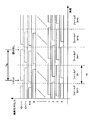
図6は、読み出し位置を2フィールド毎に変える(m=2)場合について示している。
横軸は時間、縦軸は画素の行アドレスを示している。 FIG. 6 shows an example of reset (electronic shutter) and readout timing of each pixel in the
FIG. 6 shows a case where the reading position is changed every two fields (m = 2).
The horizontal axis represents time, and the vertical axis represents pixel row addresses.
本実施形態では、フィールド2nと2n+1の奇数行2i+1行で、同じ画素の行アドレス4(i+1)+1から信号を読み出している。
そのため、各画素の電気信号をリセットしてから信号を読み出すまでの蓄積時間Teは、1フィールドの長さであるフィールド期間Tfよりも短い必要がある。 Data is read from the
In the present embodiment, signals are read from the row address 4 (i + 1) +1 of the same pixel in the
Therefore, the accumulation time Te from the reset of the electric signal of each pixel to the reading of the signal needs to be shorter than the field period Tf which is the length of one field.
これにより、各行における画素のサンプリングの重心を一定にして、ジャギを低減することができる。
また、複数フィールドを加算してフレームデータを生成することでS/N比を向上し、画質を改善することができる。 As described above, according to the
This makes it possible to reduce the jaggies while keeping the sampling centroid of each row constant.
Also, by adding a plurality of fields to generate frame data, the S / N ratio can be improved and the image quality can be improved.
本発明の第2の実施形態に係る撮像装置の全体構成は、第1の実施形態と同様、図1の構成を採用することができる。 <2. Second Embodiment>
As in the first embodiment, the entire configuration of the imaging apparatus according to the second embodiment of the present invention can employ the configuration shown in FIG.
本撮像装置100Aは、間引きモード時、光電変換部120からフィールド毎に異なったデータを取得し、それらを加算処理することでフレームのデータを生成して出力する。
第2の実施形態においても、本撮像装置100Aは、複数のフィールドデータ200を加算処理してフレームデータを生成する。
また、第1の実施形態と同様に、フレームデータを生成する際、本撮像装置100Aは、フィールドデータの同一のアドレスのデータ同士を加算処理する。 The
In the thinning mode, the
Also in the second embodiment, the
As in the first embodiment, when generating frame data, the
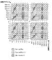
図7は、M行の内1/4の行と、N列の中の1/4の列を読み出すH1/4V1/4間引きモードにて、2フィールド毎に読み出し位置を変える(m=2)場合の例を示している。 FIG. 7 shows an example of the read address of each field of the imaging apparatus according to the second embodiment of the present invention.
FIG. 7 shows that the reading position is changed every two fields in the H1 / 4 V1 / 4 thinning mode for reading 1/4 of M rows and 1/4 of N columns (m = 2). An example of the case is shown.
図7の例では、フィールド2nのフィールドデータFD2nの偶数行2i行に対しては画素の行アドレス4x2jから信号を読み出し、奇数行2i+1行に対しては画素の行アドレス4x2j+3から信号を読み出している。
一方、フィールド2n+1のフィールドデータFD2n+1の偶数行2i行に対しては画素の行アドレス4x2j+2から信号を読み出し、奇数行2i+1行には画素の行アドレス4x(2j+1)+3から信号を読み出している。
M行×N列に配置された画素の中から、4x2j行および4x2j+3行と、4x2i列および4x(2i+1)+1列の交点に位置する画素からの信号を読み出している。
ここで、i,jは、4x(2j+1)+3<M、4x(2i+1)+3<Nを満たす任意の整数である。 In the
In the example of FIG. 7, the signal is read from the pixel row address 4x2j for the even-numbered
On the other hand, a signal is read from the pixel row address 4x2j + 2 for the
From the pixels arranged in M rows × N columns, signals from pixels located at the intersections of 4 × 2j rows and 4 × 2j + 3 rows and 4 × 2i columns and 4x (2i + 1) +1 columns are read out.
Here, i and j are arbitrary integers satisfying 4x (2j + 1) +3 <M and 4x (2i + 1) +3 <N.
ここで、フィールドデータFL2nの偶数列2i行には画素の4x2i列、奇数列2i+1列には画素の4(2i+1)+1列のデータが出力される。
そして、フィールドデータFL2n+1の偶数列2i行には画素の4x2i+2列、奇数列2i+1列には画素の4(2i+1)+1列のデータが出力される点は、第1の実施形態と同様である。 In the 2n + 1 field, signals are read from pixels located at intersections of 4x2j + 2 rows and 4x (2j + 1) +3 rows, 4x2i + 2 columns and 4x (2i + 1) +1 columns.
Here, 4 × 2i columns of pixels are output to the
The field data FL2n + 1 is output in the same manner as in the first embodiment in that data of 4 × 2i + 2 columns of pixels are output in the
各画素のアドレスを(画素の列アドレス、画素の行アドレス)と示すことにする。
R画素について見てみると、フィールド2nでは(4x2i、4x2j)の画素を読んでいる。これに対して、フィールド2n+1では(4x2i+2、4x2j+2)の画素を読んでいる。
G画素では、フィールド2nでは(4x2i、4x2j+3)および(4x(2i+1)+1、4x2j)の画素を読んでいる。これに対して、フィールド2n+1では(4x2i+2、4x(2j+1)+3)および(4x(2i+1)+1、4x2j+2)の画素を読んでいる。
さらにB画素では、フィールド2nでは(4x(2i+1)+1、4x2j+3)の画素を読んでいる。これに対して、フィールド2n+1では(4x(2i+1)+1、4x(2j+1)+3)の画素を読んでいる。 As a result, in the
The address of each pixel is represented as (pixel column address, pixel row address).
Looking at the R pixel, the
In the G pixel, in the
Further, in the B pixel, (4x (2i + 1) +1, 4x2j + 3) pixels are read in the
一方、奇数行2i+1行の重心は、フィールド2nの画素の行アドレスが4x2i+3、フィールド2n+1の画素の行アドレスが4x(2i+1)+3であることから、画素の行アドレスの4x(2i+1)+1になる。
以上から、フレームデータFM2n+1のk行目(kは0<4k<Mを満たす任意の整数)のサンプリングの重心は偶数行、奇数行共に4k+1になり、行による重心のずれが無くなる。 In FIG. 8, the center of gravity of even-numbered
On the other hand, since the row address of the pixel in the
From the above, the center of gravity of sampling of the k-th row (k is an arbitrary integer satisfying 0 <4k <M) of the frame data FM2n + 1 is 4k + 1 for both the even-numbered row and the odd-numbered row, and the center-of-gravity shift due to the row is eliminated.
よって、フィールドデータのFL2nとFL2n+1の偶数行2iを足し合わせると、列方向のサンプリングの重心は画素の列アドレスの4x2i+1になる。
一方、フィールドデータのFL2n、FL2n+1共に奇数行2i+1列に出力されている画素の列アドレスは4x(2j+1)+1であり、加算処理後も重心は変わらない。
以上から、フレームデータFM2n+1のl列目(Lは0<4l<Nを満たす任意の整数)のサンプリングの重心は偶数列、奇数列共に4l+1になり、列による重心のずれが無くなる。 Similarly, the column address of the pixel output to the
Therefore, when the even-numbered
On the other hand, the column address of the pixel output to the odd-numbered
From the above, the center of gravity of sampling of the l-th column (L is an arbitrary integer satisfying 0 <4l <N) of the frame data FM2n + 1 is 4l + 1 for both the even-numbered column and the odd-numbered column, and the center-of-gravity shift due to the column is eliminated.
なお、各フィールドにおける画素の読み出しアドレスは、m枚のフィールドデータを加算したときに、各行、列の重心が揃う様に選択すればよく、図3から図5の例に限定されるものではない。 As described above, the
The pixel readout address in each field may be selected so that the center of gravity of each row and column is aligned when m pieces of field data are added, and is not limited to the examples in FIGS. .
第2の実施形態では、加算する複数のフィールド間で異なった画素から信号を読み出す。そのため各画素では、複数のフィールドにまたがって信号を蓄積することができる。
たとえば、mフィールド毎に読み出し位置を変え、m個のフィールドデータを加算処理して1枚のフレームデータを生成する場合、1つのフィールドの期間とTf、各画素の蓄積時間をTeとすると、Teは0<Te<m×Tfの範囲に設定することができる。 Next, the accumulation time of each pixel in the second embodiment will be described.
In the second embodiment, signals are read from different pixels between a plurality of fields to be added. Therefore, each pixel can accumulate signals over a plurality of fields.
For example, when the readout position is changed for each m field and m pieces of field data are added to generate one frame data, assuming that the period of one field and Tf and the accumulation time of each pixel are Te, Te Can be set in a range of 0 <Te <m × Tf.
図9は、読み出し位置を2フィールド毎に変える(m=2)場合について示している。
図9において、横軸は時間、縦軸は画素の行アドレスを示している。 FIG. 9 shows an example of reset (electronic shutter) and readout timing of each pixel in the second embodiment.
FIG. 9 shows a case where the reading position is changed every two fields (m = 2).
In FIG. 9, the horizontal axis indicates time, and the vertical axis indicates pixel row addresses.
以上から、行アドレス0に位置する画素のリセットは、フィールド2nの先頭から、フィールド2n+2の先頭で行うことができる。
そのため、各画素の電気信号をリセットしてから信号を読み出すまでの蓄積時間Teは、最大でフィールド期間Tf×2まで設定することができる。
フィールドTfを長くすることでも最大の蓄積時間を伸ばすことはできるが、フレームレートが低下してしまう。 Data is read from the
From the above, the pixel located at
Therefore, the accumulation time Te from the reset of the electric signal of each pixel to the reading of the signal can be set up to the field period Tf × 2.
Even if the field Tf is lengthened, the maximum accumulation time can be extended, but the frame rate is lowered.
すなわち、フレームレートを一定に保ったまま、最大の蓄積時間を増やすことができる。 On the other hand, as described above, the maximum accumulation time can be made longer than the field period Tf by reading signals from completely different pixels between the fields to be added.
That is, the maximum accumulation time can be increased while keeping the frame rate constant.
これにより、各行における画素のサンプリングの重心を一定にして、ジャギを低減することができる。
また、複数フィールドを加算してフレームデータを生成することでS/N比を向上し、画質を改善することができる。
さらに、加算処理を行うフィールド間で完全に異なった画素から信号を読み出すことで、最大の蓄積時間をフィールド期間Tfより長くすることができる。すなわち、フレームレートを一定に保ったまま、最大の蓄積時間を増やすことができる。 As described above, according to the imaging apparatus of the second embodiment, in the thinning mode, the
This makes it possible to reduce the jaggies while keeping the sampling centroid of each row constant.
Also, by adding a plurality of fields to generate frame data, the S / N ratio can be improved and the image quality can be improved.
Furthermore, the maximum accumulation time can be made longer than the field period Tf by reading out signals from completely different pixels between the fields to be added. That is, the maximum accumulation time can be increased while keeping the frame rate constant.
次に、本発明の第3の実施形態について説明する。
第3の実施形態では、間引きモード時に、フィールドデータの中の同色の複数の画素データを加算して重心を揃え、フレームデータを作成する。
本発明の第3の実施形態に係る撮像装置の全体構成は、第1の実施形態と同様、図1の構成を取ることができる。 <3. Third Embodiment>
Next, a third embodiment of the present invention will be described.
In the third embodiment, in the thinning mode, a plurality of pixel data of the same color in the field data are added to align the center of gravity, and frame data is created.
The overall configuration of an imaging apparatus according to the third embodiment of the present invention can take the configuration shown in FIG. 1 as in the first embodiment.
サンプリングコントローラー140は、動作モード制御信号300が全画素モードを指定している場合には、全ての画素から順次信号を読み出す。
これに対して、サンプリングコントローラー140は、動作モード制御信号300が間引きモードを指定している場合には、画素の行または列を間欠的に選択し、一部の画素から信号を読み出す。 In accordance with the operation
When the operation
On the other hand, when the operation
また、読み出し回路130は、第1の実施形態と同様、サンプリングコントローラー140からの制御信号CTLに従い、特定の列から電気信号を読み取り、AD変換して、フィールドデータ200として出力する。
もしくは、読み出し回路130は、サンプリングコントローラー140からの制御信号に従い、すべての列から電気信号を読み取り、AD変換して、特定の列の信号のみをフィールドデータ200として出力しても良い。 As in the first embodiment, the
In addition, as in the first embodiment, the
Alternatively, the
信号処理部150は、加算処理部151とメモリ152を有し、動作モード制御信号300によって、フィールドデータ200の中の複数の画素データを加算処理して出力するか否かを切り替える。 The
The
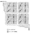
図10は、第3の実施形態において、H1/4V1/4間引きモードにて、2画素を加算処理する場合の例を示している。
ここで、フィールドデータ200の各画素のアドレスを(画素の列アドレス、画素の行アドレス)示すことにする。 Next, details of the
FIG. 10 shows an example in the case where two pixels are added in the H1 / 4V1 / 4 thinning mode in the third embodiment.
Here, the address of each pixel in the field data 200 (pixel column address, pixel row address) is indicated.
信号処理部150では、この2つの画素を加算処理し、フレームデータ210の(2i、2j)のデータとして出力する。
さらにG画素では、(4x2i、4x2j+3)と(4x2i+2、4x(2j+1)+3)とを加算処理する。そして、フレームデータ210の(2i、2j+1)のデータを、(4x(2i+1)+1、4x2j)と(4x(2i+1)+1、4x2j+2)とを加算処理して、フレームデータ210の(2i+1、2j)のデータを出力する。
また、B画素では、4x(2i+1)+1、4x2j+3)と(4x(2i+1)+1、4x(2j+1)+3)とを加算して、フレームデータ210の(2i+1、2j+1)のデータを出力する。 Looking at the R pixel in the example of FIG. 10, the pixels of (4x2i, 4x2j) and (4x2i + 2, 4x2j + 2) are read out.
The
Further, in the G pixel, (4x2i, 4x2j + 3) and (4x2i + 2, 4x (2j + 1) +3) are added. Then, (2i, 2j + 1) data of the
In the B pixel, 4x (2i + 1) +1, 4x2j + 3) and (4x (2i + 1) +1, 4x (2j + 1) +3) are added to output data (2i + 1, 2j + 1) of the
たとえば、フレームデータ210の(2i、2j)に出力されるR画素では、サンプリングの重心は(4x2i+1、4x2j+1)になっている。
また、フレームデータ210の(2i+1、2j+1)に出力されるB画素では、(4x2(i+1)+1、4x2(j+1)+1)になっている。
すなわち、フレームデータのk行目(kは0<4k<Mを満たす任意の整数)のサンプリングの重心は偶数行、奇数行共に4k+1になる。l列目(Lは0<4l<Nを満たす任意の整数)のサンプリングの重心は偶数列、奇数列共に4l+1になり、行、列による重心のずれが無くなる。 As described above, the sampling centroids of the respective rows and columns of the frame data can be made uniform by adding the plurality of pixels.
For example, in the R pixel output to (2i, 2j) of the
In the B pixel output to (2i + 1, 2j + 1) of the
That is, the center of gravity of sampling of the kth row of frame data (k is an arbitrary integer satisfying 0 <4k <M) is 4k + 1 for both even and odd rows. The centroid of sampling in the l-th column (L is an arbitrary integer satisfying 0 <4l <N) is 4l + 1 in both the even-numbered column and the odd-numbered column.
なお、フィールドデータにおける画素の読み出しアドレスは、複数の画素を加算した時に、各行、列の重心が揃う様に選択すればよく、図10の例に限定されるものではない。 As described above, in the thinning mode, the
Note that the pixel readout address in the field data may be selected so that the centers of gravity of the respective rows and columns are aligned when a plurality of pixels are added, and is not limited to the example of FIG.
また、第3の実施形態においても第1の実施形態と同様、複数の画素データを加算処理してフレームデータ210を生成しておりS/N比を向上することができる。
本撮像装置100Bにおける、蓄積時間Teは、第1の実施形態同様、フィールド期間Tfよりも短い必要がある。 As described above, in the third embodiment of the present invention, addition processing can be performed for each row. Such an addition process can be sequentially performed one line at a time. Therefore, the size of the
Also in the third embodiment, similarly to the first embodiment, the
The accumulation time Te in the
これにより、各行における画素のサンプリングの重心を一定にして、ジャギを低減することができる。
また、複数フィールドを加算してフレームデータを生成することでS/N比を向上し、画質を改善することができる。
さらに行毎に順次加算処理を行うことができるので、メモリ152に必要とされるサイズが1行分と小さくすることができる。 As described above, according to the
This makes it possible to reduce the jaggies while keeping the sampling centroid of each row constant.
Also, by adding a plurality of fields to generate frame data, the S / N ratio can be improved and the image quality can be improved.
Furthermore, since the addition processing can be sequentially performed for each row, the size required for the
本願発明の第1の実施形態における撮像装置によれば、間引きモード時に、読み出し位置を変えた複数のフィールドデータ200を加算処理してフレームデータ210を生成する。
これにより、各行における画素のサンプリングの重心を一定にして、ジャギを低減することができる。
また、複数フィールドを加算してフレームデータを生成することでS/N比を向上し、画質を改善することができる。 As described above, according to the first embodiment, the second embodiment, and the third embodiment, the following effects can be obtained.
According to the imaging apparatus of the first embodiment of the present invention,
This makes it possible to reduce the jaggies while keeping the sampling centroid of each row constant.
Also, by adding a plurality of fields to generate frame data, the S / N ratio can be improved and the image quality can be improved.
これにより、各行における画素のサンプリングの重心を一定にして、ジャギを低減することができる。
また、複数フィールドを加算してフレームデータを生成することでS/N比を向上し、画質を改善することができる。
さらに加算処理を行うフィールド間で完全に異なった画素から信号を読み出すことで、最大の蓄積時間をフィールド期間Tfより長くすることができる。
すなわち、フレームレートを一定に保ったまま、最大の蓄積時間を増やすことができる。 In addition, according to the imaging apparatus of the second embodiment of the present invention,
This makes it possible to reduce the jaggies while keeping the sampling centroid of each row constant.
Also, by adding a plurality of fields to generate frame data, the S / N ratio can be improved and the image quality can be improved.
Furthermore, the maximum accumulation time can be made longer than the field period Tf by reading signals from completely different pixels between the fields to be added.
That is, the maximum accumulation time can be increased while keeping the frame rate constant.
これにより、各行における画素のサンプリングの重心を一定にして、ジャギを低減することができる。
また、複数フィールドを加算してフレームデータを生成することでS/N比を向上し、画質を改善することができる。
さらに行毎に順次加算処理を行うことができるので、メモリ152に必要とされるサイズが1行分と小さくすることができる。 Furthermore, according to the imaging apparatus of the third embodiment of the present invention,
This makes it possible to reduce the jaggies while keeping the sampling centroid of each row constant.
Also, by adding a plurality of fields to generate frame data, the S / N ratio can be improved and the image quality can be improved.
Furthermore, since the addition processing can be sequentially performed for each row, the size required for the
Claims (7)
- 複数の画素がマトリクス状に配列された画素部と、
上記画素部で発生したアナログ信号を変換処理してフィールドデータとして出力する読み出し回路と、
動作モード制御信号に応じて上記画素部のいずれの画素から信号を読み出すかを制御するコントローラーと、
上記読み出し回路から出力されるフィールドデータに対して信号処理を行い、フレームデータとして出力する信号処理部と、を有し、
上記コントローラーは、
上記動作モード制御信号が全画素モードを指定している場合には、全ての画素から順次信号を読み出し、
上記動作モード制御信号が間引きモードを指定している場合には、フィールド毎に読み出し位置を変えて、異なった画素から信号を読み出すように制御し、
上記信号処理部は、
上記動作モード制御信号が全画素モードを指定している場合、単一のフィールドのフィールドデータに対して信号処理を行ってフレームデータとして出力し、
上記動作モード制御信号が間引きモードを指定している場合、複数のフィールドのデータを加算処理して、フレームデータとして出力する
撮像装置。 A pixel portion in which a plurality of pixels are arranged in a matrix;
A readout circuit that converts the analog signal generated in the pixel portion and outputs it as field data;
A controller that controls which pixel of the pixel unit reads the signal in accordance with the operation mode control signal;
A signal processing unit that performs signal processing on the field data output from the readout circuit and outputs the data as frame data;
The above controller
When the operation mode control signal specifies the all-pixel mode, signals are sequentially read from all the pixels,
When the operation mode control signal specifies the thinning mode, the readout position is changed for each field, and control is performed so that signals are read from different pixels,
The signal processor is
When the operation mode control signal specifies all pixel mode, signal processing is performed on field data of a single field and output as frame data.
When the operation mode control signal designates a thinning mode, an imaging device that adds data of a plurality of fields and outputs the result as frame data. - 上記信号処理部は、
複数フィールドのフィールドデータにおいて、同じ座標に位置するデータの加算もしくは加算平均を全ての画素について行うことによって、複数の画像データから1枚の画像データを生成する
請求項1記載の撮像装置。 The signal processor is
The imaging apparatus according to claim 1, wherein one field of image data is generated from the plurality of image data by performing addition or addition averaging of data located at the same coordinates in field data of a plurality of fields for all pixels. - 上記信号処理部は、
上記動作モード制御信号が間引きモードを指定している場合において、読み出し位置をm(mは任意の整数)フィールド毎に変える場合、m枚のフィールドデータを加算して1枚の画像データを生成する
請求項1記載の撮像装置。 The signal processor is
When the operation mode control signal specifies the thinning mode, when the reading position is changed for each m (m is an arbitrary integer) field, m field data are added to generate one image data. The imaging device according to claim 1. - 上記信号処理部は、
上記動作モード制御信号が間引きモードを指定している場合、各行、列のサンプリング重心が揃うように、複数のフィールドのデータの加算処理を行う
請求項1記載の撮像装置。 The signal processor is
The imaging apparatus according to claim 1, wherein when the operation mode control signal designates a thinning mode, addition processing of data of a plurality of fields is performed so that sampling centroids of each row and column are aligned. - 各フィールドにおける画素の読み出しアドレスは、複数枚のフィールドデータを加算したときに、各行、列のサンプリング重心が揃うように選択されている
請求項1記載の撮像装置。 The imaging apparatus according to claim 1, wherein pixel readout addresses in each field are selected such that sampling centroids of each row and column are aligned when a plurality of field data are added. - 上記コントローラーは、
上記信号処理部で加算する複数のフィールド間で、別のアドレスに位置する画素からデータを読み出すように制御する
請求項1記載の撮像装置。 The above controller
The imaging apparatus according to claim 1, wherein control is performed so that data is read from a pixel located at another address between a plurality of fields added by the signal processing unit. - 上記信号処理部は、
記動作モード制御信号が間引きモードを指定している場合において、フィールドデータの中の複数の画素データを加算する処理を行うことにより、各行、列のサンプリング重心を揃える
請求項1記載の撮像装置。
The signal processor is
The imaging apparatus according to claim 1, wherein when the operation mode control signal designates the thinning mode, the sampling centroids of each row and column are aligned by performing a process of adding a plurality of pixel data in the field data.
Priority Applications (3)
| Application Number | Priority Date | Filing Date | Title |
|---|---|---|---|
| CN2010800525495A CN102612835A (en) | 2009-09-28 | 2010-09-14 | Imaging device |
| EP10818715.4A EP2485476A4 (en) | 2009-09-28 | 2010-09-14 | Imaging device |
| US13/497,373 US8830352B2 (en) | 2009-09-28 | 2010-09-14 | Image pickup device |
Applications Claiming Priority (2)
| Application Number | Priority Date | Filing Date | Title |
|---|---|---|---|
| JP2009223476A JP5625298B2 (en) | 2009-09-28 | 2009-09-28 | Imaging device |
| JP2009-223476 | 2009-09-28 |
Publications (1)
| Publication Number | Publication Date |
|---|---|
| WO2011037040A1 true WO2011037040A1 (en) | 2011-03-31 |
Family
ID=43795791
Family Applications (1)
| Application Number | Title | Priority Date | Filing Date |
|---|---|---|---|
| PCT/JP2010/065811 WO2011037040A1 (en) | 2009-09-28 | 2010-09-14 | Imaging device |
Country Status (7)
| Country | Link |
|---|---|
| US (1) | US8830352B2 (en) |
| EP (1) | EP2485476A4 (en) |
| JP (1) | JP5625298B2 (en) |
| KR (1) | KR20120074278A (en) |
| CN (1) | CN102612835A (en) |
| TW (1) | TW201138448A (en) |
| WO (1) | WO2011037040A1 (en) |
Families Citing this family (4)
| Publication number | Priority date | Publication date | Assignee | Title |
|---|---|---|---|---|
| JP5578915B2 (en) * | 2010-04-01 | 2014-08-27 | キヤノン株式会社 | Solid-state imaging device and driving method thereof |
| JP2012175600A (en) | 2011-02-24 | 2012-09-10 | Sony Corp | Imaging apparatus, imaging apparatus control method, and program |
| EP2940992A4 (en) * | 2012-12-25 | 2016-06-08 | Sony Corp | Solid state image-sensing element, method of driving same, and electronic device |
| KR20220058975A (en) * | 2016-09-16 | 2022-05-10 | 소니 세미컨덕터 솔루션즈 가부시키가이샤 | Image pickup device and electronic apparatus |
Citations (6)
| Publication number | Priority date | Publication date | Assignee | Title |
|---|---|---|---|---|
| JP2001145025A (en) * | 1999-11-12 | 2001-05-25 | Nec Corp | Solid-state image pickup device and its drive method |
| JP2003338933A (en) | 2002-05-20 | 2003-11-28 | Canon Inc | Image control equipment and its control method |
| JP2007104450A (en) * | 2005-10-06 | 2007-04-19 | Nippon Hoso Kyokai <Nhk> | Solid-state image pickup device, its device, its driving method, and signal processor |
| JP2007295230A (en) * | 2006-04-25 | 2007-11-08 | Matsushita Electric Ind Co Ltd | Solid state imaging apparatus, driving method thereof, and camera |
| JP2009088940A (en) * | 2007-09-28 | 2009-04-23 | Canon Inc | Imaging apparatus and driving method thereof |
| JP2009130580A (en) * | 2007-11-22 | 2009-06-11 | Nikon Corp | Imaging element and imaging apparatus |
Family Cites Families (10)
| Publication number | Priority date | Publication date | Assignee | Title |
|---|---|---|---|---|
| US5493335A (en) * | 1993-06-30 | 1996-02-20 | Eastman Kodak Company | Single sensor color camera with user selectable image record size |
| JP2000134549A (en) * | 1998-10-22 | 2000-05-12 | Toshiba Corp | Solid-state image pickup device |
| JP4142340B2 (en) * | 2002-05-22 | 2008-09-03 | オリンパス株式会社 | Imaging device |
| JP4190805B2 (en) * | 2002-06-12 | 2008-12-03 | オリンパス株式会社 | Imaging device |
| JP2004266369A (en) * | 2003-02-21 | 2004-09-24 | Sony Corp | Solid-state image pickup unit and its driving method |
| JP3960965B2 (en) * | 2003-12-08 | 2007-08-15 | オリンパス株式会社 | Image interpolation apparatus and image interpolation method |
| JP4416753B2 (en) * | 2006-03-31 | 2010-02-17 | キヤノン株式会社 | Solid-state imaging device |
| JPWO2008053791A1 (en) * | 2006-10-31 | 2010-02-25 | 三洋電機株式会社 | Imaging apparatus and video signal generation method in imaging apparatus |
| JP5053654B2 (en) * | 2007-02-09 | 2012-10-17 | オリンパスイメージング株式会社 | Image processing apparatus and method and electronic camera |
| JP5256725B2 (en) * | 2007-12-25 | 2013-08-07 | 株式会社ニコン | Imaging device |
-
2009
- 2009-09-28 JP JP2009223476A patent/JP5625298B2/en not_active Expired - Fee Related
-
2010
- 2010-09-14 WO PCT/JP2010/065811 patent/WO2011037040A1/en active Application Filing
- 2010-09-14 CN CN2010800525495A patent/CN102612835A/en active Pending
- 2010-09-14 EP EP10818715.4A patent/EP2485476A4/en not_active Withdrawn
- 2010-09-14 KR KR1020127007069A patent/KR20120074278A/en not_active Application Discontinuation
- 2010-09-14 US US13/497,373 patent/US8830352B2/en not_active Expired - Fee Related
- 2010-09-21 TW TW099132092A patent/TW201138448A/en unknown
Patent Citations (6)
| Publication number | Priority date | Publication date | Assignee | Title |
|---|---|---|---|---|
| JP2001145025A (en) * | 1999-11-12 | 2001-05-25 | Nec Corp | Solid-state image pickup device and its drive method |
| JP2003338933A (en) | 2002-05-20 | 2003-11-28 | Canon Inc | Image control equipment and its control method |
| JP2007104450A (en) * | 2005-10-06 | 2007-04-19 | Nippon Hoso Kyokai <Nhk> | Solid-state image pickup device, its device, its driving method, and signal processor |
| JP2007295230A (en) * | 2006-04-25 | 2007-11-08 | Matsushita Electric Ind Co Ltd | Solid state imaging apparatus, driving method thereof, and camera |
| JP2009088940A (en) * | 2007-09-28 | 2009-04-23 | Canon Inc | Imaging apparatus and driving method thereof |
| JP2009130580A (en) * | 2007-11-22 | 2009-06-11 | Nikon Corp | Imaging element and imaging apparatus |
Non-Patent Citations (1)
| Title |
|---|
| See also references of EP2485476A4 |
Also Published As
| Publication number | Publication date |
|---|---|
| US8830352B2 (en) | 2014-09-09 |
| TW201138448A (en) | 2011-11-01 |
| CN102612835A (en) | 2012-07-25 |
| EP2485476A1 (en) | 2012-08-08 |
| JP2011071927A (en) | 2011-04-07 |
| KR20120074278A (en) | 2012-07-05 |
| EP2485476A4 (en) | 2014-10-01 |
| JP5625298B2 (en) | 2014-11-19 |
| US20130016238A1 (en) | 2013-01-17 |
Similar Documents
| Publication | Publication Date | Title |
|---|---|---|
| JP5342969B2 (en) | Imaging apparatus and imaging method | |
| JP4582198B2 (en) | Solid-state imaging device, imaging device, and driving method of solid-state imaging device | |
| US8988593B2 (en) | Image sensor and image capturing apparatus with focus detection pixels | |
| US8704926B2 (en) | CMOS image sensor with selectable hard-wired binning | |
| JP2009027488A (en) | Imaging circuit and imaging device | |
| JP2007129581A (en) | Image pickup device and image pickup system | |
| JP2008278453A (en) | Image sensing apparatus and image capturing system | |
| US7457486B2 (en) | Imaging device | |
| JP5625298B2 (en) | Imaging device | |
| JP3967853B2 (en) | Solid-state imaging device and signal readout method | |
| US20150036033A1 (en) | Solid-state imaging device | |
| JP2006020037A (en) | Physical information acquisition method, physical information acquisition device, and semiconductor device for detecting physical quantity distribution | |
| US9407822B2 (en) | Image capturing apparatus capable of reducing time taken to display image on display and method of controlling the same | |
| JP5633518B2 (en) | Data processing device | |
| JP2007135073A (en) | Solid state imaging device | |
| JP3967500B2 (en) | Solid-state imaging device and signal readout method | |
| JP4984517B2 (en) | Imaging unit and imaging apparatus | |
| JP2018207502A (en) | Imaging element and imaging device | |
| JP5511205B2 (en) | Imaging apparatus and imaging method | |
| JP4333371B2 (en) | Imaging device and imaging device | |
| JP2692486B2 (en) | Solid-state imaging device | |
| JP2015156556A (en) | Solid-state image sensor | |
| JP2005260411A (en) | High sensitivity imaging apparatus | |
| JP2003101889A (en) | Electronic camera | |
| WO2013051190A1 (en) | Solid-state imaging device and electronic information device |
Legal Events
| Date | Code | Title | Description |
|---|---|---|---|
| WWE | Wipo information: entry into national phase |
Ref document number: 201080052549.5 Country of ref document: CN |
|
| 121 | Ep: the epo has been informed by wipo that ep was designated in this application |
Ref document number: 10818715 Country of ref document: EP Kind code of ref document: A1 |
|
| ENP | Entry into the national phase |
Ref document number: 20127007069 Country of ref document: KR Kind code of ref document: A |
|
| WWE | Wipo information: entry into national phase |
Ref document number: 2010818715 Country of ref document: EP |
|
| NENP | Non-entry into the national phase |
Ref country code: DE |
|
| WWE | Wipo information: entry into national phase |
Ref document number: 13497373 Country of ref document: US |