US8830352B2 - Image pickup device - Google Patents
Image pickup device Download PDFInfo
- Publication number
- US8830352B2 US8830352B2 US13/497,373 US201013497373A US8830352B2 US 8830352 B2 US8830352 B2 US 8830352B2 US 201013497373 A US201013497373 A US 201013497373A US 8830352 B2 US8830352 B2 US 8830352B2
- Authority
- US
- United States
- Prior art keywords
- data
- field
- pixel
- readout
- pixels
- Prior art date
- Legal status (The legal status is an assumption and is not a legal conclusion. Google has not performed a legal analysis and makes no representation as to the accuracy of the status listed.)
- Expired - Fee Related, expires
Links
Images


Classifications
-
- H04N9/045—
-
- H—ELECTRICITY
- H04—ELECTRIC COMMUNICATION TECHNIQUE
- H04N—PICTORIAL COMMUNICATION, e.g. TELEVISION
- H04N25/00—Circuitry of solid-state image sensors [SSIS]; Control thereof
-
- H—ELECTRICITY
- H04—ELECTRIC COMMUNICATION TECHNIQUE
- H04N—PICTORIAL COMMUNICATION, e.g. TELEVISION
- H04N25/00—Circuitry of solid-state image sensors [SSIS]; Control thereof
- H04N25/40—Extracting pixel data from image sensors by controlling scanning circuits, e.g. by modifying the number of pixels sampled or to be sampled
- H04N25/42—Extracting pixel data from image sensors by controlling scanning circuits, e.g. by modifying the number of pixels sampled or to be sampled by switching between different modes of operation using different resolutions or aspect ratios, e.g. switching between interlaced and non-interlaced mode
-
- H—ELECTRICITY
- H04—ELECTRIC COMMUNICATION TECHNIQUE
- H04N—PICTORIAL COMMUNICATION, e.g. TELEVISION
- H04N25/00—Circuitry of solid-state image sensors [SSIS]; Control thereof
- H04N25/10—Circuitry of solid-state image sensors [SSIS]; Control thereof for transforming different wavelengths into image signals
- H04N25/11—Arrangement of colour filter arrays [CFA]; Filter mosaics
- H04N25/13—Arrangement of colour filter arrays [CFA]; Filter mosaics characterised by the spectral characteristics of the filter elements
- H04N25/134—Arrangement of colour filter arrays [CFA]; Filter mosaics characterised by the spectral characteristics of the filter elements based on three different wavelength filter elements
-
- H—ELECTRICITY
- H04—ELECTRIC COMMUNICATION TECHNIQUE
- H04N—PICTORIAL COMMUNICATION, e.g. TELEVISION
- H04N25/00—Circuitry of solid-state image sensors [SSIS]; Control thereof
- H04N25/40—Extracting pixel data from image sensors by controlling scanning circuits, e.g. by modifying the number of pixels sampled or to be sampled
- H04N25/44—Extracting pixel data from image sensors by controlling scanning circuits, e.g. by modifying the number of pixels sampled or to be sampled by partially reading an SSIS array
- H04N25/445—Extracting pixel data from image sensors by controlling scanning circuits, e.g. by modifying the number of pixels sampled or to be sampled by partially reading an SSIS array by skipping some contiguous pixels within the read portion of the array
-
- H—ELECTRICITY
- H04—ELECTRIC COMMUNICATION TECHNIQUE
- H04N—PICTORIAL COMMUNICATION, e.g. TELEVISION
- H04N25/00—Circuitry of solid-state image sensors [SSIS]; Control thereof
- H04N25/40—Extracting pixel data from image sensors by controlling scanning circuits, e.g. by modifying the number of pixels sampled or to be sampled
- H04N25/44—Extracting pixel data from image sensors by controlling scanning circuits, e.g. by modifying the number of pixels sampled or to be sampled by partially reading an SSIS array
- H04N25/447—Extracting pixel data from image sensors by controlling scanning circuits, e.g. by modifying the number of pixels sampled or to be sampled by partially reading an SSIS array by preserving the colour pattern with or without loss of information
-
- H04N5/343—
-
- H04N5/3456—
-
- H04N5/3458—
-
- H—ELECTRICITY
- H04—ELECTRIC COMMUNICATION TECHNIQUE
- H04N—PICTORIAL COMMUNICATION, e.g. TELEVISION
- H04N25/00—Circuitry of solid-state image sensors [SSIS]; Control thereof
- H04N25/10—Circuitry of solid-state image sensors [SSIS]; Control thereof for transforming different wavelengths into image signals
- H04N25/11—Arrangement of colour filter arrays [CFA]; Filter mosaics
- H04N25/13—Arrangement of colour filter arrays [CFA]; Filter mosaics characterised by the spectral characteristics of the filter elements
- H04N25/135—Arrangement of colour filter arrays [CFA]; Filter mosaics characterised by the spectral characteristics of the filter elements based on four or more different wavelength filter elements
- H04N25/136—Arrangement of colour filter arrays [CFA]; Filter mosaics characterised by the spectral characteristics of the filter elements based on four or more different wavelength filter elements using complementary colours
Definitions
- the present invention relates to an image pickup device including a CMOS image sensor or the like, the image pickup device capable of performing all-pixel readout and selective readout.
- a view finder for checking a picture is included; however, the resolution of the view finder is lower than an image to be picked up.
- one image sensor it is desirable for one image sensor to support both of high-resolution still images at a low frame rate and relatively-low-resolution moving images at a high frame rate.
- CMOS Complementary Metal Oxide Semiconductor
- all-pixel readout mode is used to take a high-resolution still image, and selective readout mode is used to pick up low-resolution moving images or images at a high frame rate.
- PTL 1 describes a CMOS image sensor improving image quality in the case where moving images are picked up in selective readout mode.
- the position of a readout pixel is changed from one frame to another to vary sampling phase and frequency, thereby reducing moire.
- the present invention provides an image pickup device which eliminates the need for image processing different from one frame to another, and is capable of eliminating centroid displacement without additionally performing a centroid correction process, thereby improving an S/N ratio and image quality.
- An image pickup device of the invention includes: a pixel section including a plurality of pixels arranged in a matrix; a readout circuit performing a conversion process on an analog signal generated in the pixel section to output a resultant signal as field data; a controller controlling, in response to an operation mode control signal, to select a pixel from which a signal is to be read in the pixel section; and a signal processing section performing signal processing on the field data supplied from the readout circuit to output resultant data as frame data, in which the controller sequentially reads signals from all of the pixels when the operation mode control signal designates all-pixel readout mode, whereas, controls to read a signal from a different pixel while varying a readout position from one field to another when the operation mode control signal designates selective readout mode, and the signal processing section performs signal processing on a set of field data of a single field to output resultant data as frame data when the operation mode control signal designates all-pixel readout mode, whereas, adds up plural sets of field data over a plurality of fields
- the need for image processing different from one frame to another is eliminated, and centroid displacement is allowed to be eliminated without additionally performing a centroid correction process, thereby improving an S/N ratio and image quality.
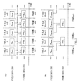
- FIG. 1 is a block diagram illustrating a configuration example of an image pickup device according to a first embodiment of the invention.
- FIG. 2 is a conceptual diagram of adding-up processing in the image pickup device.
- FIG. 4 is a diagram illustrating an example of field data 200 in the case where signals are read from pixels at addresses illustrated in FIG. 3 .
- FIG. 5 is a diagram illustrating a sampling centroid in frame data FM 2 n+ 1 obtained by performing adding-up of field data FL 2 n and FL 2 n+ 1.
- FIG. 6 is a diagram illustrating an example of reset (electronic shutter) and readout timings of each pixel in the image pickup device according to the first embodiment.
- FIG. 7 is a diagram illustrating an example of readout addresses in each field in an image pickup device according to a second embodiment of the invention.
- FIG. 8 is a diagram illustrating sampling centroids at pixel addresses in frame data FM 2 n+ 1 in the second embodiment.
- FIG. 9 is a diagram illustrating an example of reset (electronic shutter) and readout timings of each pixel in the second embodiment.
- FIG. 10 is a diagram illustrating an example in the case where adding-up processing for two pixels is performed in a H1 ⁇ 4V1 ⁇ 4 selective readout mode in a third embodiment.
- FIG. 1 is a block diagram illustrating a configuration example of an image pickup device according to a first embodiment of the invention.
- the image pickup device 100 includes an image pickup optical system 110 , a photoelectric conversion section 120 as a pixel section, a readout circuit 130 , a sampling controller 140 , and a signal processing section 150 .
- the photoelectric conversion section 120 , the readout circuit 130 , the sampling controller 140 , and the signal processing section 150 may be collectively mounted on one chip as a semiconductor element, or may be distributed to a plurality of chips.
- the image pickup device 100 has a function of supporting at least all-pixel readout mode in which signals are read from all pixels and selective readout mode in which signals are intermittently read by skipping a row or a column.
- An operation mode is changed in response to an operation mode control signal 300 supplied from externally of the image pickup device 100 .
- the image pickup device 100 obtains, from the photoelectric conversion section 120 , data different from one field to another, and adds up the data to produce and output frame data.
- the image pickup optical system 110 is configured of a lens, a mechanical shutter, and the like.
- the photoelectric conversion section 120 detects light incident through the image pickup optical system 110 , and generates an electrical signal according to the amount of the light.
- the photoelectric conversion section 120 is configured of, for example, a CMOS (Complementary Metal Oxide Semiconductor) image sensor, and the like.
- CMOS Complementary Metal Oxide Semiconductor
- the photoelectric conversion section 120 includes a number M ⁇ N of pixels arranged in a matrix with M rows and N columns.
- the pixels each include a photoelectric transducer configured of, for example, a photodiode generating a charge according to the amount of incident light.
- a color filter array in which color filters with different spectral transmittances are regularly arranged is disposed in front of the pixels arranged in a matrix.
- the color filter array may use, for example, a Bayer pattern (refer to FIG. 3 or FIG. 4 which will be described later) configured of RGB color filters, or a complementary color filter configured of CMYG color filters.
- the readout circuit 130 reads an analog electrical signal generated in the photoelectric conversion section 120 , and performs AD (Analog/Digital) conversion on the analog electrical signal to output a resultant signal as field data 200 .
- AD Analog/Digital
- the sampling controller 140 controls, in response to the operation mode control signal 300 , to select a pixel from which a signal is to be read from the pixels arranged in a matrix with M rows and N columns.
- the sampling controller 140 sequentially reads signals from all pixels when the operation mode control signal 300 designates all-pixel readout mode.
- the sampling controller 140 controls to read a signal from a different pixel while varying a readout position from one field to another when the operation mode control signal 300 designates selective readout mode.
- the sampling controller 140 performs the following process.
- the sampling controller 140 reads data from 4 x -th rows in a field 2 a , and reads signals from 4 x+ 2-th rows in a field 2 a+ 1.
- a and x each are an arbitrary integer.
- the photoelectric conversion section 120 outputs, in response to a signal from the sampling controller 140 , an electrical signal from a pixel 121 located in a specific row to the readout circuit 130 .
- the readout circuit 130 reads the electrical signal from the specific row in response to a control signal CTL from the sampling controller 140 , and performs AD conversion on the electrical signal to output a resultant signal as field data 200 .
- the readout circuit 130 may read electrical signals from all columns in response to a control signal CLT from the sampling controller 140 , and may perform AD conversion on the electrical signals, and output only a resultant signal from a specific column as the field data 200 .
- the signal processing section 150 performs signal processing on the field data 200 supplied from the readout circuit 130 to output resultant data as frame data 210 to an external device.
- the signal processing section 150 includes an adding-up section 151 and a memory 152 , and selects, in response to the operation mode control signal 300 , whether to add up plural sets of field data 200 over a plurality of fields to output resultant data.
- the signal processing section 150 performs signal processing only on a set of field data 200 of a single field to output resultant data as frame data 210 .
- the signal processing section 150 adds up plural sets of field data 200 over a plurality of fields to output resultant data as frame data 210 .
- the memory 152 of the signal processing section 150 temporarily stores the field data 200 supplied from the readout circuit 130 .
- the adding-up section 151 of the signal processing section 150 adds up plural sets of field data 200 stored in the memory 152 or supplied from the readout circuit 130 .
- the adding-up section 151 performs adding-up (or averaging) of data at a corresponding coordinate over a plurality of fields for each of all pixels. Then, a single set of image data is produced from plural sets of image data.
- the adding-up section 151 adds up m sets of field data 200 to produce one set of image data.
- the memory 152 it is necessary for the memory 152 to store m ⁇ 1 sets or more of field data 200 .
- the image pickup device 100 changes the readout position from one field to another in selective readout mode, and adds up plural sets of the field data 200 over a plurality of fields to produce the frame data 210 .
- one to n ⁇ (m ⁇ 1) frames of frame data are allowed to be obtained from n fields of field data 200 .
- the number of frames of frame data 210 to be obtained from n fields of the field data 200 is allowed to be freely determined by a necessary frame rate or the like.
- FIGS. 2(A) and 2(B) are conceptual diagrams of the adding-up processing in the image pickup device.
- FIG. 2(A) illustrates an example of the case where (n ⁇ 1) frames of frame data 210 are produced from n fields of the field data 200 .
- Frame data Fmn in a frame n is produced by performing adding-up of field data FLn in a field n and field data FLn ⁇ 1 in a field n ⁇ 1.
- frame data FMn+1 in a frame n+1 is produced by performing adding-up of field data FLn+1 and FLn.
- FIG. 2(B) illustrates an example of the case where n frames of frame data 210 are produced from 2 n fields of field data 200 .
- Frame data FMn in the frame n is produced by performing adding-up of field data FL 2 n and FL 2 n+ 1.
- the frame data FMn+1 in the frame n+1 is produced by performing adding-up of field data FL 2 ( n+ 1) and FL 2 ( n+ 1)+1.
- the image pickup device 100 When adding-up of the field data FLn in the field n and the field data FLn ⁇ 1 in the field n ⁇ 1 is performed to produce frame data FMn in the frame n, the image pickup device 100 adds up data at a same address.
- FIGS. 3(A) and 3(B) illustrate readout addresses in a field 2 n and readout addresses in a field 2 n+ 1, respectively.
- n is an arbitrary integer.
- signals are read from pixels at intersection points of a 4 x 2 j -th row and a 4 x ( 2 j+ 1)+1-th row, and a 4 x 2 i -th column and a 4 x ( 2 i+ 1)+1-th column in pixels arranged in a matrix with M rows and N columns.
- i and j each are an arbitrary integer satisfying 4 x ( 2 j+ 1)+3 ⁇ M, and 4 x ( 2 i+ 1)+3 ⁇ N.
- signals are read from pixels at intersection points of a 4 x 2 j+ 2-th row and a 4 x ( 2 j+ 1)+1-th row, and a 4 x 2 i+ 2-th column and a 4 x ( 2 i+ 1)+1-th column.
- the image pickup device 100 changes the readout positions of pixels in an odd-numbered row 2 j and an odd-numbered column 2 i from one field to another in selective readout mode.
- FIGS. 4(A) and 4(B) illustrate an example of the field data 200 in the case where signals are read from pixels at addresses illustrated in FIG. 3 .
- data from pixels in a 4 x 2 j -th row and data from pixels in a 4 ( 2 j+ 1)+1-th row are supplied to an even-numbered row 2 j and an odd-numbered row 2 j+ 1, respectively, in the field data FL 2 n in the field 2 n.
- Data from pixels in a 4 x 2 i -th column and data from pixels in a 4 ( 2 i+ 1)+1-th column are supplied to an even-numbered column 2 i and an odd-numbered column 2 i+ 1, respectively.
- data from pixels in a 4 x 2 j+ 2-th row and data from pixels in a 4 ( 2 j+ 1)+1-th row are supplied to an even-numbered row 2 j and an odd-numbered row 2 j+ 1, respectively, in the field data FL 2 n+ 1 in the field 2 n+ 1.
- Data from pixels in a 4 x 2 i+ 2-th column and data from pixels in a 4 ( 2 i+ 1)+1-th column are supplied to an even-numbered column 2 i and an odd-numbered column 2 i+ 1, respectively.
- plural sets of field data 200 with different readout positions are added up to allow sampling centroids in even-numbered rows and sampling centroids in odd-numbered rows to have an equal pitch.
- FIG. 5 illustrates a sampling centroid in frame data FM 2 n+ 1 obtained by performing adding-up of the field data FL 2 n and FL 2 n+ 1.
- the row address of a pixel from which data is supplied to an even-numbered row 2 j in the field data FL 2 n is 4 x 2 j
- the row address of a pixel from which data is supplied to an even-numbered row 2 j in the field data FL 2 n+ 1 is 4 x 2 j+ 2.
- the row address of a pixel from which data is supplied to an odd-numbered row 2 j+ 1 is 4 x ( 2 j+ 1)+1 in both of the field data FL 2 n and FL 2 n+ 1, and the centroid is not changed even after adding-up.
- a sampling centroid in a k-th row (k is an arbitrary integer satisfying 0 ⁇ 4 k ⁇ M) in the frame data FM 2 n+ 1 is 4 k+ 1 in both of even-numbered rows and odd-numbered rows, and centroid displacement in rows is eliminated.
- the column address of a pixel from which data is supplied to an even-numbered column 2 i in the field data FL 2 n is 4 x 2 i
- the column address of a pixel from which data is supplied to an even-numbered row 2 i in the field data FL 2 n+ 1 is 4 x 2 i+ 2.
- the column address of a pixel from which data is supplied to an odd-numbered column 2 i+ 1 is 4 x ( 2 j+ 1) in both of the field data FL 2 n and FL 2 n+ 1, and the centroid is not changed even after adding-up.
- the image pickup device 100 adds up plural sets of field data 200 with different readout positions to produce the frame data 210 , thereby allowing sampling centroids of pixels in rows and sampling centroids of pixels in columns to be fixed, and reducing jaggies.
- a pixel readout address to be designated for readout in each field may be selected to allow centroids in rows and centroids in columns to be fixed, and is not limited to the examples in FIGS. 3 to 5 .
- the S/N ratio of the frame data 210 is improved.
- output values of respective pixels in the fields 2 n and 2 n+ 1 are equal and SFD, and noise is NFD.
- FIG. 6 illustrates an example of reset (electronic shutter) and readout timings of each pixel in the image pickup device 100 .
- a horizontal axis and a vertical axis indicate time and the row address of a pixel, respectively.
- Data is read from a pixel at a row address 0 at the beginning of the field 2 n .
- data is read from a pixel at a row address 2 at the beginning of the field 2 n+ 1.
- signals are read from a same pixel at a row address 4 ( i+ 1)+1 in an odd-numbered row 2 i+ 1 in fields 2 n and 2 n+ 1.
- a storage time Te from resetting an electrical signal from each pixel to reading a signal is necessary to be shorter than a field period Tf, i.e., a length of one field.
- sampling centroids of pixels in rows are allowed to be fixed, and jaggies are allowed to be reduced.
- the S/N ratio and image quality are allowed to be improved.
- An image pickup device 100 A is similar to that in the first embodiment in that the image pickup device 100 A supports at least all-pixel readout mode in which signals are read from all pixels and selective readout mode in which signals are intermittently read by skipping a row or a column, and is allowed to control an operation mode by the operation mode control signal 300 .
- the image pickup device 100 A obtains, from the photoelectric conversion section 120 , data different from one filed to another, and adds up the data to produce and output frame data.
- the image pickup device 100 A adds up plural sets of field data 200 to produce frame data.
- the image pickup device 100 A adds up data at a same address in field data.
- FIG. 7 illustrates an example of readout addresses in each field in the image pickup device according to the second embodiment of the invention.
- data is read from pixel addresses different from one of a plurality of fields being to be subjected to adding-up to another of the plurality of fields.
- a signal is read from a pixel at a row address 4 x 2 j in an even-numbered row 2 i of field data FD 2 n in the field 2 n , and a signal is read from a pixel at a row address 4 x 2 j+ 3 in an odd-numbered row 2 i+ 1.
- a signal is read from a pixel at a row address 4 x 2 j+ 2 in an even-numbered row 2 i in field data FD 2 n+ 1 in the field 2 n+ 1, and a signal is read from a pixel at a row address 4 x ( 2 j+ 1)+3 in an odd-numbered row 2 i+ 1.
- Signals are read from pixels at intersection points of a 4 x 2 j -th row and a 4 x 2 j+ 3-th row, and a 4 x 2 i -th column and a 4 x ( 2 i+ 1)+1-th column in pixels arranged in a matrix with M rows and N columns.
- i and j each are an arbitrary integer satisfying 4 x ( 2 j+ 1)+3 ⁇ M and 4 x ( 2 i+ 1)+3 ⁇ N.
- signals are read from pixels at intersection points of a 4 x 2 j+ 2-th row and a 4 x ( 2 j+ 1)+3-th row, and a 4 x 2 i+ 2-th column and a 4 x ( 2 i+ 1)+1-th column.
- data from pixels in the 4 x 2 i -th column and data in the 4 ( 2 i+ 1)+1-th column are supplied to an even-numbered column 2 i and an odd-numbered column 2 i+ 1, respectively, in field data FL 2 n.
- the second embodiment is similar to the first embodiment in that data from a pixel in the 4 x 2 i+ 2-th column and data from a pixel in the 4 ( 2 i+ 1)+1-th column are supplied to an even-numbered column 2 i and an odd-numbered column 2 i+ 1, respectively, in field data FL 2 n+ 1.
- the addresses of pixels from which data is to be read in all of R, G and B pixels are different between the field 2 n and the field 2 n+ 1.
- the address of each pixel is represented by (column address of the pixel, row address of the pixel).
- FIG. 8 illustrates sampling centroids at pixel addresses in frame data FM 2 n+ 1.
- a centroid in an even-numbered row 2 i is located at a pixel at a row address 4 x 2 i+ 1, because the row address of a pixel in the field 2 n is 4 x 2 i , and the row address of a pixel in the field 2 n+ 1 is 4 x 2 i+ 2.
- a centroid in an odd-numbered row 2 i+ 1 is located at a pixel at a row address 4 x ( 2 i+ 1)+1, because the row address of a pixel in the field 2 n is 4 x 2 i+ 3, and the row address of a pixel in the field 2 n+ 1 is 4 x ( 2 i+ 1 )+3.
- a sampling centroid in a k-th row (k is an arbitrary integer satisfying 0 ⁇ 4 k ⁇ M) in the frame data FM 2 n+ 1 is 4 k+ 1 in both of even-numbered rows and odd-numbered rows, and centroid displacement in rows is eliminated.
- the column address of a pixel from which data is supplied to an even-numbered column 2 i in the field data FL 2 n is 4 x 2 i
- the column address of a pixel from which data is supplied to an even-numbered column 2 i in the field data FL 2 n+ 1 is 4 x 2 i+ 2.
- the column address of a pixel from which data is supplied to an odd-numbered row 2 i+ 1 is 4 x ( 2 j+ 1)+1 in both of the field data FL 2 n and FL 2 n+ 1, and the centroid is not changed even after adding-up.
- a sampling centroid in an 1-th row (L is an arbitrary integer satisfying 0 ⁇ 4 l ⁇ N) in the frame data FM 2 n+ 1 is 4 l+ 1 in both of even-numbered columns and odd-numbered columns, and centroid displacement in columns is eliminated.
- the image pickup device 100 adds up plural sets of field data 200 with different readout positions to produce the frame data 210 , thereby allowing sampling centroids of pixels in rows and sampling centroids in columns of pixels to be fixed, and reducing jaggies.
- a pixel address to be designated for readout in each field may be selected to allow centroids in rows and centroids in columns to be fixed, and is not limited to the examples in FIGS. 3 to 5 .
- the S/N ratio of the frame data 210 is improved.
- signals are read from pixels different from one of a plurality of fields being to be subjected to adding-up to another of the plurality of fields. Therefore, in respective pixels, signals are allowed to be accumulated during a plurality of fields.
- Te is allowed to be set within a range of 0 ⁇ Te ⁇ m ⁇ Tf, where a period of one field is Tf, and the storage time of each pixel is Te.
- FIG. 9 illustrates an example of reset (electronic shutter) and readout timings of each pixel in the second embodiment.
- a horizontal axis and a vertical axis indicate time and the row address of a pixel, respectively.
- Data is read from a pixel at a row address 0 at the beginning of the field 2 n . After that, data is not read from a pixel at the row address 0 until a field 2 n+ 2.
- the pixel at the row address 0 is allowed to be reset from the beginning of the field 2 n to the beginning of the field 2 n+ 2.
- the storage time Te from resetting the electrical signal of each pixel to reading a signal is allowed to be set within a range of a field period Tfx 2 at the maximum.
- the maximum storage time is allowed to be increased by extending the field period Tf; however, a frame rate is reduced.
- the maximum storage time is allowed to be longer than the field period Tf.
- sampling centroids of pixels in rows are allowed to be fixed, and jaggies are allowed to be reduced.
- the S/N ratio and image quality are allowed to be improved.
- the maximum storage time is allowed to be longer than the field period Tf. In other words, while the frame rate is kept unchanged, the maximum storage time is allowed to be increased.
- the sampling controller 140 in the third embodiment controls, in response to the operation mode control signal 400 , to select a pixel from which a signal is to be read from the pixels arranged in a matrix with M rows and N columns.
- the sampling controller 140 sequentially reads signals from all of the pixels when the operation mode control signal 300 designates all-pixel readout mode.
- the sampling controller 140 intermittently selects rows or columns of pixels to read signals from some of pixels.
- the photoelectric conversion section 120 outputs an electrical signal from the pixel 121 located in a specific row to the readout circuit 130 in response to a signal from the sampling controller 140 .
- the readout circuit 130 reads the electrical signal from a specific column in response to the control signal CTL from the sampling controller 140 , and performs AD conversion on the electrical signal to output a resultant signal as field data 200 .
- the readout circuit 130 may read electrical signals from all columns in response to a control signal from the sampling controller 140 , and may perform AD conversion on the electrical signals, and output only a resultant signal from a specific column as the field data 200 .
- the signal processing section 150 performs signal processing on the field data 200 supplied from the readout circuit 130 to output resultant data as frame data 210 to an external device.
- the signal processing section 150 includes the adding-up section 151 and the memory 152 , and selects, in response to the operation mode control signal 300 , whether to perform adding-up of plural sets of pixel data in the field data 200 to output resultant data.
- FIG. 10 illustrates an example of the case where adding-up processing for two pixels is performed in the H1 ⁇ 4V1 ⁇ 4 selective readout mode in the third embodiment.
- the address of each pixel in the field data 200 is represented by (column address of the pixel, row address of the pixel).
- data is read from pixels at ( 4 x 2 i , 4 x 2 j ) and ( 4 x 2 i+ 2, 4 x 2 j+ 2).
- the signal processing section 150 performs adding-up processing for these two pixels to output resultant data as data at ( 2 i , 2 j ) in the frame data 210 .
- adding-up processing for ( 4 x 2 i , 4 x 2 j+ 3) and ( 4 x 2 i+ 2, 4 x ( 2 j+ 1)+3) is performed to output resultant data as data at ( 2 i , 2 j+ 1) in the frame data 210 .
- addition processing for ( 4 x ( 2 i+ 1)+1, 4 x 2 j ) and ( 4 x ( 2 i+ 1)+1, 4 x 2 j+ 2) is performed to output resultant data as data at ( 2 i+ 1, 2 j ) in the frame data 210 .
- adding-up processing for ( 4 x ( 2 i+ 1)+1, 4 x 2 j+ 3) and ( 4 x ( 2 i+ 1)+1, 4 x ( 2 j+ 1)+3) is performed to output resultant data as data at ( 2 i+ 1, 2 j+ 1) in the frame data 210 .
- sampling centroids in rows and sampling centroids in columns in frame data are allowed to be fixed by performing adding-up processing for a plurality of pixels.
- a sampling centroid is located at ( 4 x 2 i+ 1, 4 x 2 j+ 1).
- a sampling centroid is located at ( 4 x 2 ( i+ 1)+1, 4 x 2 ( j+ 1)+1).
- a sampling centroid in a k-th row (k is an arbitrary integer satisfying 0 ⁇ 4 k ⁇ M) in frame data is 4 k+ 1 in both of even-numbered rows and odd-numbered rows.
- a sampling centroid in an 1-th row (L is an arbitrary integer satisfying 0 ⁇ 4 l ⁇ N) is 4 l+ 1 in both of even-numbered columns and odd-numbered columns, and centroid displacement in rows and columns is eliminated.
- an image pickup device 100 B performs adding-up processing for a plurality of pixels in field data 200 to produce the frame data 210 , thereby allowing sampling centroids of pixels in rows and sampling centroids of pixels in columns to be fixed, and reducing jaggies.
- a pixel address to be designated for readout in each field data may be selected to allow centroids in rows and centroids in columns to be fixed, and are not limited to the example in FIG. 10 .
- adding-up is allowed to be performed in each row.
- Such adding-up processing is allowed to be performed sequentially from one row to another. Therefore, it is enough for the memory 152 to have a size for storing data of one row at the minimum.
- adding-up of plural sets of pixel data is performed to produce the frame data 210 , and accordingly, the S/N ratio is allowed to be improved.
- the storage time Te in the image pickup device 100 B is necessary to be shorter than the field period Tf.
- the image pickup device 100 B of the third embodiment adds up plural sets of field data 200 with different readout positions to produce the frame data 210 .
- sampling centroids of pixels in rows are allowed to be fixed, and jaggies are allowed to be reduced.
- the S/N ratio and image quality are allowed to be improved.
- the adding-up processing is allowed to be performed sequentially from one row to another; therefore, the size necessary for the memory 152 is reduced to the size large enough for storing data of one row.
- sampling centroids of pixels in rows are allowed to be fixed, and jaggies are allowed to be reduced.
- the S/N ratio and image quality are allowed to be improved.
- sampling centroids of pixels in rows are allowed to be fixed, and jaggies are allowed to be reduced.
- the S/N ratio and image quality are allowed to be improved.
- the maximum storage time is allowed to be longer than the field period Tf.
- sampling centroids of pixels in rows are allowed to be fixed, and jaggies are allowed to be reduced.
- the S/N ratio and image quality are allowed to be improved.
- the adding-up processing is allowed to be performed sequentially from one row to another; therefore, the size necessary for the memory 152 is reduced to the size large enough for storing data of one row.
Abstract
Description
- 1. First Embodiment (First configuration and function of image pickup device)
- 2. Second Embodiment (Second configuration and function of image pickup device)
- 3. Third Embodiment (Third configuration and function of image pickup device)
Claims (5)
Applications Claiming Priority (4)
| Application Number | Priority Date | Filing Date | Title |
|---|---|---|---|
| JPP2009-223476 | 2009-09-28 | ||
| JP2009223476A JP5625298B2 (en) | 2009-09-28 | 2009-09-28 | Imaging device |
| JP2009-223476 | 2009-09-28 | ||
| PCT/JP2010/065811 WO2011037040A1 (en) | 2009-09-28 | 2010-09-14 | Imaging device |
Publications (2)
| Publication Number | Publication Date |
|---|---|
| US20130016238A1 US20130016238A1 (en) | 2013-01-17 |
| US8830352B2 true US8830352B2 (en) | 2014-09-09 |
Family
ID=43795791
Family Applications (1)
| Application Number | Title | Priority Date | Filing Date |
|---|---|---|---|
| US13/497,373 Expired - Fee Related US8830352B2 (en) | 2009-09-28 | 2010-09-14 | Image pickup device |
Country Status (7)
| Country | Link |
|---|---|
| US (1) | US8830352B2 (en) |
| EP (1) | EP2485476A4 (en) |
| JP (1) | JP5625298B2 (en) |
| KR (1) | KR20120074278A (en) |
| CN (1) | CN102612835A (en) |
| TW (1) | TW201138448A (en) |
| WO (1) | WO2011037040A1 (en) |
Families Citing this family (4)
| Publication number | Priority date | Publication date | Assignee | Title |
|---|---|---|---|---|
| JP5578915B2 (en) * | 2010-04-01 | 2014-08-27 | キヤノン株式会社 | Solid-state imaging device and driving method thereof |
| JP2012175600A (en) | 2011-02-24 | 2012-09-10 | Sony Corp | Imaging apparatus, imaging apparatus control method, and program |
| EP2940992A4 (en) * | 2012-12-25 | 2016-06-08 | Sony Corp | Solid state image-sensing element, method of driving same, and electronic device |
| WO2018051809A1 (en) * | 2016-09-16 | 2018-03-22 | ソニーセミコンダクタソリューションズ株式会社 | Image pickup device and electronic apparatus |
Citations (8)
| Publication number | Priority date | Publication date | Assignee | Title |
|---|---|---|---|---|
| JP2000134549A (en) | 1998-10-22 | 2000-05-12 | Toshiba Corp | Solid-state image pickup device |
| JP2001145025A (en) | 1999-11-12 | 2001-05-25 | Nec Corp | Solid-state image pickup device and its drive method |
| JP2003338933A (en) | 2002-05-20 | 2003-11-28 | Canon Inc | Image control equipment and its control method |
| JP2007104450A (en) | 2005-10-06 | 2007-04-19 | Nippon Hoso Kyokai <Nhk> | Solid-state image pickup device, its device, its driving method, and signal processor |
| JP2007295230A (en) | 2006-04-25 | 2007-11-08 | Matsushita Electric Ind Co Ltd | Solid state imaging apparatus, driving method thereof, and camera |
| WO2008053791A1 (en) | 2006-10-31 | 2008-05-08 | Sanyo Electric Co., Ltd. | Imaging device and video signal generating method employed in imaging device |
| JP2009088940A (en) | 2007-09-28 | 2009-04-23 | Canon Inc | Imaging apparatus and driving method thereof |
| JP2009130580A (en) | 2007-11-22 | 2009-06-11 | Nikon Corp | Imaging element and imaging apparatus |
Family Cites Families (8)
| Publication number | Priority date | Publication date | Assignee | Title |
|---|---|---|---|---|
| US5493335A (en) * | 1993-06-30 | 1996-02-20 | Eastman Kodak Company | Single sensor color camera with user selectable image record size |
| JP4142340B2 (en) * | 2002-05-22 | 2008-09-03 | オリンパス株式会社 | Imaging device |
| JP4190805B2 (en) * | 2002-06-12 | 2008-12-03 | オリンパス株式会社 | Imaging device |
| JP2004266369A (en) * | 2003-02-21 | 2004-09-24 | Sony Corp | Solid-state image pickup unit and its driving method |
| JP3960965B2 (en) * | 2003-12-08 | 2007-08-15 | オリンパス株式会社 | Image interpolation apparatus and image interpolation method |
| JP4416753B2 (en) * | 2006-03-31 | 2010-02-17 | キヤノン株式会社 | Solid-state imaging device |
| JP5053654B2 (en) * | 2007-02-09 | 2012-10-17 | オリンパスイメージング株式会社 | Image processing apparatus and method and electronic camera |
| JP5256725B2 (en) * | 2007-12-25 | 2013-08-07 | 株式会社ニコン | Imaging device |
-
2009
- 2009-09-28 JP JP2009223476A patent/JP5625298B2/en not_active Expired - Fee Related
-
2010
- 2010-09-14 EP EP10818715.4A patent/EP2485476A4/en not_active Withdrawn
- 2010-09-14 KR KR1020127007069A patent/KR20120074278A/en not_active Application Discontinuation
- 2010-09-14 CN CN2010800525495A patent/CN102612835A/en active Pending
- 2010-09-14 US US13/497,373 patent/US8830352B2/en not_active Expired - Fee Related
- 2010-09-14 WO PCT/JP2010/065811 patent/WO2011037040A1/en active Application Filing
- 2010-09-21 TW TW099132092A patent/TW201138448A/en unknown
Patent Citations (9)
| Publication number | Priority date | Publication date | Assignee | Title |
|---|---|---|---|---|
| JP2000134549A (en) | 1998-10-22 | 2000-05-12 | Toshiba Corp | Solid-state image pickup device |
| JP2001145025A (en) | 1999-11-12 | 2001-05-25 | Nec Corp | Solid-state image pickup device and its drive method |
| JP2003338933A (en) | 2002-05-20 | 2003-11-28 | Canon Inc | Image control equipment and its control method |
| JP2007104450A (en) | 2005-10-06 | 2007-04-19 | Nippon Hoso Kyokai <Nhk> | Solid-state image pickup device, its device, its driving method, and signal processor |
| JP2007295230A (en) | 2006-04-25 | 2007-11-08 | Matsushita Electric Ind Co Ltd | Solid state imaging apparatus, driving method thereof, and camera |
| WO2008053791A1 (en) | 2006-10-31 | 2008-05-08 | Sanyo Electric Co., Ltd. | Imaging device and video signal generating method employed in imaging device |
| US20100053356A1 (en) * | 2006-10-31 | 2010-03-04 | Sanyo Electric Co., Ltd | Imaging Device And Video Signal Generating Method Employed In Imaging Device |
| JP2009088940A (en) | 2007-09-28 | 2009-04-23 | Canon Inc | Imaging apparatus and driving method thereof |
| JP2009130580A (en) | 2007-11-22 | 2009-06-11 | Nikon Corp | Imaging element and imaging apparatus |
Non-Patent Citations (2)
| Title |
|---|
| Japanese Patent Office Action issued in connection with related Japanese Patent Application No. JP 2009-223476 dated Dec. 10, 2013. |
| WO 2008053791, Tsunekawa et al., Aug. 5, 2008, Imaging Device and Video Signal Generating Method Employed in Imaging Device. * |
Also Published As
| Publication number | Publication date |
|---|---|
| WO2011037040A1 (en) | 2011-03-31 |
| EP2485476A4 (en) | 2014-10-01 |
| JP2011071927A (en) | 2011-04-07 |
| JP5625298B2 (en) | 2014-11-19 |
| KR20120074278A (en) | 2012-07-05 |
| EP2485476A1 (en) | 2012-08-08 |
| TW201138448A (en) | 2011-11-01 |
| CN102612835A (en) | 2012-07-25 |
| US20130016238A1 (en) | 2013-01-17 |
Similar Documents
| Publication | Publication Date | Title |
|---|---|---|
| JP5342969B2 (en) | Imaging apparatus and imaging method | |
| JP6380974B2 (en) | Imaging device, imaging device | |
| EP3092792B1 (en) | System and method for capturing digital images using multiple short exposures | |
| KR101426198B1 (en) | Imaging device, imaging method and recording medium | |
| EP4160680A1 (en) | Image sensor with wide dynamic range | |
| US20130308044A1 (en) | Imaging apparatus, image sensor, imaging control method, and program | |
| US20120188392A1 (en) | Imaging system with multiple sensors for producing high-dynamic-range images | |
| US9025065B2 (en) | Solid-state imaging device, image processing method, and camera module for creating high dynamic range images | |
| CN103181160B (en) | Imaging device and formation method | |
| US8830384B2 (en) | Imaging device and imaging method | |
| KR20150084638A (en) | Solid-state imaging device and camera system | |
| US9237282B2 (en) | Solid-state imaging device and camera module including AD converting units for respective pixels | |
| US8830352B2 (en) | Image pickup device | |
| JP4419675B2 (en) | Solid-state imaging device and driving method of solid-state imaging device | |
| JP2008278453A (en) | Image sensing apparatus and image capturing system | |
| JP2006020037A (en) | Physical information acquisition method, physical information acquisition device, and semiconductor device for detecting physical quantity distribution | |
| JP7118659B2 (en) | IMAGING DEVICE, IMAGING DEVICE CONTROL METHOD AND PROGRAM | |
| JP6137539B2 (en) | Solid-state imaging device, driving method thereof, and electronic apparatus | |
| JP6257348B2 (en) | Solid-state imaging device, imaging system, and copying machine | |
| JP6736612B2 (en) | Imaging device, imaging device | |
| JP4468052B2 (en) | IMAGING DEVICE AND IMAGING DEVICE CONTROL METHOD | |
| KR20150098547A (en) | Solid-state imaging apparatus and camera system | |
| JP2015173387A (en) | Imaging element, driving method of the same, and program | |
| JP4437503B2 (en) | Imaging device | |
| JP4067544B2 (en) | Imaging device |
Legal Events
| Date | Code | Title | Description |
|---|---|---|---|
| AS | Assignment |
Owner name: SONY CORPORATION, JAPAN Free format text: ASSIGNMENT OF ASSIGNORS INTEREST;ASSIGNORS:EBIHARA, HIROAKI;NITTA, YOSHIKAZU;KITAMI, HIROTAKA;SIGNING DATES FROM 20120403 TO 20120405;REEL/FRAME:029012/0764 |
|
| FEPP | Fee payment procedure |
Free format text: PAYOR NUMBER ASSIGNED (ORIGINAL EVENT CODE: ASPN); ENTITY STATUS OF PATENT OWNER: LARGE ENTITY |
|
| STCF | Information on status: patent grant |
Free format text: PATENTED CASE |
|
| AS | Assignment |
Owner name: SONY SEMICONDUCTOR SOLUTIONS CORPORATION, JAPAN Free format text: ASSIGNMENT OF ASSIGNORS INTEREST;ASSIGNOR:SONY CORPORATION;REEL/FRAME:040419/0001 Effective date: 20161006 |
|
| MAFP | Maintenance fee payment |
Free format text: PAYMENT OF MAINTENANCE FEE, 4TH YEAR, LARGE ENTITY (ORIGINAL EVENT CODE: M1551) Year of fee payment: 4 |
|
| FEPP | Fee payment procedure |
Free format text: MAINTENANCE FEE REMINDER MAILED (ORIGINAL EVENT CODE: REM.); ENTITY STATUS OF PATENT OWNER: LARGE ENTITY |
|
| LAPS | Lapse for failure to pay maintenance fees |
Free format text: PATENT EXPIRED FOR FAILURE TO PAY MAINTENANCE FEES (ORIGINAL EVENT CODE: EXP.); ENTITY STATUS OF PATENT OWNER: LARGE ENTITY |
|
| STCH | Information on status: patent discontinuation |
Free format text: PATENT EXPIRED DUE TO NONPAYMENT OF MAINTENANCE FEES UNDER 37 CFR 1.362 |
|
| FP | Lapsed due to failure to pay maintenance fee |
Effective date: 20220909 |