WO2011024990A1 - 間引き給電型アレーアンテナ装置 - Google Patents
間引き給電型アレーアンテナ装置 Download PDFInfo
- Publication number
- WO2011024990A1 WO2011024990A1 PCT/JP2010/064675 JP2010064675W WO2011024990A1 WO 2011024990 A1 WO2011024990 A1 WO 2011024990A1 JP 2010064675 W JP2010064675 W JP 2010064675W WO 2011024990 A1 WO2011024990 A1 WO 2011024990A1
- Authority
- WO
- WIPO (PCT)
- Prior art keywords
- array antenna
- antenna apparatus
- feed
- type array
- feed type
- Prior art date
- Legal status (The legal status is an assumption and is not a legal conclusion. Google has not performed a legal analysis and makes no representation as to the accuracy of the status listed.)
- Ceased
Links
Images







Classifications
-
- H—ELECTRICITY
- H01—ELECTRIC ELEMENTS
- H01Q—ANTENNAS, i.e. RADIO AERIALS
- H01Q9/00—Electrically-short antennas having dimensions not more than twice the operating wavelength and consisting of conductive active radiating elements
- H01Q9/04—Resonant antennas
- H01Q9/16—Resonant antennas with feed intermediate between the extremities of the antenna, e.g. centre-fed dipole
- H01Q9/20—Two collinear substantially straight active elements; Substantially straight single active elements
- H01Q9/24—Shunt feed arrangements to single active elements, e.g. for delta matching
-
- H—ELECTRICITY
- H01—ELECTRIC ELEMENTS
- H01Q—ANTENNAS, i.e. RADIO AERIALS
- H01Q19/00—Combinations of primary active antenna elements and units with secondary devices, e.g. with quasi-optical devices, for giving the antenna a desired directional characteristic
- H01Q19/10—Combinations of primary active antenna elements and units with secondary devices, e.g. with quasi-optical devices, for giving the antenna a desired directional characteristic using reflecting surfaces
-
- H—ELECTRICITY
- H01—ELECTRIC ELEMENTS
- H01Q—ANTENNAS, i.e. RADIO AERIALS
- H01Q21/00—Antenna arrays or systems
- H01Q21/06—Arrays of individually energised antenna units similarly polarised and spaced apart
- H01Q21/061—Two dimensional planar arrays
- H01Q21/062—Two dimensional planar arrays using dipole aerials
-
- H—ELECTRICITY
- H01—ELECTRIC ELEMENTS
- H01Q—ANTENNAS, i.e. RADIO AERIALS
- H01Q21/00—Antenna arrays or systems
- H01Q21/06—Arrays of individually energised antenna units similarly polarised and spaced apart
- H01Q21/08—Arrays of individually energised antenna units similarly polarised and spaced apart the units being spaced along or adjacent to a rectilinear path
Definitions
- the present invention relates to a thinning-feed type array antenna apparatus, and more particularly to a thinning-feed type array antenna apparatus in which a plurality of feeding elements and parasitic elements are arranged on a reflector.
- Patent Document 1 and Patent Document 2 a plurality of feeding elements and parasitic elements are arranged, and side lobes radiated from the feeding elements are used to electromagnetically (spatically) feed elements and parasitic elements.
- An array antenna is disclosed that is coupled to reduce the feed section. In these elements, a feeding element and a parasitic element are arranged at a predetermined interval on a substantially parallel same plane that is separated from the reflecting surface of the reflecting plate by a predetermined distance.
- Patent Document 1 and Patent Document 2 are electromagnetically (spatially) coupled to parasitic elements using side lobes of the feeding elements, the distance from the reflector and the feeding elements The distance between the parasitic elements needs to be determined strictly. For this reason, the degree of freedom in design is poor, and it is difficult to manufacture each element because it is necessary to arrange each element so as to float from the reflector using a conductor or the like. Furthermore, since the height of each element from the reflecting plate needs to be high to some extent, it cannot be lowered, and there is a limit to reducing the thickness. Furthermore, since each element is spatially coupled, the design is difficult and not practical for application to an antenna arranged on a curved surface such as a conformal array antenna.
- the present invention intends to provide a thinned-feed type array antenna apparatus that has a high degree of design freedom and can be thinned.
- a thinned-feed type array antenna apparatus includes a reflecting plate, a feeding element that is disposed on the reflecting plate and has a feeding point in the center, and a predetermined amount from the feeding element.
- the parasitic element is arranged on the reflector parallel to the feeding element with a gap between the feeding element and the feeding element and the parasitic element. And a differential transmission path for connecting the elements.
- a substrate may be provided, the reflecting plate may be provided on the back surface of the substrate, and the feeding element and the parasitic element may be provided on the surface of the substrate.
- differential transmission path may be provided on the front surface of the substrate or on the back surface of the substrate through a via hole provided in the substrate.
- the substrate may have plasticity.
- a plurality of feeding elements and parasitic elements may be alternately arranged continuously.
- a plurality of parasitic elements may be continuously arranged, and the differential transmission path may also connect adjacent parasitic elements.
- a shield member may be provided on the differential transmission path.
- the feed element has an element length of approximately ⁇ / 2 (where ⁇ is the wavelength of the radiated wave), and the length of the differential transmission path between the feed element and the parasitic element is an integral multiple of ⁇ . good.
- the differential transmission path between the feeding element and the parasitic element may be bent.
- differential transmission line may be provided with an impedance adjustment unit that varies its length for impedance adjustment.
- the feeding element may constitute at least one dipole element of the cross dipole antenna, and the parasitic element may be arranged in parallel to the dipole element configured as the feeding element.
- the feed element constitutes two dipole elements of the cross dipole antenna
- the parasitic element constitutes two parasitic elements of the cross parasitic element
- the two parasitic elements respectively correspond to the cross dipole antennas. You may arrange
- differential transmission line may be bent in a meander shape.
- the thinned-feed type array antenna apparatus of the present invention has advantages in that the degree of freedom in design is high and the thickness can be reduced.
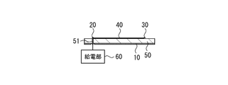
- FIG. 1 is a schematic plan view for explaining the basic configuration of the thinning-feed type array antenna apparatus of the present invention.
- FIG. 2 is a schematic cross-sectional view for explaining the basic configuration of the thinning-feed type array antenna apparatus of the present invention.
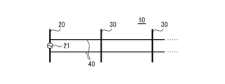
- FIG. 3 is a schematic plan view for explaining an example in which a plurality of feed elements and parasitic elements are alternately arranged continuously in the thinned-feed array antenna apparatus of the present invention.
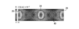
- FIG. 4 is a near magnetic field distribution diagram of the thinning-feed type array antenna apparatus of the present invention.
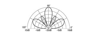
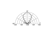
- FIG. 5 shows a radiation pattern of the thinned-feed array antenna apparatus of the present invention.
- FIG. 6 is a graph showing the relationship of the maximum current value with respect to the spacing between lines of the differential transmission path.
- FIG. 1 is a schematic plan view for explaining the basic configuration of the thinning-feed type array antenna apparatus of the present invention.
- FIG. 2 is a schematic cross-sectional view for explaining the basic configuration of the
- FIG. 7 is a schematic plan view for explaining an example in which a plurality of parasitic elements of the thinning-feed type array antenna apparatus of the present invention are continuously arranged.
- FIG. 8 is a schematic plan view for explaining an example in which a plurality of elements of the thinning-feed type array antenna apparatus of the present invention are arranged in a zigzag shape.
- FIG. 9 is a schematic cross-sectional view for explaining an example in which the substrate of the thinning-feed type array antenna apparatus of the present invention has plasticity.
- FIG. 10 is a schematic perspective view for explaining an example in which a shield member is provided on the differential transmission path of the thinned-feed type array antenna apparatus of the present invention.
- FIG. 11 is a schematic cross-sectional view for explaining an example in which the differential transmission path of the thinned-feed type array antenna apparatus of the present invention is provided on the back surface of the substrate.
- FIG. 12 is a schematic top view for explaining an example in which the feeding element and the parasitic element of the thinning-feed type array antenna apparatus of the present invention are crossed.
- FIG. 13 is a schematic plan view for explaining an example in which the differential transmission path of the thinning-feed type array antenna apparatus of the present invention is bent in a meander shape.
- FIG. 14 shows a radiation pattern when the differential transmission line of the thinning-feed type array antenna apparatus of the present invention is bent in a meander shape.
- FIG. 15 is a schematic plan view for explaining an antenna pattern obtained by bending the differential transmission line of the thinning-feed type array antenna apparatus of the present invention into another meander shape.
- FIG. 16 is a schematic plan view for explaining an antenna pattern obtained by further bending the differential transmission path of the thinning-feed type array antenna apparatus of the present invention into another meander shape.
- FIG. 1 is a schematic plan view for explaining the basic configuration of the thinning-feed type array antenna apparatus of the present invention.
- FIG. 2 is a schematic cross-sectional view through the feeding point for explaining the basic configuration of the thinning-feed type array antenna apparatus of the present invention.
- the thinned-feed type array antenna apparatus of the present invention is mainly composed of a reflecting plate 10, a feed element 20, a parasitic element 30, and a differential transmission path 40.
- the reflector 10 is made of, for example, a conductor, and is used to suppress the radiation in the back direction from the feeding element and improve the gain in the front direction.
- the feeding element 20 is disposed on the reflector 10. And the electric power feeding element 20 has the electric power feeding point 21 in the center part.
- the feeding element 20 is a radiating element in which radio wave energy is supplied to the feeding point 21 by the feeding unit 60. As shown in FIG. 2, when the thinned-feed type array antenna apparatus is formed using the substrate 50, the feed point 21 is connected to the feed unit 60 through the via hole 51.
- the power supply unit 60 includes an electric signal source, an A / D converter, a balun, an amplifier, and the like for supplying radio wave energy to the power supply element 20.
- the array antenna device is configured using the substrate 50.
- the substrate 50 can be mounted if the feeder element can be fixed by a conductive wire or the like connected to the feeding point of the feeder element. Of course, it may be omitted.
- the feeding element 20 having a feeding point in the center a linear dipole antenna element as shown in the drawing is cited.
- the dipole antenna element an element having an element length of approximately ⁇ / 2 (where ⁇ is the wavelength of the radiated wave) is illustrated.
- the feed element used in the present invention is not limited to such a linear dipole antenna element, and any element may be used as long as it has a feed point at the center, such as a meandering dipole antenna element. good.
- the parasitic element 30 is arranged on the reflector 10 in parallel with the feeder element 20 with a predetermined interval from the feeder element 20.
- the parasitic element 30 has a shape in which the feeding point of the feeding element is short-circuited or opened (in the illustrated example, the feeding point is short-circuited), and the radio wave energy from the feeding unit 60 is supplied to the parasitic element 30. It has not been.
- the parasitic element 30 in the illustrated example has an element length substantially the same as that of the feeder element 20. However, the present invention is not limited to this, and the element lengths of the feed element and the parasitic element can be made different in order to increase the bandwidth of the array antenna device.
- the differential transmission line 40 which is the most characteristic part of the thinning-feed type array antenna apparatus of the present invention is interposed between the feed element 20 and the parasitic element 30.
- the differential transmission path 40 is arranged symmetrically with the feeding point 21 of the feeding element 20 and the center point of the parasitic element 30 as the center, and connects between the feeding element 20 and the parasitic element 30.
- the differential transmission line 40 is, for example, a coplanar transmission line or the like, and means two coplanar lines formed of a metal conductor on the substrate 50.
- the differential transmission path 40 is connected in the middle of the elements on both sides symmetrically with the feeding point 21 of the feeding element 20 as the center so that the two lines are in opposite phases. As a result, it is possible to suppress radio waves from being radiated from the differential transmission path 40. Further, the length of the differential transmission path 40 may be an integer multiple of ⁇ , for example.
- the reflector 10 is provided on the back surface (surface opposite to the radiation direction) of the substrate, and the feed element 20 and the parasitic element 30 are the substrate 50. Is provided on the surface (radial surface).
- the differential transmission path 40 is provided on the surface of the substrate 50.
- a via hole 51 is provided at the power feeding point 21 of the power feeding element 20 of the substrate 50, and the power feeding unit 60 is connected through the via hole 51.
- the feed element 20 and the parasitic element 30 are physically coupled by such a differential transmission path 40. Therefore, unlike the prior art, it is not affected by the distance from the reflecting plate and the distance between elements, so that the degree of freedom in design is improved. Further, it can be easily manufactured by etching or the like.
- FIG. 3 is a schematic plan view for explaining an example in which a plurality of feed elements and parasitic elements are alternately arranged continuously in the thinned-feed array antenna apparatus of the present invention.
- the parts denoted by the same reference numerals as those in FIG. the feeding elements 20 and the parasitic elements 30 are alternately arranged, and the respective elements are connected by a differential transmission path 40.
- one parasitic element 30 is sandwiched between the two feeding elements 20, 20, but in this case, a signal from a feeding unit that drives the two feeding elements 20, 20 is used. It is also possible to give a phase difference. Thereby, it is possible to scan the beam from the parasitic element.
- FIG. 4 shows a magnetic field distribution diagram in the vicinity of the thinned-feed array antenna apparatus shown in FIG. This figure shows the simulation results under the following conditions.
- the element length of the feed element 20 and the parasitic element 30 is ⁇ / 2.
- the reflector is infinitely arranged at an interval of ⁇ / 4.
- the distance between the feed element 20 and the parasitic element 30 is ⁇ (that is, a difference)
- the length of the dynamic transmission line 40 is ⁇ )
- the connection point of the differential transmission path 40 to each element 20, 30 is ⁇ a / 2 with the feeding point as the center (Where a is the distance between the lines of the differential transmission path 40)
- the distance a between the differential transmission lines 40 is 0.2 ⁇ .
- FIG. 5 shows a radiation pattern of the thinned-feed array antenna apparatus of the present invention.
- the radiation pattern in the figure is a simulation result of the radiation pattern of each element in the zx plane in FIG.
- the simulation conditions are the same as the conditions in FIG. From the figure, it can be seen that the radiation pattern and the effective gain of the thinned-feed array antenna apparatus of the present invention are substantially the same as those of the all-element-feed array antenna apparatus.
- the side lobe (quantization lobe) of the radiation pattern shown in FIG. 5 will be described.
- quantization lobes appear in addition to the front beam.
- the length of the differential transmission path between the feeding element and the parasitic element is preferably an integer multiple of ⁇ so as to be in phase. Therefore, the thinned-feed array antenna apparatus of the present invention may be formed so that the differential transmission path is bent. That is, when the distance between the feed element and the parasitic element is shorter than the length of the differential transmission path, the differential transmission path between the feed element and the parasitic element is bent to have a predetermined length. As a result, the length of the differential transmission path can be set to ⁇ while the interval between the feeding element and the parasitic element is set to ⁇ / 2, for example.
- each line may be bent in a meander shape.
- the length of the differential transmission line may be varied for impedance adjustment.
- an impedance adjusting unit such as a crank bent portion may be provided in the differential transmission path, and impedance matching may be achieved by adjusting the length of the differential transmission path.
- FIG. 6 is a graph showing the relationship of the maximum current value with respect to the spacing between lines of the differential transmission path.
- the interval a between the lines of the differential transmission path may be set to 0.2 ⁇ .
- this specific value is an example to the last, and the space
- the thinning-feed type array antenna apparatus of the present invention may be one in which the feed element and the parasitic element are not alternated as shown in FIG.
- FIG. 7 is a schematic plan view for explaining an example in which a plurality of parasitic elements of the thinned-feed array antenna apparatus of the present invention are continuously arranged.
- the parts denoted by the same reference numerals as those in FIG. As shown in the drawing, a plurality of parasitic elements 30 are continuously arranged with respect to the feeding element 20, and adjacent parasitic elements are also connected by a differential transmission path 40. Even in such a configuration, each parasitic element 30 behaves in the same manner as the feeding element 20 because the feeding element 20 and the parasitic element 30 are coupled by the differential transmission path 40. .
- a plurality of parasitic elements can be radiating elements with one feeding element, it is possible to further reduce the number of feeding parts.
- the appearance pattern of a feeding element and a parasitic element is not limited to the above-mentioned illustration example, You may arrange
- FIG. 8 is a schematic plan view for explaining an example in which a plurality of elements of the thinning-feed type array antenna apparatus of the present invention are arranged in a zigzag shape.
- each element is physically connected by a differential transmission path, so that there is a degree of freedom in the arrangement of the elements, and even if arranged in a zigzag shape, the array antenna apparatus Function as.
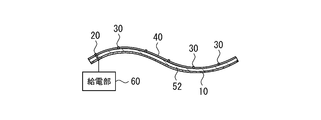
- FIG. 9 shows a schematic cross-sectional view through the feeding point for explaining an example in which the substrate of the thinning-feed type array antenna apparatus of the present invention has plasticity.
- the thinned-feed type array antenna apparatus of the present invention can use a plastic substrate 52, more specifically a flexible printed circuit board. Since the thinned-feed type array antenna apparatus of the present invention physically couples each element using a differential transmission path, it functions as an array antenna without any problem even if the radiation direction of each element changes. is there. Therefore, the present invention can also be applied to an antenna arranged on a curved surface such as a conformal array antenna. In other words, a conformal array antenna can be realized simply by forming the thinning-feed type array antenna device of the present invention on a flexible printed circuit board and pasting it on, for example, the curved surface of an aircraft body.
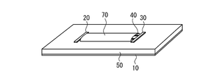
- FIG. 10 is a schematic perspective view for explaining an example in which a shield member is provided on the differential transmission path of the thinned-feed type array antenna apparatus of the present invention.
- the feeding element 20 and the parasitic element 30, and the differential transmission path 40 that connects between them are provided on the surface of the substrate 50 on the radial direction side.
- the shield member 70 is disposed so as to cover the differential transmission path 40.
- the shield member 70 has conductivity, for example. If necessary, the shield member 70 may be electrically connected to the reflecting plate 10 provided on the surface opposite to the radial direction.
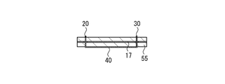
- FIG. 11 is a schematic cross-sectional view passing through one of the differential transmission paths for explaining an example in which the differential transmission path of the thinned-feed type array antenna apparatus of the present invention is provided on the back surface of the substrate.
- the substrate is a three-layer substrate 55, and the feeding element 20 and the parasitic element 30 are provided on the substrate surface.
- the differential transmission path 40 is provided in the back surface of a board
- the reflection plate 17 is disposed in the center layer of the three-layer substrate 55. Thereby, since the radiation to the antenna radiation direction side from the differential transmission path 40 is blocked by the reflecting plate 17, the reflecting plate 17 also serves as the above-described shield member.
- a differential transmission path may be disposed on the back surface of the board, and a power feeding element and a parasitic element may be provided on the surface of the board, and a conductor may be left as a shield member therebetween.
- the feeding element and the parasitic element are dipole antenna elements.
- the present invention is not limited to this, and may be, for example, a cross dipole antenna.
- FIG. 12 is a schematic top view for explaining an example in which the feeding element and the parasitic element of the thinning-feed type array antenna apparatus of the present invention are crossed.
- the feed element and the parasitic element include the cross dipole antenna 25 and the cross parasitic element 35.
- the cross dipole antenna 25 has a feeding point 26 at the center, and is arranged by crossing two dipole elements so as to be spatially orthogonal. Further, the cross parasitic element 35 is also arranged by crossing the parasitic elements so as to be spatially orthogonal.
- the two parasitic elements of the cross parasitic element 35 are arranged in directions parallel to the dipole elements of the cross dipole antenna 25, respectively. These are connected by a plurality of differential transmission lines 45 and 46. That is, in FIG. 12, among the elements that are crossed using a plurality of vertical differential transmission lines 45, the elements in the horizontal direction are connected and crossed using a plurality of differential transmission lines 46 in the horizontal direction. Among the active elements, the vertical elements are connected.
- the two dipole elements orthogonal to each other in the cross dipole antenna do not necessarily need to be fed, and only one of them may be fed. That is, only one dipole element of the cross dipole antenna is fed, and of the two parasitic elements of the cross parasitic element, a parasitic element parallel to the fed dipole element is connected by a differential transmission line. It may be configured as follows. As a result, for example, it is possible to perform thinning power supply for the elements in the vertical direction and supply power individually to the elements in the horizontal direction without performing thinning power supply.
- the thinning-feed type array antenna apparatus of the present invention has a plurality of cross dipole antennas 25 and cross parasitic elements 35 arranged in a matrix so that a large-scale array antenna apparatus can have a very high thinning rate. It becomes possible to drive with.
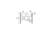
- FIG. 13 is a schematic plan view for explaining an example in which the differential transmission line of the thinning-feed type array antenna apparatus of the present invention is bent in a meander shape.
- the parts denoted by the same reference numerals as those in FIG. Similarly to the above-described example, in the example shown in FIG. 13, a plurality of feeding elements and parasitic elements may be alternately arranged alternately, or a plurality of parasitic elements may be continuously arranged. There may be.
- each line of the differential transmission line 40 is bent and arranged in a meander shape so as to be line-symmetric with respect to the center line between the lines. That is, each track is arranged so as to approach or leave.
- FIG. 14 shows a radiation pattern of the thinning feed type array antenna apparatus shown in FIG. This figure shows the simulation results under the following conditions.
- the element length of the feed element 20 and the parasitic element 30 is ⁇ / 2.
- the reflector is placed infinitely at an interval of ⁇ / 4.
- the distance between the feed element 20 and the parasitic element 30 is ⁇ / 2.
- the length of the differential transmission line 40 is ⁇
- the quantization lobe can be kept small when each line of the differential transmission line is bent in a meander shape.
- FIG. 15 is a schematic plan view for explaining an antenna pattern obtained by bending the differential transmission line of the thinning-feed type array antenna apparatus of the present invention into another meander shape.
- the parts denoted by the same reference numerals as those in FIG. Similarly to the above-described example, in the example shown in FIG. 15, a plurality of feeding elements and parasitic elements may be alternately arranged alternately, or a plurality of parasitic elements may be continuously arranged. There may be.
- the differential transmission line 40 is arranged in a meander shape while maintaining the distance between the lines.
- the entire differential transmission path 40 is bent and arranged in a meander shape.
- the vicinity of the feeding element 20 and the parasitic element 30 is provided with a certain distance compared to the meander portion.
- the present invention is not limited to this, and the range in which the quantization lobe appears may be adjusted by changing the dimension depending on the application. Even with such a configuration, it is possible to realize a thinning-feed type array antenna apparatus having a suppressed quantization lobe radiation pattern as shown in FIG.
- FIG. 16 is a schematic plan view for explaining an antenna pattern obtained by further bending the differential transmission path of the thinning-feed type array antenna apparatus of the present invention into another meander shape.
- the parts denoted by the same reference numerals as those in FIG. Similarly to the above-described example, in the example shown in FIG. 16, a plurality of feeding elements and parasitic elements may be alternately arranged alternately, or a plurality of parasitic elements may be continuously arranged. There may be.
- the differential transmission path 40 is arranged in a meander shape so as to be line symmetric with respect to the center between the feeding element 20 and the parasitic element 30.
- the differential transmission path 40 shown in FIG. 13 is an example in which several stages of meander parts are arranged so as to maintain the same height (length), but what is shown in FIG. The portion is disposed so as to be higher (longer) than the meander portion in the vicinity of the feeding element 20 and the parasitic element 30.
- the present invention is not limited to this, and the range in which the quantization lobes appear may be adjusted by changing the dimensions depending on the application or the like. When configured in this way, the radiation pattern can be adjusted so that the range in which the quantization lobes appear is increased to some extent.
- thinning-feed type array antenna apparatus of the present invention is not limited to the illustrated example described above, and it is needless to say that various modifications can be made without departing from the scope of the present invention.
Landscapes
- Aerials With Secondary Devices (AREA)
- Variable-Direction Aerials And Aerial Arrays (AREA)
Abstract
設計の自由度が高く、薄型化も可能な間引き給電型アレーアンテナ装置を提供する。 間引き給電型アレーアンテナ装置は、反射板10と、給電素子20と、無給電素子30と、差動伝送路40とを具備するものである。給電素子20は、反射板10の上に配置され、中央部に給電点21を有する。無給電素子30は、給電素子20から所定の間隔を開けて給電素子20と平行に反射板10の上に配置される。差動伝送路40は、給電素子20の給電点21と無給電素子30の中心点を中心に挟んで対称に配置され、給電素子20と無給電素子30間を接続する。
Description
本発明は間引き給電型アレーアンテナ装置に関し、特に、給電素子と無給電素子とを反射板の上で複数配置した間引き給電型アレーアンテナ装置に関する。
複数の放射素子を配置して、そのうちの幾つかを無給電素子とすることで、アンテナ利得を低減させることなく、給電部を簡略化するものが従来から知られている。例えば、特許文献1や特許文献2には、給電素子と無給電素子とを複数配置し、給電素子から放射されるサイドローブを用いることで給電素子と無給電素子を電磁気的に(空間的に)結合して給電部を減らしたアレーアンテナが開示されている。これらは、反射板の反射面から所定の距離を離した略平行な同一平面上に、給電素子と無給電素子を所定の間隔を開けて配置されるものである。
特許文献1や特許文献2に開示のアレーアンテナは、給電素子のサイドローブを用いて電磁気的に(空間的に)無給電素子と結合するものであるため、反射板からの距離や給電素子と無給電素子間の距離は厳密に決定される必要があるものであった。このため、設計の自由度に乏しく、また、各素子は導体等を用いて反射板から浮かせて配置される必要があるため、製造も難しかった。さらに、反射板からの各素子の高さがある程度高い必要があるため、低くすることができず、薄型化にも限界があった。またさらに、各素子が空間的に結合されるものであるため、例えばコンフォーマルアレーアンテナのような、曲面上に配置されるアンテナに適用するには設計が困難で現実的ではなかった。
本発明は、斯かる実情に鑑み、設計の自由度が高く、薄型化も可能な間引き給電型アレーアンテナ装置を提供しようとするものである。
上述した本発明の目的を達成するために、本発明による間引き給電型アレーアンテナ装置は、反射板と、反射板の上に配置され、中央部に給電点を有する給電素子と、給電素子から所定の間隔を開けて給電素子と平行に反射板の上に配置される無給電素子と、給電素子の給電点と無給電素子の中心点を中心に挟んで対称に配置され、給電素子と無給電素子間を接続する差動伝送路と、を具備するものである。
さらに、基板を具備し、反射板は基板の裏面に設けられ、給電素子及び無給電素子は基板の表面に設けられても良い。
また、差動伝送路は、基板の表面に、又は基板に設けられるビアホールを介して基板の裏面に設けられても良い。
また、基板は、可塑性を有しても良い。
また、給電素子及び無給電素子は、複数連続的に互い違いに配置されても良い。
また、無給電素子は複数連続的に配置され、差動伝送路は隣り合う無給電素子間も接続するものであっても良い。
さらに、差動伝送路上にシールド部材を具備するものであっても良い。
また、給電素子は略λ/2(但し、λは放射波の波長)の素子長を有し、給電素子と無給電素子間の差動伝送路の長さがλの整数倍であっても良い。
また、給電素子と無給電素子間の間隔が差動伝送路の長さよりも短い場合、給電素子と無給電素子間の差動伝送路が屈曲するように形成されても良い。
また、差動伝送路は、インピーダンス調整用にその長さを可変するインピーダンス調整部を具備するものであっても良い。
また、給電素子が、クロスダイポールアンテナの少なくとも一方のダイポール素子を構成し、無給電素子が、給電素子として構成されるダイポール素子に平行に配置されても良い。
また、給電素子が、クロスダイポールアンテナの2つのダイポール素子を構成し、無給電素子が、クロス無給電素子の2つの無給電素子を構成し、2つの無給電素子は、それぞれクロスダイポールアンテナの各ダイポール素子に平行に配置されても良い。
また、差動伝送路が、メアンダ状に屈曲されても良い。
本発明の間引き給電型アレーアンテナ装置には、設計の自由度が高く、薄型化も可能であるという利点がある。
以下、本発明を実施するための形態を図示例と共に説明する。図1は、本発明の間引き給電型アレーアンテナ装置の基本構成を説明するための概略平面図である。また、図2は、本発明の間引き給電型アレーアンテナ装置の基本構成を説明するための、給電点を通る概略横断面図である。図示の通り、本発明の間引き給電型アレーアンテナ装置は、反射板10と、給電素子20と、無給電素子30と、差動伝送路40とから主に構成されている。
反射板10は、例えば導体からなるものであり、給電素子からの背面方向の放射を抑制して正面方向の利得を向上させるために用いられる。
給電素子20は、反射板10の上に配置されるものである。そして、給電素子20は、その中央部に給電点21を有する。給電素子20は、給電部60により電波エネルギが給電点21に供給される放射素子である。図2に示されるように、基板50を用いて間引き給電型アレーアンテナ装置が形成される場合には、給電点21はビアホール51を介して給電部60に接続される。給電部60には、給電素子20に電波エネルギを供給するための電気信号源やA/D変換器、バラン、アンプ等が含まれる。
なお、図示例では基板50を用いてアレーアンテナ装置を構成しているが、本発明はこれに限定されず、給電素子の給電点に接続される導線等により給電素子が固定できれば、基板50を省略しても勿論良い。
中央部に給電点を有する給電素子20の具体例としては、図示例のような直線状のダイポールアンテナ素子が挙げられる。ダイポールアンテナ素子としては、略λ/2(但し、λは放射波の波長)の素子長を有するものを図示した。しかしながら、本発明に用いられる給電素子はこのような直線状のダイポールアンテナ素子に限定されず、メアンダ状のダイポールアンテナ素子等、中央部に給電点を有するものであれば、如何なるものであっても良い。
無給電素子30は、給電素子20から所定の間隔を開けて給電素子20と平行に反射板10の上に配置されるものである。無給電素子30は、給電素子の給電点が短絡又は開放された形状を有しており(図示例は給電点が短絡された例)、無給電素子30には給電部60による電波エネルギは供給されていない。図示例の無給電素子30は、給電素子20と略同様の素子長を有するものを示した。しかしながら、本発明はこれに限定されず、アレーアンテナ装置の広帯域化を図る等のため、給電素子と無給電素子の素子長を異ならせることも可能である。
そして、本発明の間引き給電型アレーアンテナ装置の最も特徴的な部分である差動伝送路40が、給電素子20と無給電素子30の間に介在している。差動伝送路40は、給電素子20の給電点21と無給電素子30の中心点を中心に挟んで対称に配置され、給電素子20と無給電素子30間を接続するものである。差動伝送路40とは、例えばコプレナ伝送路等であり、基板50上に金属導体により形成された2本の共平面線路を意味する。差動伝送路40は、2本の線路が逆位相となるように、給電素子20の給電点21を中心に挟んで対称に、両側の素子の途中に接続されている。これにより、差動伝送路40から電波が放射されるのを抑制することが可能となる。また、差動伝送路40の長さは、例えばλの整数倍であれば良い。
図2に示されるように、本発明の間引き給電型アレーアンテナ装置は、反射板10が基板の裏面(放射方向の反対側の面)に設けられ、給電素子20及び無給電素子30が基板50の表面(放射方向側の面)に設けられている。そして、差動伝送路40は、基板50の表面に設けられている。そして、基板50の給電素子20の給電点21のところにビアホール51が設けられており、ビアホール51を介して給電部60が接続される。このように、基板上に 所望の配線パターンをエッチング等により形成するだけで、間引き給電型アレーアンテナ装置が実現可能である。
本発明の間引き給電型アレーアンテナ装置は、このような差動伝送路40により、給電素子20と無給電素子30が、物理的に結合される。したがって、従来技術のように反射板からの距離や素子間の距離に影響を受けないため、設計の自由度が向上する。さらに、エッチング等により容易に製造も可能である。
また、このような基本構成の素子を複数並べることで、大規模なアレーアンテナ装置を実現可能となる。図3は、本発明の間引き給電型アレーアンテナ装置において、給電素子と無給電素子が複数連続的に互い違いに配置される例を説明するための概略平面図である。図中、図1等と同一の符号を付した部分は同一物を表わしているため、詳説は省略する。図示の通り、給電素子20と無給電素子30が互い違いに配置されると共に、差動伝送路40によりそれぞれの素子が接続されている。なお、図中、2つの給電素子20,20に1つの無給電素子30が挟まれるような構成となっているが、この場合、2つの給電素子20,20を駆動する給電部からの信号に、位相差を与えることも可能である。これにより、無給電素子からのビームを走査することも可能となる。
ここで、図3に示される間引き給電型アレーアンテナ装置の近傍磁界分布図を図4に示す。同図は、以下の条件の場合のシミュレーション結果である。
・給電素子20及び無給電素子30の素子長がλ/2の長さ
・反射板は無限大としてλ/4の間隔で配置
・給電素子20と無給電素子30の間隔はλ(即ち、差動伝送路40の長さはλ)
・差動伝送路40の各素子20,30への接続点は給電点を中心に±a/2
(但し、aは差動伝送路40の線路間の間隔)
・差動伝送路40の線路間の間隔aは0.2λ
・給電素子20及び無給電素子30の素子長がλ/2の長さ
・反射板は無限大としてλ/4の間隔で配置
・給電素子20と無給電素子30の間隔はλ(即ち、差動伝送路40の長さはλ)
・差動伝送路40の各素子20,30への接続点は給電点を中心に±a/2
(但し、aは差動伝送路40の線路間の間隔)
・差動伝送路40の線路間の間隔aは0.2λ
図示の通り、上述のような条件において、給電素子20上及び無給電素子30上のそれぞれに大きな電流が分布していることが分かる。また、給電素子20と無給電素子30の最大電流は略同等となっていることが分かる。即ち、給電部を間引いても、無給電素子は給電素子と同等の振る舞いをしていることが分かる。
また、図5に、本発明の間引き給電型アレーアンテナ装置の放射パターンを示す。なお、同図の放射パターンは、図3におけるz-x面内の各素子の放射パターンのシミュレーション結果である。また、シミュレーション条件は図4の条件と同様である。同図から、本発明の間引き給電型アレーアンテナ装置の放射パターン及びその実効利得は、全素子給電型アレーアンテナ装置と略同様であることが分かる。
ここで、図5に示される放射パターンのサイドローブ(量子化ローブ)について説明する。図5に示される放射パターンのように、正面のビーム以外に量子化ローブが現れている。用途によってはこのような特性でも問題ないが、量子化ローブの出る範囲を抑制することも可能である。量子化ローブの出ない範囲、即ち、ビームを振ることが可能な範囲φは、以下の式で定義されるように、給電素子20と無給電素子30の間の間隔dで決定される。
(cosφ+sinφ)d/λ=1
(cosφ+sinφ)d/λ=1
したがって、例えばd=λ/2とすれば、量子化ローブを小さくすることが可能となる。ここで、給電素子と無給電素子間の差動伝送路の長さは、同相となるようにλの整数倍であることが好ましい。そこで、本発明の間引き給電型アレーアンテナ装置は、差動伝送路が屈曲するように形成されても良い。即ち、給電素子と無給電素子間の間隔が差動伝送路の長さよりも短い場合、給電素子と無給電素子間の差動伝送路を屈曲させ、所定の長さとなるように形成される。これにより、給電素子と無給電素子間の間隔を、例えばλ/2としつつ、差動伝送路の長さをλとすることが可能となる。差動伝送路を屈曲させる場合には、例えば各線路をメアンダ状に屈曲させれば良い。
また、インピーダンス調整用に差動伝送路の長さを可変しても良い。例えば、差動伝送路にクランク曲がり部等のインピーダンス調整部を設け、差動伝送路の長さを調整してインピーダンスマッチングを図るようにしても良い。
次に、差動伝送路の線路間の間隔について説明する。差動伝送路の線路間の間隔を変化させると、給電素子及び無給電素子上の電流が変化する。図6は、差動伝送路の線路間の間隔に対する最大電流値の関係を示すグラフである。図示の通り、差動伝送路の線路間の間隔aが0.2λのときに、給電素子と無給電素子の最大電流が略同程度となっている。したがって、差動伝送路において、給電素子と無給電素子を同じような電流分布とする場合には、差動伝送路の線路間の間隔aを0.2λとすれば良い。なお、この具体的な値はあくまでも一例であり、本発明における差動伝送路の線路間の間隔がこの値に限定されるものではない。
さらに、本発明の間引き給電型アレーアンテナ装置は、給電素子と無給電素子が図3に示されるように互い違いではなく、無給電素子が複数連続的に配置されるものであっても良い。図7に、本発明の間引き給電型アレーアンテナ装置の無給電素子が複数連続的に配置される例を説明するための概略平面図を示す。図中、図1等と同一の符号を付した部分は同一物を表わしているため、詳説は省略する。図示の通り、給電素子20に対して無給電素子30が複数連続的に配置されると共に、差動伝送路40により隣り合う無給電素子間も接続されている。このような構成であっても、差動伝送路40により給電素子20と無給電素子30間が結合されているため、各無給電素子30は、給電素子20と同等の振る舞いをすることになる。このように1つの給電素子で複数の無給電素子を放射素子とできることから、給電部をさらに減少させることも可能となる。なお、給電素子と無給電素子の出現パターンは、上述の図示例には限定されず、ランダムに配置されても良い。
また、上述の図示例では、平行且つ直線的に複数の素子が配置される間引き給電型アレーアンテナ装置を示していたが、本発明はこれに限定されない。例えば、本発明の間引き給電型アレーアンテナ装置の複数の素子はジグザク状に配置されても良い。図8は、本発明の間引き給電型アレーアンテナ装置の複数の素子をジグザグ状に配置した例を説明するための概略平面図である。図中、図1等と同一の符号を付した部分は同一物を表わしているため、詳説は省略する。従来の空間的に結合したアレーアンテナ装置では、サイドローブを用いて各素子間を結合させていたため、ジグザグ状に配置するとうまく結合しない場合があった。しかしながら、本発明の間引き給電型アレーアンテナ装置では、各素子間は差動伝送路により物理的に接続されているため、素子の配置に自由度があり、ジグザグ状に配置したとしてもアレーアンテナ装置として機能する。
次に、図9に、本発明の間引き給電型アレーアンテナ装置の基板が可塑性を有する例を説明するための、給電点を通る概略横断面図を示す。図中、図1等と同一の符号を付した部分は同一物を表わしているため、詳説は省略する。図示の通り、本発明の間引き給電型アレーアンテナ装置では、可塑性を有する基板52、より具体的にはフレキシブルプリント基板等を用いることが可能である。本発明の間引き給電型アレーアンテナ装置は、差動伝送路を用いて各素子間を物理的に結合しているため、各素子の放射方向が変わったとしても問題なくアレーアンテナとして機能するものである。したがって、コンフォーマルアレーアンテナのような、曲面上に配置されるアンテナにも適用可能である。即ち、フレキシブルプリント基板上に本発明の間引き給電型アレーアンテナ装置を形成し、これを例えば航空機の機体の曲面に沿って貼付するだけでコンフォーマルアレーアンテナが実現可能となる。
本発明の間引き給電型アレーアンテナ装置では、素子間を差動伝送路で接続している。差動伝送路は、2本の線路が逆位相となるため、差動伝送路から電波が放射されないように構成されている。しかしながら、何らかの理由で差動伝送路からも放射する可能性がある。そこで、以下に説明する例では、差動伝送路上にシールド部材を設けたものを説明する。図10は、本発明の間引き給電型アレーアンテナ装置の差動伝送路上にシールド部材を設けた例を説明するための概略斜視図である。図中、図1等と同一の符号を付した部分は同一物を表わしているため、詳説は省略する。図示例では、給電素子20と無給電素子30、さらにこれらの間を接続する差動伝送路40が基板50の放射方向側の面に設けられている。そして、シールド部材70が、差動伝送路40を覆うように配置されている。シールド部材70は、例えば導電性を有している。また、必要により、シールド部材70は放射方向の反対側の面に設けられる反射板10に電気的に接続されても良い。このようにシールド部材70により差動伝送路40をシールドすることで、差動伝送路40からの放射の影響を排除することが可能となる。
さらに、多層基板を用いた場合には、差動伝送路を基板の裏面側に設けることも可能である。図11は、本発明の間引き給電型アレーアンテナ装置の差動伝送路を基板の裏面に設ける例を説明するための、差動伝送路の一方を通る概略横断面図である。図中、図1等と同一の符号を付した部分は同一物を表わしているため、詳説は省略する。図示の通り、例えば基板を3層基板55とし、基板表面に給電素子20及び無給電素子30を設ける。そして、ビアホールを介して基板の裏面に差動伝送路40を設ける。さらに、反射板17を、3層基板55の中央の層に配置する。これにより、差動伝送路40からのアンテナ放射方向側への放射が反射板17により遮られるため、反射板17が上述のシールド部材の役割も担うようにもなる。
なお、両面基板の場合には、基板裏面に差動伝送路を配置すると共に、基板表面に給電素子及び無給電素子を設け、この間にシールド部材として導体を残しておくように構成しても良い。
次に、本発明の間引き給電型アレーアンテナ装置の他の例について説明する。上述の図示例では、給電素子及び無給電素子はダイポールアンテナ素子を説明したが、本発明はこれに限定されず、例えばクロスダイポールアンテナであっても良い。図12は、本発明の間引き給電型アレーアンテナ装置の給電素子及び無給電素子がクロスしている例を説明するための概略上面図である。図中、図1等と同一の符号を付した部分は同一物を表わしているため、詳説は省略する。図示例の間引き給電型アレーアンテナ装置は、給電素子及び無給電素子が、クロスダイポールアンテナ25及びクロス無給電素子35からなるものである。即ち、クロスダイポールアンテナ25は、中央に給電点26を有し、2つのダイポール素子を空間的に直交するように交差させて配置されるものである。また、クロス無給電素子35も、無給電素子を空間的に直交するように交差させて配置されるものである。クロス無給電素子35の2つの無給電素子は、それぞれクロスダイポールアンテナ25の各ダイポール素子に平行な方向に配置される。これらの間が、複数の差動伝送路45,46で接続されている。即ち、図12上で、縦方向の複数の差動伝送路45を用いてクロスしている素子のうちの横向きの素子間が接続され、横方向の複数の差動伝送路46を用いてクロスしている素子のうち縦向きの素子間が接続されている。なお、クロスダイポールアンテナの直交する2つのダイポール素子は、それぞれ給電される必要は必ずしもなく、片方のみ給電されても良い。即ち、クロスダイポールアンテナの一方のダイポール素子のみが給電され、クロス無給電素子の2つの無給電素子のうち、給電された一方のダイポール素子に平行な無給電素子が差動伝送路で接続されるように構成されても良い。これにより、例えば垂直方向の素子は間引き給電を行い、水平方向の素子は間引き給電を行わないで個々に給電する、というようなことも可能である。本発明の間引き給電型アレーアンテナ装置は、このような複数のクロスダイポールアンテナ25及びクロス無給電素子35が、複数マトリクス状に配置されることで、大規模なアレーアンテナ装置を非常に高い間引き率で駆動することが可能となる。
次に、上述した量子化ローブを小さくすることが可能な構成として、本発明の間引き給電型アレーアンテナ装置の差動伝送路をメアンダ状に屈曲させた場合について説明する。図13は、本発明の間引き給電型アレーアンテナ装置の差動伝送路をメアンダ状に屈曲させた例説明するための概略平面図である。図中、図1等と同一の符号を付した部分は同一物を表わしているため、詳説は省略する。また、上述の例と同様に、図13に示される例でも、給電素子と無給電素子が複数連続的に互い違いに配置されても良いし、無給電素子が複数連続的に配置されるものであっても良い。図示の通り、この例では、差動伝送路40の各線路を、その線路間の中心線に対して線対称になるようにメアンダ状に屈曲させて配置している。即ち、各線路が近付いたり離れたりするように配置されている。
ここで、図13に示される間引き給電型アレーアンテナ装置の放射パターンを図14に示す。同図は、以下の条件の場合のシミュレーション結果である。
・給電素子20及び無給電素子30の素子長がλ/2の長さ
・反射板は無限大としてλ/4の間隔で配置
・給電素子20と無給電素子30の間隔はλ/2
・差動伝送路40の長さはλ
・給電素子20及び無給電素子30の素子長がλ/2の長さ
・反射板は無限大としてλ/4の間隔で配置
・給電素子20と無給電素子30の間隔はλ/2
・差動伝送路40の長さはλ
図示の通り、差動伝送路の各線路をメアンダ状に屈曲した場合、量子化ローブを小さく抑えることが可能であることが分かる。
さらに、本発明の間引き給電型アレーアンテナ装置の差動伝送路を、他のメアンダ状に屈曲させた場合について説明する。図15は、本発明の間引き給電型アレーアンテナ装置の差動伝送路を他のメアンダ状に屈曲したアンテナパターンを説明するための概略平面図である。図中、図1等と同一の符号を付した部分は同一物を表わしているため、詳説は省略する。また、上述の例と同様に、図15に示される例でも、給電素子と無給電素子が複数連続的に互い違いに配置されても良いし、無給電素子が複数連続的に配置されるものであっても良い。図示の通り、この例では、差動伝送路40を、その各線路の距離を保ったままメアンダ状に屈曲させて配置している。即ち、差動伝送路40全体がメアンダ状に屈曲されて配置されている。なお、図示例では、給電素子20や無給電素子30の近傍はメアンダ部分に比べてある程度の間隔を設けている。また、図中、寸法の一例を示したが、本発明はこれに限定されず、用途等によって、寸法を変化させて量子化ローブの出る範囲を調整しても良い。このような構成であっても、図14に示すような抑制された量子化ローブの放射パターンを有する間引き給電型アレーアンテナ装置が実現可能である。
さらにまた、本発明の間引き給電型アレーアンテナ装置の差動伝送路を、さらに他のメアンダ状に屈曲させた場合について説明する。図16は、本発明の間引き給電型アレーアンテナ装置の差動伝送路をさらに他のメアンダ状に屈曲したアンテナパターンを説明するための概略平面図である。図中、図1等と同一の符号を付した部分は同一物を表わしているため、詳説は省略する。また、上述の例と同様に、図16に示される例でも、給電素子と無給電素子が複数連続的に互い違いに配置されても良いし、無給電素子が複数連続的に配置されるものであっても良い。図示の通り、この例では、差動伝送路40を、給電素子20と無給電素子30の間を中心に線対称になるようメアンダ状に屈曲させて配置している。図13に示される差動伝送路40は、数段のメアンダ部分が同一の高さ(長さ)を保つように配置される例であったが、図16に示されるものは、中心のメアンダ部分が給電素子20や無給電素子30の近傍のメアンダ部分に」対して高く(長く)なるように配置されている。図中、寸法の一例を示したが、本発明はこれに限定されず、用途等によって、寸法を変化させて量子化ローブの出る範囲を調整しても良い。このように構成した場合には、放射パターンは、量子化ローブが出る範囲をある程度大きくなるように調整可能である。
なお、本発明の間引き給電型アレーアンテナ装置は、上述の図示例にのみ限定されるものではなく、本発明の要旨を逸脱しない範囲内において種々変更を加え得ることは勿論である。
10 反射板
17 反射板
20 給電素子
21 給電点
25 クロスダイポールアンテナ
26 給電点
30 無給電素子
35 クロス無給電素子
40,45,46 差動伝送路
50 基板
51 ビアホール
52 可塑性を有する基板
55 3層基板
60 給電部
70 シールド部材
17 反射板
20 給電素子
21 給電点
25 クロスダイポールアンテナ
26 給電点
30 無給電素子
35 クロス無給電素子
40,45,46 差動伝送路
50 基板
51 ビアホール
52 可塑性を有する基板
55 3層基板
60 給電部
70 シールド部材
Claims (13)
- 給電点を間引く間引き給電型アレーアンテナ装置であって、該間引き給電型アレーアンテナ装置は、
反射板と、
前記反射板の上に配置され、中央部に給電点を有する給電素子と、
前記給電素子から所定の間隔を開けて給電素子と平行に反射板の上に配置される無給電素子と、
前記給電素子の給電点と無給電素子の中心点を中心に挟んで対称に配置され、給電素子と無給電素子間を接続する差動伝送路と、
を具備することを特徴とする間引き給電型アレーアンテナ装置。 - 請求項1に記載の間引き給電型アレーアンテナ装置であって、さらに、基板を具備し、前記反射板は基板の裏面に設けられ、前記給電素子及び無給電素子は基板の表面に設けられることを特徴とする間引き給電型アレーアンテナ装置。
- 請求項2に記載の間引き給電型アレーアンテナ装置において、前記差動伝送路は、基板の表面に、又は基板に設けられるビアホールを介して基板の裏面に設けられることを特徴とする間引き給電型アレーアンテナ装置。
- 請求項2又は請求項3に記載の間引き給電型アレーアンテナ装置において、前記基板は、可塑性を有することを特徴とする間引き給電型アレーアンテナ装置。
- 請求項1乃至請求項4の何れかに記載の間引き給電型アレーアンテナ装置において、前記給電素子及び無給電素子は、複数連続的に互い違いに配置されることを特徴とする間引き給電型アレーアンテナ装置。
- 請求項1乃至請求項4の何れかに記載の間引き給電型アレーアンテナ装置において、前記無給電素子は複数連続的に配置され、差動伝送路は隣り合う無給電素子間も接続することを特徴とする間引き給電型アレーアンテナ装置。
- 請求項1乃至請求項6の何れかに記載の間引き給電型アレーアンテナ装置であって、さらに、前記差動伝送路上にシールド部材を具備することを特徴とする間引き給電型アレーアンテナ装置。
- 請求項1乃至請求項7の何れかに記載の間引き給電型アレーアンテナ装置において、前記給電素子は略λ/2(但し、λは放射波の波長)の素子長を有し、給電素子と無給電素子間の差動伝送路の長さがλの整数倍であることを特徴とする間引き給電型アレーアンテナ装置。
- 請求項1乃至請求項8の何れかに記載の間引き給電型アレーアンテナ装置において、前記給電素子と無給電素子間の間隔が差動伝送路の長さよりも短い場合、給電素子と無給電素子間の差動伝送路が屈曲するように形成されることを特徴とする間引き給電型アレーアンテナ装置。
- 請求項1乃至請求項9の何れかに記載の間引き給電型アレーアンテナ装置において、前記差動伝送路は、インピーダンス調整用にその長さを可変するインピーダンス調整部を具備することを特徴とする間引き給電型アレーアンテナ装置。
- 請求項1乃至請求項10の何れかに記載の間引き給電型アレーアンテナ装置において、
前記給電素子が、クロスダイポールアンテナの少なくとも一方のダイポール素子を構成し、
前記無給電素子が、給電素子として構成されるダイポール素子に平行に配置される、
ことを特徴とする間引き給電型アレーアンテナ装置。 - 請求項11に記載の間引き給電型アレーアンテナ装置において、
前記給電素子が、クロスダイポールアンテナの2つのダイポール素子を構成し、
前記無給電素子が、クロス無給電素子の2つの無給電素子を構成し、2つの無給電素子は、それぞれクロスダイポールアンテナの各ダイポール素子に平行に配置される、
ことを特徴とする間引き給電型アレーアンテナ装置。 - 請求項1乃至請求項12の何れかに記載の間引き給電型アレーアンテナ装置において、前記差動伝送路が、メアンダ状に屈曲されることを特徴とする間引き給電型アレーアンテナ装置。
Applications Claiming Priority (2)
| Application Number | Priority Date | Filing Date | Title |
|---|---|---|---|
| JP2009200699 | 2009-08-31 | ||
| JP2009-200699 | 2009-08-31 |
Publications (1)
| Publication Number | Publication Date |
|---|---|
| WO2011024990A1 true WO2011024990A1 (ja) | 2011-03-03 |
Family
ID=43628081
Family Applications (1)
| Application Number | Title | Priority Date | Filing Date |
|---|---|---|---|
| PCT/JP2010/064675 Ceased WO2011024990A1 (ja) | 2009-08-31 | 2010-08-30 | 間引き給電型アレーアンテナ装置 |
Country Status (1)
| Country | Link |
|---|---|
| WO (1) | WO2011024990A1 (ja) |
Cited By (1)
| Publication number | Priority date | Publication date | Assignee | Title |
|---|---|---|---|---|
| JP2014171115A (ja) * | 2013-03-04 | 2014-09-18 | Nihon Univ | 間引き給電型アレイアンテナ装置 |
Citations (4)
| Publication number | Priority date | Publication date | Assignee | Title |
|---|---|---|---|---|
| JPS61218206A (ja) * | 1985-03-25 | 1986-09-27 | Yagi Antenna Co Ltd | ダイポ−ル接続型折返しアンテナ |
| JPH01101006A (ja) * | 1987-10-14 | 1989-04-19 | Yagi Antenna Co Ltd | ブロードサイド・アレーアンテナ |
| WO2009022439A1 (ja) * | 2007-08-10 | 2009-02-19 | Japan Aerospace Exploration Agency | アレーアンテナ |
| JP2009171022A (ja) * | 2008-01-11 | 2009-07-30 | Japan Aerospace Exploration Agency | フェーズドアレイアンテナ |
-
2010
- 2010-08-30 WO PCT/JP2010/064675 patent/WO2011024990A1/ja not_active Ceased
Patent Citations (4)
| Publication number | Priority date | Publication date | Assignee | Title |
|---|---|---|---|---|
| JPS61218206A (ja) * | 1985-03-25 | 1986-09-27 | Yagi Antenna Co Ltd | ダイポ−ル接続型折返しアンテナ |
| JPH01101006A (ja) * | 1987-10-14 | 1989-04-19 | Yagi Antenna Co Ltd | ブロードサイド・アレーアンテナ |
| WO2009022439A1 (ja) * | 2007-08-10 | 2009-02-19 | Japan Aerospace Exploration Agency | アレーアンテナ |
| JP2009171022A (ja) * | 2008-01-11 | 2009-07-30 | Japan Aerospace Exploration Agency | フェーズドアレイアンテナ |
Cited By (1)
| Publication number | Priority date | Publication date | Assignee | Title |
|---|---|---|---|---|
| JP2014171115A (ja) * | 2013-03-04 | 2014-09-18 | Nihon Univ | 間引き給電型アレイアンテナ装置 |
Similar Documents
| Publication | Publication Date | Title |
|---|---|---|
| US10910700B2 (en) | Omnidirectional antenna for mobile communication service | |
| JP5983760B2 (ja) | アレーアンテナ | |
| JP5429215B2 (ja) | 水平方向放射アンテナ | |
| JP5952233B2 (ja) | アンテナ装置 | |
| KR960016369B1 (ko) | 평면안테나 | |
| JP2957473B2 (ja) | マイクロストリップアンテナ装置 | |
| JP2010068085A (ja) | アンテナ装置 | |
| CN102082321B (zh) | 天线装置及雷达装置 | |
| CN112088465B (zh) | 一种天线 | |
| TWI261386B (en) | Partial reflective surface antenna | |
| JP5523992B2 (ja) | 無指向性アンテナ装置及びアレーアンテナ装置 | |
| JP2020174284A (ja) | アンテナ装置 | |
| WO2017085871A1 (ja) | 給電回路及びアンテナ装置 | |
| JP2002330024A (ja) | スロットアンテナ | |
| JP6086383B2 (ja) | 間引き給電型アレイアンテナ装置 | |
| JP2020028077A (ja) | アンテナ装置 | |
| JP5078732B2 (ja) | アンテナ装置 | |
| CN114221116A (zh) | 一种柔性超薄模块化超宽带紧耦合阵列天线 | |
| WO2011024990A1 (ja) | 間引き給電型アレーアンテナ装置 | |
| JP4588749B2 (ja) | アレイアンテナ | |
| JP5605285B2 (ja) | ダイポールアレーアンテナ | |
| JPH0355904A (ja) | 平面アンテナ | |
| CN116195133B (zh) | 双极化半连续偶极子天线设备、天线阵列和天线架构 | |
| JP4198943B2 (ja) | アレイアンテナ装置 | |
| TWM560708U (zh) | 雙極化天線結構 |
Legal Events
| Date | Code | Title | Description |
|---|---|---|---|
| 121 | Ep: the epo has been informed by wipo that ep was designated in this application |
Ref document number: 10812036 Country of ref document: EP Kind code of ref document: A1 |
|
| NENP | Non-entry into the national phase |
Ref country code: DE |
|
| 122 | Ep: pct application non-entry in european phase |
Ref document number: 10812036 Country of ref document: EP Kind code of ref document: A1 |
|
| NENP | Non-entry into the national phase |
Ref country code: JP |