WO2011024573A1 - Imaging device - Google Patents
Imaging device Download PDFInfo
- Publication number
- WO2011024573A1 WO2011024573A1 PCT/JP2010/061829 JP2010061829W WO2011024573A1 WO 2011024573 A1 WO2011024573 A1 WO 2011024573A1 JP 2010061829 W JP2010061829 W JP 2010061829W WO 2011024573 A1 WO2011024573 A1 WO 2011024573A1
- Authority
- WO
- WIPO (PCT)
- Prior art keywords
- light shielding
- shielding region
- cover glass
- light
- optical axis
- Prior art date
Links
- 238000003384 imaging method Methods 0.000 title claims abstract description 72
- 230000003287 optical effect Effects 0.000 claims abstract description 92
- 239000006059 cover glass Substances 0.000 claims abstract description 60
- 230000014509 gene expression Effects 0.000 claims abstract description 18
- 230000005540 biological transmission Effects 0.000 claims description 25
- 239000002184 metal Substances 0.000 claims description 16
- 230000001070 adhesive effect Effects 0.000 claims description 12
- 239000000853 adhesive Substances 0.000 claims description 11
- 238000007740 vapor deposition Methods 0.000 claims description 5
- 239000010408 film Substances 0.000 description 12
- 230000000694 effects Effects 0.000 description 6
- 239000011248 coating agent Substances 0.000 description 5
- 238000000576 coating method Methods 0.000 description 5
- 238000002834 transmittance Methods 0.000 description 5
- 238000000034 method Methods 0.000 description 4
- 238000012986 modification Methods 0.000 description 3
- 230000004048 modification Effects 0.000 description 3
- 230000002265 prevention Effects 0.000 description 2
- 238000009281 ultraviolet germicidal irradiation Methods 0.000 description 2
- 230000000903 blocking effect Effects 0.000 description 1
- 239000003795 chemical substances by application Substances 0.000 description 1
- 239000007888 film coating Substances 0.000 description 1
- 238000009501 film coating Methods 0.000 description 1
- 239000011521 glass Substances 0.000 description 1
- 239000000463 material Substances 0.000 description 1
- 239000005304 optical glass Substances 0.000 description 1
- 230000002093 peripheral effect Effects 0.000 description 1
- 229920001187 thermosetting polymer Polymers 0.000 description 1
- 239000010409 thin film Substances 0.000 description 1
Images


Classifications
-
- H—ELECTRICITY
- H01—ELECTRIC ELEMENTS
- H01L—SEMICONDUCTOR DEVICES NOT COVERED BY CLASS H10
- H01L31/00—Semiconductor devices sensitive to infrared radiation, light, electromagnetic radiation of shorter wavelength or corpuscular radiation and specially adapted either for the conversion of the energy of such radiation into electrical energy or for the control of electrical energy by such radiation; Processes or apparatus specially adapted for the manufacture or treatment thereof or of parts thereof; Details thereof
- H01L31/02—Details
- H01L31/0216—Coatings
- H01L31/02161—Coatings for devices characterised by at least one potential jump barrier or surface barrier
- H01L31/02162—Coatings for devices characterised by at least one potential jump barrier or surface barrier for filtering or shielding light, e.g. multicolour filters for photodetectors
- H01L31/02164—Coatings for devices characterised by at least one potential jump barrier or surface barrier for filtering or shielding light, e.g. multicolour filters for photodetectors for shielding light, e.g. light blocking layers, cold shields for infrared detectors
-
- G—PHYSICS
- G02—OPTICS
- G02B—OPTICAL ELEMENTS, SYSTEMS OR APPARATUS
- G02B5/00—Optical elements other than lenses
- G02B5/005—Diaphragms
-
- H—ELECTRICITY
- H01—ELECTRIC ELEMENTS
- H01L—SEMICONDUCTOR DEVICES NOT COVERED BY CLASS H10
- H01L27/00—Devices consisting of a plurality of semiconductor or other solid-state components formed in or on a common substrate
- H01L27/14—Devices consisting of a plurality of semiconductor or other solid-state components formed in or on a common substrate including semiconductor components sensitive to infrared radiation, light, electromagnetic radiation of shorter wavelength or corpuscular radiation and specially adapted either for the conversion of the energy of such radiation into electrical energy or for the control of electrical energy by such radiation
- H01L27/144—Devices controlled by radiation
- H01L27/146—Imager structures
- H01L27/14601—Structural or functional details thereof
- H01L27/1462—Coatings
- H01L27/14623—Optical shielding
-
- H—ELECTRICITY
- H04—ELECTRIC COMMUNICATION TECHNIQUE
- H04N—PICTORIAL COMMUNICATION, e.g. TELEVISION
- H04N23/00—Cameras or camera modules comprising electronic image sensors; Control thereof
- H04N23/50—Constructional details
- H04N23/55—Optical parts specially adapted for electronic image sensors; Mounting thereof
-
- H—ELECTRICITY
- H01—ELECTRIC ELEMENTS
- H01L—SEMICONDUCTOR DEVICES NOT COVERED BY CLASS H10
- H01L27/00—Devices consisting of a plurality of semiconductor or other solid-state components formed in or on a common substrate
- H01L27/14—Devices consisting of a plurality of semiconductor or other solid-state components formed in or on a common substrate including semiconductor components sensitive to infrared radiation, light, electromagnetic radiation of shorter wavelength or corpuscular radiation and specially adapted either for the conversion of the energy of such radiation into electrical energy or for the control of electrical energy by such radiation
- H01L27/144—Devices controlled by radiation
- H01L27/146—Imager structures
- H01L27/14601—Structural or functional details thereof
- H01L27/14603—Special geometry or disposition of pixel-elements, address-lines or gate-electrodes
Definitions
- the present invention relates to an image pickup apparatus in which a light shielding region is provided between an image pickup element and an optical member adjacent to the image pickup element in order to prevent flare.
- Patent Document 1 discloses an imaging module having a diaphragm member between an optical glass and a sensor chip, in which a diaphragm is provided by vapor deposition on the glass of a light-transmitting member.
- Patent Document 2 discloses an image sensor package for an electronic endoscope in which a light shielding region is provided between a cover glass and a solid-state image sensor.
- Patent Document 1 and Patent Document 2 no specific conditions are considered for the aperture area in consideration of the shape of the image area and the size of the cover glass. If a light shielding member is provided in the vicinity of the element, it is not clear in what range the light shielding region should be provided. Since the flare prevention effect cannot be fully exhibited unless the light shielding region is provided in an appropriate shape in consideration of various conditions, it is very important to consider various conditions.
- Patent Literature 1 and Patent Literature 2 are not studied at all in this regard.
- the optical member provided with the light shielding region and the cover glass of the image pickup device are bonded with a UV adhesive, if the light shielding region is larger than necessary, the UV transmission region becomes narrow, so that a sufficient bonding effect cannot be obtained. There is also a problem.
- the present invention has been made in view of the above-described circumstances, and can effectively prevent flare, increase the alignment accuracy and work efficiency of the image area of the optical member and the image sensor, and further, the optical member and the cover glass.
- An object of the present invention is to provide an image pickup apparatus in which, when a UV irradiation curable adhesive is used for adhesion, the adhesion is surely performed with a light shielding area as a minimum necessary.
- a is a distance from the optical axis of the image sensor to the light shielding area
- IH is a distance from the optical axis of the image sensor to the light shielding area, from the optical axis of the image sensor to the light shielding area.
- the maximum image height in a predetermined direction, D is the thickness of the cover glass
- ⁇ 1 is a light beam having the maximum light beam height at the position of the light shielding region among light beams directly incident on the maximum image height position of the image sensor.
- the angle formed by the optical axis, b is the distance from the optical axis of the image sensor to the light shielding region from the central axis of the cover glass to the side surface of the cover glass, and is from the optical axis of the image sensor to the light shielding region.
- ⁇ 2 is an angle formed by a light beam that is reflected by the side surface of the cover glass and directly incident on the maximum image height position and that has the maximum light beam height at the position of the light shielding region with the optical axis
- theta 3 is the image sensor The position of the light shielding region among the light rays incident on the central portion of the side surface of the cover glass in a predetermined direction from the optical axis of the image sensor toward the light shielding region, where the distance from the optical axis to the light shielding region is a.
- the angle formed by the light beam having the maximum light beam height with respect to the optical axis, X is a predetermined direction from the optical axis of the image sensor to the light shielding region, where the distance from the optical axis of the image sensor to the light shielding region is a.
- the light shielding region is configured so that one or more boundary portions between the image area and the outside of the image area of the image sensor can be confirmed from the object side. .
- the light shielding region is configured so that one or more corners in the boundary portion can be confirmed.
- the light shielding region is configured so that two or more side portions adjacent to each other in the boundary portion can be confirmed.
- the light shielding region is configured such that a side of the optical member has a transmission region.
- an outer diameter of the light shielding region is larger than an outer diameter of the cover glass.
- the light shielding region is formed on the optical member by vapor deposition or printing.
- the optical member and the cover glass are bonded with a UV adhesive.
- the imaging apparatus it is preferable to form a metal film that reduces one or more surface reflectances on the surface of the light shielding region.
- a metal film for reducing the surface reflectance is formed in a transmission region other than the light shielding region.
- flare can be effectively prevented, the centering accuracy and work efficiency of the image area of the optical member and the image sensor are increased, and the light shielding area is minimized and the optical member and the cover glass Adhesion by the UV adhesive can be ensured.
- Example 1 of an imaging device concerning the present invention It is a top view of Example 1 of an imaging device concerning the present invention. 6 is a side view for explaining conditional expressions (1) and (2) for the image pickup apparatus of Embodiment 1.
- FIG. It is a top view of Example 2 of an imaging device concerning the present invention. It is a top view of Example 3 of an imaging device concerning the present invention. It is a top view of Example 4 of an imaging device concerning the present invention. It is a top view of Example 5 of the imaging device concerning the present invention. It is a top view which shows the modification of Example 5 of the imaging device which concerns on this invention.
- a is the distance from the optical axis of the image sensor to the light shielding area (light shielding area length)
- IH is the distance from the optical axis of the image sensor to the light shielding area
- the maximum image height in a predetermined direction directed D is the thickness of the cover glass
- ⁇ 1 is a light beam having the maximum light beam height at the position of the light shielding region among the light beams directly incident on the maximum image height position of the image sensor.
- the angle formed by b is a predetermined direction from the optical axis of the image sensor to the light shielding region, where the distance from the optical axis of the image sensor to the light shielding region is a from the central axis of the cover glass to the side surface of the cover glass.
- ⁇ 2 is the angle between the light beam reflected from the side surface of the cover glass and directly incident on the maximum image height position, and the light beam with the maximum light beam height at the position of the light shielding area
- ⁇ 3 is the light from the image sensor The distance from the axis to the light shielding area is a.
- X is an image sensor The height of the burrs on the object side surface of the cover glass in a predetermined direction from the optical axis of the image sensor to the light shielding region, where the distance from the optical axis to the light shielding region is a.
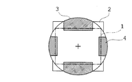
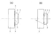
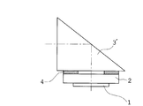
- the optical members 3 adjacent to the cover glass 2 provided in front of the image area 1 satisfy the conditional expressions (1) and (2) as shown in FIG.
- the light shielding region 4 is provided by vapor deposition. Flare is prevented by appropriately blocking out-of-field light by the light shielding region 4.
- a 1 to a 4 in the conditional expression (2) are illustrated in FIG.
- the required shape of the light shielding region can be set by obtaining the vertical opposite side, the horizontal opposite side, and the diagonal on the basis of the conditional expression (2).
- the light shielding area length a is less than a 1 , the light entering from the object side and passing through the transmission area of the optical member and entering the image area of the image sensor is scattered by the light shielding area, and the light entering the light receiving portion is reduced and darkened. End up.
- the light shielding area length a exceeds a 2 ′, light that enters from the object side and passes through the transmission area of the optical member is reflected by the side surface of the cover glass and enters the image area and appears as flare.
- the following conditional expression (1 ′) is satisfied instead of conditional expression (1). 0.85 ⁇ a / IH ⁇ 1.2 (1 ′)
- the following conditional expression (1 ′′) is satisfied. 0.9 ⁇ a / IH ⁇ 1.1 (1 ”)
- the light-shielding region is configured so that at least one boundary portion between the image area of the imaging element and the outside of the image area can be confirmed from the object side.
- the centering performance can be improved.
- the light shielding region is configured so that one or more corners in the boundary portion can be confirmed.
- centering can be performed based on that portion.
- the imaging apparatus is preferably configured so that the light-shielding region can confirm two or more adjacent sides on the boundary.
- centering can be performed based on the two pieces.
- the light shielding area is configured such that the side of the optical member has a transmission area.
- the light-shielding area is shaped so that the edge side of the optical member has a transmission area, the UV transmission area can be increased and the adhesion effect can be enhanced.
- the outer diameter of the light shielding area is larger than the outer diameter of the cover glass.
- the light shielding film in the light shielding region has a thickness in the range of 0.1 ⁇ m to 10 ⁇ m. This is because the necessary light-shielding performance may be obtained.
- the light shielding region is formed of a light shielding film having a transmittance of 5% or less in a wavelength region of 350 to 780 nm.
- a light shielding film having an extremely low transmittance over a wide wavelength range is used, flare can be reliably prevented.
- a material having a high ultraviolet transmittance may be used in order to further enhance the UV adhesive effect.
- an optical member having a transmittance in the wavelength region of 350 to 780 nm of 90% or more it is preferable to use. Since unnecessary light is excluded by the light shielding region, an optical member having high transmittance can be used without excluding a specific wavelength region.
- the light shielding region is formed on the optical member by vapor deposition or printing.
- the imaging device of the present invention is particularly useful for such a configuration.
- the optical member and the cover glass are bonded with a UV adhesive.
- the imaging device of the present invention is particularly useful for such a configuration.
- the imaging apparatus preferably forms a metal film that reduces one or more thin surface reflectances on the surface of the light shielding region. In this way, the reflected light reflected by the light shielding region can be reduced.
- a metal film for reducing the surface reflectance is formed in a transmission region other than the light shielding region. In this way, it is possible to prevent the reflected light from the image area from being reflected. In addition, since the metal film can be formed simultaneously without distinguishing between the light shielding region and the transmission region, the metal film forming operation becomes extremely easy.
- the imaging apparatus according to the first embodiment is deposited on the optical member 3 adjacent to the cover glass 2 provided in front of the image area 1 in accordance with the shape of the image area 1 of the imaging element.
- the light shielding region 4 is formed.
- the surface of the optical member 3 on which the light shielding region 4 is formed and the cover glass 2 are centered and bonded using a UV adhesive 5.
- the image area 1 is an octagon
- the optical member 3 is a circular example
- the outer diameter of the light shielding region 4 is the same as the outer diameter of the optical member 3
- the inner diameter is It is an octagon that satisfies the conditional expressions (1) and (2) and corresponds to the shape of the image area 1.
- the required light shielding area diameter can be set by obtaining the vertical opposite side, the horizontal opposite side, and the diagonal so that the light shielding area length a shown in FIG. 1 satisfies the conditional expressions (1) and (2).
- the light shielding region 4 for preventing flare does not emit the normal light beam entering the image area 1, and flare light is reflected by the side surface of the cover glass 2. Does not enter the image area 1, and as a result, flare can be effectively prevented. Numerical examples of the present embodiment are shown below.
- the light shielding region length a may be larger than the outer periphery of the optical member 3, the light shielding region 4 is not necessarily formed continuously on the outer peripheral portion of the optical member 3 as shown in the following embodiments. Good. That is, even if there is a portion where the light shielding region 4 does not exist in the optical member 3, the conditional expressions (1) and (2) may be satisfied.
- the shape of the light-shielding region 4 will be mainly described.
- the configuration of the imaging device is the same as that of the first embodiment. Note that the value of a obtained by the conditional expressions (1) and (2) that determine the shape of the light shielding region 4 is determined by various parameters in addition to the shape of the image area 1.
- the light shielding region 4 has a shape in which four corners are cut in correspondence with the shape of the image area 1 with respect to the light shielding region of the first embodiment.
- the light shielding area length a only needs to satisfy the conditional expressions (1) and (2). Therefore, a satisfying the conditional expressions (1) and (2) is optical depending on the shape of the image area 1 and the cover glass shape. When it is larger than the outer diameter of the member 3, a light shielding region is not necessary on the optical member for that portion.
- the imaging apparatus of the second embodiment by cutting the four corners of the light shielding region 4 in this way, the boundary between the image area 1 and the outside of the image area can be confirmed from the object side through the transmission region of the optical member 3. As a result, the centering performance can be improved.
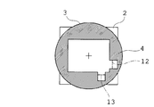
- the light shielding region 4 has a shape in which a part thereof is cut in correspondence with the corner portion 11 of the image area 1 of the image pickup device. And the corner
- the light shielding region 4 can confirm a part of two adjacent sides 12 and 13 of the boundary portion of the image area 1 of the image pickup device through the transmission region of the optical member 3.
- the shape is cut like this.
- the centering can be performed based on the two pieces.
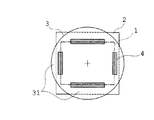
- the light-shielding region 4 is cut at the four corners corresponding to the shape of the image area 1 with respect to the light-shielding region of Example 1, and the optical member 3
- the side edge 31 side has a shape having a transmission region. According to the imaging apparatus of the fifth embodiment configured as described above, when the cover glass 2 and the optical member 3 are bonded with the UV adhesive, the UV transmission region is increased and the bonding effect can be enhanced.
- the light shielding region length a of the light shielding region 4 may be increased within a range satisfying the conditional expressions (1) and (2) to have a curved shape. If the shape of the light-shielding region 4 is further reduced as in the imaging device of the modification, the UV transmission region can be further increased and the adhesion effect can be further enhanced.
- a thermosetting adhesive may be used as the adhesive.
- the outer diameter of the light shielding region 4 is larger than the outer diameter of the cover glass 2 as shown in FIG. To be. If the outer diameter of the light shielding region 4 is smaller than the outer diameter of the cover glass 2, light is incident on the cover glass 2 through the outside of the light shielding region 4 as shown in FIG. I can't plan.
- the imaging apparatus of Example 6 shows an example in which a prism 3 'is used as an optical member. Except for the prism 3 'as the optical member, the shape of the light-shielding region 4 can be the same as in the above embodiments.
- a metal film coating method for reducing the surface reflectance to the transmission region of the optical member 3 used in the imaging apparatus of the present invention will be described based on FIG. This will be described in comparison with FIG.
- the optical member 3 when an antireflection coating is applied to a transmission region for an optical member having a light shielding region, as shown in FIG. 11, the optical member 3 is set on a Yatoi 6 having a shape just covering the light shielding region 4, and the transmission region Only a coating of a metal film for reducing the surface reflectance for preventing reflection is applied.
- a coating of a metal film for reducing the surface reflectance for preventing reflection is applied.
- the antireflection coating since the antireflection coating is not applied to the light shielding region, the reflectance is high in the light shielding region, which may cause flare in some cases.
- the yatoy 6 is hardly blocked by the light shielding region 4 formed in the optical member 3 in the imaging apparatus of each of the above embodiments.
- the transmissive area and the light-shielding area of the optical member 3 are simultaneously coated with a metal thin film that reduces the same surface reflectance.
- the metal film can be formed at the same time without distinguishing between the light shielding region and the transmission region. Therefore, the metal film can be formed very easily and the light shielding can be performed. Since the surface reflectance of the region and the transmission region is reduced, it is possible to prevent the reflected light from the image area from being reflected.
- the light shielding region may be provided on the cover glass side.
- the light shielding region can be applied even when it is formed of a thin metal plate.
- the thickness of the metal thin plate is about 10 to 30 ⁇ m, and may be configured independently of the optical member or the cover glass, or the metal thin plate may be bonded to the optical member in advance.
- the image pickup apparatus of the present invention can effectively prevent flare, improve the centering accuracy of the image area of the image pickup element and the light shielding area of the optical member, and further, UV irradiation curable bonding for bonding the optical member and the cover glass.
- an agent since the adhesion is reliably performed with a light shielding area as a minimum necessary, it can be used as an imaging device for various purposes.
Abstract
An imaging device has a light shielding region between a cover glass of an imaging element and an optical member arranged next to the cover glass, wherein the light shielding region satisfies the following conditional expressions (1) and (2).
0.3 ≤ a/IH ≤ 1.5 ...(1), and
a1 ≤ a ≤ a2' ...(2),
where: a1 = IH − Dtanθ1; a2' is the minimum of a2, a3 and a4 (a2 = 2b − IH − Dtanθ2, a3 = b − (D/2) × tanθ3, and a4 = b − X); a is the length of the light shielding region; IH is the maximum image height in a direction along a; D is the thickness of the cover glass; θ1 is an angle formed with the optical axis by a light beam, among light beams which directly enter positions at the maximum image height in the imaging element, that comes at the maximum light beam height at the light shielding region; b is a distance from the central axis of the cover glass to either one of the side surfaces of the cover glass in the direction along a; θ2 is an angle formed with the optical axis by a light beam, among light beams which are reflected by the side surface of the cover glass and directly enter positions at the maximum image height in the imaging element, that comes at the maximum light beam height at the light shielding region; θ3 is an angle formed with the optical axis by a light beam, among light beams which enter the central portion of the side surface of the cover glass in the direction along a, that comes at the maximum light beam height at the light shielding region; and X is the height of a burr at each of the side surface of a cover glass object in the direction along a.
Description
本発明は、フレア防止のために撮像素子と撮像素子に隣接する光学部材との間に遮光領域を設けた撮像装置に関するものである。
The present invention relates to an image pickup apparatus in which a light shielding region is provided between an image pickup element and an optical member adjacent to the image pickup element in order to prevent flare.
撮像装置においてフレア防止のために、撮像素子近傍に遮光部材が設けられているものがある。例えば、特許文献1には、光学ガラスとセンサチップとの間に絞り部材を備えている撮像モジュールにおいて、透光性部材のガラスに蒸着により絞りが設けられているものが示されている。
Some image pickup devices are provided with a light shielding member in the vicinity of the image pickup element to prevent flare. For example, Patent Document 1 discloses an imaging module having a diaphragm member between an optical glass and a sensor chip, in which a diaphragm is provided by vapor deposition on the glass of a light-transmitting member.
また、特許文献2には、カバーガラスと固体撮像素子との間に遮光領域が設けられた電子内視鏡用撮像素子パッケージが示されている。
Patent Document 2 discloses an image sensor package for an electronic endoscope in which a light shielding region is provided between a cover glass and a solid-state image sensor.
しかしながら、これらの先行例には以下のような課題があった。
特許文献1や特許文献2では、絞り開口エリアについてイメージエリアの形状やカバーガラスの大きさなどを考慮した上での具体的な条件の検討がなされていないため、実際にフレア防止のために撮像素子近傍に遮光部材を設けようとすると、どのような範囲に遮光領域を設ければよいのかが明らかでない。遮光領域は各種条件を考慮して適切な形状に設けられていないとフレア防止効果が十分に発揮されないないので、各種条件を考慮することは非常に重要なことである。 However, these prior examples have the following problems.
InPatent Document 1 and Patent Document 2, no specific conditions are considered for the aperture area in consideration of the shape of the image area and the size of the cover glass. If a light shielding member is provided in the vicinity of the element, it is not clear in what range the light shielding region should be provided. Since the flare prevention effect cannot be fully exhibited unless the light shielding region is provided in an appropriate shape in consideration of various conditions, it is very important to consider various conditions.
特許文献1や特許文献2では、絞り開口エリアについてイメージエリアの形状やカバーガラスの大きさなどを考慮した上での具体的な条件の検討がなされていないため、実際にフレア防止のために撮像素子近傍に遮光部材を設けようとすると、どのような範囲に遮光領域を設ければよいのかが明らかでない。遮光領域は各種条件を考慮して適切な形状に設けられていないとフレア防止効果が十分に発揮されないないので、各種条件を考慮することは非常に重要なことである。 However, these prior examples have the following problems.
In
また、遮光領域により撮像素子のイメージエリアとイメージエリア外との境界部が隠されてしまうと光学系光軸と撮像素子のイメージエリアの芯を合わせる芯出し作業が困難となり、精度も悪くなってしまうが、この点について特許文献1や特許文献2は何ら検討されていない。
In addition, if the boundary between the image area of the image sensor and the outside of the image area is hidden by the light-shielding area, it is difficult to align the optical system optical axis and the image area of the image sensor. However, Patent Literature 1 and Patent Literature 2 are not studied at all in this regard.
さらに、遮光領域を設けた光学部材と撮像素子のカバーガラスとをUV接着剤により接着する場合、遮光領域が必要以上に広いとUV透過領域が狭くなるため十分な接着効果を得ることができないという問題もある。
Furthermore, when the optical member provided with the light shielding region and the cover glass of the image pickup device are bonded with a UV adhesive, if the light shielding region is larger than necessary, the UV transmission region becomes narrow, so that a sufficient bonding effect cannot be obtained. There is also a problem.
本発明は、上述した事情に鑑みてなされたものであって、フレアを効果的に防止できるとともに、光学部材と撮像素子のイメージエリアの芯出し精度と作業効率を上げ、さらに光学部材とカバーガラスの接着にUV照射硬化型接着剤を使用する場合、遮光領域を必要最小限として接着が確実に行われるようにした撮像装置を提供することを目的とする。
The present invention has been made in view of the above-described circumstances, and can effectively prevent flare, increase the alignment accuracy and work efficiency of the image area of the optical member and the image sensor, and further, the optical member and the cover glass. An object of the present invention is to provide an image pickup apparatus in which, when a UV irradiation curable adhesive is used for adhesion, the adhesion is surely performed with a light shielding area as a minimum necessary.
上記課題を解決するために、本発明に係る撮像装置は、撮像素子のカバーガラスと前記カバーガラスに隣接して配置される光学部材の間に遮光領域を有する撮像装置であって、前記遮光領域は次の条件式(1)及び(2)を満足することを特徴とする。
0.3≦a/IH≦1.5 ・・・・・・(1)
a1≦a≦a2’ ・・・・・・(2)
ただし、
a1=IH-Dtanθ1、a2’は下記a2,a3,a4のうちの最小値である。
a2=2b-IH-Dtanθ2
a3=b-(D/2)×tanθ3
a4=b-X
なお、aは前記撮像素子の光軸から前記遮光領域までの距離、IHは前記撮像素子の光軸から前記遮光領域までの距離がaとなる、該撮像素子の光軸から該遮光領域に向けた所定の方向における最大像高、Dは前記カバーガラスの厚さ、θ1は前記撮像素子の前記最大像高位置に直接入射する光線のうち前記遮光領域の位置における最大光線高である光線が光軸となす角度、bは前記カバーガラスの中心軸からカバーガラスの側面までの前記撮像素子の光軸から前記遮光領域までの距離がaとなる、該撮像素子の光軸から該遮光領域に向けた所定の方向における距離、θ2は前記カバーガラスの側面で反射して前記最大像高位置に直接入射する光線のうち前記遮光領域の位置における最大光線高である光線が光軸となす角度、θ3は前記撮像素子の光軸から前記遮光領域までの距離がaとなる、該撮像素子の光軸から該遮光領域に向けた所定の方向において前記カバーガラスの側面の中央部分に入射する光線のうち前記遮光領域の位置における最大光線高である光線が光軸となす角度、Xは前記撮像素子の光軸から前記遮光領域までの距離がaとなる、該撮像素子の光軸から該遮光領域に向けた所定の方向における前記カバーガラスの物体側面のバリの高さである。 In order to solve the above problems, an imaging device according to the present invention is an imaging device having a light shielding region between a cover glass of an imaging element and an optical member disposed adjacent to the cover glass, and the light shielding region. Satisfies the following conditional expressions (1) and (2).
0.3 ≦ a / IH ≦ 1.5 (1)
a 1 ≦ a ≦ a 2 ′ (2)
However,
a 1 = IH−Dtan θ 1 , a 2 ′ is the minimum value of the following a 2 , a 3 , and a 4 .
a 2 = 2b-IH-Dtanθ 2
a 3 = b− (D / 2) × tan θ 3
a 4 = b−X
Here, a is a distance from the optical axis of the image sensor to the light shielding area, and IH is a distance from the optical axis of the image sensor to the light shielding area, from the optical axis of the image sensor to the light shielding area. The maximum image height in a predetermined direction, D is the thickness of the cover glass, and θ 1 is a light beam having the maximum light beam height at the position of the light shielding region among light beams directly incident on the maximum image height position of the image sensor. The angle formed by the optical axis, b is the distance from the optical axis of the image sensor to the light shielding region from the central axis of the cover glass to the side surface of the cover glass, and is from the optical axis of the image sensor to the light shielding region. A distance in a predetermined direction directed, θ 2 is an angle formed by a light beam that is reflected by the side surface of the cover glass and directly incident on the maximum image height position and that has the maximum light beam height at the position of the light shielding region with the optical axis , theta 3 is the image sensor The position of the light shielding region among the light rays incident on the central portion of the side surface of the cover glass in a predetermined direction from the optical axis of the image sensor toward the light shielding region, where the distance from the optical axis to the light shielding region is a. The angle formed by the light beam having the maximum light beam height with respect to the optical axis, X is a predetermined direction from the optical axis of the image sensor to the light shielding region, where the distance from the optical axis of the image sensor to the light shielding region is a. The height of the burrs on the object side surface of the cover glass.
また、本発明に係る撮像装置においては、前記遮光領域は、前記撮像素子のイメージエリアとイメージエリア外との境界部の一箇所以上を、物体側から確認できるように構成されていることが好ましい。
In the image pickup apparatus according to the present invention, it is preferable that the light shielding region is configured so that one or more boundary portions between the image area and the outside of the image area of the image sensor can be confirmed from the object side. .
また、本発明に係る撮像装置においては、前記遮光領域は、前記境界部における一箇所以上の角部を確認できるように構成されていることが好ましい。
Further, in the imaging apparatus according to the present invention, it is preferable that the light shielding region is configured so that one or more corners in the boundary portion can be confirmed.
また、本発明に係る撮像装置においては、前記遮光領域は、前記境界部における隣り合う二辺以上の辺部を確認できるように構成されていることが好ましい。
Further, in the imaging apparatus according to the present invention, it is preferable that the light shielding region is configured so that two or more side portions adjacent to each other in the boundary portion can be confirmed.
また、本発明に係る撮像装置においては、前記遮光領域は、前記光学部材の辺縁部側が透過領域を有するように構成されていることが好ましい。
Further, in the imaging apparatus according to the present invention, it is preferable that the light shielding region is configured such that a side of the optical member has a transmission region.
また、本発明に係る撮像装置においては、前記遮光領域の外径は、前記カバーガラスの外径より大きいことが好ましい。
In the imaging apparatus according to the present invention, it is preferable that an outer diameter of the light shielding region is larger than an outer diameter of the cover glass.
また、本発明に係る撮像装置においては、前記遮光領域は、前記光学部材に蒸着又は印刷により形成されていることが好ましい。
In the imaging device according to the present invention, it is preferable that the light shielding region is formed on the optical member by vapor deposition or printing.
また、本発明に係る撮像装置においては、前記光学部材と前記カバーガラスはUV接着剤で接着されていることが好ましい。
In the imaging apparatus according to the present invention, it is preferable that the optical member and the cover glass are bonded with a UV adhesive.
また、本発明に係る撮像装置においては、前記遮光領域の表面上に一層以上の表面反射率を低減させる金属膜を形成することが好ましい。
In the imaging apparatus according to the present invention, it is preferable to form a metal film that reduces one or more surface reflectances on the surface of the light shielding region.
また、本発明に係る撮像装置においては、前記表面反射率を低減させる金属膜を前記遮光領域以外の透過領域にも形成することが好ましい。
In the imaging apparatus according to the present invention, it is preferable that a metal film for reducing the surface reflectance is formed in a transmission region other than the light shielding region.
本発明の撮像装置によれば、フレアを効果的に防止できるとともに、光学部材と撮像素子のイメージエリアの芯出し精度と作業効率を上げ、さらに遮光領域を必要最小限として光学部材とカバーガラスのUV接着剤による接着が確実に行われるようにすることができる。
According to the image pickup apparatus of the present invention, flare can be effectively prevented, the centering accuracy and work efficiency of the image area of the optical member and the image sensor are increased, and the light shielding area is minimized and the optical member and the cover glass Adhesion by the UV adhesive can be ensured.
実施例の説明に先立ち、本発明に係る撮像装置の作用効果について説明する。
本発明に係る撮像装置は、撮像素子のカバーガラスとカバーガラスに隣接して配置される光学部材の間に遮光領域を有する撮像装置であって、遮光領域は次の条件式(1)及び(2)を満足することを特徴とする。
0.3≦a/IH≦1.5 ・・・・・・(1)
a1≦a≦a2’ ・・・・・・(2)
ただし、
a1=IH-Dtanθ1、a2’は下記a2,a3,a4のうちの最小値である。
a2=2b-IH-Dtanθ2
a3=b-(D/2)×tanθ3
a4=b-X
なお、aは撮像素子の光軸から遮光領域までの距離(遮光領域長)、IHは撮像素子の光軸から遮光領域までの距離がaとなる、該撮像素子の光軸から該遮光領域に向けた所定の方向における最大像高、Dはカバーガラスの厚さ、θ1は撮像素子の最大像高位置に直接入射する光線のうち遮光領域の位置における最大光線高である光線が光軸となす角度、bはカバーガラスの中心軸からカバーガラスの側面までの、撮像素子の光軸から遮光領域までの距離がaとなる、該撮像素子の光軸から該遮光領域に向けた所定の方向における距離、θ2はカバーガラスの側面で反射して最大像高位置に直接入射する光線のうち遮光領域の位置における最大光線高である光線が光軸となす角度、θ3は撮像素子の光軸から遮光領域までの距離がaとなる、該撮像素子の光軸から該遮光領域に向けた所定の方向においてカバーガラスの側面の中央部分に入射する光線のうち遮光領域の位置における最大光線高である光線が光軸となす角度、Xは撮像素子の光軸から遮光領域までの距離がaとなる、該撮像素子の光軸から該遮光領域に向けた所定の方向におけるカバーガラスの物体側面のバリの高さである。 Prior to the description of the embodiments, the operational effects of the imaging apparatus according to the present invention will be described.
An imaging device according to the present invention is an imaging device having a light shielding region between a cover glass of an image sensor and an optical member arranged adjacent to the cover glass, and the light shielding region is defined by the following conditional expressions (1) and ( 2) is satisfied.
0.3 ≦ a / IH ≦ 1.5 (1)
a 1 ≦ a ≦ a 2 ′ (2)
However,
a 1 = IH−Dtan θ 1 , a 2 ′ is the minimum value of the following a 2 , a 3 , and a 4 .
a 2 = 2b-IH-Dtanθ 2
a 3 = b− (D / 2) × tan θ 3
a 4 = b−X
Here, a is the distance from the optical axis of the image sensor to the light shielding area (light shielding area length), IH is the distance from the optical axis of the image sensor to the light shielding area, and a distance from the optical axis of the image sensor to the light shielding area. The maximum image height in a predetermined direction directed, D is the thickness of the cover glass, θ 1 is a light beam having the maximum light beam height at the position of the light shielding region among the light beams directly incident on the maximum image height position of the image sensor. The angle formed by b is a predetermined direction from the optical axis of the image sensor to the light shielding region, where the distance from the optical axis of the image sensor to the light shielding region is a from the central axis of the cover glass to the side surface of the cover glass. , Θ 2 is the angle between the light beam reflected from the side surface of the cover glass and directly incident on the maximum image height position, and the light beam with the maximum light beam height at the position of the light shielding area, and θ 3 is the light from the image sensor The distance from the axis to the light shielding area is a. Of the light rays incident on the central portion of the side surface of the cover glass in a predetermined direction from the optical axis of the element toward the light shielding region, an angle formed by the light beam having the maximum light beam height at the position of the light shielding region with the optical axis, X is an image sensor The height of the burrs on the object side surface of the cover glass in a predetermined direction from the optical axis of the image sensor to the light shielding region, where the distance from the optical axis to the light shielding region is a.
撮像素子のイメージエリアの形状に対応させて、例えば、図1に示すようにイメージエリア1の前に設けられるカバーガラス2に隣接する光学部材3に、条件式(1)及び(2)を満足するように蒸着により遮光領域4が設けられる。遮光領域4により視野外光が適切に遮断されることによってフレアが防止される。
In accordance with the shape of the image area of the image sensor, for example, the optical members 3 adjacent to the cover glass 2 provided in front of the image area 1 satisfy the conditional expressions (1) and (2) as shown in FIG. Thus, the light shielding region 4 is provided by vapor deposition. Flare is prevented by appropriately blocking out-of-field light by the light shielding region 4.
ここで、条件式(2)のa1~a4を図示すると図2の通りである。条件式(2)に基づき縦対辺、横対辺、対角をそれぞれ求めることで必要な遮光領域の形状を設定することができる。
Here, a 1 to a 4 in the conditional expression (2) are illustrated in FIG. The required shape of the light shielding region can be set by obtaining the vertical opposite side, the horizontal opposite side, and the diagonal on the basis of the conditional expression (2).
遮光領域長aがa1を下回ると、物体側から入射し、光学部材の透過領域を通って撮像素子のイメージエリアに入る光線を遮光領域がけってしまい受光部に入る光が減って暗くなってしまう。また遮光領域長aがa2’を上回ると、物体側から入射し、光学部材の透過領域を通った光がカバーガラス側面で反射してイメージエリアに入りフレアとして現れる。
また、条件式(1)に代えて、以下の条件式(1’)を満足すると好ましい。
0.85≦a/IH≦1.2 ・・・・・・(1’)
さらに、以下の条件式(1”)を満足すると一層好ましい。
0.9≦a/IH≦1.1 ・・・・・・(1”) When the light shielding area length a is less than a 1 , the light entering from the object side and passing through the transmission area of the optical member and entering the image area of the image sensor is scattered by the light shielding area, and the light entering the light receiving portion is reduced and darkened. End up. When the light shielding area length a exceeds a 2 ′, light that enters from the object side and passes through the transmission area of the optical member is reflected by the side surface of the cover glass and enters the image area and appears as flare.
Moreover, it is preferable that the following conditional expression (1 ′) is satisfied instead of conditional expression (1).
0.85 ≦ a / IH ≦ 1.2 (1 ′)
Furthermore, it is more preferable that the following conditional expression (1 ″) is satisfied.
0.9 ≦ a / IH ≦ 1.1 (1 ”)
また、本発明に係る撮像装置は好ましくは、遮光領域は、撮像素子のイメージエリアとイメージエリア外との境界部の少なくとも一箇所以上を、物体側から確認できるように構成する。
In the imaging apparatus according to the present invention, it is preferable that the light-shielding region is configured so that at least one boundary portion between the image area of the imaging element and the outside of the image area can be confirmed from the object side.
例えば図3に示すように、遮光領域の四隅をカットして物体側からイメージエリアとイメージエリア外との境界部を確認できるようにすれば、芯出し性能を高めることができる。
For example, as shown in FIG. 3, if the four corners of the light shielding area are cut so that the boundary between the image area and the outside of the image area can be confirmed from the object side, the centering performance can be improved.
また、本発明に係る撮像装置は好ましくは、遮光領域は、境界部における一箇所以上の角部を確認できるように構成する。
Further, in the imaging apparatus according to the present invention, preferably, the light shielding region is configured so that one or more corners in the boundary portion can be confirmed.
例えば図4に示すように、角部を一箇所でも確認できるようにすれば、その箇所を基準に芯出しを行うことができる。
For example, as shown in FIG. 4, if one corner can be confirmed, centering can be performed based on that portion.
また、本発明に係る撮像装置は好ましくは、遮光領域は、境界部における隣り合う二辺以上の辺部を確認できるように構成する。
In addition, the imaging apparatus according to the present invention is preferably configured so that the light-shielding region can confirm two or more adjacent sides on the boundary.
例えば図5に示すように、隣り合う二辺を確認できるようにすれば、その二片を基準に芯出しを行うことができる。
For example, as shown in FIG. 5, if two adjacent sides can be confirmed, centering can be performed based on the two pieces.
また、本発明に係る撮像装置は好ましくは、遮光領域は、光学部材の辺縁部側が透過領域を有するように構成する。
Further, in the imaging apparatus according to the present invention, preferably, the light shielding area is configured such that the side of the optical member has a transmission area.
例えば、図6や図7に示すように、遮光領域を、光学部材の辺縁部側が透過領域を有するような形状とすれば、UV透過領域を増やし接着効果を高めることができる。
For example, as shown in FIGS. 6 and 7, if the light-shielding area is shaped so that the edge side of the optical member has a transmission area, the UV transmission area can be increased and the adhesion effect can be enhanced.
また、本発明に係る撮像装置は好ましくは、遮光領域の外径は、カバーガラスの外径より大きくする。
Further, in the imaging apparatus according to the present invention, preferably, the outer diameter of the light shielding area is larger than the outer diameter of the cover glass.
図8(B)に示すように、遮光領域の外径がカバーガラスの外径より小さい場合は、遮光領域の外側を通ってカバーガラスに光が入射してしまいフレア防止が図れない。
As shown in FIG. 8B, when the outer diameter of the light shielding region is smaller than the outer diameter of the cover glass, light enters the cover glass through the outside of the light shielding region, and flare prevention cannot be achieved.
また、本発明に係る撮像装置は好ましくは、遮光領域の遮光膜は0.1μm~10μmの範囲の厚さとする。必要な遮光性能が得られればよいからである。
In the image pickup apparatus according to the present invention, preferably, the light shielding film in the light shielding region has a thickness in the range of 0.1 μm to 10 μm. This is because the necessary light-shielding performance may be obtained.
また、本発明に係る撮像装置は好ましくは、遮光領域は波長領域350~780nmの透過率が5%以下である遮光膜で形成する。広い範囲の波長領域にわたり極めて低い透過率の遮光膜を使用すると、フレアを確実に防止できる。なお、場合によってはUV接着効果をより高めるために紫外線の透過率の高いものを使用してもよい。
In the imaging apparatus according to the present invention, preferably, the light shielding region is formed of a light shielding film having a transmittance of 5% or less in a wavelength region of 350 to 780 nm. When a light shielding film having an extremely low transmittance over a wide wavelength range is used, flare can be reliably prevented. In some cases, a material having a high ultraviolet transmittance may be used in order to further enhance the UV adhesive effect.
また、本発明に係る撮像装置は好ましくは、光学部材は波長領域350~780nmの透過率が90%以上のものを使用する。不要な光は遮光領域により排除されるので光学部材は特定の波長領域を排除することなく透過率の高いものを使用できる。
In the imaging apparatus according to the present invention, it is preferable to use an optical member having a transmittance in the wavelength region of 350 to 780 nm of 90% or more. Since unnecessary light is excluded by the light shielding region, an optical member having high transmittance can be used without excluding a specific wavelength region.
また、本発明に係る撮像装置は好ましくは、遮光領域は、光学部材に蒸着又は印刷により形成されている。本発明の撮像装置はこのような構成のものに特に有用である。
In the image pickup apparatus according to the present invention, preferably, the light shielding region is formed on the optical member by vapor deposition or printing. The imaging device of the present invention is particularly useful for such a configuration.
また、本発明に係る撮像装置は好ましくは、光学部材とカバーガラスはUV接着剤により接着されている。本発明の撮像装置はこのような構成のものに特に有用である。
In the imaging apparatus according to the present invention, preferably, the optical member and the cover glass are bonded with a UV adhesive. The imaging device of the present invention is particularly useful for such a configuration.
また、本発明に係る撮像装置は好ましくは、遮光領域の表面上に一層以上の薄い表面反射率を低減させる金属膜を形成する。このようにすれば、遮光領域で反射される反射光を減らすことができる。
In addition, the imaging apparatus according to the present invention preferably forms a metal film that reduces one or more thin surface reflectances on the surface of the light shielding region. In this way, the reflected light reflected by the light shielding region can be reduced.
また、本発明に係る撮像装置は好ましくは、表面反射率を低減させる金属膜を遮光領域以外の透過領域にも形成する。このようにすれば、イメージエリアからの反射光が反射されることを防止できる。また、遮光領域と透過領域を区別することなく同時に金属膜を形成できるので、金属膜の形成作業が極めて容易となる。
In addition, in the imaging apparatus according to the present invention, it is preferable that a metal film for reducing the surface reflectance is formed in a transmission region other than the light shielding region. In this way, it is possible to prevent the reflected light from the image area from being reflected. In addition, since the metal film can be formed simultaneously without distinguishing between the light shielding region and the transmission region, the metal film forming operation becomes extremely easy.
以下、本発明に係る撮像装置の実施例を図に基づいて説明する。
Hereinafter, an embodiment of an imaging apparatus according to the present invention will be described with reference to the drawings.
実施例1の撮像装置は、図1及び図2に示すように、撮像素子のイメージエリア1の形状に対応させて、イメージエリア1の前に設けられるカバーガラス2に隣接する光学部材3に蒸着により遮光領域4が形成されている。そして、光学部材3の遮光領域4が形成されている側の面とカバーガラス2がUV接着剤5を用いて芯出し接着されている。
As shown in FIGS. 1 and 2, the imaging apparatus according to the first embodiment is deposited on the optical member 3 adjacent to the cover glass 2 provided in front of the image area 1 in accordance with the shape of the image area 1 of the imaging element. Thus, the light shielding region 4 is formed. Then, the surface of the optical member 3 on which the light shielding region 4 is formed and the cover glass 2 are centered and bonded using a UV adhesive 5.
図示した例ではイメージエリア1は八角形をしており、光学部材3は円形の例を示したものであり、遮光領域4の外径は光学部材3の外径と一致しており、内径は条件式(1)及び(2)を満たすとともにイメージエリア1の形状に対応させた八角形となっている。
In the illustrated example, the image area 1 is an octagon, the optical member 3 is a circular example, the outer diameter of the light shielding region 4 is the same as the outer diameter of the optical member 3, and the inner diameter is It is an octagon that satisfies the conditional expressions (1) and (2) and corresponds to the shape of the image area 1.
図1に示す遮光領域長aが条件式(1)及び(2)を満足するように、縦対辺、横対辺、対角をそれぞれ求めることで必要な遮光領域径を設定することができる。このように構成された実施例1の撮像装置によれば、フレアを防止するための遮光領域4がイメージエリア1に入る正規の光線をけらず、またカバーガラス2の側面での反射によるフレア光がイメージエリア1に入らず、結果として効果的にフレアを防止することができる。
以下に本実施例の数値例を示す。 The required light shielding area diameter can be set by obtaining the vertical opposite side, the horizontal opposite side, and the diagonal so that the light shielding area length a shown in FIG. 1 satisfies the conditional expressions (1) and (2). According to the image pickup apparatus of the first embodiment configured as described above, thelight shielding region 4 for preventing flare does not emit the normal light beam entering the image area 1, and flare light is reflected by the side surface of the cover glass 2. Does not enter the image area 1, and as a result, flare can be effectively prevented.
Numerical examples of the present embodiment are shown below.
以下に本実施例の数値例を示す。 The required light shielding area diameter can be set by obtaining the vertical opposite side, the horizontal opposite side, and the diagonal so that the light shielding area length a shown in FIG. 1 satisfies the conditional expressions (1) and (2). According to the image pickup apparatus of the first embodiment configured as described above, the
Numerical examples of the present embodiment are shown below.
数値例1
本数値例は、a2’=a3の例である。
IH=0.66
b=0.76
D=1.00
X=0.05
θ1=0.049rad
θ2=0.155rad
θ3=0.153rad
a1=0.611
a2=0.704
a3=0.683
a4=0.710
a2’=a3=0.683
amax/IH=1.035
amin/IH=0.926 Numerical example 1
This numerical example is an example in which a 2 ′ = a 3 .
IH = 0.66
b = 0.76
D = 1.00
X = 0.05
θ 1 = 0.049rad
θ 2 = 0.155rad
θ 3 = 0.153rad
a 1 = 0.611
a 2 = 0.704
a 3 = 0.683
a 4 = 0.710
a 2 '= a 3 = 0.683
a max / IH = 1.035
a min /IH=0.926
数値例2
本数値例は、a2’=a4の例である。
IH=0.42
b=0.52
D=0.40
X=0.05
θ1=0.033rad
θ2=0.222rad
θ3=0.210rad
a1=0.407
a2=0.530
a3=0.477
a4=0.470
a2’=a4=0.470
amax/IH=1.119
amin/IH=0.969 Numerical example 2
This numerical example is an example where a 2 ′ = a 4 .
IH = 0.42
b = 0.52
D = 0.40
X = 0.05
θ 1 = 0.033rad
θ 2 = 0.222rad
θ 3 = 0.210rad
a 1 = 0.407
a 2 = 0.530
a 3 = 0.477
a 4 = 0.470
a 2 '= a 4 = 0.470
a max /IH=1.119
a min /IH=0.969
数値例3
本数値例は、a2’=a2の例である。
IH=0.998
b=1.098
D=0.90
X=0.05
θ1=0.072rad
θ2=0.225rad
θ3=0.221rad
a1=0.933
a2=0.992
a3=0.997
a4=1.048
a2’=a2=0.992
amax/IH=0.994
amin/IH=0.935 Numerical example 3
This numerical example is an example of a 2 ′ = a 2 .
IH = 0.998
b = 1.098
D = 0.90
X = 0.05
θ 1 = 0.072rad
θ 2 = 0.225rad
θ 3 = 0.221rad
a 1 = 0.933
a 2 = 0.992
a 3 = 0.997
a 4 = 1.048
a 2 '= a 2 = 0.992
a max /IH=0.994
a min /IH=0.935
なお、遮光領域長aは、光学部材3の外周より大きくなる場合もあるので、以下の実施例で示すように遮光領域4は光学部材3の外周部に必ずしも連続して形成されていなくてもよい。すなわち、光学部材3に遮光領域4が存在しない箇所があっても、条件式(1)及び(2)を満足している場合がある。
Since the light shielding region length a may be larger than the outer periphery of the optical member 3, the light shielding region 4 is not necessarily formed continuously on the outer peripheral portion of the optical member 3 as shown in the following embodiments. Good. That is, even if there is a portion where the light shielding region 4 does not exist in the optical member 3, the conditional expressions (1) and (2) may be satisfied.
また、以下の実施例においては遮光領域4の形状を主に説明するが、撮像装置の構成としては上記実施例1と同様である。なお、遮光領域4の形状を決定することとなる条件式(1)及び(2)により求まるaの値は、イメージエリア1の形状の他、各種パラメータにより定まるものである。
In the following embodiments, the shape of the light-shielding region 4 will be mainly described. However, the configuration of the imaging device is the same as that of the first embodiment. Note that the value of a obtained by the conditional expressions (1) and (2) that determine the shape of the light shielding region 4 is determined by various parameters in addition to the shape of the image area 1.
実施例2の撮像装置は、図3に示すように、遮光領域4は上記実施例1の遮光領域に対してイメージエリア1の形状と対応させて四隅がカットされた形状となっている。上記したように遮光領域長aは条件式(1)及び(2)を満足すればよいので、イメージエリア1の形状とカバーガラス形状によっては条件式(1)及び(2)を満たすaが光学部材3の外径より大きい場合は、その部分については光学部材上に遮光領域は不要となる。
実施例2の撮像装置によれば、このように遮光領域4の四隅をカットすることにより、物体側から光学部材3の透過領域を通しイメージエリア1とイメージエリア外との境界を確認できるようにしたので、芯出し性能を高めることができる。 In the image pickup apparatus according to the second embodiment, as illustrated in FIG. 3, thelight shielding region 4 has a shape in which four corners are cut in correspondence with the shape of the image area 1 with respect to the light shielding region of the first embodiment. As described above, the light shielding area length a only needs to satisfy the conditional expressions (1) and (2). Therefore, a satisfying the conditional expressions (1) and (2) is optical depending on the shape of the image area 1 and the cover glass shape. When it is larger than the outer diameter of the member 3, a light shielding region is not necessary on the optical member for that portion.
According to the imaging apparatus of the second embodiment, by cutting the four corners of thelight shielding region 4 in this way, the boundary between the image area 1 and the outside of the image area can be confirmed from the object side through the transmission region of the optical member 3. As a result, the centering performance can be improved.
実施例2の撮像装置によれば、このように遮光領域4の四隅をカットすることにより、物体側から光学部材3の透過領域を通しイメージエリア1とイメージエリア外との境界を確認できるようにしたので、芯出し性能を高めることができる。 In the image pickup apparatus according to the second embodiment, as illustrated in FIG. 3, the
According to the imaging apparatus of the second embodiment, by cutting the four corners of the
実施例3の撮像装置は、図4に示すように、遮光領域4は撮像素子のイメージエリア1の角部11に対応させて一部がカットされた形状となっている。そして、そのカットされた箇所を通し撮像素子のイメージエリア1の角部11を確認できるようになっている。実施例3の撮像装置によれば、図示するように、イメージエリア1の角部11を一箇所であっても確認できるようにしたので、その箇所を基準に芯出しを行うことができる。
In the image pickup apparatus according to the third embodiment, as illustrated in FIG. 4, the light shielding region 4 has a shape in which a part thereof is cut in correspondence with the corner portion 11 of the image area 1 of the image pickup device. And the corner | angular part 11 of the image area 1 of an image pick-up element can be confirmed through the cut location. According to the image pickup apparatus of the third embodiment, as shown in the figure, since the corner 11 of the image area 1 can be confirmed even at one place, centering can be performed based on that place.
実施例4の撮像装置は、図5に示すように、遮光領域4は撮像素子のイメージエリア1の境界部の隣り合う二辺12,13の一部を、光学部材3の透過領域を通して確認できるようにカットされた形状となっている。実施例4の撮像装置によれば、図示するように、隣り合う二辺12,13を確認できるようにしたので、その二片を基準に芯出しを行うことができる。
As shown in FIG. 5, in the image pickup apparatus according to the fourth embodiment, the light shielding region 4 can confirm a part of two adjacent sides 12 and 13 of the boundary portion of the image area 1 of the image pickup device through the transmission region of the optical member 3. The shape is cut like this. According to the image pickup apparatus of the fourth embodiment, as shown in the figure, since the two adjacent sides 12 and 13 can be confirmed, the centering can be performed based on the two pieces.
実施例5の撮像装置は、図6に示すように、遮光領域4は上記実施例1の遮光領域に対してイメージエリア1の形状と対応させて四隅がカットされているとともに、光学部材3の辺縁部31側が透過領域を有するような形状となっている。このように構成された実施例5の撮像装置によれば、カバーガラス2と光学部材3をUV接着剤で接着するに際し、UV透過領域が増えて接着効果を高めることができる。
As shown in FIG. 6, in the imaging device of Example 5, the light-shielding region 4 is cut at the four corners corresponding to the shape of the image area 1 with respect to the light-shielding region of Example 1, and the optical member 3 The side edge 31 side has a shape having a transmission region. According to the imaging apparatus of the fifth embodiment configured as described above, when the cover glass 2 and the optical member 3 are bonded with the UV adhesive, the UV transmission region is increased and the bonding effect can be enhanced.
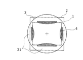
また、本実施例の変形例としては図7に示すように、遮光領域4の遮光領域長aを、条件式(1)及び(2)を満足する範囲で大きくして曲線形状としてもよい。変形例の撮像装置のように、遮光領域4の形状をさらに小さくすれば、UV透過領域がさらに増加し接着効果をより高めることができる。
また、接着剤として熱硬化型接着剤を用いてもよい。 As a modification of the present embodiment, as shown in FIG. 7, the light shielding region length a of thelight shielding region 4 may be increased within a range satisfying the conditional expressions (1) and (2) to have a curved shape. If the shape of the light-shielding region 4 is further reduced as in the imaging device of the modification, the UV transmission region can be further increased and the adhesion effect can be further enhanced.
A thermosetting adhesive may be used as the adhesive.
また、接着剤として熱硬化型接着剤を用いてもよい。 As a modification of the present embodiment, as shown in FIG. 7, the light shielding region length a of the
A thermosetting adhesive may be used as the adhesive.
なお、本実施例のように光学部材3の辺縁部31側を透過領域とする場合は図8(A)に示すように、遮光領域4の外径がカバーガラス2の外径よりも大きくなるようにする。もしも、遮光領域4の外径がカバーガラス2の外径より小さい場合は、同図(B)に示すように、遮光領域4の外側を通ってカバーガラス2に光が入射してしまいフレア防止が図れない。
When the edge 31 side of the optical member 3 is used as the transmission region as in this embodiment, the outer diameter of the light shielding region 4 is larger than the outer diameter of the cover glass 2 as shown in FIG. To be. If the outer diameter of the light shielding region 4 is smaller than the outer diameter of the cover glass 2, light is incident on the cover glass 2 through the outside of the light shielding region 4 as shown in FIG. I can't plan.
実施例6の撮像装置は、図9に示すように、光学部材としてプリズム3’を使用した例を示したものである。光学部材をプリズム3’とした以外は遮光領域4の形状については上記各実施例と同様のものが適用できる。
As shown in FIG. 9, the imaging apparatus of Example 6 shows an example in which a prism 3 'is used as an optical member. Except for the prism 3 'as the optical member, the shape of the light-shielding region 4 can be the same as in the above embodiments.
次に、本発明の実施例7として、本発明の撮像装置で使用する光学部材3の透過領域への表面反射率を低減させる金属膜のコーティング方法を図10に基づき、従来のコーティング方法を示す図11と比較しながら説明する。
Next, as a seventh embodiment of the present invention, a metal film coating method for reducing the surface reflectance to the transmission region of the optical member 3 used in the imaging apparatus of the present invention will be described based on FIG. This will be described in comparison with FIG.
従来、遮光領域を有する光学部材について透過領域に反射防止コートをする場合は、図11に示すように、遮光領域4を丁度カバーするような形状のヤトイ6に光学部材3をセットし、透過領域にのみ反射防止のための表面反射率を低減させる金属膜のコーティングがされるようにしている。このような方法では、透過領域とヤトイを厳密に合わせる必要があり透過領域が複雑な形状であったり、微小で部品精度が高い場合は、コート用ヤトイの作成やヤトイと光学部材との合わせ込みが難しい。また、遮光領域については反射防止コートを行わないので、遮光領域については反射率が高くなり、場合によってはフレアの原因となる。
Conventionally, when an antireflection coating is applied to a transmission region for an optical member having a light shielding region, as shown in FIG. 11, the optical member 3 is set on a Yatoi 6 having a shape just covering the light shielding region 4, and the transmission region Only a coating of a metal film for reducing the surface reflectance for preventing reflection is applied. In such a method, it is necessary to precisely match the transmissive area with the yatoi. If the transmissive area has a complicated shape, or if it is minute and has high component accuracy, it is necessary to create a coat yatoi or align the yatoi with the optical member. Is difficult. In addition, since the antireflection coating is not applied to the light shielding region, the reflectance is high in the light shielding region, which may cause flare in some cases.
そこで、実施例7に係る本発明の撮像装置においては、図10に示すように、ヤトイ6を、上記各実施例の撮像装置における光学部材3に形成されている遮光領域4をほとんど塞がないような形状とし、光学部材3の透過領域と遮光領域に同時に同じ表面反射率を低減させる金属薄膜がコーティングされるようにする。このように構成された実施例7の撮像装置によれば、遮光領域と透過領域を区別することなく同時に金属膜を形成できるので、金属膜の形成作業が極めて容易に行えるようになるとともに、遮光領域及び透過領域の表面反射率が低減するので、イメージエリアからの反射光が反射されることを防止できる。
Therefore, in the imaging apparatus according to the seventh embodiment of the present invention, as shown in FIG. 10, the yatoy 6 is hardly blocked by the light shielding region 4 formed in the optical member 3 in the imaging apparatus of each of the above embodiments. The transmissive area and the light-shielding area of the optical member 3 are simultaneously coated with a metal thin film that reduces the same surface reflectance. According to the imaging apparatus of the seventh embodiment configured as described above, the metal film can be formed at the same time without distinguishing between the light shielding region and the transmission region. Therefore, the metal film can be formed very easily and the light shielding can be performed. Since the surface reflectance of the region and the transmission region is reduced, it is possible to prevent the reflected light from the image area from being reflected.
なお、本発明の撮像装置においては、遮光領域はカバーガラス側に設けてもよい。
また、本発明の撮像装置においては、遮光領域は金属薄板で構成する場合でも適用できる。このとき、金属薄板の厚さは10~30μm程度であり、光学部材やカバーガラスとは独立して構成してもよいし、予め光学部材に金属薄板を接着しておくことも可能である。 In the imaging device of the present invention, the light shielding region may be provided on the cover glass side.
In the imaging apparatus of the present invention, the light shielding region can be applied even when it is formed of a thin metal plate. At this time, the thickness of the metal thin plate is about 10 to 30 μm, and may be configured independently of the optical member or the cover glass, or the metal thin plate may be bonded to the optical member in advance.
本発明の撮像装置は、フレアを効果的に防止でき、また撮像素子のイメージエリアと光学部材の遮光領域の芯出し精度の向上が図れ、さらに光学部材とカバーガラスの接着にUV照射硬化型接着剤を使用する場合、遮光領域を必要最小限として接着が確実に行われるので各種用途の撮像装置として利用可能である。
The image pickup apparatus of the present invention can effectively prevent flare, improve the centering accuracy of the image area of the image pickup element and the light shielding area of the optical member, and further, UV irradiation curable bonding for bonding the optical member and the cover glass. In the case of using an agent, since the adhesion is reliably performed with a light shielding area as a minimum necessary, it can be used as an imaging device for various purposes.
1 イメージエリア
2 カバーガラス
3 光学部材
3’ プリズム
4 遮光領域
5 UV接着剤
6 ヤトイ
11 角部
12,13 辺部
31 辺縁部 DESCRIPTION OFSYMBOLS 1 Image area 2 Cover glass 3 Optical member 3 'Prism 4 Light-shielding area 5 UV adhesive 6 Yatoi 11 Corner | angular part 12, 13 Side part 31 Edge part
2 カバーガラス
3 光学部材
3’ プリズム
4 遮光領域
5 UV接着剤
6 ヤトイ
11 角部
12,13 辺部
31 辺縁部 DESCRIPTION OF
Claims (10)
- 撮像素子のカバーガラスと前記カバーガラスに隣接して配置される光学部材の間に遮光領域を有する撮像装置であって、前記遮光領域は次の条件式(1)及び(2)を満足することを特徴とする撮像装置。
0.3≦a/IH≦1.5 ・・・・・・(1)
a1≦a≦a2’ ・・・・・・(2)
ただし、
a1=IH-Dtanθ1、a2’は下記a2,a3,a4のうちの最小値である。
a2=2b-IH-Dtanθ2
a3=b-(D/2)×tanθ3
a4=b-X
なお、aは前記撮像素子の光軸から前記遮光領域までの距離、IHは前記撮像素子の光軸から前記遮光領域までの距離がaとなる、該撮像素子の光軸から該遮光領域に向けた所定の方向における最大像高、Dは前記カバーガラスの厚さ、θ1は前記撮像素子の前記最大像高位置に直接入射する光線のうち前記遮光領域の位置における最大光線高である光線が光軸となす角度、bは前記カバーガラスの中心軸からカバーガラスの側面までの、前記撮像素子の光軸から前記遮光領域までの距離がaとなる、該撮像素子の光軸から該遮光領域に向けた所定の方向における距離、θ2は前記カバーガラスの側面で反射して前記最大像高位置に直接入射する光線のうち前記遮光領域の位置における最大光線高である光線が光軸となす角度、θ3は前記撮像素子の光軸から前記遮光領域までの距離がaとなる、該撮像素子の光軸から該遮光領域に向けた所定の方向において前記カバーガラスの側面の中央部分に入射する光線のうち前記遮光領域の位置における最大光線高である光線が光軸となす角度、Xは前記撮像素子の光軸から前記遮光領域までの距離がaとなる、該撮像素子の光軸から該遮光領域に向けた所定の方向における前記カバーガラスの物体側面のバリの高さである。 An imaging apparatus having a light shielding region between a cover glass of an imaging element and an optical member disposed adjacent to the cover glass, wherein the light shielding region satisfies the following conditional expressions (1) and (2): An imaging apparatus characterized by the above.
0.3 ≦ a / IH ≦ 1.5 (1)
a 1 ≦ a ≦ a 2 ′ (2)
However,
a 1 = IH−Dtan θ 1 , a 2 ′ is the minimum value of the following a 2 , a 3 , and a 4 .
a 2 = 2b-IH-Dtanθ 2
a 3 = b− (D / 2) × tan θ 3
a 4 = b−X
Here, a is a distance from the optical axis of the image sensor to the light shielding area, and IH is a distance from the optical axis of the image sensor to the light shielding area, from the optical axis of the image sensor to the light shielding area. The maximum image height in a predetermined direction, D is the thickness of the cover glass, and θ 1 is a light beam having the maximum light beam height at the position of the light shielding region among light beams directly incident on the maximum image height position of the image sensor. An angle formed by the optical axis, b is a distance from the optical axis of the image sensor to the light shielding region from the central axis of the cover glass to the side surface of the cover glass, and the light shielding region from the optical axis of the image sensor Is a distance in a predetermined direction toward the light beam, θ 2 is a light beam that is reflected by the side surface of the cover glass and directly enters the maximum image height position, and a light beam having the maximum light beam height at the position of the light shielding region is an optical axis. angle, theta 3 is the imaging element The distance from the optical axis of the image sensor to the light shielding area is a, and out of the light rays incident on the central portion of the side surface of the cover glass in a predetermined direction from the optical axis of the image sensor toward the light shielding area, An angle formed by a light beam having a maximum light ray height at the position and an optical axis, X is a predetermined distance from the optical axis of the image sensor to the light shielding region, where a is a distance from the optical axis of the image sensor to the light shielding region. The height of burrs on the object side surface of the cover glass in the direction. - 前記遮光領域は、前記撮像素子のイメージエリアとイメージエリア外との境界部の一箇所以上を、物体側から確認できるように構成されていることを特徴とする請求項1に記載の撮像装置。 2. The imaging apparatus according to claim 1, wherein the light shielding area is configured so that one or more boundary portions between the image area and the outside of the image area of the imaging element can be confirmed from the object side.
- 前記遮光領域は、前記境界部における一箇所以上の角部を確認できるように構成されていることを特徴とする請求項2に記載の撮像装置。 3. The imaging apparatus according to claim 2, wherein the light shielding region is configured so that one or more corners in the boundary portion can be confirmed.
- 前記遮光領域は、前記境界部における隣り合う二辺以上の辺部を確認できるように構成されていることを特徴とする請求項2に記載の撮像装置。 3. The imaging apparatus according to claim 2, wherein the light-shielding region is configured to be able to check two or more side portions adjacent to each other in the boundary portion.
- 前記遮光領域は、前記光学部材の辺縁部側が透過領域を有するように構成されていることを特徴とする請求項1~4のいずれかに記載の撮像装置。 The imaging apparatus according to any one of claims 1 to 4, wherein the light shielding region is configured such that a side of the optical member has a transmission region.
- 前記遮光領域の外径は、前記カバーガラスの外径より大きいことを特徴とする請求項5に記載の撮像装置。 The imaging apparatus according to claim 5, wherein an outer diameter of the light shielding region is larger than an outer diameter of the cover glass.
- 前記遮光領域は、前記光学部材に蒸着又は印刷により形成されていることを特徴とする請求項1~6のいずれかに記載の撮像装置。 The imaging device according to any one of claims 1 to 6, wherein the light shielding region is formed on the optical member by vapor deposition or printing.
- 前記光学部材と前記カバーガラスはUV接着剤で接着されていることを特徴とする請求項1~6のいずれかに記載の撮像装置。 The imaging apparatus according to any one of claims 1 to 6, wherein the optical member and the cover glass are bonded with a UV adhesive.
- 前記遮光領域の表面上に一層以上の表面反射率を低減させる金属膜を形成したことを特徴とする請求項1~8のいずれかに記載の撮像装置。 9. The imaging apparatus according to claim 1, wherein a metal film that reduces one or more surface reflectances is formed on the surface of the light shielding region.
- 前記表面反射率を低減させる金属膜を前記遮光領域以外の透過領域にも形成したことを特徴とする請求項9に記載の撮像装置。 10. The imaging apparatus according to claim 9, wherein a metal film that reduces the surface reflectance is formed in a transmission region other than the light shielding region.
Priority Applications (4)
| Application Number | Priority Date | Filing Date | Title |
|---|---|---|---|
| CN201080012227.8A CN102356343B (en) | 2009-08-31 | 2010-07-13 | Imaging device |
| JP2011516921A JP4790874B2 (en) | 2009-08-31 | 2010-07-13 | Imaging device |
| EP10811624.5A EP2474848A4 (en) | 2009-08-31 | 2010-07-13 | Imaging device |
| US13/066,713 US8152316B2 (en) | 2009-08-31 | 2011-04-21 | Imaging device |
Applications Claiming Priority (2)
| Application Number | Priority Date | Filing Date | Title |
|---|---|---|---|
| JP2009200091 | 2009-08-31 | ||
| JP2009-200091 | 2009-08-31 |
Related Child Applications (1)
| Application Number | Title | Priority Date | Filing Date |
|---|---|---|---|
| US13/066,713 Continuation US8152316B2 (en) | 2009-08-31 | 2011-04-21 | Imaging device |
Publications (1)
| Publication Number | Publication Date |
|---|---|
| WO2011024573A1 true WO2011024573A1 (en) | 2011-03-03 |
Family
ID=43627684
Family Applications (1)
| Application Number | Title | Priority Date | Filing Date |
|---|---|---|---|
| PCT/JP2010/061829 WO2011024573A1 (en) | 2009-08-31 | 2010-07-13 | Imaging device |
Country Status (5)
| Country | Link |
|---|---|
| US (1) | US8152316B2 (en) |
| EP (1) | EP2474848A4 (en) |
| JP (1) | JP4790874B2 (en) |
| CN (1) | CN102356343B (en) |
| WO (1) | WO2011024573A1 (en) |
Cited By (3)
| Publication number | Priority date | Publication date | Assignee | Title |
|---|---|---|---|---|
| JP2020038402A (en) * | 2017-08-02 | 2020-03-12 | 信泰光學(深セン)有限公司 | Camera device |
| WO2023190837A1 (en) * | 2022-03-31 | 2023-10-05 | 株式会社カネカ | Solid-state imaging device and method for manufacturing same |
| US11852849B2 (en) | 2017-08-02 | 2023-12-26 | Sintai Optical (Shenzhen) Co., Ltd. | Camera device |
Families Citing this family (2)
| Publication number | Priority date | Publication date | Assignee | Title |
|---|---|---|---|---|
| WO2015178134A1 (en) * | 2014-05-21 | 2015-11-26 | オリンパス株式会社 | Image capturing unit and endoscope |
| JP2016012628A (en) * | 2014-06-27 | 2016-01-21 | ソニー株式会社 | Solid-state image pick-up device and electronic apparatus |
Citations (7)
| Publication number | Priority date | Publication date | Assignee | Title |
|---|---|---|---|---|
| JPH0677448A (en) * | 1992-08-25 | 1994-03-18 | Sony Corp | Solid-state image pickup device |
| JPH07311359A (en) * | 1994-05-17 | 1995-11-28 | Olympus Optical Co Ltd | Image pick up optical system |
| JP2006094955A (en) * | 2004-09-28 | 2006-04-13 | Olympus Corp | Imaging apparatus |
| JP2007301227A (en) * | 2006-05-12 | 2007-11-22 | Olympus Medical Systems Corp | Imaging device |
| JP2008034502A (en) * | 2006-07-27 | 2008-02-14 | Epson Toyocom Corp | Solid-state image sensing device cover and solid-state image sensing apparatus |
| WO2008081828A1 (en) * | 2007-01-05 | 2008-07-10 | Nippon Electric Glass Co., Ltd. | Cover glass for solid state imaging device and method for manufacturing the cover glass |
| JP2009066223A (en) * | 2007-09-13 | 2009-04-02 | Olympus Medical Systems Corp | Prism unit for imaging apparatus and imaging unit |
Family Cites Families (11)
| Publication number | Priority date | Publication date | Assignee | Title |
|---|---|---|---|---|
| US5040069A (en) * | 1989-06-16 | 1991-08-13 | Fuji Photo Optical Co., Ltd. | Electronic endoscope with a mask bump bonded to an image pick-up device |
| JP2002334974A (en) * | 2001-05-07 | 2002-11-22 | Nikon Corp | Solid-state imaging device and manufacturing method therefor |
| JP2004031560A (en) * | 2002-06-25 | 2004-01-29 | Nikon Corp | Photoelectric transducer and manufacture thereof |
| JP4358694B2 (en) * | 2004-07-15 | 2009-11-04 | 株式会社リコー | Image input device, digital camera, and portable information terminal device |
| JP2006078517A (en) * | 2004-09-07 | 2006-03-23 | Canon Inc | Imaging module and manufacturing method of imaging module |
| JP2006080597A (en) | 2004-09-07 | 2006-03-23 | Canon Inc | Image pickup module and method of manufacturing the same |
| JP2006128371A (en) * | 2004-10-28 | 2006-05-18 | Fuji Photo Film Co Ltd | Solid state image pickup device and its measuring method |
| JP2007014441A (en) | 2005-07-06 | 2007-01-25 | Pentax Corp | Imaging element package for electronic endoscope |
| JP4794283B2 (en) * | 2005-11-18 | 2011-10-19 | パナソニック株式会社 | Solid-state imaging device |
| KR101058730B1 (en) * | 2007-09-28 | 2011-08-22 | 가시오게산키 가부시키가이샤 | Display element with integral protective plate and display device using same |
| WO2010117115A1 (en) * | 2009-04-09 | 2010-10-14 | Lg Electronics Inc. | Display apparatus |
-
2010
- 2010-07-13 JP JP2011516921A patent/JP4790874B2/en active Active
- 2010-07-13 WO PCT/JP2010/061829 patent/WO2011024573A1/en active Application Filing
- 2010-07-13 CN CN201080012227.8A patent/CN102356343B/en active Active
- 2010-07-13 EP EP10811624.5A patent/EP2474848A4/en not_active Withdrawn
-
2011
- 2011-04-21 US US13/066,713 patent/US8152316B2/en active Active
Patent Citations (7)
| Publication number | Priority date | Publication date | Assignee | Title |
|---|---|---|---|---|
| JPH0677448A (en) * | 1992-08-25 | 1994-03-18 | Sony Corp | Solid-state image pickup device |
| JPH07311359A (en) * | 1994-05-17 | 1995-11-28 | Olympus Optical Co Ltd | Image pick up optical system |
| JP2006094955A (en) * | 2004-09-28 | 2006-04-13 | Olympus Corp | Imaging apparatus |
| JP2007301227A (en) * | 2006-05-12 | 2007-11-22 | Olympus Medical Systems Corp | Imaging device |
| JP2008034502A (en) * | 2006-07-27 | 2008-02-14 | Epson Toyocom Corp | Solid-state image sensing device cover and solid-state image sensing apparatus |
| WO2008081828A1 (en) * | 2007-01-05 | 2008-07-10 | Nippon Electric Glass Co., Ltd. | Cover glass for solid state imaging device and method for manufacturing the cover glass |
| JP2009066223A (en) * | 2007-09-13 | 2009-04-02 | Olympus Medical Systems Corp | Prism unit for imaging apparatus and imaging unit |
Non-Patent Citations (1)
| Title |
|---|
| See also references of EP2474848A4 * |
Cited By (4)
| Publication number | Priority date | Publication date | Assignee | Title |
|---|---|---|---|---|
| JP2020038402A (en) * | 2017-08-02 | 2020-03-12 | 信泰光學(深セン)有限公司 | Camera device |
| JP2022132654A (en) * | 2017-08-02 | 2022-09-08 | 信泰光學(深セン)有限公司 | Camera device |
| US11852849B2 (en) | 2017-08-02 | 2023-12-26 | Sintai Optical (Shenzhen) Co., Ltd. | Camera device |
| WO2023190837A1 (en) * | 2022-03-31 | 2023-10-05 | 株式会社カネカ | Solid-state imaging device and method for manufacturing same |
Also Published As
| Publication number | Publication date |
|---|---|
| JP4790874B2 (en) | 2011-10-12 |
| EP2474848A4 (en) | 2016-03-16 |
| CN102356343B (en) | 2014-06-11 |
| US8152316B2 (en) | 2012-04-10 |
| CN102356343A (en) | 2012-02-15 |
| US20110267696A1 (en) | 2011-11-03 |
| JPWO2011024573A1 (en) | 2013-01-24 |
| EP2474848A1 (en) | 2012-07-11 |
Similar Documents
| Publication | Publication Date | Title |
|---|---|---|
| TWI599801B (en) | Image sensing device and optical film thereof | |
| JP4790874B2 (en) | Imaging device | |
| US9638832B1 (en) | Optical lens | |
| US7554078B2 (en) | Photoelectric encoder | |
| US20080316562A1 (en) | Mems Scanner System and Method | |
| JP6889794B2 (en) | Lens module | |
| JP2006220873A (en) | Optical filter and imaging device | |
| WO2005076049A1 (en) | Chromatic aberration correction imaging optical system | |
| US8902504B2 (en) | Diffractive optical element having a reflective member disposed between different grating wall surfaces thereof, and optical system and optical apparatus having the diffractive optical element | |
| US11469264B2 (en) | Flare-blocking image sensor | |
| WO2012124443A1 (en) | Antireflection tape, wafer-level lens, and imaging device | |
| JP7224620B2 (en) | UV sensor and UV dose measuring device | |
| US20210389510A1 (en) | Spacer | |
| JP2005337827A (en) | Illuminance sensor | |
| JPH09288240A (en) | Visual field direction changing optical system for endoscope | |
| JP2005031024A (en) | Fiber sensor head and fiber-type photoelectric sensor | |
| JP2008077094A (en) | Optical sheet and display device | |
| JP2006228877A (en) | Light receiving device and optical transmitter/receiver module using the same | |
| KR102015840B1 (en) | Camera module | |
| JP6097730B2 (en) | Optical lens | |
| JP2005346004A (en) | Diffractive optical element, multi-layer diffractive optical element and manufacturing method of the diffractive optical element | |
| US11733475B2 (en) | Lens barrel | |
| US11387270B2 (en) | Image sensor package including reflector | |
| JP2017096816A (en) | Object detection device | |
| TWI417643B (en) | Shutter and camera module having same |
Legal Events
| Date | Code | Title | Description |
|---|---|---|---|
| WWE | Wipo information: entry into national phase |
Ref document number: 201080012227.8 Country of ref document: CN |
|
| WWE | Wipo information: entry into national phase |
Ref document number: 2011516921 Country of ref document: JP |
|
| 121 | Ep: the epo has been informed by wipo that ep was designated in this application |
Ref document number: 10811624 Country of ref document: EP Kind code of ref document: A1 |
|
| WWE | Wipo information: entry into national phase |
Ref document number: 2010811624 Country of ref document: EP |
|
| NENP | Non-entry into the national phase |
Ref country code: DE |