WO2011004903A1 - 光拡散板及び光拡散板における光学要素の配列パターンの生成方法 - Google Patents
光拡散板及び光拡散板における光学要素の配列パターンの生成方法 Download PDFInfo
- Publication number
- WO2011004903A1 WO2011004903A1 PCT/JP2010/061739 JP2010061739W WO2011004903A1 WO 2011004903 A1 WO2011004903 A1 WO 2011004903A1 JP 2010061739 W JP2010061739 W JP 2010061739W WO 2011004903 A1 WO2011004903 A1 WO 2011004903A1
- Authority
- WO
- WIPO (PCT)
- Prior art keywords
- base
- pattern
- optical elements
- light
- base patterns
- Prior art date
- Legal status (The legal status is an assumption and is not a legal conclusion. Google has not performed a legal analysis and makes no representation as to the accuracy of the status listed.)
- Ceased
Links
Images








Classifications
-
- G—PHYSICS
- G02—OPTICS
- G02B—OPTICAL ELEMENTS, SYSTEMS OR APPARATUS
- G02B5/00—Optical elements other than lenses
- G02B5/02—Diffusing elements; Afocal elements
- G02B5/0273—Diffusing elements; Afocal elements characterized by the use
- G02B5/0278—Diffusing elements; Afocal elements characterized by the use used in transmission
-
- G—PHYSICS
- G02—OPTICS
- G02B—OPTICAL ELEMENTS, SYSTEMS OR APPARATUS
- G02B5/00—Optical elements other than lenses
- G02B5/02—Diffusing elements; Afocal elements
- G02B5/0205—Diffusing elements; Afocal elements characterised by the diffusing properties
- G02B5/021—Diffusing elements; Afocal elements characterised by the diffusing properties the diffusion taking place at the element's surface, e.g. by means of surface roughening or microprismatic structures
- G02B5/0215—Diffusing elements; Afocal elements characterised by the diffusing properties the diffusion taking place at the element's surface, e.g. by means of surface roughening or microprismatic structures the surface having a regular structure
-
- G—PHYSICS
- G02—OPTICS
- G02F—OPTICAL DEVICES OR ARRANGEMENTS FOR THE CONTROL OF LIGHT BY MODIFICATION OF THE OPTICAL PROPERTIES OF THE MEDIA OF THE ELEMENTS INVOLVED THEREIN; NON-LINEAR OPTICS; FREQUENCY-CHANGING OF LIGHT; OPTICAL LOGIC ELEMENTS; OPTICAL ANALOGUE/DIGITAL CONVERTERS
- G02F1/00—Devices or arrangements for the control of the intensity, colour, phase, polarisation or direction of light arriving from an independent light source, e.g. switching, gating or modulating; Non-linear optics
- G02F1/01—Devices or arrangements for the control of the intensity, colour, phase, polarisation or direction of light arriving from an independent light source, e.g. switching, gating or modulating; Non-linear optics for the control of the intensity, phase, polarisation or colour
- G02F1/13—Devices or arrangements for the control of the intensity, colour, phase, polarisation or direction of light arriving from an independent light source, e.g. switching, gating or modulating; Non-linear optics for the control of the intensity, phase, polarisation or colour based on liquid crystals, e.g. single liquid crystal display cells
- G02F1/133—Constructional arrangements; Operation of liquid crystal cells; Circuit arrangements
- G02F1/1333—Constructional arrangements; Manufacturing methods
- G02F1/1335—Structural association of cells with optical devices, e.g. polarisers or reflectors
- G02F1/1336—Illuminating devices
- G02F1/133602—Direct backlight
- G02F1/133611—Direct backlight including means for improving the brightness uniformity
-
- G—PHYSICS
- G02—OPTICS
- G02F—OPTICAL DEVICES OR ARRANGEMENTS FOR THE CONTROL OF LIGHT BY MODIFICATION OF THE OPTICAL PROPERTIES OF THE MEDIA OF THE ELEMENTS INVOLVED THEREIN; NON-LINEAR OPTICS; FREQUENCY-CHANGING OF LIGHT; OPTICAL LOGIC ELEMENTS; OPTICAL ANALOGUE/DIGITAL CONVERTERS
- G02F1/00—Devices or arrangements for the control of the intensity, colour, phase, polarisation or direction of light arriving from an independent light source, e.g. switching, gating or modulating; Non-linear optics
- G02F1/01—Devices or arrangements for the control of the intensity, colour, phase, polarisation or direction of light arriving from an independent light source, e.g. switching, gating or modulating; Non-linear optics for the control of the intensity, phase, polarisation or colour
- G02F1/13—Devices or arrangements for the control of the intensity, colour, phase, polarisation or direction of light arriving from an independent light source, e.g. switching, gating or modulating; Non-linear optics for the control of the intensity, phase, polarisation or colour based on liquid crystals, e.g. single liquid crystal display cells
- G02F1/133—Constructional arrangements; Operation of liquid crystal cells; Circuit arrangements
- G02F1/1333—Constructional arrangements; Manufacturing methods
- G02F1/1335—Structural association of cells with optical devices, e.g. polarisers or reflectors
- G02F1/1336—Illuminating devices
- G02F1/133602—Direct backlight
- G02F1/133606—Direct backlight including a specially adapted diffusing, scattering or light controlling members
- G02F1/133607—Direct backlight including a specially adapted diffusing, scattering or light controlling members the light controlling member including light directing or refracting elements, e.g. prisms or lenses
Definitions
- the present invention relates to an array pattern generation method, a light diffusing plate, a surface light source device, and a transmissive image display device.
- the backlight unit of a transmissive display such as a liquid crystal display uses a linear light source such as CCFL and a point light source such as an LED, and is converted into a surface light source by diffusing with a light diffusion plate. ing.
- a transmissive display transmissive image display device
- a linear light source such as CCFL
- a point light source such as an LED
- Some optical films used in combination with a light diffusing plate have a periodic structure in which optical elements are juxtaposed, such as a prism sheet.
- a shaped diffusion plate having a periodic structure is used in combination with an LCD panel or an optical film having a periodic structure, interference fringes may occur due to the relationship between the widths (pitch) of the two.
- interference fringes with a period of several millimeters are generated, they are easily recognized by the human eye, and there is a problem that the display quality of the display is remarkably lowered.
- Patent Documents 1 to 3 are known. That is, in the technique described in Japanese Patent Application Laid-Open No.
- Patent Document 1 the first surface structure function having the function of the microlens structure is replaced with the second surface structure function having the characteristic of giving diffused light.
- the surface shape obtained by the modulation is given to the light diffusion plate.
- two-dimensional waviness is formed on the surface of the light diffusion plate.
- Patent Document 2 discloses a technique of repeatedly arranging optical shape groups having unit optical shapes having different widths between adjacent units.
- JP 2009-37984 A discloses a first prism row having a first height, and a second prism row having a second height lower than the first height. And a technique of disposing at least one second prism row between first prism rows adjacent to each other.
- the technique described in Patent Document 1 it is difficult to form a surface shape because the surface of the light diffusing plate has a two-dimensional wavy structure.
- the technique described in Patent Document 2 has a periodic structure with a unit optical shape group as a unit. For example, depending on a liquid crystal panel or an optical sheet combined with a light diffusion plate, interference fringes are generated.
- the first prism row and the second prism row are used. Since the configuration between the first prism rows adjacent to each other is the same, a certain periodicity is obtained. Will have. Therefore, as in the case of Patent Document 2, in order to prevent the occurrence of interference fringes, the method of breaking periodicity is insufficient, and interference fringes may occur.
- the present invention provides a light diffusing plate in which a plurality of optical elements extending in a predetermined direction are formed in parallel to each other, and the light diffusing plate that can more reliably suppress the generation of interference fringes. It is an object of the present invention to provide a method for generating an array pattern of optical elements, a surface light source device using the light diffusion plate, and a transmissive image display device.
- the light diffusing plate according to the present invention is a light diffusing plate capable of emitting light incident from the first surface from the second surface, and has a first direction on at least one of the first and second surfaces.
- a plurality of optical elements extending in the direction are formed, and the plurality of optical elements are arranged side by side in a second direction orthogonal to the first direction, and are optical elements composed of N optical elements continuous in the second direction.
- 100 optical element groups are selected so that combinations of optical elements included in the element groups are different from each other, and the frequency of occurrence of the width in the second direction of each of the 100 optical element groups is set so that N is 8 or more and 14 or less.
- the maximum appearance frequency is 50 times or less.
- the width when a plurality of continuous optical elements are taken out has a distribution, and has a specific length. It will be difficult to concentrate.
- each optical element extends in the first direction and is arranged in the second direction, the plurality of optical elements are parallel to each other. Therefore, it is easy to form an optical element in the light diffusing plate.
- the cross-sectional shape orthogonal to the first direction of the plurality of optical elements is similar. Thereby, it is possible to realize the same optical characteristics in each optical element.
- the array pattern generation method is a method for generating an array pattern of optical elements arranged on a light diffusing plate, wherein the light diffusing plate transmits light incident from a first surface to a second surface.
- a plurality of optical elements extending in at least one of the first and second surfaces extending in the first direction in a second direction orthogonal to the first direction.
- Repeat the alignment process A repeating step for returning, and in each repeating step, a base pattern other than the base pattern selected in the previous step is selected from a plurality of base patterns, and n is randomly selected each time. select.
- the process of arranging one base pattern selected from a plurality of base patterns at a random number selected from an integer of 1 or more is repeated as described above to generate an array pattern.
- the array pattern generated by the array pattern according to the present invention is an array pattern of optical elements extending in the first direction and arranged in parallel in the second direction, the light on which the optical elements are formed In the diffuser plate, the plurality of optical elements are parallel to each other. Therefore, it is easy to form an optical element in the light diffusing plate.
- the array step in the array pattern generation method according to the present invention it is preferable to select one base pattern randomly from a plurality of base patterns.
- the basic unit is repeated with P repetitions (P is an integer of 2 or more) of the arrangement process as a basic unit, and the arrangement process of P times in the basic unit is performed.
- P is an integer of 2 or more
- the base pattern is selected in a predetermined order in the first to p-th arrangement steps (p is an integer of 2 or more and P or less), and in the arrangement steps after the p-th arrangement, the previous arrangement is performed.
- a base pattern other than the base pattern selected in the process is also preferable to randomly select a base pattern other than the base pattern selected in the process from a plurality of base patterns.
- the basic unit is repeated in the repetition process as described above, among the repetitions of the P arrangement processes in the basic unit, in the arrangement process after the p-th, the base pattern is changed to the previous one.
- the base pattern other than the base pattern selected in the array step and the base pattern other than the base pattern selected in the first to p-th array steps may be selected at random.
- the number of base patterns prepared in the preparation step is any of 2 to 4.
- An increase in the plurality of base patterns corresponds to an increase in the plurality of optical elements having different widths. Therefore, the manufacturing cost of the light diffusing plate tends to increase.
- the number of base patterns to be prepared is 2 to 4, it is possible to suppress an increase in manufacturing cost while reducing interference fringes.
- the maximum number (maximum number of juxtapositions) of base patterns arranged in the width direction is an integer of 2 to 4. Is preferred. n corresponds to the maximum juxtaposition number when optical elements corresponding to one base pattern are continuously arranged.
- the second base pattern when the plurality of base patterns are the first to third base patterns, and the widths of the first and third base patterns correspond to the minimum value and the maximum value, respectively, the second base pattern
- the width of the pattern is preferably (M ⁇ 0.6D) or more and (M ⁇ 0.2D) or less or (M + 0.2D) or more and (M + 0.6D) or less.
- the plurality of base patterns are first to fourth base patterns, and the widths of the first and fourth base patterns among the first to fourth base patterns are the minimum value and the maximum value, respectively.
- the width of the second base pattern and the width of the third base pattern are (M ⁇ 0.333D) and (M + 0.667D), respectively, or the width of the second base pattern and the third base pattern.
- the pattern widths are preferably (M ⁇ 0.667D) and (M + 0.333D), respectively.
- the plurality of base patterns are preferably similar to each other. Thereby, optical elements having different widths corresponding to the respective base patterns can have the same optical characteristics.
- the present invention is a light diffusing plate capable of emitting light incident from the first surface from the second surface, and is a plurality of optical elements extending in the first direction and orthogonal to the first direction.
- the plurality of optical elements having different widths in the second direction are formed on at least one of the first and second surfaces, and the plurality of optical elements having different widths are arranged in the array pattern generation method according to the present invention.
- the present invention also relates to a light diffusing plate that is arranged in the second direction in an arrangement pattern of a plurality of optical elements arranged in different widths.
- This light diffusing plate has a plurality of optical elements having different widths, and the plurality of optical elements are arranged in an array state of the base pattern generated by the array pattern generating method according to the present invention. Therefore, even if a light diffusing plate and an optical component having a periodic structure are combined, the generation of interference fringes can be suppressed. Furthermore, since the plurality of optical elements having different widths are arranged in parallel to each other, it is easy to manufacture the light diffusing plate.
- the surface light source device according to the present invention includes the light diffusing plate according to the present invention and a light source unit for supplying light to the first surface of the light diffusing plate. This surface light source device includes a light diffusing plate according to the present invention.
- a transmissive image display device includes a light diffusing plate according to the present invention, a light source unit for supplying light to a first surface of the light diffusing plate, and a light diffusing plate output from the light source unit.
- a transmissive image display unit that is illuminated by the light that has passed and displays an image.
- the transmissive image display unit included in the transmissive image display device has a plurality of pixels for displaying an image, but these pixels are usually arranged at a predetermined pitch. Therefore, the transmissive image display unit has a periodic structure.
- the transmissive image display device the light diffusing plate according to the present invention and the transmissive image display unit having a periodic structure are combined. As described above, since the generation of interference fringes can be suppressed even when combined with an optical component having a periodic structure, an image in which deterioration of display quality is suppressed can be displayed. Further, in the light diffusing plate according to the present invention, since the plurality of optical elements are parallel, it is easy to form the optical elements.
- the light diffusing plate and the transmissive image display device including the light diffusing plate are provided. Easy to manufacture.
- a light diffusing plate in which a plurality of optical elements extending in a predetermined direction are formed in parallel to each other, and the light diffusing plate that can more reliably suppress the generation of interference fringes.
- An optical element array pattern generation method, a surface light source device using the light diffusion plate, and a transmissive image display device can be provided.
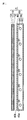
- FIG. 1 is a cross-sectional view schematically showing a configuration of a transmissive image display device to which an embodiment of a light diffusion plate according to the present invention is applied.
- FIG. 2 is a side view of an embodiment of a light diffusing plate according to the present invention.
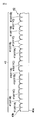
- FIG. 3 is a diagram illustrating a method for evaluating randomness of an optical element array in a light diffusing plate.
- FIG. 4 is a flowchart showing a method for manufacturing a light diffusing plate.
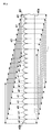
- FIG. 5 is a diagram illustrating a transition state of the base pattern.
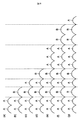
- FIG. 6 is a diagram illustrating an example of an array pattern generation process.
- FIG. 7 is a diagram illustrating another example of the generation process of the array pattern.
- FIG. 1 is a cross-sectional view schematically showing a configuration of a transmissive image display device to which an embodiment of a light diffusion plate according to the present invention is applied.
- FIG. 2 is a side view of an embodiment of a light diffusing plate
- FIG. 8 is a drawing showing one step of the light diffusing plate manufacturing process.
- FIG. 9 is a table showing the array pattern generation conditions and evaluation results of Examples 1 to 15.
- FIG. 10 is a chart showing array pattern generation conditions and evaluation results of Comparative Examples 1 to 6.
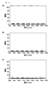
- 11A to 11C are diagrams showing the appearance frequency distributions of Examples 1 to 3, respectively.
- 12A to 12C are diagrams showing the appearance frequency distributions of Examples 4 to 6, respectively.
- FIG. 13A to FIG. 13C are diagrams showing appearance frequency distributions of Examples 7 to 9, respectively.
- FIG. 14 (a) to (c) are diagrams showing the appearance frequency distributions of Examples 10 to 12, respectively.
- FIG. 15 is a drawing showing the appearance frequency distributions of Examples 13 to 15 (a) to (c), respectively.
- 16A to 16C are diagrams showing the appearance frequency distributions of Comparative Examples 1 to 3, respectively.
- 17A to 17C are diagrams showing the appearance frequency distributions of Comparative Examples 4 to 6, respectively.
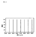
- FIG. 18 is a diagram illustrating an appearance frequency distribution of the sixteenth embodiment.
- FIG. 19 is a drawing showing the appearance frequency distribution of Comparative Example 7.
- FIG. 20 is a diagram for explaining the interference fringe simulation.
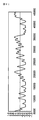
- FIG. 21 is a drawing showing the interference fringe simulation results of Example 16.
- FIG. 22 is a diagram showing an interference fringe simulation result of Comparative Example 7.
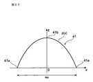
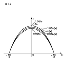
- FIG. 23 is a drawing showing an example of a cross-sectional shape of an optical element.
- FIG. 24 is a diagram illustrating an example of a condition satisfied by a contour line indicating a cross-sectional shape of the optical element.
- FIG. 1 is a cross-sectional view schematically showing a configuration of an embodiment of a transmissive image display device according to the present invention.
- FIG. 1 is an exploded view of a transmissive image display device.
- FIG. 2 is an enlarged view of a light diffusing plate included in the surface light source device included in the transmissive image display device shown in FIG.
- the transmissive image display device 1 includes a transmissive image display unit 10 and a surface light source device 20 as a direct backlight unit arranged on the back side (lower side) of the transmissive image display unit 10. Is done.
- the transmissive image display unit 10 has a plurality of pixels arranged at a predetermined pitch. Examples of the transmissive image display unit 10 include a liquid crystal display panel in which linearly polarizing plates 12 and 13 are disposed on both surfaces of a liquid crystal cell 11. In this case, the transmissive image display device 1 is a liquid crystal display device (or a liquid crystal television).
- the surface light source device 20 includes a light source unit 30 including a plurality of light sources 31 arranged in parallel.
- Each light source 31 is a linear light source 31 extending in a direction orthogonal to the arrangement direction of the plurality of light sources 31, and a straight tube like a fluorescent lamp (cold cathode ray lamp) is exemplified.
- the plurality of light sources 31 are arranged at intervals so that the central axes of the light sources 31 are located in the same plane.
- the light source 31 is linear, but it is also possible to use a point light source 31 such as an LED.
- the plurality of light sources 31 are preferably arranged in a lamp box 32, and the inner surface of the lamp box 32 is preferably formed as a light reflecting surface.
- the surface light source device 20 includes a plate-like light diffusing plate 40 that is disposed apart from the light source 31 on the front side (upper side in FIG. 1) of the light source unit 30, that is, on the transmissive image display unit 10 side. Have.
- a planar view shape of the light diffusing plate 40 for example, a rectangular shape such as a rectangle or a square can be cited.
- the light diffusion plate 40 is made of a transparent material such as a transparent resin or transparent glass.
- polycarbonate resin As transparent resin, polycarbonate resin, ABS resin (acrylonitrile-styrene-butadiene copolymer resin), methacryl resin, MS resin (methyl methacrylate-styrene copolymer resin), polystyrene resin, AS resin (acrylonitrile-styrene copolymer) Examples thereof include polyolefin resins such as coalesced resin), polyethylene, and polypropylene.
- first main surface first surface
- second surface second main surface
- the light diffusing plate 40 is a shaped diffusing plate in which a predetermined shape is shaped on the second main surface 40b.
- FIG. 2 is a side view of the light diffusion plate.
- a plurality of optical elements 41 extending in one direction (first direction) are formed as an uneven structure.
- the extending direction of the optical element 41 is referred to as a y direction (first direction), and the direction orthogonal to the extending direction of the optical element 41 is referred to as an x direction (second direction).
- FIG. 2 shows a side configuration when viewed from the y direction.
- the plurality of optical elements 41 are continuously arranged in parallel in the x direction (second direction) to form an optical element row 42.
- the plurality of optical elements 41 can be arranged such that the ends of the adjacent optical elements 41 overlap in the cross-sectional shape orthogonal to the y direction of each optical element 41.
- Each optical element 41 may be, for example, an optical element 41 such as a lens having a curved cross-sectional outline or a prism having a triangular cross-sectional shape.
- an optical element 41 such as a lens having a curved cross-sectional outline or a prism having a triangular cross-sectional shape.
- a cylindrical lens is exemplified.
- the optical element 41 is not particularly limited as long as it has a shape having optical characteristics such as a diffusion action in the light diffusion plate 40.
- FIG. 2 illustrates the case where each optical element 41 is a cylindrical lens.
- the optical element 41 is a cylindrical lens, and the cross-sectional shapes of the optical elements 41 are described as being similar to each other.
- the light output from the light source 31 is the first main surface 40a that is the surface of the light diffusion plate 40 on the light source 31 side. Incident from.
- the light that has entered the light diffusing plate 40 from the first main surface 40a propagates through the light diffusing plate 40 and is emitted through the optical elements 41 formed on the second main surface 40b.
- the light emission direction differs depending on the difference in the refraction direction according to the emission position. As a result, the light from the light source 31 is diffused by the light diffusion plate 40.
- planar light is formed from the light from the light source 31. That is, planar light can be output from the surface light source device 20 having the light diffusing plate 40, and the transmissive image display device 1 illuminates the transmissive image display unit 10 with the planar light to display an image. It can be displayed.
- the optical element row 42 included in the light diffusion plate 40 will be described in more detail. As shown in FIG. 2, each optical element 41 constituting the optical element array 42 of the light diffusing plate 40 has a plurality of types having different widths (lengths in the x direction).
- each of the optical elements having different widths is represented as an optical element 411A, an optical element 411B, an optical element 411C, an optical element 411D, and the like.
- the optical element row 42 a plurality of optical elements 41 are arranged by randomly selecting at least one of their arrangement order and the consecutive juxtaposition number of the same optical elements 41. That is, the optical element row 42 is a plurality of optical elements 41 having different widths, which are randomized in the x direction and arranged in parallel.
- FIG. 2 an optical element array 42 including three optical elements 411A, 411B, and 411C having different widths is shown.
- FIG. 1 An optical element array 42 including three optical elements 411A, 411B, and 411C having different widths is shown.
- a group (optical element group) of N optical elements 41 (N is an integer of 8 or more and 14 or less) continuous in the x direction is randomly selected, and the total width thereof is measured. This operation is repeated 100 times to obtain the appearance frequency of the total width. However, when repeating 100 times, a group of optical elements 41 each consisting of a combination of different optical elements 41 is selected. Further, the minimum width of the plurality of optical elements 41 constituting the optical element row 42, in other words, 1/100 of the minimum width of the plurality of optical elements 41 is used as the aggregation unit.
- the total width of the N optical elements 41 is rounded off, for example, to less than 1 ⁇ m.
- optical elements 41 are selected, and the total is selected. If the width is measured and the measurement is continued 100 times while shifting one by one, the measurement can be performed 100 times with a combination of different groups of optical elements 41.
- the group of N optical elements 41 is selected for each measurement. However, a group of N optical elements 41 of 100 sets is selected in advance, and a group of N optical elements 41 is selected. Measurements may be performed on each.
- the maximum appearance frequency is 50 times or less, preferably the maximum appearance frequency is 30 times or less. is there.
- the manufacturing method of the light diffusing plate 40 includes an array pattern generating step S10 for generating an array pattern of the optical elements 41 and a light diffusing plate manufacturing step for manufacturing the light diffusing plate 40 based on the array pattern generated in the array pattern generating step S10. S20. Each process S10, S20 is demonstrated. [Sequence pattern generation process] In the array pattern generation step S10, a plurality of base patterns that should correspond to the cross-sectional outlines of the plurality of optical elements 41 having different widths are prepared (preparation step S11). Each base pattern may be designed to have a desired optical characteristic such as a diffusion action.
- one base pattern is randomly selected from a plurality of base patterns having different widths, and n base patterns are continuously arranged in the width direction (arrangement step S12).
- the juxtaposition number n is a number randomly selected from an integer of 1 or more.
- sequence process S12 is repeated sequentially (repetition process S13).
- the juxtaposition number n in the alignment step S12 that is repeatedly performed is selected at random each time.
- a base pattern other than the base pattern selected in the previous round is selected. To do.
- FIG. 5A and 5B are diagrams for explaining the transition states of a plurality of base patterns.
- FIG. 5A shows the transition states of two types of base patterns
- FIG. 5B shows the transition states of three types of base patterns
- FIG. 5C shows transition states of four types of base patterns.
- “A”, “B”, “C”, and “D” represent base patterns having different widths.
- each arrow indicates repetition of the alignment step S12
- an arrow with “x” indicates prohibition of transition. Accordingly, as shown in FIGS.
- the base pattern transitions to a base pattern different from the previous pattern.
- transition is made alternately to the base patterns A and B as indicated by the bold lines.
- 5B and 5C the transition from the base pattern A will be described.
- the base pattern B and C other than the base pattern A are randomly transitioned.
- Arrangement of base patterns having different widths by arranging the base patterns randomly selected for each repeated array process S12 by the number selected for each array process S12 by repeating the above-described array process S12. The state is determined. Since the base patterns having different widths correspond to the optical elements 41, the arrangement pattern of the optical elements 41 is generated by repeating the arrangement step S12. In the light diffusion plate 40 shown in FIG.
- the repetition step S13 can be ended when the total length in the width direction of the arranged base patterns reaches a predetermined length. Examples of the predetermined length include the length of the width in the x direction of the light diffusion plate 40 to be manufactured.
- the random selection of the base pattern and the juxtaposition number in the arranging step S12 can be performed using, for example, a random number.
- the array pattern generation step S10 may be executed using a computer, or may be executed manually by the designer of the light diffusing plate 40. In the above description, the case where one base pattern is randomly selected from a plurality of base patterns in the arranging step S12 has been described.
- the base patterns may be selected in a predetermined order in the repeated arrangement step S12.
- the base pattern makes a fixed transition as illustrated by the bold lines in FIGS. 5B and 5C.
- the case where three types of base patterns (base patterns A, B, and C) are prepared in the preparation step S11 will be specifically described as an example.
- selection is made in the order of base pattern A-base pattern B-base pattern C as illustrated by the bold line in FIG.
- the basic unit for selecting the base pattern A in the first arrangement step S12, the base pattern B in the second arrangement step S12, and the base pattern C in the third arrangement step S12 is used as a repetition unit. By repeating, an array pattern is generated.
- three types of base patterns are prepared has been described as an example, the same can be applied to the case where four types of base patterns (base patterns A to D) are prepared in the preparation step S11.
- base patterns A to D base patterns
- the selection is made in a predetermined order such as alternate selection of two base patterns.
- a method for generating an array pattern will be described more specifically with reference to FIGS. FIG.
- FIG. 6 shows an array pattern generated using base patterns A and B having similar shapes and two widths.
- the maximum number of juxtapositions of the base patterns A and B is three.
- the base pattern A or the base pattern B is selected at random from the base patterns A and B.
- the base pattern A is selected.
- the number of consecutive base patterns A is randomly selected from 1 to 3, and the same number of base patterns A are arranged.
- 2 is selected.
- a base pattern B different from the base pattern A selected immediately before is selected from the base patterns A and B.
- the number of consecutive base patterns B is randomly selected from 1 to 3, and the same number of base patterns B are arranged.
- 1 is selected.
- the base pattern A and the base pattern B are alternately selected, and each time the base pattern is selected, the number of the selected base patterns is set to 1 to 3. Randomly select from our house.
- the numbers of the selected base patterns are 1, 1, 3, 2, 1 respectively.
- the base patterns A and B are alternately selected, and an array pattern is formed by repeating the arrangement of a random number selected from 1 to 3.
- the base patterns A and B are AABABAAABBA ...
- the arrangement pattern arranged in this order is formed.
- FIG. 7 shows generation of an array pattern using base patterns A, B, C, and D having similar widths and four widths.
- the maximum number of juxtapositions when the base patterns A, B, C, and D are arranged is three.
- the base pattern A is selected.
- the number of base patterns A selected at random from 1 to 3 is arranged.
- 2 is selected.
- FIG. 7B one of the base patterns A to D other than the previously selected base pattern A is selected at random.
- the base pattern B is selected.
- the numbers selected at random from 1 to 3 are arranged.
- 1 is selected.
- FIGS. 7C to 7E a base pattern other than the base pattern selected immediately before is selected from the base patterns A to D, and randomly selected from 1 to 3 Arrange the number.
- FIGS. 7C to 7E show a case where the base pattern C, the base pattern D, and the base pattern A are selected in order. Also, in FIGS. 7C to 7E, 3, 1, and 1 are selected as the numbers of the selected base patterns. Hereinafter, similarly, random selection of one base pattern from the base patterns A to D and random selection of the juxtaposition number are repeated to generate an array pattern. As a result, the base patterns A, B, C, D are AABCCCDA ... The arrangement pattern arranged in this order is formed. [Light diffusion plate manufacturing process] In the light diffusing plate manufacturing step S20, the light diffusing plate 40 is manufactured based on the array pattern generated in the array pattern generating step S10.
- FIG. 8 is a drawing showing one step of the manufacturing process of the light diffusing plate.
- the transparent resin prepared as the material of the light diffusing plate 40 is extruded from the die 50, and, for example, is clamped and cooled by three polishing rolls 51, 52, 53 to obtain the light diffusing plate 40.
- the light diffusing plate 40 having the array pattern formed on the surface is prepared by preparing a mold based on the array pattern generated in the array pattern generation step S10 on either surface of the polishing rolls 52 and 53. Obtainable.
- the mold corresponding to the arrangement pattern may be produced using, for example, a byte (tool bit).
- a cutting tool corresponding to each of the plurality of optical elements 41 having different widths is prepared, and the mold is manufactured using these cutting tools. For example, if the width is simply changed, it is possible to change the width by changing the digging depth of a bit having the same shape. However, if it does so, the external shape of the plurality of optical elements 41 to be formed will be different from each other, and the optical characteristics at the time of design may not be obtained. Therefore, as described above, it is preferable to prepare a cutting tool corresponding to each of the plurality of optical elements 41 having different widths and make a mold using these cutting tools.
- one base pattern is selected, for example, at random from base patterns having different widths, and the process of arranging the selected base patterns at random from a predetermined number is repeated, thereby repeating the optical elements 41 having different widths.
- Generate an array pattern of And the light diffusing plate 40 is manufactured based on the arrangement pattern. Therefore, in the manufacturing method described above, it is possible to manufacture the light diffusing plate 40 including the optical element array 42 whose periodicity is greatly reduced.
- the maximum appearance frequency can be set to 50 times or less, preferably 30 times or less in the appearance frequency distribution of the total width.
- one base pattern is randomly selected from a plurality of base patterns for each repeated array step S12 in the array pattern generation method described using FIG. It is more preferable to do.
- the light diffusing plate 40 is applied to the surface light source device 20 and the transmissive image display device 1 in contrast to the case of a shaped light diffusing plate formed with an optical element array having a periodic structure as in the prior art.
- the transmissive image display unit 10 of the transmissive image display device 1 includes a plurality of pixels arranged at a predetermined pitch. Therefore, the transmissive image display unit 10 has a periodic structure. It is known that when a shaped light diffusing plate having a periodic structure is used in combination with the transmissive image display unit 10 having such a periodic structure, interference fringes are generated due to the relationship between the two periodic structures. On the other hand, in the light diffusing plate 40 of this embodiment, the periodicity is significantly reduced in the optical element row 42 or there is almost no periodicity. Specifically, in the light diffusing plate 40, when evaluated by the randomness evaluation method described above, the maximum appearance frequency is 50 times or less.
- the maximum appearance frequency is preferably 30 times or less in the evaluation by the randomness evaluation method. Since the generation of interference fringes can be suppressed in the transmissive image display device 1 including the light diffusing plate 40 as described above, display quality can be improved in the transmissive image display device.
- the pixel size varies depending on the size and resolution, and therefore the period of the periodic structure is different for each different transmissive image display unit 10.
- the light diffusing plate 40 since the total width when a certain number of optical elements 41 are continuously extracted is dispersed without being concentrated on a specific length, it is assumed that they are combined in different transmissive image display units 10. Also, the generation of interference fringes can be suppressed. That is, the light diffusion plate 40 has versatility. Therefore, it is not necessary to design the light diffusing plate 40 for each of the different transmissive image display units 10, so that it is possible to suppress an increase in manufacturing costs of the surface light source device 20 including the light diffusing plate 40 and the transmissive image display device 1. it can.
- the light diffusing plate 40 a plurality of optical elements 41 extending in one direction are arranged in parallel in a direction orthogonal to the extending direction to constitute an optical element row 42. Therefore, the plurality of optical elements 41 are arranged in a parallel pattern.
- the light diffusing plate 40 can be suitably manufactured by an extrusion method as illustrated.
- sequence pattern was formed in the surface can be utilized in the manufacture, it can be said that it is easy to manufacture the light diffusing plate 40, and can be said to be a structure contributing to mass production.
- the surface light source device 20 including the light diffusion plate 40 and the transmissive image display device 1 can be easily manufactured, and the manufacturing cost can be reduced.
- the optical element row 42 is composed of the optical elements 41 extending in one direction, it is easy to produce a mold for forming the optical element row 42. Therefore, for example, as in the technique described in Patent Document 1, manufacturing is easier and manufacturing errors in the optical characteristics of the light diffusing plate 40 can be reduced as compared with the case where two-dimensional waviness is formed on the surface. it can.
- the number of base patterns having different widths prepared in the preparation step S11 that is, the number of optical elements 41 is preferably 2 to 4, more Preferably 3 or 4. This is because even if the number of base patterns is five or more, the interference fringe reduction effect tends to be saturated.
- the number of base patterns is 5 or more. Then, the manufacturing cost tends to be expensive.
- the number of types of base patterns to be prepared is four or less, the number of tools prepared in manufacturing the light diffusing plate 40 can be reduced. Therefore, it is possible to suppress an increase in manufacturing cost while realizing a reduction in generation of interference fringes. Further, when the number of optical elements 41 of different types is small, inspection is easy.
- the maximum juxtaposition of the base pattern selected in the arranging step S12 that is, the maximum value of the continuous juxtaposition of the optical elements 41 having the same width is preferably 2 to 4, more preferably 2 or 3 It is. This is because when the maximum number of juxtapositions exceeds 4, the continuity of optical elements 41 having the same width increases, and interference fringes tend to be conspicuous. Furthermore, when the base pattern is randomly selected in the arranging step S12, the generation of interference fringes can be better suppressed as described above. On the other hand, as described as another example of the base pattern selection method, when the base patterns are selected in a predetermined order, for example, the byte replacement sequence can be more easily performed in the manufacture of the mold corresponding to the generated array pattern. Become.
- the light diffusing plate 40 that can suppress the generation of interference fringes can be more easily manufactured.
- the number of base patterns is preferably four or less as described above.
- the cross-sectional shapes of the plurality of optical elements 41 are similar, so that similar optical characteristics can be easily realized by the optical elements 41 constituting the optical element array 42.
- M is an average value (or intermediate value) of the maximum value (M + D) and the minimum value (M ⁇ D) of the width of the plurality of optical elements 41
- D is the maximum value (M + D) or the minimum value ( M ⁇ D) and the absolute value of the difference between M.
- M is usually 40 to 800 ⁇ m, preferably 80 to 400 ⁇ m.
- the size of the optical element 41 is different.
- M the difference in size between the optical elements 41
- the width of the smaller optical element 41 is too large, it becomes difficult to manufacture.
- the width of the smaller optical element 41 is too small, the effect of reducing the generation of interference fringes is reduced.
- the larger optical element 41 for example, one larger than the optical element 41 having the width M
- the smaller optical element 41 have almost the same width, in other words, the width between the plurality of optical elements 41. Therefore, the periodic structure cannot be sufficiently randomized and the interference fringe generation reduction effect is reduced.
- the combination of the widths of the three optical elements 411A, 411B, and 411C is ⁇ MD, M ⁇ 0.6D to M ⁇ 0.2D, M + D ⁇ or ⁇ M ⁇ D, M + 0.2D to M + 0.6D, M + D ⁇ , particularly preferably ⁇ MD, M ⁇ 0.333D, M + D ⁇ or ⁇ MD, M + 0.333D, M + D ⁇ is there.
- the width of the optical element 411A is (M ⁇ D) and the width of the optical element 411C is (M + D)
- the width of the optical element 411B is (M ⁇ 0.6D) or more (M ⁇ 0.2D). Or (M + 0.2D) or more and (M + 0.6D) or less is preferable, and (M ⁇ 0.333D) or (M + 0.333D) is particularly preferable.
- 6D M, ⁇ 333.3 ⁇ m, 377.8 ⁇ m, 466.7 ⁇ m ⁇ or ⁇ 333 .3 ⁇ m, 422.2 ⁇ m, 466.7 ⁇ m ⁇ .
- 13D M, ⁇ 369.2 ⁇ m, 389.7 ⁇ m, 430.8 ⁇ m ⁇ or ⁇ 369.2 ⁇ m, 410.3 ⁇ m, 430.8 ⁇ m ⁇ can be exemplified.
- the width of the optical element 411B is (MD) to (M-0.6D)
- the width of the optical element 411B is (M + 0.6D) to (M + D)
- the effect of randomizing the periodic structure is reduced because it is too close to the width (M + D) of the optical element 411C having the maximum width.
- the optical element 411A having the minimum width and the optical element having the maximum width are equivalent to two optical elements 411B having the intermediate width.
- any two optical elements 41 are selected from ⁇ MD, M, M + D ⁇ .
- a preferable width combination is ⁇ M ⁇ D, M ⁇ 0.333D, M + 0.667D, M + D ⁇ or ⁇ M ⁇ D, M ⁇ 0. 667D, M + 0.333D, M + D ⁇ .
- M 400 ⁇ m
- FIG. 9 is a chart showing array pattern generation conditions and evaluation in Examples 1 to 15.
- FIG. 10 is a chart showing the generation conditions and evaluation results of the arrangement pattern in Comparative Examples 1-6. Specifically, the method for generating the array patterns of Examples 1 to 15 and Comparative Examples 1 to 6 will be described.
- Examples 1 to 15 the array pattern was generated by the pattern generation method described with reference to FIG. This will be specifically described.
- Examples 1 to 3 as shown in “Number of pattern types” and “Pattern width” in FIG. 9, a base pattern A having a width of 100 ⁇ m and a base pattern B having a width of 121 ⁇ m were prepared in the preparation step S11 of FIG.
- the arrangement step S12 shown in FIG. 4 is executed, the base pattern A is selected from the base patterns A and B, and as shown in “maximum juxtaposition number” in FIG. Example 2) Numbers selected at random from the number with 4 (Example 3) as the maximum juxtaposition were arranged.
- the arrangement process S12 was repeated by the repetition process S13 to generate an arrangement pattern.
- the base patterns prepared in the preparation step S11 are the two base patterns A and B
- the base pattern transition is the base pattern A-base as shown in “pattern transition” in FIG. Pattern B was repeated.
- Examples 4 to 6 in the preparation step S11 of FIG.
- a base pattern C having a width of 108 ⁇ m was prepared (“number of pattern types” in FIG. 9). And “pattern width”). Then, the alignment process S12 and the repetition process S13 shown in FIG. 4 are performed with the maximum juxtaposition number being 2 in the fourth embodiment, 3 in the fifth embodiment, and 4 in the sixth embodiment (see “maximum juxtaposition number” in FIG. 9). Thus, an array pattern was generated.
- a base pattern was randomly selected from the base patterns other than the one selected in the previous arrangement step S12 (FIG. 9). (See “Pattern Transition”).
- the seventh to ninth embodiments are the same as the corresponding fourth to sixth embodiments in the maximum number of juxtapositions except that the transitions of the base patterns A, B, and C are fixed to the transitions shown in the “pattern transition” of FIG. An array pattern was generated.
- Examples 10 to 12 as shown in “Number of pattern types” and “Pattern width” in FIG. 9, a base pattern A having a width of 100 ⁇ m, a base pattern B having a width of 121 ⁇ m, a base pattern C having a width of 103 ⁇ m, and a base pattern having a width of 113 ⁇ m.
- Pattern D was prepared in the preparation step S11 of FIG.
- Examples 10 to 12 array patterns were generated in the same manner as in Examples 4 to 6 except that the above four base patterns A to D were used in the preparation step S11.
- Examples 13-15 array patterns were generated using the same base patterns A, B, C, D as in Examples 10-12.
- Examples 13 to 14 array patterns were generated in the same manner as in Examples 7 to 9, except that four base patterns A to D were used.
- Comparative Examples 1 to 6 an array pattern was generated by repeatedly arranging the base pattern sequences obtained by arranging the base patterns prepared in advance in a predetermined order as one base pattern sequence. “Number of pattern types” and “pattern width” in FIG. 10 indicate the number of types of prepared base patterns and the width of each prepared base pattern.
- Different base patterns are distinguished by being represented as a base pattern A, a base pattern B, a base pattern C, a base pattern D, and the like, as in the first to fifteenth embodiments.
- “Pattern transition” in FIG. 10 indicates the arrangement state of the base pattern in the base pattern sequence which is the above repeating unit. More specifically, the method for generating the array pattern of Comparative Examples 1 to 6 will be described.
- a base pattern A having a width of 100 ⁇ m was prepared, and a plurality of the base patterns A were continuously juxtaposed to form an array pattern.
- two base patterns A and B having the width shown in “pattern width” of FIG. 10 were prepared.
- a set of the base pattern A and the base pattern B is used as one base pattern string, and a plurality of the base pattern strings are successively arranged to form an array pattern.
- six base patterns A to F each having the width shown in the “pattern width” of FIG. 10 were prepared.
- a pattern in which the base patterns A to F are sequentially arranged is used as one base pattern string, and a plurality of the base pattern strings are arranged in parallel to form an array pattern.
- two base patterns A and B having the width shown in “Pattern width” in FIG. 10 were prepared.
- FIG. 11A to FIG. 15C show the measurement results of Examples 1 to 15, and are diagrams showing the appearance frequency distributions in the array patterns of Examples 1 to 15. In each figure, the horizontal axis indicates the length ( ⁇ m), and the vertical axis indicates the frequency.
- FIG. 17 (c): Comparative Example 6 The maximum appearance frequency in each of Comparative Examples 1 to 6 is as shown in “maximum appearance frequency” shown in FIG.
- the maximum appearance frequency is 70 or more, and it can be seen that more periodicity occurs in a certain length.
- Comparative Examples 1 to 6 as described above, one or a plurality of base patterns arranged in a predetermined order are juxtaposed as one base pattern sequence to generate an array pattern. This corresponds to having a sex.
- maximum appearance frequency in FIG.
- the array pattern generated by the array pattern generation method described in Examples 1 to 15 has a maximum appearance frequency of 50 times.
- the maximum appearance frequency is 30 times or less. That is, in the array pattern generation method described with reference to FIG. 4, the periodicity of the optical element array 42 in which the optical elements 41 are arrayed can be broken, and randomization can be achieved.
- FIGS. 9 and 11 to 15 when the number of types of base patterns to be prepared is 3 or 4, a smaller maximum appearance frequency can be realized, and periodicity in the array pattern can be realized. Is low. Therefore, the number of base patterns to be prepared is preferably 3 or 4.
- sequence process S12 can implement
- the maximum appearance frequency can be realized 50 times or less, and the periodicity can be reduced as compared with Comparative Examples 1 to 6.
- it has such a random characteristic when the light diffusing plate 40 manufactured based on the arrangement
- Example 16 In Example 16, two base patterns of a base pattern having a width of 325 ⁇ m and a base pattern having a width of 410 ⁇ m were prepared in the preparation step S11 shown in FIG. Next, the arrangement pattern was generated by repeating the arrangement step S12 shown in FIG. In repeating the arrangement step S12, when one base pattern was selected, the other base pattern was selected, and in each of the repeated arrangement steps S12, any number of 1 to 3 was randomly selected.
- the arrangement pattern when the arrangement step S12 is repeated seven times in the arrangement pattern generated in Example 16 is as shown in FIG. In other words, the array pattern generation step illustrated in FIG. 6 is a partial description of the sixteenth embodiment.
- Comparative Example 7 In Comparative Example 7, one base pattern having a width of 400 ⁇ m was prepared, and a plurality of base patterns were arranged side by side in the width direction to form an array pattern.
- the randomness of the arrangement pattern prepared in Example 16 was evaluated in the same manner as in Examples 1-15.
- FIG. 18 shows the evaluation result of the randomness of the generated arrangement pattern. As shown in FIG. 18, the maximum appearance frequency was 42.
- the randomness was similarly evaluated in Comparative Example 7.
- the evaluation method is the same as in Examples 1-15.
- the evaluation result of the appearance frequency is shown in FIG. In Comparative Example 7, since the same base pattern is juxtaposed, the maximum appearance frequency is 100 as shown in FIG.
- FIG. 20 is a diagram for explaining a method of interference fringe simulation. Here, the case where the arrangement pattern in Example 16 is used will be described. In the interference fringe simulation, as shown in FIG.
- the optical element 41 corresponding to each base pattern in the generated array pattern is represented as one cycle of the cos function, and a waveform corresponding to the optical element array 42 is obtained.
- This waveform is referred to as waveform 1.
- the length of the section l1 is 325 ⁇ m
- the length of the section l2 is 410 ⁇ m.
- pixels arranged at a pitch of 360 ⁇ m are represented by a cosine function of 360 ⁇ m per cycle, and a waveform 2 corresponding to the transmissive image display unit 10 is obtained.
- the amplitudes are the same and are set to 1.
- FIG. 20C shows a waveform represented by the product of the waveform 1 and the waveform 2.
- the waveform indicated by the thick line is the waveform obtained by removing the low frequency component from the product of the waveforms 1 and 2.
- the waveform 1 in FIG. 20A may be a waveform represented by a cos function having a period of 400 ⁇ m.
- FIG. 21 is a drawing showing the results of interference fringe simulation in Example 16.
- FIG. 22 is a drawing showing the result of interference fringe simulation for Comparative Example 7. 21 and 22, the horizontal axis represents the length ( ⁇ m).
- the vertical axis represents the amplitude value of the waveform obtained by the processing of the waveforms 1 and 2 described in FIG.
- the waveform obtained as a simulation result has periodicity. If the positive side of the amplitude in FIG. 22 is “bright” and the negative side of the amplitude is “dark”, it is shown from FIG. 22 that the comparative example 7 has periodic bright and dark interference fringes. It will be.
- the length obtained by extracting several to several tens of base patterns has a distribution and does not concentrate on a specific length. Therefore, as shown in FIG. 21, in the case of Example 16, the periodicity of the waveform is broken.
- the transmissive image display device 1 including the light diffusing plate 40 having the arrangement pattern generated by the method shown in Example 16 it is possible to prevent the display quality of the image from deteriorating. Further, in the case of Example 16, since the types of base patterns used, that is, the types of optical elements 41 are few, the inspection when the light diffusing plate 40 is manufactured is easy. As mentioned above, although embodiment of this invention was described, this invention is not limited to the said embodiment.
- the optical element row 42 is formed on the second main surface 40b of the light diffusing plate 40, it may be formed on the first main surface 40a instead of the second main surface 40b. . Moreover, you may each form in both the 1st and 2nd main surfaces 40a and 40b. Further, depending on the design of the plurality of optical elements 41, the light diffusing plate 40 may have a function of concealing the image of the light source 31 by a diffusing action, or a condensing function for improving luminance.
- the light diffusion plate 40 is an optical element such as a lens sheet or a prism sheet that is further disposed between the surface light source device and the transmissive image display device in order to more reliably conceal the image of the light source 31 or improve the luminance.
- the optical element 41 has been described as a cylindrical lens having a curved cross section.
- the optical element 41 may have another lens shape or a prism having a triangular cross section.
- the optical element 41 is a prism, in the production of the mold in the light diffusion plate manufacturing step S20, the optical element 41 having a different width can be produced by changing the digging depth of the bit using the same bit. This is because when the cross-sectional shape is triangular, the cross-sectional shape is similar even if the digging depth of the cutting tool is changed, and the same optical characteristics can be obtained in each optical element 41.
- the cross-sectional shapes of the plurality of optical elements 41 included in the light diffusion plate 40 are similar, if the cross-sectional shape and width of each optical element 41 are designed so that the light diffusion plate 40 has desired optical characteristics. For example, a cross-sectional shape corresponding to that can be used.
- the optical element 41 has both ends 41a and 41a with respect to a second direction substantially orthogonal to the first direction in a cross section orthogonal to the first direction which is the extending direction of the optical element 41.
- the contour shape of the optical element 41 in the cross section is expressed by the following formula (1) It may be a shape represented by z (x) that satisfies the above.
- w a is the length in the x-axis direction of the optical element 41
- h a is the maximum height in the z-axis direction between both ends 41 a and 41 a of the optical element 41.
- the ratio of the height h a width w a (h a / w a ) is usually in the range of 0.1 to 1.5, preferably 0.2 to 1.0, particularly preferably 0. 4 or more and 0.8 or less.
- k a is a constant that satisfies ⁇ 1 ⁇ k a ⁇ 1, and is usually selected from the range of ⁇ 0.75 to 0.75, preferably ⁇ 0.75 to 0.25.
- Each of the optical elements 41 having different widths may be obtained by appropriately changing w a in the above formula (1). Alternatively, other optical elements having different widths may be determined so that the shape is similar to the shape based on the optical element defined by Expression (1).
- the contour shape of the optical element 41 is z (x) that satisfies the following formula (2). 0.95 ⁇ z 0 (x) ⁇ z (x) ⁇ 1.05 ⁇ z 0 (x) (2)
- w b is the length of the convex portion 41 in the x-axis direction
- h b 0.521 w b
- k b ⁇ 0.229.
- h b corresponds to the maximum height in the z-axis direction between both ends 41a and 41a of the convex portion 41 when the convex portion 41 has a shape represented by z 0 (x).
- the value of w b is not limited to this.
- the contour line of the optical element 41 satisfying the expressions (2) and (3) is 0.95z 0 when z 0 (x) is determined for a certain width w b as shown in FIG.
- a contour line represented by (x) may be a contour line passing through the region sandwiched between the contour lines represented by 1.05z 0 (x).
- the base pattern is selected randomly or in a predetermined order.
- the base pattern selected in the previous arrangement step S12 is selected. If a base pattern other than is selected, the method for selecting the base pattern is not particularly limited. For example, when three or more types, particularly four or more types of base patterns are prepared in the preparation step S11, in the repeated arrangement step S12, the repetition of the arrangement step S12 P times (P is an integer of 2 or more) is used as a basic unit. The basic unit can be repeated as a repetition period.
- the base pattern is selected in a predetermined order in the repetition of the arrangement process S12 of the 1st to pth times (p is an integer of 2 or more and P or less), and the pth
- a base pattern may be selected at random for each arrangement step S12.
- the arrangement step S12 after the p-th time among the plurality of base patterns prepared in the preparation step S11, it is possible to randomly select from the base patterns selected in the arrangement step S12 up to the p-th time.
- Specific description will be given by taking as an example a case where five types of base patterns (base patterns A to E) are prepared in the preparation step S11, and in the repetition step S13, the five arrangement steps S12 are repeated as a basic unit.
- the base pattern A and the base pattern B are selected, respectively, and in the third to fifth arrangement steps S12,
- Each of the base patterns C to E can be selected at random from the base patterns other than the base pattern selected in the immediately preceding array step S12. Then, the arrangement pattern is generated by further repeating the five times of the arrangement step S12.
- the base patterns A to E are arranged as AB- (random selection from C to E)-(random selection from C to E)-(random selection from C to E). It will be.
- one of the base patterns A to E is randomly selected from those other than the base pattern selected in the previous arrangement step S12. May be selected.
- the selection method of the base pattern is mainly described.
- the number of the selected base patterns selected at random from an integer of 1 or more is arranged using FIG. As described above.
- the selected base patterns are arranged at random from an integer of 1 or more, it is possible to break the periodicity of the array pattern even if the basic unit is repeated as described above. Generation of interference fringes can be suppressed.
- the selection of the base pattern in a predetermined order is included in at least a part of the repetition of the arrangement step S12 a plurality of times in the basic unit, the generation is based on the generation of the generated arrangement pattern. For example, the sequence of byte replacement becomes easier when the mold is manufactured. As a result, the light diffusing plate 40 that can reduce the occurrence of interference fringes can be more easily manufactured.
- the light diffusing plate 40 can also be manufactured by, for example, an injection molding method or a press molding method.
- the plurality of optical elements 41 are arranged in parallel in a direction orthogonal to the extending direction of the optical elements 41.
- the arrangement direction of the plurality of optical elements 41 and the optical elements 41 The angle formed with the extending direction may be shifted from 90 degrees as long as it includes a manufacturing error, and the arrangement direction of the plurality of optical elements 41 and the extending direction of the optical elements 41 are substantially orthogonal to each other. It only has to be.
- the surface light source device to which the light diffusing plate according to the present invention is applied has been described as a direct type, it is not limited thereto, and may be an edge light (or side light) type.
- a light diffusing plate in which a plurality of optical elements extending in a predetermined direction are formed in parallel to each other, and the light diffusing plate that can more reliably suppress the generation of interference fringes.
- An optical element array pattern generation method, a surface light source device using the light diffusion plate, and a transmissive image display device can be provided.
- SYMBOLS 1 Transmission type image display apparatus, 10 ... Transmission type image display part, 20 ... Surface light source device, 30 ... Light source part, 40 ... Light diffusing plate, 40a ... 1st main surface (1st surface), 40b ... 1st 2 main surfaces (second surface), 41... Optical elements, 42... Optical element rows, 411 A, 411 B, 411 C, 411 D... Optical elements having different widths, A, B, C, D.
Landscapes
- Physics & Mathematics (AREA)
- General Physics & Mathematics (AREA)
- Optics & Photonics (AREA)
- Nonlinear Science (AREA)
- Mathematical Physics (AREA)
- Chemical & Material Sciences (AREA)
- Crystallography & Structural Chemistry (AREA)
- Optical Elements Other Than Lenses (AREA)
- Planar Illumination Modules (AREA)
- Liquid Crystal (AREA)
Abstract
光拡散板40では、第1及び第2の面40a,40bの少なくとも一方に、第1の方向に延びている光学要素41が第1の方向に直交する第2の方向に並べて複数形成されている。光拡散板40では、第2の方向に連続したN個の光学要素からなる光学要素群に含まれる光学要素の組み合わせが互いに異なるように100組の光学要素群を選択し、それら100組の光学要素群各々の第2の方向における幅の出現頻度を、Nが8以上14以下の各Nにおいて計測した場合、その最大出現頻度が50回以下となっている。
Description
本発明は、配列パターンの生成方法、光拡散板、面光源装置及び透過型画像表示装置に関するものである。
液晶ディスプレイ等といった透過型ディスプレイ(透過型画像表示装置)のバックライトユニットにはCCFL等の線状光源、LED等の点状光源が使用され、光拡散板で拡散することで面光源に転換している。拡散剤粒子の光散乱を利用する方式の光拡散板が従来使用されてきたが、近年、ランプ本数削減による低コスト化・低消費電力化や薄型化の要求に応えるため、レンズやプリズム等の光学要素を表面賦形した光拡散板が使用されるようになってきた。このような賦形拡散板には光学要素が並置されるので、周期的構造を持つ。一方、LCDパネルは画素の並びにおいて周期的構造を持つ。また、光拡散板と併用される光学フィルムにはプリズムシートのように光学要素が並置され周期的構造を持つものがある。周期的構造をもつ賦形拡散板を、周期的構造を持つLCDパネルや光学フィルムと併用すると、両者の幅(ピッチ)の関係で干渉縞が発生する場合がある。数mm周期の干渉縞が発生すると人間の目に認識されやすいため、ディスプレイの表示品位が著しく低下する問題がある。
このような干渉縞の発生を防止する技術としては、例えば、特許文献1~3に記載のものが知られている。すなわち、特開2005−234538号公報(特許文献1)に記載の技術では、マイクロレンズ構造物の機能を有する第一の表面構造関数を、拡散光を与える特性を有する第二の表面構造関数で変調して得られる表面形状を光拡散板に与えている。この場合、光拡散板の表面に二次元状のうねりが形成されることになる。また、特開2007−316289号公報(特許文献2)には、隣り合う単位同士で幅が異なる単位光学形状を有した光学形状群を繰り返し配列する技術が開示されている。更に、特開2009−37984号公報(特許文献3)には、第1の高さを持つ第1のプリズム列と、第1の高さより低い第2の高さを持つ第2のプリズム列とを含み、互いに隣接する第1のプリズム列の間に少なくとも1つの第2のプリズム列を配置する技術が開示されている。
このような干渉縞の発生を防止する技術としては、例えば、特許文献1~3に記載のものが知られている。すなわち、特開2005−234538号公報(特許文献1)に記載の技術では、マイクロレンズ構造物の機能を有する第一の表面構造関数を、拡散光を与える特性を有する第二の表面構造関数で変調して得られる表面形状を光拡散板に与えている。この場合、光拡散板の表面に二次元状のうねりが形成されることになる。また、特開2007−316289号公報(特許文献2)には、隣り合う単位同士で幅が異なる単位光学形状を有した光学形状群を繰り返し配列する技術が開示されている。更に、特開2009−37984号公報(特許文献3)には、第1の高さを持つ第1のプリズム列と、第1の高さより低い第2の高さを持つ第2のプリズム列とを含み、互いに隣接する第1のプリズム列の間に少なくとも1つの第2のプリズム列を配置する技術が開示されている。
しかしながら、例えば、特許文献1に記載の技術では、光拡散板の表面が二次元状にうねった構造になることから、表面形状の形成が困難である。また、特許文献2に記載の技術では、単位光学形状の群を単位として周期構造を持つことになり、例えば、光拡散板と組み合わせる液晶パネルや光学シートによっては、干渉縞が生じる。特許文献3に記載の技術では、第1のプリズム列と第2のプリズム列が使用されているが、互いに隣接する第1のプリズム列の間の構成は同様であるため、一定の周期性を有することになる。よって、特許文献2の場合と同様に、干渉縞の発生の防止のためには周期性の崩し方が不十分であり、干渉縞が生じる場合がある。
そこで、本発明は、所定の方向に延在する複数の光学要素が互いに平行に形成された光拡散板であって干渉縞の発生をより確実に抑制可能な光拡散板、その光拡散板における光学要素の配列パターンの生成方法並びにその光拡散板を用いた面光源装置及び透過型画像表示装置を提供することを目的とする。
本発明に係る光拡散板は、第1の面から入射した光を第2の面から出射可能な光拡散板であって、第1及び第2の面のうちの少なくとも一方に第1の方向に延びる光学要素が複数形成されており、複数の光学要素は、第1の方向に直交する第2の方向に並べて配置されており、第2の方向に連続したN個の光学要素からなる光学要素群に含まれる光学要素の組み合わせが互いに異なるように100組の光学要素群を選択し、それら100組の光学要素群各々の第2の方向における幅の出現頻度を、Nが8以上14以下の各Nにおいて計測した場合、その最大出現頻度が50回以下である。
この場合、100組の光学要素群の幅の出現頻度分布における最大出現頻度が50回以下であることから、複数の連続した光学要素を取り出した際の幅が分布をもち、特定の長さに集中しにくいことになる。その結果、上記光拡散板を、周期構造を有する光学的な部品と組み合わせたとしても、干渉縞の発生をより確実に低減することができる。また、各光学要素は第1の方向に延在しており、第2の方向に配列されているので、複数の光学要素は互いに平行になっている。そのため、光拡散板において光学要素の形成が容易である。
本発明に係る光拡散板では、複数の光学要素の第1の方向に直交する断面形状は相似形であることが好ましい。これにより、各光学要素において同様の光学特性を実現することが可能である。
また、本発明に係る配列パターンの生成方法は、光拡散板に配置された光学要素の配列パターンの生成方法であって、前記光拡散板は第1の面から入射した光を第2の面から出射可能な光拡散板であり、前記配列パターンは、第1及び第2の面の少なくとも一方に第1の方向に延びる複数の光学要素を第1の方向と直交する第2の方向に配置する際の配列パターンであり、基底パターンを複数用意する準備工程であって、前記基底パターンのそれぞれは第2の方向における幅が互いに異なる複数の光学要素の輪郭線を表すものである準備工程と、複数の基底パターンから一つの基底パターンを選択し、選択した基底パターンをn個(nは1以上の整数からランダムに選択した数である。)、幅方向に連続して並べる配列工程と、配列工程を繰り返す繰返し工程と、を備え、繰返し工程において、繰り返される各配列工程では、一つ前の回の配列工程で選択した基底パターン以外の基底パターンを複数の基底パターンから選択し、nは毎回ランダムに選択する。
この場合、複数の基底パターンから選択された一つの基底パターンを、1以上の整数からランダムに選択された個数、並べる処理が上記のように繰り返されて、配列パターンが生成される。その結果、生成された配列パターンに応じて幅の異なる光学要素が配列された光拡散板では周期構造が生じにくい。従って、その光拡散板を、周期構造を有する光学的な部品と組み合わせても干渉縞の発生を防止できる。更に、本発明に係る配列パターンで生成する配列パターンは、第1の方向に延びており第2の方向に並列配置される光学要素の配列パターンであることから、その光学要素が形成された光拡散板では、複数の光学要素は互いに平行になっている。よって、光拡散板において光学要素の形成が容易である。
本発明に係る配列パターンの生成方法における配列工程では、複数の基底パターンからランダムに一つの基底パターンを選択することが好ましい。この場合、配列工程での基底パターンの選択もランダムになるので、生成された配列パターンに応じて幅の異なる光学要素が配列された光拡散板では周期構造が更に生じにくい。
また、本発明に係る配列パターンの生成方法の繰返し工程では、配列工程のP回(Pは2以上の整数)の繰り返しを基本単位として当該基本単位を繰返し、基本単位におけるP回の配列工程の繰返しのうち、第1~第p回(pは2以上P以下の整数)の配列工程では所定の順序で基底パターンを選択し、第p回以降の配列工程では、一つ前の回の配列工程で選択した基底パターン以外の基底パターンを複数の基底パターンからランダムに選択することも好適である。
この場合、配列パターンに基づいて光拡散板を製造する際、例えば、配列パターンに対応する型の作製がより容易になるため、結果として、光拡散板の製造が容易になる傾向にある。
更に、上記のように繰返し工程において、基本単位を繰り返す場合には、基本単位におけるP回の配列工程の繰返しのうち、上記第p回以降の配列工程では、基底パターンを、一つ前の回の配列工程で選択した基底パターン以外の基底パターンであり、かつ第1~第p回の配列工程で選択された基底パターン以外の基底パターンから、ランダムに選択する、としてもよい。
本発明に係る配列パターンの生成方法では、前記準備工程において用意する基底パターンの個数は2個~4個の何れかであることが好ましい。複数の基底パターンが多くなることは、幅の異なる複数の光学要素が多くなることに対応する。そのため、光拡散板の製造コストが増大する傾向にある。用意する基底パターンの個数が2~4個であれば、干渉縞低減を図りながら製造コストが増えることも抑制可能である。
また、本発明に係る配列パターンの生成方法では、前記配列工程において、幅方向に連続して基底パターンを並べる個数の最大値(最大並置数)が2~4の何れかの整数である、ことが好ましい。nは、一つの基底パターンに対応する光学要素を連続して並べる際の最大並置数に対応する。同じ幅の光学要素の並置数が多いと局所的に干渉縞が生じやすくなるが、同じ幅の光学要素の最大並置数が上記範囲内であれば、配列パターンに応じて配列された光学要素を有する光拡散板を、周期構造を有する光学的な部品と組み合わせても干渉縞の発生をより確実に低減できる傾向にある。
更に、本発明に係る配列パターンの生成方法では、複数の基底パターンにおける幅の最大値と最小値の平均値をMとし、平均値と最大値又は最小値との差をDとしたとき、Mが6D以上13D以下であることが好適である。
Mが上記範囲を満たすことで、上記配列パターンに応じて配列された光学要素を有する光拡散板の製造がより容易でかつ干渉縞の発生の低減を図ることが可能である。
本発明に係る配列パターンにおいて、複数の基底パターンが第1~第3の基底パターンであり、第1及び第3の基底パターンの幅がそれぞれ最小値及び最大値に該当するとき、第2の基底パターンの幅が、(M−0.6D)以上(M−0.2D)以下又は(M+0.2D)以上(M+0.6D)以下であることが好ましい。
本発明に係る配列パターンにおいて、複数の基底パターンが第1~第4の基底パターンであり、第1~第4の基底パターンのうち第1及び第4の基底パターンの幅がそれぞれ最小値及び最大値に該当するとき、第2の基底パターンの幅及び第3の基底パターンの幅がそれぞれ(M−0.333D)及び(M+0.667D)、又は第2の基底パターンの幅及び第3の基底パターンの幅がそれぞれ(M−0.667D)及び(M+0.333D)であることが好ましい。
本発明に係る配列パターンの生成方法では、複数の基底パターンは、互いに相似形であることが好ましい。これにより、各基底パターンに対応する幅の異なる光学要素が、同じ光学特性を有することが可能である。
また、本発明は、第1の面から入射された光が第2の面から出射可能な光拡散板であって、第1の方向に延びる複数の光学要素であって第1の方向に直交する第2の方向における幅が互いに異なる複数の光学要素が、第1及び第2の面の少なくとも一方に形成されており、幅の異なる複数の光学要素は、本発明に係る配列パターン生成方法で並べられた、幅の異なる複数の光学要素の配列パターンで第2の方向に配列されている光拡散板にも係る。
この光拡散板は、幅の異なる複数の光学要素を有しており、その複数の光学要素は、本発明に係る配列パターンの生成方法で生成される基底パターンの配列状態で配列されている。そのため、光拡散板と、周期構造を有する光学的な部品とを組み合わせたとしても、干渉縞の発生を抑制できる。更に、幅の異なる複数の光学要素は、互いに平行に配置されているので、光拡散板の製造も容易である。
本発明に係る面光源装置は、本発明に係る光拡散板と、その光拡散板の第1の面に光を供給するための光源部と、を備える。
この面光源装置は、本発明に係る光拡散板を備えている。よって、この面光源装置に対して周期構造を有する光学的な部品が組み合わされても干渉縞が発生しにくい。また、本発明に係る光拡散板では、複数の光学要素は平行になっていることから、光学要素の形成が容易であり、結果として、光拡散板及びそれを備えた面光源装置の製造が容易である。
本発明に係る透過型画像表示装置は、本発明に係る光拡散板と、その光拡散板が有する第1の面に光を供給するための光源部と、光源部から出力され光拡散板を通過した光により照明されて画像を表示する透過型画像表示部と、を備える。
透過型画像表示装置が有する透過型画像表示部では、画像を表示するための複数の画素を有するが、通常、この画素は所定のピッチで配置されている。よって、透過型画像表示部は周期構造を有する。この場合、上記透過型画像表示装置では、本発明に係る光拡散板と、周期構造を有する透過型画像表示部とが組合されていることになるが、本発明に係る光拡散板では、前述したように、周期構造を有する光学的な部品と組み合わされても干渉縞の発生を抑制できるので、表示品位の劣化が抑制された画像を表示することができる。また、本発明に係る光拡散板では、複数の光学要素は平行になっていることから、光学要素の形成が容易であり、結果として、光拡散板及びそれを備えた透過型画像表示装置の製造が容易である。
本発明によれば、所定の方向に延在する複数の光学要素が互いに平行に形成された光拡散板であって干渉縞の発生をより確実に抑制可能な光拡散板、その光拡散板における光学要素の配列パターンの生成方法並びにその光拡散板を用いた面光源装置及び透過型画像表示装置を提供することができる。
そこで、本発明は、所定の方向に延在する複数の光学要素が互いに平行に形成された光拡散板であって干渉縞の発生をより確実に抑制可能な光拡散板、その光拡散板における光学要素の配列パターンの生成方法並びにその光拡散板を用いた面光源装置及び透過型画像表示装置を提供することを目的とする。
本発明に係る光拡散板は、第1の面から入射した光を第2の面から出射可能な光拡散板であって、第1及び第2の面のうちの少なくとも一方に第1の方向に延びる光学要素が複数形成されており、複数の光学要素は、第1の方向に直交する第2の方向に並べて配置されており、第2の方向に連続したN個の光学要素からなる光学要素群に含まれる光学要素の組み合わせが互いに異なるように100組の光学要素群を選択し、それら100組の光学要素群各々の第2の方向における幅の出現頻度を、Nが8以上14以下の各Nにおいて計測した場合、その最大出現頻度が50回以下である。
この場合、100組の光学要素群の幅の出現頻度分布における最大出現頻度が50回以下であることから、複数の連続した光学要素を取り出した際の幅が分布をもち、特定の長さに集中しにくいことになる。その結果、上記光拡散板を、周期構造を有する光学的な部品と組み合わせたとしても、干渉縞の発生をより確実に低減することができる。また、各光学要素は第1の方向に延在しており、第2の方向に配列されているので、複数の光学要素は互いに平行になっている。そのため、光拡散板において光学要素の形成が容易である。
本発明に係る光拡散板では、複数の光学要素の第1の方向に直交する断面形状は相似形であることが好ましい。これにより、各光学要素において同様の光学特性を実現することが可能である。
また、本発明に係る配列パターンの生成方法は、光拡散板に配置された光学要素の配列パターンの生成方法であって、前記光拡散板は第1の面から入射した光を第2の面から出射可能な光拡散板であり、前記配列パターンは、第1及び第2の面の少なくとも一方に第1の方向に延びる複数の光学要素を第1の方向と直交する第2の方向に配置する際の配列パターンであり、基底パターンを複数用意する準備工程であって、前記基底パターンのそれぞれは第2の方向における幅が互いに異なる複数の光学要素の輪郭線を表すものである準備工程と、複数の基底パターンから一つの基底パターンを選択し、選択した基底パターンをn個(nは1以上の整数からランダムに選択した数である。)、幅方向に連続して並べる配列工程と、配列工程を繰り返す繰返し工程と、を備え、繰返し工程において、繰り返される各配列工程では、一つ前の回の配列工程で選択した基底パターン以外の基底パターンを複数の基底パターンから選択し、nは毎回ランダムに選択する。
この場合、複数の基底パターンから選択された一つの基底パターンを、1以上の整数からランダムに選択された個数、並べる処理が上記のように繰り返されて、配列パターンが生成される。その結果、生成された配列パターンに応じて幅の異なる光学要素が配列された光拡散板では周期構造が生じにくい。従って、その光拡散板を、周期構造を有する光学的な部品と組み合わせても干渉縞の発生を防止できる。更に、本発明に係る配列パターンで生成する配列パターンは、第1の方向に延びており第2の方向に並列配置される光学要素の配列パターンであることから、その光学要素が形成された光拡散板では、複数の光学要素は互いに平行になっている。よって、光拡散板において光学要素の形成が容易である。
本発明に係る配列パターンの生成方法における配列工程では、複数の基底パターンからランダムに一つの基底パターンを選択することが好ましい。この場合、配列工程での基底パターンの選択もランダムになるので、生成された配列パターンに応じて幅の異なる光学要素が配列された光拡散板では周期構造が更に生じにくい。
また、本発明に係る配列パターンの生成方法の繰返し工程では、配列工程のP回(Pは2以上の整数)の繰り返しを基本単位として当該基本単位を繰返し、基本単位におけるP回の配列工程の繰返しのうち、第1~第p回(pは2以上P以下の整数)の配列工程では所定の順序で基底パターンを選択し、第p回以降の配列工程では、一つ前の回の配列工程で選択した基底パターン以外の基底パターンを複数の基底パターンからランダムに選択することも好適である。
この場合、配列パターンに基づいて光拡散板を製造する際、例えば、配列パターンに対応する型の作製がより容易になるため、結果として、光拡散板の製造が容易になる傾向にある。
更に、上記のように繰返し工程において、基本単位を繰り返す場合には、基本単位におけるP回の配列工程の繰返しのうち、上記第p回以降の配列工程では、基底パターンを、一つ前の回の配列工程で選択した基底パターン以外の基底パターンであり、かつ第1~第p回の配列工程で選択された基底パターン以外の基底パターンから、ランダムに選択する、としてもよい。
本発明に係る配列パターンの生成方法では、前記準備工程において用意する基底パターンの個数は2個~4個の何れかであることが好ましい。複数の基底パターンが多くなることは、幅の異なる複数の光学要素が多くなることに対応する。そのため、光拡散板の製造コストが増大する傾向にある。用意する基底パターンの個数が2~4個であれば、干渉縞低減を図りながら製造コストが増えることも抑制可能である。
また、本発明に係る配列パターンの生成方法では、前記配列工程において、幅方向に連続して基底パターンを並べる個数の最大値(最大並置数)が2~4の何れかの整数である、ことが好ましい。nは、一つの基底パターンに対応する光学要素を連続して並べる際の最大並置数に対応する。同じ幅の光学要素の並置数が多いと局所的に干渉縞が生じやすくなるが、同じ幅の光学要素の最大並置数が上記範囲内であれば、配列パターンに応じて配列された光学要素を有する光拡散板を、周期構造を有する光学的な部品と組み合わせても干渉縞の発生をより確実に低減できる傾向にある。
更に、本発明に係る配列パターンの生成方法では、複数の基底パターンにおける幅の最大値と最小値の平均値をMとし、平均値と最大値又は最小値との差をDとしたとき、Mが6D以上13D以下であることが好適である。
Mが上記範囲を満たすことで、上記配列パターンに応じて配列された光学要素を有する光拡散板の製造がより容易でかつ干渉縞の発生の低減を図ることが可能である。
本発明に係る配列パターンにおいて、複数の基底パターンが第1~第3の基底パターンであり、第1及び第3の基底パターンの幅がそれぞれ最小値及び最大値に該当するとき、第2の基底パターンの幅が、(M−0.6D)以上(M−0.2D)以下又は(M+0.2D)以上(M+0.6D)以下であることが好ましい。
本発明に係る配列パターンにおいて、複数の基底パターンが第1~第4の基底パターンであり、第1~第4の基底パターンのうち第1及び第4の基底パターンの幅がそれぞれ最小値及び最大値に該当するとき、第2の基底パターンの幅及び第3の基底パターンの幅がそれぞれ(M−0.333D)及び(M+0.667D)、又は第2の基底パターンの幅及び第3の基底パターンの幅がそれぞれ(M−0.667D)及び(M+0.333D)であることが好ましい。
本発明に係る配列パターンの生成方法では、複数の基底パターンは、互いに相似形であることが好ましい。これにより、各基底パターンに対応する幅の異なる光学要素が、同じ光学特性を有することが可能である。
また、本発明は、第1の面から入射された光が第2の面から出射可能な光拡散板であって、第1の方向に延びる複数の光学要素であって第1の方向に直交する第2の方向における幅が互いに異なる複数の光学要素が、第1及び第2の面の少なくとも一方に形成されており、幅の異なる複数の光学要素は、本発明に係る配列パターン生成方法で並べられた、幅の異なる複数の光学要素の配列パターンで第2の方向に配列されている光拡散板にも係る。
この光拡散板は、幅の異なる複数の光学要素を有しており、その複数の光学要素は、本発明に係る配列パターンの生成方法で生成される基底パターンの配列状態で配列されている。そのため、光拡散板と、周期構造を有する光学的な部品とを組み合わせたとしても、干渉縞の発生を抑制できる。更に、幅の異なる複数の光学要素は、互いに平行に配置されているので、光拡散板の製造も容易である。
本発明に係る面光源装置は、本発明に係る光拡散板と、その光拡散板の第1の面に光を供給するための光源部と、を備える。
この面光源装置は、本発明に係る光拡散板を備えている。よって、この面光源装置に対して周期構造を有する光学的な部品が組み合わされても干渉縞が発生しにくい。また、本発明に係る光拡散板では、複数の光学要素は平行になっていることから、光学要素の形成が容易であり、結果として、光拡散板及びそれを備えた面光源装置の製造が容易である。
本発明に係る透過型画像表示装置は、本発明に係る光拡散板と、その光拡散板が有する第1の面に光を供給するための光源部と、光源部から出力され光拡散板を通過した光により照明されて画像を表示する透過型画像表示部と、を備える。
透過型画像表示装置が有する透過型画像表示部では、画像を表示するための複数の画素を有するが、通常、この画素は所定のピッチで配置されている。よって、透過型画像表示部は周期構造を有する。この場合、上記透過型画像表示装置では、本発明に係る光拡散板と、周期構造を有する透過型画像表示部とが組合されていることになるが、本発明に係る光拡散板では、前述したように、周期構造を有する光学的な部品と組み合わされても干渉縞の発生を抑制できるので、表示品位の劣化が抑制された画像を表示することができる。また、本発明に係る光拡散板では、複数の光学要素は平行になっていることから、光学要素の形成が容易であり、結果として、光拡散板及びそれを備えた透過型画像表示装置の製造が容易である。
本発明によれば、所定の方向に延在する複数の光学要素が互いに平行に形成された光拡散板であって干渉縞の発生をより確実に抑制可能な光拡散板、その光拡散板における光学要素の配列パターンの生成方法並びにその光拡散板を用いた面光源装置及び透過型画像表示装置を提供することができる。
図1は、本発明に係る光拡散板の一実施形態が適用された透過型画像表示装置の構成を概略的に示す断面図である。
図2は、本発明に係る光拡散板の一実施形態の側面図である。
図3は、光拡散板における光学要素列のランダム性の評価方法を説明する図面である。
図4は、光拡散板の製造方法を示すフローチャートである。
図5は、基底パターンの遷移状態を示す図面である。
図6は、配列パターンの生成過程の一例を示す図面である。
図7は、配列パターンの生成過程の他の例を示す図面である。
図8は、光拡散板製造工程の一工程を示す図面である。
図9は、実施例1~15の配列パターンの生成条件及び評価結果を示す図表である。
図10は、比較例1~6の配列パターンの生成条件及び評価結果を示す図表である。
図11は、(a)~(c)はそれぞれ実施例1~3の出現頻度分布を示す図面である。
図12は、(a)~(c)はそれぞれ実施例4~6の出現頻度分布を示す図面である。
図13は、(a)~(c)はそれぞれ実施例7~9の出現頻度分布を示す図面である。
図14は、(a)~(c)はそれぞれ実施例10~12の出現頻度分布を示す図面である。
図15は、(a)~(c)はそれぞれ実施例13~15の出現頻度分布を示す図面である。
図16は、(a)~(c)はそれぞれ比較例1~3の出現頻度分布を示す図面である。
図17は、(a)~(c)はそれぞれ比較例4~6の出現頻度分布を示す図面である。
図18は、実施例16の出現頻度分布を示す図面である。
図19は、比較例7の出現頻度分布を示す図面である。
図20は、干渉縞シミュレーションを説明するための図面である。
図21は、実施例16の干渉縞シミュレーション結果を示す図面である。
図22は、比較例7の干渉縞シミュレーション結果を示す図面である。
図23は、光学要素の断面形状の一例を示す図面である。
図24は、光学要素の断面形状を示す輪郭線が満たす条件の例を示す図面である。
図2は、本発明に係る光拡散板の一実施形態の側面図である。
図3は、光拡散板における光学要素列のランダム性の評価方法を説明する図面である。
図4は、光拡散板の製造方法を示すフローチャートである。
図5は、基底パターンの遷移状態を示す図面である。
図6は、配列パターンの生成過程の一例を示す図面である。
図7は、配列パターンの生成過程の他の例を示す図面である。
図8は、光拡散板製造工程の一工程を示す図面である。
図9は、実施例1~15の配列パターンの生成条件及び評価結果を示す図表である。
図10は、比較例1~6の配列パターンの生成条件及び評価結果を示す図表である。
図11は、(a)~(c)はそれぞれ実施例1~3の出現頻度分布を示す図面である。
図12は、(a)~(c)はそれぞれ実施例4~6の出現頻度分布を示す図面である。
図13は、(a)~(c)はそれぞれ実施例7~9の出現頻度分布を示す図面である。
図14は、(a)~(c)はそれぞれ実施例10~12の出現頻度分布を示す図面である。
図15は、(a)~(c)はそれぞれ実施例13~15の出現頻度分布を示す図面である。
図16は、(a)~(c)はそれぞれ比較例1~3の出現頻度分布を示す図面である。
図17は、(a)~(c)はそれぞれ比較例4~6の出現頻度分布を示す図面である。
図18は、実施例16の出現頻度分布を示す図面である。
図19は、比較例7の出現頻度分布を示す図面である。
図20は、干渉縞シミュレーションを説明するための図面である。
図21は、実施例16の干渉縞シミュレーション結果を示す図面である。
図22は、比較例7の干渉縞シミュレーション結果を示す図面である。
図23は、光学要素の断面形状の一例を示す図面である。
図24は、光学要素の断面形状を示す輪郭線が満たす条件の例を示す図面である。
以下、図面を参照して本発明の光拡散板、配列パターンの生成方法、面光源装置及び透過型画像表示装置の実施形態について説明する。なお、図面の説明においては同一要素には同一符号を付し、重複する説明を省略する。また、図面の寸法比率は、説明のものと必ずしも一致していない。
図1は、本発明に係る透過型画像表示装置の一実施形態の構成を模式的に示す断面図である。図1は、透過型画像表示装置を分解して示している。図2は、図1に示した透過型画像表示装置に含まれる面光源装置が有する光拡散板の拡大図である。
透過型画像表示装置1は、透過型画像表示部10と、透過型画像表示部10の背面側(下側)に配置された直下型のバックライトユニットとしての面光源装置20とを含んで構成される。
透過型画像表示部10は、所定のピッチで配置された複数の画素を有する。透過型画像表示部10としては、例えば液晶セル11の両面に直線偏光板12,13が配置された液晶表示パネルが挙げられる。この場合、透過型画像表示装置1は液晶表示装置(又は液晶テレビ)である。
面光源装置20は、並列配置された複数の光源31を含む光源部30を有する。各光源31は、複数の光源31の配列方向に直交する方向に延在している線状光源31であり、蛍光ランプ(冷陰極線ランプ)のような直管状のものが例示される。複数の光源31は各光源31の中心軸線が同一の平面内に位置するように間隔をあけて配置されている。ここでは、光源31は線状としたが、LEDのような点光源31などを用いることも可能である。
複数の光源31は、図1に示すように、ランプボックス32内に配置されていることが好ましく、ランプボックス32の内面は、光反射面として形成されていることが好ましい。これにより、各光源31から出力された光が透過型画像表示部10側に確実に出力されるため、各光源31からの光を効率的に利用することが可能となるからである。本実施形態では、光源部30は、上記好ましい構成のランプボックス32を有するものとして説明する。
面光源装置20は、光源部30の前面側(図1中、上側)、すなわち、透過型画像表示部10側に、光源31に対して離間して配置された板状の光拡散板40を有する。光拡散板40の平面視形状は、例えば長方形や正方形といった四角形状が挙げられる。
光拡散板40は、透明材料、例えば透明樹脂、透明ガラスからなる。透明樹脂としては、ポリカーボネート樹脂、ABS樹脂(アクリロニトリル−スチレン−ブタジエン共重合体樹脂)、メタクリル樹脂、MS樹脂(メタクリル酸メチル−スチレン共重合体樹脂)、ポリスチレン樹脂、AS樹脂(アクリロニトリル−スチレン共重合体樹脂)、ポリエチレン、ポリプロピレンなどのポリオレフィン樹脂などが例示される。
光拡散板40では、一方の主面を第1の主面(第1の面)40aとし、他方の主面を第2の主面(第2の面)40bとする。図1に示した配置において、光拡散板40の下面である第1の主面40aから入射した光は、反対側の上面である第2の主面40bから出射される。第2の主面40bには、光源31からの光を拡散させるための凹凸構造が形成されている。光拡散板40は、第2の主面40bに所定の形状が賦形された賦形拡散板である。
図2は光拡散板の側面図である。光拡散板40の第2の主面40bには、凹凸構造として、一方向(第1の方向)に延在する複数の光学要素41が形成されている。以下の説明では、光学要素41の延在方向をy方向(第1の方向)と称し、光学要素41の延在方向と直交する方向をx方向(第2の方向)と称す。図2では、y方向からみた場合の側面構成を示している。
複数の光学要素41は、x方向(第2の方向)に連続的に並列配置されて光学要素列42を成している。複数の光学要素41は、各光学要素41のy方向に直交する断面形状において、隣接する光学要素41の端が重なるように配置することができる。
各光学要素41は、例えば、断面形状の輪郭線が曲面を有するレンズ又は断面形状が例えば三角形状のプリズムといった光学要素41とすることができる。レンズとしては、シリンドリカルレンズが例示される。ただし、光学要素41は、光拡散板40における拡散作用といった光学特性を有する形状であれば特に限定されない。図2では、各光学要素41がシリンドリカルレンズの場合を例示している。以降では、特に断らない限り、光学要素41は、シリンドリカルレンズであり、各光学要素41の断面形状は、互いに相似形として説明する。
上記構成の光拡散板40を備えた面光源装置20及び透過型画像表示装置1では、光源31から出力された光は、光拡散板40の光源31側の面である第1の主面40aから入射する。第1の主面40aから光拡散板40に入射した光は、光拡散板40内を伝搬して、第2の主面40bに形成された各光学要素41を介して出射される。この場合、各光学要素41の表面を光が通過する時、出射位置に応じた屈折方向の違いにより光の出射方向が異なる。その結果、光源31からの光が光拡散板40によって拡散される。このような拡散作用により、光源31からの光から面状の光が形成される。すなわち、光拡散板40を有する面光源装置20から面状の光を出力することができ、透過型画像表示装置1では、その面状の光で透過型画像表示部10を照明して画像を表示可能である。
次に、光拡散板40が有する光学要素列42についてより詳細に説明する。
図2に示したように、光拡散板40の光学要素列42を構成する各光学要素41は、互いに幅(x方向の長さ)の異なる複数の種類がある。以下、説明の便宜のため、幅の異なる光学要素のそれぞれを、光学要素411A、光学要素411B、光学要素411C、光学要素411Dなどのように表記する。光学要素列42は、複数の光学要素41が、それらの配置順及び同じ光学要素41の連続した並置数の少なくとも一方がランダムに選択されて配列されている。すなわち、光学要素列42は、幅の異なる複数の光学要素41がx方向にランダム化されて並列配置されたものである。なお、図2では、幅の異なる3つの光学要素411A,411B,411Cから構成される光学要素列42を示している。
ここで、光学要素列42におけるランダム性の評価方法について説明する。図3は、ランダム性の評価方法を説明するための図面である。
x方向に連続したN個(Nは8以上14以下の整数)の光学要素41の群(光学要素群)をランダムに選んで、その合計幅を測定する。この操作を100回繰りかえし、合計幅の出現頻度を求める。ただし、100回繰り返す際には、それぞれ異なる光学要素41の組み合わせからなる光学要素41の群を選ぶ。また、光学要素列42を構成する複数の光学要素41のうち最小の幅、換言すれば、複数の光学要素41のうちの最小の幅の1/100を集計単位とする。例えば、最小の幅が100μmであれば、N個の光学要素41の合計幅のうち、1μm未満は例えば四捨五入する。上述した合計幅の出現頻度を求める操作を、Nが8以上14以下、すなわち、N=8~14の各Nに対して実行する。
図3中の実線で表した矢印群はN=8における合計幅の計測例の一部を示しており、一点鎖線で表した矢印群は、N=14における合計幅の計測例の一部を示している。実線及び一点鎖線で表した矢印で示しているように、合計幅を測定する際に、例えば最初に任意のN個(図3では、N=8又は14)の光学要素41を選び、その合計幅を測定し、一個ずつずらしながら100回計測を続ければ、互いに異なる光学要素41の群の組み合わせで100回計測ができる。ここでは、各測定に対してN個の光学要素41の群を選択するように説明したが、予め、100組のN個の光学要素41の群を選択し、N個の光学要素41の群それぞれに対して測定を実施してもよい。
光拡散板40の光学要素列42では、N=8~14の各Nについて計測した合計幅の出現頻度分布において、最大出現頻度が50回以下であり、好ましくは最大出現頻度が30回以下である。
次に、光拡散板40の製造方法の一例について説明する。図4は、光拡散板の製造方法のフローチャートを示す図面である。光拡散板40の製造方法は、光学要素41の配列パターンを生成する配列パターン生成工程S10と、配列パターン生成工程S10で生成した配列パターンに基づいて光拡散板40を製造する光拡散板製造工程S20とを有する。各工程S10,S20について説明する。
[配列パターン生成工程]
配列パターン生成工程S10では、幅の異なる複数の光学要素41の断面形状の輪郭線に対応すべき、複数の基底パターンを用意する(準備工程S11)。各基底パターンは、拡散作用といった所望の光学特性を有するように設計してあればよい。
次に、幅の異なる複数の基底パターンのうちからランダムに一つの基底パターンを選択し、それをn個、連続して幅方向に配列する(配列工程S12)。なお、並置数nは1以上の整数からランダムに選択した数である。
そして、配列工程S12の操作を順次繰り返す(繰返し工程S13)。繰返し工程S13において、繰り返し行われる配列工程S12における並置数nは、毎回ランダムに選択される。繰返し工程S13において繰り返し行われる配列工程S12の2回目以降では、複数の基底パターンからランダムに一つの基底パターンを選択するときに、一つ前の回に選択された基底パターン以外の基底パターンを選択する。配列工程S12の繰り返しによる基底パターンの遷移を、図5を利用して説明する。
図5は、複数の基底パターンの遷移状態を説明するための図面であり、図5(a)は2種類の基底パターンの遷移状態、図5(b)は3種類の基底パターンの遷移状態、図5(c)は4種類の基底パターンの遷移状態をそれぞれ示している。図5(a),図5(b),図5(c)における、「A」,「B」,「C」,「D」は、異なる幅を有する基底パターンを表している。
図5(a),図5(b)及び図5(c)において、各矢印が配列工程S12の繰り返しを示しており、「×」のつけられた矢印は遷移の禁止を示している。従って、基底パターンは、図5(a),図5(b)及び図5(c)に示すように、前回とは異なる基底パターンに遷移する。
例えば、図5(a)では、太線で示されているように、基底パターンA,Bに交互に遷移する。また、図5(b)及び図5(c)において基底パターンAからの遷移を説明すると、基底パターンA以外の基底パターンB,Cのいずれかにランダムに遷移する。
上述した配列工程S12の繰り返しにより、繰り返された配列工程S12毎にランダムに選択された基底パターンを、配列工程S12毎に選択された個数分、ランダムに並べることによって、幅の異なる基底パターンの配列状態が決定される。幅の異なる基底パターンは、光学要素41に対応していることから、配列工程S12の繰り返しにより光学要素41の配列パターンが生成されることになる。図2に示した光拡散板40では、準備工程S11で3つの基底パターンを準備し、配列工程S12及び繰返し工程S13を実施して配列パターンが決定されている。
繰返し工程S13は、並べられた基底パターンの幅方向の合計の長さが、所定の長さになったときに終了することができる。所定の長さとしては、作製すべき光拡散板40のx方向の幅の長さが例示される。また、配列工程S12における基底パターン及びその並置数のランダムな選択は、例えば乱数を用いて実行することができる。配列パターン生成工程S10は、コンピュータを利用して実行してもよいし、光拡散板40の設計者が手作業で実行してもよい。
以上の説明では、配列工程S12において、複数の基底パターンからランダムに一つの基底パターンを選択する場合を説明している。しかしながら、準備工程S11で用意する基底パターンが3種類以上の場合には、繰り返される配列工程S12において、所定の順序で基底パターンを選択してもよい。この場合、基底パターンは、図5(b)及び図5(c)の太線で例示されているように固定遷移する。3種類の基底パターン(基底パターンA,B,C)を準備工程S11で用意している場合を例にして具体的に説明する。
この場合、配列工程S12を繰り返す際、図5(b)の太線で例示しているように、基底パターンA−基底パターンB−基底パターンCの順番に選択する。この方法では、第1回目の配列工程S12では基底パターンA、第2回目の配列工程S12では基底パターンB、第3回目の配列工程S12では基底パターンCをそれぞれ選択する基本単位を、繰返し単位として繰り返すことで配列パターンを生成していることになる。
3種類の基底パターンを用意した場合を例にして説明したが、準備工程S11で4種類の基底パターン(基底パターンA~D)を用意している場合も同様にすることができる。なお、基底パターンが2種類の場合は、ランダムに選択したとしても、結果として、2つの基底パターンの交互の選択といった所定の順番での選択になっている。
図6及び図7を参照してより具体的に配列パターンの生成方法について説明する。図6では、相似形で2つの幅を有する基底パターンA,Bを用いて生成された配列パターンを示している。図6では、各基底パターンA,Bの最大並置数は3個である。
先ず、図6(a)に示すように、基底パターンA,Bからランダムに基底パターンA又は基底パターンBを選択する。ここでは、基底パターンAを選択している。そして、基底パターンAが連なる数を1~3からランダムに選択し、その個数だけ基底パターンAを並べる。ここでは2を選択している。次に、図6(b)に示すように、基底パターンA,Bのうち、一つ前で選択した基底パターンAと異なる基底パターンBを選択する。そして、基底パターンBが連なる数を1~3からランダムに選択し、その個数だけ基底パターンBを並べる。ここでは1を選択している。
その後、図6(c)~図6(g)に示すように、基底パターンA及び基底パターンBを交互に選択し、基底パターンの選択毎に、選択した基底パターンを連ねる数を1~3のうちからランダムに選択して並べる。図6(c)~図6(g)では、選択した基底パターンを連なる数は、それぞれ1、1、3、2、1である。
以下、同様に基底パターンA,Bを交互に選択し、1~3からランダムに選択した個数並べることを繰り返して、配列パターンを形成する。その結果、基底パターンA,Bが、
AABABAAABBA・・・
という順で配列された配列パターンが形成される。
また、図7では、互いに相似形で4つの幅を有する基底パターンA,B,C,Dを用いた配列パターンの生成を示している。基底パターンA,B,C,Dを並べる際の最大並置数は3個である。
先ず、図7(a)に示すように、基底パターンA~Dからランダムに一つを選択する。ここでは、基底パターンAを選択している。そして、基底パターンAを1~3からランダムに選択した個数並べる。ここでは、2を選択している。次に、図7(b)に示すように、基底パターンA~Dのうち、先に選択した基底パターンA以外から一つをランダムに選択する。ここでは、基底パターンBを選択している。そして、1~3からランダムに選択した個数並べる。ここでは、1を選択している。
その後、図7(c)~図7(e)に示すように、基底パターンA~Dのうち、一つ前で選択した基底パターン以外である基底パターンを選択し、1~3からランダムに選択した個数並べる。図7(c)~図7(e)では、順に基底パターンC、基底パターンD、基底パターンAが選択された場合を示している。また、図7(c)~図7(e)では、選択した基底パターンを連ねる数は、それぞれ、3、1、1を選択している。
以下、同様に、基底パターンA~Dからの一つの基底パターンのランダムな選択及びその並置数のランダムな選択を繰り返して配列パターンを生成する。その結果、基底パターンA,B,C,Dが
AABCCCDA・・・
という順で配列された配列パターンが形成される。
[光拡散板製造工程]
光拡散板製造工程S20では、配列パターン生成工程S10により生成された配列パターンに基づいて、光拡散板40を製造する。光拡散板40が透明樹脂から構成されている場合を例として説明する。この場合、光拡散板40の製造方法としては押出成形法が例示できる。
図8は、光拡散板の製造工程の一工程を示す図面である。図8に示すように、光拡散板40の材料として準備した透明樹脂をダイ50から押し出し、例えば3つのポリシングロール51、52,53で挟圧と冷却を行うことによって、光拡散板40を得る。この際、ポリシングロール52,53のいずれか一方の表面に配列パターン生成工程S10で生成した配列パターンに基づいた型を作製しておくことで、配列パターンが表面に形成された光拡散板40を得ることができる。上記配列パターンに対応する型は、例えばバイト(tool bit)を利用して作製すればよい。
上記型の作製では、幅の異なる複数の光学要素41の各々に対応するバイトを準備し、それらのバイトを利用して型を作製する。例えば、単純に幅を変えるだけであれば、同じ形状のバイトの掘り込み深さを変えることで、幅を変えることも考えられる。しかしながら、そのようにすると、形成される複数の光学要素41の外形が互いに異なり、設計時の光学特性が得られないものが生じてしまう。よって、上記のように、幅の異なる複数の光学要素41の各々に対応するバイトを準備し、それらのバイトを利用して型を作製することが好ましい。
以上説明したように、幅の異なる基底パターンから一つの基底パターンを例えばランダムに選択し、選択した基底パターンを所定の数からランダムに選択した個数並べる処理を繰り返すことで、幅の異なる光学要素41の配列パターンを生成する。そして、その配列パターンに基づいて光拡散板40が製造される。
従って、上記製造方法では、周期性が大幅に低減されている光学要素列42を備えた光拡散板40を製造可能である。そして、このように製造された光拡散板40では、前述したランダム性の評価方法で説明したように、N個の連続した光学要素41の群の合計幅の計測を、N=8~14の各Nに対して100回繰り返した場合、合計幅の出現頻度分布において最大出現頻度を50回以下とすることができ、好ましくは30回以下とすることができる。
光学要素41の配列をよりランダム化する観点からは、図4を利用して説明した配列パターンの生成方法において、繰り返される配列工程S12毎に、複数の基底パターンから一つの基底パターンをランダムに選択することが、より好ましい。
次に、本実施形態の光拡散板40及びその製造方法(特に配列パターンの生成方法)が有する作用効果について説明する。ここでは、従来のように周期構造を持つ光学要素列が賦形された賦形光拡散板の場合と対比しながら、光拡散板40が面光源装置20及び透過型画像表示装置1に適用された場合を例にして説明する。
透過型画像表示装置1の透過型画像表示部10は、所定のピッチで配置された複数の画素を備えている。従って、透過型画像表示部10は周期構造を有する。このような周期構造を有する透過型画像表示部10に対して、周期構造を持つ賦形光拡散板を併用すると、両者の周期構造の関係により干渉縞が生じることが知られている。
これに対して、本実施形態の光拡散板40では、光学要素列42内に周期性が大幅に低減されているか又は周期性が殆どない。具体的には、光拡散板40では、前述したランダム性の評価方法で評価した場合、最大出現頻度が50回以下となっている。その結果、光拡散板40又は光拡散板40を備えた面光源装置20を、画素が周期的に配列されている液晶パネルといった透過型画像表示部10と組み合わせても、干渉縞の発生を抑制することができる。干渉縞の発生をより十分に抑制する観点からは、上記ランダム性の評価方法による評価において、最大出現頻度は30回以下が好ましい。そして、上記のように、光拡散板40を備えた透過型画像表示装置1において干渉縞の発生が抑制できているので、透過型画像表示装置では、表示品質の向上を図ることができる。
通常、透過型画像表示部10ではその大きさや解像度によって画素の大きさが異なるため、異なる透過型画像表示部10毎に周期構造の周期が異なる。光拡散板40では、光学要素41を連続して一定の数抜き出した際の合計幅が特定の長さに集中せずに分散していることから、異なる透過型画像表示部10に組み合わせたとしても干渉縞の発生を抑制可能である。すなわち、光拡散板40は汎用性を有する。従って、異なる透過型画像表示部10毎に光拡散板40を設計する必要が無いので、光拡散板40を含む面光源装置20及び透過型画像表示装置1の製造コストの増加を抑制することができる。
また、光拡散板40では、一方向に延在した複数の光学要素41が、延在方向に直交する方向に並列配置されて光学要素列42を構成している。よって、複数の光学要素41は平行パターンで配置されている。この場合、光拡散板40を、例示したように押出成形法で好適に製造することができる。そして、その製造において、配列パターンに対応した型が表面に形成された賦形ロールを利用することができるので、光拡散板40を製造し易く、大量生産に資する構成といえる。その結果、光拡散板40を含む面光源装置20及び透過型画像表示装置1の製造も容易であり、製造コストの低減を図ることも可能である。更に、光学要素列42が一方向に延在した光学要素41から構成されることから、光学要素列42を形成するための型の作製が容易である。そのため、例えば特許文献1に記載の技術のように、表面に二次元状のうねりを形成した場合に比べて、製造が容易であり、光拡散板40の光学特性の製造誤差を小さくすることができる。
また、干渉縞の発生を抑制する観点からは、準備工程S11(図4参照)で用意する幅の異なる基底パターンの数、すなわち、光学要素41の数は、2個~4個が好ましく、より好ましくは3個又は4個である。基底パターンの数を5個以上にしても干渉縞低減効果が飽和する傾向にあるからである。更に、光拡散板40の製造において、配列パターンに対応した型を作製する際に、各基底パターン(光学要素41)に対応したバイトを用意する場合には、基底パターンの数が5個以上になると、製造コストが割高になりやすい。これに対して、用意する基底パターンの種類が4個以下であれば、光拡散板40の製造において準備するバイトの本数も少なくてすむ。そのため、干渉縞の発生の低減を実現しながら、製造コストが増えることも抑制できる。また、種類の異なる光学要素41の数が少ないと検査も容易である。
更にまた、配列工程S12で選択する基底パターンの最大並置数、すなわち、同じ幅の光学要素41の連続した並置数の最大値は、2~4の何れかが好ましく、更に好ましくは、2又は3である。最大並置数が4より多くなると、同一幅の光学要素41の連続が多くなり、干渉縞が目立つ傾向にあるからである。
更に、配列工程S12で基底パターンをランダムに選択した場合には、前述したように干渉縞の発生をよりよく抑制可能である。一方、基底パターンの選択法の他の例として説明したように、所定の順序で基底パターンを選択する場合には、生成した配列パターンに対応する型の製造において例えばバイト取替えのシーケンスがより簡単になる。よって、干渉縞の発生を抑制できる光拡散板40をより簡易に製造することが可能である。このように所定の順序で基底パターンを選択する場合には、前述したように、基底パターンの種類は4個以下が好ましい。
更に、光拡散板40では、複数の光学要素41の断面形状は相似形であるので、光学要素列42を構成する各光学要素41で容易に同様の光学特性を実現できる。
また、光拡散板40では、幅の異なる複数の光学要素41における幅の最大値を(M+D)、最小値を(M−D)としたとき、6D≦M≦13Dであることが好ましい。ここで、Mは、複数の光学要素41の幅の最大値(M+D)と最小値(M−D)の平均値(或いは中間値)であり、Dは、最大値(M+D)又は最小値(M−D)と、Mとの差の絶対値である。Mは、通常40~800μmであり、好ましくは80~400μmである。
例えば、M=400μmの場合、最小値(M−D)と最大値(M+D)の組み合わせ方としては、{M−D,M+D}が{333.3μm,466.7μm}(6D=Mの場合)~{369.2μm,430.8μm}(13D=Mの場合)の範囲内であることが好ましい。
通常、幅が相違すると、光学要素41のサイズが相違する。そして、M<6Dの場合、光学要素41同士のサイズの相違が大きすぎるため製造困難になる。更に、より小さい光学要素41(例えば、幅Mの光学要素41より小さいもの)の幅が小さすぎるため干渉縞発生低減効果が少なくなる。13D<Mの場合、より大きい光学要素41(例えば、幅Mの光学要素41より大きいもの)とより小さい光学要素41とが殆ど同じ幅になり、換言すれば、複数の光学要素41間で幅の差異が小さいため、周期構造を十分にランダム化できず干渉縞発生低減効果が低下する。よって、Mが上記範囲を満たすことで、製造がより容易でかつ干渉縞発生の低減を十分に図ることが可能である。
特に、光学要素41が3つの場合、3つの光学要素411A、光学要素411B及び光学要素411Cの幅の組み合わせは、{M−D,M−0.6D~M−0.2D,M+D}又は{M−D,M+0.2D~M+0.6D,M+D}であることが好ましく、特に好ましくは、{M−D,M−0.333D,M+D}又は{M−D,M+0.333D,M+D}である。すなわち、光学要素411Aの幅を(M−D)とし、光学要素411Cの幅を(M+D)としたとき、光学要素411Bの幅は、(M−0.6D)以上(M−0.2D)以下、又は(M+0.2D)以上(M+0.6D)以下が好ましく、特に、(M−0.333D)又は(M+0.333D)が好ましい。
M=400μmの場合を例示すると、3つの光学要素411A,411B,411Cの幅の組み合わせは、6D=Mの場合に対応するものとして{333.3μm, 377.8μm,466.7μm}又は{333.3μm,422.2μm,466.7μm}が例示できる。また、13D=Mの場合に対応するものとして、{369.2μm, 389.7μm,430.8μm}又は{369.2μm,410.3μm,430.8μm}が例示できる。
光学要素411Bの幅が(M−D)~(M−0.6D)の場合には最小の幅を有する光学要素411Aの幅(M−D)に近すぎるため周期構造をランダム化する効果が薄くなる。また、光学要素411Bの幅が(M+0.6D)~(M+D)の場合には最大の幅を有する光学要素411Cの幅(M+D)に近すぎるため周期構造をランダム化する効果が薄くなる。
更に、(M−0.2D)~(M+0.2D)の範囲では、中間の幅を有する光学要素411Bの2個分の長さが最小の幅を有する光学要素411Aと最大の幅を有する光学要素411Cの幅の長さの和に近くなるため周期構造をランダム化する効果が薄くなる。例えば、3つの光学要素411A,411B,411Cの幅の組み合わせが{M−D、M、M+D}である場合に、{M−D、M、M+D}から任意の2個の光学要素41を選ぶ組み合わせは以下の6種類である。
・(M−D)+(M−D)=2M−2D
・(M−D)+M=2M−D
・(M−D)+(M+D)=2M
・M+M=2M
・M+(M+D)=2M+D
・(M+D)+(M+D)=2M+2D
この場合、長さ2Mとなる組み合わせが2種類あるので、周期構造をランダム化する効果が薄くなる。
従って、例えば、複数の光学要素41が3つの場合、3つの光学要素41の幅の組み合わせは上述したものが好ましい。
更に、幅の異なる光学要素41の数が4個である場合の好ましい幅の組み合わせは、{M−D,M−0.333D,M+0.667D,M+D}又は{M−D,M−0.667D,M+0.333D,M+D}である。
例えば、M=400μmの場合を例示すると、4つの光学要素41の幅の組み合わせは、6D=Mの場合に対応するものとして{333.3μm,377.8μm,444.4μm,466.7μm}又は{333.3μm,355.5μm,422.2μm, 466.7μm}が例示できる。また、13D=Mに対応するものとして、{369.2μm,389.7μm,420.5μm,430.8μm}又は{369.2μm,379.5μm,410.3μm,430.8μm}が例示できる。
ここでは、光学要素41の幅の好適な範囲を説明したが、光学要素41の幅はそれぞれ対応する基底パターンの幅であるため、上記光学要素41の幅の好適な範囲は、それぞれの光学要素41に対応する基底パターンの幅の範囲でもある。
次に、実施例及び比較例を参照して、本実施形態の光拡散板及び配列パターンの生成方法についてより詳細に説明する。
図1は、本発明に係る透過型画像表示装置の一実施形態の構成を模式的に示す断面図である。図1は、透過型画像表示装置を分解して示している。図2は、図1に示した透過型画像表示装置に含まれる面光源装置が有する光拡散板の拡大図である。
透過型画像表示装置1は、透過型画像表示部10と、透過型画像表示部10の背面側(下側)に配置された直下型のバックライトユニットとしての面光源装置20とを含んで構成される。
透過型画像表示部10は、所定のピッチで配置された複数の画素を有する。透過型画像表示部10としては、例えば液晶セル11の両面に直線偏光板12,13が配置された液晶表示パネルが挙げられる。この場合、透過型画像表示装置1は液晶表示装置(又は液晶テレビ)である。
面光源装置20は、並列配置された複数の光源31を含む光源部30を有する。各光源31は、複数の光源31の配列方向に直交する方向に延在している線状光源31であり、蛍光ランプ(冷陰極線ランプ)のような直管状のものが例示される。複数の光源31は各光源31の中心軸線が同一の平面内に位置するように間隔をあけて配置されている。ここでは、光源31は線状としたが、LEDのような点光源31などを用いることも可能である。
複数の光源31は、図1に示すように、ランプボックス32内に配置されていることが好ましく、ランプボックス32の内面は、光反射面として形成されていることが好ましい。これにより、各光源31から出力された光が透過型画像表示部10側に確実に出力されるため、各光源31からの光を効率的に利用することが可能となるからである。本実施形態では、光源部30は、上記好ましい構成のランプボックス32を有するものとして説明する。
面光源装置20は、光源部30の前面側(図1中、上側)、すなわち、透過型画像表示部10側に、光源31に対して離間して配置された板状の光拡散板40を有する。光拡散板40の平面視形状は、例えば長方形や正方形といった四角形状が挙げられる。
光拡散板40は、透明材料、例えば透明樹脂、透明ガラスからなる。透明樹脂としては、ポリカーボネート樹脂、ABS樹脂(アクリロニトリル−スチレン−ブタジエン共重合体樹脂)、メタクリル樹脂、MS樹脂(メタクリル酸メチル−スチレン共重合体樹脂)、ポリスチレン樹脂、AS樹脂(アクリロニトリル−スチレン共重合体樹脂)、ポリエチレン、ポリプロピレンなどのポリオレフィン樹脂などが例示される。
光拡散板40では、一方の主面を第1の主面(第1の面)40aとし、他方の主面を第2の主面(第2の面)40bとする。図1に示した配置において、光拡散板40の下面である第1の主面40aから入射した光は、反対側の上面である第2の主面40bから出射される。第2の主面40bには、光源31からの光を拡散させるための凹凸構造が形成されている。光拡散板40は、第2の主面40bに所定の形状が賦形された賦形拡散板である。
図2は光拡散板の側面図である。光拡散板40の第2の主面40bには、凹凸構造として、一方向(第1の方向)に延在する複数の光学要素41が形成されている。以下の説明では、光学要素41の延在方向をy方向(第1の方向)と称し、光学要素41の延在方向と直交する方向をx方向(第2の方向)と称す。図2では、y方向からみた場合の側面構成を示している。
複数の光学要素41は、x方向(第2の方向)に連続的に並列配置されて光学要素列42を成している。複数の光学要素41は、各光学要素41のy方向に直交する断面形状において、隣接する光学要素41の端が重なるように配置することができる。
各光学要素41は、例えば、断面形状の輪郭線が曲面を有するレンズ又は断面形状が例えば三角形状のプリズムといった光学要素41とすることができる。レンズとしては、シリンドリカルレンズが例示される。ただし、光学要素41は、光拡散板40における拡散作用といった光学特性を有する形状であれば特に限定されない。図2では、各光学要素41がシリンドリカルレンズの場合を例示している。以降では、特に断らない限り、光学要素41は、シリンドリカルレンズであり、各光学要素41の断面形状は、互いに相似形として説明する。
上記構成の光拡散板40を備えた面光源装置20及び透過型画像表示装置1では、光源31から出力された光は、光拡散板40の光源31側の面である第1の主面40aから入射する。第1の主面40aから光拡散板40に入射した光は、光拡散板40内を伝搬して、第2の主面40bに形成された各光学要素41を介して出射される。この場合、各光学要素41の表面を光が通過する時、出射位置に応じた屈折方向の違いにより光の出射方向が異なる。その結果、光源31からの光が光拡散板40によって拡散される。このような拡散作用により、光源31からの光から面状の光が形成される。すなわち、光拡散板40を有する面光源装置20から面状の光を出力することができ、透過型画像表示装置1では、その面状の光で透過型画像表示部10を照明して画像を表示可能である。
次に、光拡散板40が有する光学要素列42についてより詳細に説明する。
図2に示したように、光拡散板40の光学要素列42を構成する各光学要素41は、互いに幅(x方向の長さ)の異なる複数の種類がある。以下、説明の便宜のため、幅の異なる光学要素のそれぞれを、光学要素411A、光学要素411B、光学要素411C、光学要素411Dなどのように表記する。光学要素列42は、複数の光学要素41が、それらの配置順及び同じ光学要素41の連続した並置数の少なくとも一方がランダムに選択されて配列されている。すなわち、光学要素列42は、幅の異なる複数の光学要素41がx方向にランダム化されて並列配置されたものである。なお、図2では、幅の異なる3つの光学要素411A,411B,411Cから構成される光学要素列42を示している。
ここで、光学要素列42におけるランダム性の評価方法について説明する。図3は、ランダム性の評価方法を説明するための図面である。
x方向に連続したN個(Nは8以上14以下の整数)の光学要素41の群(光学要素群)をランダムに選んで、その合計幅を測定する。この操作を100回繰りかえし、合計幅の出現頻度を求める。ただし、100回繰り返す際には、それぞれ異なる光学要素41の組み合わせからなる光学要素41の群を選ぶ。また、光学要素列42を構成する複数の光学要素41のうち最小の幅、換言すれば、複数の光学要素41のうちの最小の幅の1/100を集計単位とする。例えば、最小の幅が100μmであれば、N個の光学要素41の合計幅のうち、1μm未満は例えば四捨五入する。上述した合計幅の出現頻度を求める操作を、Nが8以上14以下、すなわち、N=8~14の各Nに対して実行する。
図3中の実線で表した矢印群はN=8における合計幅の計測例の一部を示しており、一点鎖線で表した矢印群は、N=14における合計幅の計測例の一部を示している。実線及び一点鎖線で表した矢印で示しているように、合計幅を測定する際に、例えば最初に任意のN個(図3では、N=8又は14)の光学要素41を選び、その合計幅を測定し、一個ずつずらしながら100回計測を続ければ、互いに異なる光学要素41の群の組み合わせで100回計測ができる。ここでは、各測定に対してN個の光学要素41の群を選択するように説明したが、予め、100組のN個の光学要素41の群を選択し、N個の光学要素41の群それぞれに対して測定を実施してもよい。
光拡散板40の光学要素列42では、N=8~14の各Nについて計測した合計幅の出現頻度分布において、最大出現頻度が50回以下であり、好ましくは最大出現頻度が30回以下である。
次に、光拡散板40の製造方法の一例について説明する。図4は、光拡散板の製造方法のフローチャートを示す図面である。光拡散板40の製造方法は、光学要素41の配列パターンを生成する配列パターン生成工程S10と、配列パターン生成工程S10で生成した配列パターンに基づいて光拡散板40を製造する光拡散板製造工程S20とを有する。各工程S10,S20について説明する。
[配列パターン生成工程]
配列パターン生成工程S10では、幅の異なる複数の光学要素41の断面形状の輪郭線に対応すべき、複数の基底パターンを用意する(準備工程S11)。各基底パターンは、拡散作用といった所望の光学特性を有するように設計してあればよい。
次に、幅の異なる複数の基底パターンのうちからランダムに一つの基底パターンを選択し、それをn個、連続して幅方向に配列する(配列工程S12)。なお、並置数nは1以上の整数からランダムに選択した数である。
そして、配列工程S12の操作を順次繰り返す(繰返し工程S13)。繰返し工程S13において、繰り返し行われる配列工程S12における並置数nは、毎回ランダムに選択される。繰返し工程S13において繰り返し行われる配列工程S12の2回目以降では、複数の基底パターンからランダムに一つの基底パターンを選択するときに、一つ前の回に選択された基底パターン以外の基底パターンを選択する。配列工程S12の繰り返しによる基底パターンの遷移を、図5を利用して説明する。
図5は、複数の基底パターンの遷移状態を説明するための図面であり、図5(a)は2種類の基底パターンの遷移状態、図5(b)は3種類の基底パターンの遷移状態、図5(c)は4種類の基底パターンの遷移状態をそれぞれ示している。図5(a),図5(b),図5(c)における、「A」,「B」,「C」,「D」は、異なる幅を有する基底パターンを表している。
図5(a),図5(b)及び図5(c)において、各矢印が配列工程S12の繰り返しを示しており、「×」のつけられた矢印は遷移の禁止を示している。従って、基底パターンは、図5(a),図5(b)及び図5(c)に示すように、前回とは異なる基底パターンに遷移する。
例えば、図5(a)では、太線で示されているように、基底パターンA,Bに交互に遷移する。また、図5(b)及び図5(c)において基底パターンAからの遷移を説明すると、基底パターンA以外の基底パターンB,Cのいずれかにランダムに遷移する。
上述した配列工程S12の繰り返しにより、繰り返された配列工程S12毎にランダムに選択された基底パターンを、配列工程S12毎に選択された個数分、ランダムに並べることによって、幅の異なる基底パターンの配列状態が決定される。幅の異なる基底パターンは、光学要素41に対応していることから、配列工程S12の繰り返しにより光学要素41の配列パターンが生成されることになる。図2に示した光拡散板40では、準備工程S11で3つの基底パターンを準備し、配列工程S12及び繰返し工程S13を実施して配列パターンが決定されている。
繰返し工程S13は、並べられた基底パターンの幅方向の合計の長さが、所定の長さになったときに終了することができる。所定の長さとしては、作製すべき光拡散板40のx方向の幅の長さが例示される。また、配列工程S12における基底パターン及びその並置数のランダムな選択は、例えば乱数を用いて実行することができる。配列パターン生成工程S10は、コンピュータを利用して実行してもよいし、光拡散板40の設計者が手作業で実行してもよい。
以上の説明では、配列工程S12において、複数の基底パターンからランダムに一つの基底パターンを選択する場合を説明している。しかしながら、準備工程S11で用意する基底パターンが3種類以上の場合には、繰り返される配列工程S12において、所定の順序で基底パターンを選択してもよい。この場合、基底パターンは、図5(b)及び図5(c)の太線で例示されているように固定遷移する。3種類の基底パターン(基底パターンA,B,C)を準備工程S11で用意している場合を例にして具体的に説明する。
この場合、配列工程S12を繰り返す際、図5(b)の太線で例示しているように、基底パターンA−基底パターンB−基底パターンCの順番に選択する。この方法では、第1回目の配列工程S12では基底パターンA、第2回目の配列工程S12では基底パターンB、第3回目の配列工程S12では基底パターンCをそれぞれ選択する基本単位を、繰返し単位として繰り返すことで配列パターンを生成していることになる。
3種類の基底パターンを用意した場合を例にして説明したが、準備工程S11で4種類の基底パターン(基底パターンA~D)を用意している場合も同様にすることができる。なお、基底パターンが2種類の場合は、ランダムに選択したとしても、結果として、2つの基底パターンの交互の選択といった所定の順番での選択になっている。
図6及び図7を参照してより具体的に配列パターンの生成方法について説明する。図6では、相似形で2つの幅を有する基底パターンA,Bを用いて生成された配列パターンを示している。図6では、各基底パターンA,Bの最大並置数は3個である。
先ず、図6(a)に示すように、基底パターンA,Bからランダムに基底パターンA又は基底パターンBを選択する。ここでは、基底パターンAを選択している。そして、基底パターンAが連なる数を1~3からランダムに選択し、その個数だけ基底パターンAを並べる。ここでは2を選択している。次に、図6(b)に示すように、基底パターンA,Bのうち、一つ前で選択した基底パターンAと異なる基底パターンBを選択する。そして、基底パターンBが連なる数を1~3からランダムに選択し、その個数だけ基底パターンBを並べる。ここでは1を選択している。
その後、図6(c)~図6(g)に示すように、基底パターンA及び基底パターンBを交互に選択し、基底パターンの選択毎に、選択した基底パターンを連ねる数を1~3のうちからランダムに選択して並べる。図6(c)~図6(g)では、選択した基底パターンを連なる数は、それぞれ1、1、3、2、1である。
以下、同様に基底パターンA,Bを交互に選択し、1~3からランダムに選択した個数並べることを繰り返して、配列パターンを形成する。その結果、基底パターンA,Bが、
AABABAAABBA・・・
という順で配列された配列パターンが形成される。
また、図7では、互いに相似形で4つの幅を有する基底パターンA,B,C,Dを用いた配列パターンの生成を示している。基底パターンA,B,C,Dを並べる際の最大並置数は3個である。
先ず、図7(a)に示すように、基底パターンA~Dからランダムに一つを選択する。ここでは、基底パターンAを選択している。そして、基底パターンAを1~3からランダムに選択した個数並べる。ここでは、2を選択している。次に、図7(b)に示すように、基底パターンA~Dのうち、先に選択した基底パターンA以外から一つをランダムに選択する。ここでは、基底パターンBを選択している。そして、1~3からランダムに選択した個数並べる。ここでは、1を選択している。
その後、図7(c)~図7(e)に示すように、基底パターンA~Dのうち、一つ前で選択した基底パターン以外である基底パターンを選択し、1~3からランダムに選択した個数並べる。図7(c)~図7(e)では、順に基底パターンC、基底パターンD、基底パターンAが選択された場合を示している。また、図7(c)~図7(e)では、選択した基底パターンを連ねる数は、それぞれ、3、1、1を選択している。
以下、同様に、基底パターンA~Dからの一つの基底パターンのランダムな選択及びその並置数のランダムな選択を繰り返して配列パターンを生成する。その結果、基底パターンA,B,C,Dが
AABCCCDA・・・
という順で配列された配列パターンが形成される。
[光拡散板製造工程]
光拡散板製造工程S20では、配列パターン生成工程S10により生成された配列パターンに基づいて、光拡散板40を製造する。光拡散板40が透明樹脂から構成されている場合を例として説明する。この場合、光拡散板40の製造方法としては押出成形法が例示できる。
図8は、光拡散板の製造工程の一工程を示す図面である。図8に示すように、光拡散板40の材料として準備した透明樹脂をダイ50から押し出し、例えば3つのポリシングロール51、52,53で挟圧と冷却を行うことによって、光拡散板40を得る。この際、ポリシングロール52,53のいずれか一方の表面に配列パターン生成工程S10で生成した配列パターンに基づいた型を作製しておくことで、配列パターンが表面に形成された光拡散板40を得ることができる。上記配列パターンに対応する型は、例えばバイト(tool bit)を利用して作製すればよい。
上記型の作製では、幅の異なる複数の光学要素41の各々に対応するバイトを準備し、それらのバイトを利用して型を作製する。例えば、単純に幅を変えるだけであれば、同じ形状のバイトの掘り込み深さを変えることで、幅を変えることも考えられる。しかしながら、そのようにすると、形成される複数の光学要素41の外形が互いに異なり、設計時の光学特性が得られないものが生じてしまう。よって、上記のように、幅の異なる複数の光学要素41の各々に対応するバイトを準備し、それらのバイトを利用して型を作製することが好ましい。
以上説明したように、幅の異なる基底パターンから一つの基底パターンを例えばランダムに選択し、選択した基底パターンを所定の数からランダムに選択した個数並べる処理を繰り返すことで、幅の異なる光学要素41の配列パターンを生成する。そして、その配列パターンに基づいて光拡散板40が製造される。
従って、上記製造方法では、周期性が大幅に低減されている光学要素列42を備えた光拡散板40を製造可能である。そして、このように製造された光拡散板40では、前述したランダム性の評価方法で説明したように、N個の連続した光学要素41の群の合計幅の計測を、N=8~14の各Nに対して100回繰り返した場合、合計幅の出現頻度分布において最大出現頻度を50回以下とすることができ、好ましくは30回以下とすることができる。
光学要素41の配列をよりランダム化する観点からは、図4を利用して説明した配列パターンの生成方法において、繰り返される配列工程S12毎に、複数の基底パターンから一つの基底パターンをランダムに選択することが、より好ましい。
次に、本実施形態の光拡散板40及びその製造方法(特に配列パターンの生成方法)が有する作用効果について説明する。ここでは、従来のように周期構造を持つ光学要素列が賦形された賦形光拡散板の場合と対比しながら、光拡散板40が面光源装置20及び透過型画像表示装置1に適用された場合を例にして説明する。
透過型画像表示装置1の透過型画像表示部10は、所定のピッチで配置された複数の画素を備えている。従って、透過型画像表示部10は周期構造を有する。このような周期構造を有する透過型画像表示部10に対して、周期構造を持つ賦形光拡散板を併用すると、両者の周期構造の関係により干渉縞が生じることが知られている。
これに対して、本実施形態の光拡散板40では、光学要素列42内に周期性が大幅に低減されているか又は周期性が殆どない。具体的には、光拡散板40では、前述したランダム性の評価方法で評価した場合、最大出現頻度が50回以下となっている。その結果、光拡散板40又は光拡散板40を備えた面光源装置20を、画素が周期的に配列されている液晶パネルといった透過型画像表示部10と組み合わせても、干渉縞の発生を抑制することができる。干渉縞の発生をより十分に抑制する観点からは、上記ランダム性の評価方法による評価において、最大出現頻度は30回以下が好ましい。そして、上記のように、光拡散板40を備えた透過型画像表示装置1において干渉縞の発生が抑制できているので、透過型画像表示装置では、表示品質の向上を図ることができる。
通常、透過型画像表示部10ではその大きさや解像度によって画素の大きさが異なるため、異なる透過型画像表示部10毎に周期構造の周期が異なる。光拡散板40では、光学要素41を連続して一定の数抜き出した際の合計幅が特定の長さに集中せずに分散していることから、異なる透過型画像表示部10に組み合わせたとしても干渉縞の発生を抑制可能である。すなわち、光拡散板40は汎用性を有する。従って、異なる透過型画像表示部10毎に光拡散板40を設計する必要が無いので、光拡散板40を含む面光源装置20及び透過型画像表示装置1の製造コストの増加を抑制することができる。
また、光拡散板40では、一方向に延在した複数の光学要素41が、延在方向に直交する方向に並列配置されて光学要素列42を構成している。よって、複数の光学要素41は平行パターンで配置されている。この場合、光拡散板40を、例示したように押出成形法で好適に製造することができる。そして、その製造において、配列パターンに対応した型が表面に形成された賦形ロールを利用することができるので、光拡散板40を製造し易く、大量生産に資する構成といえる。その結果、光拡散板40を含む面光源装置20及び透過型画像表示装置1の製造も容易であり、製造コストの低減を図ることも可能である。更に、光学要素列42が一方向に延在した光学要素41から構成されることから、光学要素列42を形成するための型の作製が容易である。そのため、例えば特許文献1に記載の技術のように、表面に二次元状のうねりを形成した場合に比べて、製造が容易であり、光拡散板40の光学特性の製造誤差を小さくすることができる。
また、干渉縞の発生を抑制する観点からは、準備工程S11(図4参照)で用意する幅の異なる基底パターンの数、すなわち、光学要素41の数は、2個~4個が好ましく、より好ましくは3個又は4個である。基底パターンの数を5個以上にしても干渉縞低減効果が飽和する傾向にあるからである。更に、光拡散板40の製造において、配列パターンに対応した型を作製する際に、各基底パターン(光学要素41)に対応したバイトを用意する場合には、基底パターンの数が5個以上になると、製造コストが割高になりやすい。これに対して、用意する基底パターンの種類が4個以下であれば、光拡散板40の製造において準備するバイトの本数も少なくてすむ。そのため、干渉縞の発生の低減を実現しながら、製造コストが増えることも抑制できる。また、種類の異なる光学要素41の数が少ないと検査も容易である。
更にまた、配列工程S12で選択する基底パターンの最大並置数、すなわち、同じ幅の光学要素41の連続した並置数の最大値は、2~4の何れかが好ましく、更に好ましくは、2又は3である。最大並置数が4より多くなると、同一幅の光学要素41の連続が多くなり、干渉縞が目立つ傾向にあるからである。
更に、配列工程S12で基底パターンをランダムに選択した場合には、前述したように干渉縞の発生をよりよく抑制可能である。一方、基底パターンの選択法の他の例として説明したように、所定の順序で基底パターンを選択する場合には、生成した配列パターンに対応する型の製造において例えばバイト取替えのシーケンスがより簡単になる。よって、干渉縞の発生を抑制できる光拡散板40をより簡易に製造することが可能である。このように所定の順序で基底パターンを選択する場合には、前述したように、基底パターンの種類は4個以下が好ましい。
更に、光拡散板40では、複数の光学要素41の断面形状は相似形であるので、光学要素列42を構成する各光学要素41で容易に同様の光学特性を実現できる。
また、光拡散板40では、幅の異なる複数の光学要素41における幅の最大値を(M+D)、最小値を(M−D)としたとき、6D≦M≦13Dであることが好ましい。ここで、Mは、複数の光学要素41の幅の最大値(M+D)と最小値(M−D)の平均値(或いは中間値)であり、Dは、最大値(M+D)又は最小値(M−D)と、Mとの差の絶対値である。Mは、通常40~800μmであり、好ましくは80~400μmである。
例えば、M=400μmの場合、最小値(M−D)と最大値(M+D)の組み合わせ方としては、{M−D,M+D}が{333.3μm,466.7μm}(6D=Mの場合)~{369.2μm,430.8μm}(13D=Mの場合)の範囲内であることが好ましい。
通常、幅が相違すると、光学要素41のサイズが相違する。そして、M<6Dの場合、光学要素41同士のサイズの相違が大きすぎるため製造困難になる。更に、より小さい光学要素41(例えば、幅Mの光学要素41より小さいもの)の幅が小さすぎるため干渉縞発生低減効果が少なくなる。13D<Mの場合、より大きい光学要素41(例えば、幅Mの光学要素41より大きいもの)とより小さい光学要素41とが殆ど同じ幅になり、換言すれば、複数の光学要素41間で幅の差異が小さいため、周期構造を十分にランダム化できず干渉縞発生低減効果が低下する。よって、Mが上記範囲を満たすことで、製造がより容易でかつ干渉縞発生の低減を十分に図ることが可能である。
特に、光学要素41が3つの場合、3つの光学要素411A、光学要素411B及び光学要素411Cの幅の組み合わせは、{M−D,M−0.6D~M−0.2D,M+D}又は{M−D,M+0.2D~M+0.6D,M+D}であることが好ましく、特に好ましくは、{M−D,M−0.333D,M+D}又は{M−D,M+0.333D,M+D}である。すなわち、光学要素411Aの幅を(M−D)とし、光学要素411Cの幅を(M+D)としたとき、光学要素411Bの幅は、(M−0.6D)以上(M−0.2D)以下、又は(M+0.2D)以上(M+0.6D)以下が好ましく、特に、(M−0.333D)又は(M+0.333D)が好ましい。
M=400μmの場合を例示すると、3つの光学要素411A,411B,411Cの幅の組み合わせは、6D=Mの場合に対応するものとして{333.3μm, 377.8μm,466.7μm}又は{333.3μm,422.2μm,466.7μm}が例示できる。また、13D=Mの場合に対応するものとして、{369.2μm, 389.7μm,430.8μm}又は{369.2μm,410.3μm,430.8μm}が例示できる。
光学要素411Bの幅が(M−D)~(M−0.6D)の場合には最小の幅を有する光学要素411Aの幅(M−D)に近すぎるため周期構造をランダム化する効果が薄くなる。また、光学要素411Bの幅が(M+0.6D)~(M+D)の場合には最大の幅を有する光学要素411Cの幅(M+D)に近すぎるため周期構造をランダム化する効果が薄くなる。
更に、(M−0.2D)~(M+0.2D)の範囲では、中間の幅を有する光学要素411Bの2個分の長さが最小の幅を有する光学要素411Aと最大の幅を有する光学要素411Cの幅の長さの和に近くなるため周期構造をランダム化する効果が薄くなる。例えば、3つの光学要素411A,411B,411Cの幅の組み合わせが{M−D、M、M+D}である場合に、{M−D、M、M+D}から任意の2個の光学要素41を選ぶ組み合わせは以下の6種類である。
・(M−D)+(M−D)=2M−2D
・(M−D)+M=2M−D
・(M−D)+(M+D)=2M
・M+M=2M
・M+(M+D)=2M+D
・(M+D)+(M+D)=2M+2D
この場合、長さ2Mとなる組み合わせが2種類あるので、周期構造をランダム化する効果が薄くなる。
従って、例えば、複数の光学要素41が3つの場合、3つの光学要素41の幅の組み合わせは上述したものが好ましい。
更に、幅の異なる光学要素41の数が4個である場合の好ましい幅の組み合わせは、{M−D,M−0.333D,M+0.667D,M+D}又は{M−D,M−0.667D,M+0.333D,M+D}である。
例えば、M=400μmの場合を例示すると、4つの光学要素41の幅の組み合わせは、6D=Mの場合に対応するものとして{333.3μm,377.8μm,444.4μm,466.7μm}又は{333.3μm,355.5μm,422.2μm, 466.7μm}が例示できる。また、13D=Mに対応するものとして、{369.2μm,389.7μm,420.5μm,430.8μm}又は{369.2μm,379.5μm,410.3μm,430.8μm}が例示できる。
ここでは、光学要素41の幅の好適な範囲を説明したが、光学要素41の幅はそれぞれ対応する基底パターンの幅であるため、上記光学要素41の幅の好適な範囲は、それぞれの光学要素41に対応する基底パターンの幅の範囲でもある。
次に、実施例及び比較例を参照して、本実施形態の光拡散板及び配列パターンの生成方法についてより詳細に説明する。
[実施例1~15及び比較例1~6]
図9は、実施例1~15における配列パターンの生成条件及び評価を示した図表である。また、図10は、比較例1~6における配列パターンの生成条件及び評価結果を示した図表である。
具体的に実施例1~15及び比較例1~6の配列パターンの生成方法について説明する。
(実施例1~15)
実施例1~15では、図4を利用して説明したパターン生成方法によって配列パターンを生成した。具体的に説明する。
実施例1~3では、図9の「パターン種類数」及び「パターン幅」に示すように、幅100μmの基底パターンAと、幅121μmの基底パターンBを図4の準備工程S11で用意した。次に、図4に示した配列工程S12を実行し、基底パターンA,Bから基底パターンAを選択し、図9の「最大並置数」に示すように、2(実施例1)、3(実施例2)、4(実施例3)を最大並置数とする数からランダムに選択した個数並べた。次に、繰返し工程S13により配列工程S12を繰り返して配列パターンを生成した。実施例1~3では、準備工程S11で用意した基底パターンが2つの基底パターンA,Bであることから、基底パターンの遷移は、図9の「パターン遷移」に示すように基底パターンA−基底パターンBの繰り返しとなった。
実施例4~6では、図4の準備工程S11で、実施例1~3で用意した基底パターンA,Bに加えて、幅108μmの基底パターンCを用意した(図9の「パターン種類数」及び「パターン幅」参照)。そして、最大並置数を、実施例4では2、実施例5では3、実施例6では4(図9の「最大並置数」参照)として図4に示した配列工程S12及び繰返し工程S13を実行して、配列パターンを生成した。実施例4~6では、図4の繰返し工程S13において、繰り返される配列工程S12毎に、一つ前の配列工程S12において選択したもの以外の基底パターンからランダムに基底パターンを選択した(図9の「パターン遷移」参照)。
実施例7~9では、基底パターンA,B,Cの遷移を図9の「パターン遷移」に示されている遷移に固定した点以外は、最大並置数において対応する実施例4~6と同様にして配列パターンを生成した。
実施例10~12では、図9の「パターン種類数」及び「パターン幅」に示すように、幅100μmの基底パターンA、幅121μmの基底パターンB、幅103μmの基底パターンC及び幅113μmの基底パターンDを、図4の準備工程S11で用意した。実施例10~12は、準備工程S11で上記4つの基底パターンA~Dを用いた点以外は、それぞれ実施例4~6の場合と同様にして配列パターンを生成した。
実施例13~15は、実施例10~12と同様の基底パターンA,B,C,Dを用いて配列パターンを生成した。実施例13~14では、4つの基底パターンA~Dを用いた点以外は、それぞれ実施例7~9の場合と同様にして配列パターンを生成した。
(比較例1~6)
比較例1~6では、予め用意した基底パターンを所定の順番で配列したものを一つの基底パターン列として、その基底パターン列を繰り返し配置することで配列パターンを生成した。
図10中の「パターン種類数」及び「パターン幅」は、準備した基底パターンの種類の数と、用意した各基底パターンの幅を示している。異なる基底パターンは、実施例1~15の場合と同様に、基底パターンA,基底パターンB,基底パターンC、基底パターンDなどのように表記して区別している。図10中の「パターン遷移」は、上記繰り返しの単位となる基底パターン列での基底パターンの配列状態を示している。より具体的に比較例1~6の配列パターンの生成方法について説明する。
比較例1では、幅100μmの基底パターンAを用意し、その基底パターンAを連続して複数並置して配列パターンとした。
比較例2では、図10の「パターン幅」に示した幅を有する2つの基底パターンA,Bを用意した。そして、基底パターンA−基底パターンBの組を一つの基底パターン列とし、その基底パターン列を連続して複数並置することで配列パターンとした。
比較例3,4では、それぞれ図10の「パターン幅」に示した幅を有する6個の基底パターンA~Fを用意した。そして、基底パターンA~基底パターンFを順に連続して配置したものを一つの基底パターン列とし、その基底パターン列を連続して複数並置することで配列パターンとした。
比較例5では、図10の「パターン幅」に示した幅を有する2つの基底パターンA,Bを用意した。そして、基底パターンAの後に4つの基底パターンBを連続して配置したものを一つの基底パターン列とし、その基底パターン列を連続して複数並置することで配列パターンとした。
比較例6では、図10の「パターン幅」に示した幅を有する2つの基底パターンA,Bを用意した。そして、基底パターンAの後に10個の基底パターンBを連続して配置したものを一つの基底パターン列とし、その基底パターン列を連続して複数並置することで配列パターンとした。
[実施例1~15と比較例1~6との対比]
実施例1~15と比較例1~6において生成した配列パターンについて、それぞれ幅方向に連続したN個の基底パターンをランダムに選び、その合計幅を測定する操作を100回繰りかえし、合計幅の出現頻度を求めた。ただし、100回繰り返す際には、それぞれ異なるN個の基底パターンを選んだ。また、実施例1~15及び比較例1~6のそれぞれにおいて最小の幅の基底パターンの幅の1/100を集計単位とした。すなわち、実施例1~15及び比較例1~6では何れも100μmが最小の幅であるため、1μmを集計単位とし、合計幅の各測定において、小数点以下(1μm未満)は四捨五入した。そして、N=8~14の範囲でそれぞれの合計幅の出現頻度を計測した。
図11(a)~図15(c)は、実施例1~15の計測結果を示しており、実施例1~15の配列パターンにおける出現頻度分布を示す図面である。各図において横軸は長さ(μm)を示しており、縦軸は頻度を示している。図11(a)~図15(c)と実施例1~15の対応関係は次のとおりである。
図11(a):実施例 1,図11(b):実施例 2,図11(c):実施例 3
図12(a):実施例 4,図12(b):実施例 5,図12(c):実施例 6
図13(a):実施例 7,図13(b):実施例 8,図13(b):実施例 9
図14(a):実施例10,図14(b):実施例11,図14(c):実施例12
図15(a):実施例13,図15(b):実施例14,図15(c):実施例15
各実施例1~15における最大出現頻度は、図9に示した「最大出現頻度」のとおりである。
また、図16及び図17は、比較例1~6の計測結果を示している。図16(a)~図17(c)と比較例1~6の対応関係は次のとおりである。
図16(a):比較例 1,図16(b):比較例 2,図16(c):比較例 3
図17(a):比較例 4,図17(b):比較例 5,図17(c):比較例 6
各比較例1~6における最大出現頻度は、図10に示した「最大出現頻度」のとおりである。
比較例1~6では、最大出現頻度は70以上であり、一定の長さにおいて周期性がより生じていることが分かる。これは、比較例1~6では、前述したように所定の順番で配列された1又は複数の基底パターンを一つの基底パターン列として並置して配列パターンを生成していることから、一定の周期性を有していることと対応している。
これに対して、図9において、「最大出現頻度」に示した結果から明らかなように、実施例1~15で説明した配列パターンの生成方法で生成した配列パターンでは、最大出現頻度が50回以下であることを実現できており、特に実施例4~15では、最大出現頻度が30回以下を実現できている。すなわち、図4を利用して説明した配列パターンの生成方法では、光学要素41が配列されてなる光学要素列42に対して周期性を崩すことができランダム化を図れることになる。
また、図9及び図11~図15に示すように、用意する基底パターンの種類の数が3個又は4個である場合の方が、より小さい最大出現頻度を実現でき、配列パターンにおける周期性が低いことが分かる。よって、用意する基底パターンの数としては3個又は4個が好ましい。また、配列工程S12の繰り返しによる基底パターンの遷移は、固定遷移よりもランダムな遷移の方が、より小さい最大出現頻度を実現できる。ただし、固定遷移でも、最大出現頻度が50回以下を実現でき、比較例1~6の場合より周期性を低減できている。
そして、このようなランダム特性を有するため、実施例1~15に生成した配列パターンに基づいて製造した光拡散板40を使用した場合には、干渉縞の発生をより低減することが可能である。この点について、実施例16及び比較例7を対比しながら具体的に説明する。
[実施例16]
実施例16では、図4に示した準備工程S11において、幅325μmの基底パターンと、幅410μmの基底パターンとの2つの基底パターンを用意した。次に、図4に示した配列工程S12を繰り返すことで配列パターンを生成した。配列工程S12の繰り返しでは、一方の基底パターンを選択したら他方の基底パターンを選択し、繰り返された各配列工程S12では、1~3のいずれかの数をランダムに選択した。この実施例16において生成された配列パターンにおいて配列工程S12を7回繰り返した場合の配列パターンは、図6(g)に示したとおりである。換言すれば、図6で例示した配列パターンの生成工程は、実施例16の一部を説明したものである。
[比較例7]
比較例7では、幅が400μmの一つの基底パターンを用意し、この基底パターンを幅方向に連続して複数並置して配列パターンとした。
[実施例16及び比較例7の対比]
実施例16で準備した配列パターンのランダム性を、実施例1~15と同様に評価した。図18は、生成した配列パターンのランダム性の評価結果である。図18に示すように、最大出現頻度は42であった。
一方、比較例7においても同様にランダム性を評価した。評価方法は、実施例1~15と同様である。出現頻度の評価結果を、図19に示す。比較例7では、同じ基底パターンが並置されているので、最大出現頻度は図19に示すように100である。
次に、実施例16及び比較例7において生成した配列パターンに対応する光学要素列42を有する光拡散板40を、等間隔ピッチで配列された画素を有する透過型画像表示部10に適用した場合を想定して、干渉縞の発生状況を確認するためのシミュレーション(以下、干渉縞シュミレーションと称す)を実施した。この干渉縞シミュレーションでは、画素は、等間隔ピッチ(360μm)で配置されているとした。
図20は、干渉縞シミュレーションの方法を説明するための図面である。ここでは、実施例16での配列パターンを利用した場合について説明する。干渉縞シミュレーションでは、図20(a)に示すように、生成した配列パターンにおいて各基底パターンに対応する光学要素41をcos関数の一周期としてあらわし、光学要素列42に対応する波形とした。この波形を波形1と称す。図20(a)において、区間l1の長さは325μmであり、区間l2の長さは410μmである。また、360μmのピッチで配置された画素を、一周期360μmのcos関数であらわし、透過型画像表示部10に対応する波形2とした。なお、波形1,2では振幅は何れも同じ振幅とし1とした。
そして、波形1と波形2との積をとった後、低域透過フィルターを通し、低周波成分を除いた波形を得た。図20(c)は、波形1と波形2との積であらわされる波形を示している。図20(c)中において、太線であわされている波形が波形1,2の積から低周波成分を取り除いた波形である。
比較例7において干渉縞シミュレーションを実施する際には、図20(a)における波形1を、一周期400μmのcos関数で表される波形とすればよい。
図21は、実施例16の干渉縞シミュレーションの結果を示す図面である。また、図22は、比較例7に対する干渉縞シミュレーションの結果を示す図面である。図21及び図22で横軸は長さ(μm)を表している。また、縦軸は図20で説明した波形1,2の処理によって得られる波形の振幅の値を示している。
図22に示すように、比較例7では、シミュレーション結果として得られる波形が周期性を有する。図22における振幅の正の側が「明」、振幅の負の側が「暗」とすれば、図22より、比較例7では、干渉縞の周期的な明暗が発生していることを示していることになる。
これに対して、実施例16の場合には、基底パターンを数~数10個分を取り出した長さが分布を持つようになり、特定の長さに集中しない。そのため、図21に示すように、実施例16の場合には、波形の周期性が崩れている。すなわち、明暗が不等間隔になっており、干渉縞の発生が抑制されている。周期的な明暗が画像に表示されると、人間の目はより明確にその明暗を認識する傾向にあるが、図21を利用して説明したように、明暗の周期性が崩れていると、その明暗が目立ちにくい。よって、実施例16に示した方法により生成された配列パターンを有する光拡散板40を含む透過型画像表示装置1では、画像の表示品位の劣化を防止することが可能である。また、実施例16の場合では、使用している基底パターンの種類、すなわち、光学要素41の種類が少ないため、光拡散板40を製造した際の検査も容易である。
以上、本発明の実施形態を説明したが、本発明は上記実施形態に限定されない。例えば、光学要素列42は、光拡散板40の第2の主面40bに形成されているとしたが、第2の主面40bではなく、第1の主面40aに形成されていてもよい。また、第1及び第2の主面40a,40bの両方にそれぞれ形成されていてもよい。
また、光拡散板40は、複数の光学要素41の設計によっては、拡散作用により光源31の像を隠蔽する機能、或いは、輝度向上のための集光機能も有するものとすることもできる。そして、光拡散板40は、光源31の像をより確実に隠蔽したり、輝度向上などのために、面光源装置と透過型画像表示装置との間に更に配置するレンズシートやプリズムシートといった光学シートとして利用されるものであってもよい。
また、上記実施形態では、光学要素41は、断面形状が曲面を有するシリンドリカルレンズとして説明したが、他のレンズ形状であってもよいし、断面が三角形状であるプリズムとしてもよい。光学要素41がプリズムである場合、光拡散板製造工程S20における型の作製においては、同じバイトを利用してバイトの掘り込み深さを変えて幅の異なる光学要素41を作製することもできる。断面形状が三角形状である場合には、バイトの掘り込み深さを変えても、断面形状は相似形となるため、各光学要素41において同様の光学特性を得ることができるからである。
更に、光拡散板40が有する複数の光学要素41の断面形状は相似形としたが、光拡散板40において所望の光学特性を有するように、各光学要素41の断面形状及び幅を設計するならば、それに応じた断面形状とすることもできる。
更に、光学要素41は、図23に示すように、光学要素41の延在方向である第1の方向に直交する断面において、第1の方向に略直交する第2の方向に対する両端41a,41aをとおる軸をx軸とし、x軸上において上記両端41a,41aの中心をとおりx軸に直交する軸をz軸としたとき、上記断面における光学要素41の輪郭形状が、下記式(1)を満たすz(x)で表される形状であってもよい。
 ただし、waは、光学要素41のx軸方向の長さ、haは光学要素41の両端41a,41a間におけるz軸方向の最大高さである。高さhaと幅waの比(ha/wa)は通常0.1以上1.5以下の範囲であり、好ましくは0.2以上1.0以下であり、特に好ましくは0.4以上0.8以下である。kaは−1≦ka≦1を満たす定数であり、通常、−0.75以上0.75以下、好ましくは−0.75以上0.25以下の範囲内から選択可能である。なお、幅の異なる光学要素41の各々は、上記式(1)においてwaを適宜変更したものとすればよい。或いは、式(1)で規定した光学要素を基準として、その形状と相似形となるように、幅の異なる他の光学要素を決定してもよい。
また、光学要素41の輪郭形状は下記式(2)を満たすz(x)であることも好ましい。
0.95×z0(x)≦z(x)≦1.05×z0(x)・・・(2)
ただし、上記式(2)において、
 式(3)中、wbは凸状部41のx軸方向の長さ、hb=0.521wb、kb=−0.229である。hbは、凸状部41をz0(x)で表される形状とした場合における凸状部41の両端41a,41a間のz軸方向の最大高さに対応する。幅wbとしては、wb=410μm、wb=400μm又はwb=325μmが例示できる。ただし、wbの値はこれに限定されない。
なお、式(2)及び式(3)を満たす光学要素41の輪郭線は、図24に示すように、ある幅wbに対してz0(x)を決定した際に、0.95z0(x)で表される輪郭線と、1.05z0(x)で表される輪郭線の間で挟まれる領域内をとおる輪郭線であればよい。
また、上述した配列パターンの生成方法における配列工程S12の説明では、ランダムに又は所定の順序で基底パターンを選択するとしたが、配列工程S12では、一つ前の配列工程S12で選択された基底パターン以外の基底パターンを選択すれば、基底パターンの選択方法は特に限定されない。
例えば、準備工程S11で基底パターンを3種類以上、特に4種類以上準備している場合、繰り返される配列工程S12において、P回(Pは2以上の整数)の配列工程S12の繰り返しを基本単位として、その基本単位を、繰返し周期として繰り返すことができる。基本単位内のP回の配列工程S12の繰り返しでは、第1~第p回(pは2以上P以下の整数)の配列工程S12の繰り返しでは、所定の順序で基底パターンを選択し、第p回以降~第P回までの配列工程S12では、配列工程S12毎に、基底パターンをランダムに選択してもよい。この際、第p回以降の配列工程S12では、準備工程S11で用意した複数の基底パターンのうち、第p回までの配列工程S12で選択された基底パターン以外からランダムに選択することもできるし、又は、準備工程S11で用意した複数の基底パターン全体のうちからランダムに選択することもできる。なお、p=Pの場合は、実施形態で説明した、所定の順序での基底パターンの選択に対応する。
準備工程S11で5種類の基底パターン(基底パターンA~E)を用意し、繰返し工程S13において、5回の配列工程S12を基本単位として繰り返す場合を例にして具体的に説明する。この場合、5回の配列工程S12のうち例えば第1回目及び第2回目の配列工程S12では、基底パターンA及び基底パターンBをそれぞれ選択し、第3回目~第5回目の配列工程S12では、それぞれ基底パターンC~Eのうち一つ前の配列工程S12で選択された基底パターン以外からランダムに一つを選択することができる。そして、この5回の配列工程S12の繰り返しを、更に繰り返すことで、配列パターンを生成する。その結果、上記基本単位ごとに、基底パターンA~Eが、A−B−(C~Eからランダム選択)−(C~Eからランダム選択)−(C~Eからランダム選択)で配列されることになる。なお、前述したように、基本単位において、第3~第5回目の配列工程S12では、基底パターンA~Eのうち、一つ前の配列工程S12で選択された基底パターン以外からランダムに一つを選択してもよい。
ここでは、基底パターンの選択方法について主に説明しているが、繰り返される各配列工程S12では、選択した基底パターンを1以上の整数からランダムに選択した個数、並べることは、図4を利用して説明したとおりである。そして、選択した基底パターンが1以上の整数からランダムに選択した個数並べられるので、上述したように基本単位の繰返しであっても、配列パターンの周期性を崩すことが可能であり、結果として、干渉縞の発生を抑制することができる。
上記のように、基本単位内の複数回の配列工程S12の繰り返しにおいて、少なくとも一部に、所定の順序での基底パターンの選択が含まれていれば、生成された配列パターンの生成に基づいた型の作製時に例えばバイト取替えのシーケンスが、より簡単になる。その結果、干渉縞の発生を低減することができる光拡散板40をより容易に製造可能である。
更にまた、光拡散板40は、押出成形法で製造される場合を例示したが、光拡散板40は、例えば射出成形法及びプレス成形法などによっても製造することが可能である。また、光拡散板40において、複数の光学要素41は、光学要素41の延在方向に直交する方向に並列配置されているとしたが、複数の光学要素41の配列方向と、光学要素41の延在方向とのなす角度は、製造誤差を含んだ角度程度であれば90度からずれていてもよく、複数の光学要素41の配列方向と、光学要素41の延在方向とは略直交していればよい。
更にまた、本発明に係る光拡散板が適用される面光源装置は、直下型のものとして説明したが、これに限定されず、エッジライト(又はサイドライト)型のものとすることもできる。
図9は、実施例1~15における配列パターンの生成条件及び評価を示した図表である。また、図10は、比較例1~6における配列パターンの生成条件及び評価結果を示した図表である。
具体的に実施例1~15及び比較例1~6の配列パターンの生成方法について説明する。
(実施例1~15)
実施例1~15では、図4を利用して説明したパターン生成方法によって配列パターンを生成した。具体的に説明する。
実施例1~3では、図9の「パターン種類数」及び「パターン幅」に示すように、幅100μmの基底パターンAと、幅121μmの基底パターンBを図4の準備工程S11で用意した。次に、図4に示した配列工程S12を実行し、基底パターンA,Bから基底パターンAを選択し、図9の「最大並置数」に示すように、2(実施例1)、3(実施例2)、4(実施例3)を最大並置数とする数からランダムに選択した個数並べた。次に、繰返し工程S13により配列工程S12を繰り返して配列パターンを生成した。実施例1~3では、準備工程S11で用意した基底パターンが2つの基底パターンA,Bであることから、基底パターンの遷移は、図9の「パターン遷移」に示すように基底パターンA−基底パターンBの繰り返しとなった。
実施例4~6では、図4の準備工程S11で、実施例1~3で用意した基底パターンA,Bに加えて、幅108μmの基底パターンCを用意した(図9の「パターン種類数」及び「パターン幅」参照)。そして、最大並置数を、実施例4では2、実施例5では3、実施例6では4(図9の「最大並置数」参照)として図4に示した配列工程S12及び繰返し工程S13を実行して、配列パターンを生成した。実施例4~6では、図4の繰返し工程S13において、繰り返される配列工程S12毎に、一つ前の配列工程S12において選択したもの以外の基底パターンからランダムに基底パターンを選択した(図9の「パターン遷移」参照)。
実施例7~9では、基底パターンA,B,Cの遷移を図9の「パターン遷移」に示されている遷移に固定した点以外は、最大並置数において対応する実施例4~6と同様にして配列パターンを生成した。
実施例10~12では、図9の「パターン種類数」及び「パターン幅」に示すように、幅100μmの基底パターンA、幅121μmの基底パターンB、幅103μmの基底パターンC及び幅113μmの基底パターンDを、図4の準備工程S11で用意した。実施例10~12は、準備工程S11で上記4つの基底パターンA~Dを用いた点以外は、それぞれ実施例4~6の場合と同様にして配列パターンを生成した。
実施例13~15は、実施例10~12と同様の基底パターンA,B,C,Dを用いて配列パターンを生成した。実施例13~14では、4つの基底パターンA~Dを用いた点以外は、それぞれ実施例7~9の場合と同様にして配列パターンを生成した。
(比較例1~6)
比較例1~6では、予め用意した基底パターンを所定の順番で配列したものを一つの基底パターン列として、その基底パターン列を繰り返し配置することで配列パターンを生成した。
図10中の「パターン種類数」及び「パターン幅」は、準備した基底パターンの種類の数と、用意した各基底パターンの幅を示している。異なる基底パターンは、実施例1~15の場合と同様に、基底パターンA,基底パターンB,基底パターンC、基底パターンDなどのように表記して区別している。図10中の「パターン遷移」は、上記繰り返しの単位となる基底パターン列での基底パターンの配列状態を示している。より具体的に比較例1~6の配列パターンの生成方法について説明する。
比較例1では、幅100μmの基底パターンAを用意し、その基底パターンAを連続して複数並置して配列パターンとした。
比較例2では、図10の「パターン幅」に示した幅を有する2つの基底パターンA,Bを用意した。そして、基底パターンA−基底パターンBの組を一つの基底パターン列とし、その基底パターン列を連続して複数並置することで配列パターンとした。
比較例3,4では、それぞれ図10の「パターン幅」に示した幅を有する6個の基底パターンA~Fを用意した。そして、基底パターンA~基底パターンFを順に連続して配置したものを一つの基底パターン列とし、その基底パターン列を連続して複数並置することで配列パターンとした。
比較例5では、図10の「パターン幅」に示した幅を有する2つの基底パターンA,Bを用意した。そして、基底パターンAの後に4つの基底パターンBを連続して配置したものを一つの基底パターン列とし、その基底パターン列を連続して複数並置することで配列パターンとした。
比較例6では、図10の「パターン幅」に示した幅を有する2つの基底パターンA,Bを用意した。そして、基底パターンAの後に10個の基底パターンBを連続して配置したものを一つの基底パターン列とし、その基底パターン列を連続して複数並置することで配列パターンとした。
[実施例1~15と比較例1~6との対比]
実施例1~15と比較例1~6において生成した配列パターンについて、それぞれ幅方向に連続したN個の基底パターンをランダムに選び、その合計幅を測定する操作を100回繰りかえし、合計幅の出現頻度を求めた。ただし、100回繰り返す際には、それぞれ異なるN個の基底パターンを選んだ。また、実施例1~15及び比較例1~6のそれぞれにおいて最小の幅の基底パターンの幅の1/100を集計単位とした。すなわち、実施例1~15及び比較例1~6では何れも100μmが最小の幅であるため、1μmを集計単位とし、合計幅の各測定において、小数点以下(1μm未満)は四捨五入した。そして、N=8~14の範囲でそれぞれの合計幅の出現頻度を計測した。
図11(a)~図15(c)は、実施例1~15の計測結果を示しており、実施例1~15の配列パターンにおける出現頻度分布を示す図面である。各図において横軸は長さ(μm)を示しており、縦軸は頻度を示している。図11(a)~図15(c)と実施例1~15の対応関係は次のとおりである。
図11(a):実施例 1,図11(b):実施例 2,図11(c):実施例 3
図12(a):実施例 4,図12(b):実施例 5,図12(c):実施例 6
図13(a):実施例 7,図13(b):実施例 8,図13(b):実施例 9
図14(a):実施例10,図14(b):実施例11,図14(c):実施例12
図15(a):実施例13,図15(b):実施例14,図15(c):実施例15
各実施例1~15における最大出現頻度は、図9に示した「最大出現頻度」のとおりである。
また、図16及び図17は、比較例1~6の計測結果を示している。図16(a)~図17(c)と比較例1~6の対応関係は次のとおりである。
図16(a):比較例 1,図16(b):比較例 2,図16(c):比較例 3
図17(a):比較例 4,図17(b):比較例 5,図17(c):比較例 6
各比較例1~6における最大出現頻度は、図10に示した「最大出現頻度」のとおりである。
比較例1~6では、最大出現頻度は70以上であり、一定の長さにおいて周期性がより生じていることが分かる。これは、比較例1~6では、前述したように所定の順番で配列された1又は複数の基底パターンを一つの基底パターン列として並置して配列パターンを生成していることから、一定の周期性を有していることと対応している。
これに対して、図9において、「最大出現頻度」に示した結果から明らかなように、実施例1~15で説明した配列パターンの生成方法で生成した配列パターンでは、最大出現頻度が50回以下であることを実現できており、特に実施例4~15では、最大出現頻度が30回以下を実現できている。すなわち、図4を利用して説明した配列パターンの生成方法では、光学要素41が配列されてなる光学要素列42に対して周期性を崩すことができランダム化を図れることになる。
また、図9及び図11~図15に示すように、用意する基底パターンの種類の数が3個又は4個である場合の方が、より小さい最大出現頻度を実現でき、配列パターンにおける周期性が低いことが分かる。よって、用意する基底パターンの数としては3個又は4個が好ましい。また、配列工程S12の繰り返しによる基底パターンの遷移は、固定遷移よりもランダムな遷移の方が、より小さい最大出現頻度を実現できる。ただし、固定遷移でも、最大出現頻度が50回以下を実現でき、比較例1~6の場合より周期性を低減できている。
そして、このようなランダム特性を有するため、実施例1~15に生成した配列パターンに基づいて製造した光拡散板40を使用した場合には、干渉縞の発生をより低減することが可能である。この点について、実施例16及び比較例7を対比しながら具体的に説明する。
[実施例16]
実施例16では、図4に示した準備工程S11において、幅325μmの基底パターンと、幅410μmの基底パターンとの2つの基底パターンを用意した。次に、図4に示した配列工程S12を繰り返すことで配列パターンを生成した。配列工程S12の繰り返しでは、一方の基底パターンを選択したら他方の基底パターンを選択し、繰り返された各配列工程S12では、1~3のいずれかの数をランダムに選択した。この実施例16において生成された配列パターンにおいて配列工程S12を7回繰り返した場合の配列パターンは、図6(g)に示したとおりである。換言すれば、図6で例示した配列パターンの生成工程は、実施例16の一部を説明したものである。
[比較例7]
比較例7では、幅が400μmの一つの基底パターンを用意し、この基底パターンを幅方向に連続して複数並置して配列パターンとした。
[実施例16及び比較例7の対比]
実施例16で準備した配列パターンのランダム性を、実施例1~15と同様に評価した。図18は、生成した配列パターンのランダム性の評価結果である。図18に示すように、最大出現頻度は42であった。
一方、比較例7においても同様にランダム性を評価した。評価方法は、実施例1~15と同様である。出現頻度の評価結果を、図19に示す。比較例7では、同じ基底パターンが並置されているので、最大出現頻度は図19に示すように100である。
次に、実施例16及び比較例7において生成した配列パターンに対応する光学要素列42を有する光拡散板40を、等間隔ピッチで配列された画素を有する透過型画像表示部10に適用した場合を想定して、干渉縞の発生状況を確認するためのシミュレーション(以下、干渉縞シュミレーションと称す)を実施した。この干渉縞シミュレーションでは、画素は、等間隔ピッチ(360μm)で配置されているとした。
図20は、干渉縞シミュレーションの方法を説明するための図面である。ここでは、実施例16での配列パターンを利用した場合について説明する。干渉縞シミュレーションでは、図20(a)に示すように、生成した配列パターンにおいて各基底パターンに対応する光学要素41をcos関数の一周期としてあらわし、光学要素列42に対応する波形とした。この波形を波形1と称す。図20(a)において、区間l1の長さは325μmであり、区間l2の長さは410μmである。また、360μmのピッチで配置された画素を、一周期360μmのcos関数であらわし、透過型画像表示部10に対応する波形2とした。なお、波形1,2では振幅は何れも同じ振幅とし1とした。
そして、波形1と波形2との積をとった後、低域透過フィルターを通し、低周波成分を除いた波形を得た。図20(c)は、波形1と波形2との積であらわされる波形を示している。図20(c)中において、太線であわされている波形が波形1,2の積から低周波成分を取り除いた波形である。
比較例7において干渉縞シミュレーションを実施する際には、図20(a)における波形1を、一周期400μmのcos関数で表される波形とすればよい。
図21は、実施例16の干渉縞シミュレーションの結果を示す図面である。また、図22は、比較例7に対する干渉縞シミュレーションの結果を示す図面である。図21及び図22で横軸は長さ(μm)を表している。また、縦軸は図20で説明した波形1,2の処理によって得られる波形の振幅の値を示している。
図22に示すように、比較例7では、シミュレーション結果として得られる波形が周期性を有する。図22における振幅の正の側が「明」、振幅の負の側が「暗」とすれば、図22より、比較例7では、干渉縞の周期的な明暗が発生していることを示していることになる。
これに対して、実施例16の場合には、基底パターンを数~数10個分を取り出した長さが分布を持つようになり、特定の長さに集中しない。そのため、図21に示すように、実施例16の場合には、波形の周期性が崩れている。すなわち、明暗が不等間隔になっており、干渉縞の発生が抑制されている。周期的な明暗が画像に表示されると、人間の目はより明確にその明暗を認識する傾向にあるが、図21を利用して説明したように、明暗の周期性が崩れていると、その明暗が目立ちにくい。よって、実施例16に示した方法により生成された配列パターンを有する光拡散板40を含む透過型画像表示装置1では、画像の表示品位の劣化を防止することが可能である。また、実施例16の場合では、使用している基底パターンの種類、すなわち、光学要素41の種類が少ないため、光拡散板40を製造した際の検査も容易である。
以上、本発明の実施形態を説明したが、本発明は上記実施形態に限定されない。例えば、光学要素列42は、光拡散板40の第2の主面40bに形成されているとしたが、第2の主面40bではなく、第1の主面40aに形成されていてもよい。また、第1及び第2の主面40a,40bの両方にそれぞれ形成されていてもよい。
また、光拡散板40は、複数の光学要素41の設計によっては、拡散作用により光源31の像を隠蔽する機能、或いは、輝度向上のための集光機能も有するものとすることもできる。そして、光拡散板40は、光源31の像をより確実に隠蔽したり、輝度向上などのために、面光源装置と透過型画像表示装置との間に更に配置するレンズシートやプリズムシートといった光学シートとして利用されるものであってもよい。
また、上記実施形態では、光学要素41は、断面形状が曲面を有するシリンドリカルレンズとして説明したが、他のレンズ形状であってもよいし、断面が三角形状であるプリズムとしてもよい。光学要素41がプリズムである場合、光拡散板製造工程S20における型の作製においては、同じバイトを利用してバイトの掘り込み深さを変えて幅の異なる光学要素41を作製することもできる。断面形状が三角形状である場合には、バイトの掘り込み深さを変えても、断面形状は相似形となるため、各光学要素41において同様の光学特性を得ることができるからである。
更に、光拡散板40が有する複数の光学要素41の断面形状は相似形としたが、光拡散板40において所望の光学特性を有するように、各光学要素41の断面形状及び幅を設計するならば、それに応じた断面形状とすることもできる。
更に、光学要素41は、図23に示すように、光学要素41の延在方向である第1の方向に直交する断面において、第1の方向に略直交する第2の方向に対する両端41a,41aをとおる軸をx軸とし、x軸上において上記両端41a,41aの中心をとおりx軸に直交する軸をz軸としたとき、上記断面における光学要素41の輪郭形状が、下記式(1)を満たすz(x)で表される形状であってもよい。
また、光学要素41の輪郭形状は下記式(2)を満たすz(x)であることも好ましい。
0.95×z0(x)≦z(x)≦1.05×z0(x)・・・(2)
ただし、上記式(2)において、
なお、式(2)及び式(3)を満たす光学要素41の輪郭線は、図24に示すように、ある幅wbに対してz0(x)を決定した際に、0.95z0(x)で表される輪郭線と、1.05z0(x)で表される輪郭線の間で挟まれる領域内をとおる輪郭線であればよい。
また、上述した配列パターンの生成方法における配列工程S12の説明では、ランダムに又は所定の順序で基底パターンを選択するとしたが、配列工程S12では、一つ前の配列工程S12で選択された基底パターン以外の基底パターンを選択すれば、基底パターンの選択方法は特に限定されない。
例えば、準備工程S11で基底パターンを3種類以上、特に4種類以上準備している場合、繰り返される配列工程S12において、P回(Pは2以上の整数)の配列工程S12の繰り返しを基本単位として、その基本単位を、繰返し周期として繰り返すことができる。基本単位内のP回の配列工程S12の繰り返しでは、第1~第p回(pは2以上P以下の整数)の配列工程S12の繰り返しでは、所定の順序で基底パターンを選択し、第p回以降~第P回までの配列工程S12では、配列工程S12毎に、基底パターンをランダムに選択してもよい。この際、第p回以降の配列工程S12では、準備工程S11で用意した複数の基底パターンのうち、第p回までの配列工程S12で選択された基底パターン以外からランダムに選択することもできるし、又は、準備工程S11で用意した複数の基底パターン全体のうちからランダムに選択することもできる。なお、p=Pの場合は、実施形態で説明した、所定の順序での基底パターンの選択に対応する。
準備工程S11で5種類の基底パターン(基底パターンA~E)を用意し、繰返し工程S13において、5回の配列工程S12を基本単位として繰り返す場合を例にして具体的に説明する。この場合、5回の配列工程S12のうち例えば第1回目及び第2回目の配列工程S12では、基底パターンA及び基底パターンBをそれぞれ選択し、第3回目~第5回目の配列工程S12では、それぞれ基底パターンC~Eのうち一つ前の配列工程S12で選択された基底パターン以外からランダムに一つを選択することができる。そして、この5回の配列工程S12の繰り返しを、更に繰り返すことで、配列パターンを生成する。その結果、上記基本単位ごとに、基底パターンA~Eが、A−B−(C~Eからランダム選択)−(C~Eからランダム選択)−(C~Eからランダム選択)で配列されることになる。なお、前述したように、基本単位において、第3~第5回目の配列工程S12では、基底パターンA~Eのうち、一つ前の配列工程S12で選択された基底パターン以外からランダムに一つを選択してもよい。
ここでは、基底パターンの選択方法について主に説明しているが、繰り返される各配列工程S12では、選択した基底パターンを1以上の整数からランダムに選択した個数、並べることは、図4を利用して説明したとおりである。そして、選択した基底パターンが1以上の整数からランダムに選択した個数並べられるので、上述したように基本単位の繰返しであっても、配列パターンの周期性を崩すことが可能であり、結果として、干渉縞の発生を抑制することができる。
上記のように、基本単位内の複数回の配列工程S12の繰り返しにおいて、少なくとも一部に、所定の順序での基底パターンの選択が含まれていれば、生成された配列パターンの生成に基づいた型の作製時に例えばバイト取替えのシーケンスが、より簡単になる。その結果、干渉縞の発生を低減することができる光拡散板40をより容易に製造可能である。
更にまた、光拡散板40は、押出成形法で製造される場合を例示したが、光拡散板40は、例えば射出成形法及びプレス成形法などによっても製造することが可能である。また、光拡散板40において、複数の光学要素41は、光学要素41の延在方向に直交する方向に並列配置されているとしたが、複数の光学要素41の配列方向と、光学要素41の延在方向とのなす角度は、製造誤差を含んだ角度程度であれば90度からずれていてもよく、複数の光学要素41の配列方向と、光学要素41の延在方向とは略直交していればよい。
更にまた、本発明に係る光拡散板が適用される面光源装置は、直下型のものとして説明したが、これに限定されず、エッジライト(又はサイドライト)型のものとすることもできる。
本発明によれば、所定の方向に延在する複数の光学要素が互いに平行に形成された光拡散板であって干渉縞の発生をより確実に抑制可能な光拡散板、その光拡散板における光学要素の配列パターンの生成方法並びにその光拡散板を用いた面光源装置及び透過型画像表示装置を提供することができる。
1…透過型画像表示装置、10…透過型画像表示部、20…面光源装置、30…光源部,40…光拡散板、40a…第1の主面(第1の面)、40b…第2の主面(第2の面)、41…光学要素、42…光学要素列、411A,411B,411C,411D…幅の異なる光学要素、A,B,C,D…基底パターン。
Claims (15)
- 第1の面から入射した光を第2の面から出射可能な光拡散板であって、
前記第1及び第2の面のうちの少なくとも一方に第1の方向に延びる光学要素が複数形成されており、
複数の前記光学要素は、前記第1の方向に直交する第2の方向に並べて配置されており、
前記第2の方向に連続したN個の前記光学要素からなる光学要素群に含まれる前記光学要素の組み合わせが互いに異なるように100組の前記光学要素群を選択し、
それら100組の前記光学要素群各々の前記第2の方向における幅の出現頻度を、Nが8以上14以下の各Nにおいて計測した場合、
その最大出現頻度が50回以下である光拡散板。 - 複数の前記光学要素の前記第1の方向に直交する断面形状は相似形である請求項1記載の光拡散板。
- 光拡散板に配置された光学要素の配列パターンの生成方法であって、
前記光拡散板は第1の面から入射した光を第2の面から出射可能な光拡散板であり、
前記配列パターンは、前記第1及び第2の面の少なくとも一方に第1の方向に延びる複数の前記光学要素を前記第1の方向と直交する第2の方向に並列配置する際の配列パターンであり、
基底パターンを複数用意する準備工程であって、前記基底パターンのそれぞれは前記第2の方向における幅が互いに異なる複数の前記光学要素の輪郭線を表すものである前記準備工程と、
複数の前記基底パターンから一つの基底パターンを選択し、選択した基底パターンをn個(nは1以上の整数からランダムに選択した数である。)、幅方向に連続して並べる配列工程と、
前記配列工程を繰り返す繰返し工程と、
を備え、
前記繰返し工程において、繰り返される各前記配列工程では、一つ前の回の前記配列工程で選択した基底パターン以外の基底パターンを複数の前記基底パターンから選択し、nは毎回ランダムに選択する配列パターンの生成方法。 - 前記配列工程では、複数の前記基底パターンからランダムに一つの基底パターンを選択する請求項3記載の方法。
- 前記繰返し工程では、前記配列工程のP回(Pは2以上の整数)の繰り返しを基本単位として当該基本単位を繰返し、
前記基本単位におけるP回の前記配列工程の繰返しのうち、第1~第p回(pは2以上P以下の整数)の配列工程では所定の順序で前記基底パターンを選択し、第p回以降の配列工程では、一つ前の回の前記配列工程で選択した基底パターン以外の基底パターンを複数の前記基底パターンからランダムに選択する
請求項3記載の方法。 - 前記基本単位におけるP回の前記配列工程の繰返しのうち、前記第p回以降の各前記配列工程では、基底パターンを、一つ前の回の前記配列工程で選択した基底パターン以外の基底パターンであり、かつ第1~第p回の配列工程で選択された基底パターン以外の基底パターンから、ランダムに選択する請求項5記載の方法。
- 前記準備工程において用意する前記基底パターンの個数は2個~4個の何れかである請求項3~6の何れか一項記載の方法。
- 前記配列工程において、幅方向に連続して基底パターンを並べる個数の最大値が2~4の何れかの整数である請求項3~7の何れか一項に記載の方法。
- 複数の前記基底パターンにおける幅の最大値と最小値との平均値をMとし、前記平均値と前記最大値又は前記最小値との差をDとしたとき、前記Mが6D以上13D以下である請求項3~8の何れか一項に記載の方法。
- 複数の前記基底パターンは第1~第3の基底パターンであり、
前記第1及び第3の前記基底パターンの幅がそれぞれ前記最小値及び前記最大値に該当するとき、前記第2の基底パターンの幅が、(M−0.6D)以上(M−0.2D)以下、又は(M+0.2D)以上(M+0.6D)以下である
請求項9記載の方法。 - 複数の前記基底パターンは第1~第4の基底パターンであり、
前記第1~第4の基底パターンのうち前記第1及び第4の基底パターンの幅がそれぞれ前記最小値及び前記最大値に該当するとき、
前記第2の基底パターンの幅及び前記第3の基底パターンの幅がそれぞれ(M−0.333D)及び(M+0.667D)、又は前記第2の基底パターンの幅及び前記第3の基底パターンの幅が(M−0.667D)及び(M+0.333D)である
請求項9記載の方法。 - 複数の前記基底パターンは互いに相似形である請求項3~11の何れか一項に記載の方法。
- 第1の面から入射された光が前記第2の面から出射可能な光拡散板であって、
第1の方向に延びる複数の光学要素であって前記第1の方向に直交する第2の方向における幅が互いに異なる複数の前記光学要素が、前記第1及び第2の面の少なくとも一方に形成されており、
幅の異なる複数の前記光学要素は、請求項3~12の何れか一項に記載の方法で並べられた、幅の異なる複数の前記光学要素の配列パターンで前記第2の方向に配列されている
光拡散板。 - 請求項1又は13記載の光拡散板と、
前記光拡散板の前記第1の面に光を供給するための光源部と、
を備える面光源装置。 - 請求項1又は13記載の光拡散板と、
前記光拡散板が有する前記第1の面に光を供給するための光源部と、
前記光源部から出力され前記光拡散板を通過した光により照明されて画像を表示する透過型画像表示部と、
を備える透過型画像表示装置。
Applications Claiming Priority (2)
| Application Number | Priority Date | Filing Date | Title |
|---|---|---|---|
| JP2009160264 | 2009-07-06 | ||
| JP2009-160264 | 2009-07-06 |
Publications (1)
| Publication Number | Publication Date |
|---|---|
| WO2011004903A1 true WO2011004903A1 (ja) | 2011-01-13 |
Family
ID=43429324
Family Applications (1)
| Application Number | Title | Priority Date | Filing Date |
|---|---|---|---|
| PCT/JP2010/061739 Ceased WO2011004903A1 (ja) | 2009-07-06 | 2010-07-06 | 光拡散板及び光拡散板における光学要素の配列パターンの生成方法 |
Country Status (3)
| Country | Link |
|---|---|
| JP (1) | JP2011034072A (ja) |
| TW (1) | TW201116858A (ja) |
| WO (1) | WO2011004903A1 (ja) |
Cited By (1)
| Publication number | Priority date | Publication date | Assignee | Title |
|---|---|---|---|---|
| US10393927B2 (en) | 2015-04-06 | 2019-08-27 | Nalux Co., Ltd. | Diffuser and method for manufacturing the same |
Families Citing this family (2)
| Publication number | Priority date | Publication date | Assignee | Title |
|---|---|---|---|---|
| JP7023018B2 (ja) * | 2018-03-01 | 2022-02-21 | ナルックス株式会社 | 拡散素子 |
| JP7785449B2 (ja) * | 2020-12-18 | 2025-12-15 | デクセリアルズ株式会社 | 拡散板、表示装置、投影装置、照明装置およびリモートセンシング用光源 |
Citations (4)
| Publication number | Priority date | Publication date | Assignee | Title |
|---|---|---|---|---|
| JP2007264639A (ja) * | 2007-03-30 | 2007-10-11 | Omron Corp | 拡散板及び面光源装置 |
| JP2007316289A (ja) * | 2006-05-25 | 2007-12-06 | Dainippon Printing Co Ltd | 透過型表示装置 |
| JP2008003234A (ja) * | 2006-06-21 | 2008-01-10 | Fujifilm Corp | 光学シート及びその製造方法 |
| JP2008096820A (ja) * | 2006-10-13 | 2008-04-24 | Three M Innovative Properties Co | 光学フィルム及びその製造方法 |
-
2010
- 2010-07-05 TW TW099122000A patent/TW201116858A/zh unknown
- 2010-07-06 JP JP2010153995A patent/JP2011034072A/ja active Pending
- 2010-07-06 WO PCT/JP2010/061739 patent/WO2011004903A1/ja not_active Ceased
Patent Citations (4)
| Publication number | Priority date | Publication date | Assignee | Title |
|---|---|---|---|---|
| JP2007316289A (ja) * | 2006-05-25 | 2007-12-06 | Dainippon Printing Co Ltd | 透過型表示装置 |
| JP2008003234A (ja) * | 2006-06-21 | 2008-01-10 | Fujifilm Corp | 光学シート及びその製造方法 |
| JP2008096820A (ja) * | 2006-10-13 | 2008-04-24 | Three M Innovative Properties Co | 光学フィルム及びその製造方法 |
| JP2007264639A (ja) * | 2007-03-30 | 2007-10-11 | Omron Corp | 拡散板及び面光源装置 |
Cited By (1)
| Publication number | Priority date | Publication date | Assignee | Title |
|---|---|---|---|---|
| US10393927B2 (en) | 2015-04-06 | 2019-08-27 | Nalux Co., Ltd. | Diffuser and method for manufacturing the same |
Also Published As
| Publication number | Publication date |
|---|---|
| JP2011034072A (ja) | 2011-02-17 |
| TW201116858A (en) | 2011-05-16 |
Similar Documents
| Publication | Publication Date | Title |
|---|---|---|
| US20130242612A1 (en) | Light guide panel and backlight unit having the same | |
| CN100489595C (zh) | 无莫尔纹的立体显示装置 | |
| JP5321767B1 (ja) | 照明装置、表示装置 | |
| CN101672981B (zh) | 导光板的设计及制造方法 | |
| WO2009099219A1 (ja) | 導光板、面発光装置、液晶表示装置及び導光板の製造方法 | |
| CN105388543B (zh) | 在基板上形成凹凸结构的方法与模具制作的方法 | |
| US9581735B2 (en) | Backlight unit including array of hyperbolically-shaped micro lenses | |
| JP2010244730A (ja) | 導光板、面発光装置、液晶表示装置及び導光板の製造方法 | |
| CN104698518A (zh) | 棱镜片、采用该棱镜片的背光模组及液晶显示器 | |
| JP2014186913A (ja) | 照明ユニット及び表示装置 | |
| WO2011004903A1 (ja) | 光拡散板及び光拡散板における光学要素の配列パターンの生成方法 | |
| CN101221322B (zh) | 具有可变光学元件的光重新定向膜 | |
| KR100711478B1 (ko) | 디스플레이 장치 | |
| US20100109988A1 (en) | Display Apparatus | |
| KR20120075059A (ko) | 광학 시트 및 이를 포함하는 광학 장치 | |
| JP2015069792A (ja) | 導光体、照明装置、および表示装置 | |
| KR100845738B1 (ko) | 백라이트유닛의 도광판 | |
| US8009243B2 (en) | Light diffusion device, backlight module and liquid crystal display | |
| TW202009527A (zh) | 光學膜、顯示裝置及其製造方法 | |
| CN109270730B (zh) | 光学膜、显示装置及其制造方法 | |
| JP6216115B2 (ja) | 導光板の製造方法 | |
| JP2007316289A (ja) | 透過型表示装置 | |
| JP2012109235A (ja) | 導光板の製造方法 | |
| KR100801801B1 (ko) | 백라이트유닛의 도광판 제조방법 | |
| KR101023126B1 (ko) | 액정표시장치용 휘도 강화 필름의 제조방법 |
Legal Events
| Date | Code | Title | Description |
|---|---|---|---|
| 121 | Ep: the epo has been informed by wipo that ep was designated in this application |
Ref document number: 10797211 Country of ref document: EP Kind code of ref document: A1 |
|
| NENP | Non-entry into the national phase |
Ref country code: DE |
|
| 122 | Ep: pct application non-entry in european phase |
Ref document number: 10797211 Country of ref document: EP Kind code of ref document: A1 |