WO2010147230A1 - Light extracting structure - Google Patents
Light extracting structure Download PDFInfo
- Publication number
- WO2010147230A1 WO2010147230A1 PCT/JP2010/060415 JP2010060415W WO2010147230A1 WO 2010147230 A1 WO2010147230 A1 WO 2010147230A1 JP 2010060415 W JP2010060415 W JP 2010060415W WO 2010147230 A1 WO2010147230 A1 WO 2010147230A1
- Authority
- WO
- WIPO (PCT)
- Prior art keywords
- light
- light extraction
- layer
- organic
- intensity
- Prior art date
Links
- 238000000605 extraction Methods 0.000 claims abstract description 192
- 239000000758 substrate Substances 0.000 claims description 66
- 238000005401 electroluminescence Methods 0.000 claims description 19
- 238000002834 transmittance Methods 0.000 claims description 19
- 239000012790 adhesive layer Substances 0.000 claims description 15
- 238000005286 illumination Methods 0.000 claims description 10
- 239000010410 layer Substances 0.000 description 184
- 239000010408 film Substances 0.000 description 63
- 238000000034 method Methods 0.000 description 61
- 238000002347 injection Methods 0.000 description 56
- 239000007924 injection Substances 0.000 description 56
- 239000000463 material Substances 0.000 description 50
- 230000005525 hole transport Effects 0.000 description 31
- -1 polyethylene naphthalate Polymers 0.000 description 25
- 239000011521 glass Substances 0.000 description 20
- 239000000243 solution Substances 0.000 description 20
- 230000000903 blocking effect Effects 0.000 description 14
- 238000000576 coating method Methods 0.000 description 13
- 150000001875 compounds Chemical class 0.000 description 11
- 229910052751 metal Inorganic materials 0.000 description 11
- 239000002184 metal Substances 0.000 description 11
- 238000010586 diagram Methods 0.000 description 10
- 229920000642 polymer Polymers 0.000 description 10
- 230000015572 biosynthetic process Effects 0.000 description 9
- 229920002098 polyfluorene Polymers 0.000 description 9
- 239000002904 solvent Substances 0.000 description 9
- CSCPPACGZOOCGX-UHFFFAOYSA-N Acetone Chemical compound CC(C)=O CSCPPACGZOOCGX-UHFFFAOYSA-N 0.000 description 8
- 239000000853 adhesive Substances 0.000 description 8
- 230000001070 adhesive effect Effects 0.000 description 8
- 229920000123 polythiophene Polymers 0.000 description 8
- 238000007639 printing Methods 0.000 description 8
- 239000000126 substance Substances 0.000 description 8
- ZWEHNKRNPOVVGH-UHFFFAOYSA-N 2-Butanone Chemical compound CCC(C)=O ZWEHNKRNPOVVGH-UHFFFAOYSA-N 0.000 description 6
- YMWUJEATGCHHMB-UHFFFAOYSA-N Dichloromethane Chemical compound ClCCl YMWUJEATGCHHMB-UHFFFAOYSA-N 0.000 description 6
- XEKOWRVHYACXOJ-UHFFFAOYSA-N Ethyl acetate Chemical compound CCOC(C)=O XEKOWRVHYACXOJ-UHFFFAOYSA-N 0.000 description 6
- YXFVVABEGXRONW-UHFFFAOYSA-N Toluene Chemical compound CC1=CC=CC=C1 YXFVVABEGXRONW-UHFFFAOYSA-N 0.000 description 6
- 230000000052 comparative effect Effects 0.000 description 6
- 238000001000 micrograph Methods 0.000 description 6
- 229920003227 poly(N-vinyl carbazole) Polymers 0.000 description 6
- 239000002861 polymer material Substances 0.000 description 6
- 239000011347 resin Substances 0.000 description 6
- 229920005989 resin Polymers 0.000 description 6
- 239000010409 thin film Substances 0.000 description 6
- 150000001340 alkali metals Chemical class 0.000 description 5
- 239000002585 base Substances 0.000 description 5
- 150000004696 coordination complex Chemical class 0.000 description 5
- 238000009792 diffusion process Methods 0.000 description 5
- 239000002019 doping agent Substances 0.000 description 5
- 239000000975 dye Substances 0.000 description 5
- 230000001747 exhibiting effect Effects 0.000 description 5
- 150000004866 oxadiazoles Chemical class 0.000 description 5
- BASFCYQUMIYNBI-UHFFFAOYSA-N platinum Chemical compound [Pt] BASFCYQUMIYNBI-UHFFFAOYSA-N 0.000 description 5
- 229920000767 polyaniline Polymers 0.000 description 5
- 238000001771 vacuum deposition Methods 0.000 description 5
- HEDRZPFGACZZDS-UHFFFAOYSA-N Chloroform Chemical compound ClC(Cl)Cl HEDRZPFGACZZDS-UHFFFAOYSA-N 0.000 description 4
- WYURNTSHIVDZCO-UHFFFAOYSA-N Tetrahydrofuran Chemical compound C1CCOC1 WYURNTSHIVDZCO-UHFFFAOYSA-N 0.000 description 4
- XLOMVQKBTHCTTD-UHFFFAOYSA-N Zinc monoxide Chemical compound [Zn]=O XLOMVQKBTHCTTD-UHFFFAOYSA-N 0.000 description 4
- 229910052783 alkali metal Inorganic materials 0.000 description 4
- 229910052784 alkaline earth metal Inorganic materials 0.000 description 4
- 150000001342 alkaline earth metals Chemical class 0.000 description 4
- 229910045601 alloy Inorganic materials 0.000 description 4
- 239000000956 alloy Substances 0.000 description 4
- 150000004982 aromatic amines Chemical class 0.000 description 4
- 238000007611 bar coating method Methods 0.000 description 4
- 229910052788 barium Inorganic materials 0.000 description 4
- 238000005530 etching Methods 0.000 description 4
- 238000007756 gravure coating Methods 0.000 description 4
- PQXKHYXIUOZZFA-UHFFFAOYSA-M lithium fluoride Chemical compound [Li+].[F-] PQXKHYXIUOZZFA-UHFFFAOYSA-M 0.000 description 4
- 238000004519 manufacturing process Methods 0.000 description 4
- 229910044991 metal oxide Inorganic materials 0.000 description 4
- 150000004706 metal oxides Chemical class 0.000 description 4
- 239000011368 organic material Substances 0.000 description 4
- 229920000548 poly(silane) polymer Polymers 0.000 description 4
- 229920005596 polymer binder Polymers 0.000 description 4
- 239000002491 polymer binding agent Substances 0.000 description 4
- 229920001296 polysiloxane Polymers 0.000 description 4
- 238000004528 spin coating Methods 0.000 description 4
- 239000012780 transparent material Substances 0.000 description 4
- AZQWKYJCGOJGHM-UHFFFAOYSA-N 1,4-benzoquinone Chemical compound O=C1C=CC(=O)C=C1 AZQWKYJCGOJGHM-UHFFFAOYSA-N 0.000 description 3
- 229910000838 Al alloy Inorganic materials 0.000 description 3
- 229910052693 Europium Inorganic materials 0.000 description 3
- 101000581507 Homo sapiens Methyl-CpG-binding domain protein 1 Proteins 0.000 description 3
- 101001134861 Homo sapiens Pericentriolar material 1 protein Proteins 0.000 description 3
- 102100027383 Methyl-CpG-binding domain protein 1 Human genes 0.000 description 3
- CTQNGGLPUBDAKN-UHFFFAOYSA-N O-Xylene Chemical compound CC1=CC=CC=C1C CTQNGGLPUBDAKN-UHFFFAOYSA-N 0.000 description 3
- 229920000265 Polyparaphenylene Polymers 0.000 description 3
- 229920000292 Polyquinoline Polymers 0.000 description 3
- NRCMAYZCPIVABH-UHFFFAOYSA-N Quinacridone Chemical class N1C2=CC=CC=C2C(=O)C2=C1C=C1C(=O)C3=CC=CC=C3NC1=C2 NRCMAYZCPIVABH-UHFFFAOYSA-N 0.000 description 3
- 229910052782 aluminium Inorganic materials 0.000 description 3
- 150000004056 anthraquinones Chemical class 0.000 description 3
- DSAJWYNOEDNPEQ-UHFFFAOYSA-N barium atom Chemical compound [Ba] DSAJWYNOEDNPEQ-UHFFFAOYSA-N 0.000 description 3
- 239000011575 calcium Substances 0.000 description 3
- 150000004649 carbonic acid derivatives Chemical class 0.000 description 3
- 239000011365 complex material Substances 0.000 description 3
- 150000004775 coumarins Chemical class 0.000 description 3
- 238000001914 filtration Methods 0.000 description 3
- 150000004820 halides Chemical class 0.000 description 3
- 238000007641 inkjet printing Methods 0.000 description 3
- 229910010272 inorganic material Inorganic materials 0.000 description 3
- 239000011147 inorganic material Substances 0.000 description 3
- 230000003287 optical effect Effects 0.000 description 3
- 229910052697 platinum Inorganic materials 0.000 description 3
- 238000007650 screen-printing Methods 0.000 description 3
- 239000002356 single layer Substances 0.000 description 3
- 238000004544 sputter deposition Methods 0.000 description 3
- 229920001187 thermosetting polymer Polymers 0.000 description 3
- XOLBLPGZBRYERU-UHFFFAOYSA-N tin dioxide Chemical compound O=[Sn]=O XOLBLPGZBRYERU-UHFFFAOYSA-N 0.000 description 3
- 229910001887 tin oxide Inorganic materials 0.000 description 3
- 238000012546 transfer Methods 0.000 description 3
- 239000008096 xylene Substances 0.000 description 3
- 229910052725 zinc Inorganic materials 0.000 description 3
- 239000011701 zinc Substances 0.000 description 3
- SCYULBFZEHDVBN-UHFFFAOYSA-N 1,1-Dichloroethane Chemical compound CC(Cl)Cl SCYULBFZEHDVBN-UHFFFAOYSA-N 0.000 description 2
- SVONRAPFKPVNKG-UHFFFAOYSA-N 2-ethoxyethyl acetate Chemical compound CCOCCOC(C)=O SVONRAPFKPVNKG-UHFFFAOYSA-N 0.000 description 2
- VQGHOUODWALEFC-UHFFFAOYSA-N 2-phenylpyridine Chemical compound C1=CC=CC=C1C1=CC=CC=N1 VQGHOUODWALEFC-UHFFFAOYSA-N 0.000 description 2
- 239000005725 8-Hydroxyquinoline Substances 0.000 description 2
- 229910001316 Ag alloy Inorganic materials 0.000 description 2
- DKPFZGUDAPQIHT-UHFFFAOYSA-N Butyl acetate Natural products CCCCOC(C)=O DKPFZGUDAPQIHT-UHFFFAOYSA-N 0.000 description 2
- OYPRJOBELJOOCE-UHFFFAOYSA-N Calcium Chemical compound [Ca] OYPRJOBELJOOCE-UHFFFAOYSA-N 0.000 description 2
- OKTJSMMVPCPJKN-UHFFFAOYSA-N Carbon Chemical compound [C] OKTJSMMVPCPJKN-UHFFFAOYSA-N 0.000 description 2
- ZAMOUSCENKQFHK-UHFFFAOYSA-N Chlorine atom Chemical compound [Cl] ZAMOUSCENKQFHK-UHFFFAOYSA-N 0.000 description 2
- RYGMFSIKBFXOCR-UHFFFAOYSA-N Copper Chemical compound [Cu] RYGMFSIKBFXOCR-UHFFFAOYSA-N 0.000 description 2
- DGAQECJNVWCQMB-PUAWFVPOSA-M Ilexoside XXIX Chemical compound C[C@@H]1CC[C@@]2(CC[C@@]3(C(=CC[C@H]4[C@]3(CC[C@@H]5[C@@]4(CC[C@@H](C5(C)C)OS(=O)(=O)[O-])C)C)[C@@H]2[C@]1(C)O)C)C(=O)O[C@H]6[C@@H]([C@H]([C@@H]([C@H](O6)CO)O)O)O.[Na+] DGAQECJNVWCQMB-PUAWFVPOSA-M 0.000 description 2
- 229910000846 In alloy Inorganic materials 0.000 description 2
- WHXSMMKQMYFTQS-UHFFFAOYSA-N Lithium Chemical compound [Li] WHXSMMKQMYFTQS-UHFFFAOYSA-N 0.000 description 2
- FYYHWMGAXLPEAU-UHFFFAOYSA-N Magnesium Chemical compound [Mg] FYYHWMGAXLPEAU-UHFFFAOYSA-N 0.000 description 2
- PXHVJJICTQNCMI-UHFFFAOYSA-N Nickel Chemical compound [Ni] PXHVJJICTQNCMI-UHFFFAOYSA-N 0.000 description 2
- ZLMJMSJWJFRBEC-UHFFFAOYSA-N Potassium Chemical compound [K] ZLMJMSJWJFRBEC-UHFFFAOYSA-N 0.000 description 2
- SMWDFEZZVXVKRB-UHFFFAOYSA-N Quinoline Chemical compound N1=CC=CC2=CC=CC=C21 SMWDFEZZVXVKRB-UHFFFAOYSA-N 0.000 description 2
- BQCADISMDOOEFD-UHFFFAOYSA-N Silver Chemical compound [Ag] BQCADISMDOOEFD-UHFFFAOYSA-N 0.000 description 2
- 229910052771 Terbium Inorganic materials 0.000 description 2
- HCHKCACWOHOZIP-UHFFFAOYSA-N Zinc Chemical compound [Zn] HCHKCACWOHOZIP-UHFFFAOYSA-N 0.000 description 2
- XHCLAFWTIXFWPH-UHFFFAOYSA-N [O-2].[O-2].[O-2].[O-2].[O-2].[V+5].[V+5] Chemical compound [O-2].[O-2].[O-2].[O-2].[O-2].[V+5].[V+5] XHCLAFWTIXFWPH-UHFFFAOYSA-N 0.000 description 2
- 229910000272 alkali metal oxide Inorganic materials 0.000 description 2
- 229910000287 alkaline earth metal oxide Inorganic materials 0.000 description 2
- PYKYMHQGRFAEBM-UHFFFAOYSA-N anthraquinone Natural products CCC(=O)c1c(O)c2C(=O)C3C(C=CC=C3O)C(=O)c2cc1CC(=O)OC PYKYMHQGRFAEBM-UHFFFAOYSA-N 0.000 description 2
- 150000004945 aromatic hydrocarbons Chemical class 0.000 description 2
- 239000012298 atmosphere Substances 0.000 description 2
- QVQLCTNNEUAWMS-UHFFFAOYSA-N barium oxide Chemical compound [Ba]=O QVQLCTNNEUAWMS-UHFFFAOYSA-N 0.000 description 2
- 229910052790 beryllium Inorganic materials 0.000 description 2
- 229910052792 caesium Inorganic materials 0.000 description 2
- TVFDJXOCXUVLDH-UHFFFAOYSA-N caesium atom Chemical compound [Cs] TVFDJXOCXUVLDH-UHFFFAOYSA-N 0.000 description 2
- XJHCXCQVJFPJIK-UHFFFAOYSA-M caesium fluoride Chemical compound [F-].[Cs+] XJHCXCQVJFPJIK-UHFFFAOYSA-M 0.000 description 2
- 229910052791 calcium Inorganic materials 0.000 description 2
- 238000005266 casting Methods 0.000 description 2
- 239000010406 cathode material Substances 0.000 description 2
- 239000000460 chlorine Substances 0.000 description 2
- 229910052801 chlorine Inorganic materials 0.000 description 2
- 239000011248 coating agent Substances 0.000 description 2
- 229910052802 copper Inorganic materials 0.000 description 2
- 239000010949 copper Substances 0.000 description 2
- 238000003618 dip coating Methods 0.000 description 2
- 239000003759 ester based solvent Substances 0.000 description 2
- 239000004210 ether based solvent Substances 0.000 description 2
- OGPBJKLSAFTDLK-UHFFFAOYSA-N europium atom Chemical compound [Eu] OGPBJKLSAFTDLK-UHFFFAOYSA-N 0.000 description 2
- PCHJSUWPFVWCPO-UHFFFAOYSA-N gold Chemical compound [Au] PCHJSUWPFVWCPO-UHFFFAOYSA-N 0.000 description 2
- 229910052737 gold Inorganic materials 0.000 description 2
- 239000010931 gold Substances 0.000 description 2
- 229910002804 graphite Inorganic materials 0.000 description 2
- 239000010439 graphite Substances 0.000 description 2
- 238000007646 gravure printing Methods 0.000 description 2
- FUZZWVXGSFPDMH-UHFFFAOYSA-M hexanoate Chemical compound CCCCCC([O-])=O FUZZWVXGSFPDMH-UHFFFAOYSA-M 0.000 description 2
- 229910003437 indium oxide Inorganic materials 0.000 description 2
- PJXISJQVUVHSOJ-UHFFFAOYSA-N indium(iii) oxide Chemical compound [O-2].[O-2].[O-2].[In+3].[In+3] PJXISJQVUVHSOJ-UHFFFAOYSA-N 0.000 description 2
- 239000005453 ketone based solvent Substances 0.000 description 2
- 238000010030 laminating Methods 0.000 description 2
- 229910052744 lithium Inorganic materials 0.000 description 2
- 229910052749 magnesium Inorganic materials 0.000 description 2
- 239000011777 magnesium Substances 0.000 description 2
- 150000002739 metals Chemical class 0.000 description 2
- 239000000203 mixture Substances 0.000 description 2
- 229910000476 molybdenum oxide Inorganic materials 0.000 description 2
- 239000000178 monomer Substances 0.000 description 2
- 239000012299 nitrogen atmosphere Substances 0.000 description 2
- 238000007645 offset printing Methods 0.000 description 2
- PQQKPALAQIIWST-UHFFFAOYSA-N oxomolybdenum Chemical compound [Mo]=O PQQKPALAQIIWST-UHFFFAOYSA-N 0.000 description 2
- 229960003540 oxyquinoline Drugs 0.000 description 2
- 125000002080 perylenyl group Chemical group C1(=CC=C2C=CC=C3C4=CC=CC5=CC=CC(C1=C23)=C45)* 0.000 description 2
- 229920000553 poly(phenylenevinylene) Polymers 0.000 description 2
- 229920000515 polycarbonate Polymers 0.000 description 2
- 239000004417 polycarbonate Substances 0.000 description 2
- 229910052700 potassium Inorganic materials 0.000 description 2
- 239000011591 potassium Substances 0.000 description 2
- NROKBHXJSPEDAR-UHFFFAOYSA-M potassium fluoride Chemical compound [F-].[K+] NROKBHXJSPEDAR-UHFFFAOYSA-M 0.000 description 2
- 230000001681 protective effect Effects 0.000 description 2
- 150000003219 pyrazolines Chemical class 0.000 description 2
- MCJGNVYPOGVAJF-UHFFFAOYSA-N quinolin-8-ol Chemical compound C1=CN=C2C(O)=CC=CC2=C1 MCJGNVYPOGVAJF-UHFFFAOYSA-N 0.000 description 2
- 238000012827 research and development Methods 0.000 description 2
- 229910052701 rubidium Inorganic materials 0.000 description 2
- IGLNJRXAVVLDKE-UHFFFAOYSA-N rubidium atom Chemical compound [Rb] IGLNJRXAVVLDKE-UHFFFAOYSA-N 0.000 description 2
- AHLATJUETSFVIM-UHFFFAOYSA-M rubidium fluoride Chemical compound [F-].[Rb+] AHLATJUETSFVIM-UHFFFAOYSA-M 0.000 description 2
- 238000007789 sealing Methods 0.000 description 2
- 239000005394 sealing glass Substances 0.000 description 2
- 229910052709 silver Inorganic materials 0.000 description 2
- 239000004332 silver Substances 0.000 description 2
- 229910052708 sodium Inorganic materials 0.000 description 2
- 239000011734 sodium Substances 0.000 description 2
- PUZPDOWCWNUUKD-UHFFFAOYSA-M sodium fluoride Chemical compound [F-].[Na+] PUZPDOWCWNUUKD-UHFFFAOYSA-M 0.000 description 2
- 238000005507 spraying Methods 0.000 description 2
- 229910052712 strontium Inorganic materials 0.000 description 2
- CIOAGBVUUVVLOB-UHFFFAOYSA-N strontium atom Chemical compound [Sr] CIOAGBVUUVVLOB-UHFFFAOYSA-N 0.000 description 2
- IATRAKWUXMZMIY-UHFFFAOYSA-N strontium oxide Chemical compound [O-2].[Sr+2] IATRAKWUXMZMIY-UHFFFAOYSA-N 0.000 description 2
- YLQBMQCUIZJEEH-UHFFFAOYSA-N tetrahydrofuran Natural products C=1C=COC=1 YLQBMQCUIZJEEH-UHFFFAOYSA-N 0.000 description 2
- 229910001935 vanadium oxide Inorganic materials 0.000 description 2
- 238000007740 vapor deposition Methods 0.000 description 2
- XLYOFNOQVPJJNP-UHFFFAOYSA-N water Substances O XLYOFNOQVPJJNP-UHFFFAOYSA-N 0.000 description 2
- 239000011787 zinc oxide Substances 0.000 description 2
- NGQSLSMAEVWNPU-YTEMWHBBSA-N 1,2-bis[(e)-2-phenylethenyl]benzene Chemical class C=1C=CC=CC=1/C=C/C1=CC=CC=C1\C=C\C1=CC=CC=C1 NGQSLSMAEVWNPU-YTEMWHBBSA-N 0.000 description 1
- SHXCHSNZIGEBFL-UHFFFAOYSA-N 1,3-benzothiazole;zinc Chemical compound [Zn].C1=CC=C2SC=NC2=C1 SHXCHSNZIGEBFL-UHFFFAOYSA-N 0.000 description 1
- YMMGRPLNZPTZBS-UHFFFAOYSA-N 2,3-dihydrothieno[2,3-b][1,4]dioxine Chemical compound O1CCOC2=C1C=CS2 YMMGRPLNZPTZBS-UHFFFAOYSA-N 0.000 description 1
- VFBJMPNFKOMEEW-UHFFFAOYSA-N 2,3-diphenylbut-2-enedinitrile Chemical group C=1C=CC=CC=1C(C#N)=C(C#N)C1=CC=CC=C1 VFBJMPNFKOMEEW-UHFFFAOYSA-N 0.000 description 1
- DWYHDSLIWMUSOO-UHFFFAOYSA-N 2-phenyl-1h-benzimidazole Chemical compound C1=CC=CC=C1C1=NC2=CC=CC=C2N1 DWYHDSLIWMUSOO-UHFFFAOYSA-N 0.000 description 1
- DDTHMESPCBONDT-UHFFFAOYSA-N 4-(4-oxocyclohexa-2,5-dien-1-ylidene)cyclohexa-2,5-dien-1-one Chemical class C1=CC(=O)C=CC1=C1C=CC(=O)C=C1 DDTHMESPCBONDT-UHFFFAOYSA-N 0.000 description 1
- CFNMUZCFSDMZPQ-GHXNOFRVSA-N 7-[(z)-3-methyl-4-(4-methyl-5-oxo-2h-furan-2-yl)but-2-enoxy]chromen-2-one Chemical compound C=1C=C2C=CC(=O)OC2=CC=1OC/C=C(/C)CC1OC(=O)C(C)=C1 CFNMUZCFSDMZPQ-GHXNOFRVSA-N 0.000 description 1
- PAYRUJLWNCNPSJ-UHFFFAOYSA-N Aniline Chemical compound NC1=CC=CC=C1 PAYRUJLWNCNPSJ-UHFFFAOYSA-N 0.000 description 1
- 238000012935 Averaging Methods 0.000 description 1
- LSNNMFCWUKXFEE-UHFFFAOYSA-M Bisulfite Chemical compound OS([O-])=O LSNNMFCWUKXFEE-UHFFFAOYSA-M 0.000 description 1
- AJWRRBADQOOFSF-UHFFFAOYSA-N C1=CC=C2OC([Zn])=NC2=C1 Chemical compound C1=CC=C2OC([Zn])=NC2=C1 AJWRRBADQOOFSF-UHFFFAOYSA-N 0.000 description 1
- UXYHZIYEDDINQH-UHFFFAOYSA-N C1=CNC2=C3C=NN=C3C=CC2=C1 Chemical class C1=CNC2=C3C=NN=C3C=CC2=C1 UXYHZIYEDDINQH-UHFFFAOYSA-N 0.000 description 1
- 229910052684 Cerium Inorganic materials 0.000 description 1
- 241000284156 Clerodendrum quadriloculare Species 0.000 description 1
- 229910052692 Dysprosium Inorganic materials 0.000 description 1
- KRHYYFGTRYWZRS-UHFFFAOYSA-M Fluoride anion Chemical compound [F-] KRHYYFGTRYWZRS-UHFFFAOYSA-M 0.000 description 1
- 229910000861 Mg alloy Inorganic materials 0.000 description 1
- 229930192627 Naphthoquinone Natural products 0.000 description 1
- 229920002319 Poly(methyl acrylate) Polymers 0.000 description 1
- 239000004698 Polyethylene Substances 0.000 description 1
- 239000004793 Polystyrene Substances 0.000 description 1
- 239000004820 Pressure-sensitive adhesive Substances 0.000 description 1
- JUJWROOIHBZHMG-UHFFFAOYSA-N Pyridine Chemical group C1=CC=NC=C1 JUJWROOIHBZHMG-UHFFFAOYSA-N 0.000 description 1
- 229910052772 Samarium Inorganic materials 0.000 description 1
- XUIMIQQOPSSXEZ-UHFFFAOYSA-N Silicon Chemical compound [Si] XUIMIQQOPSSXEZ-UHFFFAOYSA-N 0.000 description 1
- YTPLMLYBLZKORZ-UHFFFAOYSA-N Thiophene Chemical group C=1C=CSC=1 YTPLMLYBLZKORZ-UHFFFAOYSA-N 0.000 description 1
- ATJFFYVFTNAWJD-UHFFFAOYSA-N Tin Chemical compound [Sn] ATJFFYVFTNAWJD-UHFFFAOYSA-N 0.000 description 1
- RTAQQCXQSZGOHL-UHFFFAOYSA-N Titanium Chemical compound [Ti] RTAQQCXQSZGOHL-UHFFFAOYSA-N 0.000 description 1
- BZHJMEDXRYGGRV-UHFFFAOYSA-N Vinyl chloride Chemical compound ClC=C BZHJMEDXRYGGRV-UHFFFAOYSA-N 0.000 description 1
- 229910052769 Ytterbium Inorganic materials 0.000 description 1
- DGEZNRSVGBDHLK-UHFFFAOYSA-N [1,10]phenanthroline Chemical compound C1=CN=C2C3=NC=CC=C3C=CC2=C1 DGEZNRSVGBDHLK-UHFFFAOYSA-N 0.000 description 1
- ULGYAEQHFNJYML-UHFFFAOYSA-N [AlH3].[Ca] Chemical compound [AlH3].[Ca] ULGYAEQHFNJYML-UHFFFAOYSA-N 0.000 description 1
- JFBZPFYRPYOZCQ-UHFFFAOYSA-N [Li].[Al] Chemical compound [Li].[Al] JFBZPFYRPYOZCQ-UHFFFAOYSA-N 0.000 description 1
- JHYLKGDXMUDNEO-UHFFFAOYSA-N [Mg].[In] Chemical compound [Mg].[In] JHYLKGDXMUDNEO-UHFFFAOYSA-N 0.000 description 1
- 229910000288 alkali metal carbonate Inorganic materials 0.000 description 1
- 229910001508 alkali metal halide Inorganic materials 0.000 description 1
- 229910001615 alkaline earth metal halide Inorganic materials 0.000 description 1
- HSFWRNGVRCDJHI-UHFFFAOYSA-N alpha-acetylene Natural products C#C HSFWRNGVRCDJHI-UHFFFAOYSA-N 0.000 description 1
- XAGFODPZIPBFFR-UHFFFAOYSA-N aluminium Chemical compound [Al] XAGFODPZIPBFFR-UHFFFAOYSA-N 0.000 description 1
- SNAAJJQQZSMGQD-UHFFFAOYSA-N aluminum magnesium Chemical compound [Mg].[Al] SNAAJJQQZSMGQD-UHFFFAOYSA-N 0.000 description 1
- 150000001412 amines Chemical class 0.000 description 1
- 229910003481 amorphous carbon Inorganic materials 0.000 description 1
- 238000000149 argon plasma sintering Methods 0.000 description 1
- ATBAMAFKBVZNFJ-UHFFFAOYSA-N beryllium atom Chemical compound [Be] ATBAMAFKBVZNFJ-UHFFFAOYSA-N 0.000 description 1
- XZCJVWCMJYNSQO-UHFFFAOYSA-N butyl pbd Chemical compound C1=CC(C(C)(C)C)=CC=C1C1=NN=C(C=2C=CC(=CC=2)C=2C=CC=CC=2)O1 XZCJVWCMJYNSQO-UHFFFAOYSA-N 0.000 description 1
- KOPBYBDAPCDYFK-UHFFFAOYSA-N caesium oxide Chemical compound [O-2].[Cs+].[Cs+] KOPBYBDAPCDYFK-UHFFFAOYSA-N 0.000 description 1
- 229910001942 caesium oxide Inorganic materials 0.000 description 1
- WUKWITHWXAAZEY-UHFFFAOYSA-L calcium difluoride Chemical compound [F-].[F-].[Ca+2] WUKWITHWXAAZEY-UHFFFAOYSA-L 0.000 description 1
- 229910001634 calcium fluoride Inorganic materials 0.000 description 1
- BRPQOXSCLDDYGP-UHFFFAOYSA-N calcium oxide Chemical compound [O-2].[Ca+2] BRPQOXSCLDDYGP-UHFFFAOYSA-N 0.000 description 1
- 239000000292 calcium oxide Substances 0.000 description 1
- ODINCKMPIJJUCX-UHFFFAOYSA-N calcium oxide Inorganic materials [Ca]=O ODINCKMPIJJUCX-UHFFFAOYSA-N 0.000 description 1
- ZMIGMASIKSOYAM-UHFFFAOYSA-N cerium Chemical compound [Ce][Ce][Ce][Ce][Ce][Ce][Ce][Ce][Ce][Ce][Ce][Ce][Ce][Ce][Ce][Ce][Ce][Ce][Ce][Ce][Ce][Ce][Ce][Ce][Ce][Ce][Ce][Ce][Ce][Ce][Ce][Ce][Ce][Ce][Ce][Ce][Ce][Ce] ZMIGMASIKSOYAM-UHFFFAOYSA-N 0.000 description 1
- 238000004140 cleaning Methods 0.000 description 1
- 229910017052 cobalt Inorganic materials 0.000 description 1
- 239000010941 cobalt Substances 0.000 description 1
- GUTLYIVDDKVIGB-UHFFFAOYSA-N cobalt atom Chemical compound [Co] GUTLYIVDDKVIGB-UHFFFAOYSA-N 0.000 description 1
- 239000003086 colorant Substances 0.000 description 1
- HFXKQSZZZPGLKQ-UHFFFAOYSA-N cyclopentamine Chemical class CNC(C)CC1CCCC1 HFXKQSZZZPGLKQ-UHFFFAOYSA-N 0.000 description 1
- CUIWZLHUNCCYBL-UHFFFAOYSA-N decacyclene Chemical compound C12=C([C]34)C=CC=C4C=CC=C3C2=C2C(=C34)C=C[CH]C4=CC=CC3=C2C2=C1C1=CC=CC3=CC=CC2=C31 CUIWZLHUNCCYBL-UHFFFAOYSA-N 0.000 description 1
- 239000006185 dispersion Substances 0.000 description 1
- 230000000694 effects Effects 0.000 description 1
- 230000005684 electric field Effects 0.000 description 1
- 230000005281 excited state Effects 0.000 description 1
- 150000008376 fluorenones Chemical class 0.000 description 1
- JVZRCNQLWOELDU-UHFFFAOYSA-N gamma-Phenylpyridine Natural products C1=CC=CC=C1C1=CC=NC=C1 JVZRCNQLWOELDU-UHFFFAOYSA-N 0.000 description 1
- 239000007789 gas Substances 0.000 description 1
- 229910021482 group 13 metal Inorganic materials 0.000 description 1
- 229910052736 halogen Inorganic materials 0.000 description 1
- 150000002367 halogens Chemical class 0.000 description 1
- 238000010438 heat treatment Methods 0.000 description 1
- 229940083761 high-ceiling diuretics pyrazolone derivative Drugs 0.000 description 1
- 229910052738 indium Inorganic materials 0.000 description 1
- APFVFJFRJDLVQX-UHFFFAOYSA-N indium atom Chemical compound [In] APFVFJFRJDLVQX-UHFFFAOYSA-N 0.000 description 1
- LHJOPRPDWDXEIY-UHFFFAOYSA-N indium lithium Chemical compound [Li].[In] LHJOPRPDWDXEIY-UHFFFAOYSA-N 0.000 description 1
- YZASAXHKAQYPEH-UHFFFAOYSA-N indium silver Chemical compound [Ag].[In] YZASAXHKAQYPEH-UHFFFAOYSA-N 0.000 description 1
- AMGQUBHHOARCQH-UHFFFAOYSA-N indium;oxotin Chemical compound [In].[Sn]=O AMGQUBHHOARCQH-UHFFFAOYSA-N 0.000 description 1
- 239000011810 insulating material Substances 0.000 description 1
- 230000010354 integration Effects 0.000 description 1
- 238000009830 intercalation Methods 0.000 description 1
- 230000002687 intercalation Effects 0.000 description 1
- 238000007733 ion plating Methods 0.000 description 1
- 229910052741 iridium Inorganic materials 0.000 description 1
- 150000002503 iridium Chemical class 0.000 description 1
- 230000001678 irradiating effect Effects 0.000 description 1
- 239000003446 ligand Substances 0.000 description 1
- 239000007791 liquid phase Substances 0.000 description 1
- XGZVUEUWXADBQD-UHFFFAOYSA-L lithium carbonate Chemical compound [Li+].[Li+].[O-]C([O-])=O XGZVUEUWXADBQD-UHFFFAOYSA-L 0.000 description 1
- 229910052808 lithium carbonate Inorganic materials 0.000 description 1
- GCICAPWZNUIIDV-UHFFFAOYSA-N lithium magnesium Chemical compound [Li].[Mg] GCICAPWZNUIIDV-UHFFFAOYSA-N 0.000 description 1
- FUJCRWPEOMXPAD-UHFFFAOYSA-N lithium oxide Chemical compound [Li+].[Li+].[O-2] FUJCRWPEOMXPAD-UHFFFAOYSA-N 0.000 description 1
- 229910001947 lithium oxide Inorganic materials 0.000 description 1
- ZLNQQNXFFQJAID-UHFFFAOYSA-L magnesium carbonate Chemical compound [Mg+2].[O-]C([O-])=O ZLNQQNXFFQJAID-UHFFFAOYSA-L 0.000 description 1
- 239000001095 magnesium carbonate Substances 0.000 description 1
- 229910000021 magnesium carbonate Inorganic materials 0.000 description 1
- ORUIBWPALBXDOA-UHFFFAOYSA-L magnesium fluoride Chemical compound [F-].[F-].[Mg+2] ORUIBWPALBXDOA-UHFFFAOYSA-L 0.000 description 1
- 229910001635 magnesium fluoride Inorganic materials 0.000 description 1
- 239000000395 magnesium oxide Substances 0.000 description 1
- CPLXHLVBOLITMK-UHFFFAOYSA-N magnesium oxide Inorganic materials [Mg]=O CPLXHLVBOLITMK-UHFFFAOYSA-N 0.000 description 1
- SJCKRGFTWFGHGZ-UHFFFAOYSA-N magnesium silver Chemical compound [Mg].[Ag] SJCKRGFTWFGHGZ-UHFFFAOYSA-N 0.000 description 1
- AXZKOIWUVFPNLO-UHFFFAOYSA-N magnesium;oxygen(2-) Chemical compound [O-2].[Mg+2] AXZKOIWUVFPNLO-UHFFFAOYSA-N 0.000 description 1
- WPBNNNQJVZRUHP-UHFFFAOYSA-L manganese(2+);methyl n-[[2-(methoxycarbonylcarbamothioylamino)phenyl]carbamothioyl]carbamate;n-[2-(sulfidocarbothioylamino)ethyl]carbamodithioate Chemical compound [Mn+2].[S-]C(=S)NCCNC([S-])=S.COC(=O)NC(=S)NC1=CC=CC=C1NC(=S)NC(=O)OC WPBNNNQJVZRUHP-UHFFFAOYSA-L 0.000 description 1
- 238000005259 measurement Methods 0.000 description 1
- 238000000691 measurement method Methods 0.000 description 1
- 229910001512 metal fluoride Inorganic materials 0.000 description 1
- 229910052976 metal sulfide Inorganic materials 0.000 description 1
- 238000001465 metallisation Methods 0.000 description 1
- 239000011259 mixed solution Substances 0.000 description 1
- DCZNSJVFOQPSRV-UHFFFAOYSA-N n,n-diphenyl-4-[4-(n-phenylanilino)phenyl]aniline Chemical class C1=CC=CC=C1N(C=1C=CC(=CC=1)C=1C=CC(=CC=1)N(C=1C=CC=CC=1)C=1C=CC=CC=1)C1=CC=CC=C1 DCZNSJVFOQPSRV-UHFFFAOYSA-N 0.000 description 1
- 150000002791 naphthoquinones Chemical class 0.000 description 1
- 229910052759 nickel Inorganic materials 0.000 description 1
- 238000001579 optical reflectometry Methods 0.000 description 1
- 150000002894 organic compounds Chemical class 0.000 description 1
- WCPAKWJPBJAGKN-UHFFFAOYSA-N oxadiazole Chemical compound C1=CON=N1 WCPAKWJPBJAGKN-UHFFFAOYSA-N 0.000 description 1
- TWNQGVIAIRXVLR-UHFFFAOYSA-N oxo(oxoalumanyloxy)alumane Chemical compound O=[Al]O[Al]=O TWNQGVIAIRXVLR-UHFFFAOYSA-N 0.000 description 1
- NRNFFDZCBYOZJY-UHFFFAOYSA-N p-quinodimethane Chemical compound C=C1C=CC(=C)C=C1 NRNFFDZCBYOZJY-UHFFFAOYSA-N 0.000 description 1
- 238000000059 patterning Methods 0.000 description 1
- DGBWPZSGHAXYGK-UHFFFAOYSA-N perinone Chemical class C12=NC3=CC=CC=C3N2C(=O)C2=CC=C3C4=C2C1=CC=C4C(=O)N1C2=CC=CC=C2N=C13 DGBWPZSGHAXYGK-UHFFFAOYSA-N 0.000 description 1
- 230000000737 periodic effect Effects 0.000 description 1
- 239000012071 phase Substances 0.000 description 1
- FIZIRKROSLGMPL-UHFFFAOYSA-N phenoxazin-1-one Chemical compound C1=CC=C2N=C3C(=O)C=CC=C3OC2=C1 FIZIRKROSLGMPL-UHFFFAOYSA-N 0.000 description 1
- UOMHBFAJZRZNQD-UHFFFAOYSA-N phenoxazone Natural products C1=CC=C2OC3=CC(=O)C=CC3=NC2=C1 UOMHBFAJZRZNQD-UHFFFAOYSA-N 0.000 description 1
- 229920002120 photoresistant polymer Polymers 0.000 description 1
- IEQIEDJGQAUEQZ-UHFFFAOYSA-N phthalocyanine Chemical compound N1C(N=C2C3=CC=CC=C3C(N=C3C4=CC=CC=C4C(=N4)N3)=N2)=C(C=CC=C2)C2=C1N=C1C2=CC=CC=C2C4=N1 IEQIEDJGQAUEQZ-UHFFFAOYSA-N 0.000 description 1
- 229920003023 plastic Polymers 0.000 description 1
- 239000004033 plastic Substances 0.000 description 1
- 238000007747 plating Methods 0.000 description 1
- 150000003057 platinum Chemical class 0.000 description 1
- 229920003207 poly(ethylene-2,6-naphthalate) Polymers 0.000 description 1
- 229920003229 poly(methyl methacrylate) Polymers 0.000 description 1
- 229920000172 poly(styrenesulfonic acid) Polymers 0.000 description 1
- 229920003050 poly-cycloolefin Polymers 0.000 description 1
- 229920001197 polyacetylene Polymers 0.000 description 1
- 229920000058 polyacrylate Polymers 0.000 description 1
- 229920001230 polyarylate Polymers 0.000 description 1
- 229920000573 polyethylene Polymers 0.000 description 1
- 239000011112 polyethylene naphthalate Substances 0.000 description 1
- 229920000139 polyethylene terephthalate Polymers 0.000 description 1
- 239000005020 polyethylene terephthalate Substances 0.000 description 1
- 229920006254 polymer film Polymers 0.000 description 1
- 230000000379 polymerizing effect Effects 0.000 description 1
- 239000004926 polymethyl methacrylate Substances 0.000 description 1
- 229920000128 polypyrrole Polymers 0.000 description 1
- 229920002223 polystyrene Polymers 0.000 description 1
- 229940005642 polystyrene sulfonic acid Drugs 0.000 description 1
- 150000004033 porphyrin derivatives Chemical class 0.000 description 1
- 150000004032 porphyrins Chemical class 0.000 description 1
- 239000011698 potassium fluoride Substances 0.000 description 1
- 235000003270 potassium fluoride Nutrition 0.000 description 1
- CHWRSCGUEQEHOH-UHFFFAOYSA-N potassium oxide Chemical compound [O-2].[K+].[K+] CHWRSCGUEQEHOH-UHFFFAOYSA-N 0.000 description 1
- 229910001950 potassium oxide Inorganic materials 0.000 description 1
- 239000000843 powder Substances 0.000 description 1
- 238000003825 pressing Methods 0.000 description 1
- 238000012545 processing Methods 0.000 description 1
- JEXVQSWXXUJEMA-UHFFFAOYSA-N pyrazol-3-one Chemical class O=C1C=CN=N1 JEXVQSWXXUJEMA-UHFFFAOYSA-N 0.000 description 1
- 150000003233 pyrroles Chemical class 0.000 description 1
- 229910052761 rare earth metal Inorganic materials 0.000 description 1
- 150000002910 rare earth metals Chemical class 0.000 description 1
- 230000007261 regionalization Effects 0.000 description 1
- 238000005096 rolling process Methods 0.000 description 1
- 229910001952 rubidium oxide Inorganic materials 0.000 description 1
- CWBWCLMMHLCMAM-UHFFFAOYSA-M rubidium(1+);hydroxide Chemical compound [OH-].[Rb+].[Rb+] CWBWCLMMHLCMAM-UHFFFAOYSA-M 0.000 description 1
- YYMBJDOZVAITBP-UHFFFAOYSA-N rubrene Chemical class C1=CC=CC=C1C(C1=C(C=2C=CC=CC=2)C2=CC=CC=C2C(C=2C=CC=CC=2)=C11)=C(C=CC=C2)C2=C1C1=CC=CC=C1 YYMBJDOZVAITBP-UHFFFAOYSA-N 0.000 description 1
- 229910001925 ruthenium oxide Inorganic materials 0.000 description 1
- WOCIAKWEIIZHES-UHFFFAOYSA-N ruthenium(iv) oxide Chemical compound O=[Ru]=O WOCIAKWEIIZHES-UHFFFAOYSA-N 0.000 description 1
- KZUNJOHGWZRPMI-UHFFFAOYSA-N samarium atom Chemical compound [Sm] KZUNJOHGWZRPMI-UHFFFAOYSA-N 0.000 description 1
- 229910052706 scandium Inorganic materials 0.000 description 1
- SIXSYDAISGFNSX-UHFFFAOYSA-N scandium atom Chemical compound [Sc] SIXSYDAISGFNSX-UHFFFAOYSA-N 0.000 description 1
- 239000000565 sealant Substances 0.000 description 1
- 229910052710 silicon Inorganic materials 0.000 description 1
- 239000010703 silicon Substances 0.000 description 1
- 239000011775 sodium fluoride Substances 0.000 description 1
- 235000013024 sodium fluoride Nutrition 0.000 description 1
- KKCBUQHMOMHUOY-UHFFFAOYSA-N sodium oxide Chemical compound [O-2].[Na+].[Na+] KKCBUQHMOMHUOY-UHFFFAOYSA-N 0.000 description 1
- 229910001948 sodium oxide Inorganic materials 0.000 description 1
- PJANXHGTPQOBST-UHFFFAOYSA-N stilbene Chemical class C=1C=CC=CC=1C=CC1=CC=CC=C1 PJANXHGTPQOBST-UHFFFAOYSA-N 0.000 description 1
- FVRNDBHWWSPNOM-UHFFFAOYSA-L strontium fluoride Chemical compound [F-].[F-].[Sr+2] FVRNDBHWWSPNOM-UHFFFAOYSA-L 0.000 description 1
- 229910001637 strontium fluoride Inorganic materials 0.000 description 1
- 125000005504 styryl group Chemical group 0.000 description 1
- 239000000725 suspension Substances 0.000 description 1
- GZCRRIHWUXGPOV-UHFFFAOYSA-N terbium atom Chemical compound [Tb] GZCRRIHWUXGPOV-UHFFFAOYSA-N 0.000 description 1
- 238000012360 testing method Methods 0.000 description 1
- 150000003518 tetracenes Chemical class 0.000 description 1
- VLLMWSRANPNYQX-UHFFFAOYSA-N thiadiazole Chemical compound C1=CSN=N1.C1=CSN=N1 VLLMWSRANPNYQX-UHFFFAOYSA-N 0.000 description 1
- 229910052718 tin Inorganic materials 0.000 description 1
- 239000011135 tin Substances 0.000 description 1
- 229910052719 titanium Inorganic materials 0.000 description 1
- 239000010936 titanium Substances 0.000 description 1
- 229910052723 transition metal Inorganic materials 0.000 description 1
- 150000003624 transition metals Chemical class 0.000 description 1
- 150000001651 triphenylamine derivatives Chemical class 0.000 description 1
- WFKWXMTUELFFGS-UHFFFAOYSA-N tungsten Chemical compound [W] WFKWXMTUELFFGS-UHFFFAOYSA-N 0.000 description 1
- 229910052721 tungsten Inorganic materials 0.000 description 1
- 239000010937 tungsten Substances 0.000 description 1
- 229910052720 vanadium Inorganic materials 0.000 description 1
- GPPXJZIENCGNKB-UHFFFAOYSA-N vanadium Chemical compound [V]#[V] GPPXJZIENCGNKB-UHFFFAOYSA-N 0.000 description 1
- NAWDYIZEMPQZHO-UHFFFAOYSA-N ytterbium Chemical compound [Yb] NAWDYIZEMPQZHO-UHFFFAOYSA-N 0.000 description 1
- 229910052727 yttrium Inorganic materials 0.000 description 1
- VWQVUPCCIRVNHF-UHFFFAOYSA-N yttrium atom Chemical compound [Y] VWQVUPCCIRVNHF-UHFFFAOYSA-N 0.000 description 1
- YVTHLONGBIQYBO-UHFFFAOYSA-N zinc indium(3+) oxygen(2-) Chemical compound [O--].[Zn++].[In+3] YVTHLONGBIQYBO-UHFFFAOYSA-N 0.000 description 1
Images


Classifications
-
- H—ELECTRICITY
- H10—SEMICONDUCTOR DEVICES; ELECTRIC SOLID-STATE DEVICES NOT OTHERWISE PROVIDED FOR
- H10K—ORGANIC ELECTRIC SOLID-STATE DEVICES
- H10K50/00—Organic light-emitting devices
- H10K50/80—Constructional details
- H10K50/85—Arrangements for extracting light from the devices
- H10K50/858—Arrangements for extracting light from the devices comprising refractive means, e.g. lenses
-
- F—MECHANICAL ENGINEERING; LIGHTING; HEATING; WEAPONS; BLASTING
- F21—LIGHTING
- F21V—FUNCTIONAL FEATURES OR DETAILS OF LIGHTING DEVICES OR SYSTEMS THEREOF; STRUCTURAL COMBINATIONS OF LIGHTING DEVICES WITH OTHER ARTICLES, NOT OTHERWISE PROVIDED FOR
- F21V5/00—Refractors for light sources
- F21V5/007—Array of lenses or refractors for a cluster of light sources, e.g. for arrangement of multiple light sources in one plane
-
- G—PHYSICS
- G02—OPTICS
- G02B—OPTICAL ELEMENTS, SYSTEMS OR APPARATUS
- G02B5/00—Optical elements other than lenses
- G02B5/02—Diffusing elements; Afocal elements
- G02B5/0205—Diffusing elements; Afocal elements characterised by the diffusing properties
- G02B5/021—Diffusing elements; Afocal elements characterised by the diffusing properties the diffusion taking place at the element's surface, e.g. by means of surface roughening or microprismatic structures
- G02B5/0221—Diffusing elements; Afocal elements characterised by the diffusing properties the diffusion taking place at the element's surface, e.g. by means of surface roughening or microprismatic structures the surface having an irregular structure
-
- G—PHYSICS
- G02—OPTICS
- G02B—OPTICAL ELEMENTS, SYSTEMS OR APPARATUS
- G02B5/00—Optical elements other than lenses
- G02B5/02—Diffusing elements; Afocal elements
- G02B5/0273—Diffusing elements; Afocal elements characterized by the use
- G02B5/0278—Diffusing elements; Afocal elements characterized by the use used in transmission
-
- F—MECHANICAL ENGINEERING; LIGHTING; HEATING; WEAPONS; BLASTING
- F21—LIGHTING
- F21Y—INDEXING SCHEME ASSOCIATED WITH SUBCLASSES F21K, F21L, F21S and F21V, RELATING TO THE FORM OR THE KIND OF THE LIGHT SOURCES OR OF THE COLOUR OF THE LIGHT EMITTED
- F21Y2105/00—Planar light sources
-
- F—MECHANICAL ENGINEERING; LIGHTING; HEATING; WEAPONS; BLASTING
- F21—LIGHTING
- F21Y—INDEXING SCHEME ASSOCIATED WITH SUBCLASSES F21K, F21L, F21S and F21V, RELATING TO THE FORM OR THE KIND OF THE LIGHT SOURCES OR OF THE COLOUR OF THE LIGHT EMITTED
- F21Y2105/00—Planar light sources
- F21Y2105/10—Planar light sources comprising a two-dimensional array of point-like light-generating elements
-
- F—MECHANICAL ENGINEERING; LIGHTING; HEATING; WEAPONS; BLASTING
- F21—LIGHTING
- F21Y—INDEXING SCHEME ASSOCIATED WITH SUBCLASSES F21K, F21L, F21S and F21V, RELATING TO THE FORM OR THE KIND OF THE LIGHT SOURCES OR OF THE COLOUR OF THE LIGHT EMITTED
- F21Y2115/00—Light-generating elements of semiconductor light sources
- F21Y2115/10—Light-emitting diodes [LED]
- F21Y2115/15—Organic light-emitting diodes [OLED]
Definitions
- the present invention relates to a light extraction structure for an organic electroluminescence element provided on the extraction side of light emitted from an organic electroluminescence element (hereinafter also referred to as an organic EL element), and a light emitting device using the light extraction structure And an illumination device.
- an organic electroluminescence element hereinafter also referred to as an organic EL element
- the organic EL element is a light emitting element using an organic material as a light emitting material, and includes a pair of electrodes (anode and cathode) and a light emitting layer provided between the electrodes.
- a voltage is applied to the organic EL element, holes are injected from the anode and electrons are injected from the cathode, and the holes and electrons combine in the light emitting layer to emit light.
- Light generated inside the organic EL element is emitted to the outside through the electrode, and this light is used as a light source for a display device or a lighting device.
- not all of the light generated inside the element is emitted outside, and most of the light is confined inside the element by reflection or the like and is not effectively used.
- a prism sheet having a structure for suppressing reflection and the like is arranged on the light extraction side of the organic EL element, thereby increasing the ratio of light emitted in the normal direction.
- a light-emitting device with increased brightness in the line direction has been proposed (see, for example, Japanese Patent Application Laid-Open No. 2007-5277).
- An organic EL element is used as a light source of a predetermined device, and what is required as its characteristics varies depending on the device on which it is mounted. For this reason, the conventional organic EL element that improves the luminance in the normal direction described above is useful for a specific device that requires luminance in the normal direction, but is not necessarily useful for other types of devices. .
- An object of the present invention is to provide a light extraction structure that realizes an organic EL element that can be used in an apparatus that requires other characteristics in addition to the luminance in the normal direction, a light-emitting device using the light extraction structure, and illumination Is to provide a device.
- the present invention relates to the following light extraction structure, light emitting device, and illumination device.
- a light extraction structure for an organic electroluminescence element provided on the extraction side of light emitted from the organic electroluminescence element, When the intensity of light incident on the structure and emitted from the surface on the light extraction side is compared with the intensity of light emitted from the surface on the light extraction side of the virtual structure having a planar surface on the light extraction side A light extraction structure having a concavo-convex structure on the light extraction side surface in which both the front intensity and the integrated intensity are 1.3 times or more.
- the structure of [1] is more specifically, A light extraction structure for an organic electroluminescence element provided on the extraction side of light emitted by the organic electroluminescence element,
- the structure has an uneven structure on the surface of the structure on the light extraction side,
- the uneven structure is The front intensity and integrated intensity of light emitted from the light extraction side surface of the structure when the light emitted from the organic electroluminescence element is incident on the light incident side surface of the structure, With respect to the front intensity and integrated intensity of light emitted from the light extraction side surface when the light is incident on the incident side surface of the planar virtual structure whose light extraction side surface is,
- Each is a light extraction structure that is a concavo-convex structure that is 1.3 times or more.
- the support substrate is usually a support substrate for an organic electroluminescence element.
- a light-emitting device comprising an organic electroluminescence element using the light extraction structure according to any one of [1] to [5].
- the light extraction structure is usually provided on the extraction side of light emitted from the organic electroluminescence element.
- An illumination device comprising the light emitting device according to [6].
- the present invention also relates to the use of the light extraction structure according to any one of [1] to [4] as a light extraction structure for an organic electroluminescence element.
- the present invention also provides a light extraction structure for an organic electroluminescence element, wherein the light extraction structure according to any one of [1] to [4] is provided on a light extraction side of the organic electroluminescence element. Regarding usage.
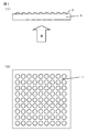
- FIG. 1 is a diagram schematically showing the light extraction structure 1.
- FIG. 2 is a diagram schematically illustrating the virtual structure 11 compared with the light extraction structure 1.
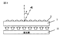
- FIG. 3 is a diagram for explaining I ( ⁇ °).
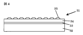
- FIG. 4 is a view showing a light extraction structure 31 having a laminated structure.
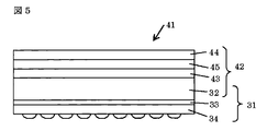
- FIG. 5 is a diagram schematically showing the light emitting device 41.
- FIG. 6 is a view showing a light emitting device 52 including the top emission type organic EL element 51 and the light extraction structure 1.
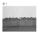
- FIG. 7 is a view showing a micrograph of a cross section of the UTE12.
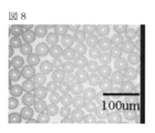
- FIG. 8 is a diagram showing a micrograph of the surface of UTE12.
- FIG. 9 is a diagram for explaining a method of measuring I ( ⁇ °).
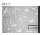
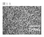
- FIG. 10 is a diagram showing a photomicrograph of the surface of UTE21.
- FIG. 11 is a view showing a micrograph of the surface of WF80.
- FIG. 1 is a diagram schematically showing a light extraction structure 1 according to an embodiment of the present invention.
- FIG. 1 (1) is a side view
- FIG. 1 (2) is a plan view.
- the light extraction structure 1 is a light extraction structure for an organic EL element provided on the extraction side of light emitted from the organic EL element.
- the light extraction structure 1 is provided on the outermost side in an organic EL element or a light emitting device on which this element is mounted. Since the light extraction structure 1 is provided on the light extraction side of the light emitted from the organic EL element, the light emitted from the organic EL element passes through the light extraction structure 1 and is emitted out of the light emitting device.
- the light emitting device may be further incorporated into another device or a housing.
- Organic EL elements are roughly classified into so-called bottom emission type elements and top emission type elements, depending on the direction of emitted light.
- the bottom emission type organic EL element emits light toward a support substrate on which the element is mounted. Therefore, the light extraction structure 1 may be provided as a support substrate, for example, in an organic EL element or a light emitting device in which this element is mounted.
- the top emission type organic EL element emits light to the side opposite to the support substrate. Therefore, in the light emitting device, the light extraction structure 1 may be provided as a sealing member that hermetically seals the organic EL element, for example.
- the light extraction structure 1 has an uneven structure on the surface 2 on the light extraction side.
- the surface 2 on the light extraction side corresponds to one surface of the pair of opposing surfaces of the light extraction structure 1 that is different from the surface on the organic EL element side (surface on the light incident side). Therefore, the surface 2 on the light extraction side forms an interface with the atmosphere in the light emitting device.
- the concavo-convex structure formed on the surface 2 on the light extraction side is a virtual structure in which the intensity of light incident on the light extraction structure 1 and emitted from the surface on the light extraction side is flat. When compared with the intensity of light emitted from the surface on the light extraction side, both the front intensity and the integrated intensity are 1.3 times or more.
- FIG. 2 schematically shows a virtual structure 11 compared with the light extraction structure 1 of the present invention.
- FIG. 2A is a side view and FIG. 2B is a plan view.
- the virtual structure 11 has a pair of opposing surfaces that are both planar. That is, the virtual structure 11 does not have an uneven structure.
- the virtual structure 11 has the same configuration as the light extraction structure 1 except that the shape of the surface is different.
- the front intensity of the light emitted from the light extraction structure 1 having the concavo-convex structure when the same light is incident on the light extraction structure 1 having the concavo-convex structure and the virtual structure 11 not having the concavo-convex structure is: It becomes 1.3 times or more of the front intensity of the light emitted from the virtual structure 11 having no uneven structure.
- the integrated intensity of the light emitted from the light extraction structure 1 having the concavo-convex structure when the same light is incident on the light extraction structure 1 having the concavo-convex structure and the virtual structure 11 having no concavo-convex structure is: It becomes 1.3 times or more of the integrated intensity of the light emitted from the virtual structure 11 having no uneven structure.
- the front intensity and the integrated intensity need only be 1.3 times or more, and there is no upper limit in particular, but it may not be appropriate if only the front intensity becomes too strong, and the magnification of the front intensity is, for example, 5 times or less.
- the strength magnification is, for example, 5 times or less.
- the front intensity of the emitted light represents the intensity of light in the thickness direction of the light extraction structure 1.
- the surface 2 on the light extraction side has a concavo-convex structure
- the normal direction of the plane and the thickness direction of the light extraction structure 1 when a plane obtained by macroscopically averaging the concavo-convex structure is assumed. Therefore, the front intensity of the emitted light represents the light intensity in the normal direction of the surface on the light extraction side of the light extraction structure 1.
- the integrated intensity of the emitted light is emitted not only in the normal direction but also in all directions with respect to the light emitted from the surface 2 on the light extraction side opposite to the side where the light source of the incident light is arranged. It is a value obtained by integrating the intensity of light to be transmitted.
- the organic EL element is used as a light source for various devices, but what is required as its characteristics varies depending on the mounted device. While there are devices that require high brightness in the normal direction as described in the background art, there are devices that require light that uniformly emits light in all directions. In other words, there is a device that is not suitable for a device that projects only in the normal direction and has high luminance. For example, a light extraction structure having high diffusibility is required for a light source that requires uniform light emission such as general illumination. Therefore, conventionally, even if the light intensity in a direction other than the normal direction (so-called oblique direction) is sacrificed, the research and development aiming to improve the front intensity and the uniform in all directions at the expense of the front intensity.
- the present inventors are useful as a light-emitting device if the light extraction structure 1 in which both the front intensity and the integrated intensity are 1.3 times or more is applied to the organic EL element. I found out.
- an organic EL element is used as a light source of an illuminating device, an illuminating device that has high front intensity of emitted light and can illuminate a room or the like is preferable, but both the front intensity and the integrated intensity are 1.3.
- an illumination device can be realized. This utilizes the property peculiar to the organic EL element that the element itself can be a planar light source (two-dimensional).
- inorganic LEDs, fluorescent lamps, and the like are point-like (zero-dimensional) or linear (one-dimensional) light sources, diffusivity is more important than frontal intensity when they are used as illumination devices. Therefore, application of a light extraction structure that has a high integrated intensity has been studied.
- the organic EL element can make the element itself a planar light source (two-dimensional)
- the light extraction structure 1 emits light from the surface on the light extraction side in a direction that forms an angle ⁇ ° with the normal direction when the light extraction structure is irradiated with light from a planar light source arranged in parallel.
- the intensity of light is I ( ⁇ °)
- the haze value is 60% or more
- the total light transmittance is 60% or more.
- the ratio of I ( ⁇ °) may be referred to as a diffusion parameter.
- the haze value is represented by the following formula.
- the haze value can be measured by the method described in JIS K 7136 “Plastic—How to Obtain Haze of Transparent Material”.
- Haze value (cloudiness value) (diffuse transmittance (%) / total light transmittance (%)) ⁇ 100 (%).
- the total light transmittance can be measured by the method described in JIS K 7361-1 “Testing method of total light transmittance of plastic-transparent material”.
- FIG. 3 is a diagram for explaining I ( ⁇ °). The intensity of light emitted in the normal direction is defined as I (0).
- the planar light source 21 is disposed in parallel with the light extraction structure 1 so that the surface 2 on the light extraction side and the light emitting surface are parallel to each other. As described above, since the organic EL element itself becomes a planar light source, the planar light source 21 simulates the organic EL element.
- a method for measuring I ( ⁇ ) will be described in the section of Examples.
- I (35) represents the light intensity in a direction inclined by 35 ° from the normal direction
- I (70) represents the light intensity in a direction inclined by 70 ° from the normal direction.
- I (35) / I (70) is higher, light is emitted in the front direction. Therefore, when it is higher than 5, the light extraction structure 1 can be suitably used for, for example, a lighting device.
- the light extraction structure 1 preferably further satisfies the following formula (2).
- the light extraction structure 1 is preferably used for, for example, a lighting device. it can. If I (0) / I (35) is too high, only the light intensity in the front direction becomes too high, so 10 or less is preferable for illuminating a wide range.
- the concavo-convex structure on the surface 2 on the light extraction side of the light extraction structure 1 is preferably configured by a plurality of granular structures dispersed and arranged on the surface.
- the granular structure may be integrally formed on the surface portion on the light extraction side, or may be attached on the surface.
- the granular structures may be arranged periodically or aperiodically. When the granular structures are arranged aperiodically, light interference caused by the granular structures can be suppressed, so that the occurrence of moire or the like can be prevented. Examples of the light extraction structure in which a plurality of granular structures are dispersed on the surface are shown in FIGS.
- the size (that is, the width) of the convex or concave shape in the direction parallel to the surface of the light extraction structure 1 is too large, the luminance on the surface of the light extraction structure 1 tends to be uneven and is too small. Therefore, the production cost of the light extraction structure 1 tends to increase, so that the thickness is preferably 0.5 ⁇ m to 100 ⁇ m, more preferably 1 ⁇ m to 50 ⁇ m.
- the height in the normal direction of the surface of the light extraction structure 1 for each convex or concave shape is usually determined by the width of each convex or concave shape and the period in which the concavo-convex structure is provided.
- each shape or not more than the period in which the concavo-convex structure is formed is preferably 0.25 ⁇ m to 70 ⁇ m, and preferably 0.5 ⁇ m to 50 ⁇ m.
- the shape of the convex surface or the concave surface is not particularly limited, but preferably has a curved surface, for example, a hemispherical shape. It is preferable that the concave surface or the convex surface be arranged aperiodically so that moire can be prevented in the same manner as described above.
- the area of the region where the concave and convex surfaces are formed in the surface 2 on the light extraction side of the light extraction structure 1 is the light extraction structure 60% or more of the surface area of the body 1 is preferable, and the upper limit is a value in a state where the concave surface and the convex surface are laid on the surface.
- the material which comprises the light extraction structure 1 should just be a transparent material, and may use inorganic substances, such as glass, and organic substance (a low molecular compound or a high molecular compound).
- Examples of the polymer compound used for the light extraction structure 1 include polyarylate, polycarbonate, polycycloolefin, polyethylene naphthalate, polyethylene sulfonic acid, and polyethylene terephthalate.
- the thickness of the light extraction structure 1 is not particularly limited, but if it is too thin, handling becomes difficult, and if it is too thick, the total light transmittance tends to be low, so 50 ⁇ m to 2 mm is preferable, and 80 ⁇ m to 1. 5 mm.
- a light extraction structure made of an inorganic material such as glass can be obtained by etching a flat base made of an inorganic material.
- a concavo-convex structure can be formed by patterning a protective film on the surface of a base made of an inorganic material and performing liquid phase etching or gas phase etching.
- the protective film can be patterned using, for example, a photoresist.
- a concavo-convex structure can be formed on the surface by the following methods (1) to (5), for example. (1) A method of transferring the concavo-convex shape of the metal plate by pressing the concavo-convex metal plate against a heated film.
- a method of rolling a polymer sheet or film using a roll having an uneven surface (2) A method of rolling a polymer sheet or film using a roll having an uneven surface. (3) A method of forming a film by dropping a solution or dispersion containing an organic material onto a base having an uneven surface. (4) A method in which after forming a film made of a polymerizable monomer, a part of the film is selectively photopolymerized to remove an unpolymerized part. (5) A method in which a polymer solution is cast on a base under high humidity conditions, and a water droplet structure is transferred to the surface.
- the light extraction structure may have a single layer structure or a stacked structure.
- FIG. 4 shows a light extraction structure 31 having a laminated structure.
- the light extraction structure 31 having a laminated structure is configured by laminating a support substrate 32, an adhesive layer 33, and a film 34 having a surface 35 on the light extraction side in this order. As shown in FIG. 4, the film 34 is bonded to the support substrate 32 with the surface opposite to the light extraction side surface 35 having an uneven structure facing the support substrate 32.
- a thermosetting resin, a photocurable resin, an adhesive, an adhesive, or the like can be used.
- the film 34 can be bonded to the support substrate 32 by heating the thermosetting resin at a predetermined temperature.
- the film 34 can be adhered to the support substrate 32 by, for example, irradiating the photocurable resin with ultraviolet rays.
- the adhesive layer need not be used, and the adhesive layer needs to be used also when the uneven structure is formed by processing the surface of the support substrate 32. Absent.
- the shape of the surface of the film 34 on the light extraction side is the same as that of the surface of the light extraction structure 1 described above on the light extraction side.
- the absolute value of the difference between the maximum value and the minimum value among the refractive index nf of the film 34, the refractive index na of the adhesive layer 33, and the refractive index ns of the support substrate 32 is preferably less than 0.2. That is, it is preferable that the light extraction structure 31 satisfies the following expression (3).
- the film 34 and the support substrate 32 constituting the light extraction structure 31 having a laminated structure may be made of a transparent material, like the light extraction structure 1 described above.
- the light extraction structure 1 is exemplified as a material of the light extraction structure 1. Can be used.
- the thickness of the film 34 and the support substrate 32 is not particularly limited, but the thickness of the light extraction structure 31 having a laminated structure in which the film 34 and the support substrate 32 are bonded with the adhesive layer 33 interposed is preferably 50 ⁇ m to 2 mm. More preferably, it is 80 ⁇ m to 1.5 mm.
- the light-emitting device includes an organic EL element including the organic electroluminescence element using the above-described light extraction structure provided on the extraction side of light emitted from the organic electroluminescence element.
- the organic EL element usually includes a support substrate.
- FIG. 5 is a diagram schematically showing the light emitting device 41 of the present embodiment.
- FIG. 5 shows a light emitting device 41 including an organic EL element 42 using a light extraction structure 31 constituting a laminated structure, as an example of implementation.
- the organic EL element 42 is a bottom emission type element that emits light toward the support substrate.
- the light extraction structure 31 is not limited to a laminated structure, and may have a single layer structure.
- a support substrate having a concavo-convex structure on the surface may be used as the light extraction structure.
- the light extraction structure 31 functions as a light extraction structure and also functions as a support substrate on which the organic EL element 42 is mounted.
- FIG. 5 shows the light emitting device 41 in which the electrode of the organic EL element 42 is disposed in contact with the support substrate 32, a predetermined member may be interposed between the electrode and the support substrate 32.
- the light extraction structure 31 is arranged so that the surface 35 on the light extraction side is positioned on the outermost surface of the light emitting device 41.
- the light emitting device 41 in which the organic EL element 42 is mounted on the light extraction structure 31 improves the front intensity and the integrated intensity of the emitted light. Therefore, the light emitting device 41 can be used as a light source suitable for an illumination device, for example.
- the organic EL element includes a pair of electrodes 43 and 44 and a light emitting layer 45 disposed between the electrodes.
- One of the pair of electrodes 43 and 44 functions as an anode, and the other electrode functions as a cathode.
- the pair of electrodes 43 and 44 in consideration of the simplicity and characteristics of the process, not only a single light emitting layer but also a plurality of light emitting layers or predetermined layers may be provided.
- the bottom emission type organic EL element is provided in the light extraction structure 31, one of the electrodes 43, 44 disposed near the light extraction structure 31 has light transmittance. It is comprised by the electrode shown. That is, the light emitted from the light emitting layer is emitted to the outside through the one electrode 43 exhibiting optical transparency and the light extraction structure 31. Since the light extraction structure of the present invention can be suitably used for a planar light source, the size of the organic EL element to which the light extraction structure is applied is more than the extent that the characteristics as a planar light source appear. For example, 10 mm square or more is preferable in plan view. Details of the configuration of the organic EL element will be described later.
- the light extraction structure of the present invention can also be used for a so-called top emission type organic EL element that emits light to the side opposite to the support substrate on which the organic EL element is mounted.
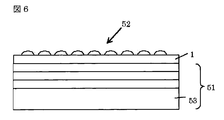
- FIG. 6 shows a light emitting device 52 including a top emission type organic EL element 51 and the light extraction structure 1.
- the light extraction structure 1 is not limited to a single layer structure, and may have a laminated structure.
- the light emitting device 52 of the present embodiment includes a support substrate 53 on which the organic EL element 51 is mounted. Since the organic EL element 51 emits light to the side opposite to the support substrate 53, the light extraction structure 1 provided on the light extraction side of the light emitted from the organic EL element is supported on the basis of the organic EL element 51.
- the organic EL element 51 is sandwiched between the light extraction structure 1 and the support substrate 53.
- a predetermined member may be interposed between the light extraction structure 1 and the organic EL element 51. Since the organic EL element emits light to the side opposite to the support substrate 53 (light extraction structure 1 side), the electrode disposed near the light extraction structure 1 of the pair of electrodes exhibits light transmittance. Consists of electrodes. That is, light emitted from the light emitting layer is emitted to the outside through the light transmissive electrode and the light extraction structure 1.
- Such a light extraction structure 1 also functions as a sealing member, for example. (Organic EL device)
- the configuration of the organic EL element will be described in more detail.
- a predetermined layer may be provided between the pair of electrodes, and the light emitting layer is not limited to one layer, and a plurality of layers may be provided.
- the layer provided between the cathode and the light emitting layer include an electron injection layer, an electron transport layer, and a hole blocking layer.
- the layer in contact with the cathode is referred to as an electron injection layer, and the layer excluding this electron injection layer is referred to as an electron transport layer.
- the electron injection layer has a function of improving electron injection efficiency from the cathode.
- the electron transport layer has a function of improving electron injection from the layer in contact with the surface on the cathode side.
- the hole blocking layer has a function of blocking hole transport.
- these layers may also serve as the hole blocking layer.
- the fact that the hole blocking layer has a function of blocking hole transport makes it possible, for example, to produce an element that allows only a hole current to flow, and confirm the blocking effect by reducing the current value.
- Examples of the layer provided between the anode and the light emitting layer include a hole injection layer, a hole transport layer, and an electron block layer.
- the layer in contact with the anode is called a hole injection layer, and the layers other than the hole injection layer are positive. It is called a hole transport layer.
- the hole injection layer has a function of improving hole injection efficiency from the anode.
- the hole transport layer has a function of improving hole injection from a layer in contact with the surface on the anode side.
- the electron blocking layer has a function of blocking electron transport. When the hole injection layer and / or the hole transport layer have a function of blocking electron transport, these layers may also serve as the electron block layer.
- the electron blocking layer has a function of blocking electron transport makes it possible, for example, to produce an element that allows only electron current to flow and confirm the blocking effect by reducing the current value.
- the electron injection layer and the hole injection layer may be collectively referred to as a charge injection layer, and the electron transport layer and the hole transport layer may be collectively referred to as a charge transport layer.
- An example of a layer structure that can be taken by the organic EL element of the present embodiment is shown below.
- anode / light emitting layer / cathode b) anode / hole injection layer / light emitting layer / cathode c) anode / hole injection layer / light emitting layer / electron injection layer / cathode d) anode / hole injection layer / light emitting layer / Electron transport layer / cathode e) anode / hole injection layer / light emitting layer / electron transport layer / electron injection layer / cathode f) anode / hole transport layer / light emitting layer / cathode g) anode / hole transport layer / light emitting layer / Electron injection layer / cathode h) anode / hole transport layer / light emitting layer / electron transport layer / cathode i) anode / hole transport layer / light emitting layer / electron transport layer / electron injection layer / cathode j) anode / hole Injection
- the organic EL element of the present embodiment may have two or more light emitting layers.
- the configuration of the organic EL element having two light emitting layers is as follows. And the layer structure shown in the following q).
- the two (structural unit A) layer structures may be the same or different.
- the charge generation layer is a layer that generates holes and electrons by applying an electric field.
- the charge generation layer include a thin film made of vanadium oxide, indium tin oxide (abbreviated as ITO), molybdenum oxide, or the like.
- ITO indium tin oxide
- the order of the layers to be laminated, the number of layers, and the thickness of each layer can be appropriately set in consideration of the light emission efficiency and the element lifetime.
- the material and forming method of each layer constituting the organic EL element will be described more specifically.
- a substrate that does not change in the process of manufacturing the organic EL element is suitably used. For example, glass, plastic, a polymer film, a silicon plate, and a laminate of these are used.
- a commercially available substrate can be used as the substrate, and it can be produced by a known method.
- an electrode exhibiting optical transparency is used for the anode.
- the electrode exhibiting light transmittance a thin film of metal oxide, metal sulfide, metal or the like can be used, and an electrode having high electrical conductivity and light transmittance is preferably used.
- thin films made of indium oxide, zinc oxide, tin oxide, ITO, indium zinc oxide (abbreviated as IZO), gold, platinum, silver, copper, and the like are used.
- ITO, IZO Or a thin film made of tin oxide is preferably used.
- a method for producing the anode include a vacuum deposition method, a sputtering method, an ion plating method, and a plating method.
- an organic transparent conductive film such as polyaniline or a derivative thereof, polythiophene or a derivative thereof may be used.
- the film thickness of the anode is appropriately set in consideration of required characteristics and process simplicity, and is, for example, 10 nm to 10 ⁇ m, preferably 20 nm to 1 ⁇ m, and more preferably 50 nm to 500 nm.
- ⁇ Hole injection layer> As the hole injection material constituting the hole injection layer, oxides such as vanadium oxide, molybdenum oxide, ruthenium oxide, and aluminum oxide, phenylamine type, starburst type amine type, phthalocyanine type, amorphous carbon, polyaniline, And polythiophene derivatives.
- oxides such as vanadium oxide, molybdenum oxide, ruthenium oxide, and aluminum oxide, phenylamine type, starburst type amine type, phthalocyanine type, amorphous carbon, polyaniline, And polythiophene derivatives.
- the method for forming the hole injection layer include film formation from a solution containing a hole injection material.
- a hole injection layer can be formed by coating a film containing a hole injection material by a predetermined coating method and solidifying the solution.
- the solvent used for film formation from a solution is not particularly limited as long as it dissolves the hole injection material.
- Chlorine solvents such as chloroform, methylene chloride, dichloroethane, ether solvents such as tetrahydrofuran, toluene, xylene And aromatic hydrocarbon solvents such as acetone, ketone solvents such as acetone and methyl ethyl ketone, ester solvents such as ethyl acetate, butyl acetate and ethyl cellosolve acetate, and water.
- coating methods spin coating method, casting method, micro gravure coating method, gravure coating method, bar coating method, roll coating method, wire bar coating method, dip coating method, spray coating method, screen printing method, flexographic printing method, offset A printing method, an inkjet printing method, etc. can be mentioned.
- the film thickness of the hole injection layer is appropriately set in consideration of required characteristics and process simplicity, and is, for example, 1 nm to 1 ⁇ m, preferably 2 nm to 500 nm, and more preferably 5 nm to 200 nm.
- ⁇ Hole transport layer As the hole transport material constituting the hole transport layer, polyvinylcarbazole or a derivative thereof, polysilane or a derivative thereof, a polysiloxane derivative having an aromatic amine in a side chain or a main chain, a pyrazoline derivative, an arylamine derivative, a stilbene derivative, Triphenyldiamine derivative, polyaniline or derivative thereof, polythiophene or derivative thereof, polyarylamine or derivative thereof, polypyrrole or derivative thereof, poly (p-phenylene vinylene) or derivative thereof, or poly (2,5-thienylene vinylene) or Examples thereof include derivatives thereof.
- hole transport materials include polyvinyl carbazole or derivatives thereof, polysilane or derivatives thereof, polysiloxane derivatives having aromatic amine compound groups in the side chain or main chain, polyaniline or derivatives thereof, polythiophene or derivatives thereof, poly Polymeric hole transport materials such as arylamine or derivatives thereof, poly (p-phenylene vinylene) or derivatives thereof, or poly (2,5-thienylene vinylene) or derivatives thereof are preferred, and polyvinylcarbazole or derivatives thereof are more preferred. , Polysilane or a derivative thereof, and a polysiloxane derivative having an aromatic amine in the side chain or main chain.
- a low-molecular hole transport material it is preferably used by being dispersed in a polymer binder.
- the method for forming the hole transport layer is not particularly limited, but in the case of a low molecular hole transport material, film formation from a mixed solution containing a polymer binder and a hole transport material can be exemplified.
- molecular hole transport materials include film formation from a solution containing a hole transport material.
- the solvent used for film formation from a solution is not particularly limited as long as it can dissolve a hole transport material.
- Chlorine solvents such as chloroform, methylene chloride, dichloroethane, ether solvents such as tetrahydrofuran, toluene, xylene And aromatic hydrocarbon solvents such as acetone, ketone solvents such as acetone and methyl ethyl ketone, and ester solvents such as ethyl acetate, butyl acetate, and ethyl cellosolve acetate.
- the film forming method from a solution include the same coating method as the above-described film forming method of the hole injection layer.
- the polymer binder to be mixed those that do not extremely inhibit charge transport are preferable, and those that weakly absorb visible light are preferably used.
- the film thickness of the hole transport layer the optimum value varies depending on the material to be used, the drive voltage and the light emission efficiency are appropriately set so as to have an appropriate value, and at least a thickness that does not cause pinholes is required. If the thickness is too thick, the drive voltage of the element becomes high, which is not preferable. Therefore, the thickness of the hole transport layer is, for example, 1 nm to 1 ⁇ m, preferably 2 nm to 500 nm, and more preferably 5 nm to 200 nm.
- the light emitting layer is usually formed of an organic substance that mainly emits fluorescence and / or phosphorescence, or an organic substance and a dopant that assists the organic substance.
- the dopant is added, for example, in order to improve the luminous efficiency and change the emission wavelength.
- the organic substance contained in the light emitting layer may be a low molecular compound or a high molecular compound.
- a polymer compound having higher solubility in a solvent than a low molecule is preferably used in the coating method, and therefore the light-emitting layer preferably contains a polymer compound, and the polymer compound has a polystyrene-equivalent number average molecular weight.
- the light emitting material constituting the light emitting layer includes the following dye materials, metal complex materials, polymer materials, and dopant materials.
- Dye material examples include cyclopentamine derivatives, tetraphenylbutadiene derivative compounds, triphenylamine derivatives, oxadiazole derivatives, pyrazoloquinoline derivatives, distyrylbenzene derivatives, distyrylarylene derivatives, pyrrole derivatives, thiophene ring compounds.
- metal complex materials include rare earth metals such as Tb, Eu, and Dy, or Al, Zn, Be, Ir, Pt, etc. as a central metal, and oxadiazole, thiadiazole, phenylpyridine, phenylbenzimidazole, quinoline.
- Examples include metal complexes having a structure or the like as a ligand, such as iridium complexes, platinum complexes, etc., metal complexes having light emission from a triplet excited state, aluminum quinolinol complexes, benzoquinolinol beryllium complexes, benzoxazolyl zinc A complex, a benzothiazole zinc complex, an azomethylzinc complex, a porphyrin zinc complex, a phenanthroline europium complex, and the like can be given.
- metal complexes having a structure or the like as a ligand such as iridium complexes, platinum complexes, etc., metal complexes having light emission from a triplet excited state, aluminum quinolinol complexes, benzoquinolinol beryllium complexes, benzoxazolyl zinc A complex, a benzothiazole zinc complex, an azomethylzinc complex, a porphyrin zinc complex, a phenanthro
- Polymer material As polymer materials, polyparaphenylene vinylene derivatives, polythiophene derivatives, polyparaphenylene derivatives, polysilane derivatives, polyacetylene derivatives, polyfluorene derivatives, polyvinylcarbazole derivatives, the above dye materials and metal complex light emitting materials are polymerized. The thing etc. can be mentioned.
- the material that emits blue light examples include distyrylarylene derivatives, oxadiazole derivatives, and polymers thereof, polyvinylcarbazole derivatives, polyparaphenylene derivatives, and polyfluorene derivatives.
- polymer materials such as polyvinylcarbazole derivatives, polyparaphenylene derivatives, and polyfluorene derivatives are preferred.
- materials that emit green light include quinacridone derivatives, coumarin derivatives, and polymers thereof, polyparaphenylene vinylene derivatives, polyfluorene derivatives, and the like.
- polymer materials such as polyparaphenylene vinylene derivatives and polyfluorene derivatives are preferred.
- the material that emits red light include a coumarin derivative, a thiophene ring compound, a polymer thereof, a polyparaphenylene vinylene derivative, a polythiophene derivative, and a polyfluorene derivative.
- polymer materials such as polyparaphenylene vinylene derivatives, polythiophene derivatives, and polyfluorene derivatives are preferable.
- a material that emits white light a mixture of materials that emit light in the above-described blue, green, and red colors, or a component that becomes a material that emits light in each color as a monomer, and a polymer obtained by polymerizing this as a material are used. Also good.
- a light emitting layer formed using materials that emit light of each color may be stacked to realize an element that emits white light as a whole.
- Dopant material examples include perylene derivatives, coumarin derivatives, rubrene derivatives, quinacridone derivatives, squalium derivatives, porphyrin derivatives, styryl dyes, tetracene derivatives, pyrazolone derivatives, decacyclene, phenoxazone, and the like.
- the thickness of such a light emitting layer is usually about 2 nm to 200 nm.
- Examples of the solvent used for film formation from a solution include the same solvents as those used for forming a hole injection layer from the aforementioned solution.
- a method for applying a solution containing a light emitting material a spin coating method, a casting method, a micro gravure coating method, a gravure coating method, a bar coating method, a roll coating method, a wire bar coating method, a dip coating method, a slit coating method, a capillary
- Examples of the coating method include coating methods such as a coating method, a spray coating method, and a nozzle coating method, and a gravure printing method, a screen printing method, a flexographic printing method, an offset printing method, a reverse printing method, and an inkjet printing method.
- a printing method such as a gravure printing method, a screen printing method, a flexographic printing method, an offset printing method, a reverse printing method, and an ink jet printing method is preferable in that pattern formation and multicolor coating are easy.
- a vacuum deposition method can be used.
- a method of forming a light emitting layer only at a desired place by laser transfer or thermal transfer can be used.
- Electrode transport material constituting the electron transport layer
- known materials can be used, such as oxadiazole derivatives, anthraquinodimethane or derivatives thereof, benzoquinone or derivatives thereof, naphthoquinone or derivatives thereof, anthraquinones or derivatives thereof, tetracyanoanthra Quinodimethane or derivatives thereof, fluorenone derivatives, diphenyldicyanoethylene or derivatives thereof, diphenoquinone derivatives, or metal complexes of 8-hydroxyquinoline or derivatives thereof, polyquinoline or derivatives thereof, polyquinoxaline or derivatives thereof, polyfluorene or derivatives thereof, etc. Can be mentioned.
- an oxadiazole derivative benzoquinone or a derivative thereof, anthraquinone or a derivative thereof, a metal complex of 8-hydroxyquinoline or a derivative thereof, a polyquinoline or a derivative thereof, a polyquinoxaline or a derivative thereof, a polyfluorene Or a derivative thereof is preferable, and 2- (4-biphenylyl) -5- (4-t-butylphenyl) -1,3,4-oxadiazole, benzoquinone, anthraquinone, tris (8-quinolinol) aluminum, and polyquinoline are further included. preferable.
- the method for forming the electron transport layer there are no particular restrictions on the method for forming the electron transport layer, but for low molecular weight electron transport materials, vacuum deposition from powder or film formation from a solution or a molten state can be used.
- the material include film formation from a solution or a molten state.
- a polymer binder may be used in combination.
- the method for forming an electron transport layer from a solution include the same film formation method as the method for forming a hole injection layer from a solution described above.
- the film thickness of the electron transport layer varies depending on the material used, and is set appropriately so that the drive voltage and the light emission efficiency are appropriate, and at least a thickness that does not cause pinholes is required, and is too thick.
- the thickness of the electron transport layer is, for example, 1 nm to 1 ⁇ m, preferably 2 nm to 500 nm, and more preferably 5 nm to 200 nm.
- an optimal material is appropriately selected according to the type of the light emitting layer, and an alloy containing one or more of alkali metals, alkaline earth metals, alkali metals and alkaline earth metals, Alkali metal or alkaline earth metal oxides, halides, carbonates, mixtures of these substances, and the like can be given.
- alkali metals, alkali metal oxides, halides, and carbonates include lithium, sodium, potassium, rubidium, cesium, lithium oxide, lithium fluoride, sodium oxide, sodium fluoride, potassium oxide, potassium fluoride , Rubidium oxide, rubidium fluoride, cesium oxide, cesium fluoride, lithium carbonate, and the like.
- alkaline earth metal, alkaline earth metal oxides, halides and carbonates include magnesium, calcium, barium, strontium, magnesium oxide, magnesium fluoride, calcium oxide, calcium fluoride, barium oxide, fluoride Examples thereof include barium, strontium oxide, strontium fluoride, and magnesium carbonate.
- the electron injection layer may be composed of a laminate in which two or more layers are laminated, and examples thereof include LiF / Ca.
- the electron injection layer is formed by vapor deposition, sputtering, printing, or the like.
- the thickness of the electron injection layer is preferably about 1 nm to 1 ⁇ m.
- a material for the cathode is preferably a material having a low work function, easy electron injection into the light emitting layer, and high electrical conductivity.
- a material having a high visible light reflectivity is preferable as the cathode material in order to reflect light emitted from the light emitting layer to the anode side by the cathode.
- an alkali metal, an alkaline earth metal, a transition metal, a Group 13 metal of the periodic table, or the like can be used.
- the cathode material include lithium, sodium, potassium, rubidium, cesium, beryllium, magnesium, calcium, strontium, barium, aluminum, scandium, vanadium, zinc, yttrium, indium, cerium, samarium, europium, terbium, ytterbium, and the like.
- An alloy, graphite, or a graphite intercalation compound is used.
- alloys include magnesium-silver alloys, magnesium-indium alloys, magnesium-aluminum alloys, indium-silver alloys, lithium-aluminum alloys, lithium-magnesium alloys, lithium-indium alloys, calcium-aluminum alloys, and the like. it can.
- a transparent conductive electrode made of a conductive metal oxide and a conductive organic material can be used.
- examples of the conductive metal oxide include indium oxide, zinc oxide, tin oxide, ITO, and IZO
- examples of the conductive organic substance include polyaniline or a derivative thereof, polythiophene or a derivative thereof, and the like.
- the cathode may be composed of a laminate in which two or more layers are laminated. In some cases, the electron injection layer is used as a cathode.
- the film thickness of the cathode is appropriately designed in consideration of required characteristics and process simplicity, and is, for example, 10 nm to 10 ⁇ m, preferably 20 nm to 1 ⁇ m, and more preferably 50 nm to 500 nm.
- Examples of the method for producing the cathode include a vacuum deposition method, a sputtering method, and a laminating method in which a metal thin film is thermocompression bonded.
- Examples of the material for the insulating layer include metal fluorides, metal oxides, and organic insulating materials.
- an organic EL element provided with an insulating layer having a thickness of 2 nm or less an organic EL element having an insulating layer having a thickness of 2 nm or less adjacent to the cathode and an insulating layer having a thickness of 2 nm or less adjacent to the anode are provided. Can be mentioned.
- the light extraction structure is disposed on the surface portion of the organic EL element in the light extraction direction.
- the surface opposite to the organic EL element side has an uneven structure, at least a part of the surface of the light emitting device is formed in an uneven shape.
- Part of the light emitted from the organic EL element enters the light extraction structure, is refracted and diffused on the uneven surface, and is emitted to the outside of the light emitting device.
- the light extraction structure provided in the light-emitting device has a concavo-convex structure in which both the front intensity and the integrated intensity are 1.3 times that of a virtual structure with a flat surface. Instead, the overall brightness is improved. Since the organic EL element can be formed in a planar shape, a light-emitting device including such a light extraction structure as described above can be suitably used as a lighting device.
- each example and comparative example a current of 0.15 mA was passed through the organic EL element, and the emission intensity in the normal direction (front direction) at that time and the integration intensity using an integrating sphere were measured.
- a light-emitting device in which an organic EL element was produced on a glass substrate having a flat surface was used as a reference light-emitting device, and the characteristics of the reference light-emitting device and the light-emitting devices of the examples and comparative examples were compared.
- a glass substrate having a flat surface corresponds to a virtual structure having a flat surface on the light extraction side.
- Example 1 A substrate on which an anode made of an ITO thin film having a predetermined pattern shape was formed was prepared, and this substrate was subjected to UV / O 3 cleaning for 20 minutes.
- a two-stage filtration was performed on a suspension of poly (3,4) ethylenedioxythiophene / polystyrene sulfonic acid (trade name: BaytronP CH8000, manufactured by Starck Vitec Co., Ltd.).
- poly (3,4) ethylenedioxythiophene / polystyrene sulfonic acid (trade name: BaytronP CH8000, manufactured by Starck Vitec Co., Ltd.).
- a 0.45 ⁇ m diameter filter was used
- a 0.2 ⁇ m diameter filter was used.
- the filtered solution was applied on the anode by a spin coating method, and further heat-treated at 200 ° C. for 15 minutes on a hot plate in an air atmosphere to form a hole injection layer having a thickness of 65 nm.
- a xylene solution having a concentration of Lumation WP1330 manufactured by SUMION
- This solution was applied on the hole injection layer by a spin coating method, and further heat-treated at 130 ° C. for 60 minutes on a hot plate in a nitrogen atmosphere to form a light emitting layer having a thickness of 65 nm.
- the substrate on which the light emitting layer was formed was introduced into a vacuum vapor deposition machine, and Ba and Al were sequentially deposited at a thickness of 5 nm and 80 nm, respectively, to form a cathode.
- the metal deposition was started after the degree of vacuum reached 1 ⁇ 10 ⁇ 4 Pa or less.
- a photocurable sealant is applied to the periphery of the sealing glass with a dispenser, and the substrate on which the organic EL element is formed and the sealing glass are bonded together in a nitrogen atmosphere.
- a film UTE12 (refractive index 1.5, thickness 188 ⁇ m) made by MNtech having a concavo-convex structure in which a plurality of granular structures are dispersed and arranged on the surface, and a non-carrier adhesive (refractive index 1.. It was bonded to a glass substrate using 5). At that time, the film was bonded so that the concavo-convex structure was disposed on the outermost surface.
- Example 1 the glass substrate corresponds to the support substrate, the MNtech film UTE12 corresponds to the film, the non-carrier adhesive corresponds to the adhesive layer, the glass substrate, the non-carrier adhesive, and the MNtech film UTE12.
- FIG. 7 shows a micrograph of the cross section of UTE12
- FIG. 8 shows a micrograph of the surface.
- the UTE 12 has a plurality of granular uneven structures.
- the total light transmittance of UTE12 is 68.4%
- haze is 82.6%
- the diffusion parameter I (35) / I (70) is 7.2
- I (0) / I (35) is 1.7. Met.
- a halogen lamp SPH-100N manufactured by Chuo Seiki Co., Ltd. was used as the light source.
- a planar light source When a planar light source is used as the light source, light with a specific incident angle is not incident on the light extraction structure, but light with ⁇ 90 ° ⁇ ° ⁇ 90 ° is incident simultaneously.
- the incident angle ⁇ ° of the incident light is changed by 5 ° in a range of ⁇ 80 ° ⁇ ⁇ ° ⁇ 80 °, and the intensity of the emitted light in the ⁇ ° direction measured at each incident angle.
- Example 2 In the same manner as in Example 1, an organic EL element is formed on a glass substrate, and a film UTE21 (refractive index 1.. 5 and a thickness of 188 ⁇ m) were bonded to a glass substrate using a non-carrier adhesive (refractive index 1.5). In that case, the film was bonded so that the uneven structure of the film was disposed on the outermost surface.
- FIG. 10 shows a photomicrograph of the surface of UTE21. As shown in FIG. 10, the UTE 21 has a plurality of granular uneven structures. The total light transmittance of UTE21 is 63.4%, haze is 78.7%, diffusion parameter I (35) / I (70) is 8.4, and I (0) / I (35) is 2.0.
- Example 3 When the light emitting device of this example was compared with a standard light emitting device in which UTE21 was not bonded to the glass substrate, the front luminance was 1.45 times and the integrated intensity was 1.34 times.
- Example 3 In the same manner as in Example 1, an organic EL element is formed on a glass substrate, and a wave front film WF80 (refractive index: 1.) having a concavo-convex structure constituted by a plurality of granular structures dispersed and arranged on the surface. 5, a thickness of 80 ⁇ m) was bonded to the substrate using a non-carrier adhesive (refractive index 1.5). In that case, the film was bonded so that the uneven structure of the film was disposed on the outermost surface.
- FIG. 11 shows a micrograph of the surface of WF80.
- the WF 80 has a plurality of granular uneven structures.
- WF80 has a total light transmittance of 75.1%, a haze of 89.3%, a diffusion parameter I (35) / I (70) of 6.5, and I (0) / I (35) of 1.1. Met.
- the front luminance was 1.42 times and the integrated intensity was 1.31 times.
- Example 1 Comparative Example 1
- a 3M company film BEF100 reffractive index 1.5, thickness 150 ⁇ m
- a non-carrier adhesive reffractive index 1.5
- the film was bonded so that the uneven structure of the film was disposed on the outermost surface.
- Comparative Example 2 Film Opulse PCM1 (Ewa Shoko Co., Ltd.) having an uneven structure formed by forming an organic EL element on a glass substrate in the same manner as in Example 1 and arranging a plurality of granular structures dispersed on the surface.
- a refractive index of 1.5 and a thickness of 120 ⁇ m was bonded to a glass substrate using a non-carrier pressure-sensitive adhesive (refractive index of 1.5). In that case, the film was bonded so that the uneven structure of the film was disposed on the outermost surface.
- PCM1 has a total light transmittance of 92.7%, a haze of 86.0%, a diffusion parameter I (35) / I (70) of 2.0, and I (0) / I (35) of 1. .3.
- the front luminance was 1.24 times and the integrated intensity was 1.26 times.
- Examples 1, 2, and 3 have higher light extraction efficiency than Comparative Examples 1 and 2, and both front luminance and integrated intensity are 1.3 times or more than the standard light emitting device. It was.
- a light extraction structure that realizes an organic EL element that can be used in a device that requires other characteristics in addition to luminance in the normal direction, a light-emitting device that uses this light extraction structure, and illumination An apparatus can be provided.
Abstract
Description
有機EL素子内部で発生した光は電極を通って外に出射し、この光が表示装置や照明装置の光源として利用される。しかしながら素子内部で発生した光の全てが外に出射するわけではなく、その大部分は、反射などによって素子内部に閉じ込められ、有効に利用されていない。
光源としては所定の輝度が求められるため、反射などを抑制する構造を備えるプリズムシートを有機EL素子の光取り出し側に配置することで、法線方向に出射される光の割合を高くし、法線方向の輝度を高めた発光装置が提案されている(例えば、特開2007−5277号公報参照)。 The organic EL element is a light emitting element using an organic material as a light emitting material, and includes a pair of electrodes (anode and cathode) and a light emitting layer provided between the electrodes. When a voltage is applied to the organic EL element, holes are injected from the anode and electrons are injected from the cathode, and the holes and electrons combine in the light emitting layer to emit light.
Light generated inside the organic EL element is emitted to the outside through the electrode, and this light is used as a light source for a display device or a lighting device. However, not all of the light generated inside the element is emitted outside, and most of the light is confined inside the element by reflection or the like and is not effectively used.
Since a predetermined luminance is required as a light source, a prism sheet having a structure for suppressing reflection and the like is arranged on the light extraction side of the organic EL element, thereby increasing the ratio of light emitted in the normal direction. A light-emitting device with increased brightness in the line direction has been proposed (see, for example, Japanese Patent Application Laid-Open No. 2007-5277).
本発明の目的は、法線方向の輝度に加えて他の特性も求められる装置に利用可能な有機EL素子を実現する光取り出し構造体、およびこの光取り出し構造体を用いた発光装置、並びに照明装置を提供することである。
本発明は、下記光取り出し構造体、発光装置及び照明装置に関する。
〔1〕有機エレクトロルミネッセンス素子が放射する光の取り出し側に設けられる有機エレクトロルミネッセンス素子用の光取り出し構造体であって、
該構造体に入射し、光取り出し側の表面から出射する光の強度を、光取り出し側の表面が平面状の仮想構造体の光の取り出し側の表面から出射する光の強度と比較したときに、正面強度および積分強度のいずれもが1.3倍以上となる凹凸構造を、光取り出し側の表面に有する光取り出し構造体。
〔1〕の構造体は、より具体的には、
有機エレクトロルミネッセンス素子が放射する光の取り出し側に設けられる有機エレクトロルミネッセンス素子用の光取り出し構造体であって、
該構造体は、該構造体の光取り出し側の表面に凹凸構造を有し、
該凹凸構造は、
有機エレクトロルミネッセンス素子が放射する光が該構造体の光入射側の表面に入射したときに該構造体の光取り出し側の表面から出射する光の正面強度および積分強度が、
光取り出し側の表面が平面状の仮想構造体の入射側の表面に上記光が入射したときに光の取り出し側の表面から出射する光の正面強度および積分強度に対して、
それぞれ、1.3倍以上である
凹凸構造である光取り出し構造体である。
〔2〕平行に配置される面状光源から該構造体に光を照射したときに、前記光取り出し側の表面の法線方向と角度θ°をなす方向に、前記光取り出し側の表面から出射する光の強度をI(θ°)とすると、下記式(1)
I(35°)/I(70°)>5 式(1)
を満たし、ヘイズ値が60%以上、且つ全光線透過率が60%以上である〔1〕記載の構造体。
〔2〕の構造体はより具体的には、
以下の(A)、(B)及び(C)の条件を満たす〔1〕記載の光取り出し構造体である。
該構造体の光入射側の表面に平行に配置される面状光源から該構造体に光を照射したときに、
(A)該構造体の光取り出し側の表面の法線方向と角度θ°をなす方向に、光取り出し側の表面から出射する光の強度をI(θ°)とすると、下記式(1)
I(35°)/I(70°)>5 式(1)
を満たす。
(B)該構造体のヘイズ値が60%以上である。
(C)該構造体の全光線透過率が60%以上である。
〔3〕さらに下記式(2)
I(0)/I(35)>1.5 式(2)
を満たす〔1〕または〔2〕に記載の光取り出し構造体。
〔4〕前記凹凸構造は、複数の粒状構造物が表面上に分散して配置されて構成されている〔1〕または〔2〕に記載の光取り出し構造体に関する。
〔5〕支持基板、接着層、および前記光取り出し側の表面を有するフィルムがこの順で積層されてなり、
前記フィルムの屈折率nf、支持基板の屈折率nsおよび接着層の屈折率naのうちの最大値と、最小値との差の絶対値が0.2未満である〔1〕~〔4〕のいずれか1つに記載の光取り出し構造体に関する。
支持基板は、通常は、有機エレクトロルミネッセンス素子の支持基板である。
〔6〕〔1〕~〔5〕のいずれか1つに記載の光取り出し構造体を用いた有機エレクトロルミネッセンス素子を備える発光装置。
光取り出し構造体は、通常は有機エレクトロルミネッセンス素子が放出する光の取り出し側に設けられる。
〔7〕〔6〕記載の発光装置を備える照明装置。
また本発明は〔1〕~〔4〕のいずれか1つに記載の光取り出し構造体の、有機エレクトロルミネッセンス素子用の光取り出し構造体としての使用に関する。
また本発明は、〔1〕~〔4〕のいずれか1つに記載の光取り出し構造体を、有機エレクトロルミネッセンス素子の光の取り出し側に設ける、有機エレクトロルミネッセンス素子用の光取り出し構造体としての使用方法に関する。 An organic EL element is used as a light source of a predetermined device, and what is required as its characteristics varies depending on the device on which it is mounted. For this reason, the conventional organic EL element that improves the luminance in the normal direction described above is useful for a specific device that requires luminance in the normal direction, but is not necessarily useful for other types of devices. .
An object of the present invention is to provide a light extraction structure that realizes an organic EL element that can be used in an apparatus that requires other characteristics in addition to the luminance in the normal direction, a light-emitting device using the light extraction structure, and illumination Is to provide a device.
The present invention relates to the following light extraction structure, light emitting device, and illumination device.
[1] A light extraction structure for an organic electroluminescence element provided on the extraction side of light emitted from the organic electroluminescence element,
When the intensity of light incident on the structure and emitted from the surface on the light extraction side is compared with the intensity of light emitted from the surface on the light extraction side of the virtual structure having a planar surface on the light extraction side A light extraction structure having a concavo-convex structure on the light extraction side surface in which both the front intensity and the integrated intensity are 1.3 times or more.
The structure of [1] is more specifically,
A light extraction structure for an organic electroluminescence element provided on the extraction side of light emitted by the organic electroluminescence element,
The structure has an uneven structure on the surface of the structure on the light extraction side,
The uneven structure is
The front intensity and integrated intensity of light emitted from the light extraction side surface of the structure when the light emitted from the organic electroluminescence element is incident on the light incident side surface of the structure,
With respect to the front intensity and integrated intensity of light emitted from the light extraction side surface when the light is incident on the incident side surface of the planar virtual structure whose light extraction side surface is,
Each is a light extraction structure that is a concavo-convex structure that is 1.3 times or more.
[2] When the structure is irradiated with light from a planar light source arranged in parallel, the light is emitted from the light extraction side surface in a direction that forms an angle θ ° with the normal direction of the light extraction side surface. Assuming that the intensity of light to be I (θ °), the following formula (1)
I (35 °) / I (70 °)> 5 Formula (1)
The structure according to [1], wherein the haze value is 60% or more and the total light transmittance is 60% or more.
More specifically, the structure of [2] is:
The light extraction structure according to [1], which satisfies the following conditions (A), (B), and (C).
When the structure is irradiated with light from a planar light source arranged in parallel to the surface on the light incident side of the structure,
(A) Assuming that the intensity of light emitted from the surface on the light extraction side in the direction that forms an angle θ ° with the normal direction of the surface on the light extraction side of the structure is I (θ °), the following formula (1)
I (35 °) / I (70 °)> 5 Formula (1)
Meet.
(B) The haze value of the structure is 60% or more.
(C) The total light transmittance of the structure is 60% or more.
[3] Further, the following formula (2)
I (0) / I (35)> 1.5 Formula (2)
The light extraction structure according to [1] or [2], wherein
[4] The uneven structure relates to the light extraction structure according to [1] or [2], in which a plurality of granular structures are dispersed and arranged on a surface.
[5] A support substrate, an adhesive layer, and a film having a surface on the light extraction side are laminated in this order,
The absolute value of the difference between the maximum value and the minimum value among the refractive index nf of the film, the refractive index ns of the support substrate, and the refractive index na of the adhesive layer is less than 0.2 [1] to [4] The light extraction structure according to any one of the above.
The support substrate is usually a support substrate for an organic electroluminescence element.
[6] A light-emitting device comprising an organic electroluminescence element using the light extraction structure according to any one of [1] to [5].
The light extraction structure is usually provided on the extraction side of light emitted from the organic electroluminescence element.
[7] An illumination device comprising the light emitting device according to [6].
The present invention also relates to the use of the light extraction structure according to any one of [1] to [4] as a light extraction structure for an organic electroluminescence element.
The present invention also provides a light extraction structure for an organic electroluminescence element, wherein the light extraction structure according to any one of [1] to [4] is provided on a light extraction side of the organic electroluminescence element. Regarding usage.
図2は、光取り出し構造体1と比較される仮想構造体11を模式的に示す図である。
図3は、I(θ°)を説明するための図である。
図4は、積層構造の光取り出し構造体31を示す図である。
図5は、発光装置41を模式的に示す図である。
図6は、トップエミッション型の有機EL素子51と、光取り出し構造体1とを備える発光装置52を示す図である。
図7は、UTE12の断面の顕微鏡写真を示す図である。
図8は、UTE12の表面の顕微鏡写真を示す図である。
図9は、I(θ°)の測定方法を説明するための図である。
図10は、UTE21の表面の顕微鏡写真を示す図である。
図11は、WF80の表面の顕微鏡写真を示す図である。 FIG. 1 is a diagram schematically showing the
FIG. 2 is a diagram schematically illustrating the
FIG. 3 is a diagram for explaining I (θ °).
FIG. 4 is a view showing a
FIG. 5 is a diagram schematically showing the
FIG. 6 is a view showing a
FIG. 7 is a view showing a micrograph of a cross section of the UTE12.
FIG. 8 is a diagram showing a micrograph of the surface of UTE12.
FIG. 9 is a diagram for explaining a method of measuring I (θ °).
FIG. 10 is a diagram showing a photomicrograph of the surface of UTE21.
FIG. 11 is a view showing a micrograph of the surface of WF80.
2 光取り出し側の表面
11 仮想構造体
21 面状光源
31 積層構造の光取り出し構造体
32 支持基板
33 接着層
34 フィルム
35 光取り出し側の表面
41 発光装置
42 有機EL素子
43,44 一対の電極
45 発光層
51 有機EL素子
52 発光装置
53 支持基板 DESCRIPTION OF
図1は本発明の実施の一形態の光取り出し構造体1を模式的に示す図である。図1(1)は側面図であり、図1(2)は平面図である。光取り出し構造体1は、有機EL素子が放射する光の取り出し側に設けられる有機EL素子用の光取り出し構造体である。
光取り出し構造体1は有機EL素子またはこの素子が搭載される発光装置において、最も外側に設けられる。光取り出し構造体1は、有機EL素子が放射する光の取り出し側に設けられるため、有機EL素子から放射される光は、光取り出し構造体1を通って発光装置の外に出射する。発光装置はさらに他の装置や筐体に組み込まれることがある。
有機EL素子は、放射する光の向きに応じて、いわゆるボトムエミッション型の素子とトップエミッション型の素子とに大別される。ボトムエミッション型の有機EL素子は、当該素子が搭載される支持基板に向けて光を放射する。そのため有機EL素子またはこの素子が搭載される発光装置において光取り出し構造体1は例えば支持基板として設けられることがある。トップエミッション型の有機EL素子は、支持基板とは反対側に光を放射する。そのため発光装置において光取り出し構造体1は、例えば有機EL素子を気密に封止する封止部材として設けられることがある。
光取り出し構造体1は光取り出し側の表面2に凹凸構造を有する。光取り出し側の表面2は、光取り出し構造体1の一対の対向する表面のうちで、有機EL素子側の表面(光入射側の表面)とは異なる一方の表面に相当する。従ってこの光取り出し側の表面2が、発光装置において雰囲気と界面をなす。
光取り出し側の表面2に構成される凹凸構造は、当該光取り出し構造体1に入射し、光取り出し側の表面から出射する光の強度を、光取り出し側の表面2が平面状の仮想構造体の光の取り出し側の表面から出射する光の強度と比較したときに、正面強度および積分強度のいずれもが1.3倍以上となるような構造である。
図2に本発明の光取り出し構造体1と比較される仮想構造体11を模式的に示す。図2(1)は側面図であり、図2(2)は平面図である。図2に示すように仮想構造体11は一対の対向する表面の両方が平面状である。すなわち仮想構造体11は凹凸構造を有しない。仮想構造体11は、表面の形状が異なること以外は光取り出し構造体1と同じ構成である。
凹凸構造を有する光取り出し構造体1と、凹凸構造を有さない仮想構造体11とに、同じ光を入射したときに、凹凸構造を有する光取り出し構造体1から出射する光の正面強度は、凹凸構造を有さない仮想構造体11から出射する光の正面強度の1.3倍以上となる。凹凸構造を有する光取り出し構造体1と、凹凸構造を有さない仮想構造体11とに、同じ光を入射したときに、凹凸構造を有する光取り出し構造体1から出射する光の積分強度は、凹凸構造を有さない仮想構造体11から出射する光の積分強度の1.3倍以上となる。正面強度および積分強度は1.3倍以上であればよく、その上限は特にないが、正面強度のみが強くなりすぎると適当でない場合もあり、正面強度の倍率は例えば5倍以下であり、積分強度の倍率は例えば5倍以下である。
出射光の正面強度は光取り出し構造体1の厚み方向の光の強度を表す。光取り出し側の表面2は凹凸構造を有するが、この凹凸構造を巨視的に平均化した平面を仮定したときの、当該平面の法線方向と、光取り出し構造体1の厚み方向とは一致するため、出射光の正面強度は光取り出し構造体1の前記光取り出し側の表面の法線方向の光強度を表す。
これに対して出射光の積分強度は、光取り出し側の表面2に対して、入射光の光源が配置される側とは反対側に出射する光に関し、法線方向のみならず全方向に出射する光の強度を積算した値である。
有機EL素子は種々の装置の光源として利用されるが、その特性として求められるものも、搭載される装置によって様々である。背景技術で説明したような法線方向の輝度の高さが求められる装置がある一方で、全方向に均一に光を放射するものが求められる装置もある。すなわち法線方向のみが突出して輝度の高いものは適当ではない装置もある。例えば一般照明のように均一発光が求められる光源では、拡散性の高い光取り出し構造体が求められている。そのため従来では、法線方向以外の方向(いわゆる斜め方向)の光強度を犠牲にしても、正面強度を向上させることを目指した研究開発や、正面強度を犠牲にして、全方向への均一な発光を目指した研究開発がそれぞれ行われてきた。このような状況の中で本発明者等は、正面強度および積分強度のいずれもが1.3倍以上となるような光取り出し構造体1を有機EL素子に適用すれば、発光装置として有用であることを見出した。例えば有機EL素子を照明装置の光源として利用する場合、出射光の正面強度が高く且つ室内等を隈なく照らすことが可能な照明装置が好ましいが、正面強度および積分強度のいずれもが1.3倍以上となるような光取り出し構造体1を有機EL素子に適用することによって、このような照明装置を実現することができる。これは素子自体を面状な光源(二次元)とすることができるという、有機EL素子に特有な性質を利用するものである。
例えば無機LEDや蛍光灯などは点状(零次元)または線状(一次元)の光源であるため、これを照明装置として利用する際には、正面強度よりも拡散性が重要となる。そのため積分強度が高くなるような光取り出し構造体の適用が検討されてきた。しかしながら有機EL素子は素子自体を面状な光源(二次元)とすることができるため、正面強度と積分強度の両方が高くなるような光取り出し構造体1を適用することにより、照明装置としての性能を向上することができる。
光取り出し構造体1は、平行に配置される面状光源から当該光取り出し構造体に光を照射したときに、法線方向と角度θ°をなす方向に、前記光取り出し側の表面から出射する光の強度をI(θ°)とすると、下記式(1)を満たし、ヘイズ値が60%以上、且つ全光線透過率が60%以上であることが好ましい。以下I(θ°)の比を拡散パラメータということがある。
I(35)/I(70)>5 式(1)
ヘイズ値が60%未満であれば、十分な光散乱効果が得られないことがあり、全光線透過率が60%未満であれば、十分な光を取り出すことができないことがあるので、有機EL素子が搭載される発光装置にこのような光取り出し構造体1を用いた場合、十分な光取り出し効率を実現できないおそれがあるが、ヘイズ値が60%以上、かつ全光線透過率が60%以上の光取り出し構造体1を用いることによって、高い取り出し効率を示す発光装置を実現することができる。
ヘイズ値は以下の式で表される。ヘイズ値はJIS K 7136「プラスチック−透明材料のヘイズの求め方」に記載の方法で測定することができる。
ヘイズ値(曇価)=(拡散透過率(%)/全光線透過率(%))×100(%)。
全光線透過率は、JIS K 7361−1「プラスチック−透明材料の全光線透過率の試験方法」に記載の方法で測定することができる。
図3はI(θ°)を説明するための図である。法線方向に出射する光の強度をI(0)と定義する。面状光源21は、光取り出し側の表面2と発光面が平行となるように、光取り出し構造体1と平行に配置される。前述したように有機EL素子は自体が面状光源となるため、この面状光源21は有機EL素子を模擬するものである。I(θ)の測定方法は実施例の項において説明する。
I(35)は法線方向から35°傾いた方向の光の強度を表し、I(70)は法線方向から70°傾いた方向の光の強度を表す。I(35)/I(70)は、高いほどより正面方向に光が出射するため、5を超えて高い場合には、この光取り出し構造体1を例えば照明装置に好適に用いることができる。I(35)/I(70)は高すぎると正面方向の光強度のみが高くなりすぎるので、広い範囲を照らすためには30以下が好ましい。
光取り出し構造体1はさらに下記式(2)を満たすことが好ましい。
I(0)/I(35)>1.5 式(2)
I(0)/I(35)は、高いほどより正面方向に光が出射するため、1.5を超えて高い場合には、この光取り出し構造体1を例えば照明装置に好適に用いることができる。
I(0)/I(35)は、高すぎると正面方向の光強度のみが高くなりすぎるので、広い範囲を照らすためには10以下が好ましい。
光取り出し構造体1の光取り出し側の表面2の凹凸構造は、複数の粒状構造物が表面上に分散して配置されて構成されていることが好ましい。粒状構造物は、光取り出し側の表面部に一体形成されていてもよく、また表面上に付着していてもよい。粒状構造物は周期的に配置されていてもよく、非周期的に配置されていてもよい。非周期的に粒状構造物を配置した場合には、粒状構造物に起因する光の干渉を抑制することができるため、モアレなどの発生を防ぐことができる。複数の粒状構造物が表面上に分散して配置された光取り出し構造体の例については図7,8,10に示す。
凸面または凹面の各形状の、光取り出し構造体1表面に平行な方向の大きさ(すなわち幅)は、大きすぎると光取り出し構造体1表面での輝度が不均一になる傾向があり、小さすぎると光取り出し構造体1の作製コストが高くなる傾向があるので、好ましくは0.5μm~100μmであり、さらに好ましくは1μm~50μmである。凸面または凹面の各形状の、光取り出し構造体1表面の法線方向の高さは通常、凸面または凹面の各形状の幅や、凹凸構造が設けられる周期により決定され、通常は凹面または凸面の各形状の幅以下、または凹凸構造が形成される周期以下が好ましく、0.25μm~70μmであり、好ましくは0.5μm~50μmである。
凸面または凹面の形状は、特に制限はないが、曲面を有するものが好ましく、たとえば半球形状が好ましい。凹面または凸面は、非周期的に配置された方が前述と同様にモワレなどを防ぐことができ、好ましい。光取り出し構造体1の表面の法線方向の一方から見たときに、光取り出し構造体1の光取り出し側の表面2のうちで、凹面と凸面が形成される領域の面積は、光取り出し構造体1の表面の面積の60%以上が好ましく、その上限は、凹面と凸面とが表面上に敷詰められた状態の値である。
光取り出し構造体1を構成する材料は、透明材料であればよく、ガラスなどの無機物や、有機物(低分子化合物または高分子化合物)を用いてもよい。光取り出し構造体1に用いられる高分子化合物としては、ポリアリレート、ポリカーボネート、ポリシクロオレフィン、ポリエチレンナフタレート、ポリエチレンスルホン酸、およびポリエチレンテレフタレートなどを挙げることができる。光取り出し構造体1の厚みは特に制限はないが、薄すぎると取り扱いが難しくなり、厚すぎると全光線透過率が低くなる傾向があるので、50μm~2mmが好ましく、さらに好ましくは80μm~1.5mmである。
ガラスなどの無機材料から成る光取出し構造体は、無機材料から成る平板状の基台をエッチングすることにより得られる。例えば平板状の基台表面のうちで、凹凸形状を形成する部位を選択的にエッチングすることにより得られる。具体的には無機材料から成る基台表面に保護膜をパターン形成し、液相エッチングまたは気相エッチングなどを施すことによって凹凸構造を形成することができる。保護膜は例えばフォトレジストを用いてパターン形成することができる。
有機材料から成る光取出し構造体では例えば以下の(1)~(5)の方法によって表面に凹凸構造を形成することができる。(1)表面が凹凸状の金属板を、加熱されたフィルムに押し付けることによって金属板の凹凸形状を転写する方法。(2)表面が凹凸状のロールを用いて、高分子シートまたはフィルムを圧延する方法。(3)有機材料を含む溶液または分散液を、表面が凹凸形状の基台上に滴下して成膜する方法。(4)重合可能なモノマーから成る膜を形成した後に、該膜の一部を選択的に光重合し、未重合部分を除去する方法。(5)高湿度条件下で高分子溶液を基台にキャストし、水滴構造を表面に転写する方法。
光取り出し構造体は一層構造を構成していても、積層構造を構成していてもよい。図4に積層構造の光取り出し構造体31を示す。積層構造の光取り出し構造体31は、支持基板32、接着層33、および前記光取り出し側の表面35を有するフィルム34がこの順で積層されて構成される。
図4に示すようにフィルム34は、凹凸構造を有する光取り出し側の表面35とは反対側の表面を支持基板32に対向させて支持基板32に貼り合わされる。接着層33には、熱硬化性樹脂、光硬化性樹脂、接着剤および粘着材などを用いることができる。例えば熱硬化性樹脂を介してフィルム34を支持基板32に貼り合わせた後に、所定の温度で熱硬化性樹脂を加熱することによって、フィルム34を支持基板32に接着することができ、また光硬化性樹脂を介してフィルム34を支持基板32に貼り合わせた後に、例えば光硬化性樹脂に紫外線を照射することによって、フィルム34を支持基板32に接着させることができる。
支持基板32上にフィルム34を直接的に形成する場合は、前記接着層を用いなくてもよく、また支持基板32の表面を加工することによって凹凸構造を形成する場合も接着層を用いる必要がない。
フィルム34の光取り出し側の表面の形状は、前述した光取り出し構造体1の光取り出し側の表面と同じ構成である。
フィルム34と支持基板32との間に空気の層が形成されると、この空気の層の界面で光の反射が生じるので、光取り出し効率が低下する傾向がある。そのためフィルム34と支持基板32とは、その間に空気の層が形成されないように、接着層33を介して貼り合わせることが好ましい。
フィルム34の屈折率nf、接着層33の屈折率na、および支持基板32の屈折率nsのうちの最大値と、最小値との差の絶対値は0.2未満であることが好ましい。すなわち光取り出し構造体31は次式(3)を満たすことが好ましい。
|nf−ns|<0.2
|nf−na|<0.2 式(3)
|ns−na|<0.2
このようにフィルム34、接着層33、および支持基板32の屈折率の最大値と、最小値との差の絶対値を0.2未満にすることで、光取り出し構造体31内部で生じる反射を抑制することができ、光取り出し効率を向上することができる。
積層構造の光取り出し構造体31を構成するフィルム34と支持基板32とは、前述した光取り出し構造体1と同様に、透明材料によって構成されればよく、例えば光取り出し構造体1の材料として例示したものを用いて形成することができる。
フィルム34および支持基板32の厚みは特に限定されないが、接着層33を介在させてフィルム34と支持基板32とを貼り合せた積層構造の光取り出し構造体31の厚みは、50μm~2mmが好ましく、さらに好ましくは80μm~1.5mmである。
2)発光装置
発光装置は、有機エレクトロルミネッセンス素子が放射する光の取り出し側に設けられる前述の光取り出し構造体を用いた有機エレクトロルミネッセンス素子を備える有機EL素子を備える。有機EL素子は通常支持基板を備える。前述したようにボトムエミッション型の有機EL素子において、接着層を介してフィルムを支持基板に貼合した積層構造の光取り出し構造体を、有機EL素子に用いてもよく、また支持基板として光取り出し構造体を用いてもよい。
図5は本実施形態の発光装置41を模式的に示す図である。図5には実施の一例として、積層構造を構成する光取り出し構造体31を用いた有機EL素子42を備える発光装置41を示している。有機EL素子42は、支持基板側に向けて光を放射するボトムエミッション型の素子である。光取り出し構造体31は積層構造に限らず一層構造のものでもよく、例えば表面に凹凸構造を有する支持基板を光取り出し構造体として用いてもよい。
本実施形態では光取り出し構造体31は光取り出し構造体として機能するとともに、有機EL素子42が搭載される支持基板としても機能する。図5には有機EL素子42の電極が支持基板32に接して配置される発光装置41を示しているが、電極と支持基板32との間には所定の部材が介在していてもよい。光取り出し構造体31は、光取り出し側の表面35が発光装置41の最も外側の表面に位置するように配置される。
光取り出し構造体31は前述したような光学特性を有するので、この光取り出し構造体31に有機EL素子42を搭載した発光装置41は、出射光の正面強度および積分強度が向上する。そのため発光装置41は例えば照明装置に好適な光源として利用することができる。
有機EL素子は、一対の電極43,44と、該電極間に配置される発光層45とを備える。一対の電極43,44のうちの一方の電極は陽極として機能し、他方の電極は陰極として機能する。一対の電極43,44間には、工程の簡易さ及び特性などを勘案して、一層の発光層に限らず、複数の発光層や所定の層が設けられることがある。
本実施形態ではボトムエミッション型の有機EL素子が光取り出し構造体31に設けられるので、一対の電極43,44のうちの光取り出し構造体31寄りに配置される一方の電極43は光透過性を示す電極によって構成される。すなわち発光層から放射される光は、光透過性を示す一方の電極43、光取り出し構造体31を通って外に出射する。
本発明の光取り出し構造体は面状の光源に好適に用いることができるため、光取り出し構造体が適用される有機EL素子の大きさは、面状光源としての特性が現出する程度以上が好ましく、例えば平面視で10mm角以上が好ましい。有機EL素子の構成の詳細については後述する。
前述したように本発明の光取り出し構造体は、有機EL素子が搭載される支持基板とは反対側に光を放射するいわゆるトップエミッション型の有機EL素子にも用いることができる。図6はトップエミッション型の有機EL素子51と、光取り出し構造体1とを備える発光装置52を示している。光取り出し構造体1は一層構造のものに限らず、積層構造のものでもよい。
本実施形態の発光装置52は、有機EL素子51が搭載される支持基板53を備える。
有機EL素子51は、支持基板53とは反対側に光を放射するため、有機EL素子が放射する光の取り出し側に設けられる光取り出し構造体1は、有機EL素子51を基準にして支持基板53とは反対側に設けられる。すなわち有機EL素子51は、光取り出し構造体1と支持基板53とによって挟持される。光取り出し構造体1と有機EL素子51との間には所定の部材が介在していてもよい。
有機EL素子は支持基板53とは反対側(光取り出し構造体1側)に光を放射するため、一対の電極のうちの光取り出し構造体1寄りに配置される電極は、光透過性を示す電極によって構成される。すなわち発光層から放射される光は、光透過性を示す電極、光取り出し構造体1を通って外に出射する。
このような光取り出し構造体1は、例えば封止部材としても機能する。
(有機EL素子)
以下有機EL素子の構成についてさらに詳細に説明する。
前述したように一対の電極間には発光層以外にも、所定の層が設けられることがあり、また発光層は1層に限らず複数層設けられることがある。陰極と発光層との間に設けられる層としては、電子注入層、電子輸送層、正孔ブロック層などを挙げることができる。陰極と発光層との間に電子注入層と電子輸送層との両方の層が設けられる場合、陰極に接する層を電子注入層といい、この電子注入層を除く層を電子輸送層という。
電子注入層は、陰極からの電子注入効率を改善する機能を有する。電子輸送層は陰極側の表面に接する層からの電子注入を改善する機能を有する。正孔ブロック層は、正孔の輸送を堰き止める機能を有する。電子注入層、及び/又は電子輸送層が正孔の輸送を堰き止める機能を有する場合には、これらの層が正孔ブロック層を兼ねることがある。
正孔ブロック層が正孔の輸送を堰き止める機能を有することは、例えばホール電流のみを流す素子を作製し、その電流値の減少で堰き止める効果を確認することが可能である。
陽極と発光層との間に設けられる層としては、正孔注入層、正孔輸送層、電子ブロック層などを挙げることができる。陽極と発光層との間に、正孔注入層と正孔輸送層との両方の層が設けられる場合、陽極に接する層を正孔注入層といい、この正孔注入層を除く層を正孔輸送層という。
正孔注入層は、陽極からの正孔注入効率を改善する機能を有する。正孔輸送層は陽極側の表面に接する層からの正孔注入を改善する機能を有する。電子ブロック層は、電子の輸送を堰き止める機能を有する。正孔注入層、及び/又は正孔輸送層が電子の輸送を堰き止める機能を有する場合には、これらの層が電子ブロック層を兼ねることがある。
電子ブロック層が電子の輸送を堰き止める機能を有することは、例えば、電子電流のみを流す素子を作製し、その電流値の減少で堰き止める効果を確認することが可能である。
電子注入層および正孔注入層を総称して電荷注入層ということがあり、電子輸送層および正孔輸送層を総称して電荷輸送層ということがある。
本実施の形態の有機EL素子のとりうる層構成の一例を以下に示す。
a)陽極/発光層/陰極
b)陽極/正孔注入層/発光層/陰極
c)陽極/正孔注入層/発光層/電子注入層/陰極
d)陽極/正孔注入層/発光層/電子輸送層/陰極
e)陽極/正孔注入層/発光層/電子輸送層/電子注入層/陰極
f)陽極/正孔輸送層/発光層/陰極
g)陽極/正孔輸送層/発光層/電子注入層/陰極
h)陽極/正孔輸送層/発光層/電子輸送層/陰極
i)陽極/正孔輸送層/発光層/電子輸送層/電子注入層/陰極
j)陽極/正孔注入層/正孔輸送層/発光層/陰極
k)陽極/正孔注入層/正孔輸送層/発光層/電子注入層/陰極
l)陽極/正孔注入層/正孔輸送層/発光層/電子輸送層/陰極
m)陽極/正孔注入層/正孔輸送層/発光層/電子輸送層/電子注入層/陰極
n)陽極/発光層/電子注入層/陰極
o)陽極/発光層/電子輸送層/陰極
p)陽極/発光層/電子輸送層/電子注入層/陰極
(ここで、記号「/」は、記号「/」を挟む各層が隣接して積層されていることを示す。
以下同じ。)
本実施の形態の有機EL素子は2層以上の発光層を有していてもよい。上記a)~p)の層構成のうちのいずれか1つにおいて、陽極と陰極とに挟持された積層体を「構造単位A」とすると、2層の発光層を有する有機EL素子の構成として、下記q)に示す層構成を挙げることができる。2つある(構造単位A)の層構成は互いに同じでも、異なっていてもよい。
q)陽極/(構造単位A)/電荷発生層/(構造単位A)/陰極
「(構造単位A)/電荷発生層」を「構造単位B」とすると、3層以上の発光層を有する有機EL素子の構成として、下記r)に示す層構成を挙げることができる。
r)陽極/(構造単位B)x/(構造単位A)/陰極
記号「x」は、2以上の整数を表し、(構造単位B)xは、構造単位Bがx段積層された積層体を表す。複数ある(構造単位B)の層構成は同じでも、異なっていてもよい。
ここで、電荷発生層とは電界を印加することにより正孔と電子を発生する層である。電荷発生層としては、例えば酸化バナジウム、インジウムスズ酸化物(Indium Tin Oxide:略称ITO)、酸化モリブデンなどから成る薄膜を挙げることができる。
積層する層の順序、層数、および各層の厚さについては、発光効率や素子寿命を勘案して適宜設定することができる。
次に有機EL素子を構成する各層の材料および形成方法について、より具体的に説明する。
<基板>
基板は、有機EL素子を製造する工程において変化しないものが好適に用いられ、例えばガラス、プラスチック、高分子フィルム、およびシリコン板、並びにこれらを積層したものなどが用いられる。前記基板としては、市販のものが使用可能であり、また公知の方法により製造することができる。
<陽極>
発光層から放射される光が陽極を通って外に出射する構成の有機EL素子の場合、陽極には光透過性を示す電極が用いられる。光透過性を示す電極としては、金属酸化物、金属硫化物および金属などの薄膜を用いることができ、電気伝導度および光透過率の高いものが好適に用いられる。具体的には酸化インジウム、酸化亜鉛、酸化スズ、ITO、インジウム亜鉛酸化物(Indium Zinc Oxide:略称IZO)、金、白金、銀、および銅などから成る薄膜が用いられ、これらの中でもITO、IZO、または酸化スズから成る薄膜が好適に用いられる。陽極の作製方法としては、真空蒸着法、スパッタリング法、イオンプレーティング法、メッキ法などを挙げることができる。該陽極として、ポリアニリンもしくはその誘導体、ポリチオフェンもしくはその誘導体などの有機の透明導電膜を用いてもよい。
陽極の膜厚は、要求される特性および工程の簡易さなどを考慮して適宜設定され、例えば10nm~10μmであり、好ましくは20nm~1μmであり、さらに好ましくは50nm~500nmである。
<正孔注入層>
正孔注入層を構成する正孔注入材料としては、酸化バナジウム、酸化モリブデン、酸化ルテニウム、および酸化アルミニウムなどの酸化物や、フェニルアミン系、スターバースト型アミン系、フタロシアニン系、アモルファスカーボン、ポリアニリン、およびポリチオフェン誘導体などを挙げることができる。
正孔注入層の成膜方法としては、例えば正孔注入材料を含む溶液からの成膜を挙げることができる。例えば正孔注入材料を含む溶液を所定の塗布法によって塗布成膜し、さらにこれを固化することによって正孔注入層を形成することができる。
溶液からの成膜に用いられる溶媒としては、正孔注入材料を溶解させるものであれば特に制限はなく、クロロホルム、塩化メチレン、ジクロロエタンなどの塩素系溶媒、テトラヒドロフランなどのエーテル系溶媒、トルエン、キシレンなどの芳香族炭化水素系溶媒、アセトン、メチルエチルケトンなどのケトン系溶媒、酢酸エチル、酢酸ブチル、エチルセルソルブアセテートなどのエステル系溶媒、および水を挙げることができる。
塗布法としてはスピンコート法、キャスティング法、マイクログラビアコート法、グラビアコート法、バーコート法、ロールコート法、ワイアーバーコート法、ディップコート法、スプレーコート法、スクリーン印刷法、フレキソ印刷法、オフセット印刷法、インクジェットプリント法などを挙げることができる。
正孔注入層の膜厚は、求められる特性および工程の簡易さなどを考慮して適宜設定され、例えば1nm~1μmであり、好ましくは2nm~500nmであり、さらに好ましくは5nm~200nmである。
<正孔輸送層>
正孔輸送層を構成する正孔輸送材料としては、ポリビニルカルバゾール若しくはその誘導体、ポリシラン若しくはその誘導体、側鎖若しくは主鎖に芳香族アミンを有するポリシロキサン誘導体、ピラゾリン誘導体、アリールアミン誘導体、スチルベン誘導体、トリフェニルジアミン誘導体、ポリアニリン若しくはその誘導体、ポリチオフェン若しくはその誘導体、ポリアリールアミン若しくはその誘導体、ポリピロール若しくはその誘導体、ポリ(p−フェニレンビニレン)若しくはその誘導体、又はポリ(2,5−チエニレンビニレン)若しくはその誘導体などを挙げることができる。
これらの中で正孔輸送材料としては、ポリビニルカルバゾール若しくはその誘導体、ポリシラン若しくはその誘導体、側鎖若しくは主鎖に芳香族アミン化合物基を有するポリシロキサン誘導体、ポリアニリン若しくはその誘導体、ポリチオフェン若しくはその誘導体、ポリアリールアミン若しくはその誘導体、ポリ(p−フェニレンビニレン)若しくはその誘導体、又はポリ(2,5−チエニレンビニレン)若しくはその誘導体などの高分子正孔輸送材料が好ましく、さらに好ましくはポリビニルカルバゾール若しくはその誘導体、ポリシラン若しくはその誘導体、側鎖若しくは主鎖に芳香族アミンを有するポリシロキサン誘導体である。低分子の正孔輸送材料の場合には、高分子バインダーに分散させて用いることが好ましい。
正孔輸送層の成膜方法としては、特に制限はないが、低分子の正孔輸送材料では、高分子バインダーと正孔輸送材料とを含む混合液からの成膜を挙げることができ、高分子の正孔輸送材料では、正孔輸送材料を含む溶液からの成膜を挙げることができる。
溶液からの成膜に用いられる溶媒としては、正孔輸送材料を溶解させるものであれば特に制限はなく、クロロホルム、塩化メチレン、ジクロロエタンなどの塩素系溶媒、テトラヒドロフランなどのエーテル系溶媒、トルエン、キシレンなどの芳香族炭化水素系溶媒、アセトン、メチルエチルケトンなどのケトン系溶媒、酢酸エチル、酢酸ブチル、エチルセルソルブアセテートなどのエステル系溶媒などを挙げることができる。
溶液からの成膜方法としては、前述した正孔注入層の成膜法と同様の塗布法を挙げることができる。
混合する高分子バインダーとしては、電荷輸送を極度に阻害しないものが好ましく、また可視光に対する吸収の弱いものが好適に用いられ、例えばポリカーボネート、ポリアクリレート、ポリメチルアクリレート、ポリメチルメタクリレート、ポリスチレン、ポリ塩化ビニル、ポリシロキサンなどを挙げることができる。
正孔輸送層の膜厚としては、用いる材料によって最適値が異なり、駆動電圧と発光効率が適度な値となるように適宜設定され、少なくともピンホールが発生しないような厚さが必要であり、あまり厚いと、素子の駆動電圧が高くなり好ましくない。従って、該正孔輸送層の膜厚は、例えば1nm~1μmであり、好ましくは2nm~500nmであり、さらに好ましくは5nm~200nmである。
<発光層>
発光層は、通常、主として蛍光及び/又はりん光を発光する有機物、または該有機物とこれを補助するドーパントとから形成される。ドーパントは、例えば発光効率の向上や、発光波長を変化させるために加えられる。発光層に含まれる有機物は、低分子化合物でも高分子化合物でもよい。一般的に低分子よりも溶媒への溶解性の高い高分子化合物は塗布法に好適に用いられるため、発光層は高分子化合物を含むことが好ましく、高分子化合物としてポリスチレン換算の数平均分子量が103~108の化合物を含むことが好ましい。発光層を構成する発光材料としては、例えば以下の色素系材料、金属錯体系材料、高分子系材料、ドーパント材料を挙げることができる。
(色素系材料)
色素系材料としては、例えば、シクロペンダミン誘導体、テトラフェニルブタジエン誘導体化合物、トリフェニルアミン誘導体、オキサジアゾール誘導体、ピラゾロキノリン誘導体、ジスチリルベンゼン誘導体、ジスチリルアリーレン誘導体、ピロール誘導体、チオフェン環化合物、ピリジン環化合物、ペリノン誘導体、ペリレン誘導体、オリゴチオフェン誘導体、オキサジアゾールダイマー、ピラゾリンダイマー、キナクリドン誘導体、クマリン誘導体などを挙げることができる。
(金属錯体系材料)
金属錯体系材料としては、例えばTb、Eu、Dyなどの希土類金属、またはAl、Zn、Be、Ir、Ptなどを中心金属に有し、オキサジアゾール、チアジアゾール、フェニルピリジン、フェニルベンゾイミダゾール、キノリン構造などを配位子に有する金属錯体を挙げることができ、例えばイリジウム錯体、白金錯体などの三重項励起状態からの発光を有する金属錯体、アルミニウムキノリノール錯体、ベンゾキノリノールベリリウム錯体、ベンゾオキサゾリル亜鉛錯体、ベンゾチアゾール亜鉛錯体、アゾメチル亜鉛錯体、ポルフィリン亜鉛錯体、フェナントロリンユーロピウム錯体などを挙げることができる。
(高分子系材料)
高分子系材料としては、ポリパラフェニレンビニレン誘導体、ポリチオフェン誘導体、ポリパラフェニレン誘導体、ポリシラン誘導体、ポリアセチレン誘導体、ポリフルオレン誘導体、ポリビニルカルバゾール誘導体、上記色素系材料や金属錯体系発光材料を高分子化したものなどを挙げることができる。
上記発光性材料のうち、青色に発光する材料としては、ジスチリルアリーレン誘導体、オキサジアゾール誘導体、およびそれらの重合体、ポリビニルカルバゾール誘導体、ポリパラフェニレン誘導体、ポリフルオレン誘導体などを挙げることができる。なかでも高分子材料のポリビニルカルバゾール誘導体、ポリパラフェニレン誘導体やポリフルオレン誘導体などが好ましい。
緑色に発光する材料としては、キナクリドン誘導体、クマリン誘導体、およびそれらの重合体、ポリパラフェニレンビニレン誘導体、ポリフルオレン誘導体などを挙げることができる。なかでも高分子材料のポリパラフェニレンビニレン誘導体、ポリフルオレン誘導体などが好ましい。
赤色に発光する材料としては、クマリン誘導体、チオフェン環化合物、およびそれらの重合体、ポリパラフェニレンビニレン誘導体、ポリチオフェン誘導体、ポリフルオレン誘導体などを挙げることができる。なかでも高分子材料のポリパラフェニレンビニレン誘導体、ポリチオフェン誘導体、ポリフルオレン誘導体などが好ましい。
白色に発光する材料としては、上述の青色、緑色、赤色の各色に発光する材料を混合したものや、各色に発光する材料となる成分をモノマーとして、これを重合したポリマーをその材料として用いてもよい。各色に発光する材料をそれぞれ用いて形成される発光層を積層して、全体として白色を発光する素子を実現してもよい。
(ドーパント材料)
ドーパント材料としては、例えばペリレン誘導体、クマリン誘導体、ルブレン誘導体、キナクリドン誘導体、スクアリウム誘導体、ポルフィリン誘導体、スチリル系色素、テトラセン誘導体、ピラゾロン誘導体、デカシクレン、フェノキサゾンなどを挙げることができる。このような発光層の厚さは、通常約2nm~200nmである。
<発光層の成膜方法>
発光層の成膜方法としては、発光材料を含む溶液を塗布する方法、真空蒸着法、転写法などを用いることができる。溶液からの成膜に用いる溶媒としては、前述の溶液から正孔注入層を成膜する際に用いられる溶媒と同様の溶媒を挙げることができる。
発光材料を含む溶液を塗布する方法としては、スピンコート法、キャスティング法、マイクログラビアコート法、グラビアコート法、バーコート法、ロールコート法、ワイアーバーコート法、ディップコート法、スリットコート法、キャピラリーコート法、スプレーコート法およびノズルコート法などのコート法、並びにグラビア印刷法、スクリーン印刷法、フレキソ印刷法、オフセット印刷法、反転印刷法、インクジェットプリント法などの塗布法を挙げることができる。パターン形成や多色の塗分けが容易であるという点で、グラビア印刷法、スクリーン印刷法、フレキソ印刷法、オフセット印刷法、反転印刷法、インクジェットプリント法などの印刷法が好ましい。昇華性を示す低分子化合物の場合には、真空蒸着法を用いることができる。さらには、レーザーによる転写や熱転写により、所望のところのみに発光層を形成する方法も用いることができる。
<電子輸送層>
電子輸送層を構成する電子輸送材料としては、公知のものを使用でき、オキサジアゾール誘導体、アントラキノジメタン若しくはその誘導体、ベンゾキノン若しくはその誘導体、ナフトキノン若しくはその誘導体、アントラキノン若しくはその誘導体、テトラシアノアンスラキノジメタン若しくはその誘導体、フルオレノン誘導体、ジフェニルジシアノエチレン若しくはその誘導体、ジフェノキノン誘導体、又は8−ヒドロキシキノリン若しくはその誘導体の金属錯体、ポリキノリン若しくはその誘導体、ポリキノキサリン若しくはその誘導体、ポリフルオレン若しくはその誘導体などを挙げることができる。
これらのうち、電子輸送材料としては、オキサジアゾール誘導体、ベンゾキノン若しくはその誘導体、アントラキノン若しくはその誘導体、又は8−ヒドロキシキノリン若しくはその誘導体の金属錯体、ポリキノリン若しくはその誘導体、ポリキノキサリン若しくはその誘導体、ポリフルオレン若しくはその誘導体が好ましく、2−(4−ビフェニリル)−5−(4−t−ブチルフェニル)−1,3,4−オキサジアゾール、ベンゾキノン、アントラキノン、トリス(8−キノリノール)アルミニウム、ポリキノリンがさらに好ましい。
電子輸送層の成膜法としては特に制限はないが、低分子の電子輸送材料では、粉末からの真空蒸着法、または溶液若しくは溶融状態からの成膜を挙げることができ、高分子の電子輸送材料では溶液または溶融状態からの成膜を挙げることができる。溶液または溶融状態からの成膜する場合には、高分子バインダーを併用してもよい。溶液から電子輸送層を成膜する方法としては、前述の溶液から正孔注入層を成膜する方法と同様の成膜法を挙げることができる。
電子輸送層の膜厚は、用いる材料によって最適値が異なり、駆動電圧と発光効率が適度な値となるように適宜設定され、少なくともピンホールが発しないような厚さが必要であり、あまり厚いと、素子の駆動電圧が高くなり好ましくない。従って該電子輸送層の膜厚としては、例えば1nm~1μmであり、好ましくは2nm~500nmであり、さらに好ましくは5nm~200nmである。
<電子注入層>
電子注入層を構成する材料としては、発光層の種類に応じて最適な材料が適宜選択され、アルカリ金属、アルカリ土類金属、アルカリ金属およびアルカリ土類金属のうちの1種類以上を含む合金、アルカリ金属若しくはアルカリ土類金属の酸化物、ハロゲン化物、炭酸化物、またはこれらの物質の混合物などを挙げることができる。アルカリ金属、アルカリ金属の酸化物、ハロゲン化物、および炭酸化物の例としては、リチウム、ナトリウム、カリウム、ルビジウム、セシウム、酸化リチウム、フッ化リチウム、酸化ナトリウム、フッ化ナトリウム、酸化カリウム、フッ化カリウム、酸化ルビジウム、フッ化ルビジウム、酸化セシウム、フッ化セシウム、炭酸リチウムなどを挙げることができる。アルカリ土類金属、アルカリ土類金属の酸化物、ハロゲン化物、炭酸化物の例としては、マグネシウム、カルシウム、バリウム、ストロンチウム、酸化マグネシウム、フッ化マグネシウム、酸化カルシウム、フッ化カルシウム、酸化バリウム、フッ化バリウム、酸化ストロンチウム、フッ化ストロンチウム、炭酸マグネシウムなどを挙げることができる。電子注入層は、2層以上を積層した積層体で構成されてもよく、例えばLiF/Caなどを挙げることができる。電子注入層は、蒸着法、スパッタリング法、印刷法などにより形成される。電子注入層の膜厚としては、1nm~1μm程度が好ましい。
<陰極>
陰極の材料としては、仕事関数が小さく、発光層への電子注入が容易で、電気伝導度の高い材料が好ましい。陽極側から光を取り出す構成の有機EL素子では、発光層から放射される光を陰極で陽極側に反射するために、陰極の材料としては可視光反射率の高い材料が好ましい。陰極には、例えばアルカリ金属、アルカリ土類金属、遷移金属および周期表の13族金属などを用いることができる。陰極の材料としては、例えばリチウム、ナトリウム、カリウム、ルビジウム、セシウム、ベリリウム、マグネシウム、カルシウム、ストロンチウム、バリウム、アルミニウム、スカンジウム、バナジウム、亜鉛、イットリウム、インジウム、セリウム、サマリウム、ユーロピウム、テルビウム、イッテルビウムなどの金属、前記金属のうちの2種以上の合金、前記金属のうちの1種以上と、金、銀、白金、銅、マンガン、チタン、コバルト、ニッケル、タングステン、錫のうちの1種以上との合金、またはグラファイト若しくはグラファイト層間化合物などが用いられる。合金の例としては、マグネシウム−銀合金、マグネシウム−インジウム合金、マグネシウム−アルミニウム合金、インジウム−銀合金、リチウム−アルミニウム合金、リチウム−マグネシウム合金、リチウム−インジウム合金、カルシウム−アルミニウム合金などを挙げることができる。陰極としては導電性金属酸化物および導電性有機物などから成る透明導電性電極を用いることができる。具体的には、導電性金属酸化物として酸化インジウム、酸化亜鉛、酸化スズ、ITO、およびIZOを挙げることができ、導電性有機物としてポリアニリンもしくはその誘導体、ポリチオフェンもしくはその誘導体などを挙げることができる。陰極は、2層以上を積層した積層体で構成されていてもよい。電子注入層が陰極として用いられる場合もある。
陰極の膜厚は、求められる特性および工程の簡易さなどを考慮して適宜設計され、例えば10nm~10μmであり、好ましくは20nm~1μmであり、さらに好ましくは50nm~500nmである。
陰極の作製方法としては、真空蒸着法、スパッタリング法、また金属薄膜を熱圧着するラミネート法などを挙げることができる。
<絶縁層>
絶縁層の材料としては、金属フッ化物、金属酸化物、有機絶縁材料などを挙げることができる。膜厚2nm以下の絶縁層を設けた有機EL素子としては、陰極に隣接して膜厚2nm以下の絶縁層を設けたもの、陽極に隣接して膜厚2nm以下の絶縁層を設けたものを挙げることができる。
以上説明した光取り出し構造体を用いた有機EL素子を備える発光装置によれば、有機EL素子の光の取り出し方向の表面部に光取り出し構造体が配置される。この光取り出し構造体は、有機EL素子側とは反対側の表面が凹凸構造を有するので、発光装置の表面の少なくとも一部が凹凸状に形成される。有機EL素子から放射される光の一部は光取り出し構造体に入射し、凹凸状に形成された表面で屈折、拡散されて、発光装置の外側に出射する。発光装置に設けられる光取り出し構造体は、正面強度および積分強度のいずれもが、平坦な表面の仮想構造体に比べて1.3倍となるような凹凸構造を有するので、正面方向の輝度だけでなく、全体の明るさが向上する。
有機EL素子は面状に形成することができるため、前述したようにこのような光取り出し構造体を備える発光装置は照明装置として好適に用いることができる。 1) Light Extraction Structure FIG. 1 is a diagram schematically showing a
The
Organic EL elements are roughly classified into so-called bottom emission type elements and top emission type elements, depending on the direction of emitted light. The bottom emission type organic EL element emits light toward a support substrate on which the element is mounted. Therefore, the
The
The concavo-convex structure formed on the
FIG. 2 schematically shows a
The front intensity of the light emitted from the
The front intensity of the emitted light represents the intensity of light in the thickness direction of the
On the other hand, the integrated intensity of the emitted light is emitted not only in the normal direction but also in all directions with respect to the light emitted from the
The organic EL element is used as a light source for various devices, but what is required as its characteristics varies depending on the mounted device. While there are devices that require high brightness in the normal direction as described in the background art, there are devices that require light that uniformly emits light in all directions. In other words, there is a device that is not suitable for a device that projects only in the normal direction and has high luminance. For example, a light extraction structure having high diffusibility is required for a light source that requires uniform light emission such as general illumination. Therefore, conventionally, even if the light intensity in a direction other than the normal direction (so-called oblique direction) is sacrificed, the research and development aiming to improve the front intensity and the uniform in all directions at the expense of the front intensity. Research and development aimed at light emission has been carried out. Under such circumstances, the present inventors are useful as a light-emitting device if the
For example, since inorganic LEDs, fluorescent lamps, and the like are point-like (zero-dimensional) or linear (one-dimensional) light sources, diffusivity is more important than frontal intensity when they are used as illumination devices. Therefore, application of a light extraction structure that has a high integrated intensity has been studied. However, since the organic EL element can make the element itself a planar light source (two-dimensional), by applying the
The
I (35) / I (70)> 5 Formula (1)
If the haze value is less than 60%, sufficient light scattering effect may not be obtained, and if the total light transmittance is less than 60%, sufficient light may not be extracted. When such a
The haze value is represented by the following formula. The haze value can be measured by the method described in JIS K 7136 “Plastic—How to Obtain Haze of Transparent Material”.
Haze value (cloudiness value) = (diffuse transmittance (%) / total light transmittance (%)) × 100 (%).
The total light transmittance can be measured by the method described in JIS K 7361-1 “Testing method of total light transmittance of plastic-transparent material”.
FIG. 3 is a diagram for explaining I (θ °). The intensity of light emitted in the normal direction is defined as I (0). The planar
I (35) represents the light intensity in a direction inclined by 35 ° from the normal direction, and I (70) represents the light intensity in a direction inclined by 70 ° from the normal direction. As I (35) / I (70) is higher, light is emitted in the front direction. Therefore, when it is higher than 5, the
The
I (0) / I (35)> 1.5 Formula (2)
As I (0) / I (35) is higher, light is emitted in the front direction. Therefore, when it is higher than 1.5, the
If I (0) / I (35) is too high, only the light intensity in the front direction becomes too high, so 10 or less is preferable for illuminating a wide range.
The concavo-convex structure on the
If the size (that is, the width) of the convex or concave shape in the direction parallel to the surface of the
The shape of the convex surface or the concave surface is not particularly limited, but preferably has a curved surface, for example, a hemispherical shape. It is preferable that the concave surface or the convex surface be arranged aperiodically so that moire can be prevented in the same manner as described above. When viewed from one of the normal directions of the surface of the
The material which comprises the
A light extraction structure made of an inorganic material such as glass can be obtained by etching a flat base made of an inorganic material. For example, it can be obtained by selectively etching a portion forming a concavo-convex shape on a flat base surface. Specifically, a concavo-convex structure can be formed by patterning a protective film on the surface of a base made of an inorganic material and performing liquid phase etching or gas phase etching. The protective film can be patterned using, for example, a photoresist.
In the light extraction structure made of an organic material, a concavo-convex structure can be formed on the surface by the following methods (1) to (5), for example. (1) A method of transferring the concavo-convex shape of the metal plate by pressing the concavo-convex metal plate against a heated film. (2) A method of rolling a polymer sheet or film using a roll having an uneven surface. (3) A method of forming a film by dropping a solution or dispersion containing an organic material onto a base having an uneven surface. (4) A method in which after forming a film made of a polymerizable monomer, a part of the film is selectively photopolymerized to remove an unpolymerized part. (5) A method in which a polymer solution is cast on a base under high humidity conditions, and a water droplet structure is transferred to the surface.
The light extraction structure may have a single layer structure or a stacked structure. FIG. 4 shows a
As shown in FIG. 4, the
When the
The shape of the surface of the
When an air layer is formed between the
The absolute value of the difference between the maximum value and the minimum value among the refractive index nf of the
| Nf-ns | <0.2
| Nf−na | <0.2 Formula (3)
| Ns-na | <0.2
In this way, by making the absolute value of the difference between the maximum value and the minimum value of the refractive index of the
The
The thickness of the
2) Light-emitting device The light-emitting device includes an organic EL element including the organic electroluminescence element using the above-described light extraction structure provided on the extraction side of light emitted from the organic electroluminescence element. The organic EL element usually includes a support substrate. As described above, in the bottom emission type organic EL element, a light extraction structure having a laminated structure in which a film is bonded to a support substrate through an adhesive layer may be used for the organic EL element, and light extraction is performed as the support substrate. A structure may be used.
FIG. 5 is a diagram schematically showing the
In the present embodiment, the
Since the
The organic EL element includes a pair of
In the present embodiment, since the bottom emission type organic EL element is provided in the
Since the light extraction structure of the present invention can be suitably used for a planar light source, the size of the organic EL element to which the light extraction structure is applied is more than the extent that the characteristics as a planar light source appear. For example, 10 mm square or more is preferable in plan view. Details of the configuration of the organic EL element will be described later.
As described above, the light extraction structure of the present invention can also be used for a so-called top emission type organic EL element that emits light to the side opposite to the support substrate on which the organic EL element is mounted. FIG. 6 shows a
The
Since the
Since the organic EL element emits light to the side opposite to the support substrate 53 (
Such a
(Organic EL device)
Hereinafter, the configuration of the organic EL element will be described in more detail.
As described above, in addition to the light emitting layer, a predetermined layer may be provided between the pair of electrodes, and the light emitting layer is not limited to one layer, and a plurality of layers may be provided. Examples of the layer provided between the cathode and the light emitting layer include an electron injection layer, an electron transport layer, and a hole blocking layer. In the case where both the electron injection layer and the electron transport layer are provided between the cathode and the light emitting layer, the layer in contact with the cathode is referred to as an electron injection layer, and the layer excluding this electron injection layer is referred to as an electron transport layer.
The electron injection layer has a function of improving electron injection efficiency from the cathode. The electron transport layer has a function of improving electron injection from the layer in contact with the surface on the cathode side. The hole blocking layer has a function of blocking hole transport. When the electron injection layer and / or the electron transport layer has a function of blocking hole transport, these layers may also serve as the hole blocking layer.
The fact that the hole blocking layer has a function of blocking hole transport makes it possible, for example, to produce an element that allows only a hole current to flow, and confirm the blocking effect by reducing the current value.
Examples of the layer provided between the anode and the light emitting layer include a hole injection layer, a hole transport layer, and an electron block layer. When both the hole injection layer and the hole transport layer are provided between the anode and the light-emitting layer, the layer in contact with the anode is called a hole injection layer, and the layers other than the hole injection layer are positive. It is called a hole transport layer.
The hole injection layer has a function of improving hole injection efficiency from the anode. The hole transport layer has a function of improving hole injection from a layer in contact with the surface on the anode side. The electron blocking layer has a function of blocking electron transport. When the hole injection layer and / or the hole transport layer have a function of blocking electron transport, these layers may also serve as the electron block layer.
The fact that the electron blocking layer has a function of blocking electron transport makes it possible, for example, to produce an element that allows only electron current to flow and confirm the blocking effect by reducing the current value.
The electron injection layer and the hole injection layer may be collectively referred to as a charge injection layer, and the electron transport layer and the hole transport layer may be collectively referred to as a charge transport layer.
An example of a layer structure that can be taken by the organic EL element of the present embodiment is shown below.
a) anode / light emitting layer / cathode b) anode / hole injection layer / light emitting layer / cathode c) anode / hole injection layer / light emitting layer / electron injection layer / cathode d) anode / hole injection layer / light emitting layer / Electron transport layer / cathode e) anode / hole injection layer / light emitting layer / electron transport layer / electron injection layer / cathode f) anode / hole transport layer / light emitting layer / cathode g) anode / hole transport layer / light emitting layer / Electron injection layer / cathode h) anode / hole transport layer / light emitting layer / electron transport layer / cathode i) anode / hole transport layer / light emitting layer / electron transport layer / electron injection layer / cathode j) anode / hole Injection layer / hole transport layer / light emitting layer / cathode k) anode / hole injection layer / hole transport layer / light emitting layer / electron injection layer / cathode l) anode / hole injection layer / hole transport layer / light emitting layer / Electron transport layer / cathode m) anode / hole injection layer / hole transport layer / light emitting layer / electron transport layer / electron injection layer / cathode n) anode / light emitting layer / electron injection layer / cathode o) anode / Photo layer / electron transport layer / cathode p) anode / light emitting layer / electron transport layer / electron injection layer / cathode (here, the symbol “/” indicates that the layers sandwiching the symbol “/” are stacked adjacent to each other) Indicates.
same as below. )
The organic EL element of the present embodiment may have two or more light emitting layers. In any one of the layer configurations of a) to p) above, when the laminate sandwiched between the anode and the cathode is referred to as “structural unit A”, the configuration of the organic EL element having two light emitting layers is as follows. And the layer structure shown in the following q). The two (structural unit A) layer structures may be the same or different.
q) Anode / (structural unit A) / charge generating layer / (structural unit A) / cathode When “(structural unit A) / charge generating layer” is “structural unit B”, an organic compound having three or more light emitting layers Examples of the structure of the EL element include the layer structure shown in the following r).
r) anode / (structural unit B) x / (structural unit A) / cathode The symbol “x” represents an integer of 2 or more, and (structural unit B) x is a laminate in which the structural unit B is laminated in x stages. Represents. A plurality of (structural unit B) layer structures may be the same or different.
Here, the charge generation layer is a layer that generates holes and electrons by applying an electric field. Examples of the charge generation layer include a thin film made of vanadium oxide, indium tin oxide (abbreviated as ITO), molybdenum oxide, or the like.
The order of the layers to be laminated, the number of layers, and the thickness of each layer can be appropriately set in consideration of the light emission efficiency and the element lifetime.
Next, the material and forming method of each layer constituting the organic EL element will be described more specifically.
<Board>
A substrate that does not change in the process of manufacturing the organic EL element is suitably used. For example, glass, plastic, a polymer film, a silicon plate, and a laminate of these are used. A commercially available substrate can be used as the substrate, and it can be produced by a known method.
<Anode>
In the case of an organic EL element configured to emit light emitted from the light emitting layer through the anode, an electrode exhibiting optical transparency is used for the anode. As the electrode exhibiting light transmittance, a thin film of metal oxide, metal sulfide, metal or the like can be used, and an electrode having high electrical conductivity and light transmittance is preferably used. Specifically, thin films made of indium oxide, zinc oxide, tin oxide, ITO, indium zinc oxide (abbreviated as IZO), gold, platinum, silver, copper, and the like are used. Among these, ITO, IZO Or a thin film made of tin oxide is preferably used. Examples of a method for producing the anode include a vacuum deposition method, a sputtering method, an ion plating method, and a plating method. As the anode, an organic transparent conductive film such as polyaniline or a derivative thereof, polythiophene or a derivative thereof may be used.
The film thickness of the anode is appropriately set in consideration of required characteristics and process simplicity, and is, for example, 10 nm to 10 μm, preferably 20 nm to 1 μm, and more preferably 50 nm to 500 nm.
<Hole injection layer>
As the hole injection material constituting the hole injection layer, oxides such as vanadium oxide, molybdenum oxide, ruthenium oxide, and aluminum oxide, phenylamine type, starburst type amine type, phthalocyanine type, amorphous carbon, polyaniline, And polythiophene derivatives.
Examples of the method for forming the hole injection layer include film formation from a solution containing a hole injection material. For example, a hole injection layer can be formed by coating a film containing a hole injection material by a predetermined coating method and solidifying the solution.
The solvent used for film formation from a solution is not particularly limited as long as it dissolves the hole injection material. Chlorine solvents such as chloroform, methylene chloride, dichloroethane, ether solvents such as tetrahydrofuran, toluene, xylene And aromatic hydrocarbon solvents such as acetone, ketone solvents such as acetone and methyl ethyl ketone, ester solvents such as ethyl acetate, butyl acetate and ethyl cellosolve acetate, and water.
As coating methods, spin coating method, casting method, micro gravure coating method, gravure coating method, bar coating method, roll coating method, wire bar coating method, dip coating method, spray coating method, screen printing method, flexographic printing method, offset A printing method, an inkjet printing method, etc. can be mentioned.
The film thickness of the hole injection layer is appropriately set in consideration of required characteristics and process simplicity, and is, for example, 1 nm to 1 μm, preferably 2 nm to 500 nm, and more preferably 5 nm to 200 nm.
<Hole transport layer>
As the hole transport material constituting the hole transport layer, polyvinylcarbazole or a derivative thereof, polysilane or a derivative thereof, a polysiloxane derivative having an aromatic amine in a side chain or a main chain, a pyrazoline derivative, an arylamine derivative, a stilbene derivative, Triphenyldiamine derivative, polyaniline or derivative thereof, polythiophene or derivative thereof, polyarylamine or derivative thereof, polypyrrole or derivative thereof, poly (p-phenylene vinylene) or derivative thereof, or poly (2,5-thienylene vinylene) or Examples thereof include derivatives thereof.
Among these, hole transport materials include polyvinyl carbazole or derivatives thereof, polysilane or derivatives thereof, polysiloxane derivatives having aromatic amine compound groups in the side chain or main chain, polyaniline or derivatives thereof, polythiophene or derivatives thereof, poly Polymeric hole transport materials such as arylamine or derivatives thereof, poly (p-phenylene vinylene) or derivatives thereof, or poly (2,5-thienylene vinylene) or derivatives thereof are preferred, and polyvinylcarbazole or derivatives thereof are more preferred. , Polysilane or a derivative thereof, and a polysiloxane derivative having an aromatic amine in the side chain or main chain. In the case of a low-molecular hole transport material, it is preferably used by being dispersed in a polymer binder.
The method for forming the hole transport layer is not particularly limited, but in the case of a low molecular hole transport material, film formation from a mixed solution containing a polymer binder and a hole transport material can be exemplified. Examples of molecular hole transport materials include film formation from a solution containing a hole transport material.
The solvent used for film formation from a solution is not particularly limited as long as it can dissolve a hole transport material. Chlorine solvents such as chloroform, methylene chloride, dichloroethane, ether solvents such as tetrahydrofuran, toluene, xylene And aromatic hydrocarbon solvents such as acetone, ketone solvents such as acetone and methyl ethyl ketone, and ester solvents such as ethyl acetate, butyl acetate, and ethyl cellosolve acetate.
Examples of the film forming method from a solution include the same coating method as the above-described film forming method of the hole injection layer.
As the polymer binder to be mixed, those that do not extremely inhibit charge transport are preferable, and those that weakly absorb visible light are preferably used. For example, polycarbonate, polyacrylate, polymethyl acrylate, polymethyl methacrylate, polystyrene, poly Examples thereof include vinyl chloride and polysiloxane.
As the film thickness of the hole transport layer, the optimum value varies depending on the material to be used, the drive voltage and the light emission efficiency are appropriately set so as to have an appropriate value, and at least a thickness that does not cause pinholes is required. If the thickness is too thick, the drive voltage of the element becomes high, which is not preferable. Therefore, the thickness of the hole transport layer is, for example, 1 nm to 1 μm, preferably 2 nm to 500 nm, and more preferably 5 nm to 200 nm.
<Light emitting layer>
The light emitting layer is usually formed of an organic substance that mainly emits fluorescence and / or phosphorescence, or an organic substance and a dopant that assists the organic substance. The dopant is added, for example, in order to improve the luminous efficiency and change the emission wavelength. The organic substance contained in the light emitting layer may be a low molecular compound or a high molecular compound. In general, a polymer compound having higher solubility in a solvent than a low molecule is preferably used in the coating method, and therefore the light-emitting layer preferably contains a polymer compound, and the polymer compound has a polystyrene-equivalent number average molecular weight. Preferably, it contains 10 3 to 10 8 compounds. Examples of the light emitting material constituting the light emitting layer include the following dye materials, metal complex materials, polymer materials, and dopant materials.
(Dye material)
Examples of dye-based materials include cyclopentamine derivatives, tetraphenylbutadiene derivative compounds, triphenylamine derivatives, oxadiazole derivatives, pyrazoloquinoline derivatives, distyrylbenzene derivatives, distyrylarylene derivatives, pyrrole derivatives, thiophene ring compounds. Pyridine ring compounds, perinone derivatives, perylene derivatives, oligothiophene derivatives, oxadiazole dimers, pyrazoline dimers, quinacridone derivatives, coumarin derivatives, and the like.
(Metal complex materials)
Examples of metal complex materials include rare earth metals such as Tb, Eu, and Dy, or Al, Zn, Be, Ir, Pt, etc. as a central metal, and oxadiazole, thiadiazole, phenylpyridine, phenylbenzimidazole, quinoline. Examples include metal complexes having a structure or the like as a ligand, such as iridium complexes, platinum complexes, etc., metal complexes having light emission from a triplet excited state, aluminum quinolinol complexes, benzoquinolinol beryllium complexes, benzoxazolyl zinc A complex, a benzothiazole zinc complex, an azomethylzinc complex, a porphyrin zinc complex, a phenanthroline europium complex, and the like can be given.
(Polymer material)
As polymer materials, polyparaphenylene vinylene derivatives, polythiophene derivatives, polyparaphenylene derivatives, polysilane derivatives, polyacetylene derivatives, polyfluorene derivatives, polyvinylcarbazole derivatives, the above dye materials and metal complex light emitting materials are polymerized. The thing etc. can be mentioned.
Among the light emitting materials, examples of the material that emits blue light include distyrylarylene derivatives, oxadiazole derivatives, and polymers thereof, polyvinylcarbazole derivatives, polyparaphenylene derivatives, and polyfluorene derivatives. Of these, polymer materials such as polyvinylcarbazole derivatives, polyparaphenylene derivatives, and polyfluorene derivatives are preferred.
Examples of materials that emit green light include quinacridone derivatives, coumarin derivatives, and polymers thereof, polyparaphenylene vinylene derivatives, polyfluorene derivatives, and the like. Of these, polymer materials such as polyparaphenylene vinylene derivatives and polyfluorene derivatives are preferred.
Examples of the material that emits red light include a coumarin derivative, a thiophene ring compound, a polymer thereof, a polyparaphenylene vinylene derivative, a polythiophene derivative, and a polyfluorene derivative. Among these, polymer materials such as polyparaphenylene vinylene derivatives, polythiophene derivatives, and polyfluorene derivatives are preferable.
As a material that emits white light, a mixture of materials that emit light in the above-described blue, green, and red colors, or a component that becomes a material that emits light in each color as a monomer, and a polymer obtained by polymerizing this as a material are used. Also good. A light emitting layer formed using materials that emit light of each color may be stacked to realize an element that emits white light as a whole.
(Dopant material)
Examples of the dopant material include perylene derivatives, coumarin derivatives, rubrene derivatives, quinacridone derivatives, squalium derivatives, porphyrin derivatives, styryl dyes, tetracene derivatives, pyrazolone derivatives, decacyclene, phenoxazone, and the like. The thickness of such a light emitting layer is usually about 2 nm to 200 nm.
<Method for forming light emitting layer>
As a method for forming the light emitting layer, a method of applying a solution containing a light emitting material, a vacuum deposition method, a transfer method, or the like can be used. Examples of the solvent used for film formation from a solution include the same solvents as those used for forming a hole injection layer from the aforementioned solution.
As a method for applying a solution containing a light emitting material, a spin coating method, a casting method, a micro gravure coating method, a gravure coating method, a bar coating method, a roll coating method, a wire bar coating method, a dip coating method, a slit coating method, a capillary Examples of the coating method include coating methods such as a coating method, a spray coating method, and a nozzle coating method, and a gravure printing method, a screen printing method, a flexographic printing method, an offset printing method, a reverse printing method, and an inkjet printing method. A printing method such as a gravure printing method, a screen printing method, a flexographic printing method, an offset printing method, a reverse printing method, and an ink jet printing method is preferable in that pattern formation and multicolor coating are easy. In the case of a low molecular compound exhibiting sublimability, a vacuum deposition method can be used. Furthermore, a method of forming a light emitting layer only at a desired place by laser transfer or thermal transfer can be used.
<Electron transport layer>
As the electron transport material constituting the electron transport layer, known materials can be used, such as oxadiazole derivatives, anthraquinodimethane or derivatives thereof, benzoquinone or derivatives thereof, naphthoquinone or derivatives thereof, anthraquinones or derivatives thereof, tetracyanoanthra Quinodimethane or derivatives thereof, fluorenone derivatives, diphenyldicyanoethylene or derivatives thereof, diphenoquinone derivatives, or metal complexes of 8-hydroxyquinoline or derivatives thereof, polyquinoline or derivatives thereof, polyquinoxaline or derivatives thereof, polyfluorene or derivatives thereof, etc. Can be mentioned.
Among these, as an electron transport material, an oxadiazole derivative, benzoquinone or a derivative thereof, anthraquinone or a derivative thereof, a metal complex of 8-hydroxyquinoline or a derivative thereof, a polyquinoline or a derivative thereof, a polyquinoxaline or a derivative thereof, a polyfluorene Or a derivative thereof is preferable, and 2- (4-biphenylyl) -5- (4-t-butylphenyl) -1,3,4-oxadiazole, benzoquinone, anthraquinone, tris (8-quinolinol) aluminum, and polyquinoline are further included. preferable.
There are no particular restrictions on the method for forming the electron transport layer, but for low molecular weight electron transport materials, vacuum deposition from powder or film formation from a solution or a molten state can be used. Examples of the material include film formation from a solution or a molten state. When forming a film from a solution or a molten state, a polymer binder may be used in combination. Examples of the method for forming an electron transport layer from a solution include the same film formation method as the method for forming a hole injection layer from a solution described above.
The film thickness of the electron transport layer varies depending on the material used, and is set appropriately so that the drive voltage and the light emission efficiency are appropriate, and at least a thickness that does not cause pinholes is required, and is too thick. In such a case, the driving voltage of the element increases, which is not preferable. Therefore, the thickness of the electron transport layer is, for example, 1 nm to 1 μm, preferably 2 nm to 500 nm, and more preferably 5 nm to 200 nm.
<Electron injection layer>
As a material constituting the electron injection layer, an optimal material is appropriately selected according to the type of the light emitting layer, and an alloy containing one or more of alkali metals, alkaline earth metals, alkali metals and alkaline earth metals, Alkali metal or alkaline earth metal oxides, halides, carbonates, mixtures of these substances, and the like can be given. Examples of alkali metals, alkali metal oxides, halides, and carbonates include lithium, sodium, potassium, rubidium, cesium, lithium oxide, lithium fluoride, sodium oxide, sodium fluoride, potassium oxide, potassium fluoride , Rubidium oxide, rubidium fluoride, cesium oxide, cesium fluoride, lithium carbonate, and the like. Examples of alkaline earth metal, alkaline earth metal oxides, halides and carbonates include magnesium, calcium, barium, strontium, magnesium oxide, magnesium fluoride, calcium oxide, calcium fluoride, barium oxide, fluoride Examples thereof include barium, strontium oxide, strontium fluoride, and magnesium carbonate. The electron injection layer may be composed of a laminate in which two or more layers are laminated, and examples thereof include LiF / Ca. The electron injection layer is formed by vapor deposition, sputtering, printing, or the like. The thickness of the electron injection layer is preferably about 1 nm to 1 μm.
<Cathode>
A material for the cathode is preferably a material having a low work function, easy electron injection into the light emitting layer, and high electrical conductivity. In the organic EL device configured to extract light from the anode side, a material having a high visible light reflectivity is preferable as the cathode material in order to reflect light emitted from the light emitting layer to the anode side by the cathode. As the cathode, for example, an alkali metal, an alkaline earth metal, a transition metal, a Group 13 metal of the periodic table, or the like can be used. Examples of the cathode material include lithium, sodium, potassium, rubidium, cesium, beryllium, magnesium, calcium, strontium, barium, aluminum, scandium, vanadium, zinc, yttrium, indium, cerium, samarium, europium, terbium, ytterbium, and the like. A metal, two or more alloys of the metals, one or more of the metals, and one or more of gold, silver, platinum, copper, manganese, titanium, cobalt, nickel, tungsten, tin An alloy, graphite, or a graphite intercalation compound is used. Examples of alloys include magnesium-silver alloys, magnesium-indium alloys, magnesium-aluminum alloys, indium-silver alloys, lithium-aluminum alloys, lithium-magnesium alloys, lithium-indium alloys, calcium-aluminum alloys, and the like. it can. As the cathode, a transparent conductive electrode made of a conductive metal oxide and a conductive organic material can be used. Specifically, examples of the conductive metal oxide include indium oxide, zinc oxide, tin oxide, ITO, and IZO, and examples of the conductive organic substance include polyaniline or a derivative thereof, polythiophene or a derivative thereof, and the like. The cathode may be composed of a laminate in which two or more layers are laminated. In some cases, the electron injection layer is used as a cathode.
The film thickness of the cathode is appropriately designed in consideration of required characteristics and process simplicity, and is, for example, 10 nm to 10 μm, preferably 20 nm to 1 μm, and more preferably 50 nm to 500 nm.
Examples of the method for producing the cathode include a vacuum deposition method, a sputtering method, and a laminating method in which a metal thin film is thermocompression bonded.
<Insulating layer>
Examples of the material for the insulating layer include metal fluorides, metal oxides, and organic insulating materials. As an organic EL element provided with an insulating layer having a thickness of 2 nm or less, an organic EL element having an insulating layer having a thickness of 2 nm or less adjacent to the cathode and an insulating layer having a thickness of 2 nm or less adjacent to the anode are provided. Can be mentioned.
According to the light emitting device including the organic EL element using the light extraction structure described above, the light extraction structure is disposed on the surface portion of the organic EL element in the light extraction direction. In this light extraction structure, since the surface opposite to the organic EL element side has an uneven structure, at least a part of the surface of the light emitting device is formed in an uneven shape. Part of the light emitted from the organic EL element enters the light extraction structure, is refracted and diffused on the uneven surface, and is emitted to the outside of the light emitting device. The light extraction structure provided in the light-emitting device has a concavo-convex structure in which both the front intensity and the integrated intensity are 1.3 times that of a virtual structure with a flat surface. Instead, the overall brightness is improved.
Since the organic EL element can be formed in a planar shape, a light-emitting device including such a light extraction structure as described above can be suitably used as a lighting device.
各実施例および比較例では有機EL素子に0.15mAの電流を流し、そのときの法線方向(正面方向)の発光強度の測定と、積分球を用いた積分強度の測定とを行った。表面が平坦なガラス基板上に有機EL素子を作製した発光装置を基準の発光装置とし、この基準の発光装置と、各実施例および比較例の発光装置との特性を比較した。具体的には各実施例および比較例の発光装置の正面方向の発光強度・積分強度を、基準の発光装置の正面方向の発光強度・積分強度でそれぞれ割った値を算出した。基準の発光装置において、表面が平坦なガラス基板は、光取り出し側の表面が平面状の仮想構造体に相当する。
(実施例1)
所定のパターン形状のITO薄膜から成る陽極が形成された基板を用意し、この基板にUV/O3洗浄を20分間行った。次にポリ(3,4)エチレンジオキシチオフェン/ポリスチレンスルホン酸(スタルクヴィテック社製、商品名:BaytronP CH8000)の懸濁液に、2段階のろ過を行った。第1段階目のろ過では0.45μm径のフィルターを用い、第2段階目のろ過では、0.2μm径のフィルターを用いた。ろ過した溶液を、スピンコート法によって陽極上に塗布し、さらに大気雰囲気下においてホットプレート上で200℃、15分間熱処理することによって、厚みが65nmの正孔注入層を形成した。
次にLumation WP1330(SUMATION製)の濃度が1.2質量%のキシレン溶液を調整した。この溶液を、スピンコート法によって正孔注入層上に塗布し、さらに窒素雰囲気下においてホットプレート上で130℃、60分間熱処理することによって、厚みが65nmの発光層を形成した。
次に発光層が形成された基板を真空蒸着機に導入し、Ba、Alをそれぞれ5nm、80nmの厚みで順次蒸着し、陰極を形成した。金属の蒸着は、真空度が1×10⁻⁴Pa以下に到達した後に開始した。
次に封止ガラスの周辺に光硬化性封止剤をディスペンサーにより塗布し、有機EL素子が形成された基板と封止ガラスとを窒素雰囲気下において貼り合せ、さらに紫外線により光硬化性封止剤を硬化することによって封止を行った。
次に複数の粒状構造物が表面上に分散して配置されて構成される凹凸構造を有するMNteck社製フィルムUTE12(屈折率1.5、厚み188μm)を、ノンキャリア粘着剤(屈折率1.5)を用いてガラス基板に貼合した。その際、凹凸構造が最表面に配置されるようにフィルムを貼合した。本実施例1では、ガラス基板が支持基板に相当し、MNteck社製フィルムUTE12がフィルムに相当し、ノンキャリア粘着剤が接着層に相当し、ガラス基板、ノンキャリア粘着剤およびMNteck社製フィルムUTE12がこの順に積層された積層体が光取り出し構造体に相当する。
図7にUTE12の断面の顕微鏡写真を示し、図8に表面の顕微鏡写真を示す。図7、図8に示す通りUTE12は複数の粒状の凹凸構造を有する。
UTE12の全光線透過率は68.4%、ヘイズは82.6%であり、拡散パラメータI(35)/I(70)は7.2、I(0)/I(35)は1.7であった。本実施例の発光装置と、UTE12をガラス基板に貼合していない基準の発光装置とを比較すると、正面輝度は1.43倍であり、積分強度は1.34倍であった。
<I(θ°)の測定方法>
I(θ°)の定義は上述の通りであるが、実施例において実際に測定したI(θ°)の測定方法について図9を参照して説明する。図9に示すように、入射角をφ°とする光線を光取り出し構造体に入射し、光取り出し側の表面から出射する光のうち、法線とのなす角度がθ°の光強度を±80°の範囲で5°おきに測定した。光源には中央精機製のハロゲンランプSPH−100Nを用いた。光源として面状光源を用いた場合には、特定の入射角の光が光取り出し構造体に入射するのではなく、−90°<φ°<90°の光が同時に入射する。これを模擬的に再現するために、入射光の入射角φ°を−80°≦φ°≦80°の範囲で5°ずつ変え、各入射角において測定されるθ°方向の出射光の強度を積算することにより、I(θ°)を算出した。
(実施例2)
実施例1と同様にしてガラス基板上に有機EL素子を形成し、複数の粒状構造物が表面上に分散して配置されて構成される凹凸構造を有するMNteck社製フィルムUTE21(屈折率1.5、厚み188μm)を、ノンキャリア粘着剤(屈折率1.5)を用いてガラス基板に貼合した。その際、フィルムの凹凸構造が最表面に配置されるようにフィルムを貼合した。
図10にUTE21の表面の顕微鏡写真を示す。図10に示す通りUTE21は複数の粒状の凹凸構造を有する。
UTE21の全光線透過率は63.4%、ヘイズは78.7%であり、拡散パラメータI(35)/I(70)は8.4、I(0)/I(35)は2.0であった。本実施例の発光装置と、UTE21をガラス基板に貼合していない基準の発光装置とを比較すると、正面輝度は1.45倍であり、積分強度は1.34倍であった。
(実施例3)
実施例1と同様にしてガラス基板上に有機EL素子を形成し、複数の粒状構造物が表面上に分散して配置されて構成される凹凸構造を有するWaveFront社製フィルムWF80(屈折率1.5、厚み80μm)を、ノンキャリア粘着剤(屈折率1.5)を用いて基板に貼合した。その際、フィルムの凹凸構造が最表面に配置されるようにフィルムを貼合した。
図11にWF80の表面の顕微鏡写真を示す。図11に示す通りWF80は複数の粒状の凹凸構造を有する。
WF80の全光線透過率は75.1%、ヘイズは89.3%であり、拡散パラメータI(35)/I(70)は6.5、I(0)/I(35)は1.1であった。本実施例の発光装置と、WF80をガラス基板に貼合していない基準の発光装置とを比較すると、正面輝度は1.42倍であり、積分強度は1.31倍であった。
(比較例1)
実施例1と同様にしてガラス基板上に有機EL素子を形成し、プリズムフィルムである3M社製フィルムBEF100(屈折率1.5、厚み150μm)を、ノンキャリア粘着剤(屈折率1.5)を用いてガラス基板に貼合した。その際、フィルムの凹凸構造が最表面に配置されるようにフィルムを貼合した。
本実施例の発光装置と、BEF100ガラス基板に貼合していない基準の発光装置とを比較すると、正面輝度は1.26倍、積分強度は1.25倍であった。
(比較例2)
実施例1と同様にしてガラス基板上に有機EL素子を形成し、複数の粒状構造物が表面上に分散して配置されて構成される凹凸構造を有する恵和商工社製フィルムオパルスPCM1(屈折率1.5、厚み120μm)を、ノンキャリア粘着剤(屈折率1.5)を用いてガラス基板に貼合した。その際、フィルムの凹凸構造が最表面に配置されるようにフィルムを貼合した。
PCM1の全光線透過率は92.7%、ヘイズは86.0%であり、拡散パラメータI(35)/I(70)は2.0であり、I(0)/I(35)は1.3であった。本実施例の発光装置と、PCM1ガラス基板に貼合していない基準の発光装置とを比較すると、正面輝度は1.24倍であり、積分強度は1.26倍であった。
以上をまとめると、実施例1、2、3は比較例1、2に比較して光取り出し効率が高く、正面輝度、積分強度の両方が、基準の発光装置よりも1.3倍以上となった。

In each example and comparative example, a current of 0.15 mA was passed through the organic EL element, and the emission intensity in the normal direction (front direction) at that time and the integration intensity using an integrating sphere were measured. A light-emitting device in which an organic EL element was produced on a glass substrate having a flat surface was used as a reference light-emitting device, and the characteristics of the reference light-emitting device and the light-emitting devices of the examples and comparative examples were compared. Specifically, values were calculated by dividing the light emission intensity / integrated intensity in the front direction of the light emitting devices of the respective examples and comparative examples by the light emission intensity / integrated intensity in the front direction of the reference light emitting device. In the reference light-emitting device, a glass substrate having a flat surface corresponds to a virtual structure having a flat surface on the light extraction side.
Example 1
A substrate on which an anode made of an ITO thin film having a predetermined pattern shape was formed was prepared, and this substrate was subjected to UV / O 3 cleaning for 20 minutes. Next, a two-stage filtration was performed on a suspension of poly (3,4) ethylenedioxythiophene / polystyrene sulfonic acid (trade name: BaytronP CH8000, manufactured by Starck Vitec Co., Ltd.). In the first stage filtration, a 0.45 μm diameter filter was used, and in the second stage filtration, a 0.2 μm diameter filter was used. The filtered solution was applied on the anode by a spin coating method, and further heat-treated at 200 ° C. for 15 minutes on a hot plate in an air atmosphere to form a hole injection layer having a thickness of 65 nm.
Next, a xylene solution having a concentration of Lumation WP1330 (manufactured by SUMION) having a concentration of 1.2% by mass was prepared. This solution was applied on the hole injection layer by a spin coating method, and further heat-treated at 130 ° C. for 60 minutes on a hot plate in a nitrogen atmosphere to form a light emitting layer having a thickness of 65 nm.
Next, the substrate on which the light emitting layer was formed was introduced into a vacuum vapor deposition machine, and Ba and Al were sequentially deposited at a thickness of 5 nm and 80 nm, respectively, to form a cathode. The metal deposition was started after the degree of vacuum reached 1 × 10 −4 Pa or less.
Next, a photocurable sealant is applied to the periphery of the sealing glass with a dispenser, and the substrate on which the organic EL element is formed and the sealing glass are bonded together in a nitrogen atmosphere. Was cured by curing.
Next, a film UTE12 (refractive index 1.5, thickness 188 μm) made by MNtech having a concavo-convex structure in which a plurality of granular structures are dispersed and arranged on the surface, and a non-carrier adhesive (
FIG. 7 shows a micrograph of the cross section of UTE12, and FIG. 8 shows a micrograph of the surface. As shown in FIGS. 7 and 8, the UTE 12 has a plurality of granular uneven structures.
The total light transmittance of UTE12 is 68.4%, haze is 82.6%, the diffusion parameter I (35) / I (70) is 7.2, and I (0) / I (35) is 1.7. Met. When the light emitting device of this example was compared with a reference light emitting device in which UTE12 was not bonded to the glass substrate, the front luminance was 1.43 times and the integrated intensity was 1.34 times.
<Measurement method of I (θ °)>
The definition of I (θ °) is as described above. A method of measuring I (θ °) actually measured in the example will be described with reference to FIG. As shown in FIG. 9, a light beam having an incident angle of φ ° is incident on the light extraction structure, and out of the light emitted from the surface on the light extraction side, the light intensity having an angle of θ ° with the normal is ±± Measurements were made every 5 ° in the range of 80 °. A halogen lamp SPH-100N manufactured by Chuo Seiki Co., Ltd. was used as the light source. When a planar light source is used as the light source, light with a specific incident angle is not incident on the light extraction structure, but light with −90 ° <φ ° <90 ° is incident simultaneously. In order to reproduce this in a simulated manner, the incident angle φ ° of the incident light is changed by 5 ° in a range of −80 ° ≦ φ ° ≦ 80 °, and the intensity of the emitted light in the θ ° direction measured at each incident angle. Was integrated to calculate I (θ °).
(Example 2)
In the same manner as in Example 1, an organic EL element is formed on a glass substrate, and a film UTE21 (
FIG. 10 shows a photomicrograph of the surface of UTE21. As shown in FIG. 10, the
The total light transmittance of UTE21 is 63.4%, haze is 78.7%, diffusion parameter I (35) / I (70) is 8.4, and I (0) / I (35) is 2.0. Met. When the light emitting device of this example was compared with a standard light emitting device in which UTE21 was not bonded to the glass substrate, the front luminance was 1.45 times and the integrated intensity was 1.34 times.
(Example 3)
In the same manner as in Example 1, an organic EL element is formed on a glass substrate, and a wave front film WF80 (refractive index: 1.) having a concavo-convex structure constituted by a plurality of granular structures dispersed and arranged on the surface. 5, a thickness of 80 μm) was bonded to the substrate using a non-carrier adhesive (refractive index 1.5). In that case, the film was bonded so that the uneven structure of the film was disposed on the outermost surface.
FIG. 11 shows a micrograph of the surface of WF80. As shown in FIG. 11, the WF 80 has a plurality of granular uneven structures.
WF80 has a total light transmittance of 75.1%, a haze of 89.3%, a diffusion parameter I (35) / I (70) of 6.5, and I (0) / I (35) of 1.1. Met. When the light emitting device of this example was compared with a standard light emitting device in which WF80 was not bonded to a glass substrate, the front luminance was 1.42 times and the integrated intensity was 1.31 times.
(Comparative Example 1)
In the same manner as in Example 1, an organic EL element was formed on a glass substrate, and a 3M company film BEF100 (refractive index 1.5, thickness 150 μm) as a prism film was used as a non-carrier adhesive (refractive index 1.5). Was pasted to a glass substrate. In that case, the film was bonded so that the uneven structure of the film was disposed on the outermost surface.
When comparing the light emitting device of this example with a standard light emitting device not bonded to the BEF100 glass substrate, the front luminance was 1.26 times and the integrated intensity was 1.25 times.
(Comparative Example 2)
Film Opulse PCM1 (Ewa Shoko Co., Ltd.) having an uneven structure formed by forming an organic EL element on a glass substrate in the same manner as in Example 1 and arranging a plurality of granular structures dispersed on the surface. A refractive index of 1.5 and a thickness of 120 μm was bonded to a glass substrate using a non-carrier pressure-sensitive adhesive (refractive index of 1.5). In that case, the film was bonded so that the uneven structure of the film was disposed on the outermost surface.
PCM1 has a total light transmittance of 92.7%, a haze of 86.0%, a diffusion parameter I (35) / I (70) of 2.0, and I (0) / I (35) of 1. .3. When the light emitting device of this example was compared with a standard light emitting device that was not bonded to the PCM1 glass substrate, the front luminance was 1.24 times and the integrated intensity was 1.26 times.
In summary, Examples 1, 2, and 3 have higher light extraction efficiency than Comparative Examples 1 and 2, and both front luminance and integrated intensity are 1.3 times or more than the standard light emitting device. It was.
Claims (7)
- 有機エレクトロルミネッセンス素子が放射する光の取り出し側に設けられる有機エレクトロルミネッセンス素子用の光取り出し構造体であって、
該構造体は、該構造体の光取り出し側の表面に凹凸構造を有し、
該凹凸構造は、
有機エレクトロルミネッセンス素子が放射する光が該構造体の光入射側の表面に入射したときに該構造体の光取り出し側の表面から出射する光の正面強度および積分強度が、
光取り出し側の表面が平面状の仮想構造体の入射側の表面に上記光が入射したときに光の取り出し側の表面から出射する光の正面強度および積分強度に対して、
それぞれ、1.3倍以上である
凹凸構造である光取り出し構造体。 A light extraction structure for an organic electroluminescence element provided on the extraction side of light emitted by the organic electroluminescence element,
The structure has an uneven structure on the surface of the structure on the light extraction side,
The uneven structure is
The front intensity and integrated intensity of light emitted from the light extraction side surface of the structure when the light emitted from the organic electroluminescence element is incident on the light incident side surface of the structure,
With respect to the front intensity and integrated intensity of light emitted from the light extraction side surface when the light is incident on the incident side surface of the planar virtual structure whose light extraction side surface is,
Each light extraction structure is a concavo-convex structure that is 1.3 times or more. - 以下の(A)、(B)及び(C)の条件を満たす請求項1記載の光取り出し構造体。
該構造体の光入射側の表面に平行に配置される面状光源から該構造体に光を照射したときに、
(A)該構造体の光取り出し側の表面の法線方向と角度θ°をなす方向に、光取り出し側の表面から出射する光の強度をI(θ°)とすると、下記式(1)
I(35°)/I(70°)>5 式(1)
を満たす。
(B)該構造体のヘイズ値が60%以上である。
(C)該構造体の全光線透過率が60%以上である。 The light extraction structure according to claim 1, wherein the following conditions (A), (B), and (C) are satisfied.
When the structure is irradiated with light from a planar light source arranged in parallel to the surface on the light incident side of the structure,
(A) Assuming that the intensity of light emitted from the surface on the light extraction side in the direction that forms an angle θ ° with the normal direction of the surface on the light extraction side of the structure is I (θ °), the following formula (1)
I (35 °) / I (70 °)> 5 Formula (1)
Meet.
(B) The haze value of the structure is 60% or more.
(C) The total light transmittance of the structure is 60% or more. - さらに下記式(2)
I(0)/I(35)>1.5 式(2)
を満たすこと請求項2記載の光取り出し構造体。 Furthermore, the following formula (2)
I (0) / I (35)> 1.5 Formula (2)
The light extraction structure according to claim 2, wherein: - 凹凸構造は、複数の粒状構造物が表面上に分散して配置されて構成されている請求項1または2記載の光取り出し構造体。 3. The light extraction structure according to claim 1, wherein the concavo-convex structure is constituted by a plurality of granular structures dispersed and arranged on the surface.
- 支持基板、接着層、および前記光取り出し側の表面を有するフィルムがこの順で積層されてなり、
前記フィルムの屈折率nf、支持基板の屈折率nsおよび接着層の屈折率naのうちの最大値と、最小値との差の絶対値が0.2未満である請求項1~4のいずれか1つに記載の光取り出し構造体。 A support substrate, an adhesive layer, and a film having a surface on the light extraction side are laminated in this order,
The absolute value of the difference between the maximum value and the minimum value among the refractive index nf of the film, the refractive index ns of the support substrate, and the refractive index na of the adhesive layer is less than 0.2. The light extraction structure according to one. - 請求項1~5記載のいずれか1つに記載の光取り出し構造体を用いた有機エレクトロルミネッセンス素子を備える発光装置。 A light emitting device comprising an organic electroluminescence element using the light extraction structure according to any one of claims 1 to 5.
- 請求項6記載の発光装置を備える照明装置。 An illumination device comprising the light emitting device according to claim 6.
Priority Applications (3)
| Application Number | Priority Date | Filing Date | Title |
|---|---|---|---|
| US13/378,285 US8766301B2 (en) | 2009-06-16 | 2010-06-15 | Light extracting member |
| CN201080026253.6A CN102804916B (en) | 2009-06-16 | 2010-06-15 | Light extracting structure |
| EP10789601.1A EP2445314B1 (en) | 2009-06-16 | 2010-06-15 | Light extracting structure |
Applications Claiming Priority (2)
| Application Number | Priority Date | Filing Date | Title |
|---|---|---|---|
| JP2009142999A JP4947095B2 (en) | 2009-06-16 | 2009-06-16 | Light extraction structure |
| JP2009-142999 | 2009-06-16 |
Publications (1)
| Publication Number | Publication Date |
|---|---|
| WO2010147230A1 true WO2010147230A1 (en) | 2010-12-23 |
Family
ID=43356543
Family Applications (1)
| Application Number | Title | Priority Date | Filing Date |
|---|---|---|---|
| PCT/JP2010/060415 WO2010147230A1 (en) | 2009-06-16 | 2010-06-15 | Light extracting structure |
Country Status (7)
| Country | Link |
|---|---|
| US (1) | US8766301B2 (en) |
| EP (1) | EP2445314B1 (en) |
| JP (1) | JP4947095B2 (en) |
| KR (1) | KR20120036853A (en) |
| CN (1) | CN102804916B (en) |
| TW (1) | TW201108848A (en) |
| WO (1) | WO2010147230A1 (en) |
Cited By (3)
| Publication number | Priority date | Publication date | Assignee | Title |
|---|---|---|---|---|
| EP2503620A1 (en) * | 2011-03-24 | 2012-09-26 | Kabushiki Kaisha Toshiba | Organic electroluminescent device, display device, and illumination device |
| CN103620811A (en) * | 2011-04-28 | 2014-03-05 | 赤多尼科德累斯顿两合股份有限公司 | Light-emitting element having OLED or QLED |
| JPWO2013035299A1 (en) * | 2011-09-07 | 2015-03-23 | パナソニックIpマネジメント株式会社 | Light emitting device and light sheet |
Families Citing this family (9)
| Publication number | Priority date | Publication date | Assignee | Title |
|---|---|---|---|---|
| JP2012173688A (en) * | 2011-02-24 | 2012-09-10 | Asahi Kasei Corp | Light diffusion body and manufacturing method thereof, and stereoscopic video system |
| GB201110770D0 (en) * | 2011-06-24 | 2011-08-10 | Cambridge Display Tech Ltd | Process for controlling the acceptor strength of solution-processed transition metal oxides for OLED applications |
| US8659221B2 (en) * | 2011-08-26 | 2014-02-25 | 3M Innovative Properties Company | OLED light extraction film with multi-periodic zones of nanostructures |
| US20130279194A1 (en) * | 2012-04-22 | 2013-10-24 | Liteideas, Llc | Light emitting systems and related methods |
| KR20140132589A (en) * | 2013-05-08 | 2014-11-18 | 코닝정밀소재 주식회사 | Light extraction substrate for oled, method of fabricating thereof and oled including the same |
| JP6012583B2 (en) * | 2013-12-02 | 2016-10-25 | Hoya Candeo Optronics株式会社 | Light irradiation device |
| CN103972415B (en) * | 2014-05-08 | 2015-09-02 | 京东方科技集团股份有限公司 | A kind of OLED luminescent device and preparation method thereof, display unit |
| CN105870361B (en) * | 2016-05-27 | 2017-12-01 | 京东方科技集团股份有限公司 | Preparation method, optics, display base plate and the display device of optical film |
| CN108899435A (en) * | 2018-06-22 | 2018-11-27 | 中国乐凯集团有限公司 | OLED illuminating device light extraction film and its manufacturing method |
Citations (5)
| Publication number | Priority date | Publication date | Assignee | Title |
|---|---|---|---|---|
| JP2003100444A (en) * | 2001-09-26 | 2003-04-04 | Keiwa Inc | Surface illumination equipment |
| JP2007005277A (en) | 2005-05-27 | 2007-01-11 | Toyota Industries Corp | Surface light source device, optical member, and manuscript reader and surface light source device using the same |
| JP2007180001A (en) * | 2005-03-29 | 2007-07-12 | Konica Minolta Holdings Inc | Surface light emitter and display apparatus |
| JP2008303363A (en) * | 2007-06-11 | 2008-12-18 | Toyo Ink Mfg Co Ltd | Ultraviolet shielding pressure-sensitive type adhesive composition, and laminate using the same |
| JP2010123322A (en) * | 2008-11-18 | 2010-06-03 | Kuraray Co Ltd | Surface light source element and display device including the same |
Family Cites Families (14)
| Publication number | Priority date | Publication date | Assignee | Title |
|---|---|---|---|---|
| KR0168879B1 (en) * | 1992-12-25 | 1999-04-15 | 기따지마 요시또시 | Renticular lens, surface light source and liquid crystal display apparatus |
| US6617784B1 (en) * | 1998-06-08 | 2003-09-09 | 3M Innovative Properties Company | Electroluminescent device and method for producing the same |
| US6781926B2 (en) * | 2000-10-10 | 2004-08-24 | Hitachi Maxell, Limited | Magneto-optical head having heat sink layer |
| JP4133420B2 (en) * | 2002-03-26 | 2008-08-13 | シャープ株式会社 | Backlight and liquid crystal display device |
| TWI292961B (en) * | 2002-09-05 | 2008-01-21 | Nichia Corp | Semiconductor device and an optical device using the semiconductor device |
| JP4107198B2 (en) * | 2002-11-20 | 2008-06-25 | セイコーエプソン株式会社 | Droplet ejection device, droplet ejection method, and electro-optical device |
| JP2004241130A (en) * | 2003-02-03 | 2004-08-26 | Seiko Epson Corp | Luminescent display panel and its manufacturing method |
| TWI364600B (en) * | 2004-04-12 | 2012-05-21 | Kuraray Co | An illumination device an image display device using the illumination device and a light diffusing board used by the devices |
| KR100730114B1 (en) * | 2004-04-19 | 2007-06-19 | 삼성에스디아이 주식회사 | Flat panel display |
| US20080157665A1 (en) * | 2005-02-25 | 2008-07-03 | Optimax Technology Corporation | Optical Thin Films with Nano-Corrugated Surface Topologies by a Simple Coating Method |
| US7690829B2 (en) | 2005-03-29 | 2010-04-06 | Konica Minolta Holdings, Inc. | Surface light emitter and display apparatus |
| EP1900996B1 (en) * | 2005-06-29 | 2013-08-14 | Kuraray Co., Ltd. | Lighting device with light control member and image display unit using the above |
| JP2007273275A (en) * | 2006-03-31 | 2007-10-18 | Canon Inc | Organic el light emitting device |
| CN101766052B (en) * | 2007-07-27 | 2012-07-18 | 旭硝子株式会社 | Translucent substrate, method for manufacturing the translucent substrate, organic led element and method for manufacturing the organic LED element |
-
2009
- 2009-06-16 JP JP2009142999A patent/JP4947095B2/en active Active
-
2010
- 2010-06-15 EP EP10789601.1A patent/EP2445314B1/en active Active
- 2010-06-15 TW TW099119410A patent/TW201108848A/en unknown
- 2010-06-15 WO PCT/JP2010/060415 patent/WO2010147230A1/en active Application Filing
- 2010-06-15 CN CN201080026253.6A patent/CN102804916B/en not_active Expired - Fee Related
- 2010-06-15 US US13/378,285 patent/US8766301B2/en active Active
- 2010-06-15 KR KR1020117030023A patent/KR20120036853A/en not_active Application Discontinuation
Patent Citations (5)
| Publication number | Priority date | Publication date | Assignee | Title |
|---|---|---|---|---|
| JP2003100444A (en) * | 2001-09-26 | 2003-04-04 | Keiwa Inc | Surface illumination equipment |
| JP2007180001A (en) * | 2005-03-29 | 2007-07-12 | Konica Minolta Holdings Inc | Surface light emitter and display apparatus |
| JP2007005277A (en) | 2005-05-27 | 2007-01-11 | Toyota Industries Corp | Surface light source device, optical member, and manuscript reader and surface light source device using the same |
| JP2008303363A (en) * | 2007-06-11 | 2008-12-18 | Toyo Ink Mfg Co Ltd | Ultraviolet shielding pressure-sensitive type adhesive composition, and laminate using the same |
| JP2010123322A (en) * | 2008-11-18 | 2010-06-03 | Kuraray Co Ltd | Surface light source element and display device including the same |
Non-Patent Citations (1)
| Title |
|---|
| See also references of EP2445314A4 |
Cited By (4)
| Publication number | Priority date | Publication date | Assignee | Title |
|---|---|---|---|---|
| EP2503620A1 (en) * | 2011-03-24 | 2012-09-26 | Kabushiki Kaisha Toshiba | Organic electroluminescent device, display device, and illumination device |
| CN103620811A (en) * | 2011-04-28 | 2014-03-05 | 赤多尼科德累斯顿两合股份有限公司 | Light-emitting element having OLED or QLED |
| JPWO2013035299A1 (en) * | 2011-09-07 | 2015-03-23 | パナソニックIpマネジメント株式会社 | Light emitting device and light sheet |
| US9194545B2 (en) | 2011-09-07 | 2015-11-24 | Panasonic Intellectual Property Management Co., Ltd. | Light emitting device and light sheet |
Also Published As
| Publication number | Publication date |
|---|---|
| EP2445314A1 (en) | 2012-04-25 |
| CN102804916B (en) | 2015-04-01 |
| CN102804916A (en) | 2012-11-28 |
| TW201108848A (en) | 2011-03-01 |
| EP2445314A4 (en) | 2013-10-30 |
| EP2445314B1 (en) | 2019-07-24 |
| US8766301B2 (en) | 2014-07-01 |
| US20120091447A1 (en) | 2012-04-19 |
| JP2011003284A (en) | 2011-01-06 |
| JP4947095B2 (en) | 2012-06-06 |
| KR20120036853A (en) | 2012-04-18 |
Similar Documents
| Publication | Publication Date | Title |
|---|---|---|
| JP4947095B2 (en) | Light extraction structure | |
| JP5402143B2 (en) | Organic electroluminescence device | |
| US8552637B2 (en) | Organic electroluminescence element having a conductive resin layer and method for manufacturing the same | |
| JP5314409B2 (en) | Organic electroluminescence device | |
| US8773015B2 (en) | Method for manufacturing organic electroluminescent element having organic layers with periodic structure | |
| WO2009119558A1 (en) | Organic electroluminescent device and method for manufacturing the same | |
| US9879176B2 (en) | Organic electroluminescent element, production method for the same, planar light source, lighting device, and display device | |
| WO2010024136A1 (en) | Organic electroluminescent element and method for manufacturing same | |
| JP5249075B2 (en) | Organic electroluminescence device | |
| JP5178431B2 (en) | Organic electroluminescence device | |
| JP2010146893A (en) | Organic electroluminescent element, and its manufacturing method | |
| JP5156612B2 (en) | Organic electroluminescence device and method for producing the same | |
| JP5314410B2 (en) | Organic electroluminescence device | |
| JP5263061B2 (en) | Light emitting device | |
| JP5410774B2 (en) | Organic electroluminescence device | |
| JP5314395B2 (en) | Method for manufacturing organic electroluminescence element | |
| JP2014191980A (en) | Organic electroluminescent element | |
| JP5216623B2 (en) | Organic electroluminescence device and method for producing the same | |
| WO2015076060A1 (en) | Organic light emitting element, organic light emitting element manufacturing method, lighting apparatus, and organic light emitting display element |
Legal Events
| Date | Code | Title | Description |
|---|---|---|---|
| WWE | Wipo information: entry into national phase |
Ref document number: 201080026253.6 Country of ref document: CN |
|
| 121 | Ep: the epo has been informed by wipo that ep was designated in this application |
Ref document number: 10789601 Country of ref document: EP Kind code of ref document: A1 |
|
| WWE | Wipo information: entry into national phase |
Ref document number: 13378285 Country of ref document: US |
|
| ENP | Entry into the national phase |
Ref document number: 20117030023 Country of ref document: KR Kind code of ref document: A |
|
| WWE | Wipo information: entry into national phase |
Ref document number: 2010789601 Country of ref document: EP |
|
| NENP | Non-entry into the national phase |
Ref country code: DE |