WO2010143570A1 - Ge-Sb-Te膜の成膜方法および記憶媒体 - Google Patents
Ge-Sb-Te膜の成膜方法および記憶媒体 Download PDFInfo
- Publication number
- WO2010143570A1 WO2010143570A1 PCT/JP2010/059337 JP2010059337W WO2010143570A1 WO 2010143570 A1 WO2010143570 A1 WO 2010143570A1 JP 2010059337 W JP2010059337 W JP 2010059337W WO 2010143570 A1 WO2010143570 A1 WO 2010143570A1
- Authority
- WO
- WIPO (PCT)
- Prior art keywords
- film
- gas
- raw material
- processing container
- substrate
- Prior art date
- Legal status (The legal status is an assumption and is not a legal conclusion. Google has not performed a legal analysis and makes no representation as to the accuracy of the status listed.)
- Ceased
Links
Images



Classifications
-
- H—ELECTRICITY
- H10—SEMICONDUCTOR DEVICES; ELECTRIC SOLID-STATE DEVICES NOT OTHERWISE PROVIDED FOR
- H10P—GENERIC PROCESSES OR APPARATUS FOR THE MANUFACTURE OR TREATMENT OF DEVICES COVERED BY CLASS H10
- H10P10/00—Bonding of wafers, substrates or parts of devices
-
- C—CHEMISTRY; METALLURGY
- C23—COATING METALLIC MATERIAL; COATING MATERIAL WITH METALLIC MATERIAL; CHEMICAL SURFACE TREATMENT; DIFFUSION TREATMENT OF METALLIC MATERIAL; COATING BY VACUUM EVAPORATION, BY SPUTTERING, BY ION IMPLANTATION OR BY CHEMICAL VAPOUR DEPOSITION, IN GENERAL; INHIBITING CORROSION OF METALLIC MATERIAL OR INCRUSTATION IN GENERAL
- C23C—COATING METALLIC MATERIAL; COATING MATERIAL WITH METALLIC MATERIAL; SURFACE TREATMENT OF METALLIC MATERIAL BY DIFFUSION INTO THE SURFACE, BY CHEMICAL CONVERSION OR SUBSTITUTION; COATING BY VACUUM EVAPORATION, BY SPUTTERING, BY ION IMPLANTATION OR BY CHEMICAL VAPOUR DEPOSITION, IN GENERAL
- C23C16/00—Chemical coating by decomposition of gaseous compounds, without leaving reaction products of surface material in the coating, i.e. chemical vapour deposition [CVD] processes
- C23C16/02—Pretreatment of the material to be coated
-
- C—CHEMISTRY; METALLURGY
- C23—COATING METALLIC MATERIAL; COATING MATERIAL WITH METALLIC MATERIAL; CHEMICAL SURFACE TREATMENT; DIFFUSION TREATMENT OF METALLIC MATERIAL; COATING BY VACUUM EVAPORATION, BY SPUTTERING, BY ION IMPLANTATION OR BY CHEMICAL VAPOUR DEPOSITION, IN GENERAL; INHIBITING CORROSION OF METALLIC MATERIAL OR INCRUSTATION IN GENERAL
- C23C—COATING METALLIC MATERIAL; COATING MATERIAL WITH METALLIC MATERIAL; SURFACE TREATMENT OF METALLIC MATERIAL BY DIFFUSION INTO THE SURFACE, BY CHEMICAL CONVERSION OR SUBSTITUTION; COATING BY VACUUM EVAPORATION, BY SPUTTERING, BY ION IMPLANTATION OR BY CHEMICAL VAPOUR DEPOSITION, IN GENERAL
- C23C16/00—Chemical coating by decomposition of gaseous compounds, without leaving reaction products of surface material in the coating, i.e. chemical vapour deposition [CVD] processes
- C23C16/22—Chemical coating by decomposition of gaseous compounds, without leaving reaction products of surface material in the coating, i.e. chemical vapour deposition [CVD] processes characterised by the deposition of inorganic material, other than metallic material
- C23C16/30—Deposition of compounds, mixtures or solid solutions, e.g. borides, carbides, nitrides
- C23C16/305—Sulfides, selenides, or tellurides
-
- C—CHEMISTRY; METALLURGY
- C23—COATING METALLIC MATERIAL; COATING MATERIAL WITH METALLIC MATERIAL; CHEMICAL SURFACE TREATMENT; DIFFUSION TREATMENT OF METALLIC MATERIAL; COATING BY VACUUM EVAPORATION, BY SPUTTERING, BY ION IMPLANTATION OR BY CHEMICAL VAPOUR DEPOSITION, IN GENERAL; INHIBITING CORROSION OF METALLIC MATERIAL OR INCRUSTATION IN GENERAL
- C23C—COATING METALLIC MATERIAL; COATING MATERIAL WITH METALLIC MATERIAL; SURFACE TREATMENT OF METALLIC MATERIAL BY DIFFUSION INTO THE SURFACE, BY CHEMICAL CONVERSION OR SUBSTITUTION; COATING BY VACUUM EVAPORATION, BY SPUTTERING, BY ION IMPLANTATION OR BY CHEMICAL VAPOUR DEPOSITION, IN GENERAL
- C23C16/00—Chemical coating by decomposition of gaseous compounds, without leaving reaction products of surface material in the coating, i.e. chemical vapour deposition [CVD] processes
- C23C16/44—Chemical coating by decomposition of gaseous compounds, without leaving reaction products of surface material in the coating, i.e. chemical vapour deposition [CVD] processes characterised by the method of coating
- C23C16/4401—Means for minimising impurities, e.g. dust, moisture or residual gas, in the reaction chamber
- C23C16/4405—Cleaning of reactor or parts inside the reactor by using reactive gases
-
- H—ELECTRICITY
- H10—SEMICONDUCTOR DEVICES; ELECTRIC SOLID-STATE DEVICES NOT OTHERWISE PROVIDED FOR
- H10N—ELECTRIC SOLID-STATE DEVICES NOT OTHERWISE PROVIDED FOR
- H10N70/00—Solid-state devices having no potential barriers, and specially adapted for rectifying, amplifying, oscillating or switching
- H10N70/011—Manufacture or treatment of multistable switching devices
- H10N70/021—Formation of switching materials, e.g. deposition of layers
- H10N70/023—Formation of switching materials, e.g. deposition of layers by chemical vapor deposition, e.g. MOCVD, ALD
-
- H—ELECTRICITY
- H10—SEMICONDUCTOR DEVICES; ELECTRIC SOLID-STATE DEVICES NOT OTHERWISE PROVIDED FOR
- H10N—ELECTRIC SOLID-STATE DEVICES NOT OTHERWISE PROVIDED FOR
- H10N70/00—Solid-state devices having no potential barriers, and specially adapted for rectifying, amplifying, oscillating or switching
- H10N70/20—Multistable switching devices, e.g. memristors
- H10N70/231—Multistable switching devices, e.g. memristors based on solid-state phase change, e.g. between amorphous and crystalline phases, Ovshinsky effect
-
- H—ELECTRICITY
- H10—SEMICONDUCTOR DEVICES; ELECTRIC SOLID-STATE DEVICES NOT OTHERWISE PROVIDED FOR
- H10N—ELECTRIC SOLID-STATE DEVICES NOT OTHERWISE PROVIDED FOR
- H10N70/00—Solid-state devices having no potential barriers, and specially adapted for rectifying, amplifying, oscillating or switching
- H10N70/801—Constructional details of multistable switching devices
- H10N70/881—Switching materials
- H10N70/882—Compounds of sulfur, selenium or tellurium, e.g. chalcogenides
- H10N70/8828—Tellurides, e.g. GeSbTe
Definitions
- the present invention relates to a Ge—Sb—Te film forming method for forming a Ge—Sb—Te film by CVD and a storage medium storing a program for executing the film forming method.
- phase change film becomes amorphous having a high resistance value when heated to a high temperature (for example, 600 ° C. or higher) and rapidly cooled, and the normal resistance value is decreased by heating to a low temperature (for example, 400 ° C. or higher) and gradually cooling.
- the PRAM is formed of a material having a crystalline phase shown in the figure, and the PRAM stores data using a difference between the resistance values of the two phases. This phase change is realized by controlling the magnitude of the current pulse. In other words, an amorphous phase is obtained by applying a large current pulse, and a crystalline phase is obtained by applying a small current pulse.
- Ge 2 Sb 2 Te 5 which is a Ge—Sb—Te film is used as a material of the phase change film used in such a PRAM (for example, Japanese Patent Application Laid-Open No. 2008-103731).
- This Ge—Sb—Te film is generally formed by PVD such as sputtering.
- PVD has insufficient step coverage, attempts have been made to form a film by CVD with good step coverage.
- An object of the present invention is to provide a Ge—Sb—Te film forming method capable of obtaining a highly smooth Ge—Sb—Te film by CVD. Another object is to provide a storage medium in which a program for executing such a method is stored.
- the inside of the processing container is exposed to a gas containing at least one of Cl and F in a state where the substrate is not present in the processing container, and then the substrate is placed in the processing container.
- a gaseous Ge raw material, a gaseous Sb raw material, and a gaseous Te raw material are introduced into the processing container in which the substrate is carried in, and Ge 2 Sb 2 Te 5 is formed on the substrate by CVD.
- a Ge—Sb—Te film forming method comprising: forming a Ge—Sb—Te film.
- a storage medium that stores a program that operates on a computer and controls a film forming apparatus, and the program is in a state in which no substrate is present in a processing container at the time of execution.
- a Ge—Sb—Te film comprising introducing a gaseous Sb raw material and a gaseous Te raw material and forming a Ge—Sb—Te film to be Ge 2 Sb 2 Te 5 on the substrate by CVD
- a storage medium that allows a computer to control the film forming apparatus is provided so that the film forming method is performed.
- FIG. 1 is a cross-sectional view showing a schematic configuration of a film forming apparatus that can be used for carrying out a method for forming a Ge—Sb—Te film according to the present invention.
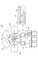
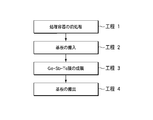
- FIG. 2 is a schematic configuration diagram showing a multi-chamber type processing system in which a plurality of film forming apparatuses of FIG. 1 are mounted. It is a flowchart for demonstrating the film-forming method of this invention.
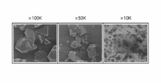
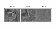
- 3 is a scanning electron micrograph showing the surface state of the film obtained in Experiment 1.
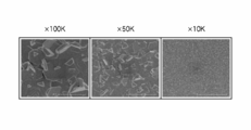
- FIG. 6 is a scanning electron micrograph showing the surface state of the film obtained in Experiment 2.
- FIG. 6 is a scanning electron micrograph showing the surface state of the film obtained in Experiment 3.
- FIG. 6 is a scanning electron micrograph showing the surface state of the film obtained in Experiment 4.
- FIG. 6 is a scanning electron micrograph showing the surface state of the film obtained in Experiment 5.
- FIG. 6 is a scanning electron micrograph showing the surface state of the film obtained in Experiment 6.
- FIG. 1 is a cross-sectional view showing a schematic configuration of a film forming apparatus that can be used in the method of forming a Ge—Sb—Te film according to the present invention.
- a film forming apparatus 100 shown in FIG. 1 has a processing container 1 formed into a cylindrical shape or a box shape by using aluminum or the like, for example.
- a mounting table 3 on which a wafer W) is mounted is provided.
- the mounting table 3 is composed of a carbon material such as a graphite plate or a graphite plate covered with SiC having a thickness of about 1 mm, ceramics having good thermal conductivity such as aluminum nitride, and the like.
- a cylindrical partition wall 13 made of, for example, aluminum, which is erected from the bottom of the processing vessel 1 is formed on the outer peripheral side of the mounting table 3, and its upper end is bent, for example, in an L shape in the horizontal direction. 14 is formed.
- the inert gas purge chamber 15 is formed on the back surface side of the mounting table 3.
- the upper surface of the bent portion 14 is substantially on the same plane as the upper surface of the mounting table 3, is separated from the outer periphery of the mounting table 3, and the connecting rod 12 is inserted through this gap.
- the mounting table 3 is supported by three (only two in the illustrated example) support arms 4 extending from the upper inner wall of the partition wall 13.
- a plurality of, for example, three L-shaped lifter pins 5 are provided so as to protrude upward from the ring-shaped support member 6.
- the support member 6 can be moved up and down by a lifting rod 7 penetrating from the bottom of the processing container 1, and the lifting rod 7 is moved up and down by an actuator 10 located below the processing container 1.
- a portion corresponding to the lifter pin 5 of the mounting table 3 is provided with an insertion hole 8 that penetrates the mounting table 3. 5 can be inserted into the insertion hole 8 to lift the wafer W.
- the insertion portion of the elevating rod 7 into the processing container 1 is covered with a bellows 9 to prevent outside air from entering the processing container 1 from the insertion portion.
- a ceramic clamp such as an aluminum nitride having a substantially ring shape along the contour of the wafer W is provided.
- a ring member 11 is provided.
- the clamp ring member 11 is connected to the support member 6 via a connecting rod 12 and is moved up and down integrally with the lifter pin 5.
- the lifter pins 5 and the connecting rods 12 are formed of ceramics such as alumina.
- a plurality of contact protrusions 16 arranged at substantially equal intervals along the circumferential direction are formed on the lower surface on the inner peripheral side of the ring-shaped clamp ring member 11, and at the time of clamping, the lower end surface of the contact protrusion 16 is The upper surface of the peripheral edge of the wafer W is brought into contact with and pressed.
- the diameter of the contact protrusion 16 is about 1 mm, and the height is about 50 ⁇ m.
- a ring-shaped first gas purge gap 17 is formed in this portion during clamping. It should be noted that the overlap amount (flow path length of the first gas purge gap 17) L1 between the peripheral edge of the wafer W and the inner peripheral side of the clamp ring member 11 during clamping is about several millimeters.
- the outer peripheral edge of the clamp ring member 11 is positioned above the upper bent portion 14 of the partition wall 13, and a ring-shaped second gas purge gap 18 is formed here.
- the width (height) of the second gas purge gap 18 is, for example, about 500 ⁇ m, and is about 10 times larger than the width of the first gas purge gap 17.
- the overlap amount between the outer peripheral edge portion of the clamp ring member 11 and the bent portion 14 (the flow path length of the second gas purge gap 18) is, for example, about 10 mm.
- An inert gas supply mechanism 19 that supplies an inert gas to the inert gas purge chamber 15 is provided at the bottom of the processing container 1.
- the gas supply mechanism 19 includes a gas nozzle 20 for introducing an inert gas such as Ar gas (backside Ar) into the inert gas purge chamber 15, and an Ar gas supply source 21 for supplying Ar gas as an inert gas.
- a gas pipe 22 for guiding Ar gas from the Ar gas supply source 21 to the gas nozzle 20.
- the gas pipe 22 is provided with a mass flow controller 23 as a flow rate controller and open / close valves 24 and 25.
- Other inert gases such as He gas may be used as the inert gas instead of Ar gas.
- a transmission window 30 made of a heat ray transmission material such as quartz is airtightly provided immediately below the mounting table 3 at the bottom of the processing container 1, and a box-shaped heating is provided below this transmission window 30 so as to surround the transmission window 30.
- a chamber 31 is provided.
- a plurality of heating lamps 32 are attached as a heating means to a turntable 33 that also serves as a reflecting mirror.
- the turntable 33 is rotated by a rotation motor 34 provided at the bottom of the heating chamber 31 via a rotation shaft. Therefore, the heat rays emitted from the heating lamp 32 pass through the transmission window 30 and irradiate the lower surface of the mounting table 3 to heat it.
- an exhaust port 36 is provided at the peripheral edge of the bottom of the processing container 1, and an exhaust pipe 37 connected to a vacuum pump (not shown) is connected to the exhaust port 36.
- the inside of the processing container 1 can be maintained at a predetermined degree of vacuum by exhausting through the exhaust port 36 and the exhaust pipe 37.
- a loading / unloading port 39 for loading / unloading the wafer W is provided on the side wall of the processing chamber 1, and the loading / unloading port 39 can be opened and closed by a gate valve G.
- the processing container 1 is connected to a transfer chamber of a processing system described later via a gate valve G.
- a shower head 40 is provided on the ceiling of the processing container 1 facing the mounting table 3 in order to introduce a source gas or the like into the processing container 1.
- the shower head 40 is made of, for example, aluminum and has a head body 41 having a disk shape having a space 41a therein.
- a gas inlet 42 is provided in the ceiling of the head body 41.
- a processing gas supply mechanism 50 that supplies a processing gas necessary for forming a Ge—Sb—Te-based film is connected to the gas inlet 42 by a pipe 51.
- a large number of gas injection holes 43 for discharging the gas supplied into the head main body 41 to the processing space in the processing container 1 are arranged on the entire bottom surface of the head main body 41, It is designed to release gas.
- a diffusion plate 44 having a large number of gas dispersion holes 45 is disposed in the space 41 a in the head main body 41 so that gas can be supplied more evenly to the surface of the wafer W.
- cartridge heaters 46 and 47 for temperature adjustment are provided in the side wall of the processing vessel 1, the side wall of the shower head 40, and the wafer facing surface where the gas injection holes 43 are arranged, respectively.
- the side wall and the shower head portion in contact with each other can be maintained at a predetermined temperature.
- the processing gas supply mechanism 50 includes a Te raw material storage unit 52 that stores Te raw material, an Sb raw material storage unit 53 that stores Sb raw material, a Ge raw material storage unit 54 that stores Ge raw material, and a gas in the processing container 1. It has a dilution gas supply source 55 that supplies a dilution gas such as argon gas for dilution, and a pretreatment gas supply source 78 that supplies a pretreatment gas for performing pretreatment.
- NH 3 gas, H 2 gas may be a possible supply configured as an additive gas for enhancing the film quality.
- the piping 51 connected to the shower head 40 includes a piping 56 extending from the Te raw material storage 52, a piping 57 extending from the Sb raw material storage 53, a piping 58 extending from the Ge raw material storage 54, and a pretreatment gas supply source 78.
- An extending pipe 81 is connected, and the dilution gas supply source 55 is connected to the pipe 51.
- the pipe 51 is provided with a mass flow controller (MFC) 60 as a flow rate controller and front and rear opening / closing valves 61 and 62.
- the pipe 58 is provided with a mass flow controller (MFC) 63 as a flow rate controller and front and rear opening / closing valves 64 and 65.
- the pipe 81 is provided with a mass flow controller (MFC) 82 as a flow rate controller and front and rear opening / closing valves 83 and 84.
- a carrier gas supply source 66 that supplies a carrier gas for bubbling Ar or the like is connected to the Te raw material reservoir 52 via a pipe 67.
- the pipe 67 is provided with a mass flow controller (MFC) 68 as a flow rate controller and front and rear opening / closing valves 69 and 70.
- a carrier gas supply source 71 for supplying a carrier gas such as Ar is also connected to the Sb raw material reservoir 53 via a pipe 72.
- the pipe 72 is provided with a mass flow controller (MFC) 73 as a flow rate controller and open / close valves 74 and 75 before and after the mass flow controller (MFC) 73.
- the Te raw material reservoir 52 and the Sb raw material reservoir 53 are provided with heaters 76 and 77, respectively.
- the Te raw material stored in the Te raw material storage unit 52 and the Sb raw material stored in the Sb raw material storage unit 53 are supplied to the processing container 1 by bubbling while being heated by the heaters 76 and 77. It has become. Further, the Ge raw material stored in the Ge raw material storage unit 54 is supplied to the processing container 1 while the flow rate is controlled by a mass flow controller (MFC) 63. Although not shown in the drawing, a heater is also provided in the piping and the mass flow controller to the processing container 1 for supplying the Ge raw material, the Sr raw material and the Ti raw material in a vaporized state.
- MFC mass flow controller
- the Ge raw material is supplied by the mass flow controller, and the Sb raw material and the Te raw material are supplied by bubbling.
- the Ge raw material may be supplied by bubbling, and the Sb raw material and the Te raw material are supplied by the mass flow controller. May be.
- the raw material in a liquid state may be supplied by being controlled by a liquid mass flow controller and vaporized by a vaporizer.
- any compound that can supply gas can be used.
- a compound having a high vapor pressure is advantageous because it is easily vaporized.
- a compound containing an alkyl group can be suitably used because it has a high vapor pressure and is inexpensive. However, it is not limited to the thing containing an alkyl group.
- Ge raw material containing an alkyl group methyl germanium Ge (CH 3 ) H 3 , tertiary butyl germanium [Ge ((CH 3 ) 3 C) H 3 ], tetramethyl germanium [Ge ( CH 3 ) 4 ], tetraethylgermanium [Ge (C 2 H 5 ) 4 ], tetradimethylaminogermanium [Ge ((CH 3 ) 2 N) 4 ] and the like.
- Sb raw material examples include triisopropylantimony [Sb (i-C 3 H 7 ) 3 ], trimethylantimony [Sb (CH 3 ) 3 ], trisdimethylaminoantimony [Sb ((CH 3 ) 2 N) 3 ] and the like can be mentioned as Te raw materials is diisopropyl tellurium [Te (i-C 3 H 7) 2], di-tert-butyl tellurium [Te (t-C 4 H ) 2], diethyl tellurium [Te (C 2 H 5) 2] , and the like.
- the preprocessing gas supplied from the preprocessing gas supply source 78 preprocesses the inside of the processing container 1 before the wafer W is loaded, before the Ge—Sb—Te film is formed.
- a gas containing at least one of Cl and F is used as the pretreatment gas.
- the gas containing at least one of Cl and F include ClF 3 gas, F 2 gas, Cl 2 gas, and the like.
- the flow rate of these gases is preferably about 200 to 1000 mL / min (sccm), or about 133 to 399 Pa in terms of partial pressure.
- ClF 3 gas is used as the pretreatment gas
- a cleaning gas for cleaning the inside of the treatment container 1 can also be used.
- an inert gas such as an Ar gas may be supplied as a dilution gas in addition to a gas containing at least one of Cl and F.
- a pipe 86 for supplying NF 3 gas is connected to the cleaning gas introduction part 85, and a remote plasma generation part 87 is provided in the pipe 86. Then, the NF 3 gas supplied through the pipe 86 is converted into plasma in the remote plasma generation unit 87 and supplied into the processing container 1, thereby cleaning the inside of the processing container 1.
- a remote plasma generation unit may be provided immediately above the shower head 40 and the cleaning gas may be supplied via the shower head 40.
- F 2 may be used instead of NF 3 , and plasmaless thermal cleaning with ClF 3 or the like may be performed without using remote plasma.
- FIG. 2 is a schematic configuration diagram showing a processing system 200 in which a plurality of film forming apparatuses 100 are mounted.
- This processing system 200 has four film forming apparatuses 100, and the processing container 1 of these film forming apparatuses 100 is connected to a transfer chamber 105 held in a vacuum via a gate valve G.
- load lock chambers 106 and 107 are connected to the transfer chamber 105 through gate valves G.
- An air loading / unloading chamber 108 is provided on the opposite side of the load lock chambers 106 and 107 from the transfer chamber 105, and a wafer W is placed on the opposite side of the loading / unloading chamber 108 from the connecting portion of the load lock chambers 106 and 107.
- Three carrier attachment ports 109, 110, and 111 for attaching the accommodable carrier C are provided.
- a transfer device 112 that carries the wafer W in and out of the processing containers 1 of the four film forming apparatuses 100 and the two load lock chambers 106 and 107 is provided.
- the transfer device 112 is provided at substantially the center of the transfer chamber 105, and has two support arms 114a and 114b that support the semiconductor wafer W at the tip of a rotatable / extensible / retractable portion 113 that can be rotated and extended. These two support arms 114a and 114b are attached to the rotation / extension / contraction section 113 so as to face opposite directions.
- a transfer device 116 for loading / unloading the wafer W into / from the carrier C and loading / unloading the wafer W into / from the load lock chambers 106 and 107 is provided.
- the transfer device 116 has an articulated arm structure, and can run on the rail 118 along the arrangement direction of the carrier C.
- the wafer W is placed on the support arm 117 at the tip thereof and transferred. I do.
- the processing system 200 includes a control unit 120, and the control unit 120 includes a process controller 121 including a microprocessor, a user interface 122, and a storage unit 123. Each component of the processing system 200 is electrically connected to the process controller 121, and these are controlled by the process controller 121.
- the process controller 121 controls the actuator 10, the lamp 32, the rotation motor 34, the valve, the mass flow controller, and the like of the film forming apparatus 100.
- the user interface 122 is connected to the process controller 121, and includes a keyboard for an operator to input commands to manage the processing system 200, a display for visualizing and displaying the operating status of the plasma processing apparatus, and the like. .
- the storage unit 123 is connected to the process controller 121, and each configuration of the processing system 200 according to a control program for realizing various processes executed by the processing system 200 under the control of the process controller 121 and processing conditions.
- a program for causing the unit to execute processing, that is, a processing recipe is stored.
- the processing recipe is stored in a storage medium in the storage unit 123.
- the storage medium may be a fixed medium such as a hard disk or a portable medium such as a CDROM, DVD, or flash memory. Moreover, you may make it transmit a recipe suitably from another apparatus via a dedicated line, for example.
- an arbitrary processing recipe is called from the storage unit 123 according to an instruction from the user interface 122 and is executed by the process controller 121, so that the processing in the processing system 200 is performed under the control of the process controller 121. That is, the transfer of the wafer W and the film forming process of the Ge—Sb—Te film in the film forming apparatus 100 are performed.
- the wafer W is loaded into one of the load lock chambers 106 and 107 by the transfer device 116 in the loading / unloading chamber 108 from the carrier C, the load lock chamber is evacuated to a standby state, and the film forming process is started.
- the pretreatment gas is introduced into the processing container 1 from the preprocessing gas supply source 78 into the processing container 1 before the wafer W is loaded.
- Pretreatment is performed by exposing the pretreatment gas into the container 1 (step 1).
- a gas containing at least one of Cl and F such as ClF 3 gas, F 2 gas, and Cl 2 gas, is used, and such a pretreatment gas is present in the treatment container 1 by this process. It becomes a state.
- the temperature at this time may be set to an appropriate temperature depending on the kind of pretreatment gas, but is preferably 250 to 450 ° C. From the viewpoint of increasing the throughput of the treatment, it is preferable that the temperature is the same as the temperature during the film formation treatment or about ⁇ 50 ° C. even if different.
- the wafer W to be film-formed may remain in the vacuum state in the load lock chamber 106 or 107 during the pretreatment in the step 1, but the support arm 114a of the transfer device 112 or It may be taken out from the load lock chamber 106 or 107 by 114b and set in a standby state.
- Step 2 the gate valve G of the pre-processed processing container 1 is opened, and the wafer W that has been waiting is loaded into the processing container 1 from the loading / unloading port 39 by the transfer device 112 of the transfer chamber 105, and the mounting table 3.
- the gate valve G is closed, the inside of the processing container 1 is evacuated and adjusted to a predetermined degree of vacuum.
- the mounting table 3 is heated in advance by heat rays emitted from the heating lamp 32 and transmitted through the transmission window 30, and the wafer W is heated by the heat.
- a Ge source gas, an Sb source gas, and a Te source gas are flowed at a predetermined flow rate in the processing container 1 to form a Ge—Sb—Te film on the wafer W (step 3).
- Ar gas is supplied as a dilution gas from the dilution gas supply source 55 at a flow rate of 100 to 500 mL / sec (sccm), and processing is performed through an exhaust port 36 and an exhaust pipe 37 by a vacuum pump (not shown).
- a vacuum pump not shown
- the pressure in the processing container 1 is adjusted to about 60 to 1330 Pa.
- the heating temperature of the wafer W is set to 200 to 500 ° C., preferably 300 to 400 ° C., for example.
- the pressure in the processing container 1 is controlled to 60 to 6650 Pa, which is the film formation pressure, and actual film formation is started.
- the pressure in the processing container 1 is adjusted by an automatic pressure controller (APC) (not shown) provided in the exhaust pipe 37.
- APC automatic pressure controller
- the Sb raw material gas is introduced into the processing container 1 from the Sb raw material storage unit 53, and the bubbling is similarly performed by flowing a predetermined flow rate of the carrier gas.
- the Te source gas is introduced from the Te source reservoir 52 into the processing vessel 1
- the Ge source gas at a predetermined flow rate is introduced into the processing vessel 1 from the Ge source reservoir 54 by the mass flow controller (MFC) 63.
- MFC mass flow controller
- the gas flow rate at this time is, for example, Ge source gas flow rate (N 2 conversion) 550 mL / min (sccm), Sb source carrier Ar gas flow rate 20 mL / min (sccm), Te source carrier Ar gas flow rate 50 mL / min (sccm) ).
- the Ge source gas, the Sb source gas, and the Te source gas may be simultaneously supplied to form a Ge—Sb—Te film, or the Ge source gas, the Sb source gas, and the Te source gas may be alternately formed.
- a Ge—Sb—Te film may be formed by supplying.
- the Ge raw material gas flow rate (in terms of N 2 ) is a measured value when the Ge gas flow rate is measured using an N 2 mass flow controller.
- the Ge raw material gas and the Sb raw material gas and the Te raw material gas are introduced into the processing container 1, these raw materials react with at least one of Cl and F to generate active chlorides and fluorides having a high vapor pressure. This promotes the formation of initial nuclei. Therefore, relatively small crystal grains are densely formed, and a continuous film having high smoothness is obtained.
- step 4 After film formation in step 3 is completed, the supply of raw materials is stopped, the inside of the processing container 1 is purged with a dilution gas, the gate valve G is opened, and the wafer W after film formation is unloaded from the processing container 1 by the transfer device 112. (Step 4). Then, the unloaded wafer W is loaded into one of the load lock chambers 106 and 107, the load lock chamber into which the wafer W is loaded is returned to atmospheric pressure, and the wafer W is stored in the carrier C by the transfer device 116. Thus, the film forming process for one wafer is completed. Such processing is continuously performed on a plurality of wafers W in the carrier C.
- the inside of the processing container 1 is Cl in a state where the wafer W that is the substrate to be processed does not exist in the processing container 1.
- F are exposed to a gas containing at least one of them, and then the wafer W is carried in, and the gaseous Ge raw material, the gaseous Sb raw material, and the gaseous Te raw material are introduced into the processing container 1.
- the raw material reacts with at least one of Cl and F to generate active chlorides and fluorides having a high vapor pressure, thereby promoting the formation of initial nuclei. For this reason, a Ge—Sb—Te film having high smoothness can be obtained.
- Tertiary butyl germanium is supplied to the processing vessel by directly controlling the vapor flow rate with a mass flow controller installed at the latter stage of the normal temperature raw material vessel, and triisopropylantimony is supplied as a carrier gas to the raw material vessel controlled at 50 ° C.
- the controlled Ar gas was supplied to the processing vessel by a bubbling method that passed through the vessel, and diisopropyl tellurium was bubbled through the vessel with Ar gas that was flow controlled as a carrier gas in a raw material vessel controlled at 35 ° C.
- the mass flow controller and the piping from the raw material container to the processing container were maintained at 160 ° C. by a mantle router.
- the present invention is not limited to the above embodiment and can be variously limited.
- the pretreatment is performed before the substrate is transported to the processing container.
- the pretreatment is performed after the substrate is transported to the processing container, and the pretreatment of the processing container and the pretreatment of the substrate are performed simultaneously. May be.
- the lifter pin is adjusted and the substrate is lifted from the mounting table, and the treatment pressure is 266 Pa or less, preferably 133 Pa or less.
- the substrate can be kept at a temperature lower by 50 to 100 ° C. than the mounting table.
- a film forming apparatus that heats a substrate to be processed by lamp heating is shown, but a film heating apparatus may be heated by a resistance heater.
- a film heating apparatus may be heated by a resistance heater.
- an example using a multi-chamber type processing system equipped with four film forming apparatuses is shown, but the number of film forming apparatuses is not particularly limited, and the number of film forming apparatuses is one. It may be individual.
- the Ge—Sb—Te film is applied to the phase change layer of the PRAM has been described. However, it can be applied to other uses such as a recording layer of a phase change type optical storage medium. Therefore, the substrate is not limited to a semiconductor substrate, and various other substrates such as a glass substrate and a resin substrate can be used.
Landscapes
- Chemical & Material Sciences (AREA)
- Engineering & Computer Science (AREA)
- General Chemical & Material Sciences (AREA)
- Chemical Kinetics & Catalysis (AREA)
- Materials Engineering (AREA)
- Mechanical Engineering (AREA)
- Metallurgy (AREA)
- Organic Chemistry (AREA)
- Inorganic Chemistry (AREA)
- Manufacturing & Machinery (AREA)
- Chemical Vapour Deposition (AREA)
Abstract
Description
また、他の目的はそのような方法を実行させるプログラムが記憶された記憶媒体を提供することにある。
ここでは、Ge-Sb-Te膜を、半導体ウエハ上にPRAMの相変化層として成膜する場合について説明する。
図1は、本発明に係るGe-Sb-Te膜の成膜方法の実施に用いることができる成膜装置の概略構成を示す断面図である。図1に示す成膜装置100は、例えばアルミニウムなどにより円筒状あるいは箱状に成形された処理容器1を有しており、処理容器1内には、被処理基板である半導体ウエハ(以下、単にウエハと記す)Wが載置される載置台3が設けられている。載置台3は厚さ1mm程度の例えばグラファイト板あるいはSiCで覆われたグラファイト板などのカーボン素材、窒化アルミニウムなどの熱伝導性の良いセラッミクス等により構成される。
<実験1>
上記図1の成膜装置において、カートリッジヒータにより処理容器壁の温度を160℃に設定し、ランプパワーを調節して、載置台の温度を360℃に設定し、搬送装置の支持アームを用いて処理容器内に直径200mmの円板状をなすウエハを搬入し、以下の条件でGe-Sb-Te膜を成膜した。なお、Ge原料、Sb原料、Te原料として、それぞれターシャリブチルゲルマニウム、トリイソプロピルアンチモン、ジイソプロピルテルルを用いた。ターシャリブチルゲルマニウムは、常温の原料容器の後段に設置したマスフローコントローラにて蒸気流量を直接制御して処理容器に供給し、トリイソプロピルアンチモンは、50℃に温度コントロールした原料容器にキャリアガスとして流量制御されたArガスを容器内に通じたバブリング法にて処理容器に供給し、ジイソプロピルテルルは、35℃に温度コントロールした原料容器にキャリアガスとして流量制御されたArガスを容器内に通じたバブリング法にて処理容器に供給した。マスフローコントローラおよび原料容器から処理容器までの配管は、マントルータにより160℃に保持した。
載置台温度:360℃
処理容器内圧力:665Pa
Ge原料ガス流量:550mL/min(sccm):ただしN2換算にて
Te原料キャリアArガス流量:50mL/min(sccm)
Sb原料キャリアArガス流量:20mL/min(sccm)
希釈Arガス流量:100mL/min(sccm)
バックサイドArガス流量:200mL/min(sccm)
成膜時間:90sec
次に、実験1と同様の装置を用い、処理容器内にウエハWとしてSiウエハを搬入するに先立って、以下の条件で処理容器内を前処理ガスに曝露させて前処理を行った後、実験1と全く同様にGe-Sb-Te膜を成膜した。
前処理条件は、以下の通りである。
載置台温度:300℃
処理容器内圧力:612Pa
前処理ガス流量
ClF3ガス流量:400mL/min(sccm)
Arガス(希釈ガス)流量:400mL/min(sccm)
処理時間:1800sec
次に、処理容器内にウエハWとしてSiO2ウエハを搬入するに先立って、以下の条件で処理容器内を前処理ガスに曝露させて前処理を行った後、実験1と全く同様にGe-Sb-Te膜を成膜した。
前処理条件は、以下の通りである。
載置台温度:360℃
処理容器内圧力:665Pa
前処理ガス流量
ClF3ガス流量:400mL/min(sccm)
Arガス(希釈ガス)流量:600mL/min(sccm)
処理時間:600sec
次に、実験3と同様、処理容器内にSiO2ウエハを搬入するに先立って、処理時間が60secである点を除いて同じ条件で処理容器内を前処理ガスに曝露させて前処理を行った後、実験1と全く同様にGe-Sb-Te膜を成膜した。
蛍光X線分析法(XRF)にて得られた膜の組成を測定した結果、Ge/Sb/Te=26/23/52(at%)となり、XRF換算膜厚は111nmであった。その表面性状は図7の走査型電子顕微鏡(SEM)写真で示すように、平滑性という観点からは実験3に劣るものとなった。これより前処理時間が長いほど、連続化が進むために平滑性が良くなり、また成膜量も増加することがわかる。
<実験5>
処理容器内にSiウエハを搬入するに先立って、ClF3ガス流量が200sccmである点を除いては実験3と同じ条件で処理容器内を前処理ガスに曝露させて前処理を行った後、実験1と全く同様の成膜条件でGe-Sb-Te膜を成膜した。
蛍光X線分析法(XRF)にて得られた膜の組成を測定した結果、Ge/Sb/Te=22/25/53(at%)となり、XRF換算膜厚は181nmであった。その表面性状は図8の走査型電子顕微鏡(SEM)写真で示すようになった。
処理容器内に搬入する被処理基板がSiO2ウエハである点のみが異なり、他は実験5と同じ条件(前処理条件、成膜条件)でGe-Sb-Te膜を成膜した。
蛍光X線分析法(XRF)にて得られた膜の組成を測定した結果、Ge/Sb/Te=20/26/54(at%)となり、XRF換算膜厚は163nmであった。その表面性状は図9の走査型電子顕微鏡(SEM)写真で示すようになった。
実験5、6の結果より、同じ前処理条件で基板を処理してもSiウエハの方がSiO2ウエハよりも膜の連続化が進み、成膜量も増加するのがわかる。
Claims (6)
- 処理容器内に基板が存在しない状態で前記処理容器内をClおよびFの少なくとも一方を含むガスに曝露させることと、
その後、前記処理容器内に基板を搬入することと、
基板が搬入された前記処理容器内に、気体状のGe原料、気体状のSb原料、および気体状のTe原料を導入してCVDにより基板上にGe2Sb2Te5となるGe-Sb-Te膜を成膜することと
を有する、Ge-Sb-Te膜の成膜方法。 - 前記処理容器内をClおよびFの少なくとも一方を含むガスに曝露させる際に、ClおよびFの少なくとも一方を含むガスとしてClF3ガスを用いる、請求項1に記載のGe-Sb-Te膜の成膜方法。
- 前記Ge-Sb-Te膜の成膜は、200~500℃の範囲の温度で行う、請求項1に記載のGe-Sb-Te膜の成膜方法。
- 前記処理容器内をClおよびFの少なくとも一方を含むガスに曝露させる際に、前記Ge-Sb-Te膜を成膜する温度の±50℃の範囲の温度で行う、請求項3に記載のGe-Sb-Te膜の成膜方法。
- Ge原料、Sb原料およびTe原料は、アルキル基を含む化合物よりなる、請求項1に記載のGe-Sb-Te膜の成膜方法。
- コンピュータ上で動作し、成膜装置を制御するプログラムが記憶された記憶媒体であって、
前記プログラムは、実行時に、処理容器内に基板が存在しない状態で前記処理容器内をClおよびFの少なくとも一方を含むガスに曝露させることと、その後、前記処理容器内に基板を搬入することと、基板が搬入された前記処理容器内に、気体状のGe原料、気体状のSb原料、および気体状のTe原料を導入してCVDにより基板上にGe2Sb2Te5となるGe-Sb-Te膜を成膜することとを有するGe-Sb-Te膜の成膜方法が行われるように、コンピュータに前記成膜装置を制御させる、記憶媒体。
Priority Applications (3)
| Application Number | Priority Date | Filing Date | Title |
|---|---|---|---|
| US13/376,749 US8372688B2 (en) | 2009-06-09 | 2010-06-02 | Method for forming Ge-Sb-Te film and storage medium |
| KR1020127000467A KR101361984B1 (ko) | 2009-06-09 | 2010-06-02 | 저마늄-안티모니-텔루륨 막의 성막 방법 및 기억 매체 |
| CN2010800252623A CN102460665A (zh) | 2009-06-09 | 2010-06-02 | Ge-Sb-Te膜的成膜方法和存储介质 |
Applications Claiming Priority (2)
| Application Number | Priority Date | Filing Date | Title |
|---|---|---|---|
| JP2009-138274 | 2009-06-09 | ||
| JP2009138274A JP2010287615A (ja) | 2009-06-09 | 2009-06-09 | Ge−Sb−Te膜の成膜方法および記憶媒体 |
Publications (1)
| Publication Number | Publication Date |
|---|---|
| WO2010143570A1 true WO2010143570A1 (ja) | 2010-12-16 |
Family
ID=43308825
Family Applications (1)
| Application Number | Title | Priority Date | Filing Date |
|---|---|---|---|
| PCT/JP2010/059337 Ceased WO2010143570A1 (ja) | 2009-06-09 | 2010-06-02 | Ge-Sb-Te膜の成膜方法および記憶媒体 |
Country Status (5)
| Country | Link |
|---|---|
| US (1) | US8372688B2 (ja) |
| JP (1) | JP2010287615A (ja) |
| KR (1) | KR101361984B1 (ja) |
| CN (1) | CN102460665A (ja) |
| WO (1) | WO2010143570A1 (ja) |
Families Citing this family (5)
| Publication number | Priority date | Publication date | Assignee | Title |
|---|---|---|---|---|
| US9157152B2 (en) * | 2007-03-29 | 2015-10-13 | Tokyo Electron Limited | Vapor deposition system |
| WO2013027682A1 (ja) * | 2011-08-19 | 2013-02-28 | 東京エレクトロン株式会社 | Ge-Sb-Te膜の成膜方法、Ge-Te膜の成膜方法、Sb-Te膜の成膜方法及びプログラム |
| JP2015183260A (ja) * | 2014-03-25 | 2015-10-22 | 株式会社日立国際電気 | クリーニング方法、基板処理装置およびプログラム |
| US10751765B2 (en) * | 2018-08-13 | 2020-08-25 | Applied Materials, Inc. | Remote plasma source cleaning nozzle for cleaning a gas distribution plate |
| US20210391156A1 (en) * | 2020-06-10 | 2021-12-16 | Applied Materials, Inc. | Clean unit for chamber exhaust cleaning |
Citations (3)
| Publication number | Priority date | Publication date | Assignee | Title |
|---|---|---|---|---|
| JP2007258440A (ja) * | 2006-03-23 | 2007-10-04 | Hitachi High-Technologies Corp | プラズマ処理方法 |
| JP2008103731A (ja) * | 2006-10-20 | 2008-05-01 | Samsung Electronics Co Ltd | 相変化メモリ素子の製造方法及びこれに適用された相変化層の形成方法 |
| JP2008159787A (ja) * | 2006-12-22 | 2008-07-10 | Tokyo Electron Ltd | 真空装置のクリーニング方法、真空装置の制御装置および制御プログラムを記憶した記憶媒体 |
Family Cites Families (7)
| Publication number | Priority date | Publication date | Assignee | Title |
|---|---|---|---|---|
| US20060172067A1 (en) * | 2005-01-28 | 2006-08-03 | Energy Conversion Devices, Inc | Chemical vapor deposition of chalcogenide materials |
| KR100688532B1 (ko) * | 2005-02-14 | 2007-03-02 | 삼성전자주식회사 | 텔루르 전구체, 이를 이용하여 제조된 Te-함유 칼코게나이드(chalcogenide) 박막, 상기 박막의 제조방법 및 상변화 메모리 소자 |
| EP2018642A4 (en) * | 2006-05-12 | 2009-05-27 | Advanced Tech Materials | LOW TEMPERATURE DEPOSITION OF STORAGE MATERIALS |
| KR20080026746A (ko) * | 2006-09-21 | 2008-03-26 | 삼성전자주식회사 | 증착 챔버 세정 방법 |
| US20080154410A1 (en) | 2006-12-22 | 2008-06-26 | Tokyo Electron Limited | Method for cleaning vacuum apparatus, device for controlling vacuum apparatus, and computer-readable storage medium storing control program |
| US7704895B2 (en) * | 2008-04-02 | 2010-04-27 | Intel Corporation | Deposition method for high-k dielectric materials |
| KR101580575B1 (ko) * | 2008-04-25 | 2015-12-28 | 에이에스엠 인터내셔널 엔.브이. | 텔루르와 셀렌 박막의 원자층 증착을 위한 전구체의 합성과 그 용도 |
-
2009
- 2009-06-09 JP JP2009138274A patent/JP2010287615A/ja active Pending
-
2010
- 2010-06-02 US US13/376,749 patent/US8372688B2/en active Active
- 2010-06-02 KR KR1020127000467A patent/KR101361984B1/ko active Active
- 2010-06-02 WO PCT/JP2010/059337 patent/WO2010143570A1/ja not_active Ceased
- 2010-06-02 CN CN2010800252623A patent/CN102460665A/zh active Pending
Patent Citations (3)
| Publication number | Priority date | Publication date | Assignee | Title |
|---|---|---|---|---|
| JP2007258440A (ja) * | 2006-03-23 | 2007-10-04 | Hitachi High-Technologies Corp | プラズマ処理方法 |
| JP2008103731A (ja) * | 2006-10-20 | 2008-05-01 | Samsung Electronics Co Ltd | 相変化メモリ素子の製造方法及びこれに適用された相変化層の形成方法 |
| JP2008159787A (ja) * | 2006-12-22 | 2008-07-10 | Tokyo Electron Ltd | 真空装置のクリーニング方法、真空装置の制御装置および制御プログラムを記憶した記憶媒体 |
Also Published As
| Publication number | Publication date |
|---|---|
| KR20120027484A (ko) | 2012-03-21 |
| KR101361984B1 (ko) | 2014-02-11 |
| US8372688B2 (en) | 2013-02-12 |
| JP2010287615A (ja) | 2010-12-24 |
| US20120108005A1 (en) | 2012-05-03 |
| CN102460665A (zh) | 2012-05-16 |
Similar Documents
| Publication | Publication Date | Title |
|---|---|---|
| JP6289908B2 (ja) | Ge−Sb−Te膜の成膜方法、Sb−Te膜の成膜方法及びプログラム | |
| US8252410B2 (en) | Ceramic cover wafers of aluminum nitride or beryllium oxide | |
| US9735007B2 (en) | Method of processing substrate, substrate processing apparatus, and recording medium | |
| KR102584230B1 (ko) | 성막 장치 및 성막 방법 | |
| US20220356580A1 (en) | Substrate processing apparatus, method of manufacturing semiconductor device and non-transitory computer-readable recording medium | |
| WO2010143570A1 (ja) | Ge-Sb-Te膜の成膜方法および記憶媒体 | |
| JP5346699B2 (ja) | Ge−Sb−Te膜の成膜方法および記憶媒体、ならびにPRAMの製造方法 | |
| JP5649894B2 (ja) | Ge−Sb−Te膜の成膜方法 | |
| JP2007146252A (ja) | 熱処理方法、熱処理装置及び記憶媒体 | |
| JP7195190B2 (ja) | 成膜方法および成膜装置 | |
| JP5411512B2 (ja) | Ge−Sb−Te系膜の成膜方法および記憶媒体 | |
| JP2020057769A (ja) | 半導体装置の製造方法、プログラム、及び基板処理装置 | |
| WO2019188128A1 (ja) | 半導体装置の製造方法、基板処理装置およびプログラム | |
| JP5913463B2 (ja) | Ge−Sb−Te膜の成膜方法 | |
| JP6306386B2 (ja) | 基板処理方法、基板処理装置およびプログラム | |
| JP4804636B2 (ja) | 成膜方法 | |
| US11538678B2 (en) | Deposition method | |
| JP2015183260A (ja) | クリーニング方法、基板処理装置およびプログラム | |
| US20230374656A1 (en) | Filling method and film forming apparatus | |
| TW202530463A (zh) | 氣體供給方法、半導體裝置之製造方法、基板處理裝置及程式和流量控制器 |
Legal Events
| Date | Code | Title | Description |
|---|---|---|---|
| WWE | Wipo information: entry into national phase |
Ref document number: 201080025262.3 Country of ref document: CN |
|
| 121 | Ep: the epo has been informed by wipo that ep was designated in this application |
Ref document number: 10786101 Country of ref document: EP Kind code of ref document: A1 |
|
| DPE1 | Request for preliminary examination filed after expiration of 19th month from priority date (pct application filed from 20040101) | ||
| NENP | Non-entry into the national phase |
Ref country code: DE |
|
| ENP | Entry into the national phase |
Ref document number: 20127000467 Country of ref document: KR Kind code of ref document: A |
|
| WWE | Wipo information: entry into national phase |
Ref document number: 13376749 Country of ref document: US |
|
| 122 | Ep: pct application non-entry in european phase |
Ref document number: 10786101 Country of ref document: EP Kind code of ref document: A1 |