WO2010128546A1 - 半導体装置及びその製造方法 - Google Patents
半導体装置及びその製造方法 Download PDFInfo
- Publication number
- WO2010128546A1 WO2010128546A1 PCT/JP2009/058641 JP2009058641W WO2010128546A1 WO 2010128546 A1 WO2010128546 A1 WO 2010128546A1 JP 2009058641 W JP2009058641 W JP 2009058641W WO 2010128546 A1 WO2010128546 A1 WO 2010128546A1
- Authority
- WO
- WIPO (PCT)
- Prior art keywords
- heat treatment
- junction
- layer
- region
- source
- Prior art date
- Legal status (The legal status is an assumption and is not a legal conclusion. Google has not performed a legal analysis and makes no representation as to the accuracy of the status listed.)
- Ceased
Links
Images











Classifications
-
- H—ELECTRICITY
- H10—SEMICONDUCTOR DEVICES; ELECTRIC SOLID-STATE DEVICES NOT OTHERWISE PROVIDED FOR
- H10D—INORGANIC ELECTRIC SEMICONDUCTOR DEVICES
- H10D84/00—Integrated devices formed in or on semiconductor substrates that comprise only semiconducting layers, e.g. on Si wafers or on GaAs-on-Si wafers
- H10D84/01—Manufacture or treatment
- H10D84/0123—Integrating together multiple components covered by H10D12/00 or H10D30/00, e.g. integrating multiple IGBTs
- H10D84/0126—Integrating together multiple components covered by H10D12/00 or H10D30/00, e.g. integrating multiple IGBTs the components including insulated gates, e.g. IGFETs
- H10D84/0165—Integrating together multiple components covered by H10D12/00 or H10D30/00, e.g. integrating multiple IGBTs the components including insulated gates, e.g. IGFETs the components including complementary IGFETs, e.g. CMOS devices
- H10D84/017—Manufacturing their source or drain regions, e.g. silicided source or drain regions
-
- H—ELECTRICITY
- H10—SEMICONDUCTOR DEVICES; ELECTRIC SOLID-STATE DEVICES NOT OTHERWISE PROVIDED FOR
- H10D—INORGANIC ELECTRIC SEMICONDUCTOR DEVICES
- H10D30/00—Field-effect transistors [FET]
- H10D30/01—Manufacture or treatment
- H10D30/021—Manufacture or treatment of FETs having insulated gates [IGFET]
- H10D30/0212—Manufacture or treatment of FETs having insulated gates [IGFET] using self-aligned silicidation
-
- H—ELECTRICITY
- H10—SEMICONDUCTOR DEVICES; ELECTRIC SOLID-STATE DEVICES NOT OTHERWISE PROVIDED FOR
- H10D—INORGANIC ELECTRIC SEMICONDUCTOR DEVICES
- H10D30/00—Field-effect transistors [FET]
- H10D30/01—Manufacture or treatment
- H10D30/021—Manufacture or treatment of FETs having insulated gates [IGFET]
- H10D30/0223—Manufacture or treatment of FETs having insulated gates [IGFET] having source and drain regions or source and drain extensions self-aligned to sides of the gate
- H10D30/0227—Manufacture or treatment of FETs having insulated gates [IGFET] having source and drain regions or source and drain extensions self-aligned to sides of the gate having both lightly-doped source and drain extensions and source and drain regions self-aligned to the sides of the gate, e.g. lightly-doped drain [LDD] MOSFET or double-diffused drain [DDD] MOSFET
-
- H—ELECTRICITY
- H10—SEMICONDUCTOR DEVICES; ELECTRIC SOLID-STATE DEVICES NOT OTHERWISE PROVIDED FOR
- H10D—INORGANIC ELECTRIC SEMICONDUCTOR DEVICES
- H10D30/00—Field-effect transistors [FET]
- H10D30/60—Insulated-gate field-effect transistors [IGFET]
- H10D30/601—Insulated-gate field-effect transistors [IGFET] having lightly-doped drain or source extensions, e.g. LDD IGFETs or DDD IGFETs
-
- H—ELECTRICITY
- H10—SEMICONDUCTOR DEVICES; ELECTRIC SOLID-STATE DEVICES NOT OTHERWISE PROVIDED FOR
- H10D—INORGANIC ELECTRIC SEMICONDUCTOR DEVICES
- H10D64/00—Electrodes of devices having potential barriers
- H10D64/01—Manufacture or treatment
- H10D64/011—Manufacture or treatment of electrodes ohmically coupled to a semiconductor
- H10D64/0111—Manufacture or treatment of electrodes ohmically coupled to a semiconductor to Group IV semiconductors
- H10D64/0112—Manufacture or treatment of electrodes ohmically coupled to a semiconductor to Group IV semiconductors using conductive layers comprising silicides
-
- H—ELECTRICITY
- H10—SEMICONDUCTOR DEVICES; ELECTRIC SOLID-STATE DEVICES NOT OTHERWISE PROVIDED FOR
- H10D—INORGANIC ELECTRIC SEMICONDUCTOR DEVICES
- H10D84/00—Integrated devices formed in or on semiconductor substrates that comprise only semiconducting layers, e.g. on Si wafers or on GaAs-on-Si wafers
- H10D84/01—Manufacture or treatment
- H10D84/0123—Integrating together multiple components covered by H10D12/00 or H10D30/00, e.g. integrating multiple IGBTs
- H10D84/0126—Integrating together multiple components covered by H10D12/00 or H10D30/00, e.g. integrating multiple IGBTs the components including insulated gates, e.g. IGFETs
- H10D84/0165—Integrating together multiple components covered by H10D12/00 or H10D30/00, e.g. integrating multiple IGBTs the components including insulated gates, e.g. IGFETs the components including complementary IGFETs, e.g. CMOS devices
- H10D84/0172—Manufacturing their gate conductors
- H10D84/0174—Manufacturing their gate conductors the gate conductors being silicided
-
- H—ELECTRICITY
- H10—SEMICONDUCTOR DEVICES; ELECTRIC SOLID-STATE DEVICES NOT OTHERWISE PROVIDED FOR
- H10D—INORGANIC ELECTRIC SEMICONDUCTOR DEVICES
- H10D84/00—Integrated devices formed in or on semiconductor substrates that comprise only semiconducting layers, e.g. on Si wafers or on GaAs-on-Si wafers
- H10D84/01—Manufacture or treatment
- H10D84/02—Manufacture or treatment characterised by using material-based technologies
- H10D84/03—Manufacture or treatment characterised by using material-based technologies using Group IV technology, e.g. silicon technology or silicon-carbide [SiC] technology
- H10D84/038—Manufacture or treatment characterised by using material-based technologies using Group IV technology, e.g. silicon technology or silicon-carbide [SiC] technology using silicon technology, e.g. SiGe
Definitions
- the present invention relates to a semiconductor device having a field effect transistor and a method of manufacturing the same.
- the threshold voltage decreases (short channel effect). If an element different from the intended threshold voltage is formed at the time of designing a semiconductor circuit, the element operation different from the intention of the design is caused and the function of the entire circuit is impaired. Furthermore, since the threshold voltage depends on the processing dimensions of the gate electrode, even a slight processing deviation makes it impossible to obtain an element of the intended characteristics, and a semiconductor circuit requiring a large number of uniform elements, for example, DRAM It is extremely inconvenient for manufacturing (Dynamic Random Access Memory).
- Such a short channel effect is due to the fact that the distortion of the electric field in the source and drain electrode portions of the MOSFET affects the vicinity of the center of the channel portion as the channel length is reduced. This effect can be avoided by moving the junction position of the pn junction forming the source and drain closer to the semiconductor surface (that is, making the pn junction “shallow.”) However, if the pn-junction is simply made shallow, The resistance of the source and drain electrodes increases, which impedes high-speed transmission of signals traveling through the device.
- a part of the upper part of the source and drain regions is compounded (silicided) with metal.
- Elements such as Co, Ti, and Ni are used as metal species for performing the silicide.
- the metal species for silicidation that can be compatible with the miniaturized LSI is Ni.
- the metal compound reaction (silicidation reaction) between Si and Ni can be carried out at 450 ° C. lower than 800 ° C. which is the formation temperature of CoSi 2 , and at this time a phase called NiSi, which is a low electric resistance phase, is formed.
- NiSi phase When the NiSi phase is further subjected to heat treatment at a high temperature, it is transformed to a final phase called NiSi 2 having a high electrical resistance at around 750 ° C., but a low resistivity NiSi phase is used for LSI.
- Non-Patent Document 1 shows that even with such a silicide of the NiSi phase, Ni atoms readily diffuse in the silicon forming the source and drain regions to form a shallow pn junction with the heat treatment after the formation of the silicide, and the junction is easily formed. It will reach to. For this reason, it is known that a significant junction leak current is provided (see, for example, Non-Patent Document 1).
- the present invention has been made in consideration of the above circumstances, and provides a semiconductor device which is silicided while maintaining the shallow junction positions of the source and the drain and whose junction leak current is as small as possible, and a method of manufacturing the same. .
- a semiconductor device includes a silicon semiconductor layer, a source region and a drain region provided apart from the silicon semiconductor layer, and the silicon semiconductor layer between the source region and the drain region.
- (111) has a gate insulating film provided thereon, a gate electrode provided on the gate insulating film, and a Pt-containing NiSi phase provided on the source region and the drain region.
- (102) and a silicide layer strongly oriented.
- a method of manufacturing a semiconductor device comprising: a silicide layer having a contained NiSi phase, wherein a depth D from a lower surface of the silicide layer to a junction plane where the source and drain regions form the semiconductor layer is
- the present invention it is possible to provide a semiconductor device which is silicided while maintaining the shallow junction position of the source and the drain, and the junction leak current is as small as possible, and a method of manufacturing the same.
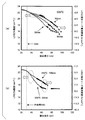
- FIGS. 1 (a) and 1 (b) are diagrams showing the pn junction depth dependency of junction leakage current and the concentration of Ni contained in a Si substrate when various heat treatments are performed after the formation of NiSi.
- FIG. 2 is a diagram of measurement of orientation of crystal grains constituting a Pt-containing silicide film and a Pt-free silicide film using XRD.
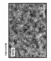
- FIG. 3 is a photograph showing a flat HAADF image of a Pt-containing NiSi film.
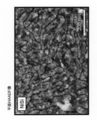
- FIG. 4 is a photograph showing a flat HAADF image of a Pt-free NiSi film.
- FIG. 5 is a diagram showing Pt concentration at each point of a Pt-containing NiSi film obtained by EDX.
- FIG. 1 (a) and 1 (b) are diagrams showing the pn junction depth dependency of junction leakage current and the concentration of Ni contained in a Si substrate when various heat treatments are performed after the formation of NiSi.
- FIG. 2 is a diagram of measurement of
- FIG. 6 is a photograph showing a cross-sectional HAADF image of a Pt-containing NiSi film.
- FIG. 7 is a schematic view for explaining the origin of change in orientation of crystal grains, addition of a specific network of Pt in the form of a specific network, and improvement in heat resistance.
- FIGS. 8 (a) and 8 (b) show the pn junction depth dependency of the junction leakage current density and the concentration of Ni contained in the Si substrate, which were observed when heat treatment was not performed after silicidation.
- FIG. 9 is a diagram showing the junction leak current density of NiSi formed by solid phase diffusion of As and the pn junction depth dependency of the concentration of Ni contained in the Si substrate.
- FIG. 10 is a graph showing the pn junction depth dependency of junction leakage current density when heat treatment at 500 ° C. is performed after formation of Pt-containing NiSi.
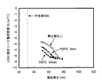
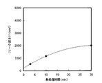
- FIG. 11 is a diagram showing the square of the leak depth caused by the initial leak current as a function of heat treatment time.
- FIG. 12 is a diagram showing the logarithm of the reduction rate of the initial leak current due to the heat treatment at 500 ° C. and 550 ° C. as the reciprocal of the absolute temperature.
- FIG. 13 is a view schematically showing the concept of effective heat treatment and excess heat treatment capable of reducing the total junction leak current.
- 14 (a) to 14 (c) are diagrams showing the square of the leak depth when heat treatment at 550 ° C., 650 ° C. and 700 ° C.
- FIG. 16 is a diagram showing the square of the leak depth when forming a NiSi after ion implantation of F on the n + / p junction and subjecting this to heat treatment as a function of the heat treatment time.
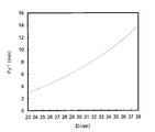
- FIG. 17 shows F 1 ⁇ 1 as a function of D.
- FIG. 18 shows F 2 ⁇ 1 as a function of D.
- FIG. 19 shows F 3 ⁇ 1 as a function of D.
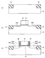
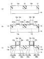
- 20 (a) to 20 (c) are cross-sectional views showing the method for manufacturing the semiconductor device according to the first embodiment.
- 21 (a) to 21 (c) are cross-sectional views showing the method for manufacturing the semiconductor device according to the first embodiment.
- 22 (a) to 22 (b) are cross-sectional views showing the method for manufacturing the semiconductor device according to the first embodiment.
- FIG. 23 is a cross-sectional view showing the method of manufacturing the semiconductor device according to the first embodiment;
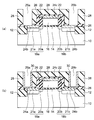
- 24 (a) to 24 (c) are cross-sectional views showing a method of manufacturing a semiconductor device according to the second embodiment.
- 25 (a) to 25 (c) are cross-sectional views showing the method for manufacturing the semiconductor device according to the second embodiment.
- FIG. 26 is a cross-sectional view showing the method of manufacturing the semiconductor device according to the second embodiment.
- the inventors of the present invention have found that the junction leak current resulting from the formation of silicide includes the junction leak current caused by the high-speed diffusion of metal atoms forming the silicide accompanying the heat treatment after the formation of silicide. It has been found that there is a junction leak current derived from the silicidation reaction itself, which is completely different from the physical origin.
- the junction leakage current derived from the silicidation reaction itself is performed by performing the heat treatment under the above heat treatment conditions, that is, at the predetermined temperature and longer than the predetermined time.
- NiSi phase exhibits extremely thermally unstable behavior long before the silicide of the NiSi phase undergoes a phase transition reaction.
- the present inventors prepare a Si substrate having pn junctions of various depths formed by solid phase diffusion of B, deposit Ni or Ni containing 5 atomic% of Pt on this, and then in a nitrogen atmosphere Then, RTA (Rapid Thermal Annealing) treatment was performed at 450 ° C. for 30 seconds to form NiSi or NiSi containing Pt (hereinafter also referred to as Pt containing NiSi) to a thickness of about 30 nm. Thereafter, heat treatment at 500 ° C. or 550 ° C. was applied.
- RTA Rapid Thermal Annealing
- FIG. 1 (a) heat treatment was applied after forming NiSi, and the observed junction leak current density (right vertical scale) was determined as a function of the pn junction depth and using the back surface SIMS method.
- FIG. 1 (b) is a diagram showing, in a corresponding manner, the depth distribution of the concentration (left vertical scale) of Ni contained in the Si substrate of the sample of FIG. After that, heat treatment is applied, and the observed junction leak current density (right vertical scale) is a function of the pn junction depth, and Ni contained in the Si substrate of each sample obtained using the back surface SIMS method
- FIG. 7 is a diagram showing, in a corresponding form, the depth distribution of the concentration (the left vertical scale) of FIG.
- junction depth distribution of junction leakage current density and the depth distribution of Ni concentration match extremely well, and it is believed that the origin of the occurrence of this leakage current is due to Ni diffused into the Si substrate along with the heat treatment. , There is no doubt.
- FIG. 2 shows the results of measurement of the orientation of crystal grains of a Pt-containing NiSi film and a NiSi film not containing the film using XRD (X-ray diffraction).
- the generated silicide becomes Ni x Pt 1-x Si in which a part of Ni in the NiSi phase is replaced by Pt, but note that the crystal structure basically does not change Do.
- the crystal grains when not containing Pt, the crystal grains mainly orient the crystal face (020) or (013) in the vertical direction.
- the orientation of the crystal grains produced from Ni containing 5 atomic% of Pt mainly orients the crystal face (111) or (102) in the vertical direction, 111)
- strong orientation to (111) or (102) means that (111) or (102) plane is the largest area when the crystal planes parallel to the Si substrate of each crystal grain forming the silicide layer are counted. Means greater.
- planar HAADF High angle annular dark field images of a NiSi film containing Pt and a NiSi film not containing Pt are shown in FIGS. 3 and 4, respectively. Note that in this method, heavy atoms or dense areas are perceived as white contrast. It should also be noted that although contrast is adjusted for each measurement, relative comparison of contrast within one image is possible, but contrast between each HAADF image of different measurements can not be compared directly.
- FIG. 3 it can be seen that in the case of Pt-containing NiSi produced from a NiPt alloy to which 5 atomic% of Pt is added, a white mesh-like structure appears. And, quite characteristically, this white mesh-like structure does not correspond to grain boundaries. Grain boundaries are indicated by very fine dark lines, ie very fine lines as compared to NiSi without Pt. It should also be noted that the dark, low density grain boundaries have apparently disappeared, as in the case of NiSi which does not contain Pt.
- white mesh nodes three points, typically as shown as point 1 in FIG. 3
- white mesh networks Five points on each side (typically, a point as indicated by point 3 in FIG. 3), and a white mesh interior point (typically, a point as indicated by point 2 in FIG. 3)
- the concentration (atomic%) of Pt detected as a result of random extraction and analysis of the elemental composition by EDX (Energy dispersive X-ray spectrometry) is shown in FIG.
- EDX Electrodegy dispersive X-ray spectrometry
- FIG. 6 shows the results of an attempt to investigate the cross section HAADF in order to investigate the uneven distribution of Pt in the silicide film thickness direction. Further, FIG. 6 also shows the composition analysis points (point 1 to point 5) by EDX and the concentrations of Pt detected at the respective points.
- the white network is localized near the center of the silicide film, and it can be seen that Pt, which is higher than the Pt concentration of the original NiPt alloy, is concentrated here.
- Pt which is higher than the Pt concentration of the original NiPt alloy
- the Pt concentration is 0.7 atomic% (that is, Pt of the original NiPt alloy An area of 14% of the concentration was found to be present.
- NiSi phase When Ni is formed on Si and heat treatment is applied thereto, the NiSi phase does not suddenly appear. Intermediately, a Ni-rich phase such as Ni 2 Si is formed, and this phase is rapidly transformed to the NiSi phase.
- a network-like region is formed in which Pt is accumulated at a Pt concentration or more of the NiPt alloy inside a NiSi phase crystal grain which is neither a grain boundary nor an interface with the Si substrate nor a silicide surface.
- the presence of Pt localized at grain boundaries of the mesophase modulates the orientation of the mesophase itself and the subsequent phase transition to the NiSi phase.
- the phase transition rate may be reduced, and it may be changed to NiSi while retaining the influence of the orientation of the mesophase. It is believed that this ultimately changes the orientation of the Pt-containing NiSi phase and causes strong orientation to (111) or (102).
- NiSi crystal grains strongly oriented to (111) or (102) on Si form a more stable interface structure with Si. Since Pt does not accumulate specifically at the interface, the origin of the improvement of heat resistance by the addition of Pt is stable due to such change in the orientation of NiSi crystal grains, that is, Ni infiltrates into the Si substrate It is presumed to be the appearance of a difficult interface structure.
- At least at least 0.7 atomic% of Pt is contained in the Pt-containing NiSi phase produced from the NiPt alloy to which 5 atomic% or more and 10 atomic% or less of Pt is added.
- Pt having a maximum of about 24 atomic%, which is twice the maximum value (12 atomic%) when 5 atomic% of Pt is uniformly added, is present.
- a high concentration Pt region and a low concentration Pt region are formed in the NiSi phase, and the Pt concentration at a certain point in the high concentration Pt region exceeds twice the Pt concentration at a certain point in the low concentration Pt region It will be.
- junction leak current caused by silicide includes junction leak current caused by high-speed diffusion of metal atoms that form silicide accompanying heat treatment after silicide formation described above. It was discovered that there is a junction leak current derived from the silicidation reaction itself, which is completely different from the physical origin.
- FIGS. 8 (a) and 8 (b) show the junction leakage current density (right vertical scale) observed when the above junction is not heat treated after silicidation as a function of the pn junction depth. Also, the depth distribution of the concentration (left vertical scale) of Ni contained in the Si substrate of each sample determined using the back surface SIMS method is shown together in a corresponding manner.
- FIG. 8 (a) shows data of NiSi
- FIG. 8 (b) shows Pt-containing NiSi data.
- the junction depth distribution of the junction leakage current density and the depth distribution of the concentration of Ni do not match, and the origin of this leakage current generation is Si along with the heat treatment. It became clear that this was not due to Ni diffused into the substrate. Further, it is needless to say that the involvement of Pt atoms is also denied because this initial leak current is generated regardless of the presence or absence of Pt.
- junction depth distribution of junction leakage current density and the depth distribution of Ni concentration match extremely well, and there is no occurrence of abnormal junction leakage at the deep portion of the Si substrate without Ni infiltration. Recognize. That is, it was also revealed that this initial leak specifically occurs at the p + / n junction including the high concentration B layer.
- B is specifically involved in the generation of the initial leak current, the physical origin of the initial leak current is the defect of Si itself and the compound defect of B. What has a stable structure as a composite defect of Si itself and B is called a boron interstitial cluster (hereinafter also referred to as BIC, ⁇ Boron Interstitial Cluster ⁇ ).
- the physical origin of the initial leak is considered to be BIC in which B is complexed with the defect of Si itself induced by the silicidation reaction.
- FIG. 10 shows the junction leakage current density (right vertical scale) when heat treatment at 500 ° C. was applied to the junction where the Pt-containing NiSi film was formed, and the case where heat treatment was not performed after silicidation was observed.
- the junction leakage current density is shown as a function of pn junction depth.
- the initial junction leak current derived from the silicidation reaction itself is rapidly reduced by the heat treatment at 500.degree.
- this heat treatment it is also understood that the diffusion of Ni atoms from the NiSi film whose heat resistance is improved by the inclusion of Pt is suppressed, and the junction leakage can be reduced. That is, the existence of heat treatment conditions capable of reducing the initial junction leak current derived from the silicidation reaction itself without causing high-speed diffusion of metal atoms has been exemplarily proved.
- BIC is not decomposed by heat treatment at about 500 ° C., but it is possible to change the internal structure and change the position of energy levels. From the viewpoint of the leak current source, if the level located at the center of the band gap (about 1.1 eV) of silicon moves to the band edge, the leak current generation capability is lost. That is, the leak current source is effectively eliminated thermally.
- the activation energy E a of about half the band gap of silicon obtained above is considered to reflect such a circumstance.
- the leak depth D 1 (nm) of the initial junction leak current derived from the silicidation reaction itself is The heat treatment temperature T a (K: absolute temperature), Heat treatment time ⁇ a (min) Heat treatment by It can be seen that it decreases exponentially as follows.
- ⁇ 1 is an effective heat treatment time defined as follows.
- equation (A2) uses the activation energy E a and the physical behavior at the general heat treatment temperature T a Procedure to guide the Note that similar procedures are also used below.
- FIGS. 1A and 1B show that the heat resistance of the silicide film is improved by the inclusion of Pt on the p + / n junction. Therefore, by utilizing the Pt-containing NiSi film, the junction leak current derived from the silicidation reaction itself can be reduced without causing high-speed diffusion of metal atoms.
- RTA treatment is performed in a nitrogen atmosphere to form Pt-containing NiSi to a thickness of about 30 nm, and then heat treatment at 550 ° C., 650 ° C., and 700 ° C.
- the square of the leak depth when performed is shown in FIGS. 14A to 14C as a function of the heat treatment time. There was no difference in the content of Pt between the samples of 5 atomic% to 10 atomic%.
- FIGS. 14 (a) to 14 (c) The linear time dependence in FIGS. 14 (a) to 14 (c) shows that the dynamics of the infiltration of the leak source (Ni atom) into the silicon substrate is the initial burst amount (offset of the graph at heat treatment time 0). (Equivalent) and the diffusion process (linear part of the graph) show that it can be formulated.
- the initial burst amount and the effective diffusion coefficient are shown in FIGS. 15 (a) and 15 (b) as a function of the heat treatment temperature. Show.
- the initial burst amount at 650 ° C. or less is 22.73 nm
- the effective diffusion constant at 550 ° C. is 7.067 nm 2 / min.
- ⁇ 2 is an effective heat treatment time defined as follows.
- a Pt-containing NiSi phase produced from a NiPt alloy to which 5 atomic% or more and 10 atomic% or less of Pt is added contains at least 0.7 atomic% or more of Pt, and a high concentration area contains 24 atomic% at maximum. Note that some degree of Pt will be present.
- ion implantation of F is performed under the conditions of a dose of 1.0 ⁇ 10 14 cm ⁇ 2 and acceleration energy of 2 keV on the n + / p junction to form NiSi.
- the square of the leak depth upon heat treatment at 500 ° C. is shown as a function of heat treatment time.
- the initial stage of the heat treatment can be approximated by the initial burst and the subsequent diffusion process, but the effective diffusion constant decreases with time due to the gettering effect of F or the like. Considering the time dependence of the effective diffusion constant up to the first order, it is as follows.
- ⁇ 3 is an effective heat treatment time defined as follows.
- the various heat treatments (temperature raising steps) applied after silicide formation are indicated by the symbol i (1 ⁇ i ⁇ n), and the heat treatment conditions are respectively the absolute temperature T ai [K] and the heat treatment time ⁇ ai [min]
- T ai [K] the total effective heat treatment time ⁇ 2e
- F 2 -1 indicates an inverse function of the function F 2 shown in the equation (B1).
- the total junction leak on the n + / p junction can be sufficiently reduced without causing high-speed diffusion of metal atoms.
- the upper limit can be defined as a function of the junction depth D.
- F 1 -1 indicates the inverse function of the function F 1 shown in the equation (A1).
- the inverse function F 1 -1 is shown as a function of D in FIG. 17 for reference.
- the inverse function F 2 -1 is shown as a function of D in FIG. 18 for reference.
- the type 3 effective heat treatment time ⁇ 3e When we define ⁇ 3 e ⁇ F 3 ⁇ 1 (D) (type 3 conditions)
- the inverse function F 3 -1 is shown as a function of D for reference in FIG.
- the junction leak current derived from the silicidation reaction itself is reduced, and moreover, it is caused by the high-speed diffusion of metal atoms.
- the generation of junction leakage current can be suppressed, and the range of heat treatment conditions that can reduce the total junction leakage current can be determined.
- the present embodiment suppresses the diffusion of Ni atoms into the substrate, reduces the junction leak current derived from the silicidation reaction itself, and is silicided while maintaining the shallow junction position of the source and the drain, and the junction leak. It embodies a simple method of manufacturing a P-MOSFET structure with a current as small as possible.
- an n-type silicon semiconductor substrate (or semiconductor layer) 10 is prepared, and first, lithography technology and RIE (Reactive Ion Etching) are used to separate element regions in which elements are formed.
- a shallow groove is formed on the surface of the semiconductor substrate 10.
- the groove is filled with an insulating material such as a silicon oxide film to the substrate surface using, for example, a CVD (Chemical Vapor Deposition) method, and planarized using, for example, a CMP (Chemical Mechanical Polishing) method.
- CVD Chemical Vapor Deposition
- CMP Chemical Mechanical Polishing
- a thermal oxide film having a thickness of, for example, 5 nm is formed on the substrate 10 as the gate insulating film 14 using a known technique such as a thermal oxidation method.
- a polysilicon film having a thickness of, for example, 200 nm is deposited as the gate electrode 16 using a known technique such as, for example, a CVD method.
- a photoresist (not shown) is applied on the gate electrode 16, and a mask made of photoresist is formed using a lithography technique. Using this mask, the gate electrode 16 and the gate insulating film 14 are processed into a gate shape, for example, by the RIE method.
- shallow diffusion layers 20a and 20b having a p-type conductivity and serving as the extension regions of the source and the drain are formed in the left and right substrates 10 of the gate electrode 16 by ion implantation of B. .
- a silicon nitride film is deposited on one surface to a thickness of 20 nm by, for example, a CVD method, and thereafter anisotropic etching such as an RIE step is added to form silicon on the side surfaces of the gate electrode 16.
- a nitride film is selectively left to form gate sidewalls 22.
- deep diffusion layers 21a and 21b having a junction depth with p-type conductivity are formed in the left and right substrates 10 of the gate electrode 16 by ion implantation of B respectively.
- the diffusion layers 20a and 21a become source regions 18a, and the diffusion layers 20b and 21b become drain regions 18b.
- B is also injected into the electrode 16.
- rapid thermal processing is performed to activate the impurities in the source and drain regions 18a and 18b.
- Diffusion layers 21 a and 21 b are formed to a depth of, for example, 47 nm from the surface of silicon semiconductor substrate 10.
- a Ni film 24 containing 5 atomic% or more and 10 atomic% or less of Pt is deposited on the entire surface to a film thickness of 12 nm, for example, using a known technique such as sputtering. Do. If necessary, a metal layer to be a cap layer (not shown) may be further formed thereon, for example, a layer such as a Ti layer or a TiN layer.
- the semiconductor substrate is subjected to rapid thermal processing in nitrogen under conditions of, for example, 450 ° C. and 30 seconds to selectively advance a silicidation reaction with silicon directly in contact with the Ni film 24. Unreacted Ni is selectively removed by immersion in aqua regia solution.
- the second rapid thermal processing is performed, for example, at 550 ° C. for 30 seconds in nitrogen, whereby the Pt-containing NiSi films 24 a and 24 b are formed on the diffusion layers 21 a and 21 b and the Pt-containing NiSi film 24 c is formed on the gate electrode 16. It is formed on top (see FIG. 21 (b)).
- the values of inverse functions F 1 -1 and F 2 -1 indicating the lower limit and the upper limit of the heat treatment corresponding to this depth are 4.78 min and 15.32 min, respectively.
- the Pt-containing NiSi phase produced contains at least 0.7 atomic% or more of Pt. Further, in the high concentration region, Pt of about 24 atomic% at maximum is present.
- a silicon nitride layer 26 is uniformly deposited on the surface of the substrate with a thickness of, for example, 20 nm so as to cover the Pt-containing NiSi films 24a, 24b, 24c.
- the uniform deposition of the silicon nitride layer at low temperature may be performed by chemical vapor deposition (CVD (Chemical Vapor Deposition)) using Si 2 Cl 6 and NH 3 as supply gases, or SiH 2 Cl 4 and NH 3 . It can be realized by the used atomic layer deposition (ALD (Atomic Layer Deposition)).
- ALD Atomic Layer Deposition
- the silicon nitride layer 26 functions as a barrier layer and an etching stop layer, that is, a liner layer when forming an interlayer insulating film and forming a contact hole penetrating the interlayer insulating film later.
- a liner layer when forming an interlayer insulating film and forming a contact hole penetrating the interlayer insulating film later.
- a silicon oxide film is deposited as an interlayer insulating film 28 on the silicon nitride layer 26.
- a silicon oxide film exhibiting surface flatness at low temperature can be realized, for example, by supplying O 3 and Si (OC 2 H 5 ) 4 (TEOS) gas at 400 ° C.
- TEOS OC 2 H 5
- a material containing a silicon oxide film material exhibiting fluidity such as SOG (Spin on Glass, silicon compound R n Si (OH) 4-n , R: organic molecule and additive)
- the silicon oxide film 28 may be formed by removing components other than the material of the silicon oxide film by performing heat treatment at, eg, 300 ° C.
- Contributions to the first-type effective heat treatment time ⁇ 1 e and the second-type effective heat treatment time ⁇ 2 e by this step are 4.3 ⁇ 10 ⁇ 1 min and 1.4 ⁇ 10 ⁇ 5 min, respectively.
- silicon oxide film 28 is formed by using a known method such as lithography and RIE to form contact holes 29a and 29b reaching Pt-containing NiSi films 24a and 24b.
- RIE is preferably performed in two stages. First, oxide film etching having selectivity to the silicon nitride layer 26 is performed, and the silicon nitride layer 26 is used as an etching stopper for RIE. Subsequently, the thin silicon nitride layer 26 remaining at the bottom of the contact hole is removed by a short etching process.
- the Pt-containing NiSi films 24a and 24b exposed at the bottom of the contact holes are exposed for a short time to plasma containing, for example, NF 3 to clean the surface.
- a metal film 30 having a barrier property for example, a Ti film is formed on the entire surface of the semiconductor substrate 10 to a thickness of, for example, 5 nm by, for example, a sputtering method.
- a Ti film 30 is formed on the bottom and side surfaces of the contact holes 29a and 29b, and a Ti film (not shown) is also formed on the upper surface of the interlayer insulating film 28.
- the contribution to the first kind effective heat treatment time ⁇ 1 e and the second kind effective heat treatment time ⁇ 2 e by this process can also be ignored. Thereafter, the Ti film formed on the upper surface of the interlayer insulating film 28 is removed using the CMP method. Subsequently, in order to improve the electrical contact between the metal film 30 having a barrier property and the Pt-containing NiSi films 24a and 24b, for example, heat treatment is performed in a nitrogen atmosphere at 500 ° C. for 30 minutes. By this heat treatment, the thin oxide formed on the Pt-containing NiSi films 24a and 24b is reduced and removed by Ti, and good electrical contact is secured. Contributions to the first-type effective heat treatment time ⁇ 1 e and the second-type effective heat treatment time ⁇ 2 e by this process are 30 min and 4.1 min, respectively.
- an Al film is filled in the contact holes 29a and 29b as the wiring metal film 32.
- a silicon oxide film is deposited as an interlayer insulating film 34.
- the trenches 35a and 35b communicating with the wiring metal film 32 are formed in the interlayer insulating film 34 by using a known technique such as lithography and RIE.
- a metal film 36 for example, a Cu film is formed in the grooves 35a and 35b by a damascene method.
- a silicon oxide film for example, is deposited as an insulating film 38 so as to cover the top of the metal film 36.
- the processing temperature is kept below 200 ° C. through the above wiring and mounting steps, the contribution to the first kind effective heat treatment time ⁇ 1 e and the second kind effective heat treatment time ⁇ 2 e can be ignored.
- the diffusion of Ni atoms to the substrate is suppressed, the junction leak current derived from the silicidation reaction itself is reduced, and silicidation is performed while the shallow junction position of the source and drain is maintained, and the junction leak current Embodies a simple method of manufacturing complementary MOSFET structures, which is as small as possible.
- lithography technique and RIE Reactive Ion Etching
- RIE Reactive Ion Etching
- a shallow groove on the surface is filled with an insulating material such as a silicon oxide film to the substrate surface using, for example, a CVD (Chemical Vapor Deposition) method, and planarized using, for example, a CMP (Chemical Mechanical Polishing) method.
- STI Shallow Trench Isolation
- a p-type impurity and an n-type impurity are ion-implanted into the element regions separated by the element isolation regions 12 to form a p-well region (p-type semiconductor layer) 13a and an n-well region (n-type semiconductor layer) 13b. .
- a thermal oxide film having a thickness of, for example, 5 nm is formed on the substrate 10 by using a known technique such as a thermal oxidation method.
- a gate electrode for example, a polysilicon film having a thickness of 200 nm is deposited by using a known technique such as a CVD method.
- a photoresist (not shown) is applied on the gate electrode, and a mask made of photoresist is formed using a lithography technique. Using this mask, the gate electrode and the gate insulating film are processed into a gate shape, for example, by the RIE method. Thereby, as shown in FIG.
- a gate having a laminated structure of the gate insulating film 14a and the gate electrode 16a is formed on the p well region 13a, and the gate insulating film 14b and the gate insulating film 14b are formed on the n well region 13b.
- a gate having a stacked structure of the gate electrode 16b is formed.
- n-well region 13 b is covered with a mask (not shown) formed of, for example, a photoresist.
- shallow diffusion layers 20Ba and 20Bb of junction depth with p-type conductivity serving as source and drain extension regions.
- the p well region 13a is covered with a mask (not shown) formed of, for example, a photoresist.
- a silicon nitride film is deposited on one surface to a thickness of 20 nm by CVD, for example, and then anisotropic etching such as RIE is added to form gate electrodes 16a and 16b.
- a silicon nitride film is selectively left on the side surfaces to form gate side walls 22a and 22b.
- diffusion layers 21Aa and 21Ab having a junction depth with n-type conductivity are respectively ion-implanted into the p-well regions 13a on the left and right of the gate electrode 16a by ion implantation.
- the diffusion layers 20Aa and 21Aa become the source region 18Aa, and the diffusion layers 20Ab and 21Ab become the drain region 18Ab.
- n well region 13 b side is covered with a mask (not shown) formed of, for example, a photoresist.
- deep diffusion layers 21Ba and 21Bb having a junction depth with p-type conductivity are respectively formed in the left and right n-well regions 13b of the gate electrode 16b by ion implantation of B. Diffusion layers 20Ba and 21Ba become source regions 18Ba, and diffusion layers 20Bb and 21Bb become drain regions 18Bb.
- B is also injected into the electrode 16b.
- Diffusion layers 21Aa, 21Ab, 21Ba, 21Bb are formed to a depth of, for example, 50 nm from the surface of silicon semiconductor substrate 10.
- F atoms are ion implanted with an acceleration energy of 2 keV and a dose of 1 ⁇ 10 14 cm ⁇ 2 .
- the range of F atoms implanted into the silicon substrate 10 is 10 nm or less. It is desirable that this range be kept equal to or less than the film thickness of Si consumed in the silicidation reaction formed later.
- F-containing regions 23Aa, 23Ab, 23Ba, 23Bb, 17a, 17b each having a thickness of about 10 nm are formed.
- a Ni film is deposited on the entire surface, for example, with a thickness of 12 nm, using a known technique such as sputtering.
- a metal layer to be a cap layer may be further formed thereon, for example, a layer such as a Ti layer or a TiN layer.
- the semiconductor substrate is subjected to rapid thermal processing in nitrogen under conditions of, for example, 450 ° C. and 30 seconds to selectively cause a silicidation reaction between silicon directly in contact with the Ni film. Unreacted Ni is selectively removed by immersion in a mixture of sulfuric acid and hydrogen peroxide solution.
- NiSi films 25Aa, 25Ab, 25Ba, 25Bb are respectively formed on diffusion layers 21Aa, 21Ab, 21Ba, 21Bb
- NiSi films 25Ac, 25Bc are respectively formed on gate electrodes 16a, 16b (FIG. 25). (B)).
- F in the F-containing regions 23Aa, 23Ab, 23Ba, 23Bb, 17a and 17b is partially taken into the NiSi film and the interface with NiSi / Si.
- the F-face density in the NiSi film is 3.7 ⁇ 10 13 cm ⁇ 2
- the maximum concentration of F is observed at the interface with NiSi / Si, and the concentration is 1.0 ⁇ 10 19 cm ⁇ 3.
- the film thickness of the F-containing NiSi films 25Aa, 25Ab, 25Ba, 25Bb is 28 nm.
- the values of inverse functions F 1 -1 and F 3 -1 indicating the lower limit and the upper limit of the heat treatment corresponding to this depth are 2.91 min and 5.53 min, respectively.
- the surface of the substrate 10 is, for example, 20 nm thick on the silicon nitride layer 26 so as to cover the F-containing NiSi regions 25Aa, 25Ab, 25Ac, 25Ba, 25Bb, 25Bc. Deposit uniformly.
- the uniform deposition of the silicon nitride layer at low temperature can be realized by the CVD method using Si 2 Cl 6 and NH 3 as supply gases, or the ALD method using SiH 2 Cl 4 and NH 3 .
- the heat treatment at this time for example, 350 ° C., if 10min, by this process, the contribution to the first kind effective heat treatment time tau 1e and third-type effective heat treatment time tau 3e, respectively 1.1min, 6.5 ⁇ It will be 10 -3 min.
- the silicon nitride layer 26 functions as a barrier layer and an etching stop layer, that is, a liner layer when forming an interlayer insulating film and forming a contact hole penetrating the interlayer insulating film later.
- a liner layer By uniformly providing such a liner layer on the surface of the substrate 10 including the element isolation region 12, the formation of the contact hole can be performed without necessarily precisely aligning with the NiSi region. That is, borderless contacts can be formed. Therefore, the device manufacturing process can be simplified, and the manufacturing cost can be reduced.
- a silicon oxide film is deposited on the silicon nitride layer 26 as an interlayer insulating film 28.
- a silicon oxide film exhibiting surface flatness at low temperature can be realized, for example, by supplying O 3 and Si (OC 2 H 5 ) 4 (TEOS) gas at 400 ° C.
- a material containing a material of a silicon oxide film having fluidity such as SOG is spin-coated using, for example, a spinner, and then heat-treated, for example, at 300 ° C. for 10 minutes in a nitrogen atmosphere.
- the silicon oxide film 28 may be formed by removing components other than the material of the silicon oxide film.
- silicon oxide film 28 is formed using known techniques such as lithography and RIE to form contact holes 29Aa, 29Ab, 29Ba and 29Bb down to NiSi regions 25Aa, 25Ab, 25Ba and 25Bb.
- RIE is preferably performed in two stages. First, oxide film etching having selectivity to the silicon nitride layer 26 is performed, and the silicon nitride layer 26 is used as an etching stopper for RIE. Subsequently, the thin silicon nitride layer 26 remaining at the bottom of the contact hole is removed by a short etching process.
- the exposed NiSi regions 25Aa, 25Ab, 25Ba, 25Bb exposed at the bottom of the contact holes are briefly exposed to plasma containing, for example, NF 3 to clean the surface, and then Then, a metal film 30 having a barrier property, for example, a Ti film is formed on the entire surface of the semiconductor substrate 10 to a thickness of, for example, 5 nm by, for example, a sputtering method. Then, a Ti film 30 is formed on the bottom and side surfaces of the contact holes 29Aa, 29Ab, 29Ba, 29Bb, and a Ti film (not shown) is also formed on the upper surface of the interlayer insulating film 28.
- a metal film 30 having a barrier property for example, a Ti film is formed on the entire surface of the semiconductor substrate 10 to a thickness of, for example, 5 nm by, for example, a sputtering method.
- a Ti film 30 is formed on the bottom and side surfaces of the contact holes 29Aa, 29Ab, 29B
- Contributions by these steps to the first type effective heat treatment time tau 1e and third-type effective heat treatment time tau 3e is negligible. Thereafter, the Ti film formed on the upper surface of the interlayer insulating film 28 is removed using the CMP method. Subsequently, heat treatment is performed, for example, in a nitrogen atmosphere at 500 ° C. for 3 minutes, in order to make good electrical contact between the metal film 30 having a barrier property and the NiSi regions 25Aa, 25Ab, 25Ba, 25Bb. By this step, the contribution to the first kind effective heat treatment time tau 1e and third-type effective heat treatment time tau 3e are both turned 3.0Min.
- an Al film is filled as the wiring metal film 32 in the contact holes 29Aa, 29Ab, 29Ba, 29Bb.
- a silicon oxide film is deposited as an interlayer insulating film 34.
- grooves 35a and 35b communicating with the wiring metal film 32 are formed in the interlayer insulating film 34 by using a known technique such as a lithography technique and an RIE method.
- a metal film 36 for example, a Cu film is formed in the grooves 35a and 35b by a damascene method.
- a silicon oxide film for example, is deposited as an insulating film 38 so as to cover the top of the metal film 36.
- a multilayer wiring is constructed, and through a mounting process and the like, the semiconductor device is completed.
- the silicide layer containing NiSi as the main agent by performing heat treatment after formation of the silicide layer containing NiSi as the main agent so as to satisfy (1) and (3), it is possible to reduce the junction leak current derived from the silicidation reaction itself, and to reduce metal atoms It is possible to suppress the occurrence of junction leak current resulting from high-speed diffusion, and to reduce the total junction leak current.
Landscapes
- Insulated Gate Type Field-Effect Transistor (AREA)
- Electrodes Of Semiconductors (AREA)
Abstract
[課題]ソース及びドレインの浅い接合位置を保ちつつシリサイド化され、且つ接合リーク電流が可及的に小さい半導体装置を提供することを可能にする。 [解決手段]シリコン半導体層10と、シリコン半導体層に離間して設けられたソース領域18aおよびドレイン領域18bと、ソース領域およびドレイン領域との間のシリコン半導体層上に設けられたゲート絶縁膜14と、ゲート絶縁膜上に設けられたゲート電極16と、ソース領域およびドレイン領域上にそれぞれ設けられPtを含有したNiSi相を有し、結晶粒が(111)または(102)に強配向しているシリサイド層24a、24bと、を備えている。
Description
本発明は、電界効果トランジスタを有する半導体装置及びその製造方法に関する。
高速高機能半導体装置の実現のため、これに用いられる個々の半導体素子の微細化およびその大規模集積化に対する要求は時を追って増大している。しかし、これらの半導体素子の主要な構成要素である電界効果トランジスタ(以下、MOSFETともいう)の微細化を考えた場合、これには様々な困難が伴う。
例えば、MOSFETのチャネル長(即ちゲート電極の長さ)の縮小に伴いしきい値電圧が下降する(短チャネル効果)。半導体回路の設計時に意図したしきい値電圧と異なった素子が形成されると、設計の意図とは異なる素子動作を引き起こし回路全体の機能を損なう。さらにゲート電極の加工寸法に、しきい値電圧が依存するため、わずかな加工ずれでも、目途の特性の素子を得る事が不可能となり、多数の均一な素子を必要とする半導体回路、例えばDRAM(Dynamic Random Access Memory)の製造には、極めて不都合となる。この様な短チャネル効果は、MOSFETのソース及びドレイン電極部分での電界の歪みが、チャネル長の縮小に伴いチャネル部分の中央付近にまで影響を与える事に起因している。この影響は、ソース及びドレインを形成するpn接合の接合位置を半導体表面に近づける、(即ちpn接合を”浅くする)事で回避出来る。しかし、単に、pn-接合を浅くすると、これにより構成されているソース及びドレイン電極の抵抗が増大し、素子を伝わる信号の高速伝達を阻害する。
この問題に対処し、ソース及びドレイン電極の低抵抗化を図るために、ソース及びドレイン領域の上部の一部を金属と化合(シリサイド化)させることが行われる。シリサイドを行うための金属種としては、Co、Ti、Niのような元素が使用されている。このうち、細線形状にしたときに電気抵抗の上昇(細線効果)がみられず、微細化LSIに対応可能なシリサイド化用の金属種はNiである。SiとNiの金属化合反応(シリサイド化反応)は、CoSi2の形成温度である800℃よりも低温の450℃で行うことができ、この際、低電気抵抗相であるNiSiという相が形成される。NiSi相は、さらに高温の熱処理を施すと、750℃前後で電気抵抗の高いNiSi2という最終相へ転移していくが、LSIに利用するのは、抵抗率の小さいNiSi相である。
しかしながら、このようなNiSi相のシリサイドでも、シリサイド形成後の熱処理に伴い、Ni原子がソース及びドレイン領域を形成するシリコン中を急速に拡散し、浅いpn接合を形成した場合、容易に接合部分にまで到達してしまう。このため、著しい接合リーク電流をもたらすことが知られている(例えば、非特許文献1参照)。
ソース及びドレイン領域のpn接合を通じて電流が漏れ出すと、素子の動作が損なわれたり、DRAMなどの記憶素子では書き込まれた情報が失われてしまい、半導体装置の本来の機能が喪失する。
このため、シリサイド形成後の熱処理を厳しく制限して、接合リーク電流の抑制を図ってきた。
M.Tsuchiaki et. al., Jap. J. Appl. Phys. Vol.43, p.5166 (2004)
以上、説明した通り、素子の微細化に伴い、ソース及びドレインの接合位置を浅く保ちつつ、且つ、ソース及びドレインの電気抵抗を低く抑えるために、これをシリサイド化することが必要になるが、シリサイドを形成する金属原子の高速拡散が引き起こす接合リーク電流が発生する。このため、シリサイド形成後の熱処理を厳しく制限して、接合リーク電流の抑制を図ってきた。
然しながら、後述するように本発明者の詳細な調査の結果によれば、シリサイド形成後の熱処理を単に厳しく制限するだけでは、必ずしも十全な接合リークの低減が図られないことが明らかとなった。
本発明は、上記事情を考慮してなされたものであって、ソース及びドレインの浅い接合位置を保ちつつシリサイド化され、且つ接合リーク電流が可及的に小さい半導体装置及びその製造方法を提供する。
本発明の第1の態様による半導体装置は、シリコン半導体層と、前記シリコン半導体層に離間して設けられたソース領域およびドレイン領域と、前記ソース領域および前記ドレイン領域との間の前記シリコン半導体層上に設けられたゲート絶縁膜と、前記ゲート絶縁膜上に設けられたゲート電極と、前記ソース領域および前記ドレイン領域上にそれぞれ設けられPtを含有したNiSi相を有し、結晶粒が(111)または(102)に強配向しているシリサイド層と、を備えていることを特徴とする。
また、本発明の第2の態様による半導体装置の製造方法は、n型シリコン半導体層と、前記シリコン半導体層に離間して設けられたBを含有するp型のソース領域およびドレイン領域と、前記ソース領域および前記ドレイン領域との間の前記シリコン半導体層上に設けられたゲート絶縁膜と、前記ゲート絶縁膜上に設けられたゲート電極と、前記ソース領域および前記ドレイン領域上に、それぞれPtを含有したNiSi相を有するシリサイド層と、を備えている半導体装置の製造方法であって、前記シリサイド層の下面から、前記ソース及びドレイン領域が前記半導体層と形成する接合面までの深さDが22.4nm乃至38.1nmとなるようにシリサイド層を形成する工程と、前記シリサイド層形成後に、n(≧1)回行われる熱処理を伴う工程と、を備え、前記シリサイド層形成後に行われる熱処理を伴う工程のi回目の熱処理は、絶対温度Tai[K]、熱処理時間τai[min]で行い、かつEa1を0.599(eV)、T1を773[K]、kをボルツマン定数、eを電気素量、G1(Tai,τai)を、
G1(Tai,τai)=τai×exp{e×Ea1(1/(kT1)-1/(kTa))}
とし、
A1=956.6、A0=499.9、α=0.4175、Dを
D=F1(τ1)=(A1×exp(-ατ1)+A0)1/2
とし、τ1eを、

としたとき、
τ1 ≦ τ1e
を満たすように行うことを特徴とする。
G1(Tai,τai)=τai×exp{e×Ea1(1/(kT1)-1/(kTa))}
とし、
A1=956.6、A0=499.9、α=0.4175、Dを
D=F1(τ1)=(A1×exp(-ατ1)+A0)1/2
とし、τ1eを、
τ1 ≦ τ1e
を満たすように行うことを特徴とする。
本発明によれば、ソース及びドレインの浅い接合位置を保ちつつシリサイド化され、且つ接合リーク電流が可及的に小さい半導体装置及びその製造方法を提供することができる。
本発明の実施形態を説明する前に、本発明に至った経緯及び本発明の概要について説明する。
本発明者は、詳細な調査の結果、シリサイド形成に起因する接合リーク電流としては、前述した、シリサイド形成後の熱処理に伴う、シリサイドを形成する金属原子の高速拡散が引き起こす接合リーク電流以外に、これとは、全く物理的起源の異なる、シリサイド化反応そのものに由来する接合リーク電流が存在することを発見した。
本発明者は、詳細な調査の結果、シリサイド形成に起因する接合リーク電流としては、前述した、シリサイド形成後の熱処理に伴う、シリサイドを形成する金属原子の高速拡散が引き起こす接合リーク電流以外に、これとは、全く物理的起源の異なる、シリサイド化反応そのものに由来する接合リーク電流が存在することを発見した。
さらに、このシリサイド化反応そのものに由来する接合リーク電流を、金属原子の高速拡散を引き起こさずに低減させることのできる熱処理条件を特定することに成功した。この熱処理条件を後で詳細に説明する。
したがって、MOSFETのソース及びドレイン領域上にNiSi膜を形成後、上記熱処理条件下で、すなわち所定の温度で、所定の時間以上の熱処理を施すことにより、シリサイド化反応そのものに由来する接合リーク電流を低減させ、しかも、この熱処理を、所定の温度で、所定の時間以下に制限することで、金属原子の高速拡散に起因する接合リーク電流の発生を抑止できる。
この結果、ソース及びドレインの浅い接合位置を保ちつつシリサイド化され、且つ接合リーク電流が可及的に小さい半導体装置の製造が可能となる。
以下、シリサイド化反応そのものに由来する接合リーク電流の性質と、これを低減させる熱処理について詳しく説明する。
<Ni拡散起因熱誘起接合リーク>
前述したように、本発明者は、NiSi相のシリサイドが相転移反応を起こすはるか以前に、NiSi相が熱的に極めて不安定な挙動を示すことを発見した。まず、このことを実証する。
前述したように、本発明者は、NiSi相のシリサイドが相転移反応を起こすはるか以前に、NiSi相が熱的に極めて不安定な挙動を示すことを発見した。まず、このことを実証する。
本発明者は、Bの固相拡散により、様々な深さのpn接合を形成したSi基板を用意し、この上にNi、或いは、Ptを5atomic%含有したNiを堆積した後、窒素雰囲気中で、450℃、30秒のRTA(Rapid Thermal Annealing)処理を行い、NiSi、あるいはPtを含有したNiSi(以下、Pt含有NiSiともいう)を約30nmの厚さに形成した。その後、500℃、或いは550℃の熱処理を加えた。
図1(a)は、NiSiを形成後、熱処理を加え、観測された接合リーク電流密度(右縦軸目盛り)を、pn接合深さの関数として、また、裏面SIMS法を用いて求めた夫々の試料のSi基板中に含まれるNiの濃度(左縦軸目盛り)の深さ分布を、対応する形で、合わせて示す図であり、図1(b)は、Ptを含有したNiSiを形成後、熱処理を加え、観測された接合リーク電流密度(右縦軸目盛り)を、pn接合深さの関数として、また、裏面SIMS法を用いて求めた夫々の試料のSi基板中に含まれるNiの濃度(左縦軸目盛り)の深さ分布を、対応する形で、合わせて示す図である。
接合リーク電流密度の接合深さ分布と、Niの濃度の深さ分布は、極めて良く整合し、このリーク電流の発生の起源が、熱処理とともにSi基板中に拡散侵入したNiによるものであることは、疑う余地がない。
Ptの含有によりシリサイド膜の耐熱性は向上するが、Si基板中に拡散侵入したNiにより接合リークが発生するという物理機構自体には変わりがないことを注意しておく。
<Ptを含有したシリサイド膜の耐熱性の物理的起源>
引き続き、このような、Ptを含有したシリサイド膜による耐熱性の向上の物理的起源を探索するために、本発明者は様々な物理解析を試みた。
引き続き、このような、Ptを含有したシリサイド膜による耐熱性の向上の物理的起源を探索するために、本発明者は様々な物理解析を試みた。
(結晶粒の配向)
まず、Ptを含有したNiSi膜と、これを含有しないNiSi膜の結晶粒の配向を、XRD(X-ray diffraction)を用いて測定した結果を図2に示す。まず、Ptを添加することで、生成されるシリサイドは、NiSi相の一部のNiがPtに置換されたNixPt1-xSiとなるが、基本的に結晶構造は変わらないことに注意する。
まず、Ptを含有したNiSi膜と、これを含有しないNiSi膜の結晶粒の配向を、XRD(X-ray diffraction)を用いて測定した結果を図2に示す。まず、Ptを添加することで、生成されるシリサイドは、NiSi相の一部のNiがPtに置換されたNixPt1-xSiとなるが、基本的に結晶構造は変わらないことに注意する。
図2の上の図に示すように、Ptを含まない場合、結晶粒は、主に結晶面(020)或は(013)を垂直方向に向けている。 しかし、図2の下の図に示すように、Ptを5atomic%含有したNiから生成される結晶粒の配向は、主に結晶面(111)或は(102)を垂直方向に向ける、即ち(111)或は(102)に強配向するようになることがわかる。ここで、(111)或は(102)に強配向するとは、シリサイド層を形成する各結晶粒のSi基板に平行な結晶面を集計したとき、(111)面または(102)面が最も面積が大きいことを意味する。
(Ptの偏在)
さらに、Ptを含有したNiSi膜と、含有しないNiSi膜の平面HAADF(High angle annular dark field)像を、それぞれ図3および図4に示す。この手法では、重い原子または密度の高い領域が、白いコントラストとして捉えられることに注意する。 また、測定ごとにコントラストを調整するので、一つの画像内でのコントラストの相対比較はできるが、異なる測定の各HAADF像間のコントラストは直接比較できないことにも留意すべきである。
さらに、Ptを含有したNiSi膜と、含有しないNiSi膜の平面HAADF(High angle annular dark field)像を、それぞれ図3および図4に示す。この手法では、重い原子または密度の高い領域が、白いコントラストとして捉えられることに注意する。 また、測定ごとにコントラストを調整するので、一つの画像内でのコントラストの相対比較はできるが、異なる測定の各HAADF像間のコントラストは直接比較できないことにも留意すべきである。
図4に示すように、Ptを含有しないNiSiの場合、大きくいびつな結晶粒が、暗い(即ち、密度の低い)粒界で囲まれているのがわかる。なお、散在する白点は測定時のごみである。
一方、図3に示すように、Ptを5atomic%添加したNiPt合金から生成されたPt含有NiSiの場合、白い網目状の構造が出現していることがわかる。しかも、極めて特徴的なことだが、この白い網目状の構造は粒界には対応しない。粒界は、極めて繊細な暗い線、即ちPtを含有しないNiSiに比して極めて緻密な線によって示されるものである。Ptを含有しないNiSiの場合のように、あからさまに、暗くて密度の低い粒界が消滅していることにも着目すべきである。
この「粒界には対応しない白い網目状の構造」の正体を突き止めるため、白い網目の節点(3重点、典型的には図3に点1と表示されるような点)、白い網目の単辺上(典型的には図3に点3と表示されるような点)、白い網目の内点(典型的には図3に点2と表示されるような点)を、それぞれ5点、無作為に抽出し、その元素構成を、EDX(Energy dispersive X-ray spectrometry)によって解析した結果、検出されたPtの濃度(atomic%)を図5に示す。明らかに、白い網目の節点(点1)、単辺(点3)上で有意に高濃度のPtを検出していることから、粒界には対応しないこの白い網目状の構造の正体は、偏在したPtであることがわかる。
特に、白い網目の内点(点2)では、高々3atomic%(即ち、もともとのNiPt合金のPt濃度の60%以下)のPtしか存在しないのに、白い網目の節点(点1)、単辺(点3)上では、6atomic%以上、12atomic%以下(即ち、もともとのNiPt合金のPt濃度の120%以上、240%以下)のPtが偏在していることに着目すべきである。
さらに、シリサイド膜厚方向のPtの偏在度を調査するために断面HAADFを試みた結果を図6に示す。また、図6に、EDXによる組成分析点(点1乃至点5)と、それぞれの点において検出されたPtの濃度も合わせて示す。
明らかに、白い網目は、シリサイド膜の中央付近に偏在しており、ここに、もともとのNiPt合金のPt濃度以上のPtが集中していることがわかる。一方、これ以外の点(たとえば点5)には、もともとのNiPt合金のPt濃度の60%はおろか、ほとんどPtが存在せず、Pt濃度が0.7atomic%(即ち、もともとのNiPt合金のPt濃度の14%)の領域が存在することが判明した。
これらの結果、Ptを一様に添加したNiPt合金から生成されたPt含有NiSiであっても、必ずしも一様にPtを含有しているわけではなく、粒界でも、Si基板との界面でも、シリサイド表面でもない、シリサイド結晶粒の内部に、もともとのNiPt合金のPt濃度以上(詳しくは、もともとのNiPt合金のPt濃度の120%以上、240%以下)にPtが集積した、網目状の領域が、生成されていることが突き止められた。さらに、これの網目構造以外のシリサイド結晶粒の内部にはPt濃度が、NiPt合金のPt濃度を大きく下回る(詳しくは、もともとのNiPt合金のPt濃度の14%以上、60%以下)領域が存在していることがわかった。
(配向変化、Pt偏在、耐熱性向上の起源)
このような、Pt添加による結晶粒の配向変化、Ptの特異的網目状の偏在、及び耐熱性の向上の起源は以下のように考えられる。
このような、Pt添加による結晶粒の配向変化、Ptの特異的網目状の偏在、及び耐熱性の向上の起源は以下のように考えられる。
NiをSi上に形成し、これに熱処理を加えた場合、いきなりNiSi相が出現するのではない。中間的にNi2SiのようなNiが豊富な相が生成され、これが速やかにNiSi相へと相転移することになる。
Ptを一様に添加したNiPt合金をSi上に形成し、これに熱処理を加えた場合でも、中間的にNi2SiのようなNiが豊富な相が生成されることはいうまでない。しかし、この段階で、PtはNi2SiのようなNiが豊富な相の結晶粒内部から、粒界へと排出され、中間相の粒界に偏在するようになると考えられる。NiSi相ではNiを置換することで結晶粒内にも存在できるPtであっても、結晶構造の違いから中間相の結晶粒内には存在しにくいと推測される。
やがて、熱処理の進行に従って、これらの中間相も最終的にはNiSi相に相転移することになる。このとき、シリサイドの膜厚も増加することは言うまでもない。もちろん、このような体積膨張を伴うNiSi結晶粒の生成成長の結果、NiSi結晶粒の最終的配置は、中間相の結晶粒の配置とは異なるものとなる。ただし、前述のように、PtはNiSi相ではNiを置換することで結晶粒内にも存在できるので、中間相の粒界に偏在していた名残を留めながら、NiSi結晶粒内に残置し、取り込まれる。この結果、粒界でも、Si基板との界面でも、シリサイド表面でもない、NiSi相結晶粒の内部に、NiPt合金のPt濃度以上にPtが集積した、網目状の領域が生成される。
さらに、中間相の粒界に偏在するPtの存在は、中間相の配向そのもの、及びこれに引き続き進行するNiSi相への相転移を変調する。例えば、相転移速度を減少させ、中間相の配向の影響を残存させながらNiSiに変化するようになる。これが、最終的に、Pt含有NiSi相の配向を変化させ、(111)或は(102)に強配向させると考えられる。
このように、Si上で、(111)或は(102)に強配向したNiSi結晶粒は、Siとの間で、より安定な界面構造を構成すると考えられる。Ptは界面に特異的に集積するわけでなないので、Pt添加による耐熱性の向上の起源は、このような、NiSi結晶粒の配向の変化による、安定な、即ちNiがSi基板へ浸潤しにくい界面構造の出現にあると推定される。
以上の議論を模式的に図7示す。
上記は、Ptを5atomic%、一様に添加したNiPt合金から生成されたPt含有NiSi相について述べてきたが、Ptを10atomic%、一様に添加したNiPt合金の場合にも同様に当てはまることを付言する。
従って、Ptを5atomic%以上、10atomic%以下添加したNiPt合金から生成されたPt含有NiSi相には、最低でも、0.7atomic%以上のPtが含有されることになる。また、高濃度領域には、Ptを5atomic%、一様に添加した場合ときの最大値(12atomic%)の2倍である最大24atomic%程度のPtが存在することになる。
さらに、NiSi相には、高濃度Pt領域と、低濃度Pt領域が形成され、高濃度Pt領域内のある点のPt濃度は、低濃度Pt領域内のある点のPt濃度の2倍を越えることになる。
<シリサイド化反応起因初期接合リーク電流>
更に、本発明者は、詳細な調査の結果、シリサイドに起因する接合リーク電流には、前述した、シリサイド形成後の熱処理に伴う、シリサイドを形成する金属原子の高速拡散が引き起こす接合リーク電流以外に、これとは、全く物理的起源の異なる、シリサイド化反応そのものに由来する接合リーク電流が存在することを発見した。
更に、本発明者は、詳細な調査の結果、シリサイドに起因する接合リーク電流には、前述した、シリサイド形成後の熱処理に伴う、シリサイドを形成する金属原子の高速拡散が引き起こす接合リーク電流以外に、これとは、全く物理的起源の異なる、シリサイド化反応そのものに由来する接合リーク電流が存在することを発見した。
実際、図8(a)、8(b)に、上記接合に、シリサイド化後、熱処理を施さなかった場合に観測された接合リーク電流密度(右縦軸目盛り)を、pn接合深さの関数として、また、裏面SIMS法を用いて求めた夫々の試料のSi基板中に含まれるNiの濃度(左縦軸目盛り)の深さ分布を、対応する形で、合わせて示す。図8(a)はNiSiのデータ、図8(b)はPt含有NiSiデータを示す。
図8(a)、8(b)からわかるように、接合リーク電流密度の接合深さ分布と、Niの濃度の深さ分布は、整合せず、このリーク電流発生の起源が、熱処理とともにSi基板中に拡散侵入したNiによるものではないことが明らかとなった。また、Ptの含有の有無にかかわらず、この初期リーク電流は発生していることから、Pt原子の関与も否定されることは言うまでもない。
シリサイド化反応にかかわる金属原子の関与が否定されているのであるから、この初期リーク電流の発生には、シリサイド化反応にかかわり放出される金属原子以外の因子が与っていることになる。シリサイド化反応にかかわり放出される金属原子以外の因子として考えられるのは、格子間Si、或いはSi空孔といったSi自体の欠陥(self-defects, primary defects)である。シリサイド化反応に伴って、表面のSiは結晶格子位置から大きく移動することになるので、このようなSi自体の欠陥が大量に発生し、Si基板の深部に放出されることになるのである。
<シリサイド化反応起因初期接合リークの物理的起源>
加えて、この初期リークは、高濃度B層を含むp+/n接合(p+層とn層との接合)で特異的に発生することも明らかとなった。実際、図9に、Asの固相拡散により形成したn+/p接合(n+層とp層との接合)にNiSiを形成後、熱処理を施さなかった場合に観測された接合リーク電流密度(右縦軸目盛り)を、pn接合深さの関数として、また、裏面SIMS法を用いて求めた夫々の試料のSi基板中に含まれるNiの濃度(左縦軸目盛り)の深さ分布を、対応する形で、合わせて示す。
加えて、この初期リークは、高濃度B層を含むp+/n接合(p+層とn層との接合)で特異的に発生することも明らかとなった。実際、図9に、Asの固相拡散により形成したn+/p接合(n+層とp層との接合)にNiSiを形成後、熱処理を施さなかった場合に観測された接合リーク電流密度(右縦軸目盛り)を、pn接合深さの関数として、また、裏面SIMS法を用いて求めた夫々の試料のSi基板中に含まれるNiの濃度(左縦軸目盛り)の深さ分布を、対応する形で、合わせて示す。
図9からわかるように、接合リーク電流密度の接合深さ分布とNiの濃度の深さ分布は、極めて良く整合し、Ni浸潤のないSi基板深部での異常な接合リークの発生はないことがわかる。即ち、この初期リークは、高濃度B層を含むp+/n接合で特異的に発生することも明らかとなった。
初期リーク電流の発生には、Bが特異的に関与しているのだから、初期リーク電流の物理的起源は、Si自体の欠陥と、Bの複合欠陥ということになる。Si自体の欠陥とBの複合欠陥として安定な構造を持つのは、ボロン格子間クラスタ(以下、BIC, {Boron Interstitial Cluster}ともいう)と呼ばれるものである。
従って、初期リークの物理的起源は、シリサイド化反応によって誘起されたSi自体の欠陥とBが複合したBICであると考えられる。
<シリサイド化反応起因初期接合リークの熱的性質>
その上、本発明者は、詳細な調査の結果、このシリサイド化反応そのものに由来する初期接合リーク電流が、ある種の熱処理により消滅することを発見した。
その上、本発明者は、詳細な調査の結果、このシリサイド化反応そのものに由来する初期接合リーク電流が、ある種の熱処理により消滅することを発見した。
実際、図10に、Pt含有NiSi膜を形成した接合に、500℃の熱処理を施した場合の接合リーク電流密度(右縦軸目盛り)と、シリサイド化後に熱処理を施さなかった場合に観測された接合リーク電流密度と、をpn接合深さの関数として示す。
図10からわかるように、シリサイド化反応そのものに由来する初期接合リーク電流は、500℃の熱処理によって速やかに低減している。一方、この熱処理では、Ptの含有により耐熱性が向上したNiSi膜からのNi原子の拡散は抑制されており、接合リークの低減を可能としていることもわかる。即ち、シリサイド化反応そのものに由来する初期接合リーク電流を、金属原子の高速拡散を引き起こさずに低減させることができる熱処理条件の存在が例示的に証明されたことになる。
図11に、初期リーク電流に起因したリーク電流の深さ(=リーク電流密度が1×10⁻⁷cm-2Aとなるシリサイド下面からの距離)の2乗を500℃の熱処理時間の関数として示す。上記リーク電流の深さ(以下、リーク深さともいう)の2乗は、上記熱処理とともに、ある所定値(極限値)まで、指数関数的に減衰していることがわかる。この極限値は、シリサイド化に付随した金属原子の基板への初期浸潤深さ(即ち限界的接合深さ)に相当する。
図12に、500℃、及び550℃の熱処理による初期リーク電流の低減速度の対数を絶対温度の逆数として示す。この図12に示す特性直線の傾きから、初期リーク電流源の熱的消滅反応に関わる反応定数の活性化エネルギーEaが、0.599eVであることが判明した。
通常、BICは500℃程度の熱処理で分解することはないが、その内部構造を変化させ、エネルギー準位の位置が変化することは可能である。リーク電流源の観点からすれば、シリコンのバンドギャップ(約1.1eV)の中央に位置した準位が、バンド端に移動すれば、リーク電流発生能を失うことになる。すなわち、実効的にリーク電流源が熱的に消滅することになる。上記に得られた、シリコンのバンドギャップの半分程度の活性化エネルギーEaは、このような事情を反映しているものと考えられる。
以上をまとめると、シリサイド化反応そのものに由来する初期接合リーク電流のリーク深さD1(nm)は、
熱処理温度をTa(K:絶対温度)、
熱処理時間をτa(min)
の熱処理によりを施すと、
以下のように指数関数的に減少することがわかる。
熱処理温度をTa(K:絶対温度)、
熱処理時間をτa(min)
の熱処理によりを施すと、
以下のように指数関数的に減少することがわかる。
D1(nm)=F1(τ1)
F1(τ1)=(A1×exp(-ατ1)+A0)1/2 (A1)
ここに、
A1=956.6、
A0=499.9、
α=0.4175
であり、図11に示す点線で示す関数に対応する。
F1(τ1)=(A1×exp(-ατ1)+A0)1/2 (A1)
ここに、
A1=956.6、
A0=499.9、
α=0.4175
であり、図11に示す点線で示す関数に対応する。
また、τ1は、以下のように定義される実効熱処理時間である。
τ1=G1(Ta,τa)
G1(Ta,τa)=τa×exp{e×Ea1(1/(kT1)-1/(kTa))} (A2)
T1=773(=500+273)(K)
Ea1=0.599 (eV)
k=1.38×10⁻²³ (J/K) :ボルツマン定数
e=1.60×10⁻¹⁹ (C) :電気素量
ただし、反応定数の活性化エネルギーEa1が0.599eVであることを利用した(図12参照)。
G1(Ta,τa)=τa×exp{e×Ea1(1/(kT1)-1/(kTa))} (A2)
T1=773(=500+273)(K)
Ea1=0.599 (eV)
k=1.38×10⁻²³ (J/K) :ボルツマン定数
e=1.60×10⁻¹⁹ (C) :電気素量
ただし、反応定数の活性化エネルギーEa1が0.599eVであることを利用した(図12参照)。
ここで、上記実効熱処理時間について少しコメントしておく。
一般的に活性化型の温度依存性を持つ物理量P(T)は、ある温度での値P(T1)がわかれば、他の温度Taでの値は、活性化エネルギーEaを用いて、
P(Ta)=P(T1)×exp{e×Ea(1/(kT1)-1/(kTa))}
と表すことができることに注意する。
P(Ta)=P(T1)×exp{e×Ea(1/(kT1)-1/(kTa))}
と表すことができることに注意する。
Pが物理現象の進行にかかわる物理量(例えば、反応速度、拡散係数等)の場合、
温度Taで、時間τaの間に進行する物理現象の進行度は、温度T1で、時間τ1の間に進行する物理現象の進行度と、
τa×P(Ta)=τ1×P(T1)
の関係があるときに、同等となる。換言すれば、
温度Taでの時間τaは、温度T1での時間τ1
τ1 = τa×P(Ta)/P(T1)
=τa×exp{e×Ea(1/(kT1)-1/(kTa))}
と実効的に等しくなることになる。
温度Taで、時間τaの間に進行する物理現象の進行度は、温度T1で、時間τ1の間に進行する物理現象の進行度と、
τa×P(Ta)=τ1×P(T1)
の関係があるときに、同等となる。換言すれば、
温度Taでの時間τaは、温度T1での時間τ1
τ1 = τa×P(Ta)/P(T1)
=τa×exp{e×Ea(1/(kT1)-1/(kTa))}
と実効的に等しくなることになる。
これが、上記実効熱処理時間、即ち、基準温度T1での同等の熱処理時間である。
上記式(A2)はこのように、基準温度T1=500℃=773Kでの物理挙動を表す式(A1)から、活性化エネルギーEaを用いて、一般の熱処理温度Taでの物理挙動を導くための手続きである。同様の手続きは、以下においても用いるので、留意されたい。
また、上記の議論には、Ptは直接関与していないのだから、Ptを5atomic%以上一様に添加したNiPt合金から生成されたPt含有NiSi相の場合にも、上記の結論は当然に当てはまることを付言する。
<全接合リークの低減が図れる熱処理条件>
シリサイド化反応そのものに由来する初期接合リーク電流のリーク深さは、熱処理により低減することが可能であることはわかった。しかし、過剰な熱処理を行えば、金属原子の高速拡散が引き起こす接合リーク電流が発生してしまい、逆に接合リーク電流が増加してしまうことになる。
シリサイド化反応そのものに由来する初期接合リーク電流のリーク深さは、熱処理により低減することが可能であることはわかった。しかし、過剰な熱処理を行えば、金属原子の高速拡散が引き起こす接合リーク電流が発生してしまい、逆に接合リーク電流が増加してしまうことになる。
従って、全接合リーク電流の低減が図れる熱処理条件は、ある一定の範囲に限定されることになる。この事情を、図13に模式的に示す。
以下、この範囲について詳しく説明する。
[p+/n接合上]
p+/n接合上では、Ptの含有によりシリサイド膜の耐熱性が向上することを、図1(a)、1(b)に示した。従って、Ptの含有NiSi膜を利用することにより、シリサイド化反応そのものに由来する接合リーク電流を、金属原子の高速拡散を引き起こさずに低減させることができる。
p+/n接合上では、Ptの含有によりシリサイド膜の耐熱性が向上することを、図1(a)、1(b)に示した。従って、Ptの含有NiSi膜を利用することにより、シリサイド化反応そのものに由来する接合リーク電流を、金属原子の高速拡散を引き起こさずに低減させることができる。
Ptを5atomic%乃至10atomic%含有したNiを堆積した後、窒素雰囲気中でRTA処理を行い、Pt含有NiSiを約30nmの厚さに形成した後、550℃、650℃、及び700℃の熱処理を行った時のリーク深さの2乗を熱処理時間の関数として図14(a)乃至図14(c)にそれぞれ示す。Ptの含有量が、5atomic%乃至10atomic%の試料間に全く差異はなかった。
図14(a)乃至図14(c)における直線的な時間依存性は、リーク源(Ni原子)のシリコン基板への浸潤の動力学が、初期バースト量(熱処理時間0でのグラフのオフセットに相当)と、拡散過程(グラフの線形部分)によって定式化できることを示している。
Pt含有NiSiおよびPtを含有しないNiSiに対して、初期バースト量と、実効的拡散係数(グラフの線形部分の傾き)とを熱処理温度の関数として、図15(a)、15(b)にそれぞれ示す。
図15(b)からわかるように650℃以下の初期バースト量は22.73nmであり、図15(a)からわかるように、550℃の実効的拡散定数は7.067nm2/minである。実効的拡散定数の活性化エネルギーEa、すなわち図15(a)に示す直線の傾きは、2.19eVとなった。
以上をまとめると、Ptを5atomic%以上含有したNiから生成された、p+/n接合上のPt含有NiSi膜には十分な耐熱性が発現し、Pt含有NiSi膜からのNi原子の高速拡散に由来する接合リーク電流のリーク深さは、
熱処理温度をTa(K:絶対温度)、
熱処理時間をτa(min)とすると、
以下に定めるD2以下となることがわかる。
熱処理温度をTa(K:絶対温度)、
熱処理時間をτa(min)とすると、
以下に定めるD2以下となることがわかる。
D2(nm)=F2(τ2)
F2(τ2)=(B1×τ2+B0)1/2 (B1)
ここに、
B1=7.067、
B0=516.7
であり、図15(a),(b)から求められる。
F2(τ2)=(B1×τ2+B0)1/2 (B1)
ここに、
B1=7.067、
B0=516.7
であり、図15(a),(b)から求められる。
また、τ2は、以下のように定義される実効熱処理時間である。
τ2=G2(Ta,τa)
G2(Ta,τa)=τa×exp{e×Ea2(1/(kT2)-1/(kTa))} (B2)
T2=823(=550+273)(K)
Ea2 =2.19 (eV)
k=1.38×10⁻²³ (J/K) :ボルツマン定数
e=1.60×10⁻¹⁹ (C) :電気素量
ただし、実効的拡散定数の活性化エネルギーEa2が、2.19eVであることを利用した。
G2(Ta,τa)=τa×exp{e×Ea2(1/(kT2)-1/(kTa))} (B2)
T2=823(=550+273)(K)
Ea2 =2.19 (eV)
k=1.38×10⁻²³ (J/K) :ボルツマン定数
e=1.60×10⁻¹⁹ (C) :電気素量
ただし、実効的拡散定数の活性化エネルギーEa2が、2.19eVであることを利用した。
ここで、Ptを5atomic%以上、10atomic%以下添加したNiPt合金から生成されたPt含有NiSi相には、最低でも、0.7atomic%以上のPtが含有され、高濃度領域には、最大24atomic%程度のPtが存在することになる事に注意する。
[p+/n接合上及びn+/p接合上]
一方、n+/p接合上では、Fの含有によりシリサイド膜の耐熱性が向上することが知られている。例えば、文献(M.Tsuchiaki et. al., Jap. J. Appl. Phys. Vol.44, p.1678 (2005))を参照。
一方、n+/p接合上では、Fの含有によりシリサイド膜の耐熱性が向上することが知られている。例えば、文献(M.Tsuchiaki et. al., Jap. J. Appl. Phys. Vol.44, p.1678 (2005))を参照。
図16に、n+/p接合上に、NiSiの形成に先立ち、Fを注入量1.0×1014cm-2、加速エネルギー2keVの条件でイオン注入した後、NiSiを形成し、これに500℃の熱処理を施した時のリーク深さの2乗を熱処理時間の関数として示す。図16からわかるように、熱処理初期は、やはり初期バーストと、その後の拡散過程によって近似できるが、Fのゲッタリング効果等により、実効的拡散定数は時間とともに低減する。実効的拡散定数の時間依存性を一次まで考慮すると、以下のようになる。
n+/p接合上に、NiSi形成に先立ち、Fを1.0×1014cm-2以上注入後、NiSiを形成すれば、十分な耐熱性が発現し、F含有NiSi膜からのNi原子の高速拡散に由来する接合リーク電流のリーク深さD3は、熱処理温度をTa(K:絶対温度)、
熱処理時間をτa(min)とすると、以下のように表される。
熱処理時間をτa(min)とすると、以下のように表される。
D3(nm)=F3(τ3)
F3(τ3)=(C2×τ3 2+C1×τ3+C0)1/2 (C1)
ここに、
C2=-1.7879、
C1=113.44、
C0=211.78、
であり、図16に点線で示す関数に対応する。
F3(τ3)=(C2×τ3 2+C1×τ3+C0)1/2 (C1)
ここに、
C2=-1.7879、
C1=113.44、
C0=211.78、
であり、図16に点線で示す関数に対応する。
また、τ3は、以下のように定義される実効熱処理時間である。
τ3= G3(Ta,τa)
G3(Ta,τa)=τa×exp{e×Ea3(1/(kT3)-1/(kTa))} (C2)
T3=773(=500+273)(K)
Ea3 =2.03 (eV)
k=1.38×10⁻²³ (J/K):ボルツマン定数
e=1.60×10⁻¹⁹ (C) :電気素量
ここで、NiのSi基板内での実効的拡散定数の活性化エネルギーEa3が、2.03eVであることを利用した(図15(a)参照)。
G3(Ta,τa)=τa×exp{e×Ea3(1/(kT3)-1/(kTa))} (C2)
T3=773(=500+273)(K)
Ea3 =2.03 (eV)
k=1.38×10⁻²³ (J/K):ボルツマン定数
e=1.60×10⁻¹⁹ (C) :電気素量
ここで、NiのSi基板内での実効的拡散定数の活性化エネルギーEa3が、2.03eVであることを利用した(図15(a)参照)。
FによるNi拡散の変調は、Fによる一種のゲッタリング効果と考えられるので、Niの移動、拡散の進行をつかさどる活性化エネルギー自体は、本来の活性化エネルギーと同等のものと考えられるからである。
Fの含有によりシリサイド膜の耐熱性が向上することは、本発明者が既に、特開2005-259956号公報において明らかとしているが、その後、さらに詳細な調査を行った結果、より厳密な上記の特性を得ることに成功したことを付言する。
[リーク低減条件]
以上をまとめると、シリサイド層の下面から接合までの深さが、
D0=38.1(=(A0+A1)1/2)nm 以下、
D∞=22.4(=A0 1/2)nm 以上、
の接合に対しては、全接合リーク電流の低減を図れる熱処理条件を定義できることになる。D∞以下の接合に関しては、シリサイド化そのものによるNiの拡散浸潤により、接合リーク電流の低減は図れないと考えられる。
以上をまとめると、シリサイド層の下面から接合までの深さが、
D0=38.1(=(A0+A1)1/2)nm 以下、
D∞=22.4(=A0 1/2)nm 以上、
の接合に対しては、全接合リーク電流の低減を図れる熱処理条件を定義できることになる。D∞以下の接合に関しては、シリサイド化そのものによるNiの拡散浸潤により、接合リーク電流の低減は図れないと考えられる。
(1) p+/n接合上にNiSi膜を形成した場合
Ptを5atomic%以上、一様に添加したNiPt合金からPt含有NiSi相を形成することで、金属原子の高速拡散を引き起こさずに十分全接合リークを低減させることができる。
Ptを5atomic%以上、一様に添加したNiPt合金からPt含有NiSi相を形成することで、金属原子の高速拡散を引き起こさずに十分全接合リークを低減させることができる。
シリサイド形成後に施される各種熱処理(昇温工程)を符号i(1≦i≦n)で表記し、その熱処理条件を各々、絶対温度Tai[K]、熱処理時間τai[min]としたとき、総実効熱処理時間τ2eを、

で定義したとき、
τ2e≦τ=F2 -1(D0)
であるような熱負荷を与えれば、熱負荷を与えない時に比べて、接合リークは低減することになる。ただし、ここに、F2 -1は、式(B1)に示す関数F2の逆関数を示している。
τ2e≦τ=F2 -1(D0)
であるような熱負荷を与えれば、熱負荷を与えない時に比べて、接合リークは低減することになる。ただし、ここに、F2 -1は、式(B1)に示す関数F2の逆関数を示している。
(2) p+/n接合上、及びn+/p接合にNiSi膜を形成した場合
金属原子の高速拡散に由来するリークの発生は、p+/n接合上に比して、n+/p接合上で顕著であり、金属原子の高速拡散を引き起こさずに全接合リーク電流を低減させることができる範囲は、n+/p接合上のリーク電流如何によってきまる。
金属原子の高速拡散に由来するリークの発生は、p+/n接合上に比して、n+/p接合上で顕著であり、金属原子の高速拡散を引き起こさずに全接合リーク電流を低減させることができる範囲は、n+/p接合上のリーク電流如何によってきまる。
このとき、F含有NiSi膜を形成すれば、金属原子の高速拡散を引き起こさずに十分、n+/p接合上の全接合リークを低減させることができる。
シリサイド形成後に施される各種熱処理(昇温工程)を符号i(1≦i≦n)で表記し、その熱処理条件を各々、絶対温度Tai[K]、熱処理時間τai[min]としたとき、総実効熱処理時間τ3eを

で定義したとき、
τ3e ≦τ=F3 -1(D0)
であるような熱負荷を与えれば、熱負荷を与えない時に比べて、接合リークは低減することになる。ただし、ここに、F3 -1は、式(C1)に示す関数F3の逆関数を示している。
τ3e ≦τ=F3 -1(D0)
であるような熱負荷を与えれば、熱負荷を与えない時に比べて、接合リークは低減することになる。ただし、ここに、F3 -1は、式(C1)に示す関数F3の逆関数を示している。
<好適熱処理条件の確定>
上記の結論をさらに詳細に言いかえると、シリサイド層下面から接合までの深さDがD0以下、D∞以上の接合に対して、シリサイド形成後に施される各種熱処理(昇温工程)の下限及び上限を、接合深さDの関数として定義できるということになる。
上記の結論をさらに詳細に言いかえると、シリサイド層下面から接合までの深さDがD0以下、D∞以上の接合に対して、シリサイド形成後に施される各種熱処理(昇温工程)の下限及び上限を、接合深さDの関数として定義できるということになる。
即ち、シリサイド形成後に施される各種熱処理(昇温工程)を符号i(1≦i≦n)で表記し、その熱処理条件を各々、絶対温度Tai[K]、熱処理時間τai[min]としたとき、
(I) 熱処理下限
p+/n接合上にNiSiを含む膜を形成した場合、
第一種実効熱処理時間τ1eを、

と定義したとき、
F1 -1(D) ≦ τ1e (第一種条件)
となるように熱処理を加えれば、シリサイド化反応そのものに由来する初期接合リーク電流を解消できる。
(I) 熱処理下限
p+/n接合上にNiSiを含む膜を形成した場合、
第一種実効熱処理時間τ1eを、
F1 -1(D) ≦ τ1e (第一種条件)
となるように熱処理を加えれば、シリサイド化反応そのものに由来する初期接合リーク電流を解消できる。
ただし、ここに、F1
-1は、式(A1)に示す関数F1の逆関数を示している。図17に、参考のため、逆関数F1
-1をDの関数として示しておく。
(II) 熱処理上限1
p+/n接合上にNiSiを含む膜を形成した場合、Ptを5atomic%以上、一様に添加したNiPt合金から生成されたPt含有NiSi相を形成することで、第二種実効熱処理時間τ2eを

と定義したとき、
τ2e ≦ F2 -1(D) (第二種条件)
となるように熱処理を加えれば、p+/n 接合上のNi原子の高速拡散に由来する接合リーク電流を回避できる。
p+/n接合上にNiSiを含む膜を形成した場合、Ptを5atomic%以上、一様に添加したNiPt合金から生成されたPt含有NiSi相を形成することで、第二種実効熱処理時間τ2eを
τ2e ≦ F2 -1(D) (第二種条件)
となるように熱処理を加えれば、p+/n 接合上のNi原子の高速拡散に由来する接合リーク電流を回避できる。
図18に、参考のため、逆関数F2
-1をDの関数として示しておく。
(III) 熱処理上限2
p+/n接合上及びn+/p接合上にNiSiを含む膜を形成した場合、シリサイド層下面からn+/p接合までの深さ(或いは、p+/n接合及びn+/p接合のうちシリサイド層下面からの浅いほうの深さ)をDとしたとき、NiSiの形成に先立ち、Fを注入量1.0×1014cm-2以上でイオン注入した後、シリサイド化し、F含有NiSi膜を形成すれば、第三種実効熱処理時間τ3eを

と定義したとき、
τ3e ≦ F3 -1(D) (第三種条件)
となるように熱処理を加えれば、p+/n接合上及びn+/p接合上のNi原子の高速拡散に由来する接合リーク電流を回避できる。図19に参考のため、逆関数F3 -1をDの関数として示しておく。
以上、説明したように、MOSFETのソース及びドレイン領域上にNiSiを主剤とするシリサイド層を形成後、シリサイド化反応そのものに由来する接合リーク電流を低減させ、しかも、金属原子の高速拡散に起因する接合リーク電流の発生を抑止でき、全接合リーク電流の低減が図れる熱処理条件の範囲を確定できた。
p+/n接合上及びn+/p接合上にNiSiを含む膜を形成した場合、シリサイド層下面からn+/p接合までの深さ(或いは、p+/n接合及びn+/p接合のうちシリサイド層下面からの浅いほうの深さ)をDとしたとき、NiSiの形成に先立ち、Fを注入量1.0×1014cm-2以上でイオン注入した後、シリサイド化し、F含有NiSi膜を形成すれば、第三種実効熱処理時間τ3eを
τ3e ≦ F3 -1(D) (第三種条件)
となるように熱処理を加えれば、p+/n接合上及びn+/p接合上のNi原子の高速拡散に由来する接合リーク電流を回避できる。図19に参考のため、逆関数F3 -1をDの関数として示しておく。
以上、説明したように、MOSFETのソース及びドレイン領域上にNiSiを主剤とするシリサイド層を形成後、シリサイド化反応そのものに由来する接合リーク電流を低減させ、しかも、金属原子の高速拡散に起因する接合リーク電流の発生を抑止でき、全接合リーク電流の低減が図れる熱処理条件の範囲を確定できた。
この結果、ソース及びドレインの浅い接合位置を保ちつつ、シリサイド化され、且つ接合リーク電流が可及的に小さい半導体装置の製造が可能となる。
次に、これらの熱処理条件を用いた本発明の実施形態による半導体装置の製造方法を説明する。
(第1実施形態)
本発明の第1実施形態による半導体装置の製造方法を、図20(a)乃至図23を参照して説明する。本実施形態は、Ni原子の基板への拡散を抑制し、且つ、シリサイド化反応そのものに由来する接合リーク電流を低減させ、ソース及びドレインの浅い接合位置を保ちつつ、シリサイド化され、且つ接合リーク電流が可及的に小さい、P-MOSFET構造の簡略な製造方法を具現する。
本発明の第1実施形態による半導体装置の製造方法を、図20(a)乃至図23を参照して説明する。本実施形態は、Ni原子の基板への拡散を抑制し、且つ、シリサイド化反応そのものに由来する接合リーク電流を低減させ、ソース及びドレインの浅い接合位置を保ちつつ、シリサイド化され、且つ接合リーク電流が可及的に小さい、P-MOSFET構造の簡略な製造方法を具現する。
図20(a)に示すように、n型シリコン半導体基板(または半導体層)10を用意し、素子が形成される素子領域を分離するために、まずリソグラフィ技術およびRIE(Reactive Ion Etching)を用いて半導体基板10の表面に浅い溝を形成する。続いて、例えばCVD(Chemical Vapor Deposition)法を用いて上記溝を基板表面まで絶縁物質、例えばシリコン酸化膜で埋め込み、例えばCMP(Chemical Mechanical Polishing)法を用いて平坦化することにより素子分離領域となるSTI(Shallow Trench Isolation)12を形成する。
次に図20(b)に示すように、基板10上に、ゲート絶縁膜14として、例えば熱酸化法などの公知の技術を用いて、例えば膜厚が5nmの熱酸化膜を形成する。これに引き続き、ゲート電極16として、例えばCVD法などの公知の技術を用いて、例えば膜厚が200nmのポリシリコン膜を堆積する。この後、ゲート電極16上にフォトレジスト(図示せず)を塗布し、リソグラフィ技術を用いて、フォトレジストからなるマスクを形成する。このマスクを用いて、例えばRIE法により、ゲート電極16およびゲート絶縁膜14をゲート形状に加工する。続いて、ゲート電極16の左右の基板10に、ソース及びドレインのエクステンション領域となるp型の導電性を有した接合深さの浅い拡散層20a、20bを、Bをイオン注入することによって形成する。
次いで、図20(c)に示すように、例えばCVD法により、例えばシリコン窒化膜を20nm一面に堆積し、しかる後、RIE工程等の異方性エッチングを加え、ゲート電極16の側面に、シリコン窒化膜を選択的に残存させ、ゲート側壁22を形成する。この後、ゲート電極16の左右の基板10に、p型の導電性を有した接合深さの深い拡散層21a、21bを、Bをイオン注入することで、それぞれ形成する。拡散層20a、21aがソース領域18aとなり、拡散層20b、21bがドレイン領域18bとなる。このとき、電極16にもBが注入される。その後、急速昇降温熱処理を施すことで、ソース及びドレイン領域18a、18bの不純物を活性化しておく。拡散層21a、21bは、シリコン半導体基板10の表面より、例えば47nmの深さまで形成される。
次に、図21(a)に示すように、Ptを5atomic%以上10atomic%以下含有するNi膜24を、公知の技術、例えばスパッタ法などを用いて、例えば12nmの膜厚で、全面に堆積する。必要に応じて、この上に更に、図示しないキャップ層となる金属層、例えばTi層、またはTiN層のような層を形成しても良い。
次いで、この半導体基板を、例えば450℃、30secの条件で、窒素中で急速熱処理し、Ni膜24と直接接しているシリコンとの間でシリサイド化反応を選択的に進行させる。未反応のNiは、王水溶液に浸すことで選択的に除去する。さらに、第二の急速熱処理を例えば550℃で、30sec間、窒素中で行うことで、Pt含有NiSi膜24a、24bが拡散層21a、21b上に、また、Pt含有NiSi膜24cがゲート電極16上に形成される(図21(b)参照)。
この時、シリコン半導体基板10の表面のシリコンが22nm程度消費され、Pt含有NiSi膜24a、24bの膜厚は28nmとなる。したがって、シリサイド膜24a、24bの下面から接合までの深さDは、約25nm(=47nm-22nm)となる。この深さに対応する熱処理の下限及び上限を示す逆関数F1
-1、F2
-1の値はそれぞれ4.78min、15.32minとなる。
当然、生成されたPt含有NiSi相には、最低でも、0.7atomic%以上のPtが含有されることになる。また、高濃度領域には、最大24atomic%程度のPtが存在することになる。
次に、図21(c)に示すように、Pt含有NiSi膜24a、24b、24cを覆うように、シリコン窒化層26を、例えば20nmの厚さで、基板の表面に一様に堆積させる。低温でのシリコン窒化層の一様な堆積は、Si2Cl6とNH3とを供給ガスとした化学気相成長法(CVD(Chemical Vapor Deposition))、或いはSiH2Cl4とNH3とを用いた原子層堆積法(ALD(Atomic Layer Deposition))によって実現できる。このときの熱処理を例えば、400℃、10minとすれば、この工程による、第一種実効熱処理時間τ1e及び第二種実効熱処理時間τ2eへの寄与は、それぞれ、2.6min、1.0×10⁻²minとなる。
このシリコン窒化層26は、その後の層間絶縁膜の形成、この層間絶縁膜を貫くコンタクトホールの形成時に、バリア層およびエッチングストップ層、即ちライナー層として機能することになる。このようなライナー層を、素子分離領域を含む基板の表面に一様に設けることで、コンタクトホールの形成は必ずしもNiSi領域と精密に位置整合せずに行うことができる。すなわち、ボーダーレスコンタクトの形成を行うことができる。このため、素子製造工程を簡略化でき、製造コストの低減化が図れることになる。
次に、図22(a)に示すように、シリコン窒化層26上に層間絶縁膜28としてシリコン酸化膜を堆積する。低温で、表面平坦性を示すシリコン酸化膜は、例えば、400℃でO3、Si(OC2H5)4(TEOS)ガスを供給することで実現することが可能である。また、SOG(Spin on Glass、珪素化合物RnSi(OH)4-n、R:有機分子及び添加材)のような流動性を示すシリコン酸化膜の材料物質を含む材質を、例えばスピンナーを用いて回転塗布し、この後、例えば窒素雰囲気中で、例えば300℃、10分で熱処理することで、シリコン酸化膜の材料物質以外の成分を除去し、シリコン酸化膜28を形成してもよい。この工程による、第一種実効熱処理時間τ1e及び第二種実効熱処理時間τ2eへの寄与は、それぞれ4.3×10⁻¹min、1.4×10⁻⁵minとなる。
この後、公知の手法、例えばリソグラフィ技術及びRIE法等を用いて、シリコン酸化膜28を穿ち、Pt含有NiSi膜24a、24bに至るコンタクトホール29a、29bを形成する。この時、RIEは2段階に分けて行うのが好ましい。まず、シリコン窒化層26に対して選択性のある酸化膜エッチングを行い、シリコン窒化層26をRIEのエッチングストッパーとして利用する。引き続き、コンタクトホールの底部に残存する薄いシリコン窒化層26を短時間のエッチング処理にて除去する。エッチングが短時間で完了できるので、下地のNiSi膜24a、24bに対するプラズマダメージ等を軽減でき、コンタクトホールの底部が一部、素子分離領域12と重なった場合でもこの部分での、コンタクトホールの素子分離領域12内への突貫を防ぐことが可能となる。この工程による、第一種実効熱処理時間τ1e及び第二種実効熱処理時間τ2eへの寄与は無視できる。
次に、図22(b)に示すように、コンタクトホールの底部に露出したPt含有NiSi膜24a、24bを、例えばNF3含むプラズマに短時間暴露して、この表面を洗浄する。続いて、半導体基板10の全面にバリア性を持つ金属膜30、例えばTi膜を例えば5nmの厚さで、例えばスパッタ法により形成する。すると、コンタクトホール29a、29bの底面及び側面にTi膜30が形成されるとともに層間絶縁膜28の上面にもTi膜(図示せず)が形成される。この工程による、第一種実効熱処理時間τ1e及び第二種実効熱処理時間τ2eへの寄与も無視できる。その後、層間絶縁膜28の上面に形成されたTi膜を、CMP法を用いて除去する。続いて、バリア性を持つ金属膜30と、Pt含有NiSi膜24a、24bとの電気的接触を良好にするために、例えば、500℃、30min、窒素雰囲気中で熱処理を行う。この熱処理で、Pt含有NiSi膜24a、24b上に形成された薄い酸化物がTiによって還元除去され、良好な電気的接触が確保される。この工程による、第一種実効熱処理時間τ1e及び第二種実効熱処理時間τ2eへの寄与は、それぞれ30min、4.1minとなる。
この熱処理後、図23に示すように、配線金属膜32として、例えばAl膜をコンタクトホール29a、29bに充填する。さらに、層間絶縁膜34としてシリコン酸化膜を堆積する。続いて、層間絶縁膜34にリソグラフィ技術及びRIE等の公知の手法を用いて、配線金属膜32に通じる溝35a、35bを形成する。この溝35a、35bの中に金属膜36、例えばCu膜をダマシン法により形成する。引き続き、金属膜36の上部を覆うように、さらに絶縁膜38として、例えばシリコン酸化膜を堆積する。
更に、必要ならば多層の配線を構築し、また実装工程などを経て、半導体装置を完成させる。
上記の配線、実装工程を通じて、処理温度を200℃未満に保てば、第一種実効熱処理時間τ1e及び第二種実効熱処理時間τ2eへの寄与は無視できる。逆に、シリサイド形成後に施される各種熱処理(昇温工程)としては、200℃以上に昇温される工程を考慮すれば十分ということになる。
この結果、
F1 -1(=4.78min)≦τ1e(=33.0=2.6+0.43+30(min))
となり、第一種条件を満たす。
F1 -1(=4.78min)≦τ1e(=33.0=2.6+0.43+30(min))
となり、第一種条件を満たす。
また、
τ2e(=4.11=1.0×10⁻²+1.4×10⁻⁵+4.1(min))≦F2 -1(=15.32min)
となり、第二種条件も満たす。
τ2e(=4.11=1.0×10⁻²+1.4×10⁻⁵+4.1(min))≦F2 -1(=15.32min)
となり、第二種条件も満たす。
したがって、ソース及びドレインの浅い接合位置を保ちつつ、シリサイド化され、且つ接合リーク電流が小さい、P-MOSFETの製造が可能となった。
(第2実施形態)
次に、本発明の第2実施形態による半導体装置の製造方法を、図24(a)乃至図26を参照して説明する。本実施形態は、Ni原子の基板への拡散を抑制し、且つシリサイド化反応そのものに由来する接合リーク電流を低減させ、ソース及びドレインの浅い接合位置を保ちつつ、シリサイド化され、且つ接合リーク電流が可及的に小さい、相補型MOSFET構造の簡略な製造方法を具現する。
次に、本発明の第2実施形態による半導体装置の製造方法を、図24(a)乃至図26を参照して説明する。本実施形態は、Ni原子の基板への拡散を抑制し、且つシリサイド化反応そのものに由来する接合リーク電流を低減させ、ソース及びドレインの浅い接合位置を保ちつつ、シリサイド化され、且つ接合リーク電流が可及的に小さい、相補型MOSFET構造の簡略な製造方法を具現する。
図24(a)に示すように、n型シリコン半導体基板10を用意し、素子が形成される素子領域を分離するために、まずリソグラフィ技術およびRIE(Reactive Ion Etching)を用いて半導体基板100の表面に浅い溝を形成する。続いて、例えばCVD(Chemical Vapor Deposition)法を用いて上記溝を基板表面まで絶縁物質、例えばシリコン酸化膜で埋め込み、例えばCMP(Chemical Mechanical Polishing)法を用いて平坦化することにより素子分離領域となるSTI(Shallow Trench Isolation)12を形成する。これらの素子分離領域12によって分離された素子領域にp型不純物、n型不純物をイオン注入し、pウェル領域(p型半導体層)13a、nウェル領域(n型半導体層)13bをそれぞれ形成する。
次に、基板10上に、ゲート絶縁膜として、例えば熱酸化法などの公知の技術を用いて、例えば膜厚が5nmの熱酸化膜を形成する。これに引き続き、ゲート電極として、例えばCVD法などの公知の技術を用いて、例えば膜厚が200nmのポリシリコン膜を堆積する。この後、ゲート電極上にフォトレジスト(図示せず)を塗布し、リソグラフィ技術を用いて、フォトレジストからなるマスクを形成する。このマスクを用いて、例えばRIE法により、ゲート電極およびゲート絶縁膜をゲート形状に加工する。これにより、図24(b)に示すように、pウェル領域13a上にはゲート絶縁膜14aおよびゲート電極16aの積層構造を有するゲートが形成され、nウェル領域13b上にはゲート絶縁膜14bおよびゲート電極16bの積層構造を有するゲートが形成される。
続いて、ゲート電極16aの左右のpウェル領域13aに、ソース及びドレインのエクステンション領域となるn型の導電性を有した接合深さの浅い拡散層20Aa、20Abを、例えばAsをイオン注入することによって形成する。このとき、nウェル領域13bは、例えばフォトレジスト等で形成した図示しないマスクによって覆われている。また、ゲート電極16bの左右のnウェル領域13bに、ソース及びドレインのエクステンション領域となるp型の導電性を有した接合深さの浅い拡散層20Ba、20Bbを、例えばBをイオン注入することによって形成する。このとき、pウェル領域13aは、例えばフォトレジスト等で形成した図示しないマスクによって覆われている。
次いで、図24(c)に示すように、例えばCVD法により、例えばシリコン窒化膜を20nm一面に堆積し、しかる後、RIE工程等の異方性エッチングを加え、ゲート電極16a、16bのそれぞれの側面に、シリコン窒化膜を選択的に残存させ、ゲート側壁22a、22bを形成する。この後、ゲート電極16aの左右のpウェル領域13aに、n型の導電性を有した接合深さの深い拡散層21Aa、21Abを、Asをイオン注入することで、それぞれ形成する。拡散層20Aa、21Aaがソース領域18Aaとなり、拡散層20Ab、21Abがドレイン領域18Abとなる。このとき、電極16aにもAsが注入される。このとき、nウェル領域13b側は、例えばフォトレジスト等で形成した図示しないマスクによって覆われている。また、ゲート電極16bの左右のnウェル領域13bに、p型の導電性を有した接合深さの深い拡散層21Ba、21Bbを、Bをイオン注入することで、それぞれ形成する。拡散層20Ba、21Baがソース領域18Baとなり、拡散層20Bb、21Bbがドレイン領域18Bbとなる。このとき、電極16bにもBが注入される。その後、急速昇降温熱処理を施すことで、n型ソース及びドレイン領域18Aa、18Abと、p型ソース及びドレイン領域18Ba、18Bbとの不純物を活性化しておく。拡散層21Aa、21Ab、21Ba、21Bbは、シリコン半導体基板10の表面より、例えば50nmの深さまで形成される。
次に、図25(a)に示すように、F原子を加速エネルギー2keV、注入量1×1014cm-2でイオン注入する。このとき、シリコン基板10に注入されるF原子の飛程は10nm以下にとどまる。この飛程は、この後に形成されるシリサイド化反応で消費されるSiの膜厚以下にとどめることが望ましい。この結果、拡散層21Aa、21Ab、21Ba、21Bb上及びゲート電極16a、16b上に、10nm程度の薄さのF含有領域23Aa、23Ab、23Ba、23Bb、17a、17bがそれぞれ形成される。
次に、図25(b)に示すように、Ni膜を、公知の技術、例えばスパッタ法などを用いて、例えば12nmの膜厚で、全面に堆積する。必要に応じて、この上に更に、図示しないキャップ層となる金属層、例えばTi層、またはTiN層のような層を形成しても良い。
次いで、この半導体基板を、例えば450℃、30secの条件で、窒素中で急速熱処理し、Ni膜と直接接しているシリコンとの間でシリサイド化反応を選択的に進行させる。未反応のNiは、硫酸と過酸化水素水の混合液に浸すことで選択的に除去する。この結果、NiSi膜25Aa、25Ab、25Ba、25Bbが拡散層21Aa、21Ab、21Ba、21Bb上にそれぞれ形成され、また、NiSi膜25Ac、25Bcがゲート電極16a、16b上にそれぞれ形成される(図25(b)参照)。
このシリサイド化に伴い、F含有領域23Aa、23Ab、23Ba、23Bb、17a、17bのFは一部、NiSi膜中及びNiSi/Siとの界面に取り込まれる。この場合のNiSi膜中のF面密度は3.7×1013cm-2、Fの最大濃度はNiSi/Siとの界面で観測され、その濃度は1.0×1019cm-3となる。
この時、シリコン半導体基板10の表面のシリコンが22nm程度消費され、F含有NiSi膜25Aa、25Ab、25Ba、25Bbの膜厚は28nmとなる。
したがって、シリサイド膜25Aa、25Ab、25Ba、25Bbの下面から接合までの深さDは、約28nm(=50nm-22nm)となる。この深さに対応する熱処理の下限及び上限を示す逆関数F1
-1、F3
-1の値はそれぞれ2.91min、5.53minとなる。
次に、図25(c)に示すように、F含有NiSi領域25Aa、25Ab、25Ac、25Ba、25Bb、25Bcを覆うように、シリコン窒化層26を、例えば20nmの厚さで、基板10の表面に一様に堆積させる。低温でのシリコン窒化層の一様な堆積は、Si2Cl6とNH3とを供給ガスとしたCVD法、或いはSiH2Cl4とNH3とを用いたALD法によって実現できる。このときの熱処理を例えば、350℃、10minとすれば、この工程による、第一種実効熱処理時間τ1e及び第三種実効熱処理時間τ3eへの寄与は、それぞれ1.1min、6.5×10⁻³minとなる。
このシリコン窒化層26は、その後の層間絶縁膜の形成、この層間絶縁膜を貫くコンタクトホール形成時に、バリア層、エッチングストップ層、即ち、ライナー層として機能することになる。このようなライナー層を、素子分離領域12を含む基板10の表面に一様に設けることで、コンタクトホールの形成は必ずしもNiSi領域と精密に位置整合せずに行うことができる。すなわちボーダーレスコンタクトの形成を行うことができる。このため、素子製造工程を簡略化でき、製造コストの低減化が図れることになる。
次に、図25(c)に示すように、シリコン窒化層26上に層間絶縁膜28としてシリコン酸化膜を堆積する。低温で、表面平坦性を示すシリコン酸化膜は、例えば、400℃でO3、Si(OC2H5)4(TEOS)ガスを供給することで実現することが可能である。また、SOGのような流動性を示すシリコン酸化膜の材料物質を含む材質を、例えばスピンナーを用いて回転塗布し、この後、例えば窒素雰囲気中で、例えば300℃、10分で熱処理することで、シリコン酸化膜の材料物質以外の成分を除去し、シリコン酸化膜28を形成してもよい。この工程による、第一種実効熱処理時間τ1e及び第三種実効熱処理時間τ3eへの寄与は、それぞれ4.3×10⁻¹min、2.4×10⁻⁴minとなる。
この後、公知の手法、例えばリソグラフィ技術、RIE法等を用いて、シリコン酸化膜28を穿ち、NiSi領域25Aa、25Ab、25Ba、25Bbに至るコンタクトホール29Aa、29Ab、29Ba、29Bbを形成する。この時、RIEは2段階に分けて行うのが好ましい。まず、シリコン窒化層26に対して選択性のある酸化膜エッチングを行い、シリコン窒化層26をRIEのエッチングストッパーとして利用する。引き続き、コンタクトホールの底部に残存する薄いシリコン窒化層26を短時間のエッチング処理にて除去する。エッチングが短時間で完了できるので、下地のNiSi領域に対するプラズマダメージ等を軽減でき、コンタクトホールの底部が一部、素子分離領域に重なった場合でもこの部分での、コンタクトホールの素子分離領域12内への突貫を防ぐことが可能となる。
次に、図25(c)に示すように、コンタクトホールの底部に露出したNiSi領域25Aa、25Ab、25Ba、25Bbを、例えばNF3含むプラズマに短時間暴露して、この表面を洗浄し、続いて、半導体基板10の全面にバリア性を持つ金属膜30、例えばTi膜を例えば5nmの厚さで、例えばスパッタ法により形成する。すると、コンタクトホール29Aa、29Ab、29Ba、29Bbの底面および側面にTi膜30が形成されるとともに、層間絶縁膜28の上面にもTi膜(図示せず)が形成される。これらの工程による第一種実効熱処理時間τ1e及び第三種実効熱処理時間τ3eへの寄与は無視できる。その後、層間絶縁膜28の上面に形成されたTi膜を、CMP法を用いて除去する。続いて、バリア性を持つ金属膜30と、NiSi領域25Aa、25Ab、25Ba、25Bbとの電気的接触を良好にするために、例えば500℃、3min、窒素雰囲気中で熱処理を行う。この工程による、第一種実効熱処理時間τ1e及び第三種実効熱処理時間τ3eへの寄与は、ともに3.0minとなる。
この熱処理後、図26に示すように、配線金属膜32として、例えばAl膜をコンタクトホール29Aa、29Ab、29Ba、29Bbに充填する。さらに、層間絶縁膜34としてシリコン酸化膜を堆積する。続いて、層間絶縁膜34にリソグラフィ技術及びRIE法等の公知の手法を用いて、配線金属膜32に通じる溝35a、35bを形成する。これらの溝35a、35bの中に金属膜36、例えばCu膜をダマシン法により形成する。引き続き、金属膜36の上部を覆うように、さらに絶縁膜38として、例えばシリコン酸化膜を堆積する。
さらに、必要ならば、多層の配線を構築し、また実装工程などを経て、半導体装置を完成させる。上記の配線、実装工程を通じて、処理温度を200℃未満に保てば、第一種実効熱処理時間τ1e及び第三種実効熱処理時間τ3eへの寄与は無視できる。逆に、シリサイド形成後に施される各種熱処理(昇温工程)としては、200℃以上に昇温される工程を考慮すれば十分ということになる。
この結果、
F1 -1(=2.91min)≦τ1e(=4.53=1.1+0.43+3.0(min))
となり、第一種条件を満たす。
F1 -1(=2.91min)≦τ1e(=4.53=1.1+0.43+3.0(min))
となり、第一種条件を満たす。
また、
τ3e(=3.01=6.5×10⁻³+2.4×10⁻⁴+3(min))≦F3 -1(=5.53min)
となり、第三種条件も満たす。
τ3e(=3.01=6.5×10⁻³+2.4×10⁻⁴+3(min))≦F3 -1(=5.53min)
となり、第三種条件も満たす。
従って、ソースおよびドレインの浅い接合位置を保ちつつシリサイド化され、且つ接合リーク電流が小さい、N-MOSFETの製造が可能となった。
P-MOSFETのリークはN-MOSFETのリークよりも小さいので、当然、ソース及びドレインの浅い接合位置を保ちつつ、シリサイド化され、且つ接合リーク電流が小さいC-MOSFETの製造が可能となった。
以上、詳述してきた様に、
(1) P-MOSFETのソース及びドレイン領域上にNiSiを主剤とするシリサイド層を形成後、これに施される各種熱処理(昇温工程)を、シリサイド層の下面から接合までの深さDに応じて、上述した第一種条件を満たすように行ことで、シリサイド化反応そのものに由来する初期接合リーク電流を解消することができる。
(1) P-MOSFETのソース及びドレイン領域上にNiSiを主剤とするシリサイド層を形成後、これに施される各種熱処理(昇温工程)を、シリサイド層の下面から接合までの深さDに応じて、上述した第一種条件を満たすように行ことで、シリサイド化反応そのものに由来する初期接合リーク電流を解消することができる。
(2) P-MOSFETのソース及びドレイン領域上に、Ptを5atomic%以上添加したNiPt合金から生成されたPt含有NiSi相を主剤とするシリサイド層を形成後、これに施される各種熱処理(昇温工程)を、シリサイド層の下面から接合までの深さDに応じて、上述した第二種条件を満たすように制限することで、p+/n接合上のNi原子の高速拡散に由来する接合リーク電流を回避することができる。
(3) 相補型MOSFETのソース及びドレイン領域上にFを含有するNiSiを主剤とするシリサイド層を形成後、これに施される各種熱処理(昇温工程)を、シリサイド層の下面からソース及びドレイン領域のpn接合までの深さの最小値Dに応じて、上述した第三種条件を満たすように制限することで、p+/n及びn+/p接合上のNi原子の高速拡散に由来する接合リーク電流を回避することができる。
この結果、(1)且つ(2)を満たすように、NiSiを主剤とするシリサイド層の形成後に熱処理を施すことにより、シリサイド化反応そのものに由来する接合リーク電流を低減させることができるとともに、金属原子の高速拡散に起因する接合リーク電流の発生を抑止することができ、全接合リーク電流の低減を図ることが可能となる。また、ソース及びドレインの浅い接合位置を保ちつつ、シリサイド化され、且つ接合リーク電流が可及的に小さいP-MOSFETを製造することが可能となる。
また、(1)且つ(3)を満たすように、NiSiを主剤とするシリサイド層の形成後に熱処理を施すことにより、シリサイド化反応そのものに由来する接合リーク電流を低減させることができるとともに、金属原子の高速拡散に起因する接合リーク電流の発生を抑止することができ、全接合リーク電流の低減を図ることが可能となる。また、ソース及びドレインの浅い接合位置を保ちつつ、シリサイド化され、且つ接合リーク電流が可及的に小さい、相補型MOSFETを製造することが可能となる。
Claims (9)
- シリコン半導体層と、
前記シリコン半導体層に離間して設けられたソース領域およびドレイン領域と、
前記ソース領域および前記ドレイン領域との間の前記シリコン半導体層上に設けられたゲート絶縁膜と、
前記ゲート絶縁膜上に設けられたゲート電極と、
前記ソース領域および前記ドレイン領域上にそれぞれ設けられPtを含有したNiSi相を有し、結晶粒が(111)または(102)に強配向しているシリサイド層と、
を備えていることを特徴とする半導体装置。 - 前記シリサイド層には、0.7atomic%以上、24atomic%以下のPtが存在することを特徴とする請求項1記載の半導体装置。
- 前記シリサイド層の単一の結晶粒中に、Pt濃度の互いに異なる第1、第2の領域を有し、第1領域のPt濃度(atomic%)は、第2領域のPt濃度(atomic%)の2倍以上であることを特徴とする請求項1記載の半導体装置。
- 前記第1領域は、前記シリサイド層の層厚方向のほぼ中央に位置していることを特徴とする請求項3記載の半導体装置。
- 前記第1領域は、単一の前記結晶粒内において網目状に存在していることを特徴とする請求項3記載の半導体装置。
- n型シリコン半導体層と、
前記シリコン半導体層に離間して設けられたBを含有するp型のソース領域およびドレイン領域と、
前記ソース領域および前記ドレイン領域との間の前記シリコン半導体層上に設けられたゲート絶縁膜と、
前記ゲート絶縁膜上に設けられたゲート電極と、
前記ソース領域および前記ドレイン領域上に、それぞれNiSi相を有するシリサイド層と、
を備えている半導体装置の製造方法であって、
前記シリサイド層の下面から、前記ソース及びドレイン領域が前記半導体層と形成する接合面までの深さDが22.4nm乃至38.1nmとなるようにシリサイド層を形成する工程と、
前記シリサイド層形成後に、n(≧1)回行われる熱処理を伴う工程と、
を備え、
前記シリサイド層形成後に行われる熱処理を伴う工程のi回目の熱処理は、絶対温度Tai[K]、熱処理時間τai[min]で行い、かつEa1を0.599(eV)、T1を773[K]、kをボルツマン定数、eを電気素量、G1(Tai,τai)を、
G1(Tai,τai)=τai×exp{e×Ea1(1/(kT1)-1/(kTa))}
とし、
A1=956.6、A0=499.9、α=0.4175、Dを
D=F1(τ1)=(A1×exp(-ατ1)+A0)1/2
とし、τ1eを、

τ1 ≦ τ1e
を満たすように行うことを特徴とする半導体装置の製造方法。 - n型シリコン半導体層と、
前記シリコン半導体層に離間して設けられたBを含有するp型のソース領域およびドレイン領域と、
前記ソース領域および前記ドレイン領域との間の前記シリコン半導体層上に設けられたゲート絶縁膜と、
前記ゲート絶縁膜上に設けられたゲート電極と、
前記ソース領域および前記ドレイン領域上に、それぞれPtを0.7atomic%以上、24atomic%以下含有したNiSi相を有するシリサイド層と、
を備えている半導体装置の製造方法であって、
前記シリサイド層の下面から、前記ソース及びドレイン領域が前記半導体層と形成する接合面までの深さDが22.4nm乃至38.1nmとなるようにシリサイド層を形成する工程と、
前記シリサイド層形成後に、n(≧1)回行われる熱処理を伴う工程と、
を備え、
前記シリサイド層形成後に行われる熱処理を伴う工程のi回目の熱処理は、絶対温度Tai[K]、熱処理時間τai[min]で行い、かつEa2を2.19(eV)、T2を823(K)、kをボルツマン定数、eを電気素量、G2(Tai,τai)を、
G2(Tai,τai)=τai×exp{e×Ea2(1/(kT2)-1/(kTa))}
とし、
B1=7.067、B0=516.7、Dを
D=F2(τ2)=(B1×τ2+B0)1/2
とし、τ2eを、

τ2e ≦ τ2
を満たすように行うことを特徴とする半導体装置の製造方法。 - 半導体基板に設けられたn型の第1シリコン半導体層と、
前記第1シリコン半導体層に離間して設けられたp型の第1ソース領域及びドレイン領域と、
前記第1ソース領域及び前記第1ドレイン領域との間の前記第1シリコン半導体層上に設けられた第1ゲート絶縁膜と、
前記第1ゲート絶縁膜上に設けられた第1ゲート電極と、
前記半導体基板に設けられたp型の第2シリコン半導体層と、
前記第2シリコン半導体層に離間して設けられたn型の第2ソース領域及びドレイン領域と、
前記第2ソース領域及び前記第2ドレイン領域との間の前記第2シリコン半導体層上に設けられた第2ゲート絶縁膜と、
前記第2ゲート絶縁膜上に設けられた第2ゲート電極と、
前記第1ソースおよびドレイン領域と、前記第2ソース及びドレイン領域上に、それぞれFを含有したNiSi相を有するシリサイド層と、
を備えている半導体装置の製造方法であって、
前記シリサイド層の下面から、前記ソース及びドレイン領域が前記半導体層と形成する接合面までの深さの最小値Dが22.4nm乃至38.1nmとなるようにシリサイド層を形成する工程と、
前記シリサイド層形成後に、n(≧1)回行われる熱処理を伴う工程と、
を備え、
前記シリサイド層形成後に行われる熱処理を伴う工程のi回目の熱処理は、絶対温度Tai[K]、熱処理時間τai[min]で行い、かつEa2を2.03(eV)、T3を773(K)、kをボルツマン定数、eを電気素量、G3(Tai,τai)を、
G2(Tai,τai)=τai×exp{e×Ea2(1/(kT3)-1/(kTa))}
とし、
C2=-1.7879、C1=113.44、C0=211.78、Dを
D=F3(τ3)=(C2×τ3 2+C1×τ3+C0)1/2
とし、τ3eを、

τ3e ≦ τ3
を満たすように行うことを特徴とする半導体装置の製造方法。 - 前記Fを含有するNiSi相を有するシリサイドを形成する工程は、
第1および第2半導体層の表面に1.0×1014cm-2以上のF原子をイオン注入する工程と、
熱処理を加えることなくNi膜を堆積する工程と、
Fを含有するNiSi相のシリサイドを形成するための熱処理を行う工程と、
を備えていることを特徴とする請求項8記載の半導体装置の製造方法。
Priority Applications (1)
| Application Number | Priority Date | Filing Date | Title |
|---|---|---|---|
| PCT/JP2009/058641 WO2010128546A1 (ja) | 2009-05-07 | 2009-05-07 | 半導体装置及びその製造方法 |
Applications Claiming Priority (1)
| Application Number | Priority Date | Filing Date | Title |
|---|---|---|---|
| PCT/JP2009/058641 WO2010128546A1 (ja) | 2009-05-07 | 2009-05-07 | 半導体装置及びその製造方法 |
Publications (1)
| Publication Number | Publication Date |
|---|---|
| WO2010128546A1 true WO2010128546A1 (ja) | 2010-11-11 |
Family
ID=43050059
Family Applications (1)
| Application Number | Title | Priority Date | Filing Date |
|---|---|---|---|
| PCT/JP2009/058641 Ceased WO2010128546A1 (ja) | 2009-05-07 | 2009-05-07 | 半導体装置及びその製造方法 |
Country Status (1)
| Country | Link |
|---|---|
| WO (1) | WO2010128546A1 (ja) |
Citations (1)
| Publication number | Priority date | Publication date | Assignee | Title |
|---|---|---|---|---|
| JP2008311490A (ja) * | 2007-06-15 | 2008-12-25 | Fujitsu Microelectronics Ltd | 半導体装置及びその製造方法 |
-
2009
- 2009-05-07 WO PCT/JP2009/058641 patent/WO2010128546A1/ja not_active Ceased
Patent Citations (1)
| Publication number | Priority date | Publication date | Assignee | Title |
|---|---|---|---|---|
| JP2008311490A (ja) * | 2007-06-15 | 2008-12-25 | Fujitsu Microelectronics Ltd | 半導体装置及びその製造方法 |
Non-Patent Citations (2)
| Title |
|---|
| C.DETAVERNIER ET AL.: "Influence of Pt addition on the texture of NiSi on Si(001)", APPLIED PHYSICS LETTERS, vol. 84, no. 18, 3 May 2004 (2004-05-03), pages 3549 - 3551, XP012061305, DOI: doi:10.1063/1.1719276 * |
| D.MANGELINCK ET AL.: "Enhancement of thermal stability of NiSi films on (100)Si and (111)Si by Pt addition", APPLIED PHYSICS LETTERS, vol. 75, no. 12, 20 September 1999 (1999-09-20), pages 1736 - 1738, XP012023553, DOI: doi:10.1063/1.124803 * |
Similar Documents
| Publication | Publication Date | Title |
|---|---|---|
| US8513107B2 (en) | Replacement gate FinFET devices and methods for forming the same | |
| US7709903B2 (en) | Contact barrier structure and manufacturing methods | |
| US9076823B2 (en) | Bi-layer metal deposition in silicide formation | |
| CN101494192B (zh) | 接触孔插塞的制造方法 | |
| JP5221112B2 (ja) | 半導体装置の製造方法および半導体装置 | |
| US20050253173A1 (en) | Dual work-function metal gates | |
| US7157777B2 (en) | Semiconductor device including silicided source and drain electrodes | |
| US10991572B2 (en) | Manufacturing method for semiconductor apparatus | |
| US8603868B2 (en) | V-groove source/drain MOSFET and process for fabricating same | |
| KR100685205B1 (ko) | 고융점 금속 게이트를 갖는 반도체 장치 및 그 제조 방법 | |
| US9911821B2 (en) | Semiconductor device structure and method for forming the same | |
| US7238996B2 (en) | Semiconductor device | |
| TW201041020A (en) | Method of doping impurity ions in dual gate and method of fabricating the dual gate using the same | |
| US20060121714A1 (en) | Semiconductor device and method for manufacturing the same | |
| KR20040029285A (ko) | 집적 회로들을 위한 낮은 열 예산의 실리콘 리치 실리콘질화물 | |
| US20060252264A1 (en) | Semiconductor device and manufacturing method thereof | |
| US12432977B2 (en) | Semiconductor device and method for manufacturing the same | |
| JP2009071232A (ja) | 半導体装置及びその製造方法 | |
| JP2011165973A (ja) | 半導体装置及びその製造方法 | |
| KR100596880B1 (ko) | 반도체 소자의 게이트 형성 방법 | |
| JP2008198982A (ja) | 絶縁膜積層体、絶縁膜積層体の製造方法、半導体装置及び半導体装置の製造方法 | |
| US20250285870A1 (en) | Semiconductor device and manufacturing method thereof | |
| JP2020126970A (ja) | 炭化珪素半導体装置 | |
| US9023725B2 (en) | Filament free silicide formation | |
| KR100755671B1 (ko) | 균일한 두께의 니켈 합금 실리사이드층을 가진 반도체 소자및 그 제조 방법 |
Legal Events
| Date | Code | Title | Description |
|---|---|---|---|
| 121 | Ep: the epo has been informed by wipo that ep was designated in this application |
Ref document number: 09844333 Country of ref document: EP Kind code of ref document: A1 |
|
| NENP | Non-entry into the national phase |
Ref country code: DE |
|
| 122 | Ep: pct application non-entry in european phase |
Ref document number: 09844333 Country of ref document: EP Kind code of ref document: A1 |
|
| NENP | Non-entry into the national phase |
Ref country code: JP |