WO2010104183A1 - Composition for organic electroluminescent element, organic electroluminescent element, organic el display, and organic el lighting - Google Patents
Composition for organic electroluminescent element, organic electroluminescent element, organic el display, and organic el lighting Download PDFInfo
- Publication number
- WO2010104183A1 WO2010104183A1 PCT/JP2010/054262 JP2010054262W WO2010104183A1 WO 2010104183 A1 WO2010104183 A1 WO 2010104183A1 JP 2010054262 W JP2010054262 W JP 2010054262W WO 2010104183 A1 WO2010104183 A1 WO 2010104183A1
- Authority
- WO
- WIPO (PCT)
- Prior art keywords
- composition
- organic electroluminescent
- group
- organic
- layer
- Prior art date
Links
Images


Classifications
-
- H—ELECTRICITY
- H10—SEMICONDUCTOR DEVICES; ELECTRIC SOLID-STATE DEVICES NOT OTHERWISE PROVIDED FOR
- H10K—ORGANIC ELECTRIC SOLID-STATE DEVICES
- H10K85/00—Organic materials used in the body or electrodes of devices covered by this subclass
- H10K85/40—Organosilicon compounds, e.g. TIPS pentacene
-
- H—ELECTRICITY
- H10—SEMICONDUCTOR DEVICES; ELECTRIC SOLID-STATE DEVICES NOT OTHERWISE PROVIDED FOR
- H10K—ORGANIC ELECTRIC SOLID-STATE DEVICES
- H10K50/00—Organic light-emitting devices
- H10K50/10—OLEDs or polymer light-emitting diodes [PLED]
- H10K50/11—OLEDs or polymer light-emitting diodes [PLED] characterised by the electroluminescent [EL] layers
-
- H—ELECTRICITY
- H10—SEMICONDUCTOR DEVICES; ELECTRIC SOLID-STATE DEVICES NOT OTHERWISE PROVIDED FOR
- H10K—ORGANIC ELECTRIC SOLID-STATE DEVICES
- H10K50/00—Organic light-emitting devices
- H10K50/10—OLEDs or polymer light-emitting diodes [PLED]
- H10K50/14—Carrier transporting layers
-
- H—ELECTRICITY
- H10—SEMICONDUCTOR DEVICES; ELECTRIC SOLID-STATE DEVICES NOT OTHERWISE PROVIDED FOR
- H10K—ORGANIC ELECTRIC SOLID-STATE DEVICES
- H10K85/00—Organic materials used in the body or electrodes of devices covered by this subclass
- H10K85/30—Coordination compounds
- H10K85/341—Transition metal complexes, e.g. Ru(II)polypyridine complexes
- H10K85/342—Transition metal complexes, e.g. Ru(II)polypyridine complexes comprising iridium
-
- H—ELECTRICITY
- H10—SEMICONDUCTOR DEVICES; ELECTRIC SOLID-STATE DEVICES NOT OTHERWISE PROVIDED FOR
- H10K—ORGANIC ELECTRIC SOLID-STATE DEVICES
- H10K85/00—Organic materials used in the body or electrodes of devices covered by this subclass
- H10K85/60—Organic compounds having low molecular weight
- H10K85/615—Polycyclic condensed aromatic hydrocarbons, e.g. anthracene
- H10K85/626—Polycyclic condensed aromatic hydrocarbons, e.g. anthracene containing more than one polycyclic condensed aromatic rings, e.g. bis-anthracene
-
- H—ELECTRICITY
- H10—SEMICONDUCTOR DEVICES; ELECTRIC SOLID-STATE DEVICES NOT OTHERWISE PROVIDED FOR
- H10K—ORGANIC ELECTRIC SOLID-STATE DEVICES
- H10K85/00—Organic materials used in the body or electrodes of devices covered by this subclass
- H10K85/60—Organic compounds having low molecular weight
- H10K85/631—Amine compounds having at least two aryl rest on at least one amine-nitrogen atom, e.g. triphenylamine
Definitions
- the present invention relates to a composition for an organic electroluminescence device for forming an organic layer of the organic electroluminescence device.
- the present invention also relates to an organic electroluminescence device having an organic layer formed using the composition for organic electroluminescence device, an organic EL display, and organic EL illumination.
- the organic electroluminescent device usually has an anode, a cathode, and an organic layer such as a light emitting layer and a charge transport layer disposed between the anode and the cathode on a substrate.
- a vacuum deposition method or a wet film formation method is used as a method for forming the organic layer.
- the vacuum deposition method has advantages such as being able to form a high-quality film uniformly on the substrate, easy to obtain a device that is easy to stack and has excellent characteristics, and that there are very few impurities from the manufacturing process.
- Many of the organic electroluminescent devices currently in practical use are based on a vacuum deposition method using a low molecular weight material.
- the wet film forming method has advantages such as that a vacuum process is not required and a large area can be easily formed, and a plurality of materials having various functions can be put in one layer (coating liquid). is there.
- a polymer material is usually used as the material.
- it is difficult to control the degree of polymerization and molecular weight distribution of polymer materials deterioration due to terminal residues during continuous driving, high purity of the polymer material itself is difficult, and impurities are included.
- Patent Document 3 when forming a light-emitting low molecular material by a wet film formation method by an inkjet method, by adjusting the relative viscosity of the solution with respect to the solvent, the ejection stability of the inkjet or the light emission in the pixel is achieved. It is disclosed to ensure the uniformity of the layer thickness. However, the obtained device characteristics needed to be improved.
- the present invention provides an organic electroluminescence device having improved film uniformity, low cost and high performance using a composition for an organic electroluminescence device comprising a luminescent material, an electrotransport material, a polymer compound and an organic solvent.
- a composition for an organic electroluminescence device comprising a luminescent material, an electrotransport material, a polymer compound and an organic solvent. The issue is to provide.
- a layer is formed using a composition in which a layer constituent material is dissolved or dispersed in a solvent.
- a composition used for wet film formation is prepared with liquid properties (viscosity, surface tension, etc.) according to the application method and application target, but that is not sufficient, and it is not possible to determine the specific properties by studying the present inventors.
- the inventors have found that the use of a polymer compound has a significant effect on the uniformity of film formation, and have reached the present invention.
- the present invention is a composition for an organic electroluminescent device comprising a light emitting material, a charge transport material, a polymer compound and an organic solvent, wherein the polymer compound comprises a hydrogen atom, an sp2 carbon atom, an sp3 carbon atom, Composition for organic electroluminescence device, characterized in that it is composed only of atoms selected from the group consisting of sp3 oxygen atoms and silicon atoms (provided that all sp2 carbon atoms contained in the polymer compound are aromatic It exists in the composition for organic electroluminescent elements which comprises a hydrocarbon group, the organic electroluminescent element containing the layer formed using this, an organic EL display, and organic EL illumination.
- the reason why the effects of the present invention can be obtained by including the polymer compound is estimated as follows.
- the polymer compound in the present invention does not contain a halogen atom or an unsaturated double bond in the structure. Therefore, it is excellent in electrical stability and thermal stability, and even when used as an element, it is unlikely to cause cracking. More specifically, since it does not have a chemically unstable group, it is difficult to be reduced or oxidized by electrons or holes during driving. In other words, it is difficult to become a trap of electrons and holes, and it is difficult to be decomposed by reduction or oxidation, and gas generation is not caused. Furthermore, if the polymer compound is soluble in a solvent, the polymer chain has a certain spread in the solution. That is, the free volume of the polymer compound increases. It is presumed that the aggregation of the low molecular weight compounds is suppressed by the low molecular weight compounds entering the gaps between the high molecular weight compounds having an increased free volume.
- the present invention further includes the composition for organic electroluminescence device, wherein the viscosity increase coefficient n calculated from ⁇ Method for calculating the viscosity increase ⁇ is 0.2 or more, and using the composition
- the organic electroluminescence device includes a layer formed by the above-described method, and the organic EL display and the organic EL lighting.
- a uniform film is formed as a film produced using the composition for organic electroluminescent elements of the present invention. More specifically, when the coating is selectively performed in a region partitioned by the bank, the film thickness distribution in the bank is uniform, and in particular, the film thickness distribution uniformity when a light emitting element is formed in a large area. Will improve. Moreover, the element containing the film
- FIG. 6 is a cross-sectional view schematically showing the structures of measurement sample substrates in Examples 4 to 7 and Comparative Examples 2 to 3. It is a figure which shows the optical microscope photograph (a) and cross-sectional shape (b) of the light emitting layer film obtained in Example 4. FIG. It is a figure which shows the optical microscope photograph (a) and cross-sectional shape (b) of the light emitting layer film obtained in Example 5.
- FIG. It is a figure which shows the optical microscope photograph (a) and cross-sectional shape (b) of the light emitting layer film obtained in Example 6.
- FIG. It is a figure which shows the optical microscope photograph (a) and cross-sectional shape (b) of the light emitting layer film obtained by the comparative example 2.
- Embodiments of the present invention will be described in detail below, but the description of the constituent elements described below is an example (representative example) of an embodiment of the present invention, and the present invention does not exceed the gist thereof. It is not specified in the contents.
- composition for an electroluminescent device of the present invention contains a light emitting material, a charge transport material, a polymer compound and an organic solvent, and the polymer compound contains a hydrogen atom, an sp2 carbon atom, an sp3 carbon atom, an sp3 oxygen atom, and It is characterized by comprising only atoms selected from the group consisting of silicon atoms (provided that all sp2 carbon atoms contained in the polymer compound constitute an aromatic hydrocarbon group).
- the polymer compound contained in the composition for organic electroluminescence device of the present invention is composed of only an atom selected from the group consisting of a hydrogen atom, sp2 carbon atom, sp3 carbon atom, sp3 oxygen atom and silicon atom, and the polymer All sp2 carbon atoms contained in the compound are polymer compounds characterized in that they constitute an aromatic hydrocarbon group.
- a polymer compound composed of a siloxane bond is preferable because it is particularly excellent in chemical stability. More specifically, the polymer compound composed of a siloxane bond is a polymer compound composed of a repeating unit represented by the following formula (X).
- R 1 and R 2 each independently represents a hydrogen atom, an alkyl group, an aralkyl group, or an aromatic hydrocarbon group.
- R 1 and R 2 each independently represent a hydrogen atom, an alkyl group, an aralkyl group, or an aromatic hydrocarbon group.
- alkyl group include alkyl groups having 1 to 8 carbon atoms, such as methyl group, ethyl group, propyl group, isopropyl group, butyl group, tert-butyl group, pentyl group, hexyl group, heptyl group, octyl group, Etc.
- aromatic hydrocarbon group examples include aromatic hydrocarbon groups having 6 to 18 carbon atoms, such as phenyl group, naphthyl group, anthryl group, phenanthryl group, tetralyl group, triphenylyl group, chrysene group, pyrene group, perylene. Group, pentacene group, methylphenyl group, benzyl group, tolyl group, alkylnaphthyl group, and the like.
- aralkyl group examples include aralkyl groups having 7 to 30 carbon atoms, such as benzyl group, phenylethyl group, phenylpropyl group, phenylisopropyl group, phenylbutyl group, naphthylmethyl group, naphthylethyl group, naphthylpropyl group, naphthylbutyl. Groups and the like.
- the polymer compound comprising a siloxane bond may contain two or more repeating units represented by the above formula (X).
- a polymer compound represented by the following formula (X1) is more preferable from the viewpoint of being extremely stable thermally.
- R 2 is the same as in the above formula (X). M and n represent an integer of 0 to 2500.
- R 2 is the same as the formula (X).
- n is 2 or more, R 2 contained in one chain may be different from each other.
- the composition for organic electroluminescent elements in the present invention is a composition containing a light emitting material, a charge transport material, and a solvent.
- the low molecular compound easily forms an aggregate during film formation or drying. It is presumed that this aggregate has an influence on device characteristics.
- the structure of a polymer compound composed of a siloxane bond is a helical structure.
- the low molecular compound is appropriately dispersed in the structure of the high molecular compound, and aggregation of the low molecular compound is suppressed. For this reason, it is presumed that there is no influence of the device characteristics due to the aggregation of the low molecular compounds, and conversely, the low molecular compounds are appropriately dispersed, leading to improvement of the device characteristics.
- polymer compounds include the following, but are not limited to these as long as the effects of the present invention are not impaired.
- siloxanes such as dimethyl siloxane, methyl alkyl siloxane, methyl phenyl siloxane, methyl hydrogen siloxane, cyclic siloxane; silicone oils such as alkyl modified siloxane, polyether modified siloxane, polyester modified siloxane, aralkyl modified siloxane, fluoroalkyl modified siloxane, etc. Is mentioned.
- the polymer compound contained in the composition for organic electroluminescent elements of the present invention is a polymer compound represented by the following formula (XX) in that it is chemically and thermally stable. preferable.
- R 3 to R 6 each independently represents any of a hydrogen atom, an alkyl group, an aralkyl group, and an aromatic hydrocarbon group, provided that at least one of R 3 to R 6 Represents an aromatic hydrocarbon group having 6 or more carbon atoms.
- alkyl group, the aralkyl group and the aromatic hydrocarbon group those similar to those exemplified as preferred examples of the substituent of the polymer compound comprising the siloxane bond are preferable.
- aromatic hydrocarbon group substituted with at least one of R 3 to R 6 include aromatic hydrocarbon groups having 6 to 18 carbon atoms, such as a phenyl group, a naphthyl group, an anthryl group, a phenanthryl group, Examples thereof include a tetralyl group, a triphenylyl group, a chrysene group, a pyrene group, a perylene group, a pentacene group, a methylphenyl group, a benzyl group, a tolyl group, and an alkylnaphthyl group.
- the polymer compound represented by the formula (XX) acts as a steric hindrance when forming a helical structure. It is presumed that the free volume retained in the molecular compound molecule increases, and the aggregation suppressing effect of the low molecular compound can be exhibited.
- the polymer compound in the present invention may contain two or more repeating units represented by the above formula (XX).
- the carbon-carbon saturated bond of the formula (XX) is also chemically stable like the siloxane bond, and has a favorable adverse effect on device characteristics, and is a preferable structure. Since the polymer compound represented by the formula (XX) can have a helical structure similarly to the polymer compound represented by the formula (X), it is estimated that aggregation of the light-emitting material and / or the charge transport material is suppressed.
- polystyrene such as polystyrene, polymethyl styrene, polyethyl styrene, polypropyl styrene and polybutyl styrene; other polyolefins and polyphenylene.
- the weight average molecular weight (Mw) of the polymer compound of the present invention is usually 1,000 or more, preferably 10,000 or more, and usually 1,000,000 or less, preferably 500,000 or less. Within the above range, the composition in the composition for organic electroluminescent elements exhibits appropriate solubility in the solvent, which is preferable from the viewpoint of good storage stability of the composition.
- the glass transition temperature of the polymer compound in the present invention is usually 80 ° C. or higher, preferably 100 ° C. or higher, more preferably 130 ° C. or higher. Further, the higher the glass transition temperature is, the higher the effect of suppressing aggregation of low molecular compounds in the heating process at the time of device preparation is, so there is no particular upper limit, but it is usually 180 ° C. or lower. Within the above range, the effect of suppressing aggregation of low molecular weight compounds in the heating process at the time of device fabrication is high, and deformation during driving the device is small, which is preferable.
- the saturated solubility of the polymer compound in the present invention in toluene at normal temperature and normal pressure is usually 0.02% by weight or more, preferably 0.2% by weight or more, and more preferably 2.0% by weight or more.
- the upper limit of the saturation solubility of the polymer compound is 50% by weight. Since the high molecular compound having a saturation solubility within the above range has a sufficiently higher saturation solubility than the low molecular compound contained in the composition, the low molecular compound starts to precipitate first when drying after film formation. At this time, as described above, the precipitated low molecular compound is taken into the helical structure of the high molecular compound in the composition, and the effect of suppressing aggregation between the low molecular compounds can be expected, which is preferable.
- the polymer compound contained in the composition for organic electroluminescence device is usually 1% by weight or more, preferably 5% by weight or more, more preferably 10% by weight or more, and usually less than 50% by weight, based on the solid content. Preferably it is 40 weight% or less, More preferably, it is 30 weight% or less. Within the above range, it is preferable in terms of improving the light emitting characteristics of the device, since it exhibits appropriate compatibility with the low molecular component contained in the composition for organic electroluminescent devices.
- the thickening coefficient in the present invention is calculated from the following ⁇ Thickening coefficient calculation method ⁇ .
- the method for measuring the viscosity is not particularly limited.
- the viscosity of the composition is measured using a TV-20 viscometer (manufactured by Toki Sangyo Co., Ltd.) which is an E type rotational viscometer.
- the measurement temperature is room temperature (25 ° C.).
- the number of rotations is not particularly limited, but is within the range of 10 to 100 rpm.
- the thickening coefficient n calculated from the formula (1) is usually 0.2 or more, preferably 0.3 or more, more preferably 0.4 or more, and usually 4 or less, preferably 3 or less, more preferably 2 It is as follows. Within the above range, the effect of suppressing the flow of the solute in the composition for organic electroluminescent elements is likely to occur, and the flatness of the coating film is sufficient. Further, the leveling is hardly inhibited and the surface roughness of the coating film surface is hardly affected. In order to make the above-mentioned viscosity coefficient range, the polymer compound contained in the composition for organic electroluminescent elements is usually 1% by weight or more and usually 50% by weight or less in terms of the solid content. Achieved.
- the reason why the effect of the present invention is further exhibited by the composition for organic electroluminescent elements of the present invention having a viscosity increase coefficient n of 0.2 or more is presumed as follows. That is, when the value of the thickening coefficient n is within the above range, the flow caused by the local tension change due to local solvent evaporation or the solvent diffusion phenomenon acts in the direction in which the increase in viscosity cancels out. The effect of suppressing the flow of the solute contained in the composition for a light emitting device is likely to occur. When the flow suppression effect occurs, segregation and uneven distribution of solutes in the film are suppressed, and it is assumed that the film formed by the wet film forming method using the composition is excellent in uniformity.
- composition for an organic electroluminescent device of the present invention further contains a light emitting material and a charge transport material in addition to the above specific polymer compound, and preferably contains them as a low molecular compound.
- the molecular weight of the low molecular weight compound in the present invention is usually 10,000 or less, preferably 5000 or less, more preferably 4000 or less, still more preferably 3000 or less, and usually 100 or more, preferably 200 or more, more preferably 300 or more, still more preferably. Is in the range of 400 or more.
- the composition for organic electroluminescent elements of the present invention preferably contains a light-emitting low molecular compound as the low molecular compound.
- the light emitting low molecular compound is not particularly limited as long as it is a compound having a light emitting property defined by a single molecular weight, and a known material can be applied.
- it may be a fluorescent low molecular weight compound or a phosphorescent low molecular weight compound, but from the viewpoint of internal quantum efficiency, it is preferably a phosphorescent low molecular weight compound.
- fluorescent light-emitting low molecular compound among the light-emitting low molecular compounds
- the fluorescent light-emitting low molecular compound is not limited to the following examples.
- the fluorescent light emitting material that gives blue light emission include naphthalene, perylene, pyrene, anthracene, coumarin, chrysene, p-bis (2-phenylethenyl) benzene, and derivatives thereof.
- fluorescent light emitting material that gives green light emission
- green fluorescent light emitting material examples include quinacridone derivatives, coumarin derivatives, aluminum complexes such as Al (C 9 H 6 NO) 3, and the like.
- fluorescent light-emitting material that gives yellow light examples include rubrene and perimidone derivatives.
- fluorescent light-emitting materials examples include DCM (4- (dicyanomethylene) -2-methyl-6- (p-dimethylaminostyryl) -4H-pyran) -based compounds, benzopyran derivatives, rhodamine derivatives. Benzothioxanthene derivatives, azabenzothioxanthene and the like.
- a long-period type periodic table (hereinafter, unless otherwise specified, the term “periodic table” refers to a long-period type periodic table) selected from Group 7 to 11 And an organometallic complex containing a metal.
- Preferred examples of the metal selected from Groups 7 to 11 of the periodic table include ruthenium, rhodium, palladium, silver, rhenium, osmium, iridium, platinum, and gold.
- a ligand in which a (hetero) aryl group such as a (hetero) arylpyridine ligand or a (hetero) arylpyrazole ligand and a pyridine, pyrazole, phenanthroline, or the like is connected is preferable.
- a pyridine ligand and a phenylpyrazole ligand are preferable.
- (hetero) aryl represents an aryl group or a heteroaryl group.
- phosphorescent materials include tris (2-phenylpyridine) iridium, tris (2-phenylpyridine) ruthenium, tris (2-phenylpyridine) palladium, bis (2-phenylpyridine) platinum, tris (2- Phenylpyridine) osmium, tris (2-phenylpyridine) rhenium, octaethylplatinum porphyrin, octaphenylplatinum porphyrin, octaethyl palladium porphyrin, octaphenyl palladium porphyrin, and the like.
- the composition for organic electroluminescent elements of the present invention preferably contains a charge transporting low molecular weight compound as the low molecular weight compound.
- a charge transporting low molecular weight compound as the low molecular weight compound.
- only one kind of charge transporting low molecular weight compound may be used, or two or more kinds may be used in any combination and ratio.
- the light emitting layer it is preferable to use a light emitting material as a dopant material and a charge transporting low molecular weight compound as a host material.
- the charge transporting low molecular weight compound may be a compound that has been conventionally used in a light emitting layer of an organic electroluminescence device, and particularly a compound that is used as a host material of the light emitting layer.
- Specific examples of charge transporting low molecular weight compounds include aromatic amine compounds, phthalocyanine compounds, porphyrin compounds, oligothiophene compounds, polythiophene compounds, benzylphenyl compounds, and compounds in which tertiary amines are linked by a fluorene group.
- Hydrazone compounds Hydrazone compounds, silazane compounds, silanamine compounds, phosphamine compounds, quinacridone compounds, anthracene compounds, pyrene compounds, carbazole compounds, pyridine compounds, phenanthroline compounds, oxadiazole compounds, silole compounds Etc.
- two or more condensed aromatic rings including two or more tertiary amines represented by 4,4′-bis [N- (1-naphthyl) -N-phenylamino] biphenyl are substituted with nitrogen atoms.
- Aromatic amine compounds having a starburst structure such as aromatic diamines (Japanese Patent Laid-Open No. 5-234681), 4,4 ′, 4 ′′ -tris (1-naphthylphenylamino) triphenylamine (J Lumin., 72-74, 985, 1997), an aromatic amine compound composed of a tetramer of triphenylamine (Chem.
- the composition for organic electroluminescent elements of the present invention usually further contains an organic solvent.
- the solubility parameter (Hildebrand Solubility Parameter) of the organic solvent contained in the composition for organic electroluminescence device of the present invention is usually 8 cal / cm 3 or more, preferably 8.5 cal / cm 3 or more, and usually 11 cal / cm 3 or less. Preferably, it is 10.5 cal / cm 3 or less.
- the luminescent low molecular weight compound and the charge transporting low molecular weight compound are each usually 0.01% by weight or more, preferably 0.05% by weight or more, at room temperature and normal pressure. It is preferable to dissolve 0.1% by weight or more.
- alkanes such as n-decane, cyclohexane, ethylcyclohexane, decalin, and bicyclohexane
- aromatic hydrocarbons such as toluene, xylene, methicylene, cyclohexylbenzene, and tetralin
- halogenated fragrances such as chlorobenzene, dichlorobenzene, and trichlorobenzene
- Group hydrocarbons 1,2-dimethoxybenzene, 1,3-dimethoxybenzene, anisole, phenetole, 2-methoxytoluene, 3-methoxytoluene, 4-methoxytoluene, 2,3-dimethylanisole, 2,4-dimethyl
- Aromatic ethers such as anisole and diphenyl ether
- aromatic esters such as phenyl ether
- alkanes and aromatic hydrocarbons are preferable.
- One of these solvents may be used alone, or two or more thereof may be used in any combination and ratio.
- the solvent evaporates from the liquid film immediately after the film formation at an appropriate rate.
- the boiling point of the solvent is usually 80 ° C. or higher, preferably 100 ° C. or higher, more preferably 120 ° C. or higher, and usually 270 ° C. or lower, preferably 250 ° C. or lower, more preferably 230 ° C. or lower.
- the amount of the solvent used is arbitrary as long as the effect of the present invention is not significantly impaired, but is preferably 10 parts by weight or more, more preferably 50 parts by weight or more, particularly preferably 100 parts by weight or more with respect to 100 parts by weight of the organic electroluminescent element composition.
- the amount is preferably 80 parts by weight or more, preferably 99.95 parts by weight or less, more preferably 99.9 parts by weight or less, and particularly preferably 99.8 parts by weight or less.
- the content is lower than the lower limit, the viscosity becomes too high, and the film forming workability may be lowered.
- the value exceeds the upper limit the film thickness obtained by removing the solvent after film formation cannot be obtained, so that film formation tends to be difficult.
- composition for organic electroluminescent elements when mixing and using 2 or more types of solvents as a composition for organic electroluminescent elements, it is made for the sum total of these solvents to satisfy
- the composition for organic electroluminescent elements in this invention may contain various additives, such as a leveling agent and an antifoamer, for the purpose of improving film forming property.
- surfactants may be included as may be contained in the composition for organic electroluminescent elements of the present invention.
- the surfactant various types such as anionic, cationic, nonionic, and amphoteric surfactants can be used, but nonionic is preferable in that it has a low possibility of adversely affecting electrical characteristics. It is preferable to use a surfactant.
- anionic surfactant examples include alkyl sulfate ester surfactants such as “Emar 10” (manufactured by Kao Corporation), alkyl naphthalene sulfonate surfactants such as “Perex NB-L”, and the like. Special polymeric surfactants such as “Homogenol L-18” and “Homogenol L-100” can be mentioned. Of these, special polymer surfactants are preferred, and special polycarboxylic acid type polymer surfactants are more preferred.
- cationic surfactant examples include alkylamine salt surfactants such as “Acetamine 24” (manufactured by Kao Corporation), and quaternary ammonium salt interfaces such as “Cotamine 24P” and “Cotamine 86W”. Examples include activators. Of these, quaternary ammonium salt surfactants are preferred, and stearyltrimethylammonium salt surfactants are more preferred.
- nonionic surfactant examples include silicone surfactants such as “SH8400” (manufactured by Torre Silicone), “KP341” (manufactured by Silicone), “FC430” (manufactured by Sumitomo 3M), Fluorine surfactants such as “F470” (Dainippon Ink Chemical Co., Ltd.), “DFX-18” (Neos), etc., “Emulgen 104P” (Kao Corporation), polyoxyethylene such as “Emulgen A60” And surface active agents.
- silicone surfactants are preferable, and so-called polyether-modified or aralkyl-modified silicone surfactants having a structure in which a side chain of a polyether group or an aralkyl group is added to polydimethylsiloxane are more preferable.
- Silicone surfactant / fluorine surfactant, silicone surfactant / special polymer surfactant, fluorine surfactant / special polymer surfactant Examples include combinations of agents. Of these, silicone surfactants / fluorine surfactants are preferred. Examples of the silicone surfactant / fluorine surfactant combination include polyether-modified silicone surfactant / oligomer-type fluorine surfactant.
- TSF4460 manufactured by GE Toshiba Silicone
- DFX-18 manufactured by Neos
- BYK-300 manufactured by BYK Chemie
- S-393 manufactured by Seimi Chemical
- KP340 manufactured by Shin-Etsu Silicone
- F-478 manufactured by Dainippon Ink & Co.
- SH7PA manufactured by Tore Silicone
- DS-401 manufactured by Daikin
- FC4430 Sumitomo 3M Co., Ltd.
- the content of the surfactant in the composition for organic electroluminescent elements of the present invention is usually 0.01% by weight or more, preferably 0.05% by weight or more, and usually 1% by weight or less, preferably 0.2% by weight. It is as follows.
- the viscosity modifier may be contained.
- the viscosity adjusting agent include polymer thickeners such as polystyrene, polyurethane, and polyamide, and solvent-type diluents such as high-boiling aromatics, ketones, and esters.
- the content of the viscosity modifier in the organic electroluminescent device composition of the present invention is usually 0.01% by weight or more, preferably 0.05% by weight or more, and usually 1% by weight or less, preferably 0.2% by weight. It is as follows.
- filler particles may be included for adjusting the coating film thickness and electrical characteristics. Examples of the filler particles include organic pigments such as phthalocyanine and anthraquinone, and inorganic pigments such as silica and titanium oxide.
- the content of the filler particles in the composition for organic electroluminescent elements of the present invention is usually 0.01% by weight or more, preferably 0.05% by weight or more, and usually 1% by weight or less, preferably 0.5% by weight or less. It is.
- the surface tension of the composition for organic electroluminescent elements of the present invention is usually 25 mN / m or more, preferably 28 mN / m or more, and usually 40 mN / m or less, preferably 35 mN / m or less.
- the ejection stability in ink jet or nozzle printing is good.
- the boiling point of the composition for organic electroluminescent elements of the present invention is usually 150 ° C. or higher, preferably 170 ° C. or higher, and usually 270 ° C. or lower, preferably 250 ° C. or lower. Within the above range, the ejection stability and the uniformity of coating and drying are good.
- the vapor pressure of the composition for organic electroluminescent elements of the present invention is usually 1 Pa or higher, preferably 10 Pa or higher, and usually 200 Pa or lower, preferably 100 Pa or lower. Within the above range, the ejection stability and the uniformity of coating and drying are good. Moreover, the specific gravity of the composition for organic electroluminescent elements of the present invention is usually 0.8 or more, preferably 0.85 or more, and usually 1.0 or less, preferably 0.95 or less. When it is within the above range, the ejection stability in ink jet or nozzle printing is good.
- the composition for organic electroluminescent elements of the present invention is particularly preferably used for a wet film-forming method.
- the wet film forming method in the present invention is a spin coating method, a dip coating method, a die coating method, a bar coating method, a blade coating method, a roll coating method, a spray coating method, a capillary coating method, a composition jet method, a nozzle printing method, It refers to a method of forming a film using a composition containing an organic solvent, such as screen printing, gravure printing, flexographic printing, and offset printing. From the viewpoint of easy patterning, a die coating method, a roll coating method, a spray coating method, a composition jet method, and a flexographic printing method are preferable.
- the composition for organic electroluminescent elements of this invention is used for formation of the light emitting layer in an organic electroluminescent element.
- composition for organic electroluminescent elements of this invention ⁇ The manufacturing method of the composition for organic electroluminescent elements of this invention> Although an example of the manufacturing method of the composition for organic electroluminescent elements of this invention is shown below, this invention is not limited to these. In particular, the composition for an organic electroluminescent element of the present invention can be produced by combining the methods described below, particularly preferable methods.
- the dissolution step refers to a step of stirring a mixed liquid obtained by mixing a solid with an organic solvent so that it cannot be visually confirmed that the solid is floating.
- the composition for organic electroluminescent elements of the present invention can be produced by adding and dissolving a rheology adjusting agent when dissolving a low molecular compound in an organic solvent.
- the rheology preparation agent is a material added to change the viscoelastic behavior of the solution.
- inorganic materials such as silica and clay, polymers and oligomers described in the above (non-light-emitting polymer), etc. These organic materials are mentioned.
- polymer-based rheology adjusters that is, the polymers described in the above (non-light-emitting polymer) are suitably used for the composition for organic electroluminescent elements.
- the molecular weight of the rheology preparation agent is usually 1,000 or more, preferably 10,000 or more, and usually 1,000,000 or less, preferably 500,000 or less.
- the temperature in the dissolution step is usually 30 ° C. or higher, preferably 50 ° C. or higher, and usually 100 ° C. or lower, preferably 80 ° C. or lower. Within the above range, it is preferable in that a desired concentration can be obtained without evaporating the organic solvent and changing the concentration or decreasing the solubility.
- the solute When the solute is dissolved in the solvent, it may be dissolved while stirring. In that case, the stirring speed is usually 10 rpm or more, preferably 20 rpm or more, and usually 200 rpm or less, preferably 100 rpm or less.
- the atmosphere in the dissolution step is not particularly limited as long as the effects of the present invention are not impaired, and examples thereof include an inert gas. As an inert gas, nitrogen, argon, etc. are mentioned, for example, Nitrogen is preferable at the point which is easy to handle.
- the time for filtration is preferably either immediately after the dissolution step (when heated, after cooling to the storage temperature), or just before taking out from the storage container when filling the storage container, or a combination thereof.
- the absolute filtration accuracy of the filter used for the filtration of the present invention is usually 0.5 ⁇ m or less, preferably 0.1 ⁇ m or less.
- FIG. 1 is a schematic cross-sectional view showing a structural example of an organic electroluminescent device according to the present invention.
- 1 is a substrate
- 2 is an anode
- 3 is a hole injection layer
- 4 is a hole transport layer
- 5 Represents a bank
- 6 represents a light emitting layer
- 7 represents a cathode
- 8 represents an electron injection layer
- 9 represents an electron transport layer
- 11 represents an electron blocking layer.
- the substrate serves as a support for the organic electroluminescence device, and quartz or glass plates, metal plates or metal foils, plastic films, sheets, or the like are used.
- a glass plate or a transparent synthetic resin plate such as polyester, polymethacrylate, polycarbonate, polysulfone or the like is preferable.
- a synthetic resin substrate it is necessary to pay attention to gas barrier properties. If the gas barrier property of the substrate is too small, the organic electroluminescent element may be deteriorated by the outside air that has passed through the substrate, which is not preferable. For this reason, a method of providing a gas barrier property by providing a dense silicon oxide film or the like on at least one surface of the synthetic resin substrate is also a preferable method.
- the anode plays a role of hole injection into the layer on the light emitting layer side.
- This anode is usually made of metal such as aluminum, gold, silver, nickel, palladium, platinum, metal oxide such as indium and / or tin oxide, metal halide such as copper iodide, carbon black, or poly It is composed of conductive polymers such as (3-methylthiophene), polypyrrole and polyaniline.
- the anode is usually formed by a sputtering method, a vacuum deposition method, or the like.
- an anode when forming an anode using fine metal particles such as silver, fine particles such as copper iodide, carbon black, conductive metal oxide fine particles, and conductive polymer fine powder, an appropriate binder resin solution is used.
- the anode can also be formed by dispersing and coating the substrate.
- a conductive polymer a thin film can be directly formed on a substrate by electrolytic polymerization, or an anode can be formed by applying a conductive polymer on a substrate (Appl. Phys. Lett., 60). Volume, 2711, 1992).
- the anode usually has a single-layer structure, but it can also have a laminated structure composed of a plurality of materials if desired.
- the thickness of the anode varies depending on the required transparency. When transparency is required, the visible light transmittance is usually 60% or more, preferably 80% or more. In this case, the thickness of the anode is usually 5 nm or more, preferably 10 nm or more, and is usually 1000 nm or less, preferably about 500 nm or less. When opaqueness is acceptable, the thickness of the anode is arbitrary, and the anode may be the same as the substrate. Furthermore, it is also possible to laminate different conductive materials on the anode. For the purpose of removing impurities adhering to the anode and adjusting the ionization potential to improve the hole injection property, the anode surface is treated with ultraviolet (UV) / ozone, oxygen plasma or argon plasma. Is preferred.
- UV ultraviolet
- the hole injection layer is a layer that transports holes from the anode to the light emitting layer, and is usually formed on the anode.
- the method for forming the hole injection layer according to the present invention may be a vacuum vapor deposition method or a wet film formation method, and is not particularly limited. However, from the viewpoint of reducing dark spots, the hole injection layer may be formed by a wet film formation method. preferable.
- the thickness of the hole injection layer is usually 5 nm or more, preferably 10 nm or more, and usually 1000 nm or less, preferably 500 nm or less.
- the material for forming the hole injection layer is usually mixed with an appropriate solvent (hole injection layer solvent) to form a composition for film formation (hole injection).
- an appropriate solvent hole injection layer solvent
- Layer forming composition and applying this hole injection layer forming composition onto a layer corresponding to the lower layer of the hole injection layer (usually an anode) by an appropriate technique, A hole injection layer is formed by drying.
- the composition for forming a hole injection layer usually contains a hole transporting compound and a solvent as a constituent material of the hole injection layer.
- the hole transporting compound is a compound having a hole transporting property that is usually used in a hole injection layer of an organic electroluminescence device, and may be a polymer compound or the like, a monomer or the like. Although it may be a low molecular weight compound, it is preferably a high molecular weight compound.
- the hole transporting compound is preferably a compound having an ionization potential of 4.5 eV to 6.0 eV from the viewpoint of a charge injection barrier from the anode to the hole injection layer.
- hole transporting compounds include aromatic amine derivatives, phthalocyanine derivatives, porphyrin derivatives, oligothiophene derivatives, polythiophene derivatives, benzylphenyl derivatives, compounds in which tertiary amines are linked by a fluorene group, hydrazone derivatives, silazane derivatives, silanamines Derivatives, phosphamine derivatives, quinacridone derivatives, polyaniline derivatives, polypyrrole derivatives, polyphenylene vinylene derivatives, polythienylene vinylene derivatives, polyquinoline derivatives, polyquinoxaline derivatives, carbon and the like.
- the derivative includes, for example, an aromatic amine derivative, and includes an aromatic amine itself and a compound having an aromatic amine as a main skeleton. It may be a mer.
- the hole transporting compound used as the material for the hole injection layer may contain any one of these compounds alone, or may contain two or more.
- the combination is arbitrary, but one or more kinds of aromatic tertiary amine polymer compounds and one or two kinds of other hole transporting compounds. It is preferable to use the above in combination.
- an aromatic amine compound is preferable from the viewpoint of amorphousness and visible light transmittance, and an aromatic tertiary amine compound is particularly preferable.
- the aromatic tertiary amine compound is a compound having an aromatic tertiary amine structure, and includes a compound having a group derived from an aromatic tertiary amine.
- the type of the aromatic tertiary amine compound is not particularly limited, but from the viewpoint of uniform light emission due to the surface smoothing effect, a polymer compound having a weight average molecular weight of 1,000 or more and 1,000,000 or less (a polymerizable compound in which repeating units are linked) is further included.
- Preferable examples of the aromatic tertiary amine polymer compound include a polymer compound having a repeating unit represented by the following formula (I).
- Ar 1 and Ar 2 each independently represent an aromatic hydrocarbon group which may have a substituent or an aromatic heterocyclic group which may have a substituent.
- Ar 3 to Ar 5 each independently represents an aromatic hydrocarbon group which may have a substituent or an aromatic heterocyclic group which may have a substituent.
- Ar 6 to Ar 16 each independently represents an aromatic hydrocarbon group which may have a substituent or an aromatic heterocyclic group which may have a substituent.
- R 5 and R 6 each independently represents a hydrogen atom or an arbitrary substituent.
- the aromatic hydrocarbon group and aromatic heterocyclic group of Ar 1 to Ar 16 include a benzene ring, a naphthalene ring, a phenanthrene ring, and a thiophene from the viewpoint of the solubility, heat resistance, and hole injection / transport properties of the polymer compound.
- a group derived from a ring or a pyridine ring is preferred, and a group derived from a benzene ring or a naphthalene ring is more preferred.
- the aromatic hydrocarbon group and aromatic heterocyclic group of Ar 1 to Ar 16 may further have a substituent.
- the molecular weight of the substituent is usually 400 or less, preferably about 250 or less.
- an alkyl group, an alkenyl group, an alkoxy group, an aromatic hydrocarbon group, an aromatic heterocyclic group and the like are preferable.
- examples of the substituent include alkyl groups, alkenyl groups, alkoxy groups, silyl groups, siloxy groups, aromatic hydrocarbon groups, aromatic heterocyclic groups, and the like.
- aromatic tertiary amine polymer compound having a repeating unit represented by the formula (I) include those described in International Publication No. 2005/089024.
- a hole transporting compound a conductive polymer (PEDOT / PSS) obtained by polymerizing 3,4-ethylenedioxythiophene (3,4-ethylenedioxythiophene), a polythiophene derivative, in high molecular weight polystyrene sulfonic acid. Is also preferred.
- the end of this polymer may be capped with methacrylate or the like.
- the concentration of the hole transporting compound in the composition for forming a hole injection layer is arbitrary as long as the effect of the present invention is not significantly impaired, but is usually 0.01% by weight or more, preferably in terms of film thickness uniformity. Is 0.1% by weight or more, more preferably 0.5% by weight or more, and usually 70% by weight or less, preferably 60% by weight or less, more preferably 50% by weight or less. If this concentration is too high, film thickness unevenness may occur, and if it is too low, defects may occur in the formed hole injection layer.
- the hole injection layer preferably contains an electron-accepting compound, and therefore the hole-injection layer composition preferably also contains an electron-accepting compound.
- the electron-accepting compound a compound having an oxidizing power and an ability to accept one electron from the above-described hole-transporting compound is preferable. Specifically, a compound having an electron affinity of 4 eV or more is preferable, and a compound of 5 eV or more is more preferable.
- Examples of the electron-accepting compound include a triaryl boron compound, a metal halide, a Lewis acid, an organic acid, an onium salt, a salt of an arylamine and a metal halide, and a salt of an arylamine and a Lewis acid. 1 type, or 2 or more types of compounds etc. chosen from are mentioned.
- an onium salt substituted with an organic group such as 4-isopropyl-4′-methyldiphenyliodonium tetrakis (pentafluorophenyl) borate and triphenylsulfonium tetrafluoroborate (WO 2005/089024);
- High-valent inorganic compounds such as iron (III) chloride (Japanese Patent Laid-Open No. 11-251067), ammonium peroxodisulfate; cyano compounds such as tetracyanoethylene, tris (pendafluorophenyl) borane (Japanese Patent Laid-Open No. 2003) Aromatic boron compounds; fullerene derivatives; iodine and the like.
- 1 type may be used for an electron-accepting compound, and 2 or more types may be used together by arbitrary combinations and arbitrary ratios.
- the content of the electron-accepting compound with respect to the hole-transporting compound is usually 0.1 mol% or more, preferably 1 mol% or more. However, it is usually 100 mol% or less, preferably 40 mol% or less.
- At least one of the solvents contained in the hole injection layer composition is preferably a solvent that can dissolve the material of the hole injection layer.
- the boiling point of a solvent is 110 degreeC or more normally, Preferably it is 140 degreeC or more, More preferably, it is 200 degreeC or more, and is 400 degrees C or less normally, Preferably it is 300 degrees C or less. If the boiling point of the solvent is too low, the drying speed of the formed film is high, and the film quality may deteriorate. Moreover, if the boiling point of the solvent is too high, the temperature of the drying process increases, which may adversely affect other layers and the substrate 1 (for example, a glass substrate).
- solvents include ether solvents, ester solvents, aromatic hydrocarbon solvents, amide solvents, and the like.
- ether solvent include aliphatic ethers such as ethylene glycol dimethyl ether, ethylene glycol diethyl ether, propylene glycol-1-monomethyl ether acetate (PGMEA); 1,2-dimethoxybenzene, 1,3- And aromatic ethers such as dimethoxybenzene, anisole, phenetole, 2-methoxytoluene, 3-methoxytoluene, 4-methoxytoluene, 2,3-dimethylanisole, and 2,4-dimethylanisole.
- aliphatic ethers such as ethylene glycol dimethyl ether, ethylene glycol diethyl ether, propylene glycol-1-monomethyl ether acetate (PGMEA); 1,2-dimethoxybenzene, 1,3- And aromatic ethers such as dimethoxybenzene, anisole, phene
- ester solvent examples include aromatic esters such as phenyl acetate, phenyl propionate, methyl benzoate, ethyl benzoate, propyl benzoate, and n-butyl benzoate.
- aromatic hydrocarbon solvent examples include toluene, xylene, cyclohexylbenzene, 3-isopropylpropylphenyl, 1,2,3,4-tetramethylbenzene, 1,4-diisopropylbenzene, cyclohexylbenzene, and methylnaphthalene.
- amide solvent examples include N, N-dimethylformamide, N, N-dimethylacetamide, and the like.
- dimethyl sulfoxide and the like can also be used as a solvent.
- a solvent having a high ability to dissolve the material of the hole injection layer (dissolving ability) or a high affinity with the material is preferable. This is because a composition having a concentration excellent in the efficiency of the film forming process can be prepared by arbitrarily setting the concentration of the composition for the hole injection layer.
- 1 type may be used for a solvent and it may use 2 or more types together by arbitrary combinations and arbitrary ratios.
- the hole injection layer As a material for the hole injection layer, other components may be further contained in addition to the hole transporting compound and the electron accepting compound as long as the effects of the present invention are not significantly impaired.
- other components include various light emitting materials, electron transporting compounds, binder resins, and coating property improving agents.
- 1 type may be used for another component and it may use 2 or more types together by arbitrary combinations and arbitrary ratios.
- the composition After preparing the composition for the hole injection layer, the composition is applied onto a layer (usually an anode) corresponding to the lower layer of the hole injection layer by a wet film forming method, and dried to form the hole injection layer. Form. After application, usually drying is performed by heating or the like.
- the heating means used in the heating step is not limited as long as the effects of the present invention are not significantly impaired. Examples of the heating means include a clean oven, a hot plate, infrared rays, a halogen heater, and microwave irradiation. Among them, a clean oven and a hot plate are preferable in order to uniformly apply heat to the entire film.
- crosslinking is performed after coating.
- a layer by a vacuum deposition method In the case of forming a layer by a vacuum deposition method, first, one or more materials (hole transporting compound, electron accepting compound, etc.) are put in a crucible installed in a vacuum vessel (two or more types). When using the material, put it in each crucible) and evacuate the inside of the vacuum vessel to about 10 ⁇ 4 Pa with an appropriate vacuum pump. Then, the crucible is heated (each crucible is heated when two or more materials are used), and the evaporation amount is controlled to evaporate (when two or more materials are used, the evaporation amount is controlled independently). And a hole injection layer is formed on the anode of the substrate placed facing the crucible. In addition, when using 2 or more types of materials, they can also be put into a crucible, can be heated and evaporated, and can be used for formation of a positive hole injection layer.
- the thickness of the hole injection layer is usually 5 nm or more, preferably 10 nm or more, and usually 1000 nm or less, preferably 500 nm or less. If the film thickness is too thin, the hole injection ability may be insufficient, and if it is too thick, the resistance may be increased.
- a positive hole injection layer is good also as a structure which consists of a single layer, it is good also as a structure by which the several layer was laminated
- the formation method of the hole transport layer according to the present invention may be a vacuum deposition method or a wet film formation method, and is not particularly limited, but the hole transport layer may be formed by a wet film formation method from the viewpoint of reducing dark spots. preferable.
- the hole transport layer can be formed on the hole injection layer when there is a hole injection layer and on the anode when there is no hole injection layer.
- the organic electroluminescent device of the present invention may have a configuration in which the hole transport layer is omitted.
- the material for forming the hole transport layer is preferably a material having high hole transportability and capable of efficiently transporting injected holes.
- the ionization potential is small, the transparency to visible light is high, the hole mobility is large, the stability is high, and impurities that become traps are not easily generated during manufacturing or use.
- it since it is in contact with the light emitting layer, it is preferable not to quench the light emitted from the light emitting layer or reduce the efficiency by forming an exciplex with the light emitting layer.
- any material that has been conventionally used as a constituent material of a hole transport layer may be used.
- a hole transport compound used in the above-described hole injection layer What was illustrated is mentioned.
- polyvinylcarbazole derivatives polyarylamine derivatives, polyvinyltriphenylamine derivatives, polyfluorene derivatives, polyarylene derivatives, polyarylene ether sulfone derivatives containing tetraphenylbenzidine, polyarylene vinylene derivatives, polysiloxane derivatives, polythiophenes Derivatives, poly (p-phenylene vinylene) derivatives, and the like.
- These may be any of an alternating copolymer, a random polymer, a block polymer, or a graft copolymer. Further, it may be a polymer having a branched main chain and three or more terminal portions, or a so-called dendrimer.
- the polyarylamine derivative is preferably a polymer containing a repeating unit represented by the following formula (II).
- the polymer is preferably composed of a repeating unit represented by the following formula (II).
- Ar a or Ar b may be different in each repeating unit.
- Ar a and Ar b each independently represent an aromatic hydrocarbon group or an aromatic heterocyclic group which may have a substituent.
- aromatic hydrocarbon group which may have a substituent
- examples of the aromatic hydrocarbon group which may have a substituent include, for example, a benzene ring, naphthalene ring, anthracene ring, phenanthrene ring, perylene ring, tetracene ring, pyrene ring, benzpyrene ring, chrysene ring, triphenylene ring, and acenaphthene.
- examples thereof include a group derived from a 6-membered monocyclic
- Examples of the aromatic heterocyclic group which may have a substituent include a furan ring, a benzofuran ring, a thiophene ring, a benzothiophene ring, a pyrrole ring, a pyrazole ring, an imidazole ring, an oxadiazole ring, an indole ring, and a carbazole ring.
- Ar a and Ar b are each independently selected from the group consisting of a benzene ring, naphthalene ring, anthracene ring, phenanthrene ring, triphenylene ring, pyrene ring, thiophene ring, pyridine ring, and fluorene ring.
- a group derived from a selected ring or a group formed by linking two or more benzene rings is preferable.
- a group derived from a benzene ring (phenyl group), a group formed by connecting two benzene rings (biphenyl group), and a group derived from a fluorene ring (fluorenyl group) are preferable.
- Examples of the substituent that the aromatic hydrocarbon group and aromatic heterocyclic group in Ar a and Ar b may have include an alkyl group, an alkenyl group, an alkynyl group, an alkoxy group, an aryloxy group, an alkoxycarbonyl group, and a dialkyl.
- Examples thereof include an amino group, a diarylamino group, an acyl group, a halogen atom, a haloalkyl group, an alkylthio group, an arylthio group, a silyl group, a siloxy group, a cyano group, an aromatic hydrocarbon ring group, and an aromatic heterocyclic group.
- an arylene group such as an aromatic hydrocarbon group or an aromatic heterocyclic group which may have a substituent exemplified as Ar a or Ar b in the formula (II) is used as a repeating unit.
- the polymer which has is mentioned.
- a polymer having a repeating unit represented by the following formula (III-1) and / or the following formula (III-2) is preferable.
- R a , R b , R c and R d are each independently an alkyl group, an alkoxy group, a phenylalkyl group, a phenylalkoxy group, a phenyl group, a phenoxy group, an alkylphenyl group, Represents an alkoxyphenyl group, an alkylcarbonyl group, an alkoxycarbonyl group, or a carboxy group, and t and s each independently represent an integer of 0 to 3. When t or s is 2 or more, they are contained in one molecule.
- a plurality of R a or R b may be the same or different, and adjacent R a or R b may form a ring.
- R e and R f are each independently the same as R a , R b , R c or R d in the formula (III-1). Independently represents an integer of 0 to 3.
- a plurality of R e and R f contained in one molecule may be the same or different, and adjacent R e or R f may form a ring, and X represents an atom or a group of atoms constituting a 5-membered ring or a 6-membered ring.
- R represents a hydrogen atom or an arbitrary organic group.
- the organic group in the present invention is a group containing at least one carbon atom.
- polyarylene derivative has a repeating unit represented by the following formula (III-3) in addition to the repeating unit represented by the above formula (III-1) and / or the above formula (III-2). Is preferred.
- Ar c to Ar j each independently represents an aromatic hydrocarbon group or an aromatic heterocyclic group which may have a substituent. Independently represents 0 or 1.
- Ar c to Ar j are the same as Ar a and Ar b in the formula (II).
- Specific examples of the above formulas (III-1) to (III-3) and specific examples of polyarylene derivatives include those described in Japanese Patent Application Laid-Open No. 2008-98619.
- a composition for forming a hole transport layer is prepared in the same manner as the formation of the hole injection layer, followed by heat drying after the wet film formation.
- the composition for forming a hole transport layer contains a solvent in addition to the above hole transport compound.
- the solvent used is the same as that used for the composition for forming a hole injection layer.
- the film forming conditions, heat drying conditions, and the like are the same as in the case of forming the hole injection layer.
- the film forming conditions are the same as those in the case of forming the hole injection layer.
- the hole transport layer may contain various light emitting materials, electron transport compounds, binder resins, coatability improvers, and the like in addition to the hole transport compound.
- the hole transport layer may also be a layer formed by crosslinking a crosslinkable compound.
- the crosslinkable compound is a compound having a crosslinkable group, and forms a network polymer compound by crosslinking.
- crosslinkable group examples include groups derived from cyclic ethers such as oxetane and epoxy; groups derived from unsaturated double bonds such as vinyl, trifluorovinyl, styryl, acrylic, methacryloyl and cinnamoyl; benzo Examples include groups derived from cyclobutene.
- the crosslinkable compound may be any of a monomer, an oligomer, and a polymer.
- the crosslinkable compound may have only 1 type, and may have 2 or more types by arbitrary combinations and ratios.
- the crosslinkable compound it is preferable to use a hole transporting compound having a crosslinkable group.
- the hole transporting compound include those exemplified above, and those having a crosslinkable group bonded to the main chain or side chain with respect to these hole transporting compounds.
- the crosslinkable group is preferably bonded to the main chain via a linking group such as an alkylene group.
- the hole transporting compound is preferably a polymer containing a repeating unit having a crosslinkable group, and the above formula (II) and formulas (III-1) to (III-3) can be used as a crosslinkable group. Is preferably a polymer having a repeating unit bonded directly or via a linking group.
- crosslinkable compound it is preferable to use a hole transporting compound having a crosslinkable group.
- hole transporting compounds include nitrogen-containing aromatic compound derivatives such as pyridine derivatives, pyrazine derivatives, pyrimidine derivatives, triazine derivatives, quinoline derivatives, phenanthroline derivatives, carbazole derivatives, phthalocyanine derivatives, porphyrin derivatives; triphenylamine derivatives Silole derivatives; oligothiophene derivatives, condensed polycyclic aromatic derivatives, metal complexes and the like.
- nitrogen-containing aromatic compound derivatives such as pyridine derivatives, pyrazine derivatives, pyrimidine derivatives, triazine derivatives, quinoline derivatives, phenanthroline derivatives, carbazole derivatives, phthalocyanine derivatives, porphyrin derivatives; triphenylamine derivatives Silole derivatives; oligothiophene derivatives, condensed polycyclic aromatic derivatives, metal complexe
- nitrogen-containing aromatic derivatives such as pyridine derivatives, pyrazine derivatives, pyrimidine derivatives, triazine derivatives, quinoline derivatives, phenanthroline derivatives, carbazole derivatives; triphenylamine derivatives, silole derivatives, condensed polycyclic aromatic derivatives, metal complexes, etc.
- triphenylamine derivatives particularly preferred are triphenylamine derivatives.
- a composition for forming a hole transport layer in which a crosslinkable compound is dissolved or dispersed in a solvent is usually prepared and formed by wet film formation.
- Crosslink a composition for forming a hole transport layer in which a crosslinkable compound is dissolved or dispersed in a solvent
- the composition for forming a hole transport layer may contain an additive for promoting a crosslinking reaction in addition to the crosslinking compound.
- additives that accelerate the crosslinking reaction include polymerization initiators and polymerization accelerators such as alkylphenone compounds, acylphosphine oxide compounds, metallocene compounds, oxime ester compounds, azo compounds, onium salts; condensed polycyclic hydrocarbons, And photosensitizers such as porphyrin compounds and diaryl ketone compounds.
- the crosslinkable compound is usually 0.01% by weight or more, preferably 0.05% by weight or more, more preferably 0.1% by weight or more, usually 50% by weight or less, preferably 20%. It is contained by weight% or less, more preferably 10% by weight or less.
- the crosslinkable compound is formed by heating and / or irradiation with electromagnetic energy such as light.
- a network polymer compound is formed by crosslinking. Conditions such as temperature and humidity during film formation are the same as those during wet film formation of the hole injection layer.
- the heating method after film formation is not particularly limited. As heating temperature conditions, it is 120 degreeC or more normally, Preferably it is 400 degrees C or less.
- the heating time is usually 1 minute or longer, preferably 24 hours or shorter.
- the heating means is not particularly limited, and means such as placing a laminated body having a deposited layer on a hot plate or heating in an oven is used. For example, conditions such as heating on a hot plate at 120 ° C. or more for 1 minute or more can be used.
- an ultraviolet / visible / infrared light source such as an ultra-high pressure mercury lamp, a high-pressure mercury lamp, a halogen lamp or an infrared lamp, or the above-mentioned light source is incorporated.
- Examples include a mask aligner and a method of irradiation using a conveyor type light irradiation device.
- electromagnetic energy irradiation other than light for example, there is a method of irradiation using a device that irradiates a microwave generated by a magnetron, a so-called microwave oven.
- the irradiation time it is preferable to set conditions necessary for reducing the solubility of the film, but irradiation is usually performed for 0.1 seconds or longer, preferably 10 hours or shorter.
- Irradiation of electromagnetic energy such as heating and light may be performed individually or in combination. When combined, the order of implementation is not particularly limited.
- the film thickness of the hole transport layer thus formed is usually 5 nm or more, preferably 10 nm or more, and usually 300 nm or less, preferably 100 nm or less.
- ⁇ bank ⁇ Banks may be provided in a pattern on the substrate or the hole transport layer.
- the shape of the bank pattern is not particularly limited and is appropriately selected according to the shape of the light emitting layer 6, the shape of the cathode, and the like, but is preferably a mesh pattern or a stripe pattern.
- the layer provided in the region partitioned by the bank is a light emitting layer, a pattern obtained by inverting the pattern of the light emitting region can be used.
- the bank can be used as a cathode partition, and can be used for striped patterning of the cathode in an organic electroluminescent panel.
- the cross-sectional shape of the bank is not particularly limited.
- the cross-sectional shape may be a rectangular shape, a semicircular shape, a reverse-tapered trapezoidal shape, a tapered trapezoidal shape, or the like. Also good.
- the shape seen from the upper surface of the bank is not particularly limited, and may be a shape having an opening such as a rectangle, an ellipse, a rectangle with rounded corners, or a linear shape.
- the bank material is not particularly limited as long as it is a material that can form a bank in a desired pattern.
- the bank may have a charge transport property.
- the bank material may be a resist material such as a screen printing resist material or a photoresist, or a material used for forming the hole transport layer.
- the screen printing resist material prints the resin only on necessary portions, when the screen printing resist material is used as the bank material, it is relatively less wasteful and can easily cope with a large area. Further, since a developing step is not necessary, there is an advantage that the characteristics of the hole transport layer are not deteriorated by a developer or the like.
- photoresists are widely used, when photoresist is used as a bank material, known conditions can be used as process conditions, high precision of microfabrication, and positive type, negative type, etc.
- cross-sectional shapes such as reverse tapered trapezoidal shapes and tapered trapezoidal shapes can be produced relatively easily by appropriately setting conditions such as material selection, exposure, development, baking, etc. There is.
- the functional layer is affected. Is less likely to affect
- by using photolithography using a tone mask, etc. it is possible to simplify the manufacturing process by forming a structure having a concave cross-sectional shape and using both a hole transport layer and a bank as a material of the hole transport layer. Can be mentioned.
- the photoresist used as the bank material either a positive type or a negative type can be used.
- the positive photoresist include TELR-P003 PM (manufactured by Tokyo Ohka Kogyo Co., Ltd.) and MCPR i7010N (manufactured by Rohm and Haas Co., Ltd.).
- An example of a negative photoresist is ZPN2464 (manufactured by Nippon Zeon).
- the photoresist to be used is preferably selected according to the purpose of forming the bank. For example, when forming for inkjet printing, it is preferable to use a photoresist suitable for forming a bank having a tapered cross section. On the other hand, when a bank is formed as a cathode barrier in a passive matrix display or the like, it is desirable to use a photoresist suitable for forming a bank having a reverse tapered cross section.
- any material described in the column such as the electron blocking layer can be used.
- a layer adjacent to the light emitting layer is preferable from the viewpoint that it is desirable to form the light emitting layer immediately after the bank is formed.
- the film thickness of the bank is arbitrary as long as the effect of the present invention is not significantly impaired, but is usually 10 nm or more, preferably 100 nm or more, and usually 100 ⁇ m or less, preferably 10 ⁇ m or less. Thereby, the film thickness nonuniformity of the functional layer (here, the light emitting layer 6) or a layer formed after the functional layer can be suppressed.
- the film thickness of the bank is larger than the film thickness of the light emitting layer 6.
- the width of the bank is arbitrary as long as the effects of the present invention are not significantly impaired.
- the width is usually 1 ⁇ m or more, preferably 10 ⁇ m or more in terms of the resolution of the photoresist and the adhesion between the layer provided with the bank and the bank.
- the region where the bank is usually provided is usually a non-light-emitting region of the organic electroluminescent device, it is usually 500 ⁇ m or less, preferably 100 ⁇ m or less from the viewpoint of the light emission efficiency and light emitting area of the organic electroluminescent device. .
- the light emitting layer is a layer that is excited by recombination of holes injected from the anode and electrons injected from the cathode between the electrodes 2 and 9 to which an electric field is applied, and becomes a main light emitting source.
- the light emitting layer is preferably formed by a wet film formation method using the composition for organic electroluminescent elements of the present invention. That is, it is preferable that the composition for organic electroluminescent elements of the present invention is a composition for forming a light emitting layer.
- the thickness of the light emitting layer is arbitrary as long as the effect of the present invention is not significantly impaired, but is usually 3 nm or more, preferably 5 nm or more, and usually 200 nm or less, preferably 100 nm or less. If the light emitting layer is too thin, defects may occur in the film, and if it is too thick, the driving voltage may increase.
- a hole blocking layer may be provided between the light emitting layer and an electron injection layer described later.
- the hole blocking layer is a layer stacked on the light emitting layer so as to be in contact with the cathode side interface of the light emitting layer.
- This hole blocking layer has a role of blocking holes moving from the anode from reaching the cathode and a role of efficiently transporting electrons injected from the cathode toward the light emitting layer.
- the physical properties required for the material constituting the hole blocking layer include high electron mobility, low hole mobility, large energy gap (difference between HOMO and LUMO), and excited triplet level (T1). It is expensive.
- Examples of the material for the hole blocking layer satisfying such conditions include bis (2-methyl-8-quinolinolato) (phenolate) aluminum, bis (2-methyl-8-quinolinolato) (triphenylsilanolato) aluminum, and the like.
- the material of a hole-blocking layer may use 1 type, and may use 2 or more types together by arbitrary combinations and arbitrary ratios.
- a hole-blocking layer There is no restriction
- the thickness of the hole blocking layer is arbitrary as long as the effect of the present invention is not significantly impaired, but is usually 0.3 nm or more, preferably 0.5 nm or more, and usually 100 nm or less, preferably 50 nm or less. If the hole blocking layer is too thin, the light emission efficiency may be reduced due to insufficient hole blocking capability, and if the hole blocking layer is too thick, the voltage of the device may increase.
- An electron transport layer 7 may be provided between the light emitting layer and an electron injection layer described later.
- the electron transport layer 7 has a role of further improving the light emission efficiency of the device.
- the physical properties required for the material constituting the electron transport layer 7 include that electrons injected from the cathode can be efficiently transported in the direction of the light emitting layer between the electrodes 2 and 9 to which an electric field is applied. Examples of the material that satisfies such conditions include an electron transporting compound. Among them, usually, a compound that has high electron injection efficiency from the cathode or the electron injection layer and has high electron mobility and can efficiently transport the injected electrons is used.
- a metal complex such as an aluminum complex of 8-hydroxyquinoline (Japanese Patent Laid-Open No. 59-194393), a metal complex of 10-hydroxybenzo [h] quinoline, an oxadiazole derivative, distyrylbiphenyl Derivatives, silole derivatives, 3-hydroxyflavone metal complexes, 5-hydroxyflavone metal complexes, benzoxazole metal complexes, benzothiazole metal complexes, trisbenzimidazolylbenzene (US Pat. No. 5,645,948), quinoxaline compounds 6-207169), phenanthroline derivatives (Japanese Patent Laid-Open No.
- the material of the electron carrying layer 7 may use 1 type, and may use 2 or more types together by arbitrary combinations and arbitrary ratios.
- FIG. Therefore, it can be formed by a wet film forming method, a vapor deposition method, or other methods.
- the thickness of the electron transport layer 7 is arbitrary as long as the effect of the present invention is not significantly impaired, but is usually 1 nm or more, preferably 5 nm or more, and usually 300 nm or less, preferably 100 nm or less.
- the electron injection layer is a layer that plays a role of efficiently injecting electrons injected from the cathode into the light emitting layer.
- the material for forming the electron injection layer is preferably a metal having a low work function. Examples include alkali metals such as sodium and cesium, and alkaline earth metals such as barium and calcium.
- the thickness of the electron injection layer is preferably 0.1 nm or more and 5 nm or less.
- an organic electron transport compound represented by a metal complex such as a nitrogen-containing heterocyclic compound such as bathophenanthroline or an aluminum complex of 8-hydroxyquinoline is doped with an alkali metal such as sodium, potassium, cesium, lithium or rubidium ( Described in Japanese Laid-Open Patent Publication No. 10-270171, Japanese Laid-Open Patent Publication No. 2002-1000047, Japanese Laid-Open Patent Publication No. 2002-1000048, and the like, thereby improving electron injection / transport properties and achieving excellent film quality. It is preferable because it becomes possible.
- the film thickness is usually 5 nm or more, preferably 10 nm or more, and is usually 200 nm or less, preferably 100 nm or less.
- the material of an electron injection layer may use 1 type, and may use 2 or more types together by arbitrary combinations and arbitrary ratios.
- the formation method of an electron injection layer it can be formed by a wet film forming method, a vapor deposition method, or other methods.
- the cathode plays a role of injecting electrons into a layer (such as an electron injection layer or a light emitting layer) on the light emitting layer side.
- a layer such as an electron injection layer or a light emitting layer
- the same materials as those used for the anode can be used.
- a metal having a low work function is preferable for efficient electron injection.
- a suitable metal such as tin, magnesium, indium, calcium, aluminum, silver, or an alloy thereof is used.
- Specific examples include low work function alloy electrodes such as magnesium-silver alloy, magnesium-indium alloy, and aluminum-lithium alloy.
- cathode material may be used, or two or more types may be used in any combination and in any ratio.
- the thickness of the cathode is usually the same as that of the anode.
- metals such as aluminum, silver, copper, nickel, chromium, gold and platinum are used.
- these materials may use 1 type and may use 2 or more types together by arbitrary combinations and arbitrary ratios.
- the organic electroluminescent element according to the present invention may have another configuration without departing from the gist thereof.
- an arbitrary layer may be provided between the anode and the cathode in addition to the layers 3 to 8 described above, and an arbitrary layer may be omitted. Good.
- the layer that may be included examples include an electron blocking layer.
- the electron blocking layer is a layer provided between the hole injection layer or the hole transport layer and the light emitting layer. This electron blocking layer increases the recombination probability of holes and electrons in the light emitting layer by preventing electrons moving from the light emitting layer from reaching the hole injection layer or the hole transport layer, It plays a role of confining the generated excitons in the light emitting layer and a role of efficiently transporting holes injected from the hole injection layer in the direction of the light emitting layer. In particular, when a phosphorescent material or a blue light emitting material is used as the light emitting material, it is effective to provide an electron blocking layer.
- the characteristics required for the material of the electron blocking layer include a high hole transport ability, a large energy gap (difference between HOMO and LUMO), and a high excited triplet level (T1). Furthermore, when the light emitting layer is produced by a wet film formation method, the electron blocking layer is also required to be compatible with the wet film formation. Examples of the material used for such an electron blocking layer include a copolymer of dioctylfluorene and triphenylamine typified by F8-TFB (International Publication No. 2004/084260). In addition, the material of an electron blocking layer may use 1 type, and may use 2 or more types together by arbitrary combinations and arbitrary ratios.
- an electron blocking layer there is no restriction
- the organic electroluminescent element according to the present invention can be configured by, for example, laminating components other than the substrate between two substrates, at least one of which is transparent.
- a structure in which a plurality of components (light emitting units) other than the substrate are stacked may be used.
- a structure in which a plurality of light emitting units are stacked instead of the interface layer between the steps (between the light emitting units) (in the case where the anode is ITO and the cathode is Al, these two layers), for example, a charge made of vanadium pentoxide (V 2 O 5 ) or the like.
- a generation layer Carrier Generation Layer: CGL
- the barrier between the stages is reduced, which is more preferable from the viewpoint of luminous efficiency and driving voltage.
- the organic electroluminescent device may be configured as a single organic electroluminescent device, or may be applied to a configuration in which a plurality of organic electroluminescent devices are arranged in an array, and the anode and the cathode are X- You may apply to the structure arrange
- Each of the layers 1 to 9 described above may contain components other than those described as materials as long as the effects of the present invention are not significantly impaired.
- Organic EL display of the present invention uses the above-described organic electroluminescent element of the present invention.
- organic electroluminescent display of this invention It can assemble in accordance with a conventional method using the organic electroluminescent element of this invention.
- the organic EL display of the present invention is formed by a method as described in “Organic EL display” (Ohm, published on August 20, 2004, Shizushi Tokito, Chiba Adachi, Hideyuki Murata). can do.
- the organic EL illumination of the present invention uses the above-described organic electroluminescent element of the present invention.
- PTFE polytetrafluoroethylene
- Table 1 The measured results of the relationship between the concentration ratio and the viscosity of the composition are shown in Table 1, and a graph of this is shown in FIG. Table 2 shows the viscosity increase coefficient calculated from the exponential approximation curve obtained from FIG.
- Example 2 Using the composition (B) prepared as follows, the thickening coefficient was calculated in the same manner as in Example 1. The measured results of the relationship between the concentration ratio and the viscosity of the composition are shown in Table 1, and a graph of this is shown in FIG. Table 2 shows the viscosity increase coefficient calculated from the exponential approximation curve obtained from FIG.
- Example 1 Preparation of composition (A)
- the non-light-emitting polymer represented by the formula (HP1) was replaced with the non-light-emitting polymer ADS200RE (American Dye Source represented by the following formula (HP2)). Except that the solid content of the solution was changed from 1/5 (weight ratio) to 1/10 (weight ratio). It melt
- Example 3 Using the composition (C) prepared as follows, the thickening coefficient was calculated in the same manner as in Example 1. The measured results of the relationship between the concentration ratio and the viscosity of the composition are shown in Table 1, and a graph of this is shown in FIG. Table 2 shows the viscosity increase coefficient calculated from the exponential approximation curve obtained from FIG.
- the composition (C) for organic electroluminescent elements of the invention was prepared.
- composition (D) a composition was prepared in the same manner as in Example 1 except that the non-light-emitting polymer represented by the formula (HP1) was not added, to obtain a composition (D).
- Example 4 The measurement sample shown in FIG. 3 was produced and the film shape of the light emitting layer formed by the inkjet method was evaluated.
- ITO indium tin oxide
- a glass substrate with a thickness of 120 nm manufactured by Sanyo Vacuum Co., Ltd., sputtered film
- An anode was formed by patterning the stripes.
- the substrate on which the anode is formed is cleaned in the order of ultrasonic cleaning with an aqueous surfactant solution, water cleaning with ultrapure water, ultrasonic cleaning with ultrapure water, and water cleaning with ultrapure water, followed by drying with a nitrogen blow, and finally UV irradiation. Ozone cleaning was performed.
- a composition for forming a hole injection layer was prepared. 2% by weight of a polymer having a repeating structure of the following formula (IV) (weight average molecular weight 60000) and 0.4% by weight of an electron-accepting compound represented by the following formula (A1) are dissolved in ethyl benzoate as a solvent. A composition for forming a hole injection layer having a solid content concentration of 2.4% by weight was obtained.
- a film was formed by spin coating using the composition for forming a hole injection layer.
- Spin coating was performed in an air atmosphere at a temperature of 23 ° C. and a relative humidity of 50%, the spinner rotation speed was 1500 rpm, and the spinner time was 30 seconds.
- the film was dried on a hot plate at 80 ° C. for 1 minute, and then baked in an oven atmosphere at 230 ° C. for 1 hour to crosslink the polymer, thereby forming a 30 nm thick hole injection layer.
- a composition for forming a hole transport layer was prepared.
- a polymer having a repeating structure of the following formula (V) (weight average molecular weight 95000) 1.4% by weight was dissolved in cyclohexylbenzene as a solvent to obtain a composition for forming a hole transport layer.
- Cyclohexylbenzene was obtained by adding a molecular sieve to a commercial product and dehydrated.
- the composition for forming a hole transport layer was prepared in a nitrogen glove box having an oxygen concentration of 1.0 ppm and a water concentration of 1.0 ppm.
- the substrate on which the hole injection layer was formed was placed in a nitrogen glove box, and was applied onto the hole injection layer by the spin coating method using the composition for forming a hole transport layer.
- the spinner speed was 1500 rpm and the spinner time was 30 seconds.
- the polymer was crosslinked by baking on a hot plate at 230 ° C. for 1 hour to form a 30 nm-thick hole transport layer.
- Preparation of the composition for forming a hole transport layer, application by spin coating, and baking were all performed in a nitrogen glove box having an oxygen concentration of 1.0 ppm and a water concentration of 1.0 ppm without being exposed to the atmosphere.
- a composition for a pulling layer was prepared. Using this undercoat layer composition, an undercoat layer was formed by spin coating to form a dry film thickness of 70 nm on the hole transport layer. Drying was carried out on a hot plate at 80 ° C. for 1 minute.
- ⁇ Coating property preparation agent-1 Polyether-modified polydimethylsiloxane BYK-330 (by Big Chemie) ⁇ Liquid repellent component-1> Megafuck RS-102 (manufactured by DIC) ⁇ Solvent-1> Propylene glycol monomethyl ether acetate
- a liquid repellent photosensitive composition for forming a bank was prepared by blending 0.1 g of -1, 0.6 g of liquid repellent component-1 and 310 g of solvent-1 and mixing them well.
- This liquid repellent photosensitive composition was applied onto the above-described undercoat layer by spin coating so as to have a dry film thickness of 2 ⁇ m, thereby forming a liquid repellent photosensitive composition layer. Drying was performed by vacuum drying for 1 minute, and further at 80 ° C. for 1 minute on a hot plate. Thereafter, a matrix quartz photomask with a synthetic quartz photomask held at a gap of 100 ⁇ m, a line width of 30 ⁇ m and a line pitch of 100 ⁇ m is applied to the liquid repellent photosensitive composition layer forming surface at a high pressure of 3 kW. Exposure was performed using mercury at an exposure condition of 300 mJ / cm 2 .
- TMAH tetramethylammonium hydroxide
- special grade ethanol as a developing solution
- shower development at a water pressure of 0.1 MPa is performed at 23 ° C. for 30 seconds, followed by washing spray. For 30 seconds and then drained with compressed air. Thereafter, this was post-baked in an oven at 230 ° C. for 30 minutes to obtain a substrate having a matrix pattern formed using the liquid repellent photosensitive composition layer.
- the formation process of the matrix pattern of this liquid repellent photosensitive composition layer was implemented under the yellow light which cut
- Example 1 The composition (A) (1.5 g) obtained in Example 1 was vacuum degassed and then filled into an ink jet cartridge DMC-11610 (manufactured by Fuji Film Dimatics), and an ink jet printer DMP-2831 ( Manufactured by Fuji Film Dimatics Co., Ltd.), a droplet volume of about 1 drop is formed in a region partitioned by a liquid repellent bank having a height of 2 ⁇ m, an opening width of 70 ⁇ m square, and an interval of 100 ⁇ m. The discharge voltage was adjusted so as to be 11 pl, and 3 drops per 1 block (pixel) were landed in order.
- the applied droplet-shaped composition was preliminarily dried under reduced pressure conditions (1 Torr or less), and then baked in a vacuum oven at 130 ° C. for 1 hour to obtain a matrix-patterned light emitting layer film.
- Example 5 In Example 4, except that the composition (A) in ⁇ Inkjet film formation> was changed to the composition (B) obtained in Example 2, ⁇ Inkjet film formation> and ⁇ Measurement of the shape of the light emitting layer film> was performed.
- FIG. 5 shows an optical micrograph (a) and a cross-sectional shape (b) obtained.
- Example 6 In Example 4, except that the composition (A) in ⁇ Inkjet film formation> was changed to the composition (C) obtained in Example 3, ⁇ Inkjet film formation> and ⁇ Measurement of the shape of the light emitting layer film> was performed.
- FIG. 6 shows an optical micrograph (a) and a cross-sectional shape (b) obtained.
- Example 2 (Comparative Example 2) In Example 6, except that the composition (A) in ⁇ Inkjet film formation> was changed to the composition (D) obtained in Comparative Example 1, ⁇ Inkjet film formation> and ⁇ Measurement of the shape of the light emitting layer film> was performed.
- FIG. 6 shows an optical micrograph (a) and a cross-sectional shape (b) obtained.
- the film shape of the light emitting layer is uniform.
- current concentration that occurs when the film is formed non-uniformly does not easily occur, so the drive life is long.
- the organic electroluminescent element having such a film does not cause a short circuit or a dark spot.
- Example 7 (Preparation of composition (E))
- the solution was filtered using a PTFE membrane filter having a pore size of 0.2 ⁇ m.
- ⁇ Inkjet film formation> was performed in the same manner as in Example 4 except that the composition (A) in ⁇ Inkjet film formation> was changed to the composition (E) in Example 4, and the film formation state Were observed with an optical microscope. The results are shown in FIG.
- Example 7 (Comparative Example 3) (Preparation of composition (F))
- the composition for organic electroluminescent elements (F) was obtained like Example 7 except not adding a high molecular compound.
- ⁇ Inkjet film formation> was performed in the same manner as in Example 4 except that the composition (A) in ⁇ Inkjet film formation> was changed to the composition (F) in Example 4, and the film formation state Were observed with an optical microscope. The result is shown in FIG.
- the composition for organic electroluminescent elements of the present invention when used, the fine structure seen in the light emitting layer is reduced. That is, by containing a high molecular compound, aggregation of low molecular compounds is suppressed and a homogeneous film is formed.
- An organic electroluminescent device having such a film has high efficiency and long life.
- Example 8 (Preparation of composition (G))
- cyclohexylbenzene was used as a solvent, and it was dissolved so as to have a solid content concentration of 5% by weight, followed by filtration using a PTFE membrane filter having a pore size of 0.2 ⁇ m.
- the polymer compound represented by the structural formula (HP3) is added so as to be 1/100 (weight ratio) with respect to the solid content of the solution, and sufficiently dissolved, and the composition for an organic electroluminescent device of the present invention.
- a product (G) was prepared.
- Example 4 (Creation of organic electroluminescence device) The same processes as in Example 4 were performed up to ⁇ Preparation of substrate with transparent conductive film>, ⁇ Formation of hole injection layer>, and ⁇ Formation of hole transport layer> in Example 4.
- the substrate on which the light-emitting layer was formed was transferred into an organic layer deposition apparatus, evacuated until the degree of vacuum in the apparatus was 2.4 ⁇ 10 ⁇ 4 Pa or less, and then the following compound (C8) Were stacked by a vacuum deposition method to obtain a hole blocking layer.
- the deposition rate was controlled in the range of 0.7 to 0.8 liter / second, and a hole blocking layer having a thickness of 10 nm was formed by laminating on the light emitting layer.
- the degree of vacuum during vapor deposition was 2.4 to 2.7 ⁇ 10 ⁇ 4 Pa.
- the following Alq3 (C9) was heated and evaporated to form an electron transport layer.
- the degree of vacuum during deposition is 0.4 to 1.6 ⁇ 10 ⁇ 4 Pa, the deposition rate is controlled in the range of 1.0 to 1.5 ⁇ / sec, and the film is deposited on the hole blocking layer to a thickness of 20 nm.
- the electron transport layer was formed.
- the element that had been deposited up to the electron transport layer was transferred to a cathode deposition apparatus, and a 2 mm wide stripe shadow mask was brought into close contact with the element so as to be orthogonal to the ITO ITO stripe as a mask for cathode deposition.
- a 2 mm wide stripe shadow mask was brought into close contact with the element so as to be orthogonal to the ITO ITO stripe as a mask for cathode deposition.
- As an electron injection layer first, lithium fluoride (LiF) was controlled using a molybdenum boat at a deposition rate of 0.1 to 0.4 liter / second and a degree of vacuum of 3.2 to 6.7 ⁇ 10 ⁇ 4 Pa. A film having a thickness of 0.5 nm was formed on the electron transport layer.
- aluminum as a cathode is similarly heated by a molybdenum boat and controlled at a deposition rate of 0.7 to 5.3 liters / second and a degree of vacuum of 2.8 to 11.1 ⁇ 10 ⁇ 4 Pa. An aluminum layer was formed. The substrate temperature during the above two-layer deposition was kept at room temperature.
- a sealing process was performed by the method described below.
- a photocurable resin (30Y-437 manufactured by ThreeBond Co., Ltd.) with a width of about 1 mm is applied to the outer periphery of a 23 mm ⁇ 23 mm glass plate, and a moisture getter sheet (manufactured by Dynic Co., Ltd.) in the center.
- finished cathode formation was bonded together so that the vapor-deposited surface might oppose a desiccant sheet.
- coated was irradiated with ultraviolet light, and resin was hardened.
- Example 9 Preparation of composition (H)
- Example 8 Preparation of composition (G)
- the polymer compound represented by the above formula (HP3) was changed to the polymer compound represented by the following formula (HP4), it was the same as Example 8.
- a composition (H) for an organic electroluminescence device of the present invention was prepared.
- Example 10 Preparation of composition (I)
- Example 8 Preparation of composition (G)
- Example 8 Preparation of composition (HP4)
- HP5 polymer compound represented by the following formula (HP5)
- Example 4 (Preparation of composition (J))
- Example 8 (Preparation of composition (G))
- a composition (J) for an organic electroluminescent element of the present invention was prepared in the same manner as in Example 8, except that the polymer compound was not added.
- the luminance half-life is shown as a relative value with Comparative Example 4 as 1.0.
- the present invention relates to various fields in which organic electroluminescent elements are used, for example, light sources (for example, light sources of copiers, flat panel displays (for example, for OA computers and wall-mounted televisions) and surface light emitters). It can be suitably used in the fields of liquid crystal displays and backlights of instruments), display panels, indicator lamps and the like.
- light sources for example, light sources of copiers, flat panel displays (for example, for OA computers and wall-mounted televisions) and surface light emitters. It can be suitably used in the fields of liquid crystal displays and backlights of instruments), display panels, indicator lamps and the like.
- Electron blocking layer 1 Substrate 2 Anode 3 Hole injection layer 4 hole transport layer 5 banks 6 Light emitting layer 7 Cathode 8 Electron injection layer 9 Electron transport layer 10c Organic electroluminescent device 11 Electron blocking layer
Abstract
Disclosed is a composition for an organic electroluminescent element, which can be used for the manufacture of an organic electroluminescent element having an organic layer that contains a low-molecular-weight molecule and is formed by a wet film formation method, and which can improve the uniformity in film formation. The use of the composition enables the production of an organic electroluminescent element having high performance at low cost.
The composition for an organic electroluminescent element is characterized by comprising a light-emitting material, a charge transport material, a high-molecular-weight compound and an organic solvent, wherein the high-molecular-weight compound is composed only of atoms independently selected from the group consisting of a hydrogen atom, an sp2 carbon atom, an sp3 carbon atom, an sp3 oxygen atom and a silicon atom (wherein all of the sp2 carbon atoms contained in the high-molecular-weight compound form an aromatic hydrocarbon group).
Description
本発明は、有機電界発光素子の有機層を形成するための有機電界発光素子用組成物に関する。本発明はまた、有機電界発光素子用組成物を用いて形成される有機層を有する有機電界発光素子、並びに有機ELディスプレイ及び有機EL照明に関する。
The present invention relates to a composition for an organic electroluminescence device for forming an organic layer of the organic electroluminescence device. The present invention also relates to an organic electroluminescence device having an organic layer formed using the composition for organic electroluminescence device, an organic EL display, and organic EL illumination.
有機電界発光素子は、通常、基板上に陽極、陰極及び該陽極と該陰極の間に配置された発光層や電荷輸送層などの有機層を有するものである。この有機層の形成方法としては、真空蒸着法や湿式成膜法が使用される。
真空蒸着法は、良質な膜を基板に対して均一に成膜できること、積層化が容易で優れた特性のデバイスが得やすいこと、作製プロセス由来の不純物の混入が極めて少ないこと、等の利点があり、現在実用化されている有機電界発光素子の多くは低分子材料を用いた真空蒸着法によるものである。 The organic electroluminescent device usually has an anode, a cathode, and an organic layer such as a light emitting layer and a charge transport layer disposed between the anode and the cathode on a substrate. As a method for forming the organic layer, a vacuum deposition method or a wet film formation method is used.
The vacuum deposition method has advantages such as being able to form a high-quality film uniformly on the substrate, easy to obtain a device that is easy to stack and has excellent characteristics, and that there are very few impurities from the manufacturing process. Many of the organic electroluminescent devices currently in practical use are based on a vacuum deposition method using a low molecular weight material.
一方で、湿式成膜法は、真空プロセスが要らず大面積化が容易で、1つの層(塗布液)に様々な機能を持った複数の材料を入れることが可能である、等の利点がある。湿式成膜法を用いる場合、材料としては通常、高分子材料が使用される。しかしながら、高分子材料は重合度や分子量分布を制御することが困難であること、連続駆動時に末端残基による劣化が起こること、高分子材料自体の高純度化が困難で不純物を含むことなどの問題があり、一部の高分子材料を用いた素子以外は実用レベルに至っていないのが現状である。そこで、上記問題を解決する試みとして、特許文献1や特許文献2では、低分子材料などを用いて、湿式成膜法により有機層を形成しているが、これらの素子は発光効率が不十分であり、実用性に乏しかった。
On the other hand, the wet film forming method has advantages such as that a vacuum process is not required and a large area can be easily formed, and a plurality of materials having various functions can be put in one layer (coating liquid). is there. When the wet film forming method is used, a polymer material is usually used as the material. However, it is difficult to control the degree of polymerization and molecular weight distribution of polymer materials, deterioration due to terminal residues during continuous driving, high purity of the polymer material itself is difficult, and impurities are included. There is a problem, and there is no practical level other than elements using some polymer materials. Therefore, as an attempt to solve the above problem, in Patent Document 1 and Patent Document 2, an organic layer is formed by a wet film formation method using a low molecular material or the like, but these elements have insufficient luminous efficiency. And practicality was poor.
また、例えば特許文献3では、インクジェット法により、発光性低分子材料を湿式成膜法で形成するに際し、溶液の溶剤に対する相対粘度を調製することで、インクジェットの吐出安定性や画素内での発光層膜厚の均一性を確保することが開示されている。しかしながら、得られる素子特性については、改善が必要であった。
Further, in Patent Document 3, for example, when forming a light-emitting low molecular material by a wet film formation method by an inkjet method, by adjusting the relative viscosity of the solution with respect to the solvent, the ejection stability of the inkjet or the light emission in the pixel is achieved. It is disclosed to ensure the uniformity of the layer thickness. However, the obtained device characteristics needed to be improved.
本発明は、発光材料、電化輸送材料、高分子化合物および有機溶媒を含有する有機電界発光素子用組成物を用いた、成膜の均一性が向上し、安価で性能の高い有機電界発光素子を提供することを課題とする。
The present invention provides an organic electroluminescence device having improved film uniformity, low cost and high performance using a composition for an organic electroluminescence device comprising a luminescent material, an electrotransport material, a polymer compound and an organic solvent. The issue is to provide.
湿式成膜法による有機層の形成においては、溶媒に層構成材料を溶解又は分散させた組成物を用いて層を形成する。通常、湿式成膜に用いる組成物は塗布方式や塗布対象に合わせて液物性(粘度や表面張力など)の調製を行うが、それだけでは不十分であり、本発明者らの検討によって、特定の高分子化合物を用いることによって、成膜の均一性に顕著な影響を及ぼすことを見出して、本発明に到達した。即ち、本発明は、発光材料、電荷輸送材料、高分子化合物及び有機溶剤を含有する有機電界発光素子用組成物であって、該高分子化合物が、水素原子、sp2炭素原子、sp3炭素原子、sp3酸素原子および珪素原子からなる群より選ばれる原子のみで構成されることを特徴とする、有機電界発光素子用組成物(但し、該高分子化合物に含まれる全てのsp2炭素原子は、芳香族炭化水素基を構成する)有機電界発光素子用組成物、及びこれを用いて形成される層を含む有機電界発光素子、並びに有機ELディスプレイ及び有機EL照明に存する。
In the formation of an organic layer by a wet film forming method, a layer is formed using a composition in which a layer constituent material is dissolved or dispersed in a solvent. Usually, a composition used for wet film formation is prepared with liquid properties (viscosity, surface tension, etc.) according to the application method and application target, but that is not sufficient, and it is not possible to determine the specific properties by studying the present inventors. The inventors have found that the use of a polymer compound has a significant effect on the uniformity of film formation, and have reached the present invention. That is, the present invention is a composition for an organic electroluminescent device comprising a light emitting material, a charge transport material, a polymer compound and an organic solvent, wherein the polymer compound comprises a hydrogen atom, an sp2 carbon atom, an sp3 carbon atom, Composition for organic electroluminescence device, characterized in that it is composed only of atoms selected from the group consisting of sp3 oxygen atoms and silicon atoms (provided that all sp2 carbon atoms contained in the polymer compound are aromatic It exists in the composition for organic electroluminescent elements which comprises a hydrocarbon group, the organic electroluminescent element containing the layer formed using this, an organic EL display, and organic EL illumination.
上記の高分子化合物を含むことで、本発明の効果が得られる理由を以下の通り推測する。
本発明における高分子化合物は、ハロゲン原子や、不飽和二重結合を構造中に含まない。その為、電気的安定性、及び熱的安定性に優れ、素子とした場合でもクラッキングなどの原因になり難い。
より具体的には、化学的に不安定な基を有さないため、駆動時に電子や正孔による還元や酸化を受け難い。つまり、電子や正孔のトラップになり難く、また還元や酸化により分解され難く、ガス発生を起こさないので、素子特性に影響しないものと推測される。
更に、溶剤に溶解する高分子化合物であれば、高分子鎖が溶液で一定の広がりを持つ。つまり、高分子化合物の自由体積が増大する。自由体積が増大した高分子化合物の間隙に、低分子化合物が入り込むことで、低分子化合物同士の凝集が抑制されるものと推測される。 The reason why the effects of the present invention can be obtained by including the polymer compound is estimated as follows.
The polymer compound in the present invention does not contain a halogen atom or an unsaturated double bond in the structure. Therefore, it is excellent in electrical stability and thermal stability, and even when used as an element, it is unlikely to cause cracking.
More specifically, since it does not have a chemically unstable group, it is difficult to be reduced or oxidized by electrons or holes during driving. In other words, it is difficult to become a trap of electrons and holes, and it is difficult to be decomposed by reduction or oxidation, and gas generation is not caused.
Furthermore, if the polymer compound is soluble in a solvent, the polymer chain has a certain spread in the solution. That is, the free volume of the polymer compound increases. It is presumed that the aggregation of the low molecular weight compounds is suppressed by the low molecular weight compounds entering the gaps between the high molecular weight compounds having an increased free volume.
更に、上記有機電界発光素子用組成物において、溶媒が蒸発する際の組成物の粘度の変化率が成膜の均一性に影響を及ぼすことも見出した。即ち、本発明は更に、下記{増粘係数の算出方法}から算出される増粘係数nが0.2以上であることを特徴とする、上記有機電界発光素子用組成物、及びこれを用いて形成される層を含む有機電界発光素子、並びに有機ELディスプレイ及び有機EL照明に存する。
Furthermore, in the composition for organic electroluminescent elements, it was also found that the rate of change in the viscosity of the composition when the solvent evaporates affects the uniformity of film formation. That is, the present invention further includes the composition for organic electroluminescence device, wherein the viscosity increase coefficient n calculated from {Method for calculating the viscosity increase} is 0.2 or more, and using the composition The organic electroluminescence device includes a layer formed by the above-described method, and the organic EL display and the organic EL lighting.
{増粘係数の算出方法}
濃縮前の組成物の粘度を測定後、組成物(10g)を減圧乾燥し、組成物重量が、1/2(5g)、1/3(3.3g)、1/4(2.5g)まで濃縮した組成物の粘度を測定する。
横軸xを上記濃縮濃度の倍数(1,2,3・・・)とし、縦軸yを粘度として、測定データを打点した曲線を、指数関数で近似して、下記式(1)の形式で値を算出する。
y=μ1×exp(n×(x-1)) (1)
(上記式中、μ1は濃縮前の組成物の粘度、nが増粘係数となる。) {Calculation method of thickening coefficient}
After measuring the viscosity of the composition before concentration, the composition (10 g) is dried under reduced pressure, and the composition weight is 1/2 (5 g), 1/3 (3.3 g), 1/4 (2.5 g). The viscosity of the composition concentrated to is measured.
The horizontal axis x is a multiple of the above concentrated concentration (1, 2, 3...), The vertical axis y is the viscosity, and the curve with the measured data is approximated by an exponential function. To calculate the value.
y = μ1 × exp (n × (x−1)) (1)
(In the above formula, μ1 is the viscosity of the composition before concentration, and n is the thickening coefficient.)
本発明の有機電界発光素子用組成物を用いて作製された膜は、均一な膜が形成される。より具体的には、バンクによって区画された領域内に選択的に塗布する場合は、バンク内での膜厚分布が均一であり、特に発光素子を大面積で形成する際の膜厚分布均一性が向上する。
また、本発明の有機電界発光素子用組成物を用いて形成された膜を含む素子は、素子特性が良く、特に長い駆動寿命を有する。 A uniform film is formed as a film produced using the composition for organic electroluminescent elements of the present invention. More specifically, when the coating is selectively performed in a region partitioned by the bank, the film thickness distribution in the bank is uniform, and in particular, the film thickness distribution uniformity when a light emitting element is formed in a large area. Will improve.
Moreover, the element containing the film | membrane formed using the composition for organic electroluminescent elements of this invention has a favorable element characteristic, and has especially long drive life.
以下に本発明の実施の形態を詳細に説明するが、以下に記載する構成要件の説明は、本発明の実施態様の一例(代表例)であり、本発明はその要旨を超えない限り、これらの内容に特定されない。
Embodiments of the present invention will be described in detail below, but the description of the constituent elements described below is an example (representative example) of an embodiment of the present invention, and the present invention does not exceed the gist thereof. It is not specified in the contents.
<有機電界発光素子用組成物>
本発明の機電界発光素子用組成物は、発光材料、電荷輸送材料、高分子化合物及び有機溶剤を含有し、該高分子化合物が、水素原子、sp2炭素原子、sp3炭素原子、sp3酸素原子および珪素原子からなる群より選ばれる原子のみで構成される(但し、該高分子化合物に含まれる全てのsp2炭素原子は、芳香族炭化水素基を構成する)ことを特徴とする。 <Composition for organic electroluminescence device>
The composition for an electroluminescent device of the present invention contains a light emitting material, a charge transport material, a polymer compound and an organic solvent, and the polymer compound contains a hydrogen atom, an sp2 carbon atom, an sp3 carbon atom, an sp3 oxygen atom, and It is characterized by comprising only atoms selected from the group consisting of silicon atoms (provided that all sp2 carbon atoms contained in the polymer compound constitute an aromatic hydrocarbon group).
[高分子化合物]
本発明の有機電界発光素子用組成物に含まれる高分子化合物は、水素原子、sp2炭素原子、sp3炭素原子、sp3酸素原子および珪素原子からなる群より選ばれる原子のみで構成され、該高分子化合物に含まれる全てのsp2炭素原子は、芳香族炭化水素基を構成することを特徴とする、高分子化合物である。 [Polymer compound]
The polymer compound contained in the composition for organic electroluminescence device of the present invention is composed of only an atom selected from the group consisting of a hydrogen atom, sp2 carbon atom, sp3 carbon atom, sp3 oxygen atom and silicon atom, and the polymer All sp2 carbon atoms contained in the compound are polymer compounds characterized in that they constitute an aromatic hydrocarbon group.
本発明における高分子化合物中、特に化学的安定性が優れる点で、シロキサン結合からなる高分子化合物であることが好ましい。シロキサン結合からなる高分子化合物とは、より具体的には下記式(X)で表される繰り返し単位からなる高分子化合物である。
Among the polymer compounds in the present invention, a polymer compound composed of a siloxane bond is preferable because it is particularly excellent in chemical stability. More specifically, the polymer compound composed of a siloxane bond is a polymer compound composed of a repeating unit represented by the following formula (X).

(上記式(X)中、R1およびR2は、各々独立に、水素原子、アルキル基、アラルキル基および芳香族炭化水素基を表す。)
(In the formula (X), R 1 and R 2 each independently represents a hydrogen atom, an alkyl group, an aralkyl group, or an aromatic hydrocarbon group.)
上記式(X)中、R1およびR2は、各々独立に、水素原子、アルキル基、アラルキル基および芳香族炭化水素基を表す。
アルキル基としては、炭素数1~8のアルキル基があげられ、例えばメチル基、エチル基、プロピル基、イソプロピル基、ブチル基、tert-ブチル基、ペンチル基、ヘキシル基、ヘプチル基、オクチル基、などが挙げられる。
芳香族炭化水素基としては、炭素数6~18の芳香族炭化水素基があげられ、例えば、フェニル基、ナフチル基、アントリル基、フェナントリル基、テトラリル基、トリフェニリル基、クリセン基、ピレン基、ペリレン基、ペンタセン基、メチルフェニル基、ベンジル基、トリル基、アルキルナフチル基、などが挙げられる。
アラルキル基としては炭素数7~30のアラルキル基があげられ、例えばベンジル基、フェニルエチル基、フェニルプロピル基、フェニルイソプロピル基、フェニルブチル基、ナフチルメチル基、ナフチルエチル基、ナフチルプロピル基、ナフチルブチル基等が挙げられる。
本発明における、シロキサン結合からなる高分子化合物は、上記式(X)で表される繰り返し単位を2種以上含んでいてもよい。 In the formula (X), R 1 and R 2 each independently represent a hydrogen atom, an alkyl group, an aralkyl group, or an aromatic hydrocarbon group.
Examples of the alkyl group include alkyl groups having 1 to 8 carbon atoms, such as methyl group, ethyl group, propyl group, isopropyl group, butyl group, tert-butyl group, pentyl group, hexyl group, heptyl group, octyl group, Etc.
Examples of the aromatic hydrocarbon group include aromatic hydrocarbon groups having 6 to 18 carbon atoms, such as phenyl group, naphthyl group, anthryl group, phenanthryl group, tetralyl group, triphenylyl group, chrysene group, pyrene group, perylene. Group, pentacene group, methylphenyl group, benzyl group, tolyl group, alkylnaphthyl group, and the like.
Examples of the aralkyl group include aralkyl groups having 7 to 30 carbon atoms, such as benzyl group, phenylethyl group, phenylpropyl group, phenylisopropyl group, phenylbutyl group, naphthylmethyl group, naphthylethyl group, naphthylpropyl group, naphthylbutyl. Groups and the like.
In the present invention, the polymer compound comprising a siloxane bond may contain two or more repeating units represented by the above formula (X).
上記式(X)中、熱的に極めて安定であるという点から、下記式(X1)で表される高分子化合物であることが更に好ましい。
In the above formula (X), a polymer compound represented by the following formula (X1) is more preferable from the viewpoint of being extremely stable thermally.

(上記式(X1)中、R2は、前記式(X)と同様である。m及びnは、0~2500の整数を表す。)
ここで、上記式(X1)中、R2は、前記式(X)と同様である。尚、nが2以上の場合、一鎖中に複数含まれるR2は、互いに異なっていてもよい。 (In the above formula (X1), R 2 is the same as in the above formula (X). M and n represent an integer of 0 to 2500.)
Here, in the formula (X1), R 2 is the same as the formula (X). In addition, when n is 2 or more, R 2 contained in one chain may be different from each other.
本発明の高分子化合物中、シロキサン結合からなる高分子化合物が、本発明の効果を奏する理由を、以下の通り推測する。
すなわち、本発明における有機電界発光素子用組成物は、発光材料、電荷輸送材料、及び溶剤を含む組成物である。該組成物を湿式成膜した場合、成膜時や乾燥時に、低分子化合物が凝集体を形成し易くなる。この凝集体が素子特性に影響を及ぼしていると推測される。一方、シロキサン結合からなる高分子化合物の構造は、螺旋構造である。つまり、螺旋構造であるシロキサン結合からなる高分子化合物を含むことで、該高分子化合物の構造中に低分子化合物が適度に分散され、低分子化合物の凝集が抑制される。この為、低分子化合物の凝集による素子特性の影響がなく、逆に低分子化合物が適度に分散されることで、素子特性の向上に繋がるものと推測される。 The reason why the polymer compound comprising a siloxane bond exhibits the effects of the present invention in the polymer compound of the present invention is estimated as follows.
That is, the composition for organic electroluminescent elements in the present invention is a composition containing a light emitting material, a charge transport material, and a solvent. When the composition is formed into a wet film, the low molecular compound easily forms an aggregate during film formation or drying. It is presumed that this aggregate has an influence on device characteristics. On the other hand, the structure of a polymer compound composed of a siloxane bond is a helical structure. That is, by including a high molecular compound composed of a siloxane bond having a helical structure, the low molecular compound is appropriately dispersed in the structure of the high molecular compound, and aggregation of the low molecular compound is suppressed. For this reason, it is presumed that there is no influence of the device characteristics due to the aggregation of the low molecular compounds, and conversely, the low molecular compounds are appropriately dispersed, leading to improvement of the device characteristics.
これらの高分子化合物の具体例としては、下記のものが挙げられるが、本発明の効果を損なわない限り、これらに限定されるものではない。
例えば、ジメチルシロキサン、メチルアルキルシロキサン、メチルフェニルシロキサン、メチルハイドロジェンシロキサン、環状シロキサンなどのシロキサン;アルキル変性シロキサン、ポリエーテル変性シロキサン、ポリエステル変性シロキサン、アラルキル変性シロキサン、フロロアルキル変性シロキサンなどのシリコーンオイルなどが挙げられる。 Specific examples of these polymer compounds include the following, but are not limited to these as long as the effects of the present invention are not impaired.
For example, siloxanes such as dimethyl siloxane, methyl alkyl siloxane, methyl phenyl siloxane, methyl hydrogen siloxane, cyclic siloxane; silicone oils such as alkyl modified siloxane, polyether modified siloxane, polyester modified siloxane, aralkyl modified siloxane, fluoroalkyl modified siloxane, etc. Is mentioned.
また、本発明の有機電界発光素子用組成物に含まれる上記高分子化合物として、化学的及び熱的に安定であるとい点で、下記式(XX)で表される高分子化合物であることが好ましい。
In addition, the polymer compound contained in the composition for organic electroluminescent elements of the present invention is a polymer compound represented by the following formula (XX) in that it is chemically and thermally stable. preferable.

(上記式(XX)中、R3~R6は、各々独立に、水素原子、アルキル基、アラルキル基及び芳香族炭化水素基のいずれかを表す。但し、R3~R6の少なくとも一つは、炭素数6以上の芳香族炭化水素基を表す。)
(In the above formula (XX), R 3 to R 6 each independently represents any of a hydrogen atom, an alkyl group, an aralkyl group, and an aromatic hydrocarbon group, provided that at least one of R 3 to R 6 Represents an aromatic hydrocarbon group having 6 or more carbon atoms.)
ここでアルキル基、アラルキル基および芳香族炭化水素基としては、前記シロキサン結合からなる高分子化合物の置換基として好ましい例としてあげたものと同様なものが好ましい。
R3~R6の少なくとも一つに置換される芳香族炭化水素基としては、炭素数6~18の芳香族炭化水素基があげられ、例えば、フェニル基、ナフチル基、アントリル基、フェナントリル基、テトラリル基、トリフェニリル基、クリセン基、ピレン基、ペリレン基、ペンタセン基、メチルフェニル基、ベンジル基、トリル基、アルキルナフチル基、などが挙げられる。
なお、R3~R6の少なくとも一つを芳香族炭化水素基として置換することで、式(XX)で表される高分子化合物が螺旋構造を形成する際の立体障害として作用するため、高分子化合物分子内に保持される自由体積が増大し、低分子化合物の凝集抑制効果が発現しうるものと推察される。
本発明における高分子化合物は、上記式(XX)で表される繰り返し単位を2種以上含んでいてもよい。 Here, as the alkyl group, the aralkyl group and the aromatic hydrocarbon group, those similar to those exemplified as preferred examples of the substituent of the polymer compound comprising the siloxane bond are preferable.
Examples of the aromatic hydrocarbon group substituted with at least one of R 3 to R 6 include aromatic hydrocarbon groups having 6 to 18 carbon atoms, such as a phenyl group, a naphthyl group, an anthryl group, a phenanthryl group, Examples thereof include a tetralyl group, a triphenylyl group, a chrysene group, a pyrene group, a perylene group, a pentacene group, a methylphenyl group, a benzyl group, a tolyl group, and an alkylnaphthyl group.
By substituting at least one of R 3 to R 6 with an aromatic hydrocarbon group, the polymer compound represented by the formula (XX) acts as a steric hindrance when forming a helical structure. It is presumed that the free volume retained in the molecular compound molecule increases, and the aggregation suppressing effect of the low molecular compound can be exhibited.
The polymer compound in the present invention may contain two or more repeating units represented by the above formula (XX).
式(XX)の炭素-炭素飽和結合もシロキサン結合同様に化学的に安定であり、素子特性に対しての悪影響が少なく、好ましい構造である。式(XX)であらわされる高分子化合物も式(X)であらわされる高分子化合物同様に螺旋構造を取りうるため、発光材料および/または電荷輸送材料の凝集を抑制することが推測される。
The carbon-carbon saturated bond of the formula (XX) is also chemically stable like the siloxane bond, and has a favorable adverse effect on device characteristics, and is a preferable structure. Since the polymer compound represented by the formula (XX) can have a helical structure similarly to the polymer compound represented by the formula (X), it is estimated that aggregation of the light-emitting material and / or the charge transport material is suppressed.
これらの高分子化合物の具体例としては、下記のものが挙げられるが、本発明の効果を損なわない限り、これらに限定されるものではない。
例えば、ポリスチレン、ポリメチルスチレン、ポリエチルスチレン、ポリプロピルスチレン、ポリブチルスチレンなどのアルキルスチレン;その他ポリオレフィン、ポリフェニレンなどが挙げられる。 Specific examples of these polymer compounds include the following, but are not limited to these as long as the effects of the present invention are not impaired.
Examples thereof include alkyl styrene such as polystyrene, polymethyl styrene, polyethyl styrene, polypropyl styrene and polybutyl styrene; other polyolefins and polyphenylene.
本発明の高分子化合物の重量平均分子量(Mw)は、通常1,000以上、好ましくは10,000以上、また通常1,000,000以下、好ましくは500,000以下である。
上記範囲内であると、有機電界発光素子用組成物中の溶媒に適度な溶解性を示す為、組成物の保存安定性が良好な点で好ましい。 The weight average molecular weight (Mw) of the polymer compound of the present invention is usually 1,000 or more, preferably 10,000 or more, and usually 1,000,000 or less, preferably 500,000 or less.
Within the above range, the composition in the composition for organic electroluminescent elements exhibits appropriate solubility in the solvent, which is preferable from the viewpoint of good storage stability of the composition.
本発明における高分子化合物のガラス転移温度は、通常80℃以上、好ましくは100℃以上、更に好ましくは130℃以上である。また、ガラス転移温度が高いほど、素子作成時の加熱工程における低分子化合物の凝集抑制効果が高いため、特に上限はないが、通常180℃以下である。
上記範囲内であると素子作成時の加熱工程における低分子化合物の凝集抑制効果が高く、かつ素子駆動時の変形が少ないため好ましい。 The glass transition temperature of the polymer compound in the present invention is usually 80 ° C. or higher, preferably 100 ° C. or higher, more preferably 130 ° C. or higher. Further, the higher the glass transition temperature is, the higher the effect of suppressing aggregation of low molecular compounds in the heating process at the time of device preparation is, so there is no particular upper limit, but it is usually 180 ° C. or lower.
Within the above range, the effect of suppressing aggregation of low molecular weight compounds in the heating process at the time of device fabrication is high, and deformation during driving the device is small, which is preferable.
また、本発明における高分子化合物の、常温・常圧下におけるトルエンへの飽和溶解度は通常0.02重量%以上、好ましくは0.2重量%以上、さらに好ましくは2.0重量%以上である。また、高分子化合物の飽和溶解度の上限値としては50重量%である。
上記範囲内の飽和溶解度を持つ高分子化合物は、組成物中に含有される低分子化合物よりも充分大きな飽和溶解度を持つため、成膜後の乾燥時に低分子化合物が先に析出を始める。このときに、前述のごとく、析出した低分子化合物が組成物中の高分子化合物の螺旋構造中に取り込まれて、低分子化合物間の凝集を抑制できる効果が期待できるため、好ましい。 The saturated solubility of the polymer compound in the present invention in toluene at normal temperature and normal pressure is usually 0.02% by weight or more, preferably 0.2% by weight or more, and more preferably 2.0% by weight or more. The upper limit of the saturation solubility of the polymer compound is 50% by weight.
Since the high molecular compound having a saturation solubility within the above range has a sufficiently higher saturation solubility than the low molecular compound contained in the composition, the low molecular compound starts to precipitate first when drying after film formation. At this time, as described above, the precipitated low molecular compound is taken into the helical structure of the high molecular compound in the composition, and the effect of suppressing aggregation between the low molecular compounds can be expected, which is preferable.
有機電界発光素子用組成物に含有される高分子化合物は、固形分に対する濃度で、通常1重量%以上、好ましくは5重量%以上、さらに好ましくは10重量%以上、また通常50重量%未満、好ましくは40重量%以下、さらに好ましくは30重量%以下である。
上記範囲内であると、有機電界発光素子用組成物中に含まれる低分子成分と適度な相溶性を示す為、素子の発光特性を向上させる点で好ましい。 The polymer compound contained in the composition for organic electroluminescence device is usually 1% by weight or more, preferably 5% by weight or more, more preferably 10% by weight or more, and usually less than 50% by weight, based on the solid content. Preferably it is 40 weight% or less, More preferably, it is 30 weight% or less.
Within the above range, it is preferable in terms of improving the light emitting characteristics of the device, since it exhibits appropriate compatibility with the low molecular component contained in the composition for organic electroluminescent devices.
[増粘係数]
本発明における増粘係数は、下記{増粘係数の算出方法}から算出される。 [Thickening coefficient]
The thickening coefficient in the present invention is calculated from the following {Thickening coefficient calculation method}.
本発明における増粘係数は、下記{増粘係数の算出方法}から算出される。 [Thickening coefficient]
The thickening coefficient in the present invention is calculated from the following {Thickening coefficient calculation method}.
{増粘係数の算出方法}
濃縮前の組成物(10g)の粘度を測定後、減圧乾燥し、組成物重量が、1/2(5g)、1/3(3.3g)、1/4(2.5g)まで濃縮した組成物の粘度を測定する。
横軸xを上記濃縮濃度の倍数(1,2,3・・・)とし、縦軸yを粘度として、測定データを打点した曲線を、指数関数で近似して、下記式(1)の形式で値を算出する。
y=μ1×exp(n×(x―1)) (1)
(上記式中、μ1は濃縮前の組成物の粘度、nが増粘係数となる。) {Calculation method of thickening coefficient}
After measuring the viscosity of the composition (10 g) before concentration, it was dried under reduced pressure, and the composition weight was concentrated to 1/2 (5 g), 1/3 (3.3 g), and 1/4 (2.5 g). The viscosity of the composition is measured.
The horizontal axis x is a multiple of the above concentrated concentration (1, 2, 3...), The vertical axis y is the viscosity, and the curve with the measured data is approximated by an exponential function. To calculate the value.
y = μ 1 × exp (n × (x−1)) (1)
(In the above formula, μ 1 is the viscosity of the composition before concentration, and n is the thickening coefficient.)
粘度の測定方法は特に制限はないが、例えばE型回転粘度計であるTV-20形粘度計(東機産業社製)を使用して組成物の粘度を測定する。
測定時の温度は、室温(25℃)で行う。E型回転粘度計で測定する場合、回転数は特に制限はないが、回転数10~100rpmの範囲内で行う。 The method for measuring the viscosity is not particularly limited. For example, the viscosity of the composition is measured using a TV-20 viscometer (manufactured by Toki Sangyo Co., Ltd.) which is an E type rotational viscometer.
The measurement temperature is room temperature (25 ° C.). When measuring with an E-type rotational viscometer, the number of rotations is not particularly limited, but is within the range of 10 to 100 rpm.
(nについて)
式(1)より算出される増粘係数nは、通常0.2以上、好ましくは0.3以上、さらに好ましくは0.4以上、また、通常4以下、好ましくは3以下、さらに好ましくは2以下である。
上記範囲内であると、有機電界発光素子用組成物中の溶質の流動抑制効果が生じやすく、塗布膜の平坦性が十分である。更に、レベリングが阻害されにくく塗布膜面の表面粗さに影響し難い。
上記増粘係数を範囲とする為には、有機電界発光素子用組成物に含有される高分子化合物を、固形分に対する濃度で、通常1重量%以上、また通常50重量%以下とすることで達成される。 (About n)
The thickening coefficient n calculated from the formula (1) is usually 0.2 or more, preferably 0.3 or more, more preferably 0.4 or more, and usually 4 or less, preferably 3 or less, more preferably 2 It is as follows.
Within the above range, the effect of suppressing the flow of the solute in the composition for organic electroluminescent elements is likely to occur, and the flatness of the coating film is sufficient. Further, the leveling is hardly inhibited and the surface roughness of the coating film surface is hardly affected.
In order to make the above-mentioned viscosity coefficient range, the polymer compound contained in the composition for organic electroluminescent elements is usually 1% by weight or more and usually 50% by weight or less in terms of the solid content. Achieved.
増粘係数nが、0.2以上である本発明の有機電界発光素子用組成物であることで、本発明の効果が、より一層奏される理由については、以下の通りに推測する。すなわち、増粘係数nの値が前記範囲内であると、局所的な溶媒蒸発に伴う表面張力変化や溶媒の拡散現象に起因する流動を、粘度の増加が打ち消す方向に作用するため、有機電界発光素子用組成物に含まれる溶質の流動抑制効果が生じやすくなる。流動抑制効果が生じると、膜内の溶質の偏析や偏在が抑制されるため、組成物を用いて湿式成膜法で形成した膜の均一性に優れるものと推測される。
The reason why the effect of the present invention is further exhibited by the composition for organic electroluminescent elements of the present invention having a viscosity increase coefficient n of 0.2 or more is presumed as follows. That is, when the value of the thickening coefficient n is within the above range, the flow caused by the local tension change due to local solvent evaporation or the solvent diffusion phenomenon acts in the direction in which the increase in viscosity cancels out. The effect of suppressing the flow of the solute contained in the composition for a light emitting device is likely to occur. When the flow suppression effect occurs, segregation and uneven distribution of solutes in the film are suppressed, and it is assumed that the film formed by the wet film forming method using the composition is excellent in uniformity.
[本発明の有機電界発光素子用組成物の構成成分及び組成]
本発明の有機電界発光素子用組成物は、上記特定の高分子化合物に加えて、更に発光材料及び電荷輸送材料を含有するが、それらを低分子化合物として含有することが好ましい。
本発明における低分子化合物の分子量は、通常10000以下、好ましくは5000以下、より好ましくは4000以下、更に好ましくは3000以下、また、通常100以上、好ましくは200以上、より好ましくは300以上、更に好ましくは400以上の範囲である。 [Constituent Components and Composition of Composition for Organic Electroluminescence Device of the Present Invention]
The composition for an organic electroluminescent device of the present invention further contains a light emitting material and a charge transport material in addition to the above specific polymer compound, and preferably contains them as a low molecular compound.
The molecular weight of the low molecular weight compound in the present invention is usually 10,000 or less, preferably 5000 or less, more preferably 4000 or less, still more preferably 3000 or less, and usually 100 or more, preferably 200 or more, more preferably 300 or more, still more preferably. Is in the range of 400 or more.
{発光性低分子化合物}
本発明の有機電界発光素子用組成物は、低分子化合物として発光性低分子化合物を含有することが好ましい。
発光性低分子化合物としては、単一の分子量で規定される発光の性質を有する化合物であれば特に制限はなく、公知の材料を適用可能である。例えば、蛍光発光性低分子化合物であってもよく、燐光発光性低分子化合物であってもよいが、内部量子効率の観点から、好ましくは燐光発光性低分子化合物である。
なお、溶剤への溶解性を向上させる目的で、発光性低分子化合物の分子の対称性や剛性を低下させたり、或いはアルキル基などの親油性置換基を導入したりすることが好ましい。 {Luminescent low molecular weight compounds}
The composition for organic electroluminescent elements of the present invention preferably contains a light-emitting low molecular compound as the low molecular compound.
The light emitting low molecular compound is not particularly limited as long as it is a compound having a light emitting property defined by a single molecular weight, and a known material can be applied. For example, it may be a fluorescent low molecular weight compound or a phosphorescent low molecular weight compound, but from the viewpoint of internal quantum efficiency, it is preferably a phosphorescent low molecular weight compound.
For the purpose of improving the solubility in a solvent, it is preferable to reduce the symmetry and rigidity of the luminescent low molecular weight compound or to introduce a lipophilic substituent such as an alkyl group.
以下、発光性低分子化合物のうち蛍光発光性低分子化合物の例を挙げるが、蛍光発光性低分子化合物は以下の例示物に限定されるものではない。
青色発光を与える蛍光発光材料(青色蛍光発光材料)としては、例えば、ナフタレン、ペリレン、ピレン、アントラセン、クマリン、クリセン、p-ビス(2-フェニルエテニル)ベンゼン及びそれらの誘導体等が挙げられる。 Hereinafter, examples of the fluorescent light-emitting low molecular compound among the light-emitting low molecular compounds will be described, but the fluorescent light-emitting low molecular compound is not limited to the following examples.
Examples of the fluorescent light emitting material that gives blue light emission (blue fluorescent light emitting material) include naphthalene, perylene, pyrene, anthracene, coumarin, chrysene, p-bis (2-phenylethenyl) benzene, and derivatives thereof.
緑色発光を与える蛍光発光材料(緑色蛍光発光材料)としては、例えば、キナクリドン誘導体、クマリン誘導体、Al(C9H6NO)3などのアルミニウム錯体等が挙げられる。
黄色発光を与える蛍光発光材料(黄色蛍光発光材料)としては、例えば、ルブレン、ペリミドン誘導体等が挙げられる。 Examples of the fluorescent light emitting material that gives green light emission (green fluorescent light emitting material) include quinacridone derivatives, coumarin derivatives, aluminum complexes such as Al (C 9 H 6 NO) 3, and the like.
Examples of the fluorescent light-emitting material that gives yellow light (yellow fluorescent light-emitting material) include rubrene and perimidone derivatives.
赤色発光を与える蛍光発光材料(赤色蛍光発光材料)としては、例えば、DCM(4-(dicyanomethylene)-2-methyl-6-(p-dimethylaminostyryl)-4H-pyran)系化合物、ベンゾピラン誘導体、ローダミン誘導体、ベンゾチオキサンテン誘導体、アザベンゾチオキサンテン等が挙げられる。
Examples of fluorescent light-emitting materials (red fluorescent light-emitting materials) that emit red light include DCM (4- (dicyanomethylene) -2-methyl-6- (p-dimethylaminostyryl) -4H-pyran) -based compounds, benzopyran derivatives, rhodamine derivatives. Benzothioxanthene derivatives, azabenzothioxanthene and the like.
燐光発光材料としては、例えば、長周期型周期表(以下、特に断り書きの無い限り「周期表」という場合には、長周期型周期表を指すものとする。)第7~11族から選ばれる金属を含む有機金属錯体が挙げられる。
周期表第7~11族から選ばれる金属として、好ましくは、ルテニウム、ロジウム、パラジウム、銀、レニウム、オスミウム、イリジウム、白金、金等が挙げられる。 As the phosphorescent material, for example, a long-period type periodic table (hereinafter, unless otherwise specified, the term “periodic table” refers to a long-period type periodic table) selected fromGroup 7 to 11 And an organometallic complex containing a metal.
Preferred examples of the metal selected fromGroups 7 to 11 of the periodic table include ruthenium, rhodium, palladium, silver, rhenium, osmium, iridium, platinum, and gold.
周期表第7~11族から選ばれる金属として、好ましくは、ルテニウム、ロジウム、パラジウム、銀、レニウム、オスミウム、イリジウム、白金、金等が挙げられる。 As the phosphorescent material, for example, a long-period type periodic table (hereinafter, unless otherwise specified, the term “periodic table” refers to a long-period type periodic table) selected from
Preferred examples of the metal selected from
錯体の配位子としては、(ヘテロ)アリールピリジン配位子、(ヘテロ)アリールピラゾール配位子などの(ヘテロ)アリール基とピリジン、ピラゾール、フェナントロリンなどが連結した配位子が好ましく、特にフェニルピリジン配位子、フェニルピラゾール配位子が好ましい。ここで、(ヘテロ)アリールとは、アリール基又はヘテロアリール基を表す。
As the ligand of the complex, a ligand in which a (hetero) aryl group such as a (hetero) arylpyridine ligand or a (hetero) arylpyrazole ligand and a pyridine, pyrazole, phenanthroline, or the like is connected is preferable. A pyridine ligand and a phenylpyrazole ligand are preferable. Here, (hetero) aryl represents an aryl group or a heteroaryl group.
燐光発光材料として、具体的には、トリス(2-フェニルピリジン)イリジウム、トリス(2-フェニルピリジン)ルテニウム、トリス(2-フェニルピリジン)パラジウム、ビス(2-フェニルピリジン)白金、トリス(2-フェニルピリジン)オスミウム、トリス(2-フェニルピリジン)レニウム、オクタエチル白金ポルフィリン、オクタフェニル白金ポルフィリン、オクタエチルパラジウムポルフィリン、オクタフェニルパラジウムポルフィリン等が挙げられる。
Specific examples of phosphorescent materials include tris (2-phenylpyridine) iridium, tris (2-phenylpyridine) ruthenium, tris (2-phenylpyridine) palladium, bis (2-phenylpyridine) platinum, tris (2- Phenylpyridine) osmium, tris (2-phenylpyridine) rhenium, octaethylplatinum porphyrin, octaphenylplatinum porphyrin, octaethyl palladium porphyrin, octaphenyl palladium porphyrin, and the like.
なお、上述した発光材料は、いずれか1種のみを用いてもよく、2種以上を任意の組み合わせ及び比率で併用してもよい。
以下に、発光性低分子化合物の具体例を示すが、本発明はこれらに限定されるものではない。尚、Hexはヘキシル基を表す。 In addition, only 1 type may be used for the luminescent material mentioned above, and 2 or more types may be used together by arbitrary combinations and a ratio.
Specific examples of the light emitting low molecular weight compound are shown below, but the present invention is not limited to these. Hex represents a hexyl group.


{電荷輸送性低分子化合物}
本発明の有機電界発光素子用組成物は、低分子化合物として、電荷輸送性低分子化合物を含んでいることが好ましい。
本発明においては、電荷輸送性低分子化合物は、1種のみを用いてもよく、2種以上を任意の組み合わせ及び比率で併用してもよい。 {Charge transporting low molecular weight compounds}
The composition for organic electroluminescent elements of the present invention preferably contains a charge transporting low molecular weight compound as the low molecular weight compound.
In the present invention, only one kind of charge transporting low molecular weight compound may be used, or two or more kinds may be used in any combination and ratio.
発光層において、発光材料をドーパント材料とし、電荷輸送性低分子化合物をホスト材料として用いることが好ましい。
電荷輸送性低分子化合物は、従来有機電界発光素子の発光層に用いられている化合物であればよく、特に発光層のホスト材料として使用されている化合物が好ましい。
電荷輸送性低分子化合物として具体的には、芳香族アミン系化合物、フタロシアニン系化合物、ポルフィリン系化合物、オリゴチオフェン系化合物、ポリチオフェン系化合物、ベンジルフェニル系化合物、フルオレン基で3級アミンを連結した化合物、ヒドラゾン系化合物、シラザン系化合物、シラナミン系化合物、ホスファミン系化合物、キナクリドン系化合物、アントラセン系化合物、ピレン系化合物、カルバゾール系化合物、ピリジン系化合物、フェナントロリン系化合物、オキサジアゾール系化合物、シロール系化合物等が挙げられる。 In the light emitting layer, it is preferable to use a light emitting material as a dopant material and a charge transporting low molecular weight compound as a host material.
The charge transporting low molecular weight compound may be a compound that has been conventionally used in a light emitting layer of an organic electroluminescence device, and particularly a compound that is used as a host material of the light emitting layer.
Specific examples of charge transporting low molecular weight compounds include aromatic amine compounds, phthalocyanine compounds, porphyrin compounds, oligothiophene compounds, polythiophene compounds, benzylphenyl compounds, and compounds in which tertiary amines are linked by a fluorene group. , Hydrazone compounds, silazane compounds, silanamine compounds, phosphamine compounds, quinacridone compounds, anthracene compounds, pyrene compounds, carbazole compounds, pyridine compounds, phenanthroline compounds, oxadiazole compounds, silole compounds Etc.
例えば、4,4'-ビス[N-(1-ナフチル)-N-フェニルアミノ]ビフェニルで代表わされる2個以上の3級アミンを含み2個以上の縮合芳香族環が窒素原子に置換した芳香族ジアミン(日本国特開平5-234681号公報)、4,4',4''-トリス(1-ナフチルフェニルアミノ)トリフェニルアミン等のスターバースト構造を有する芳香族アミン系化合物(J.Lumin.,72-74巻、985頁、1997年)、トリフェニルアミンの四量体から成る芳香族アミン系化合物(Chem.Commun.,2175頁、1996年)、2,2',7,7'-テトラキス-(ジフェニルアミノ)-9,9'-スピロビフルオレン等のフルオレン系化合物(Synth.Metals,91巻、209頁、1997年)、4,4'-N,N'-ジカルバゾールビフェニルなどのカルバゾール系化合物、2-(4-ビフェニリル)-5-(p-ターシャルブチルフェニル)-1,3,4-オキサジアゾール(tBu-PBD)、2,5-ビス(1-ナフチル)-1,3,4-オキサジアゾール(BND)などのオキサジアゾール系化合物、2,5-ビス(6’-(2’,2”-ビピリジル))-1,1-ジメチル-3,4-ジフェニルシロール(PyPySPyPy)等のシロール系化合物、バソフェナントロリン(BPhen)、2,9-ジメチル-4,7-ジフェニル-1,10-フェナントロリン(BCP、バソクプロイン)などのフェナントロリン系化合物等が挙げられる。
For example, two or more condensed aromatic rings including two or more tertiary amines represented by 4,4′-bis [N- (1-naphthyl) -N-phenylamino] biphenyl are substituted with nitrogen atoms. Aromatic amine compounds having a starburst structure such as aromatic diamines (Japanese Patent Laid-Open No. 5-234681), 4,4 ′, 4 ″ -tris (1-naphthylphenylamino) triphenylamine (J Lumin., 72-74, 985, 1997), an aromatic amine compound composed of a tetramer of triphenylamine (Chem. Commun., 2175, 1996), 2, 2 ′, 7, Fluorene compounds such as 7′-tetrakis- (diphenylamino) -9,9′-spirobifluorene (Synth. Metals, 91, 209, 1997), 4,4′- , Carbazole compounds such as N′-dicarbazole biphenyl, 2- (4-biphenylyl) -5- (p-tertiarybutylphenyl) -1,3,4-oxadiazole (tBu-PBD), 2,5 -Oxadiazole compounds such as bis (1-naphthyl) -1,3,4-oxadiazole (BND), 2,5-bis (6 '-(2', 2 "-bipyridyl))-1, Silole compounds such as 1-dimethyl-3,4-diphenylsilole (PyPySPyPy), phenanthroline such as bathophenanthroline (BPhen), 2,9-dimethyl-4,7-diphenyl-1,10-phenanthroline (BCP, bathocuproin) System compounds and the like.
以下に、電荷輸送性低分子化合物の具体例を示すが、本発明はこれらに限定されるものではない。尚、Buはブチル基を表す。
Specific examples of the charge transporting low molecular weight compound are shown below, but the present invention is not limited thereto. Bu represents a butyl group.

{有機溶剤}
本発明の有機電界発光素子用組成物は、通常さらに有機溶剤を含有する。
本発明の有機電界発光素子用組成物に含まれる有機溶剤の溶解性パラメータ(Hildebrand Solubility Parameter)は、通常8cal/cm3以上、好ましくは8.5cal/cm3以上、また通常11cal/cm3以下、好ましくは10.5cal/cm3以下である。 {Organic solvent}
The composition for organic electroluminescent elements of the present invention usually further contains an organic solvent.
The solubility parameter (Hildebrand Solubility Parameter) of the organic solvent contained in the composition for organic electroluminescence device of the present invention is usually 8 cal / cm 3 or more, preferably 8.5 cal / cm 3 or more, and usually 11 cal / cm 3 or less. Preferably, it is 10.5 cal / cm 3 or less.
更に、有機溶剤の溶解性としては、常温・常圧下で、発光性低分子化合物及び電荷輸送性低分子化合物を、各々、通常0.01重量%以上、好ましくは0.05重量%以上、さらに好ましくは0.1重量%以上溶解することが好ましい。
Furthermore, as the solubility of the organic solvent, the luminescent low molecular weight compound and the charge transporting low molecular weight compound are each usually 0.01% by weight or more, preferably 0.05% by weight or more, at room temperature and normal pressure. It is preferable to dissolve 0.1% by weight or more.
以下に有機溶剤の具体例を挙げるが、本発明の効果を損なわない限り、これらに限定されるものではない。
例えば、n-デカン、シクロヘキサン、エチルシクロヘキサン、デカリン、ビシクロヘキサン等のアルカン類;トルエン、キシレン、メチシレン、シクロヘキシルベンゼン、テトラリン等の芳香族炭化水素類;クロロベンゼン、ジクロロベンゼン、トリクロロベンゼン等のハロゲン化芳香族炭化水素類;1,2-ジメトキシベンゼン、1,3-ジメトキシベンゼン、アニソール、フェネトール、2-メトキシトルエン、3-メトキシトルエン、4-メトキシトルエン、2,3-ジメチルアニソール、2,4-ジメチルアニソール、ジフェニルエーテル等の芳香族エーテル類;酢酸フェニル、プロピオン酸フェニル、安息香酸メチル、安息香酸エチル、安息香酸エチル、安息香酸プロピル、安息香酸n-ブチル等の芳香族エステル類、シクロヘキサノン、シクロオクタノン、フェンコン等の脂環族ケトン類;シクロヘキサノール、シクロオクタノール等の脂環族アルコール類;メチルエチルケトン、ジブチルケトン等の脂肪族ケトン類;ブタノール、ヘキサノール等の脂肪族アルコール類;エチレングリコールジメチルエーテル、エチレングリコールジエチルエーテル、プロピレングリコール-1-モノメチルエーテルアセタート(PGMEA)等の脂肪族エーテル類;等が挙げられる。 Although the specific example of an organic solvent is given to the following, unless the effect of this invention is impaired, it is not limited to these.
For example, alkanes such as n-decane, cyclohexane, ethylcyclohexane, decalin, and bicyclohexane; aromatic hydrocarbons such as toluene, xylene, methicylene, cyclohexylbenzene, and tetralin; halogenated fragrances such as chlorobenzene, dichlorobenzene, and trichlorobenzene Group hydrocarbons: 1,2-dimethoxybenzene, 1,3-dimethoxybenzene, anisole, phenetole, 2-methoxytoluene, 3-methoxytoluene, 4-methoxytoluene, 2,3-dimethylanisole, 2,4-dimethyl Aromatic ethers such as anisole and diphenyl ether; aromatic esters such as phenyl acetate, phenyl propionate, methyl benzoate, ethyl benzoate, ethyl benzoate, propyl benzoate, and n-butyl benzoate; Alicyclic ketones such as Sanone, Cyclooctanone and Fencon; Alicyclic alcohols such as cyclohexanol and cyclooctanol; Aliphatic ketones such as methyl ethyl ketone and dibutyl ketone; Aliphatic alcohols such as butanol and hexanol; Ethylene And aliphatic ethers such as glycol dimethyl ether, ethylene glycol diethyl ether, and propylene glycol-1-monomethyl ether acetate (PGMEA).
中でも好ましくは、アルカン類や芳香族炭化水素類である。これらの溶剤は1種類を単独で用いてもよく、また2種類以上を任意の組み合わせ、及び比率で用いてもよい。
また、より均一な膜を得るためには、成膜直後の液膜から溶剤が適当な速度で蒸発することが好ましい。このため、溶剤の沸点は通常80℃以上、好ましくは100℃以上、より好ましくは120℃以上、また、通常270℃以下、好ましくは250℃以下、より好ましくは沸点230℃以下である。 Of these, alkanes and aromatic hydrocarbons are preferable. One of these solvents may be used alone, or two or more thereof may be used in any combination and ratio.
In order to obtain a more uniform film, it is preferable that the solvent evaporates from the liquid film immediately after the film formation at an appropriate rate. For this reason, the boiling point of the solvent is usually 80 ° C. or higher, preferably 100 ° C. or higher, more preferably 120 ° C. or higher, and usually 270 ° C. or lower, preferably 250 ° C. or lower, more preferably 230 ° C. or lower.
溶剤の使用量は、本発明の効果を著しく損なわない限り任意であるが、有機電界発光素子用組成物100重量部に対して、好ましくは10重量部以上、より好ましくは50重量部以上、特に好ましくは80重量部以上、また、好ましくは99.95重量部以下、より好ましくは99.9重量部以下、特に好ましくは99.8重量部以下である。含有量が下限を下回ると、粘性が高くなりすぎ、成膜作業性が低下する可能性がある。一方、上限を上回ると、成膜後、溶剤を除去して得られる膜の厚みが稼げなくなるため、成膜が困難となる傾向がある。なお、有機電界発光素子用組成物として2種以上の溶剤を混合して用いる場合には、これらの溶剤の合計がこの範囲を満たすようにする。
また、本発明における有機電界発光素子用組成物は、成膜性の向上を目的として、レベリング剤や消泡剤等の各種添加剤を含有してもよい。 The amount of the solvent used is arbitrary as long as the effect of the present invention is not significantly impaired, but is preferably 10 parts by weight or more, more preferably 50 parts by weight or more, particularly preferably 100 parts by weight or more with respect to 100 parts by weight of the organic electroluminescent element composition. The amount is preferably 80 parts by weight or more, preferably 99.95 parts by weight or less, more preferably 99.9 parts by weight or less, and particularly preferably 99.8 parts by weight or less. When the content is lower than the lower limit, the viscosity becomes too high, and the film forming workability may be lowered. On the other hand, if the value exceeds the upper limit, the film thickness obtained by removing the solvent after film formation cannot be obtained, so that film formation tends to be difficult. In addition, when mixing and using 2 or more types of solvents as a composition for organic electroluminescent elements, it is made for the sum total of these solvents to satisfy | fill this range.
Moreover, the composition for organic electroluminescent elements in this invention may contain various additives, such as a leveling agent and an antifoamer, for the purpose of improving film forming property.
{その他の材料}
さらに、本発明の有機電界発光素子用組成物に含まれていてもよいものとして、界面活性剤、粘度調製剤、フィラー粒子などが挙げられる。
界面活性剤としては、例えば、アニオン性、カチオン性、非イオン性、両性界面活性剤等、各種のものを用いることができるが、電気的特性に悪影響を及ぼす可能性が低い点で、非イオン性界面活性剤を用いるのが好ましい。 {Other materials}
Furthermore, surfactants, viscosity modifiers, filler particles and the like may be included as may be contained in the composition for organic electroluminescent elements of the present invention.
As the surfactant, various types such as anionic, cationic, nonionic, and amphoteric surfactants can be used, but nonionic is preferable in that it has a low possibility of adversely affecting electrical characteristics. It is preferable to use a surfactant.
アニオン性界面活性剤としては、例えば、「エマール10」(花王社製)等のアルキル硫酸エステル塩系界面活性剤、同じく「ペレックスNB-L」等のアルキルナフタレンスルフォン酸塩系界面活性剤、同じく「ホモゲノールL-18」、「ホモゲノールL-100」等の特殊高分子系界面活性剤等が挙げられる。これらのうち、特殊高分子系界面活性剤が好ましく、特殊ポリカルボン酸型高分子系界面活性剤が更に好ましい。
Examples of the anionic surfactant include alkyl sulfate ester surfactants such as “Emar 10” (manufactured by Kao Corporation), alkyl naphthalene sulfonate surfactants such as “Perex NB-L”, and the like. Special polymeric surfactants such as “Homogenol L-18” and “Homogenol L-100” can be mentioned. Of these, special polymer surfactants are preferred, and special polycarboxylic acid type polymer surfactants are more preferred.
又、カチオン性界面活性剤としては、例えば、「アセタミン24」(花王社製)等のアルキルアミン塩系界面活性剤、同じく「コータミン24P」、「コータミン86W」等の第4級アンモニウム塩系界面活性剤等が挙げられる。これらのうち、第4級アンモニウム塩系界面活性剤が好ましく、ステアリルトリメチルアンモニウム塩系界面活性剤が更に好ましい。
Examples of the cationic surfactant include alkylamine salt surfactants such as “Acetamine 24” (manufactured by Kao Corporation), and quaternary ammonium salt interfaces such as “Cotamine 24P” and “Cotamine 86W”. Examples include activators. Of these, quaternary ammonium salt surfactants are preferred, and stearyltrimethylammonium salt surfactants are more preferred.
又、非イオン系性面活性剤としては、例えば、「SH8400」(トーレシリコーン社製)、「KP341」(シリコーン社製)等のシリコーン系界面活性剤、「FC430」(住友3M社製)、「F470」(大日本インキ化学工業社製)、「DFX-18」(ネオス社製)等の弗素系界面活性剤、「エマルゲン104P」(花王社製)、「エマルゲンA60」等のポリオキシエチレン系界面活性剤等が挙げられる。これらのうち、シリコーン系界面活性剤が好ましく、ポリジメチルシロキサンにポリエーテル基又はアラルキル基の側鎖が付加された構造を有する、いわゆるポリエーテル変性又はアラルキル変性シリコーン系界面活性剤が更に好ましい。
Examples of the nonionic surfactant include silicone surfactants such as “SH8400” (manufactured by Torre Silicone), “KP341” (manufactured by Silicone), “FC430” (manufactured by Sumitomo 3M), Fluorine surfactants such as “F470” (Dainippon Ink Chemical Co., Ltd.), “DFX-18” (Neos), etc., “Emulgen 104P” (Kao Corporation), polyoxyethylene such as “Emulgen A60” And surface active agents. Of these, silicone surfactants are preferable, and so-called polyether-modified or aralkyl-modified silicone surfactants having a structure in which a side chain of a polyether group or an aralkyl group is added to polydimethylsiloxane are more preferable.
界面活性剤は2種類以上の組み合わせでも良く、シリコーン系界面活性剤/弗素系界面活性剤、シリコーン系界面活性剤/特殊高分子系界面活性剤、弗素系界面活性剤/特殊高分子系界面活性剤の組み合わせ等が挙げられる。中でも、シリコーン系界面活性剤/弗素系界面活性剤が好ましい。このシリコーン系界面活性剤/弗素系界面活性剤の組み合わせでは、ポリエーテル変性シリコーン系界面活性剤/オリゴマー型弗素系界面活性剤等が挙げられる。具体的には、例えば、「TSF4460」(ジーイー東芝シリコーン社製)/「DFX-18」(ネオス社製)、「BYK-300」(ビックケミー社製)/「S-393」(セイミケミカル社製)、「KP340」(信越シリコーン社製)/「F-478」(大日本インキ社製)、「SH7PA」(トーレシリコーン社製)/「DS-401」(ダイキン社製)、「L-77」(日本ユニカー社製)/「FC4430」(住友3M社製)等が挙げられる。
Two or more kinds of surfactants may be combined. Silicone surfactant / fluorine surfactant, silicone surfactant / special polymer surfactant, fluorine surfactant / special polymer surfactant Examples include combinations of agents. Of these, silicone surfactants / fluorine surfactants are preferred. Examples of the silicone surfactant / fluorine surfactant combination include polyether-modified silicone surfactant / oligomer-type fluorine surfactant. Specifically, for example, “TSF4460” (manufactured by GE Toshiba Silicone) / “DFX-18” (manufactured by Neos), “BYK-300” (manufactured by BYK Chemie) / “S-393” (manufactured by Seimi Chemical) ), “KP340” (manufactured by Shin-Etsu Silicone) / “F-478” (manufactured by Dainippon Ink & Co.), “SH7PA” (manufactured by Tore Silicone) / “DS-401” (manufactured by Daikin), “L-77” (Nihon Unicar Co., Ltd.) / "FC4430" (Sumitomo 3M Co., Ltd.).
本発明の有機電界発光素子用組成物の界面活性剤の含有量は、通常0.01重量%以上、好ましくは0.05重量%以上、また通常1重量%以下、好ましくは0.2重量%以下である。
また、粘度を調節するために、粘度調製剤が含まれていてもよい。粘度調製剤としては、例えば、ポリスチレン、ポリウレタン、ポリアマイドなどの高分子系増粘剤や、高沸点芳香族やケトン、エステルなどの溶剤型希釈剤が挙げられる。 The content of the surfactant in the composition for organic electroluminescent elements of the present invention is usually 0.01% by weight or more, preferably 0.05% by weight or more, and usually 1% by weight or less, preferably 0.2% by weight. It is as follows.
Moreover, in order to adjust a viscosity, the viscosity modifier may be contained. Examples of the viscosity adjusting agent include polymer thickeners such as polystyrene, polyurethane, and polyamide, and solvent-type diluents such as high-boiling aromatics, ketones, and esters.
本発明の有機電界発光素子用組成物の粘度調節剤の含有量は、通常0.01重量%以上、好ましくは0.05重量%以上、また通常1重量%以下、好ましくは0.2重量%以下である。
また、塗布膜厚や電気的特性の調製のために、フィラー粒子が含まれていてもよい。フィラー粒子としては、例えばフタロシアニンやアントラキノンなどの有機顔料、シリカや酸化チタンなどの無機顔料が挙げられる。
本発明の有機電界発光素子用組成物のフィラー粒子の含有量は、通常0.01重量%以上、好ましくは0.05重量%以上、また通常1重量%以下、好ましくは0.5重量%以下である。 The content of the viscosity modifier in the organic electroluminescent device composition of the present invention is usually 0.01% by weight or more, preferably 0.05% by weight or more, and usually 1% by weight or less, preferably 0.2% by weight. It is as follows.
In addition, filler particles may be included for adjusting the coating film thickness and electrical characteristics. Examples of the filler particles include organic pigments such as phthalocyanine and anthraquinone, and inorganic pigments such as silica and titanium oxide.
The content of the filler particles in the composition for organic electroluminescent elements of the present invention is usually 0.01% by weight or more, preferably 0.05% by weight or more, and usually 1% by weight or less, preferably 0.5% by weight or less. It is.
[有機電界発光素子用組成物の物性など]
本発明の有機電界発光素子用組成物の表面張力は、通常25mN/m以上、好ましくは28mN/m以上、また通常40mN/m以下、好ましくは35mN/m以下である。
上記範囲内であると、インクジェットやノズルプリントでの吐出安定性が良好である。
また、本発明の有機電界発光素子用組成物の沸点は、通常150℃以上、好ましくは170℃以上、また通常270℃以下、好ましくは250℃以下である。
上記範囲内であると、吐出安定性と塗布乾燥の均一性が良好である。 [Physical properties of organic electroluminescent element composition]
The surface tension of the composition for organic electroluminescent elements of the present invention is usually 25 mN / m or more, preferably 28 mN / m or more, and usually 40 mN / m or less, preferably 35 mN / m or less.
When it is within the above range, the ejection stability in ink jet or nozzle printing is good.
Moreover, the boiling point of the composition for organic electroluminescent elements of the present invention is usually 150 ° C. or higher, preferably 170 ° C. or higher, and usually 270 ° C. or lower, preferably 250 ° C. or lower.
Within the above range, the ejection stability and the uniformity of coating and drying are good.
また、本発明の有機電界発光素子用組成物の蒸気圧は、通常1Pa以上、好ましくは10Pa以上、また通常200Pa以下、好ましくは100Pa以下である。
上記範囲内であると、吐出安定性と塗布乾燥の均一性が良好である。
また、本発明の有機電界発光素子用組成物の比重は、通常0.8以上、好ましくは0.85以上、また通常1.0以下、好ましくは0.95以下である。
上記範囲内であると、インクジェットやノズルプリントでの吐出安定性が良好である。 Moreover, the vapor pressure of the composition for organic electroluminescent elements of the present invention is usually 1 Pa or higher, preferably 10 Pa or higher, and usually 200 Pa or lower, preferably 100 Pa or lower.
Within the above range, the ejection stability and the uniformity of coating and drying are good.
Moreover, the specific gravity of the composition for organic electroluminescent elements of the present invention is usually 0.8 or more, preferably 0.85 or more, and usually 1.0 or less, preferably 0.95 or less.
When it is within the above range, the ejection stability in ink jet or nozzle printing is good.
[用途]
本発明の有機電界発光素子用組成物は、特に湿式成膜法に用いられることが好ましい。
本発明における湿式成膜法とは、スピンコート法、ディップコート法、ダイコート法、バーコート法、ブレードコート法、ロールコート法、スプレーコート法、キャピラリーコート法、組成物ジェット法、ノズルプリント法、スクリーン印刷法、グラビア印刷法、フレキソ印刷法、オフセット印刷等の有機溶剤を含有する組成物を用いて成膜する方法をいう。パターニングのし易さという点で、ダイコート法、ロールコート法、スプレーコート法、組成物ジェット法、フレキソ印刷法が好ましい。 [Usage]
The composition for organic electroluminescent elements of the present invention is particularly preferably used for a wet film-forming method.
The wet film forming method in the present invention is a spin coating method, a dip coating method, a die coating method, a bar coating method, a blade coating method, a roll coating method, a spray coating method, a capillary coating method, a composition jet method, a nozzle printing method, It refers to a method of forming a film using a composition containing an organic solvent, such as screen printing, gravure printing, flexographic printing, and offset printing. From the viewpoint of easy patterning, a die coating method, a roll coating method, a spray coating method, a composition jet method, and a flexographic printing method are preferable.
中でも、バンクによって区画された領域内への選択的な湿式成膜が容易であることから、インクジェット法、及びノズルプリント法を用いることが特に好ましい。
尚、本発明の有機電界発光素子用組成物は、有機電界発光素子における発光層の形成に用いられることが特に好ましい。 Among these, it is particularly preferable to use an ink jet method and a nozzle print method because selective wet film formation in a region partitioned by banks is easy.
In addition, it is especially preferable that the composition for organic electroluminescent elements of this invention is used for formation of the light emitting layer in an organic electroluminescent element.
<本発明の有機電界発光素子用組成物の製造方法>
本発明の有機電界発光素子用組成物の製造方法の一例を以下に示すが、本発明はこれらに限定されるものではない。
特に、本発明の有機電界発光素子用組成物は、以下に記載する方法、特に好ましい方法を組み合わせるなどして用いることにより製造することができる。 <The manufacturing method of the composition for organic electroluminescent elements of this invention>
Although an example of the manufacturing method of the composition for organic electroluminescent elements of this invention is shown below, this invention is not limited to these.
In particular, the composition for an organic electroluminescent element of the present invention can be produced by combining the methods described below, particularly preferable methods.
[溶解工程]
本発明の有機電界発光素子用組成物の製造方法においては、通常溶解工程を有する。
溶解工程は、固体を有機溶剤に混合した混合液を攪拌して、固体が浮遊していることが目視で確認できなくなるようにする工程をいう。 [Dissolution process]
In the manufacturing method of the composition for organic electroluminescent elements of this invention, it has a melt | dissolution process normally.
The dissolution step refers to a step of stirring a mixed liquid obtained by mixing a solid with an organic solvent so that it cannot be visually confirmed that the solid is floating.
本発明の有機電界発光素子用組成物は、低分子化合物を有機溶媒に溶解させる際に、レオロジー調製剤を添加して、溶解させることで製造することができる。
レオロジー調製剤とは、溶液の粘弾性挙動を変化させるために添加する材料であり、例えば、シリカやクレイなどの無機系材料や、前記(非発光のポリマー)の項で記載のポリマーやオリゴマーなどの有機系材料が挙げられる。このうち有機電界発光素子用組成物には、ポリマー系のレオロジー調製剤、つまり前記(非発光のポリマー)の項で記載のポリマーが好適に用いられる。
レオロジー調製剤の分子量は、通常1000以上、好ましくは10,000以上、また通常1000,000以下、好ましくは500,000以下である。 The composition for organic electroluminescent elements of the present invention can be produced by adding and dissolving a rheology adjusting agent when dissolving a low molecular compound in an organic solvent.
The rheology preparation agent is a material added to change the viscoelastic behavior of the solution. For example, inorganic materials such as silica and clay, polymers and oligomers described in the above (non-light-emitting polymer), etc. These organic materials are mentioned. Among these, polymer-based rheology adjusters, that is, the polymers described in the above (non-light-emitting polymer) are suitably used for the composition for organic electroluminescent elements.
The molecular weight of the rheology preparation agent is usually 1,000 or more, preferably 10,000 or more, and usually 1,000,000 or less, preferably 500,000 or less.
(溶解条件)
溶解工程における温度は、通常30℃以上、好ましくは50℃以上、また通常100℃以下、好ましく80℃以下である。
上記範囲内であると、有機溶剤が蒸発して濃度が変化したり、溶解度が低下したりせずに所望の濃度が得られる点で好ましい。
溶剤に溶質を溶解する場合、攪拌を行いながら溶解してもよい。その場合、攪拌速度は、通常常10rpm以上、好ましくは20rpm以上、また通常200rpm以下、好ましく100rpm以下である。
溶解工程における雰囲気は、本発明の効果を損なわない限りは特に制限はないが、不活性ガスが挙げられる。不活性ガスとしては、例えば、窒素、アルゴン、などが挙げられ、取り扱い容易な点で、窒素が好ましい。 (solubility condition)
The temperature in the dissolution step is usually 30 ° C. or higher, preferably 50 ° C. or higher, and usually 100 ° C. or lower, preferably 80 ° C. or lower.
Within the above range, it is preferable in that a desired concentration can be obtained without evaporating the organic solvent and changing the concentration or decreasing the solubility.
When the solute is dissolved in the solvent, it may be dissolved while stirring. In that case, the stirring speed is usually 10 rpm or more, preferably 20 rpm or more, and usually 200 rpm or less, preferably 100 rpm or less.
The atmosphere in the dissolution step is not particularly limited as long as the effects of the present invention are not impaired, and examples thereof include an inert gas. As an inert gas, nitrogen, argon, etc. are mentioned, for example, Nitrogen is preferable at the point which is easy to handle.
[ろ過工程]
溶解後、更にろ過を行うことが好ましい。
ろ過をする時期は、上記を溶解工程の直後(加熱した場合は、保管温度まで冷却後)、保管容器に充填する際、保管容器から取り出して使用する直前、のいずれか又はそれらの組み合わせが好ましい。
本発明のろ過に用いられるフィルターの絶対ろ過精度は、通常0.5μm以下、好ましくは0.1μm以下である。 [Filtration process]
It is preferable to further filter after dissolution.
The time for filtration is preferably either immediately after the dissolution step (when heated, after cooling to the storage temperature), or just before taking out from the storage container when filling the storage container, or a combination thereof. .
The absolute filtration accuracy of the filter used for the filtration of the present invention is usually 0.5 μm or less, preferably 0.1 μm or less.
<有機電界発光素子>
以下に、本発明の有機電界発光素子用組成物を用いて製造される有機電界発光素子の層構成及びその一般的形成方法等について、図1を参照して説明する。
図1は本発明にかかる有機電界発光素子の構造例を示す断面の模式図であり、図1において、1は基板、2は陽極、3は正孔注入層、4は正孔輸送層、5はバンク、6は発光層、7は陰極、8は電子注入層、9は電子輸送層、11は電子阻止層を各々表す。 <Organic electroluminescent device>
Below, the layer structure of the organic electroluminescent element manufactured using the composition for organic electroluminescent elements of this invention, its general formation method, etc. are demonstrated with reference to FIG.
FIG. 1 is a schematic cross-sectional view showing a structural example of an organic electroluminescent device according to the present invention. In FIG. 1, 1 is a substrate, 2 is an anode, 3 is a hole injection layer, 4 is a hole transport layer, 5 Represents a bank, 6 represents a light emitting layer, 7 represents a cathode, 8 represents an electron injection layer, 9 represents an electron transport layer, and 11 represents an electron blocking layer.
[基板]
基板は有機電界発光素子の支持体となるものであり、石英やガラスの板、金属板や金属箔、プラスチックフィルムやシート等が用いられる。特にガラス板や、ポリエステル、ポリメタクリレート、ポリカーボネート、ポリスルホン等の透明な合成樹脂の板が好ましい。合成樹脂基板を使用する場合にはガスバリア性に留意する必要がある。基板のガスバリア性が小さすぎると、基板を通過した外気により有機電界発光素子が劣化することがあるので好ましくない。このため、合成樹脂基板の少なくとも片面に緻密なシリコン酸化膜等を設けてガスバリア性を確保する方法も好ましい方法の一つである。 [substrate]
The substrate serves as a support for the organic electroluminescence device, and quartz or glass plates, metal plates or metal foils, plastic films, sheets, or the like are used. In particular, a glass plate or a transparent synthetic resin plate such as polyester, polymethacrylate, polycarbonate, polysulfone or the like is preferable. When using a synthetic resin substrate, it is necessary to pay attention to gas barrier properties. If the gas barrier property of the substrate is too small, the organic electroluminescent element may be deteriorated by the outside air that has passed through the substrate, which is not preferable. For this reason, a method of providing a gas barrier property by providing a dense silicon oxide film or the like on at least one surface of the synthetic resin substrate is also a preferable method.
[陽極]
陽極は発光層側の層への正孔注入の役割を果たすものである。
この陽極は、通常、アルミニウム、金、銀、ニッケル、パラジウム、白金等の金属、インジウム及び/又はスズの酸化物等の金属酸化物、ヨウ化銅等のハロゲン化金属、カーボンブラック、或いは、ポリ(3-メチルチオフェン)、ポリピロール、ポリアニリン等の導電性高分子等により構成される。
陽極の形成は通常、スパッタリング法、真空蒸着法等により行われることが多い。また、銀等の金属微粒子、ヨウ化銅等の微粒子、カーボンブラック、導電性の金属酸化物微粒子、導電性高分子微粉末等を用いて陽極を形成する場合には、適当なバインダー樹脂溶液に分散させて、基板上に塗布することにより陽極を形成することもできる。さらに、導電性高分子の場合は、電解重合により直接基板上に薄膜を形成したり、基板上に導電性高分子を塗布して陽極を形成することもできる(Appl.Phys.Lett.,60巻,2711頁,1992年)。 [anode]
The anode plays a role of hole injection into the layer on the light emitting layer side.
This anode is usually made of metal such as aluminum, gold, silver, nickel, palladium, platinum, metal oxide such as indium and / or tin oxide, metal halide such as copper iodide, carbon black, or poly It is composed of conductive polymers such as (3-methylthiophene), polypyrrole and polyaniline.
The anode is usually formed by a sputtering method, a vacuum deposition method, or the like. In addition, when forming an anode using fine metal particles such as silver, fine particles such as copper iodide, carbon black, conductive metal oxide fine particles, and conductive polymer fine powder, an appropriate binder resin solution is used. The anode can also be formed by dispersing and coating the substrate. Furthermore, in the case of a conductive polymer, a thin film can be directly formed on a substrate by electrolytic polymerization, or an anode can be formed by applying a conductive polymer on a substrate (Appl. Phys. Lett., 60). Volume, 2711, 1992).
陽極は通常は単層構造であるが、所望により複数の材料からなる積層構造とすることも可能である。
陽極の厚みは、必要とする透明性により異なる。透明性が必要とされる場合は、可視光の透過率を、通常60%以上、好ましくは80%以上とすることが好ましい。この場合、陽極の厚みは通常5nm以上、好ましくは10nm以上であり、また、通常1000nm以下、好ましくは500nm以下程度である。不透明でよい場合は陽極の厚みは任意であり、陽極は基板と同一でもよい。また、さらには、上記の陽極の上に異なる導電材料を積層することも可能である。
陽極に付着した不純物を除去し、イオン化ポテンシャルを調製して正孔注入性を向上させることを目的に、陽極表面を紫外線(UV)/オゾン処理したり、酸素プラズマ、アルゴンプラズマ処理したりすることは好ましい。 The anode usually has a single-layer structure, but it can also have a laminated structure composed of a plurality of materials if desired.
The thickness of the anode varies depending on the required transparency. When transparency is required, the visible light transmittance is usually 60% or more, preferably 80% or more. In this case, the thickness of the anode is usually 5 nm or more, preferably 10 nm or more, and is usually 1000 nm or less, preferably about 500 nm or less. When opaqueness is acceptable, the thickness of the anode is arbitrary, and the anode may be the same as the substrate. Furthermore, it is also possible to laminate different conductive materials on the anode.
For the purpose of removing impurities adhering to the anode and adjusting the ionization potential to improve the hole injection property, the anode surface is treated with ultraviolet (UV) / ozone, oxygen plasma or argon plasma. Is preferred.
[正孔注入層]
正孔注入層は、陽極から発光層へ正孔を輸送する層であり、通常、陽極上に形成される。
本発明に係る正孔注入層の形成方法は真空蒸着法でも、湿式成膜法でもよく、特に制限はないが、ダークスポット低減の観点から正孔注入層を湿式成膜法により形成することが好ましい。
正孔注入層の膜厚は、通常5nm以上、好ましくは10nm以上、また、通常1000nm以下、好ましくは500nm以下の範囲である。 [Hole injection layer]
The hole injection layer is a layer that transports holes from the anode to the light emitting layer, and is usually formed on the anode.
The method for forming the hole injection layer according to the present invention may be a vacuum vapor deposition method or a wet film formation method, and is not particularly limited. However, from the viewpoint of reducing dark spots, the hole injection layer may be formed by a wet film formation method. preferable.
The thickness of the hole injection layer is usually 5 nm or more, preferably 10 nm or more, and usually 1000 nm or less, preferably 500 nm or less.
{湿式成膜法による正孔注入層の形成}
湿式成膜により正孔注入層を形成する場合、通常は、正孔注入層を構成する材料を適切な溶媒(正孔注入層用溶媒)と混合して成膜用の組成物(正孔注入層形成用組成物)を調製し、この正孔注入層形成用組成物を適切な手法により、正孔注入層の下層に該当する層(通常は、陽極)上に塗布して成膜し、乾燥することにより正孔注入層を形成する。 {Formation of hole injection layer by wet film formation method}
When the hole injection layer is formed by wet film formation, the material for forming the hole injection layer is usually mixed with an appropriate solvent (hole injection layer solvent) to form a composition for film formation (hole injection). Layer forming composition), and applying this hole injection layer forming composition onto a layer corresponding to the lower layer of the hole injection layer (usually an anode) by an appropriate technique, A hole injection layer is formed by drying.
(正孔輸送性化合物)
正孔注入層形成用組成物は通常、正孔注入層の構成材料として正孔輸送性化合物及び溶媒を含有する。
正孔輸送性化合物は、通常、有機電界発光素子の正孔注入層に使用される、正孔輸送性を有する化合物であれば、重合体などの高分子化合物であっても、単量体などの低分子化合物であってもよいが、高分子化合物であることが好ましい。
正孔輸送性化合物としては、陽極から正孔注入層への電荷注入障壁の観点から4.5eV~6.0eVのイオン化ポテンシャルを有する化合物が好ましい。正孔輸送性化合物の例としては、芳香族アミン誘導体、フタロシアニン誘導体、ポルフィリン誘導体、オリゴチオフェン誘導体、ポリチオフェン誘導体、ベンジルフェニル誘導体、フルオレン基で3級アミンを連結した化合物、ヒドラゾン誘導体、シラザン誘導体、シラナミン誘導体、ホスファミン誘導体、キナクリドン誘導体、ポリアニリン誘導体、ポリピロール誘導体、ポリフェニレンビニレン誘導体、ポリチエニレンビニレン誘導体、ポリキノリン誘導体、ポリキノキサリン誘導体、カーボン等が挙げられる。 (Hole transporting compound)
The composition for forming a hole injection layer usually contains a hole transporting compound and a solvent as a constituent material of the hole injection layer.
The hole transporting compound is a compound having a hole transporting property that is usually used in a hole injection layer of an organic electroluminescence device, and may be a polymer compound or the like, a monomer or the like. Although it may be a low molecular weight compound, it is preferably a high molecular weight compound.
The hole transporting compound is preferably a compound having an ionization potential of 4.5 eV to 6.0 eV from the viewpoint of a charge injection barrier from the anode to the hole injection layer. Examples of hole transporting compounds include aromatic amine derivatives, phthalocyanine derivatives, porphyrin derivatives, oligothiophene derivatives, polythiophene derivatives, benzylphenyl derivatives, compounds in which tertiary amines are linked by a fluorene group, hydrazone derivatives, silazane derivatives, silanamines Derivatives, phosphamine derivatives, quinacridone derivatives, polyaniline derivatives, polypyrrole derivatives, polyphenylene vinylene derivatives, polythienylene vinylene derivatives, polyquinoline derivatives, polyquinoxaline derivatives, carbon and the like.
尚、本発明において誘導体とは、例えば、芳香族アミン誘導体を例にするならば、芳香族アミンそのもの及び芳香族アミンを主骨格とする化合物を含むものであり、重合体であっても、単量体であってもよい。
正孔注入層の材料として用いられる正孔輸送性化合物は、このような化合物のうち何れか1種を単独で含有していてもよく、2種以上を含有していてもよい。2種以上の正孔輸送性化合物を含有する場合、その組み合わせは任意であるが、芳香族三級アミン高分子化合物1種又は2種以上と、その他の正孔輸送性化合物1種又は2種以上とを併用することが好ましい。 In the present invention, the derivative includes, for example, an aromatic amine derivative, and includes an aromatic amine itself and a compound having an aromatic amine as a main skeleton. It may be a mer.
The hole transporting compound used as the material for the hole injection layer may contain any one of these compounds alone, or may contain two or more. In the case of containing two or more kinds of hole transporting compounds, the combination is arbitrary, but one or more kinds of aromatic tertiary amine polymer compounds and one or two kinds of other hole transporting compounds. It is preferable to use the above in combination.
上記例示した中でも非晶質性、可視光の透過率の点から、芳香族アミン化合物が好ましく、特に芳香族三級アミン化合物が好ましい。ここで、芳香族三級アミン化合物とは、芳香族三級アミン構造を有する化合物であって、芳香族三級アミン由来の基を有する化合物も含む。
芳香族三級アミン化合物の種類は特に制限されないが、表面平滑化効果による均一な発光の点から、重量平均分子量が1000以上、1000000以下の高分子化合物(繰り返し単位が連なる重合型化合物)がさらに好ましい。芳香族三級アミン高分子化合物の好ましい例として、下記式(I)で表される繰り返し単位を有する高分子化合物が挙げられる。 Among the above examples, an aromatic amine compound is preferable from the viewpoint of amorphousness and visible light transmittance, and an aromatic tertiary amine compound is particularly preferable. Here, the aromatic tertiary amine compound is a compound having an aromatic tertiary amine structure, and includes a compound having a group derived from an aromatic tertiary amine.
The type of the aromatic tertiary amine compound is not particularly limited, but from the viewpoint of uniform light emission due to the surface smoothing effect, a polymer compound having a weight average molecular weight of 1,000 or more and 1,000,000 or less (a polymerizable compound in which repeating units are linked) is further included. preferable. Preferable examples of the aromatic tertiary amine polymer compound include a polymer compound having a repeating unit represented by the following formula (I).
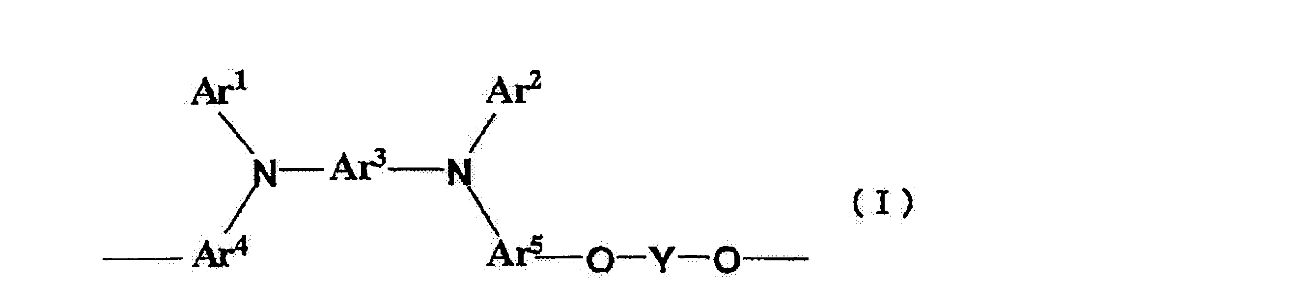
(式(I)中、Ar1及びAr2は、それぞれ独立して、置換基を有していてもよい芳香族炭化水素基又は置換基を有していてもよい芳香族複素環基を表す。Ar3~Ar5は、それぞれ独立して、置換基を有していてもよい芳香族炭化水素基又は置換基を有していてもよい芳香族複素環基を表す。Yは、下記の連結基群の中から選ばれる連結基を表す。また、Ar1~Ar5のうち、同一のN原子に結合する二つの基は互いに結合して環を形成してもよい。
(In formula (I), Ar 1 and Ar 2 each independently represent an aromatic hydrocarbon group which may have a substituent or an aromatic heterocyclic group which may have a substituent. Ar 3 to Ar 5 each independently represents an aromatic hydrocarbon group which may have a substituent or an aromatic heterocyclic group which may have a substituent. Represents a linking group selected from the group of linking groups, and two groups of Ar 1 to Ar 5 that are bonded to the same N atom may be bonded to each other to form a ring.

(上記各式中、Ar6~Ar16は、それぞれ独立して、置換基を有していてもよい芳香族炭化水素基又は置換基を有していてもよい芳香族複素環基を表す。R5及びR6は、それぞれ独立して、水素原子又は任意の置換基を表す。)
(In the above formulas, Ar 6 to Ar 16 each independently represents an aromatic hydrocarbon group which may have a substituent or an aromatic heterocyclic group which may have a substituent. R 5 and R 6 each independently represents a hydrogen atom or an arbitrary substituent.)
Ar1~Ar16の芳香族炭化水素基及び芳香族複素環基としては、高分子化合物の溶解性、耐熱性、正孔注入・輸送性の点から、ベンゼン環、ナフタレン環、フェナントレン環、チオフェン環、ピリジン環由来の基が好ましく、ベンゼン環、ナフタレン環由来の基がさらに好ましい。
Ar1~Ar16の芳香族炭化水素基及び芳香族複素環基は、さらに置換基を有していてもよい。置換基の分子量としては、通常400以下、中でも250以下程度が好ましい。置換基としては、アルキル基、アルケニル基、アルコキシ基、芳香族炭化水素基、芳香族複素環基などが好ましい。
R5及びR6が任意の置換基である場合、該置換基としては、アルキル基、アルケニル基、アルコキシ基、シリル基、シロキシ基、芳香族炭化水素基、芳香族複素環基などが挙げられる。 The aromatic hydrocarbon group and aromatic heterocyclic group of Ar 1 to Ar 16 include a benzene ring, a naphthalene ring, a phenanthrene ring, and a thiophene from the viewpoint of the solubility, heat resistance, and hole injection / transport properties of the polymer compound. A group derived from a ring or a pyridine ring is preferred, and a group derived from a benzene ring or a naphthalene ring is more preferred.
The aromatic hydrocarbon group and aromatic heterocyclic group of Ar 1 to Ar 16 may further have a substituent. The molecular weight of the substituent is usually 400 or less, preferably about 250 or less. As the substituent, an alkyl group, an alkenyl group, an alkoxy group, an aromatic hydrocarbon group, an aromatic heterocyclic group and the like are preferable.
When R 5 and R 6 are optional substituents, examples of the substituent include alkyl groups, alkenyl groups, alkoxy groups, silyl groups, siloxy groups, aromatic hydrocarbon groups, aromatic heterocyclic groups, and the like. .
式(I)で表される繰り返し単位を有する芳香族三級アミン高分子化合物の具体例としては、国際公開第2005/089024号に記載のものが挙げられる。また、正孔輸送性化合物としては、ポリチオフェンの誘導体である3,4-ethylenedioxythiophene(3,4-エチレンジオキシチオフェン)を高分子量ポリスチレンスルホン酸中で重合してなる導電性ポリマー(PEDOT/PSS)もまた好ましい。また、このポリマーの末端をメタクリレート等でキャップしたものであってもよい。
Specific examples of the aromatic tertiary amine polymer compound having a repeating unit represented by the formula (I) include those described in International Publication No. 2005/089024. In addition, as a hole transporting compound, a conductive polymer (PEDOT / PSS) obtained by polymerizing 3,4-ethylenedioxythiophene (3,4-ethylenedioxythiophene), a polythiophene derivative, in high molecular weight polystyrene sulfonic acid. Is also preferred. Moreover, the end of this polymer may be capped with methacrylate or the like.
正孔注入層形成用組成物中の、正孔輸送性化合物の濃度は本発明の効果を著しく損なわない限り任意であるが、膜厚の均一性の点で通常0.01重量%以上、好ましくは0.1重量%以上、さらに好ましくは0.5重量%以上、また、通常70重量%以下、好ましくは60重量%以下、さらに好ましくは50重量%以下である。この濃度が大きすぎると膜厚ムラが生じる可能性があり、また、小さすぎると成膜された正孔注入層に欠陥が生じる可能性がある。
The concentration of the hole transporting compound in the composition for forming a hole injection layer is arbitrary as long as the effect of the present invention is not significantly impaired, but is usually 0.01% by weight or more, preferably in terms of film thickness uniformity. Is 0.1% by weight or more, more preferably 0.5% by weight or more, and usually 70% by weight or less, preferably 60% by weight or less, more preferably 50% by weight or less. If this concentration is too high, film thickness unevenness may occur, and if it is too low, defects may occur in the formed hole injection layer.
(電子受容性化合物)
正孔注入層は電子受容性化合物を含有することが好ましく、したがって正孔注入層用組成物も電子受容性化合物を含有していることが好ましい。電子受容性化合物としては、酸化力を有し、上述の正孔輸送性化合物から一電子を受容する能力を有する化合物が好ましい。具体的には、電子親和力が4eV以上である化合物が好ましく、5eV以上の化合物がさらに好ましい。 (Electron-accepting compound)
The hole injection layer preferably contains an electron-accepting compound, and therefore the hole-injection layer composition preferably also contains an electron-accepting compound. As the electron-accepting compound, a compound having an oxidizing power and an ability to accept one electron from the above-described hole-transporting compound is preferable. Specifically, a compound having an electron affinity of 4 eV or more is preferable, and a compound of 5 eV or more is more preferable.
電子受容性化合物としては、例えば、トリアリールホウ素化合物、ハロゲン化金属、ルイス酸、有機酸、オニウム塩、アリールアミンとハロゲン化金属との塩、及び、アリールアミンとルイス酸との塩よりなる群から選ばれる1種又は2種以上の化合物等が挙げられる。さらに具体的には、4-イソプロピル-4’-メチルジフェニルヨードニウムテトラキス(ペンダフルオロフェニル)ボラート、トリフェニルスルホニウムテトラフルオロボラート等の有機基の置換したオニウム塩(国際公開第2005/089024号);塩化鉄(III)(日本国特開平11-251067号公報)、ペルオキソ二硫酸アンモニウム等の高原子価の無機化合物;テトラシアノエチレン等のシアノ化合物、トリス(ペンダフルオロフェニル)ボラン(日本国特開2003-31365号公報)等の芳香族ホウ素化合物;フラーレン誘導体;ヨウ素等が挙げられる。なお、電子受容性化合物は、1種類のみを用いてもよく、2種類以上を任意の組み合わせ及び任意の比率で併用してもよい。
Examples of the electron-accepting compound include a triaryl boron compound, a metal halide, a Lewis acid, an organic acid, an onium salt, a salt of an arylamine and a metal halide, and a salt of an arylamine and a Lewis acid. 1 type, or 2 or more types of compounds etc. chosen from are mentioned. More specifically, an onium salt substituted with an organic group such as 4-isopropyl-4′-methyldiphenyliodonium tetrakis (pentafluorophenyl) borate and triphenylsulfonium tetrafluoroborate (WO 2005/089024); High-valent inorganic compounds such as iron (III) chloride (Japanese Patent Laid-Open No. 11-251067), ammonium peroxodisulfate; cyano compounds such as tetracyanoethylene, tris (pendafluorophenyl) borane (Japanese Patent Laid-Open No. 2003) Aromatic boron compounds; fullerene derivatives; iodine and the like. In addition, only 1 type may be used for an electron-accepting compound, and 2 or more types may be used together by arbitrary combinations and arbitrary ratios.
これらの電子受容性化合物は、正孔輸送性化合物を酸化するため、正孔注入層の導電率を向上させることができる。
電子受容性化合物の正孔輸送性化合物に対する含有量は、通常0.1モル%以上、好ましくは1モル%以上である。但し、通常100モル%以下、好ましくは40モル%以下である。 Since these electron accepting compounds oxidize the hole transporting compound, the conductivity of the hole injection layer can be improved.
The content of the electron-accepting compound with respect to the hole-transporting compound is usually 0.1 mol% or more, preferably 1 mol% or more. However, it is usually 100 mol% or less, preferably 40 mol% or less.
(溶媒)
正孔注入層用組成物が含有する溶媒のうち少なくとも1種は、正孔注入層の材料を溶解しうる溶媒であることが好ましい。
また、溶媒の沸点は、通常110℃以上、好ましくは140℃以上、より好ましくは200℃以上であり、通常400℃以下、好ましくは300℃以下である。溶媒の沸点が低すぎると形成した膜の乾燥速度が速く、膜質が悪化する可能性がある。また、溶媒の沸点が高すぎると乾燥工程の温度が高くなり、他の層や基板1(例えば、ガラス基板)に悪影響を与える可能性がある。 (solvent)
At least one of the solvents contained in the hole injection layer composition is preferably a solvent that can dissolve the material of the hole injection layer.
Moreover, the boiling point of a solvent is 110 degreeC or more normally, Preferably it is 140 degreeC or more, More preferably, it is 200 degreeC or more, and is 400 degrees C or less normally, Preferably it is 300 degrees C or less. If the boiling point of the solvent is too low, the drying speed of the formed film is high, and the film quality may deteriorate. Moreover, if the boiling point of the solvent is too high, the temperature of the drying process increases, which may adversely affect other layers and the substrate 1 (for example, a glass substrate).
溶媒の例を挙げると、エーテル系溶媒、エステル系溶媒、芳香族炭化水素系溶媒、アミド系溶媒などが挙げられる。具体的に、エーテル系溶媒としては、例えば、エチレングリコールジメチルエーテル、エチレングリコールジエチルエーテル、プロピレングリコール-1-モノメチルエーテルアセタート(PGMEA)等の脂肪族エーテル;1,2-ジメトキシベンゼン、1,3-ジメトキシベンゼン、アニソール、フェネトール、2-メトキシトルエン、3-メトキシトルエン、4-メトキシトルエン、2,3-ジメチルアニソール、2,4-ジメチルアニソール等の芳香族エーテル、等が挙げられる。また、エステル系溶媒としては、例えば、酢酸フェニル、プロピオン酸フェニル、安息香酸メチル、安息香酸エチル、安息香酸プロピル、安息香酸n-ブチル等の芳香族エステル、等が挙げられる。さらに、芳香族炭化水素系溶媒としては、例えば、トルエン、キシレン、シクロヘキシルベンゼン、3-イロプロピルビフェニル、1,2,3,4-テトラメチルベンゼン、1,4-ジイソプロピルベンゼン、シクロヘキシルベンゼン、メチルナフタレン等が挙げられる。また、アミド系溶媒としては、例えば、N,N-ジメチルホルムアミド、N,N-ジメチルアセトアミド、等が挙げられる。またその他、ジメチルスルホキシド、等も溶媒として用いることができる。
Examples of solvents include ether solvents, ester solvents, aromatic hydrocarbon solvents, amide solvents, and the like. Specifically, examples of the ether solvent include aliphatic ethers such as ethylene glycol dimethyl ether, ethylene glycol diethyl ether, propylene glycol-1-monomethyl ether acetate (PGMEA); 1,2-dimethoxybenzene, 1,3- And aromatic ethers such as dimethoxybenzene, anisole, phenetole, 2-methoxytoluene, 3-methoxytoluene, 4-methoxytoluene, 2,3-dimethylanisole, and 2,4-dimethylanisole. Examples of the ester solvent include aromatic esters such as phenyl acetate, phenyl propionate, methyl benzoate, ethyl benzoate, propyl benzoate, and n-butyl benzoate. Further, examples of the aromatic hydrocarbon solvent include toluene, xylene, cyclohexylbenzene, 3-isopropylpropylphenyl, 1,2,3,4-tetramethylbenzene, 1,4-diisopropylbenzene, cyclohexylbenzene, and methylnaphthalene. Etc. Examples of the amide solvent include N, N-dimethylformamide, N, N-dimethylacetamide, and the like. In addition, dimethyl sulfoxide and the like can also be used as a solvent.
上述した溶媒の中でも、正孔注入層の材料を溶解する能力(溶解能)、若しくは材料との親和性が高い溶媒の方が好ましい。正孔注入層用組成物の濃度を任意に設定して、成膜工程の効率に優れる濃度の組成物を調製できるためである。
なお、溶媒は1種類を用いてもよく、2種類以上を任意の組み合わせ及び任意の比率で併用してもよい。 Among the solvents described above, a solvent having a high ability to dissolve the material of the hole injection layer (dissolving ability) or a high affinity with the material is preferable. This is because a composition having a concentration excellent in the efficiency of the film forming process can be prepared by arbitrarily setting the concentration of the composition for the hole injection layer.
In addition, 1 type may be used for a solvent and it may use 2 or more types together by arbitrary combinations and arbitrary ratios.
(その他の成分)
正孔注入層の材料としては、本発明の効果を著しく損なわない限り、正孔輸送性化合物及び電子受容性化合物以外に、さらにその他の成分を含有させてもよい。その他の成分の例としては、各種の発光材料、電子輸送性化合物、バインダー樹脂、塗布性改良剤などが挙げられる。なお、その他の成分は、1種類を用いてもよく、2種類以上を任意の組み合わせ及び任意の比率で併用してもよい。 (Other ingredients)
As a material for the hole injection layer, other components may be further contained in addition to the hole transporting compound and the electron accepting compound as long as the effects of the present invention are not significantly impaired. Examples of other components include various light emitting materials, electron transporting compounds, binder resins, and coating property improving agents. In addition, 1 type may be used for another component and it may use 2 or more types together by arbitrary combinations and arbitrary ratios.
(成膜方法)
正孔注入層用組成物を調製後、この組成物を湿式成膜法により、正孔注入層の下層に該当する層(通常は、陽極)上に塗布し、乾燥することによって正孔注入層を形成する。塗布後、通常は加熱等により乾燥を行う。加熱工程において使用する加熱手段は、本発明の効果を著しく損なわない限り限定されない。加熱手段の例を挙げると、クリーンオーブン、ホットプレート、赤外線、ハロゲンヒーター、マイクロ波照射などが挙げられる。中でも、膜全体に均等に熱を与えるためには、クリーンオーブン及びホットプレートが好ましい。ただし、正孔注入層用組成物が本発明のアリールアミンポリマーを含有する場合には、塗布後に架橋を行わせるようにする。 (Film formation method)
After preparing the composition for the hole injection layer, the composition is applied onto a layer (usually an anode) corresponding to the lower layer of the hole injection layer by a wet film forming method, and dried to form the hole injection layer. Form. After application, usually drying is performed by heating or the like. The heating means used in the heating step is not limited as long as the effects of the present invention are not significantly impaired. Examples of the heating means include a clean oven, a hot plate, infrared rays, a halogen heater, and microwave irradiation. Among them, a clean oven and a hot plate are preferable in order to uniformly apply heat to the entire film. However, when the composition for hole injection layers contains the arylamine polymer of the present invention, crosslinking is performed after coating.
なお、真空蒸着法による層形成の場合には、まず材料(正孔輸送性化合物、電子受容性化合物等)の1種又は2種以上を真空容器内に設置されたるつぼに入れ(2種以上材料を用いる場合は各々のるつぼに入れ)、真空容器内を適当な真空ポンプで10-4Pa程度まで排気する。その後、るつぼを加熱して(2種以上材料を用いる場合は各々のるつぼを加熱して)、蒸発量を制御して蒸発させ(2種以上材料を用いる場合は各々独立に蒸発量を制御して蒸発させ)、るつぼと向き合って置かれた基板の陽極上に正孔注入層を形成させる。なお、2種以上の材料を用いる場合は、それらの混合物をるつぼに入れ、加熱し蒸発させて正孔注入層の形成に用いることもできる。
In the case of forming a layer by a vacuum deposition method, first, one or more materials (hole transporting compound, electron accepting compound, etc.) are put in a crucible installed in a vacuum vessel (two or more types). When using the material, put it in each crucible) and evacuate the inside of the vacuum vessel to about 10 −4 Pa with an appropriate vacuum pump. Then, the crucible is heated (each crucible is heated when two or more materials are used), and the evaporation amount is controlled to evaporate (when two or more materials are used, the evaporation amount is controlled independently). And a hole injection layer is formed on the anode of the substrate placed facing the crucible. In addition, when using 2 or more types of materials, they can also be put into a crucible, can be heated and evaporated, and can be used for formation of a positive hole injection layer.
正孔注入層の膜厚は、通常5nm以上、好ましくは10nm以上、また、通常1000nm以下、好ましくは500nm以下の範囲である。膜厚が薄すぎると正孔注入能が不十分になる可能性があり、厚すぎると抵抗が高くなる可能性がある。
なお、正孔注入層は単一の層からなる構成としてもよいが、複数の層が積層された構成としてもよい。後者の場合、複数の層は同一の材料からなる層であってもよいし、異なる材料からなる層であってもよい。 The thickness of the hole injection layer is usually 5 nm or more, preferably 10 nm or more, and usually 1000 nm or less, preferably 500 nm or less. If the film thickness is too thin, the hole injection ability may be insufficient, and if it is too thick, the resistance may be increased.
In addition, although a positive hole injection layer is good also as a structure which consists of a single layer, it is good also as a structure by which the several layer was laminated | stacked. In the latter case, the plurality of layers may be layers made of the same material or layers made of different materials.
[正孔輸送層]
本発明に係る正孔輸送層の形成方法は真空蒸着法でも、湿式成膜法でもよく、特に制限はないが、ダークスポット低減の観点から正孔輸送層を湿式成膜法により形成することが好ましい。
正孔輸送層は、正孔注入層がある場合には正孔注入層の上に、正孔注入層が無い場合には陽極の上に形成することができる。また、本発明の有機電界発光素子は、正孔輸送層を省いた構成であってもよい。
正孔輸送層を形成する材料としては、正孔輸送性が高く、かつ、注入された正孔を効率よく輸送することができる材料であることが好ましい。そのために、イオン化ポテンシャルが小さく、可視光の光に対して透明性が高く、正孔移動度が大きく、安定性に優れ、トラップとなる不純物が製造時や使用時に発生しにくいことが好ましい。また、多くの場合、発光層に接するため、発光層からの発光を消光したり、発光層との間でエキサイプレックスを形成して効率を低下させたりしないことが好ましい。 [Hole transport layer]
The formation method of the hole transport layer according to the present invention may be a vacuum deposition method or a wet film formation method, and is not particularly limited, but the hole transport layer may be formed by a wet film formation method from the viewpoint of reducing dark spots. preferable.
The hole transport layer can be formed on the hole injection layer when there is a hole injection layer and on the anode when there is no hole injection layer. The organic electroluminescent device of the present invention may have a configuration in which the hole transport layer is omitted.
The material for forming the hole transport layer is preferably a material having high hole transportability and capable of efficiently transporting injected holes. Therefore, it is preferable that the ionization potential is small, the transparency to visible light is high, the hole mobility is large, the stability is high, and impurities that become traps are not easily generated during manufacturing or use. In many cases, since it is in contact with the light emitting layer, it is preferable not to quench the light emitted from the light emitting layer or reduce the efficiency by forming an exciplex with the light emitting layer.
このような正孔輸送層の材料としては、従来、正孔輸送層の構成材料として用いられている材料であればよく、例えば、前述の正孔注入層に使用される正孔輸送性化合物として例示したものが挙げられる。また、アリールアミン誘導体、フルオレン誘導体、スピロ誘導体、カルバゾール誘導体、ピリジン誘導体、ピラジン誘導体、ピリミジン誘導体、トリアジン誘導体、キノリン誘導体、フェナントロリン誘導体、フタロシアニン誘導体、ポルフィリン誘導体、シロール誘導体、オリゴチオフェン誘導体、縮合多環芳香族誘導体、金属錯体などが挙げられる。
As a material of such a hole transport layer, any material that has been conventionally used as a constituent material of a hole transport layer may be used. For example, as a hole transport compound used in the above-described hole injection layer What was illustrated is mentioned. In addition, arylamine derivatives, fluorene derivatives, spiro derivatives, carbazole derivatives, pyridine derivatives, pyrazine derivatives, pyrimidine derivatives, triazine derivatives, quinoline derivatives, phenanthroline derivatives, phthalocyanine derivatives, porphyrin derivatives, silole derivatives, oligothiophene derivatives, condensed polycyclic aromatics Group derivatives, metal complexes and the like.
また、例えば、ポリビニルカルバゾール誘導体、ポリアリールアミン誘導体、ポリビニルトリフェニルアミン誘導体、ポリフルオレン誘導体、ポリアリーレン誘導体、テトラフェニルベンジジンを含有するポリアリーレンエーテルサルホン誘導体、ポリアリーレンビニレン誘導体、ポリシロキサン誘導体、ポリチオフェン誘導体、ポリ(p-フェニレンビニレン)誘導体等が挙げられる。これらは、交互共重合体、ランダム重合体、ブロック重合体又はグラフト共重合体のいずれであってもよい。また、主鎖に枝分かれがあり末端部が3つ以上ある高分子や、所謂デンドリマーであってもよい。
In addition, for example, polyvinylcarbazole derivatives, polyarylamine derivatives, polyvinyltriphenylamine derivatives, polyfluorene derivatives, polyarylene derivatives, polyarylene ether sulfone derivatives containing tetraphenylbenzidine, polyarylene vinylene derivatives, polysiloxane derivatives, polythiophenes Derivatives, poly (p-phenylene vinylene) derivatives, and the like. These may be any of an alternating copolymer, a random polymer, a block polymer, or a graft copolymer. Further, it may be a polymer having a branched main chain and three or more terminal portions, or a so-called dendrimer.
中でも、ポリアリールアミン誘導体やポリアリーレン誘導体が好ましい。
ポリアリールアミン誘導体としては、下記式(II)で表される繰り返し単位を含む重合体であることが好ましい。特に、下記式(II)で表される繰り返し単位からなる重合体であることが好ましく、この場合、繰り返し単位それぞれにおいて、Ara又はArbが異なっているものであってもよい。 Of these, polyarylamine derivatives and polyarylene derivatives are preferred.
The polyarylamine derivative is preferably a polymer containing a repeating unit represented by the following formula (II). In particular, the polymer is preferably composed of a repeating unit represented by the following formula (II). In this case, Ar a or Ar b may be different in each repeating unit.

(式(II)中、Ara及びArbは、それぞれ独立して、置換基を有していてもよい、芳香族炭化水素基又は芳香族複素環基を表す。)
(In formula (II), Ar a and Ar b each independently represent an aromatic hydrocarbon group or an aromatic heterocyclic group which may have a substituent.)
置換基を有していてもよい芳香族炭化水素基としては、例えば、ベンゼン環、ナフタレン環、アントラセン環、フェナントレン環、ペリレン環、テトラセン環、ピレン環、ベンズピレン環、クリセン環、トリフェニレン環、アセナフテン環、フルオランテン環、フルオレン環などの、6員環の単環又は2~5縮合環由来の基及びこれらの環が2環以上直接結合で連結してなる基が挙げられる。
Examples of the aromatic hydrocarbon group which may have a substituent include, for example, a benzene ring, naphthalene ring, anthracene ring, phenanthrene ring, perylene ring, tetracene ring, pyrene ring, benzpyrene ring, chrysene ring, triphenylene ring, and acenaphthene. Examples thereof include a group derived from a 6-membered monocyclic ring or a 2-5 condensed ring, such as a ring, a fluoranthene ring, a fluorene ring, and a group in which these rings are linked by a direct bond.
置換基を有していてもよい芳香族複素環基としては、例えばフラン環、ベンゾフラン環、チオフェン環、ベンゾチオフェン環、ピロール環、ピラゾール環、イミダゾール環、オキサジアゾール環、インドール環、カルバゾール環、ピロロイミダゾール環、ピロロピラゾール環、ピロロピロール環、チエノピロール環、チエノチオフェン環、フロピロール環、フロフラン環、チエノフラン環、ベンゾイソオキサゾール環、ベンゾイソチアゾール環、ベンゾイミダゾール環、ピリジン環、ピラジン環、ピリダジン環、ピリミジン環、トリアジン環、キノリン環、イソキノリン環、シノリン環、キノキサリン環、フェナントリジン環、ベンゾイミダゾール環、ペリミジン環、キナゾリン環、キナゾリノン環、アズレン環などの、5又は6員環の単環又は2~4縮合環由来の基及びこれらの環が2環以上直接結合で連結してなる基が挙げられる。
Examples of the aromatic heterocyclic group which may have a substituent include a furan ring, a benzofuran ring, a thiophene ring, a benzothiophene ring, a pyrrole ring, a pyrazole ring, an imidazole ring, an oxadiazole ring, an indole ring, and a carbazole ring. , Pyrroloimidazole ring, pyrrolopyrazole ring, pyrrolopyrrole ring, thienopyrrole ring, thienothiophene ring, furopyrrole ring, furofuran ring, thienofuran ring, benzoisoxazole ring, benzoisothiazole ring, benzimidazole ring, pyridine ring, pyrazine ring, pyridazine Ring, pyrimidine ring, triazine ring, quinoline ring, isoquinoline ring, sinoline ring, quinoxaline ring, phenanthridine ring, benzimidazole ring, perimidine ring, quinazoline ring, quinazolinone ring, azulene ring, etc. Or 2-4 fused ring group derived from and these rings include a group formed by connecting a direct bond or two or more rings.
溶解性、耐熱性の点から、Ara及びArbは、各々独立に、ベンゼン環、ナフタレン環、アントラセン環、フェナントレン環、トリフェニレン環、ピレン環、チオフェン環、ピリジン環、フルオレン環からなる群より選ばれる環由来の基やベンゼン環が2環以上連結してなる基(例えば、ビフェニル基やターフェニル基)が好ましい。
中でも、ベンゼン環由来の基(フェニル基)、ベンゼン環が2環連結してなる基(ビフェニル基)及びフルオレン環由来の基(フルオレニル基)が好ましい。 In view of solubility and heat resistance, Ar a and Ar b are each independently selected from the group consisting of a benzene ring, naphthalene ring, anthracene ring, phenanthrene ring, triphenylene ring, pyrene ring, thiophene ring, pyridine ring, and fluorene ring. A group derived from a selected ring or a group formed by linking two or more benzene rings (for example, a biphenyl group or a terphenyl group) is preferable.
Among these, a group derived from a benzene ring (phenyl group), a group formed by connecting two benzene rings (biphenyl group), and a group derived from a fluorene ring (fluorenyl group) are preferable.
Ara及びArbにおける芳香族炭化水素基及び芳香族複素環基が有していてもよい置換基としては、アルキル基、アルケニル基、アルキニル基、アルコキシ基、アリールオキシ基、アルコキシカルボニル基、ジアルキルアミノ基、ジアリールアミノ基、アシル基、ハロゲン原子、ハロアルキル基、アルキルチオ基、アリールチオ基、シリル基、シロキシ基、シアノ基、芳香族炭化水素環基、芳香族複素環基などが挙げられる。
Examples of the substituent that the aromatic hydrocarbon group and aromatic heterocyclic group in Ar a and Ar b may have include an alkyl group, an alkenyl group, an alkynyl group, an alkoxy group, an aryloxy group, an alkoxycarbonyl group, and a dialkyl. Examples thereof include an amino group, a diarylamino group, an acyl group, a halogen atom, a haloalkyl group, an alkylthio group, an arylthio group, a silyl group, a siloxy group, a cyano group, an aromatic hydrocarbon ring group, and an aromatic heterocyclic group.
ポリアリーレン誘導体としては、前記式(II)におけるAraやArbとして例示した置換基を有していてもよい、芳香族炭化水素基又は芳香族複素環基などのアリーレン基をその繰り返し単位に有する重合体が挙げられる。
ポリアリーレン誘導体としては、下記式(III-1)及び/又は下記式(III-2)からなる繰り返し単位を有する重合体が好ましい。 As the polyarylene derivative, an arylene group such as an aromatic hydrocarbon group or an aromatic heterocyclic group which may have a substituent exemplified as Ar a or Ar b in the formula (II) is used as a repeating unit. The polymer which has is mentioned.
As the polyarylene derivative, a polymer having a repeating unit represented by the following formula (III-1) and / or the following formula (III-2) is preferable.

(式(III-1)中、Ra、Rb、Rc及びRdは、それぞれ独立に、アルキル基、アルコキシ基、フェニルアルキル基、フェニルアルコキシ基、フェニル基、フェノキシ基、アルキルフェニル基、アルコキシフェニル基、アルキルカルボニル基、アルコキシカルボニル基、又はカルボキシ基を表す。t及びsは、それぞれ独立に、0~3の整数を表す。t又はsが2以上の場合、一分子中に含まれる複数のRa又はRbは同一であっても異なっていてもよく、隣接するRa又はRb同士で環を形成していてもよい。)
(In the formula (III-1), R a , R b , R c and R d are each independently an alkyl group, an alkoxy group, a phenylalkyl group, a phenylalkoxy group, a phenyl group, a phenoxy group, an alkylphenyl group, Represents an alkoxyphenyl group, an alkylcarbonyl group, an alkoxycarbonyl group, or a carboxy group, and t and s each independently represent an integer of 0 to 3. When t or s is 2 or more, they are contained in one molecule. A plurality of R a or R b may be the same or different, and adjacent R a or R b may form a ring.)

(式(III-2)中、Re及びRfは、それぞれ独立に、上記式(III-1)におけるRa、Rb、Rc又はRdと同義である。r及びuは、それぞれ独立に、0~3の整数を表す。r又はuが2以上の場合、一分子中に含まれる複数のRe及びRfは同一であっても異なっていてもよく、隣接するRe又はRf同士で環を形成していてもよい。Xは、5員環又は6員環を構成する原子又は原子群を表す。)
Xの具体例としては、―O―、―BR―、―NR―、―SiR2―、―PR―、―SR―、―CR2―又はこれらが結合してなる基である。尚、Rは、水素原子又は任意の有機基を表す。本発明における有機基とは、少なくとも一つの炭素原子を含む基である。 (In the formula (III-2), R e and R f are each independently the same as R a , R b , R c or R d in the formula (III-1). Independently represents an integer of 0 to 3. When r or u is 2 or more, a plurality of R e and R f contained in one molecule may be the same or different, and adjacent R e or R f may form a ring, and X represents an atom or a group of atoms constituting a 5-membered ring or a 6-membered ring.)
Examples of X, -O -, - BR - , - NR -, - SiR 2 -, - PR -, - SR -, - it is or they are formed by bonding group - CR 2. R represents a hydrogen atom or an arbitrary organic group. The organic group in the present invention is a group containing at least one carbon atom.
また、ポリアリーレン誘導体としては、上記式(III-1)及び/又は上記式(III-2)からなる繰り返し単位に加えて、さらに下記式(III-3)で表される繰り返し単位を有することが好ましい。
Further, the polyarylene derivative has a repeating unit represented by the following formula (III-3) in addition to the repeating unit represented by the above formula (III-1) and / or the above formula (III-2). Is preferred.

(式(III-3)中、Arc~Arjは、それぞれ独立に、置換基を有していてもよい、芳香族炭化水素基又は芳香族複素環基を表す。v及びwは、それぞれ独立に0又は1を表す。)
Arc~Arjの具体例としては、前記式(II)における、Ara及びArbと同様である。
上記式(III-1)~(III-3)の具体例及びポリアリーレン誘導体の具体例等は、日本国特開2008-98619号公報に記載のものなどが挙げられる。 (In the formula (III-3), Ar c to Ar j each independently represents an aromatic hydrocarbon group or an aromatic heterocyclic group which may have a substituent. Independently represents 0 or 1.)
Specific examples of Ar c to Ar j are the same as Ar a and Ar b in the formula (II).
Specific examples of the above formulas (III-1) to (III-3) and specific examples of polyarylene derivatives include those described in Japanese Patent Application Laid-Open No. 2008-98619.
湿式成膜法で正孔輸送層を形成する場合は、上記正孔注入層の形成と同様にして、正孔輸送層形成用組成物を調製した後、湿式成膜後、加熱乾燥させる。
正孔輸送層形成用組成物には、上述の正孔輸送性化合物の他、溶媒を含有する。用いる溶媒は上記正孔注入層形成用組成物に用いたものと同様である。また、成膜条件、加熱乾燥条件等も正孔注入層の形成の場合と同様である。 When the hole transport layer is formed by a wet film formation method, a composition for forming a hole transport layer is prepared in the same manner as the formation of the hole injection layer, followed by heat drying after the wet film formation.
The composition for forming a hole transport layer contains a solvent in addition to the above hole transport compound. The solvent used is the same as that used for the composition for forming a hole injection layer. The film forming conditions, heat drying conditions, and the like are the same as in the case of forming the hole injection layer.
真空蒸着法により正孔輸送層を形成する場合もまた、その成膜条件等は上記正孔注入層の形成の場合と同様である。
正孔輸送層は、上記正孔輸送性化合物の他、各種の発光材料、電子輸送性化合物、バインダー樹脂、塗布性改良剤などを含有していてもよい。
正孔輸送層はまた、架橋性化合物を架橋して形成される層であってもよい。架橋性化合物は、架橋性基を有する化合物であって、架橋することにより網目状高分子化合物を形成する。 In the case where the hole transport layer is formed by the vacuum deposition method, the film forming conditions are the same as those in the case of forming the hole injection layer.
The hole transport layer may contain various light emitting materials, electron transport compounds, binder resins, coatability improvers, and the like in addition to the hole transport compound.
The hole transport layer may also be a layer formed by crosslinking a crosslinkable compound. The crosslinkable compound is a compound having a crosslinkable group, and forms a network polymer compound by crosslinking.
この架橋性基の例を挙げると、オキセタン、エポキシなどの環状エーテル由来の基;ビニル基、トリフルオロビニル基、スチリル基、アクリル基、メタクリロイル、シンナモイル等の不飽和二重結合由来の基;ベンゾシクロブテン由来の基などが挙げられる。
架橋性化合物は、モノマー、オリゴマー、ポリマーのいずれであってもよい。 架橋性化合物は1種のみを有していてもよく、2種以上を任意の組み合わせ及び比率で有していてもよい。 Examples of this crosslinkable group include groups derived from cyclic ethers such as oxetane and epoxy; groups derived from unsaturated double bonds such as vinyl, trifluorovinyl, styryl, acrylic, methacryloyl and cinnamoyl; benzo Examples include groups derived from cyclobutene.
The crosslinkable compound may be any of a monomer, an oligomer, and a polymer. The crosslinkable compound may have only 1 type, and may have 2 or more types by arbitrary combinations and ratios.
架橋性化合物としては、架橋性基を有する正孔輸送性化合物を用いることが好ましい。正孔輸送性化合物としては、上記の例示したものが挙げられ、これら正孔輸送性化合物に対して、架橋性基が主鎖又は側鎖に結合しているものが挙げられる。特に架橋性基は、アルキレン基等の連結基を介して、主鎖に結合していることが好ましい。また、特に正孔輸送性化合物としては、架橋性基を有する繰り返し単位を含む重合体であることが好ましく、上記式(II)や式(III-1)~(III-3)に架橋性基が直接又は連結基を介して結合した繰り返し単位を有する重合体であることが好ましい。
As the crosslinkable compound, it is preferable to use a hole transporting compound having a crosslinkable group. Examples of the hole transporting compound include those exemplified above, and those having a crosslinkable group bonded to the main chain or side chain with respect to these hole transporting compounds. In particular, the crosslinkable group is preferably bonded to the main chain via a linking group such as an alkylene group. In particular, the hole transporting compound is preferably a polymer containing a repeating unit having a crosslinkable group, and the above formula (II) and formulas (III-1) to (III-3) can be used as a crosslinkable group. Is preferably a polymer having a repeating unit bonded directly or via a linking group.
架橋性化合物としては、架橋性基を有する正孔輸送性化合物を用いることが好ましい。正孔輸送性化合物の例を挙げると、ピリジン誘導体、ピラジン誘導体、ピリミジン誘導体、トリアジン誘導体、キノリン誘導体、フェナントロリン誘導体、カルバゾール誘導体、フタロシアニン誘導体、ポルフィリン誘導体等の含窒素芳香族化合物誘導体;トリフェニルアミン誘導体;シロール誘導体;オリゴチオフェン誘導体、縮合多環芳香族誘導体、金属錯体などが挙げられる。その中でも、ピリジン誘導体、ピラジン誘導体、ピリミジン誘導体、トリアジン誘導体、キノリン誘導体、フェナントロリン誘導体、カルバゾール誘導体等の含窒素芳香族誘導体;トリフェニルアミン誘導体、シロール誘導体、縮合多環芳香族誘導体、金属錯体などが好ましく、特に、トリフェニルアミン誘導体がより好ましい。
As the crosslinkable compound, it is preferable to use a hole transporting compound having a crosslinkable group. Examples of hole transporting compounds include nitrogen-containing aromatic compound derivatives such as pyridine derivatives, pyrazine derivatives, pyrimidine derivatives, triazine derivatives, quinoline derivatives, phenanthroline derivatives, carbazole derivatives, phthalocyanine derivatives, porphyrin derivatives; triphenylamine derivatives Silole derivatives; oligothiophene derivatives, condensed polycyclic aromatic derivatives, metal complexes and the like. Among them, nitrogen-containing aromatic derivatives such as pyridine derivatives, pyrazine derivatives, pyrimidine derivatives, triazine derivatives, quinoline derivatives, phenanthroline derivatives, carbazole derivatives; triphenylamine derivatives, silole derivatives, condensed polycyclic aromatic derivatives, metal complexes, etc. Particularly preferred are triphenylamine derivatives.
架橋性化合物を架橋して正孔輸送層を形成するには、通常、架橋性化合物を溶媒に溶解又は分散した正孔輸送層形成用組成物を調製して、湿式成膜により成膜して架橋させる。
正孔輸送層形成用組成物には、架橋性化合物の他、架橋反応を促進する添加物を含んでいてもよい。架橋反応を促進する添加物の例を挙げると、アルキルフェノン化合物、アシルホスフィンオキサイド化合物、メタロセン化合物、オキシムエステル化合物、アゾ化合物、オニウム塩等の重合開始剤及び重合促進剤;縮合多環炭化水素、ポルフィリン化合物、ジアリールケトン化合物等の光増感剤;などが挙げられる。 In order to form a hole transport layer by crosslinking a crosslinkable compound, a composition for forming a hole transport layer in which a crosslinkable compound is dissolved or dispersed in a solvent is usually prepared and formed by wet film formation. Crosslink.
The composition for forming a hole transport layer may contain an additive for promoting a crosslinking reaction in addition to the crosslinking compound. Examples of additives that accelerate the crosslinking reaction include polymerization initiators and polymerization accelerators such as alkylphenone compounds, acylphosphine oxide compounds, metallocene compounds, oxime ester compounds, azo compounds, onium salts; condensed polycyclic hydrocarbons, And photosensitizers such as porphyrin compounds and diaryl ketone compounds.
また、さらに、レベリング剤、消泡剤等の塗布性改良剤;電子受容性化合物;バインダー樹脂;などを含有していてもよい。
正孔輸送層形成用組成物は、架橋性化合物を通常0.01重量%以上、好ましくは0.05重量%以上、さらに好ましくは0.1重量%以上、通常50重量%以下、好ましくは20重量%以下、さらに好ましくは10重量%以下含有する。 Further, it may contain a coating property improving agent such as a leveling agent and an antifoaming agent; an electron accepting compound; a binder resin;
In the composition for forming a hole transport layer, the crosslinkable compound is usually 0.01% by weight or more, preferably 0.05% by weight or more, more preferably 0.1% by weight or more, usually 50% by weight or less, preferably 20%. It is contained by weight% or less, more preferably 10% by weight or less.
このような濃度で架橋性化合物を含む正孔輸送層形成用組成物を下層(通常は正孔注入層)上に成膜後、加熱及び/又は光などの電磁エネルギー照射により、架橋性化合物を架橋させて網目状高分子化合物を形成する。
成膜時の温度、湿度などの条件は、前記正孔注入層の湿式成膜時と同様である。
成膜後の加熱の手法は特に限定されない。加熱温度条件としては、通常120℃以上、好ましくは400℃以下である。 After forming a composition for forming a hole transport layer containing a crosslinkable compound at such a concentration on a lower layer (usually a hole injection layer), the crosslinkable compound is formed by heating and / or irradiation with electromagnetic energy such as light. A network polymer compound is formed by crosslinking.
Conditions such as temperature and humidity during film formation are the same as those during wet film formation of the hole injection layer.
The heating method after film formation is not particularly limited. As heating temperature conditions, it is 120 degreeC or more normally, Preferably it is 400 degrees C or less.
加熱時間としては、通常1分以上、好ましくは24時間以下である。加熱手段としては特に限定されないが、成膜された層を有する積層体をホットプレート上に載せたり、オーブン内で加熱するなどの手段が用いられる。例えば、ホットプレート上で120℃以上、1分間以上加熱する等の条件を用いることができる。
光などの電磁エネルギー照射による場合には、超高圧水銀ランプ、高圧水銀ランプ、ハロゲンランプ、赤外ランプ等の紫外・可視・赤外光源を直接用いて照射する方法、あるいは前述の光源を内蔵するマスクアライナ、コンベア型光照射装置を用いて照射する方法などが挙げられる。光以外の電磁エネルギー照射では、例えばマグネトロンにより発生させたマイクロ波を照射する装置、いわゆる電子レンジを用いて照射する方法が挙げられる。照射時間としては、膜の溶解性を低下させるために必要な条件を設定することが好ましいが、通常、0.1秒以上、好ましくは10時間以下照射される。 The heating time is usually 1 minute or longer, preferably 24 hours or shorter. The heating means is not particularly limited, and means such as placing a laminated body having a deposited layer on a hot plate or heating in an oven is used. For example, conditions such as heating on a hot plate at 120 ° C. or more for 1 minute or more can be used.
In the case of irradiation with electromagnetic energy such as light, a method of irradiating directly using an ultraviolet / visible / infrared light source such as an ultra-high pressure mercury lamp, a high-pressure mercury lamp, a halogen lamp or an infrared lamp, or the above-mentioned light source is incorporated. Examples include a mask aligner and a method of irradiation using a conveyor type light irradiation device. In electromagnetic energy irradiation other than light, for example, there is a method of irradiation using a device that irradiates a microwave generated by a magnetron, a so-called microwave oven. As the irradiation time, it is preferable to set conditions necessary for reducing the solubility of the film, but irradiation is usually performed for 0.1 seconds or longer, preferably 10 hours or shorter.
加熱及び光などの電磁エネルギー照射は、それぞれ単独、あるいは組み合わせて行ってもよい。組み合わせる場合、実施する順序は特に限定されない。
このようにして形成される正孔輸送層の膜厚は、通常5nm以上、好ましくは10nm以上であり、また通常300nm以下、好ましくは100nm以下である。 Irradiation of electromagnetic energy such as heating and light may be performed individually or in combination. When combined, the order of implementation is not particularly limited.
The film thickness of the hole transport layer thus formed is usually 5 nm or more, preferably 10 nm or more, and usually 300 nm or less, preferably 100 nm or less.
{バンク}
基板上、又は正孔輸送層上には、パターン状にバンクが設けられていてもよい。バンクのパターンの形状は特に限定されるものではなく、発光層6の形状や陰極の形状等に合わせて適宜選択されるが、網目状のパターン又はストライブ状のパターンであることが好ましい。
バンクにより区画された領域に設けられる層が、発光層である場合は、発光領域のパターンを反転させたパターン等とすることができる。陰極を区画すること等を目的として設けられる場合、上記バンクを陰極隔壁として利用し、有機電界発光パネルにおける、陰極のストライプ状パターニングに用いることができる。
またバンクの断面形状についても特に限定されず、例えば断面形状は矩形状であってもよく、半円形状であってもよく、また逆テーパー形状の台形状やテーパー形状の台形状等であってもよい。またバンクの上面から見た形状についても特に限定されず、矩形、楕円形、又は角が丸い長方形等の開口部をもつ形状、あるいは直線状の形状であってもよい。 {bank}
Banks may be provided in a pattern on the substrate or the hole transport layer. The shape of the bank pattern is not particularly limited and is appropriately selected according to the shape of thelight emitting layer 6, the shape of the cathode, and the like, but is preferably a mesh pattern or a stripe pattern.
When the layer provided in the region partitioned by the bank is a light emitting layer, a pattern obtained by inverting the pattern of the light emitting region can be used. When provided for the purpose of partitioning the cathode, etc., the bank can be used as a cathode partition, and can be used for striped patterning of the cathode in an organic electroluminescent panel.
Also, the cross-sectional shape of the bank is not particularly limited. For example, the cross-sectional shape may be a rectangular shape, a semicircular shape, a reverse-tapered trapezoidal shape, a tapered trapezoidal shape, or the like. Also good. Further, the shape seen from the upper surface of the bank is not particularly limited, and may be a shape having an opening such as a rectangle, an ellipse, a rectangle with rounded corners, or a linear shape.
基板上、又は正孔輸送層上には、パターン状にバンクが設けられていてもよい。バンクのパターンの形状は特に限定されるものではなく、発光層6の形状や陰極の形状等に合わせて適宜選択されるが、網目状のパターン又はストライブ状のパターンであることが好ましい。
バンクにより区画された領域に設けられる層が、発光層である場合は、発光領域のパターンを反転させたパターン等とすることができる。陰極を区画すること等を目的として設けられる場合、上記バンクを陰極隔壁として利用し、有機電界発光パネルにおける、陰極のストライプ状パターニングに用いることができる。
またバンクの断面形状についても特に限定されず、例えば断面形状は矩形状であってもよく、半円形状であってもよく、また逆テーパー形状の台形状やテーパー形状の台形状等であってもよい。またバンクの上面から見た形状についても特に限定されず、矩形、楕円形、又は角が丸い長方形等の開口部をもつ形状、あるいは直線状の形状であってもよい。 {bank}
Banks may be provided in a pattern on the substrate or the hole transport layer. The shape of the bank pattern is not particularly limited and is appropriately selected according to the shape of the
When the layer provided in the region partitioned by the bank is a light emitting layer, a pattern obtained by inverting the pattern of the light emitting region can be used. When provided for the purpose of partitioning the cathode, etc., the bank can be used as a cathode partition, and can be used for striped patterning of the cathode in an organic electroluminescent panel.
Also, the cross-sectional shape of the bank is not particularly limited. For example, the cross-sectional shape may be a rectangular shape, a semicircular shape, a reverse-tapered trapezoidal shape, a tapered trapezoidal shape, or the like. Also good. Further, the shape seen from the upper surface of the bank is not particularly limited, and may be a shape having an opening such as a rectangle, an ellipse, a rectangle with rounded corners, or a linear shape.
バンク材料としては、目的とするパターン状にバンクを形成可能な材料であれば特に限定されず、例えばバンクが電荷輸送性を有するものとしてもよい。バンクが電荷輸送性を有する場合、発光面内にバンク材料の残渣(剥離不良)があった場合にも、素子の発光ムラを少なくできるという利点がある。
上記バンクの材料としては、具体的には、スクリーン印刷レジスト材料、フォトレジストなどのレジスト材料、又は上記正孔輸送層の形成に用いられる材料等を用いることができる。 The bank material is not particularly limited as long as it is a material that can form a bank in a desired pattern. For example, the bank may have a charge transport property. In the case where the bank has a charge transporting property, there is an advantage that unevenness of light emission of the element can be reduced even when there is a residue of bank material (separation failure) in the light emitting surface.
Specifically, the bank material may be a resist material such as a screen printing resist material or a photoresist, or a material used for forming the hole transport layer.
スクリーン印刷レジスト材料は、直接必要な部分にのみ樹脂を印刷するため、スクリーン印刷レジスト材料をバンクの材料として用いた場合、比較的無駄が少なくまた大面積にも対応し易い。また現像工程が必要ないため、現像液等による正孔輸送層の特性低下がないという利点がある。またフォトレジストは汎用されていることから、フォトレジストをバンクの材料として用いた場合、プロセス条件として既知の条件を利用することができ、微細加工精度が高く、さらにはポジ型、ネガ型等の種類を含む材料選択、露光、現像、ベーク等の条件を適切に設定することにより、逆テーパー形状の台形状やテーパー形状の台形状等の断面形状を比較的容易に作製することができるという利点がある。
Since the screen printing resist material prints the resin only on necessary portions, when the screen printing resist material is used as the bank material, it is relatively less wasteful and can easily cope with a large area. Further, since a developing step is not necessary, there is an advantage that the characteristics of the hole transport layer are not deteriorated by a developer or the like. In addition, since photoresists are widely used, when photoresist is used as a bank material, known conditions can be used as process conditions, high precision of microfabrication, and positive type, negative type, etc. Advantages that cross-sectional shapes such as reverse tapered trapezoidal shapes and tapered trapezoidal shapes can be produced relatively easily by appropriately setting conditions such as material selection, exposure, development, baking, etc. There is.
また、上記バンクの材料として正孔輸送層の形成に用いられる材料を用いる利点としては、例えばパターニング後、正孔輸送層上に残渣が残ってしまった場合であっても、機能性層に影響を及ぼす可能性が少ない点がある。又はフトーンマスクを用いるフォトリソグラフィー等を用いて、凹型の断面形状を持ち、正孔輸送層とバンクを兼用する構造を正孔輸送層の材料で形成し、製造工程を簡略化できるという点が挙げられる。
In addition, as an advantage of using the material used for forming the hole transport layer as the material of the bank, for example, even if a residue remains on the hole transport layer after patterning, the functional layer is affected. Is less likely to affect Alternatively, by using photolithography using a tone mask, etc., it is possible to simplify the manufacturing process by forming a structure having a concave cross-sectional shape and using both a hole transport layer and a bank as a material of the hole transport layer. Can be mentioned.
上記バンクの材料として用いられるフォトレジストとしては、ポジ型、ネガ型のいずれも使用できる。ポジ型フォトレジストの例としては、TELR-P003 PM(東京応化工業社製)、MCPR i7010N(ローム・アンド・ハース社製)が挙げられる。ネガ型フォトレジストの例としては、ZPN2464(日本ゼオン社製)がある。使用するフォトレジストは、バンクを形成する目的に応じて選択することが好ましい。例えば、インクジェット印刷用として形成する場合は、テーパー形状の断面を有するバンク形成に適したフォトレジストの使用が好適である。一方、バンクをパッシブマトリクスディスプレイ等における陰極隔壁として形成する場合は、逆テーパー形状の断面を有するバンク形成に適したフォトレジストの使用が望ましい。
As the photoresist used as the bank material, either a positive type or a negative type can be used. Examples of the positive photoresist include TELR-P003 PM (manufactured by Tokyo Ohka Kogyo Co., Ltd.) and MCPR i7010N (manufactured by Rohm and Haas Co., Ltd.). An example of a negative photoresist is ZPN2464 (manufactured by Nippon Zeon). The photoresist to be used is preferably selected according to the purpose of forming the bank. For example, when forming for inkjet printing, it is preferable to use a photoresist suitable for forming a bank having a tapered cross section. On the other hand, when a bank is formed as a cathode barrier in a passive matrix display or the like, it is desirable to use a photoresist suitable for forming a bank having a reverse tapered cross section.
また、正孔輸送層と同様の材料としては、上述した正孔注入層や正孔輸送層の欄で説明した材料や、後述する正孔阻止層、発光層、電子輸送層、電子注入層、電子阻止層等の欄で説明するいかなる材料も用いることが可能である。上記の中でも、本実施形態において異なる発光色を良好に塗り分けるためには、発光層をバンク形成直後に成膜することが望ましいという観点から、発光層に隣接する層であることが好ましい。
In addition, as the material similar to the hole transport layer, the material described in the above-described hole injection layer and hole transport layer, hole blocking layer, light emitting layer, electron transport layer, electron injection layer, which will be described later, Any material described in the column such as the electron blocking layer can be used. Among these, in order to satisfactorily apply different emission colors in the present embodiment, a layer adjacent to the light emitting layer is preferable from the viewpoint that it is desirable to form the light emitting layer immediately after the bank is formed.
バンクの膜厚は本発明の効果を著しく損なわない限り任意であるが、通常10nm以上、好ましくは100nm以上、また、通常100μm以下、好ましくは10μm以下の範囲である。これにより機能性層(ここでは発光層6)又は機能性層以降に成膜される層の膜厚ムラを抑制することができる。なお正孔輸送層上に成膜される第1層目の層が発光層6である場合は特に、バンクの膜厚が、発光層6の膜厚より大きいことが好ましい。
The film thickness of the bank is arbitrary as long as the effect of the present invention is not significantly impaired, but is usually 10 nm or more, preferably 100 nm or more, and usually 100 μm or less, preferably 10 μm or less. Thereby, the film thickness nonuniformity of the functional layer (here, the light emitting layer 6) or a layer formed after the functional layer can be suppressed. In particular, when the first layer formed on the hole transport layer is the light emitting layer 6, it is preferable that the film thickness of the bank is larger than the film thickness of the light emitting layer 6.
またバンクの幅についても本発明の効果を著しく損なわない限り任意であるが、フォトレジストの解像度、バンクが設けられる層とバンクとの密着性等の面から通常1μm以上、好ましくは10μm以上である。また通常上記バンクが設けられた領域は通常、有機電界発光素子の非発光領域とされるため、有機電界発光素子の発光効率や発光面積等の面から、通常500μm以下、好ましくは100μm以下である。
The width of the bank is arbitrary as long as the effects of the present invention are not significantly impaired. However, the width is usually 1 μm or more, preferably 10 μm or more in terms of the resolution of the photoresist and the adhesion between the layer provided with the bank and the bank. . In addition, since the region where the bank is usually provided is usually a non-light-emitting region of the organic electroluminescent device, it is usually 500 μm or less, preferably 100 μm or less from the viewpoint of the light emission efficiency and light emitting area of the organic electroluminescent device. .
[発光層]
正孔注入層の上、又は正孔輸送層を設けた場合には正孔輸送層の上には発光層が設けられる。発光層は、電界を与えられた電極2,9間において、陽極から注入された正孔と、陰極から注入された電子との再結合により励起されて、主たる発光源となる層である。
発光層は、本発明の有機電界発光素子用組成物を用いて、湿式成膜法で形成されることが好ましい。つまり、本発明の有機電界発光素子用組成物は、発光層形成用組成物であることが好ましい。 [Light emitting layer]
When a hole injection layer is provided on the hole injection layer or a hole transport layer, a light emitting layer is provided on the hole transport layer. The light emitting layer is a layer that is excited by recombination of holes injected from the anode and electrons injected from the cathode between theelectrodes 2 and 9 to which an electric field is applied, and becomes a main light emitting source.
The light emitting layer is preferably formed by a wet film formation method using the composition for organic electroluminescent elements of the present invention. That is, it is preferable that the composition for organic electroluminescent elements of the present invention is a composition for forming a light emitting layer.
正孔注入層の上、又は正孔輸送層を設けた場合には正孔輸送層の上には発光層が設けられる。発光層は、電界を与えられた電極2,9間において、陽極から注入された正孔と、陰極から注入された電子との再結合により励起されて、主たる発光源となる層である。
発光層は、本発明の有機電界発光素子用組成物を用いて、湿式成膜法で形成されることが好ましい。つまり、本発明の有機電界発光素子用組成物は、発光層形成用組成物であることが好ましい。 [Light emitting layer]
When a hole injection layer is provided on the hole injection layer or a hole transport layer, a light emitting layer is provided on the hole transport layer. The light emitting layer is a layer that is excited by recombination of holes injected from the anode and electrons injected from the cathode between the
The light emitting layer is preferably formed by a wet film formation method using the composition for organic electroluminescent elements of the present invention. That is, it is preferable that the composition for organic electroluminescent elements of the present invention is a composition for forming a light emitting layer.
{発光層の形成方法}
湿式成膜法により発光層を形成する場合、前記[低分子化合物]の項に記載の化合物を溶媒に溶解して発光層用組成物を調製し、その組成物を塗布し、乾燥する。また、必要に応じて塗布後には架橋を行なうようにしてもよい。成膜、乾燥、架橋などは、正孔注入層及び正孔輸送層などと同様に行なえばよい。 {Method for forming light emitting layer}
When the light emitting layer is formed by a wet film forming method, the compound described in the above [Low molecular compound] section is dissolved in a solvent to prepare a composition for the light emitting layer, and the composition is applied and dried. Moreover, you may make it bridge | crosslink after application | coating as needed. Film formation, drying, crosslinking, and the like may be performed in the same manner as the hole injection layer and the hole transport layer.
発光層の膜厚は本発明の効果を著しく損なわない限り任意であるが、通常3nm以上、好ましくは5nm以上、また、通常200nm以下、好ましくは100nm以下の範囲である。発光層の膜厚が、薄すぎると膜に欠陥が生じる可能性があり、厚すぎると駆動電圧が上昇する可能性がある。
The thickness of the light emitting layer is arbitrary as long as the effect of the present invention is not significantly impaired, but is usually 3 nm or more, preferably 5 nm or more, and usually 200 nm or less, preferably 100 nm or less. If the light emitting layer is too thin, defects may occur in the film, and if it is too thick, the driving voltage may increase.
[正孔阻止層]
発光層と後述の電子注入層との間に、正孔阻止層を設けてもよい。正孔阻止層は、発光層の上に、発光層の陰極側の界面に接するように積層される層である。
この正孔阻止層は、陽極から移動してくる正孔が陰極に到達するのを阻止する役割と、陰極から注入された電子を効率よく発光層の方向に輸送する役割とを有する。
正孔阻止層を構成する材料に求められる物性としては、電子移動度が高く正孔移動度が低いこと、エネルギーギャップ(HOMO、LUMOの差)が大きいこと、励起三重項準位(T1)が高いことが挙げられる。このような条件を満たす正孔阻止層の材料としては、例えば、ビス(2-メチル-8-キノリノラト)(フェノラト)アルミニウム、ビス(2-メチル-8-キノリノラト)(トリフェニルシラノラト)アルミニウム等の混合配位子錯体;ビス(2-メチル-8-キノラト)アルミニウム-μ-オキソ-ビス-(2-メチル-8-キノリラト)アルミニウム二核金属錯体等の金属錯体;ジスチリルビフェニル誘導体等のスチリル化合物(日本国特開平11-242996号公報);3-(4-ビフェニルイル)-4-フェニル-5(4-tert-ブチルフェニル)-1,2,4-トリアゾール等のトリアゾール誘導体(日本国特開平7-41759号公報);バソクプロイン等のフェナントロリン誘導体(日本国特開平10-79297号公報)などが挙げられる。更に、国際公開第2005/022962号に記載の2,4,6位が置換されたピリジン環を少なくとも1個有する化合物も、正孔阻止層の材料として好ましい。 [Hole blocking layer]
A hole blocking layer may be provided between the light emitting layer and an electron injection layer described later. The hole blocking layer is a layer stacked on the light emitting layer so as to be in contact with the cathode side interface of the light emitting layer.
This hole blocking layer has a role of blocking holes moving from the anode from reaching the cathode and a role of efficiently transporting electrons injected from the cathode toward the light emitting layer.
The physical properties required for the material constituting the hole blocking layer include high electron mobility, low hole mobility, large energy gap (difference between HOMO and LUMO), and excited triplet level (T1). It is expensive. Examples of the material for the hole blocking layer satisfying such conditions include bis (2-methyl-8-quinolinolato) (phenolate) aluminum, bis (2-methyl-8-quinolinolato) (triphenylsilanolato) aluminum, and the like. Mixed ligand complexes of: metal complexes such as bis (2-methyl-8-quinolato) aluminum-μ-oxo-bis- (2-methyl-8-quinolinato) aluminum binuclear metal complexes; distyryl biphenyl derivatives Styryl compounds (Japanese Patent Laid-Open No. 11-242996); triazole derivatives such as 3- (4-biphenylyl) -4-phenyl-5 (4-tert-butylphenyl) -1,2,4-triazole (Japan) JP-A-7-41759); phenanthroline derivatives such as bathocuproine (Japanese Patent Application Laid-Open No. 10-79297) Broadcast), and the like. Furthermore, a compound having at least one pyridine ring substituted at the 2,4,6-position described in International Publication No. 2005/022962 is also preferable as a material for the hole blocking layer.
なお、正孔阻止層の材料は、1種類を用いてもよく、2種類以上を任意の組み合わせ及び任意の比率で併用してもよい。
正孔阻止層の形成方法に制限はない。従って、湿式成膜法、蒸着法や、その他の方法で形成できる。
正孔阻止層の膜厚は、本発明の効果を著しく損なわない限り任意であるが、通常0.3nm以上、好ましくは0.5nm以上、また、通常100nm以下、好ましくは50nm以下である。正孔阻止層が薄過ぎると正孔阻止能力不足による発光効率の低下が生じる場合があり、正孔阻止層が厚過ぎると、素子の電圧が高くなる場合がある。 In addition, the material of a hole-blocking layer may use 1 type, and may use 2 or more types together by arbitrary combinations and arbitrary ratios.
There is no restriction | limiting in the formation method of a hole-blocking layer. Therefore, it can be formed by a wet film forming method, a vapor deposition method, or other methods.
The thickness of the hole blocking layer is arbitrary as long as the effect of the present invention is not significantly impaired, but is usually 0.3 nm or more, preferably 0.5 nm or more, and usually 100 nm or less, preferably 50 nm or less. If the hole blocking layer is too thin, the light emission efficiency may be reduced due to insufficient hole blocking capability, and if the hole blocking layer is too thick, the voltage of the device may increase.
[電子輸送層]
発光層と後述の電子注入層の間に、電子輸送層7を設けてもよい。
電子輸送層7は、素子の発光効率を更に向上させる役割を有する。
電子輸送層7を構成する材料に求められる物性としては、電界を与えられた電極2,9間において陰極から注入された電子を効率よく発光層の方向に輸送することができることが挙げられる。このような条件を満たす材料としては電子輸送性化合物が挙げられる。その中でも、通常、陰極又は電子注入層からの電子注入効率が高く、かつ、高い電子移動度を有し注入された電子を効率よく輸送することができる化合物を用いる。その例を挙げると、8-ヒドロキシキノリンのアルミニウム錯体などの金属錯体(日本国特開昭59-194393号公報)、10-ヒドロキシベンゾ[h]キノリンの金属錯体、オキサジアゾール誘導体、ジスチリルビフェニル誘導体、シロール誘導体、3-ヒドロキシフラボン金属錯体、5-ヒドロキシフラボン金属錯体、ベンズオキサゾール金属錯体、ベンゾチアゾール金属錯体、トリスベンズイミダゾリルベンゼン(米国特許第5645948号明細書)、キノキサリン化合物(日本国特開平6-207169号公報)、フェナントロリン誘導体(日本国特開平5-331459号公報)、2-t-ブチル-9,10-N,N’-ジシアノアントラキノンジイミン、n型水素化非晶質炭化シリコン、n型硫化亜鉛、n型セレン化亜鉛などが挙げられる。 [Electron transport layer]
Anelectron transport layer 7 may be provided between the light emitting layer and an electron injection layer described later.
Theelectron transport layer 7 has a role of further improving the light emission efficiency of the device.
The physical properties required for the material constituting theelectron transport layer 7 include that electrons injected from the cathode can be efficiently transported in the direction of the light emitting layer between the electrodes 2 and 9 to which an electric field is applied. Examples of the material that satisfies such conditions include an electron transporting compound. Among them, usually, a compound that has high electron injection efficiency from the cathode or the electron injection layer and has high electron mobility and can efficiently transport the injected electrons is used. For example, a metal complex such as an aluminum complex of 8-hydroxyquinoline (Japanese Patent Laid-Open No. 59-194393), a metal complex of 10-hydroxybenzo [h] quinoline, an oxadiazole derivative, distyrylbiphenyl Derivatives, silole derivatives, 3-hydroxyflavone metal complexes, 5-hydroxyflavone metal complexes, benzoxazole metal complexes, benzothiazole metal complexes, trisbenzimidazolylbenzene (US Pat. No. 5,645,948), quinoxaline compounds 6-207169), phenanthroline derivatives (Japanese Patent Laid-Open No. 5-33159), 2-t-butyl-9,10-N, N′-dicyanoanthraquinonediimine, n-type hydrogenated amorphous silicon carbide N-type zinc sulfide, n-type zinc selenide And so on.
発光層と後述の電子注入層の間に、電子輸送層7を設けてもよい。
電子輸送層7は、素子の発光効率を更に向上させる役割を有する。
電子輸送層7を構成する材料に求められる物性としては、電界を与えられた電極2,9間において陰極から注入された電子を効率よく発光層の方向に輸送することができることが挙げられる。このような条件を満たす材料としては電子輸送性化合物が挙げられる。その中でも、通常、陰極又は電子注入層からの電子注入効率が高く、かつ、高い電子移動度を有し注入された電子を効率よく輸送することができる化合物を用いる。その例を挙げると、8-ヒドロキシキノリンのアルミニウム錯体などの金属錯体(日本国特開昭59-194393号公報)、10-ヒドロキシベンゾ[h]キノリンの金属錯体、オキサジアゾール誘導体、ジスチリルビフェニル誘導体、シロール誘導体、3-ヒドロキシフラボン金属錯体、5-ヒドロキシフラボン金属錯体、ベンズオキサゾール金属錯体、ベンゾチアゾール金属錯体、トリスベンズイミダゾリルベンゼン(米国特許第5645948号明細書)、キノキサリン化合物(日本国特開平6-207169号公報)、フェナントロリン誘導体(日本国特開平5-331459号公報)、2-t-ブチル-9,10-N,N’-ジシアノアントラキノンジイミン、n型水素化非晶質炭化シリコン、n型硫化亜鉛、n型セレン化亜鉛などが挙げられる。 [Electron transport layer]
An
The
The physical properties required for the material constituting the
なお、電子輸送層7の材料は、1種類を用いてもよく、2種類以上を任意の組み合わせ及び任意の比率で併用してもよい。
電子輸送層7の形成方法に制限はない。従って、湿式成膜法、蒸着法や、その他の方法で形成することができる。
電子輸送層7の膜厚は、本発明の効果を著しく損なわない限り任意であるが、通常1nm以上、好ましくは5nm以上、また、通常300nm以下、好ましくは100nm以下の範囲である。 In addition, the material of theelectron carrying layer 7 may use 1 type, and may use 2 or more types together by arbitrary combinations and arbitrary ratios.
There is no restriction | limiting in the formation method of theelectron carrying layer 7. FIG. Therefore, it can be formed by a wet film forming method, a vapor deposition method, or other methods.
The thickness of theelectron transport layer 7 is arbitrary as long as the effect of the present invention is not significantly impaired, but is usually 1 nm or more, preferably 5 nm or more, and usually 300 nm or less, preferably 100 nm or less.
電子輸送層7の形成方法に制限はない。従って、湿式成膜法、蒸着法や、その他の方法で形成することができる。
電子輸送層7の膜厚は、本発明の効果を著しく損なわない限り任意であるが、通常1nm以上、好ましくは5nm以上、また、通常300nm以下、好ましくは100nm以下の範囲である。 In addition, the material of the
There is no restriction | limiting in the formation method of the
The thickness of the
[電子注入層]
電子注入層は、陰極から注入された電子を効率よく発光層へ注入する役割を果たす層である。電子注入を効率よく行なうには、電子注入層を形成する材料は、仕事関数の低い金属が好ましい。
例としては、ナトリウムやセシウム等のアルカリ金属、バリウムやカルシウムなどのアルカリ土類金属等が用いられる。この場合、電子注入層の膜厚は0.1nm以上5nm以下が好ましい。
更に、バソフェナントロリン等の含窒素複素環化合物や8-ヒドロキシキノリンのアルミニウム錯体などの金属錯体に代表される有機電子輸送化合物に、ナトリウム、カリウム、セシウム、リチウム、ルビジウム等のアルカリ金属をドープする(日本国特開平10-270171号公報、日本国特開2002-100478号公報、日本国特開2002-100482号公報などに記載)ことにより、電子注入・輸送性が向上し優れた膜質を両立させることが可能となるため好ましい。この場合の膜厚は、通常5nm以上、中でも10nm以上が好ましく、また、通常200nm以下、中でも100nm以下が好ましい。 [Electron injection layer]
The electron injection layer is a layer that plays a role of efficiently injecting electrons injected from the cathode into the light emitting layer. In order to perform electron injection efficiently, the material for forming the electron injection layer is preferably a metal having a low work function.
Examples include alkali metals such as sodium and cesium, and alkaline earth metals such as barium and calcium. In this case, the thickness of the electron injection layer is preferably 0.1 nm or more and 5 nm or less.
Furthermore, an organic electron transport compound represented by a metal complex such as a nitrogen-containing heterocyclic compound such as bathophenanthroline or an aluminum complex of 8-hydroxyquinoline is doped with an alkali metal such as sodium, potassium, cesium, lithium or rubidium ( Described in Japanese Laid-Open Patent Publication No. 10-270171, Japanese Laid-Open Patent Publication No. 2002-1000047, Japanese Laid-Open Patent Publication No. 2002-1000048, and the like, thereby improving electron injection / transport properties and achieving excellent film quality. It is preferable because it becomes possible. In this case, the film thickness is usually 5 nm or more, preferably 10 nm or more, and is usually 200 nm or less, preferably 100 nm or less.
なお、電子注入層の材料は、1種類を用いてもよく、2種類以上を任意の組み合わせ及び任意の比率で併用してもよい。
電子注入層の形成方法に制限はない。従って、湿式成膜法、蒸着法や、その他の方法で形成することができる。 In addition, the material of an electron injection layer may use 1 type, and may use 2 or more types together by arbitrary combinations and arbitrary ratios.
There is no restriction | limiting in the formation method of an electron injection layer. Therefore, it can be formed by a wet film forming method, a vapor deposition method, or other methods.
[陰極]
陰極は、発光層側の層(電子注入層又は発光層など)に電子を注入する役割を果たすものである。
陰極の材料としては、前記の陽極に使用される材料と同様のものを用いることが可能であるが、効率よく電子注入を行なうには、仕事関数の低い金属が好ましい。その例を挙げると、スズ、マグネシウム、インジウム、カルシウム、アルミニウム、銀等の適切な金属又はそれらの合金が用いられる。具体例としては、マグネシウム-銀合金、マグネシウム-インジウム合金、アルミニウム-リチウム合金等の低仕事関数合金電極が挙げられる。 [cathode]
The cathode plays a role of injecting electrons into a layer (such as an electron injection layer or a light emitting layer) on the light emitting layer side.
As the material for the cathode, the same materials as those used for the anode can be used. However, a metal having a low work function is preferable for efficient electron injection. For example, a suitable metal such as tin, magnesium, indium, calcium, aluminum, silver, or an alloy thereof is used. Specific examples include low work function alloy electrodes such as magnesium-silver alloy, magnesium-indium alloy, and aluminum-lithium alloy.
なお、陰極の材料は、1種類を用いてもよく、2種類以上を任意の組み合わせ及び任意の比率で併用してもよい。
陰極の膜厚は、通常、陽極と同様である。
さらに、低仕事関数金属から成る陰極を保護する目的で、この上に更に、仕事関数が高く大気に対して安定な金属層(図示せず。)を積層すると、素子の安定性が増すので好ましい。この目的のために、例えば、アルミニウム、銀、銅、ニッケル、クロム、金、白金等の金属が使われる。なお、これらの材料は、1種類を用いてもよく、2種類以上を任意の組み合わせ及び任意の比率で併用してもよい。 Note that one type of cathode material may be used, or two or more types may be used in any combination and in any ratio.
The thickness of the cathode is usually the same as that of the anode.
Further, for the purpose of protecting the cathode made of a low work function metal, it is preferable to further stack a metal layer (not shown) having a high work function and stable to the atmosphere because the stability of the device is increased. . For this purpose, for example, metals such as aluminum, silver, copper, nickel, chromium, gold and platinum are used. In addition, these materials may use 1 type and may use 2 or more types together by arbitrary combinations and arbitrary ratios.
[その他の層]
本発明に係る有機電界発光素子は、その要旨を逸脱しない範囲において、別の構成を有していてもよい。例えば、その性能を損なわない限り、陽極と陰極との間に、上記説明にある層3~8の他に任意の層を有していてもよく、また、任意の層が省略されていてもよい。 [Other layers]
The organic electroluminescent element according to the present invention may have another configuration without departing from the gist thereof. For example, as long as the performance is not impaired, an arbitrary layer may be provided between the anode and the cathode in addition to thelayers 3 to 8 described above, and an arbitrary layer may be omitted. Good.
本発明に係る有機電界発光素子は、その要旨を逸脱しない範囲において、別の構成を有していてもよい。例えば、その性能を損なわない限り、陽極と陰極との間に、上記説明にある層3~8の他に任意の層を有していてもよく、また、任意の層が省略されていてもよい。 [Other layers]
The organic electroluminescent element according to the present invention may have another configuration without departing from the gist thereof. For example, as long as the performance is not impaired, an arbitrary layer may be provided between the anode and the cathode in addition to the
有していてもよい層としては、例えば、電子阻止層が挙げられる。電子阻止層は、正孔注入層又は正孔輸送層と発光層との間に設けられる層である。この電子阻止層は、発光層から移動してくる電子が正孔注入層又は正孔輸送層に到達するのを阻止することで、発光層内で正孔と電子との再結合確率を増やし、生成した励起子を発光層内に閉じこめる役割と、正孔注入層から注入された正孔を効率よく発光層の方向に輸送する役割とを果たすものである。特に、発光材料として燐光材料を用いたり、青色発光材料を用いたりする場合は電子阻止層を設けることが効果的である。
Examples of the layer that may be included include an electron blocking layer. The electron blocking layer is a layer provided between the hole injection layer or the hole transport layer and the light emitting layer. This electron blocking layer increases the recombination probability of holes and electrons in the light emitting layer by preventing electrons moving from the light emitting layer from reaching the hole injection layer or the hole transport layer, It plays a role of confining the generated excitons in the light emitting layer and a role of efficiently transporting holes injected from the hole injection layer in the direction of the light emitting layer. In particular, when a phosphorescent material or a blue light emitting material is used as the light emitting material, it is effective to provide an electron blocking layer.
電子阻止層の材料に求められる特性としては、正孔輸送能が高く、エネルギーギャップ(HOMO、LUMOの差)が大きいこと、励起三重項準位(T1)が高いこと等が挙げられる。更に、発光層を湿式成膜法で作製する場合には、電子阻止層にも湿式成膜の適合性が求められる。このような電子阻止層に用いられる材料としては、F8-TFBに代表されるジオクチルフルオレンとトリフェニルアミンの共ポリマー(国際公開第2004/084260号)等が挙げられる。
なお、電子阻止層の材料は、1種類を用いてもよく、2種類以上を任意の組み合わせ及び任意の比率で併用してもよい。 The characteristics required for the material of the electron blocking layer include a high hole transport ability, a large energy gap (difference between HOMO and LUMO), and a high excited triplet level (T1). Furthermore, when the light emitting layer is produced by a wet film formation method, the electron blocking layer is also required to be compatible with the wet film formation. Examples of the material used for such an electron blocking layer include a copolymer of dioctylfluorene and triphenylamine typified by F8-TFB (International Publication No. 2004/084260).
In addition, the material of an electron blocking layer may use 1 type, and may use 2 or more types together by arbitrary combinations and arbitrary ratios.
電子阻止層の形成方法に制限はない。従って、湿式成膜法、蒸着法や、その他の方法で形成することができる。
さらに陰極と発光層又は電子輸送層7との界面に、例えばフッ化リチウム(LiF)、フッ化マグネシウム(MgF2)、酸化リチウム(Li2O)、炭酸セシウム(II)(CsCO3)等で形成された極薄絶縁膜(厚さは通常0.1nm~5nm)を挿入することも、素子の効率を向上させる有効な方法である(Applied Physics Letters,1997年,Vol.70,pp.152;日本国特開平10-74586号公報;IEEE Transactions on Electron Devices,1997年,Vol.44,pp.1245;SID 04 Digest,pp.154等参照)。 There is no restriction | limiting in the formation method of an electron blocking layer. Therefore, it can be formed by a wet film forming method, a vapor deposition method, or other methods.
Further, at the interface between the cathode and the light emitting layer or theelectron transport layer 7, for example, lithium fluoride (LiF), magnesium fluoride (MgF 2 ), lithium oxide (Li 2 O), cesium carbonate (II) (CsCO 3 ), etc. Inserting the formed ultra-thin insulating film (thickness is usually 0.1 nm to 5 nm) is also an effective method for improving the efficiency of the device (Applied Physics Letters, 1997, Vol. 70, pp. 152). Japanese Laid-Open Patent Publication No. 10-74586; IEEE Transactions on Electron Devices, 1997, Vol. 44, pp. 1245; SID 04 Digest, pp. 154, etc.).
さらに陰極と発光層又は電子輸送層7との界面に、例えばフッ化リチウム(LiF)、フッ化マグネシウム(MgF2)、酸化リチウム(Li2O)、炭酸セシウム(II)(CsCO3)等で形成された極薄絶縁膜(厚さは通常0.1nm~5nm)を挿入することも、素子の効率を向上させる有効な方法である(Applied Physics Letters,1997年,Vol.70,pp.152;日本国特開平10-74586号公報;IEEE Transactions on Electron Devices,1997年,Vol.44,pp.1245;SID 04 Digest,pp.154等参照)。 There is no restriction | limiting in the formation method of an electron blocking layer. Therefore, it can be formed by a wet film forming method, a vapor deposition method, or other methods.
Further, at the interface between the cathode and the light emitting layer or the
また、以上説明した層構成において、基板1以外の構成要素を逆の順に積層することも可能である。例えば、図1の層構成であれば、基板1上に他の構成要素を陰極、電子注入層、電子輸送層、正孔阻止層、発光層、正孔輸送層、正孔注入層及び陽極の順に設けてもよい。
更には、例えば少なくとも一方が透明性を有する2枚の基板の間に、基板以外の構成要素を積層することにより、本発明に係る有機電界発光素子を構成することも可能である。 Moreover, in the layer structure demonstrated above, it is also possible to laminate | stack components other than the board |substrate 1 in reverse order. For example, in the case of the layer configuration of FIG. 1, the other components on the substrate 1 are a cathode, an electron injection layer, an electron transport layer, a hole blocking layer, a light emitting layer, a hole transport layer, a hole injection layer, and an anode. You may provide in order.
Furthermore, the organic electroluminescent element according to the present invention can be configured by, for example, laminating components other than the substrate between two substrates, at least one of which is transparent.
更には、例えば少なくとも一方が透明性を有する2枚の基板の間に、基板以外の構成要素を積層することにより、本発明に係る有機電界発光素子を構成することも可能である。 Moreover, in the layer structure demonstrated above, it is also possible to laminate | stack components other than the board |
Furthermore, the organic electroluminescent element according to the present invention can be configured by, for example, laminating components other than the substrate between two substrates, at least one of which is transparent.
また、例えば基板以外の構成要素(発光ユニット)を複数段重ねた構造(発光ユニットを複数積層させた構造)とすることも可能である。その場合には、各段間(発光ユニット間)の界面層(陽極がITO、陰極がAlの場合は、それら2層)の代わりに、例えば五酸化バナジウム(V2O5)等からなる電荷発生層(Carrier Generation Layer:CGL)を設けると、段間の障壁が少なくなり、発光効率・駆動電圧の観点からより好ましい。
Further, for example, a structure in which a plurality of components (light emitting units) other than the substrate are stacked (a structure in which a plurality of light emitting units are stacked) may be used. In that case, instead of the interface layer between the steps (between the light emitting units) (in the case where the anode is ITO and the cathode is Al, these two layers), for example, a charge made of vanadium pentoxide (V 2 O 5 ) or the like. When a generation layer (Carrier Generation Layer: CGL) is provided, the barrier between the stages is reduced, which is more preferable from the viewpoint of luminous efficiency and driving voltage.
更には、有機電界発光素子は、単一の有機電界発光素子として構成してもよく、複数の有機電界発光素子がアレイ状に配置された構成に適用してもよく、陽極と陰極がX-Yマトリックス状に配置された構成に適用してもよい。
また、上述した各層1~9には、本発明の効果を著しく損なわない限り、材料として説明した以外の成分が含まれていてもよい。 Further, the organic electroluminescent device may be configured as a single organic electroluminescent device, or may be applied to a configuration in which a plurality of organic electroluminescent devices are arranged in an array, and the anode and the cathode are X- You may apply to the structure arrange | positioned at Y matrix form.
Each of thelayers 1 to 9 described above may contain components other than those described as materials as long as the effects of the present invention are not significantly impaired.
また、上述した各層1~9には、本発明の効果を著しく損なわない限り、材料として説明した以外の成分が含まれていてもよい。 Further, the organic electroluminescent device may be configured as a single organic electroluminescent device, or may be applied to a configuration in which a plurality of organic electroluminescent devices are arranged in an array, and the anode and the cathode are X- You may apply to the structure arrange | positioned at Y matrix form.
Each of the
<有機ELディスプレイ>
本発明の有機ELディスプレイは、上述の本発明の有機電界発光素子を用いたものである。本発明の有機ELディスプレイの型式や構造については特に制限はなく、本発明の有機電界発光素子を用いて常法に従って組み立てることができる。
例えば、「有機ELディスプレイ」(オーム社、平成16年8月20日発行、時任静士、安達千波矢、村田英幸著)に記載されているような方法で、本発明の有機ELディスプレイを形成することができる。 <Organic EL display>
The organic EL display of the present invention uses the above-described organic electroluminescent element of the present invention. There is no restriction | limiting in particular about the model and structure of the organic electroluminescent display of this invention, It can assemble in accordance with a conventional method using the organic electroluminescent element of this invention.
For example, the organic EL display of the present invention is formed by a method as described in “Organic EL display” (Ohm, published on August 20, 2004, Shizushi Tokito, Chiba Adachi, Hideyuki Murata). can do.
<有機EL照明>
本発明の有機EL照明は、上述の本発明の有機電界発光素子を用いたものである。本発明の有機EL照明の型式や構造については特に制限はなく、本発明の有機電界発光素子を用いて常法に従って組み立てることができる。 <Organic EL lighting>
The organic EL illumination of the present invention uses the above-described organic electroluminescent element of the present invention. There is no restriction | limiting in particular about the model and structure of the organic EL illumination of this invention, It can assemble in accordance with a conventional method using the organic electroluminescent element of this invention.
次に、本発明を実施例によってさらに具体的に説明するが、本発明はその要旨を超えない限り、以下の実施例の記載に限定されるものではない。
Next, the present invention will be described more specifically with reference to examples. However, the present invention is not limited to the description of the following examples unless it exceeds the gist.
(実施例1)
下記の通り調製した組成物(A)を用いて、下記の通り増粘係数の算出を行った。
(組成物(A)の調製)
以下に示す有機化合物(C3)、(C4)、及びイリジウム錯体(D2)を、(C3):(C4):(D2)=10:10:1(重量比)の比率で、溶媒としてシクロヘキシルベンゼンを用い、固形分濃度1重量%となるよう溶解させ、孔径0.2μmのPTFE(ポリテトラフルオロエチレン)製メンブレンフィルターを用いてろ過した。 Example 1
Using the composition (A) prepared as follows, the viscosity increase coefficient was calculated as follows.
(Preparation of composition (A))
The organic compounds (C3), (C4), and the iridium complex (D2) shown below are used as a solvent in a ratio of (C3) :( C4) :( D2) = 10: 10: 1 (weight ratio) as a solvent. Was dissolved so as to have a solid concentration of 1% by weight, and filtered using a PTFE (polytetrafluoroethylene) membrane filter having a pore size of 0.2 μm.

次いで以下の構造式(HP1)で表される非発光性のポリマー(重量分子量Mw=約50万)を前記溶液の固形分に対して1/5(重量比)となるように添加し、十分に溶解させ、本発明の有機電界発光素子用組成物を調製した。
Next, a non-light-emitting polymer represented by the following structural formula (HP1) (weight molecular weight Mw = about 500,000) was added so as to be 1/5 (weight ratio) with respect to the solid content of the solution. The organic electroluminescent element composition of the present invention was prepared.

(増粘係数の算出)
上記の通り調製した組成物(A)の粘度をE型回転粘度計であるTV-20形粘度計(東機産業社製)で測定した。続いて、該組成物(A)(10g)を、ガラス製シャーレ中でマグネットスターラーで撹拌しながら、減圧雰囲気下で溶剤成分を徐々に揮発させた。上記組成物の重量がそれぞれ1/2(5g)、1/3(3.3g)、1/4(2.5g)まで減少した時点での組成物の粘度を、濃縮前の組成物と同様に測定した。 (Calculation of thickening coefficient)
The viscosity of the composition (A) prepared as described above was measured with a TV-20 viscometer (manufactured by Toki Sangyo Co., Ltd.) which is an E-type rotational viscometer. Subsequently, the solvent component was gradually volatilized under a reduced pressure atmosphere while stirring the composition (A) (10 g) with a magnetic stirrer in a glass petri dish. The viscosity of the composition when the weight of the composition is reduced to 1/2 (5 g), 1/3 (3.3 g), and 1/4 (2.5 g), respectively, is the same as the composition before concentration. Measured.
測定した、濃縮率と組成物の粘度との関係の結果を表1に示し、これをグラフ化したものを図2に示す。
また、図2から得られる指数近似曲線より算出される増粘係数を表2に示す。 The measured results of the relationship between the concentration ratio and the viscosity of the composition are shown in Table 1, and a graph of this is shown in FIG.
Table 2 shows the viscosity increase coefficient calculated from the exponential approximation curve obtained from FIG.
(実施例2)
下記の通り調製した組成物(B)を用いて、実施例1と同様にして増粘係数の算出を行った。
測定した、濃縮率と組成物の粘度との関係の結果を表1に示し、これをグラフ化したものを図2に示す。
また、図2から得られる指数近似曲線より算出される増粘係数を表2に示す。 (Example 2)
Using the composition (B) prepared as follows, the thickening coefficient was calculated in the same manner as in Example 1.
The measured results of the relationship between the concentration ratio and the viscosity of the composition are shown in Table 1, and a graph of this is shown in FIG.
Table 2 shows the viscosity increase coefficient calculated from the exponential approximation curve obtained from FIG.
(組成物(B)の調製)
実施例1の(組成物(A)の調製)において、前記式(HP1)で表される非発光性のポリマーを、下記式(HP2)で表される非発光性のポリマーADS200RE(American Dye Source社製;分子量Mw=約100万)に、さらに溶液の固形分に対して、1/5(重量比)から1/10(重量比)に変更した以外は、実施例1と同様にして、溶解を行い本発明の有機電界発光素子用組成物(B)を調製した。 (Preparation of composition (B))
In Example 1 (Preparation of composition (A)), the non-light-emitting polymer represented by the formula (HP1) was replaced with the non-light-emitting polymer ADS200RE (American Dye Source represented by the following formula (HP2)). Except that the solid content of the solution was changed from 1/5 (weight ratio) to 1/10 (weight ratio). It melt | dissolved and the composition (B) for organic electroluminescent elements of this invention was prepared.

(実施例3)
下記の通り調製した組成物(C)を用いて、実施例1と同様にして増粘係数の算出を行った。
測定した、濃縮率と組成物の粘度との関係の結果を表1に示し、これをグラフ化したものを図2に示す。
また、図2から得られる指数近似曲線より算出される増粘係数を表2に示す。 (Example 3)
Using the composition (C) prepared as follows, the thickening coefficient was calculated in the same manner as in Example 1.
The measured results of the relationship between the concentration ratio and the viscosity of the composition are shown in Table 1, and a graph of this is shown in FIG.
Table 2 shows the viscosity increase coefficient calculated from the exponential approximation curve obtained from FIG.
(組成物(C)の調製)
実施例1で用いた前記式(HP1)で表される非発光性のポリマーを、下記式(HP3)で表される非発光性のポリマーKF-96-10000CS(重量分子量Mw=約6万)(信越シリコーン社製)に、さらに溶液の固形分に対して、1/5(重量比)から1/10(重量比)に変更した以外は、実施例1と同様にして、溶解を行い本発明の有機電界発光素子用組成物(C)を調製した。 (Preparation of composition (C))
The non-light emitting polymer represented by the formula (HP1) used in Example 1 was replaced with the non-light emitting polymer KF-96-10000CS represented by the following formula (HP3) (weight molecular weight Mw = about 60,000). (Shin-Etsu Silicone Co., Ltd.) was dissolved in the same manner as in Example 1 except that the solid content of the solution was changed from 1/5 (weight ratio) to 1/10 (weight ratio). The composition (C) for organic electroluminescent elements of the invention was prepared.

(比較例1)
下記の通り調製した組成物(D)を用いて、実施例1と同様にして増粘係数の算出を行った。
測定した、濃縮率と組成物の粘度との関係の結果を表1に示し、これをグラフ化したものを図2に示す。
また、図2から得られる指数近似曲線より算出される増粘係数を表2に示す。 (Comparative Example 1)
Using the composition (D) prepared as described below, the thickening coefficient was calculated in the same manner as in Example 1.
The measured results of the relationship between the concentration ratio and the viscosity of the composition are shown in Table 1, and a graph of this is shown in FIG.
Table 2 shows the viscosity increase coefficient calculated from the exponential approximation curve obtained from FIG.
(組成物(D)の調製)
実施例1において、前記式(HP1)で表される非発光性のポリマーを添加しないことの他は、実施例1と同様にして組成物を調製し、組成物(D)を得た。 (Preparation of composition (D))
In Example 1, a composition was prepared in the same manner as in Example 1 except that the non-light-emitting polymer represented by the formula (HP1) was not added, to obtain a composition (D).


<インクジェット成膜性の評価>
(実施例4)
図3に示す測定サンプルを作製して、インクジェット法により形成された発光層の膜形状の評価を行った。 <Evaluation of ink-jet film formability>
Example 4
The measurement sample shown in FIG. 3 was produced and the film shape of the light emitting layer formed by the inkjet method was evaluated.
(実施例4)
図3に示す測定サンプルを作製して、インクジェット法により形成された発光層の膜形状の評価を行った。 <Evaluation of ink-jet film formability>
Example 4
The measurement sample shown in FIG. 3 was produced and the film shape of the light emitting layer formed by the inkjet method was evaluated.
(測定サンプル基板の作成)
<透明導電膜付き基板の準備>
ガラス基板上にインジウム・スズ酸化物(ITO)透明導電膜を120nmの厚さに堆積したもの(三容真空社製、スパッタ成膜品)を通常のフォトリソグラフィー技術と塩酸エッチングを用いて2mm幅のストライプにパターニングして陽極を形成した。陽極を形成した基板を、界面活性剤水溶液による超音波洗浄、超純水による水洗、超純水による超音波洗浄、超純水による水洗の順で洗浄後、窒素ブローで乾燥させ、最後に紫外線オゾン洗浄を行なった。 (Create measurement sample substrate)
<Preparation of substrate with transparent conductive film>
An indium tin oxide (ITO) transparent conductive film deposited on a glass substrate with a thickness of 120 nm (manufactured by Sanyo Vacuum Co., Ltd., sputtered film) is 2 mm wide using normal photolithography and hydrochloric acid etching. An anode was formed by patterning the stripes. The substrate on which the anode is formed is cleaned in the order of ultrasonic cleaning with an aqueous surfactant solution, water cleaning with ultrapure water, ultrasonic cleaning with ultrapure water, and water cleaning with ultrapure water, followed by drying with a nitrogen blow, and finally UV irradiation. Ozone cleaning was performed.
<正孔注入層の形成>
次に、正孔注入層形成用組成物の調製を行った。下記式(IV)の繰り返し構造を有するポリマー(重量平均分子量60000)2重量%と、下記式(A1)で表される電子受容性化合物0.4重量%を、溶剤として安息香酸エチルに溶解し、固形分濃度2.4重量%の正孔注入層形成用組成物とした。 <Formation of hole injection layer>
Next, a composition for forming a hole injection layer was prepared. 2% by weight of a polymer having a repeating structure of the following formula (IV) (weight average molecular weight 60000) and 0.4% by weight of an electron-accepting compound represented by the following formula (A1) are dissolved in ethyl benzoate as a solvent. A composition for forming a hole injection layer having a solid content concentration of 2.4% by weight was obtained.


上記陽極を形成した基板上に、上記正孔注入層形成用組成物を用いてスピンコート法にて成膜した。スピンコートは、気温23℃、相対湿度50%の大気中で行ない、スピナ回転数は1500rpm、スピナ時間は30秒とした。成膜後、ホットプレート上で80℃、1分間加熱乾燥した後、オーブン大気中で、230℃、1時間ベークして上記ポリマーを架橋させ、膜厚30nmの正孔注入層を形成した。
On the substrate on which the anode was formed, a film was formed by spin coating using the composition for forming a hole injection layer. Spin coating was performed in an air atmosphere at a temperature of 23 ° C. and a relative humidity of 50%, the spinner rotation speed was 1500 rpm, and the spinner time was 30 seconds. After film formation, the film was dried on a hot plate at 80 ° C. for 1 minute, and then baked in an oven atmosphere at 230 ° C. for 1 hour to crosslink the polymer, thereby forming a 30 nm thick hole injection layer.
<正孔輸送層の形成>
次に、正孔輸送層形成用組成物の調製を行った。下記式(V)の繰り返し構造を有するポリマー(重量平均分子量95000)1.4重量%を、溶剤としてシクロヘキシルベンゼンに溶解し、正孔輸送層形成用組成物とした。シクロヘキシルベンゼンは、市販品にモレキュラーシーブを入れて脱水したものを用い、正孔輸送層形成用組成物の調製は、酸素濃度1.0ppm、水分濃度1.0ppmの窒素グローブボックス中で行った。 <Formation of hole transport layer>
Next, a composition for forming a hole transport layer was prepared. A polymer having a repeating structure of the following formula (V) (weight average molecular weight 95000) 1.4% by weight was dissolved in cyclohexylbenzene as a solvent to obtain a composition for forming a hole transport layer. Cyclohexylbenzene was obtained by adding a molecular sieve to a commercial product and dehydrated. The composition for forming a hole transport layer was prepared in a nitrogen glove box having an oxygen concentration of 1.0 ppm and a water concentration of 1.0 ppm.

上記正孔注入層を形成した基板を窒素グローブボックスに入れ、正孔注入層上に、上記正孔輸送層形成用組成物を用いてスピンコート法にて塗布した。スピナ回転数は1500rpm、スピナ時間は30秒とした。成膜後、ホットプレート上で230℃1時間ベークして上記ポリマーを架橋させ、膜厚30nmの正孔輸送層を形成した。
正孔輸送層形成用組成物の調製、スピンコート法による塗布、ベークのすべてを、酸素濃度1.0ppm、水分濃度1.0ppmの窒素グローブボックス中で大気暴露させずに行った。 The substrate on which the hole injection layer was formed was placed in a nitrogen glove box, and was applied onto the hole injection layer by the spin coating method using the composition for forming a hole transport layer. The spinner speed was 1500 rpm and the spinner time was 30 seconds. After film formation, the polymer was crosslinked by baking on a hot plate at 230 ° C. for 1 hour to form a 30 nm-thick hole transport layer.
Preparation of the composition for forming a hole transport layer, application by spin coating, and baking were all performed in a nitrogen glove box having an oxygen concentration of 1.0 ppm and a water concentration of 1.0 ppm without being exposed to the atmosphere.
<下引き層の形成>
親水性化合物-1としてポリビニルピロリドンK-90(日本触媒社製)を0.25g、親水性化合物-2としてポリビニルピロリドンK-30(日本触媒社製)を0.75g、塗布性調製剤としてポリエーテル変性ポリジメチルシロキサンBYK-330(ビックケミー社製)を1mg、溶媒-1としてプロピレングリコールモノメチルエーテル100g、溶媒-2として3-メトキシ-1-ブタノール100g、以上を配合し十分に混合することにより下引き層用組成物を調製した。
この下引き層用組成物を用いて、スピンコートにより、乾燥膜厚が70nmになるように正孔輸送層上に塗布して下引き層を形成した。乾燥は、ホットプレートにて80℃で1分間で実施した。 <Formation of undercoat layer>
0.25 g of polyvinyl pyrrolidone K-90 (manufactured by Nippon Shokubai Co., Ltd.) as hydrophilic compound-1, 0.75 g of polyvinyl pyrrolidone K-30 (manufactured by Nippon Shokubai Co., Ltd.) as hydrophilic compound-2, poly as a coatingproperty adjusting agent 1 mg of ether-modified polydimethylsiloxane BYK-330 (manufactured by BYK-Chemie), 100 g of propylene glycol monomethyl ether as solvent-1 and 100 g of 3-methoxy-1-butanol as solvent-2 are mixed and mixed thoroughly. A composition for a pulling layer was prepared.
Using this undercoat layer composition, an undercoat layer was formed by spin coating to form a dry film thickness of 70 nm on the hole transport layer. Drying was carried out on a hot plate at 80 ° C. for 1 minute.
親水性化合物-1としてポリビニルピロリドンK-90(日本触媒社製)を0.25g、親水性化合物-2としてポリビニルピロリドンK-30(日本触媒社製)を0.75g、塗布性調製剤としてポリエーテル変性ポリジメチルシロキサンBYK-330(ビックケミー社製)を1mg、溶媒-1としてプロピレングリコールモノメチルエーテル100g、溶媒-2として3-メトキシ-1-ブタノール100g、以上を配合し十分に混合することにより下引き層用組成物を調製した。
この下引き層用組成物を用いて、スピンコートにより、乾燥膜厚が70nmになるように正孔輸送層上に塗布して下引き層を形成した。乾燥は、ホットプレートにて80℃で1分間で実施した。 <Formation of undercoat layer>
0.25 g of polyvinyl pyrrolidone K-90 (manufactured by Nippon Shokubai Co., Ltd.) as hydrophilic compound-1, 0.75 g of polyvinyl pyrrolidone K-30 (manufactured by Nippon Shokubai Co., Ltd.) as hydrophilic compound-2, poly as a coating
Using this undercoat layer composition, an undercoat layer was formed by spin coating to form a dry film thickness of 70 nm on the hole transport layer. Drying was carried out on a hot plate at 80 ° C. for 1 minute.
<バンクの形成>
まず、バンクを形成するための感光性組成物を調製した。
<バインダー樹脂-1>
以下の合成例1で製造された樹脂を使用した。 <Bank formation>
First, a photosensitive composition for forming a bank was prepared.
<Binder resin-1>
The resin produced in Synthesis Example 1 below was used.
まず、バンクを形成するための感光性組成物を調製した。
<バインダー樹脂-1>
以下の合成例1で製造された樹脂を使用した。 <Bank formation>
First, a photosensitive composition for forming a bank was prepared.
<Binder resin-1>
The resin produced in Synthesis Example 1 below was used.
[合成例1:バインダー樹脂-1の製造]
プロピレングリコールモノメチルエーテルアセテート145重量部を窒素置換しながら攪拌し、120℃に昇温した。これに、スチレン20重量部、グリシジルメタクリレート57重量部及びトリシクロデカン骨格を有するモノアクリレートFA-513M(日立化成社製)82重量部を滴下し、更に、140℃で2時間攪拌し続けた。次に、反応容器内を空気置換し、アクリル酸27重量部にトリスジメチルアミノメチルフェノール0.7重量部及びハイドロキノン0.12重量部を投入し、120℃で6時間反応を続けた。その後、テトラヒドロ無水フタル酸(THPA)52重量部、トリエチルアミン0.7重量部を加え、120℃で3.5時間反応させ、下記式で表されるアルカリ可溶性樹脂であるバインダー樹脂-1を得た。この樹脂の重量平均分子量(Mw)は約8000であった。 [Synthesis Example 1: Production of binder resin-1]
145 parts by weight of propylene glycol monomethyl ether acetate was stirred while purging with nitrogen, and the temperature was raised to 120 ° C. To this, 20 parts by weight of styrene, 57 parts by weight of glycidyl methacrylate and 82 parts by weight of monoacrylate FA-513M (manufactured by Hitachi Chemical Co., Ltd.) having a tricyclodecane skeleton were added dropwise, and stirring was continued at 140 ° C. for 2 hours. Next, the inside of the reaction vessel was purged with air, 0.7 part by weight of trisdimethylaminomethylphenol and 0.12 part by weight of hydroquinone were added to 27 parts by weight of acrylic acid, and the reaction was continued at 120 ° C. for 6 hours. Thereafter, 52 parts by weight of tetrahydrophthalic anhydride (THPA) and 0.7 parts by weight of triethylamine were added and reacted at 120 ° C. for 3.5 hours to obtain binder resin-1 which is an alkali-soluble resin represented by the following formula. . The weight average molecular weight (Mw) of this resin was about 8000.

<エチレン性不飽和化合物-1>
ジペンタエリスリトールヘキサアクリレート(DPHA)(日本化薬社製)
<エチレン性不飽和化合物-2>
デコナールアクリレートDA-314(ナガセケムテックス社製) <Ethylenic unsaturated compound-1>
Dipentaerythritol hexaacrylate (DPHA) (Nippon Kayaku Co., Ltd.)
<Ethylenic unsaturated compound-2>
DECONAL ACRYLATE DA-314 (manufactured by Nagase ChemteX Corporation)
ジペンタエリスリトールヘキサアクリレート(DPHA)(日本化薬社製)
<エチレン性不飽和化合物-2>
デコナールアクリレートDA-314(ナガセケムテックス社製) <Ethylenic unsaturated compound-1>
Dipentaerythritol hexaacrylate (DPHA) (Nippon Kayaku Co., Ltd.)
<Ethylenic unsaturated compound-2>
DECONAL ACRYLATE DA-314 (manufactured by Nagase ChemteX Corporation)

<エチレン性不飽和化合物-3>
<Ethylenically unsaturated compound-3>

<光重合開始剤-1>
イルガキュアー907(チバスペシャルケミカルズ社製) <Photopolymerization initiator-1>
Irgacure 907 (Ciba Special Chemicals)
イルガキュアー907(チバスペシャルケミカルズ社製) <Photopolymerization initiator-1>
Irgacure 907 (Ciba Special Chemicals)

<塗布性調製剤-1>
ポリエーテル変性ポリジメチルシロキサン BYK-330(ビックケミー社製)
<撥液性成分-1>
メガファック RS-102(DIC社製)
<溶剤-1>
プロピレングリコールモノメチルエーテルアセテート <Coating property preparation agent-1>
Polyether-modified polydimethylsiloxane BYK-330 (by Big Chemie)
<Liquid repellent component-1>
Megafuck RS-102 (manufactured by DIC)
<Solvent-1>
Propylene glycol monomethyl ether acetate
バインダー樹脂-1を48g、エチレン性不飽和化合物-1を24g、エチレン性不飽和化合物-2を24g、エチレン性不飽和化合物-3を5g、光重合開始剤-1を3g、塗布性調製剤-1を0.1g、撥液性成分-1を0.6g、溶剤-1を310g、以上を配合し十分に混合することにより、バンク形成用の撥液性感光性組成物を調製した。
48 g of binder resin-1, 24 g of ethylenically unsaturated compound-1, 24 g of ethylenically unsaturated compound-2, 5 g of ethylenically unsaturated compound-3, 3 g of photopolymerization initiator-1 A liquid repellent photosensitive composition for forming a bank was prepared by blending 0.1 g of -1, 0.6 g of liquid repellent component-1 and 310 g of solvent-1 and mixing them well.
この撥液性感光性組成物を上記形成された下引き層上に、それぞれスピンコートにより乾燥膜厚2μmになるよう塗布して撥液性感光性組成物層を形成した。 乾燥は1分間、真空乾燥し、さらにホットプレートにて80℃、1分間の条件で実施した。
その後、撥液性感光性組成物層形成面に対して、合成石英製のフォトマスクをギャップ100μmに保持し、線幅が30μmで線ピッチが100μmである直交格子状のマトリクスパターンを、3kW高圧水銀を用いて300mJ/cm2の露光条件にて露光を施した。 This liquid repellent photosensitive composition was applied onto the above-described undercoat layer by spin coating so as to have a dry film thickness of 2 μm, thereby forming a liquid repellent photosensitive composition layer. Drying was performed by vacuum drying for 1 minute, and further at 80 ° C. for 1 minute on a hot plate.
Thereafter, a matrix quartz photomask with a synthetic quartz photomask held at a gap of 100 μm, a line width of 30 μm and a line pitch of 100 μm is applied to the liquid repellent photosensitive composition layer forming surface at a high pressure of 3 kW. Exposure was performed using mercury at an exposure condition of 300 mJ / cm 2 .
次いで、テトラメチルアンモニウムヒドロキシド(TMAH)0.5重量%と特級エタノール2重量%を含有する水溶液を現像液として、23℃において水圧0.1MPaのシャワー現像を30秒間実施したのち、水洗スプレーにて30秒間水洗し、圧空で水気を切った。
その後これを230℃のオーブンで30分間ポストベークし、撥液性感光性組成物層を用いて形成されたマトリクスパターンを有する基板を得た。
なお、この撥液性感光性組成物層のマトリクスパターンの形成工程は、紫外光をカットしたイエロー光の下で実施した。 Next, using an aqueous solution containing 0.5% by weight of tetramethylammonium hydroxide (TMAH) and 2% by weight of special grade ethanol as a developing solution, shower development at a water pressure of 0.1 MPa is performed at 23 ° C. for 30 seconds, followed by washing spray. For 30 seconds and then drained with compressed air.
Thereafter, this was post-baked in an oven at 230 ° C. for 30 minutes to obtain a substrate having a matrix pattern formed using the liquid repellent photosensitive composition layer.
In addition, the formation process of the matrix pattern of this liquid repellent photosensitive composition layer was implemented under the yellow light which cut | disconnected ultraviolet light.
<インクジェット成膜>
実施例1にて得られた組成物(A)(1.5g)を、真空脱泡処理した後、インクジェットカートリッジDMC-11610(富士フィルムダイマティクス社製)に充填し、インクジェットプリンタDMP-2831(富士フィルムダイマティクス社製)にて、上記手法によって作製された高さが2μm、開口幅が70μm角で100μm間隔の撥液性バンクにより区画化された領域に、1滴の液滴量が約11plになるように吐出電圧を調製し、1区画(画素)あたり3滴を順番に着弾させた。また全体として100区画×100区画の領域、すなわち10mm角の面積の領域に着弾させた。その後、塗布された液滴状の組成物を減圧条件(1Torr以下)にて予備乾燥させ、次いで130℃の真空オーブンにて1時間の焼成を行い、マトリクスパターン状の発光層膜を得た。 <Inkjet film formation>
The composition (A) (1.5 g) obtained in Example 1 was vacuum degassed and then filled into an ink jet cartridge DMC-11610 (manufactured by Fuji Film Dimatics), and an ink jet printer DMP-2831 ( Manufactured by Fuji Film Dimatics Co., Ltd.), a droplet volume of about 1 drop is formed in a region partitioned by a liquid repellent bank having a height of 2 μm, an opening width of 70 μm square, and an interval of 100 μm. The discharge voltage was adjusted so as to be 11 pl, and 3 drops per 1 block (pixel) were landed in order. Moreover, it landed on the area | region of 100 division x 100 division as a whole, ie, the area | region of a 10 square mm area. Thereafter, the applied droplet-shaped composition was preliminarily dried under reduced pressure conditions (1 Torr or less), and then baked in a vacuum oven at 130 ° C. for 1 hour to obtain a matrix-patterned light emitting layer film.
<発光層膜形状の測定>
上記の通りインクジェット塗布された発光層のうち、10mm角の領域の4隅より10区画×10区画分内側の部分のバンク内画素膜厚形状の状態を光学顕微鏡(OLYMPUS社製)及び三次元非接触式表面形状測定器Vertscan(菱化システム社製)によって観察、測定した。図4に得られた光学顕微鏡写真(a)と断面形状(b)を示す。 <Measurement of light-emitting layer film shape>
As described above, the state of the in-bank pixel film thickness in the portion inside the 10 mm × 10 sections from the four corners of the 10 mm square region of the light emitting layer coated with the ink jet is measured with an optical microscope (manufactured by OLYMPUS) and three-dimensional It was observed and measured with a contact-type surface shape measuring device Vertscan (manufactured by Ryoka System). FIG. 4 shows an optical micrograph (a) and a cross-sectional shape (b) obtained.
(実施例5)
実施例4において、<インクジェット成膜>での組成物(A)を実施例2で得られた組成物(B)に変更した他は、実施例4と同様にして、<インクジェット成膜>及び<発光層膜形状の測定>を行った。
図5に得られた光学顕微鏡写真(a)と断面形状(b)を示す。 (Example 5)
In Example 4, except that the composition (A) in <Inkjet film formation> was changed to the composition (B) obtained in Example 2, <Inkjet film formation> and <Measurement of the shape of the light emitting layer film> was performed.
FIG. 5 shows an optical micrograph (a) and a cross-sectional shape (b) obtained.
(実施例6)
実施例4において、<インクジェット成膜>での組成物(A)を実施例3で得られた組成物(C)に変更した他は、実施例4と同様にして、<インクジェット成膜>及び<発光層膜形状の測定>を行った。
図6に得られた光学顕微鏡写真(a)と断面形状(b)を示す。 (Example 6)
In Example 4, except that the composition (A) in <Inkjet film formation> was changed to the composition (C) obtained in Example 3, <Inkjet film formation> and <Measurement of the shape of the light emitting layer film> was performed.
FIG. 6 shows an optical micrograph (a) and a cross-sectional shape (b) obtained.
(比較例2)
実施例6において、<インクジェット成膜>での組成物(A)を比較例1で得られた組成物(D)に変更した他は、実施例4と同様にして、<インクジェット成膜>及び<発光層膜形状の測定>を行った。
図6に得られた光学顕微鏡写真(a)と断面形状(b)を示す。 (Comparative Example 2)
In Example 6, except that the composition (A) in <Inkjet film formation> was changed to the composition (D) obtained in Comparative Example 1, <Inkjet film formation> and <Measurement of the shape of the light emitting layer film> was performed.
FIG. 6 shows an optical micrograph (a) and a cross-sectional shape (b) obtained.
図4~図6に示すが如く、本発明の有機電界発光素子用組成物を用いた場合、発光層の膜形状は均一である。つまり、素子とした場合に、膜が不均一に形成された場合に生じる電流集中が起きにくい為、駆動寿命が長い。また、この様な膜を有する有機電界発光素子は、短絡やダークスポットが生じない。
As shown in FIGS. 4 to 6, when the composition for organic electroluminescence device of the present invention is used, the film shape of the light emitting layer is uniform. In other words, in the case of an element, current concentration that occurs when the film is formed non-uniformly does not easily occur, so the drive life is long. Moreover, the organic electroluminescent element having such a film does not cause a short circuit or a dark spot.
(実施例7)
(組成物(E)の調製)
以下に示す有機化合物(C5)および(D3)とを(C5):(D3)=100:10(重量比)の比率で、溶媒としてシクロヘキシルベンゼンを用い、固形分濃度1.0重量%となるよう溶解させ、孔径0.2μmのPTFE製メンブレンフィルターを用いてろ過した。 (Example 7)
(Preparation of composition (E))
The organic compounds (C5) and (D3) shown below are in a ratio of (C5) :( D3) = 100: 10 (weight ratio), and cyclohexylbenzene is used as a solvent, resulting in a solid content concentration of 1.0% by weight. Then, the solution was filtered using a PTFE membrane filter having a pore size of 0.2 μm.

次いで前記式(HP3)であらわされる高分子化合物(シリコーンオイルKF-96-10CS:重量分子量Mw=約1,000万)を前記溶液の固形分に対して1/10(重量比)となるように添加し、十分に溶解させ、本発明の有機電界発光素子用組成物(E)を調製した。
次いで、実施例4において、<インクジェット成膜>での組成物(A)を前記組成物(E)に変更した他は実施例4と同様にして、<インクジェット成膜>を行い、成膜状態を光学顕微鏡にて観察した。結果を図8(a)に示す。 Next, the polymer compound (silicone oil KF-96-10CS: weight molecular weight Mw = about 10 million) represented by the formula (HP3) is 1/10 (weight ratio) with respect to the solid content of the solution. And dissolved sufficiently to prepare the organic electroluminescent element composition (E) of the present invention.
Next, <Inkjet film formation> was performed in the same manner as in Example 4 except that the composition (A) in <Inkjet film formation> was changed to the composition (E) in Example 4, and the film formation state Were observed with an optical microscope. The results are shown in FIG.
(比較例3)
(組成物(F)の調製)
実施例7において、高分子化合物を添加しないこと以外は、実施例7と同様にして、有機電界発光素子用組成物(F)を得た。
次いで、実施例4において、<インクジェット成膜>での組成物(A)を前記組成物(F)に変更した他は実施例4と同様にして、<インクジェット成膜>を行い、成膜状態を光学顕微鏡にて観察した。結果を図8(b)に示す。 (Comparative Example 3)
(Preparation of composition (F))
In Example 7, the composition for organic electroluminescent elements (F) was obtained like Example 7 except not adding a high molecular compound.
Next, <Inkjet film formation> was performed in the same manner as in Example 4 except that the composition (A) in <Inkjet film formation> was changed to the composition (F) in Example 4, and the film formation state Were observed with an optical microscope. The result is shown in FIG.
図8に示すように、本発明の有機電界発光素子用組成物を用いた場合、発光層に見られる微細構造が減少している。すなわち、高分子化合物を含有することで、低分子化合物の凝集が抑制され、均質な膜が形成されている。この様な膜を有する有機電界発光素子は、高効率であり、長寿命である。
As shown in FIG. 8, when the composition for organic electroluminescent elements of the present invention is used, the fine structure seen in the light emitting layer is reduced. That is, by containing a high molecular compound, aggregation of low molecular compounds is suppressed and a homogeneous film is formed. An organic electroluminescent device having such a film has high efficiency and long life.
(実施例8)
(組成物(G)の調製)
以下に示す有機化合物(C6)、(C7)、および(D4)、(D5)とを(C6):(C7):(D4):(D5)=25:75:5:7(重量比)の比率で、溶媒としてシクロヘキシルベンゼンを用い、固形分濃度5重量%となるよう溶解させ、孔径0.2μmのPTFE製メンブレンフィルターを用いてろ過した。 (Example 8)
(Preparation of composition (G))
The following organic compounds (C6), (C7), and (D4) and (D5) are combined with (C6) :( C7) :( D4) :( D5) = 25: 75: 5: 7 (weight ratio) In this ratio, cyclohexylbenzene was used as a solvent, and it was dissolved so as to have a solid content concentration of 5% by weight, followed by filtration using a PTFE membrane filter having a pore size of 0.2 μm.

次いで前記構造式(HP3)であらわされる高分子化合物を前記溶液の固形分に対して1/100(重量比)となるように添加し、十分に溶解させ、本発明の有機電界発光素子用組成物(G)を調製した。
Subsequently, the polymer compound represented by the structural formula (HP3) is added so as to be 1/100 (weight ratio) with respect to the solid content of the solution, and sufficiently dissolved, and the composition for an organic electroluminescent device of the present invention. A product (G) was prepared.
(有機電界発光素子の作成)
実施例4の<透明導電膜付き基板の準備>、<正孔注入層の形成>、<正孔輸送層の形成>までは実施例4と同様に処理を行った。 (Creation of organic electroluminescence device)
The same processes as in Example 4 were performed up to <Preparation of substrate with transparent conductive film>, <Formation of hole injection layer>, and <Formation of hole transport layer> in Example 4.
<発光層の形成>
次いで、正孔輸送層上に組成物(G)を用いてスピンコート法による塗布を行った。スピナ回転数は1700rpm、スピナ時間は120秒とした。成膜後、ホットプレート上で減圧下130℃1時間ベークを行い、溶媒を除去し、膜厚55nmの発光層を形成した。
発光層用組成物の調製、スピンコート法による塗布、ベークのすべてを、酸素濃度1.0ppm、水分濃度1.0ppmの窒素グローブボックス中で大気暴露させずに行った。 <Formation of light emitting layer>
Subsequently, application | coating by the spin coat method was performed using the composition (G) on the positive hole transport layer. The spinner speed was 1700 rpm and the spinner time was 120 seconds. After film formation, baking was performed at 130 ° C. for 1 hour under reduced pressure on a hot plate to remove the solvent and form a light emitting layer having a thickness of 55 nm.
Preparation of the composition for the light emitting layer, application by spin coating, and baking were all carried out in a nitrogen glove box having an oxygen concentration of 1.0 ppm and a moisture concentration of 1.0 ppm without being exposed to the atmosphere.
<正孔素子層ならびに電子輸送層の形成>
ここで、発光層までを成膜した基板を、有機層蒸着装置内に移し、装置内の真空度が2.4×10⁻⁴Pa以下になるまで排気した後、以下に示す化合物(C8)を真空蒸着法によって積層し正孔阻止層を得た。蒸着速度を0.7~0.8Å/秒の範囲で制御し、発光層の上に積層して膜厚10nmの正孔阻止層を形成した。蒸着時の真空度は2.4~2.7×10-4Paであった。 <Formation of hole element layer and electron transport layer>
Here, the substrate on which the light-emitting layer was formed was transferred into an organic layer deposition apparatus, evacuated until the degree of vacuum in the apparatus was 2.4 × 10 −4 Pa or less, and then the following compound (C8) Were stacked by a vacuum deposition method to obtain a hole blocking layer. The deposition rate was controlled in the range of 0.7 to 0.8 liter / second, and a hole blocking layer having a thickness of 10 nm was formed by laminating on the light emitting layer. The degree of vacuum during vapor deposition was 2.4 to 2.7 × 10 −4 Pa.

続いて、以下に示すAlq3(C9)を加熱して蒸着を行い、電子輸送層を成膜した。蒸着時の真空度は0.4~1.6×10⁻⁴Pa、蒸着速度は1.0~1.5Å/秒の範囲で制御し、正孔阻止層の上に積層して膜厚20nmの電子輸送層を形成した。
Subsequently, the following Alq3 (C9) was heated and evaporated to form an electron transport layer. The degree of vacuum during deposition is 0.4 to 1.6 × 10 −4 Pa, the deposition rate is controlled in the range of 1.0 to 1.5 Å / sec, and the film is deposited on the hole blocking layer to a thickness of 20 nm. The electron transport layer was formed.

ここで、電子輸送層までの蒸着を行った素子を陰極蒸着装置へ移し、陰極蒸着用のマスクとして2mm幅のストライプ状シャドーマスクを、陽極のITOストライプとは直交するように素子に密着させた。
電子注入層として、まずフッ化リチウム(LiF)を、モリブデンボートを用いて、蒸着速度0.1~0.4Å/秒、真空度3.2~6.7×10-4Paで制御し、0.5nmの膜厚で電子輸送層の上に成膜した。次に、陰極としてアルミニウムを同様にモリブデンボートにより加熱して、蒸着速度0.7~5.3Å/秒、真空度2.8~11.1×10-4Paで制御して膜厚80nmのアルミニウム層を形成した。以上の2層の蒸着時の基板温度は室温に保持した。 Here, the element that had been deposited up to the electron transport layer was transferred to a cathode deposition apparatus, and a 2 mm wide stripe shadow mask was brought into close contact with the element so as to be orthogonal to the ITO ITO stripe as a mask for cathode deposition. .
As an electron injection layer, first, lithium fluoride (LiF) was controlled using a molybdenum boat at a deposition rate of 0.1 to 0.4 liter / second and a degree of vacuum of 3.2 to 6.7 × 10 −4 Pa. A film having a thickness of 0.5 nm was formed on the electron transport layer. Next, aluminum as a cathode is similarly heated by a molybdenum boat and controlled at a deposition rate of 0.7 to 5.3 liters / second and a degree of vacuum of 2.8 to 11.1 × 10 −4 Pa. An aluminum layer was formed. The substrate temperature during the above two-layer deposition was kept at room temperature.
<素子の封止>
引き続き、素子が保管中に大気中の水分等で劣化することを防ぐため、以下に記載の方法で封止処理を行った。
窒素グローブボックス中で、23mm×23mmサイズのガラス板の外周部に、約1mmの幅で光硬化性樹脂(スリーボンド社製30Y-437)を塗布し、中央部に水分ゲッターシート(ダイニック社製)を設置した。この上に、陰極形成を終了した基板を、蒸着された面が乾燥剤シートと対向するように貼り合わせた。その後、光硬化性樹脂が塗布された領域のみに紫外光を照射し、樹脂を硬化させた。 <Encapsulation of element>
Subsequently, in order to prevent the element from being deteriorated by moisture in the atmosphere during storage, a sealing process was performed by the method described below.
In a nitrogen glove box, a photocurable resin (30Y-437 manufactured by ThreeBond Co., Ltd.) with a width of about 1 mm is applied to the outer periphery of a 23 mm × 23 mm glass plate, and a moisture getter sheet (manufactured by Dynic Co., Ltd.) in the center. Was installed. On this, the board | substrate which complete | finished cathode formation was bonded together so that the vapor-deposited surface might oppose a desiccant sheet. Then, only the area | region where the photocurable resin was apply | coated was irradiated with ultraviolet light, and resin was hardened.
以上の様にして、2mm×2mmのサイズの発光面積部分を有する有機電界発光素子が得られた。この素子の輝度半減寿命を表3に示す。
As described above, an organic electroluminescent element having a light emitting area portion having a size of 2 mm × 2 mm was obtained. The luminance half life of this device is shown in Table 3.
(実施例9)
(組成物(H)の調製)
実施例8の(組成物(G)の調製)において、前記式(HP3)であらわされる高分子化合物を、下記式(HP4)であらわされる高分子化合物に変更した以外は、実施例8と同様にして、本発明の有機電界発光素子用組成物(H)を調製した。 Example 9
(Preparation of composition (H))
In Example 8 (Preparation of composition (G)), except that the polymer compound represented by the above formula (HP3) was changed to the polymer compound represented by the following formula (HP4), it was the same as Example 8. Thus, a composition (H) for an organic electroluminescence device of the present invention was prepared.

(有機電界発光素子の作成)
次いで、実施例8の<発光層の形成>において、組成物(G)に代えて組成物(H)を用いた以外は実施例8と同様に有機電界発光素子を作成した。この素子の輝度半減寿命を表3に示す。 (Creation of organic electroluminescence device)
Next, an organic electroluminescence device was produced in the same manner as in Example 8 except that in the <Emission layer formation> of Example 8, the composition (H) was used instead of the composition (G). The luminance half life of this device is shown in Table 3.
(実施例10)
(組成物(I)の調製)
実施例8の(組成物(G)の調製)において、前記式(HP4)であらわされる高分子化合物を、下記式(HP5)であらわされる高分子化合物に変更した以外は、実施例8と同様にして、本発明の有機電界発光素子用組成物(I)を調製した。 (Example 10)
(Preparation of composition (I))
Example 8 (Preparation of composition (G)) In Example 8, except that the polymer compound represented by the formula (HP4) was changed to the polymer compound represented by the following formula (HP5). Thus, a composition (I) for an organic electroluminescence device of the present invention was prepared.

(有機電界発光素子の作成)
次いで、実施例8の<発光層の形成>において、組成物(G)に代えて組成物(I)を用いた以外は実施例8と同様に有機電界発光素子を作成した。この素子の輝度半減寿命を表3に示す。 (Creation of organic electroluminescence device)
Next, an organic electroluminescent device was produced in the same manner as in Example 8 except that in the <Formation of light emitting layer> in Example 8, the composition (I) was used instead of the composition (G). The luminance half life of this device is shown in Table 3.
(比較例4)
(組成物(J)の調製)
実施例8の(組成物(G)の調製)において、高分子化合物を添加しないこと以外は、実施例8と同様にして、本発明の有機電界発光素子用組成物(J)を調製した。 (Comparative Example 4)
(Preparation of composition (J))
In Example 8 (Preparation of composition (G)), a composition (J) for an organic electroluminescent element of the present invention was prepared in the same manner as in Example 8, except that the polymer compound was not added.
(有機電界発光素子の作成)
次いで、実施例8の<発光層の形成>において、組成物(G)に代えて組成物(J)を用いた以外は実施例8と同様に有機電界発光素子を作成した。この素子の輝度半減寿命を表3に示す。本発明の有機電界発光素子は長寿命であることが分かる。 (Creation of organic electroluminescence device)
Next, an organic electroluminescence device was produced in the same manner as in Example 8 except that in the <Emission layer formation> of Example 8, the composition (J) was used instead of the composition (G). The luminance half life of this device is shown in Table 3. It can be seen that the organic electroluminescent device of the present invention has a long lifetime.

ここで、輝度半減寿命は比較例4を1.0とした相対値で示した。
Here, the luminance half-life is shown as a relative value with Comparative Example 4 as 1.0.
本出願は、2009年3月13日出願の日本特許出願(特願2009-061664)に基づくものであり、その内容はここに参照として取り込まれる。
This application is based on a Japanese patent application filed on March 13, 2009 (Japanese Patent Application No. 2009-061664), the contents of which are incorporated herein by reference.
本発明は、有機電界発光素子が使用される各種の分野、例えば、フラットパネル・ディスプレイ(例えばOAコンピュータ用や壁掛けテレビ)や面発光体としての特徴を生かした光源(例えば、複写機の光源、液晶ディスプレイや計器類のバックライト光源)、表示板、標識灯等の分野において、好適に使用することが出来る。
The present invention relates to various fields in which organic electroluminescent elements are used, for example, light sources (for example, light sources of copiers, flat panel displays (for example, for OA computers and wall-mounted televisions) and surface light emitters). It can be suitably used in the fields of liquid crystal displays and backlights of instruments), display panels, indicator lamps and the like.
1 基板
2 陽極
3 正孔注入層
4 正孔輸送層
5 バンク
6 発光層
7 陰極
8 電子注入層
9 電子輸送層
10c 有機電界発光素子
11 電子阻止層 1 Substrate
2 Anode
3 Hole injection layer
4 hole transport layer
5 banks
6 Light emitting layer
7 Cathode
8 Electron injection layer
9 Electron transport layer
10c Organic electroluminescent device
11 Electron blocking layer
Claims (9)
- 発光材料、電荷輸送材料、高分子化合物及び有機溶剤を含有する有機電界発光素子用組成物であって、
該高分子化合物が、水素原子、sp2炭素原子、sp3炭素原子、sp3酸素原子および珪素原子からなる群より選ばれる原子のみで構成される(但し、該高分子化合物に含まれる全てのsp2炭素原子は、芳香族炭化水素基を構成する)ことを特徴とする、有機電界発光素子用組成物。 A composition for an organic electroluminescent device comprising a light emitting material, a charge transport material, a polymer compound and an organic solvent,
The polymer compound is composed only of atoms selected from the group consisting of hydrogen atoms, sp2 carbon atoms, sp3 carbon atoms, sp3 oxygen atoms, and silicon atoms (provided that all sp2 carbon atoms contained in the polymer compound are included) Constitutes an aromatic hydrocarbon group). A composition for organic electroluminescent elements, characterized in that - 前記高分子化合物の主骨格が、シロキサン結合からなることを特徴とする、請求項1に記載の有機電界発光素子用組成物。 The composition for an organic electroluminescent element according to claim 1, wherein the main skeleton of the polymer compound is composed of a siloxane bond.
- 前記高分子化合物が、下記式(XX)で表される繰り返し単位を含むことを特徴とする、請求項1に記載の有機電界発光素子用組成物。

- 前記高分子化合物を、固形分に対して0.5重量%以上、50重量%未満含むことを特徴とする、請求項1~3のいずれか一項に記載の有機電界発光素子用組成物。 The composition for an organic electroluminescent device according to any one of claims 1 to 3, wherein the polymer compound is contained in an amount of 0.5 wt% or more and less than 50 wt% based on the solid content.
- 下記{増粘係数の算出方法}から算出される増粘係数nが0.2以上であることを特徴とする、請求項1~4のいずれか一項に記載の有機電界発光素子用組成物。
{増粘係数の算出方法}
濃縮前の組成物の粘度を測定後、組成物(10g)を減圧乾燥し、組成物重量が、1/2(5g)、1/3(3.3g)、1/4(2.5g)まで濃縮した組成物の粘度を測定する。
横軸xを上記濃縮濃度の倍数(1,2,3・・・)とし、縦軸yを粘度として、測定データを打点した曲線を、指数関数で近似して、下記式(1)の形式で値を算出する。
y=μ1×exp(n×(x-1)) (1)
(上記式中、μ1は濃縮前の組成物の粘度、nが増粘係数となる。) 5. The composition for organic electroluminescent elements according to claim 1, wherein the thickening coefficient n calculated from {Thickening coefficient calculation method} below is 0.2 or more. .
{Calculation method of thickening coefficient}
After measuring the viscosity of the composition before concentration, the composition (10 g) is dried under reduced pressure, and the composition weight is 1/2 (5 g), 1/3 (3.3 g), 1/4 (2.5 g). The viscosity of the composition concentrated to is measured.
The horizontal axis x is a multiple of the above concentrated concentration (1, 2, 3...), The vertical axis y is the viscosity, and the curve with the measured data is approximated by an exponential function. To calculate the value.
y = μ1 × exp (n × (x−1)) (1)
(In the above formula, μ1 is the viscosity of the composition before concentration, and n is the thickening coefficient.) - 請求項1~5のいずれか一項に記載の有機電界発光素子用組成物を用いて、インクジェット法又はノズルプリント法で膜を形成することを特徴とする、有機電界発光素子の製造方法。 A method for producing an organic electroluminescent device, comprising forming a film by an inkjet method or a nozzle printing method using the composition for an organic electroluminescent device according to any one of claims 1 to 5.
- 基板上に、陽極及び陰極、該陽極及び陰極の間に配置された有機層を有する有機電界発光素子において、
該有機層の少なくとも一層が、請求項1~5のいずれか一項に記載の有機電界発光素子用組成物で形成された有機層であることを特徴とする、有機電界発光素子。 In an organic electroluminescence device having an anode and a cathode on the substrate, and an organic layer disposed between the anode and the cathode,
An organic electroluminescent device, wherein at least one of the organic layers is an organic layer formed of the composition for organic electroluminescent devices according to any one of claims 1 to 5. - 請求項7に記載の有機電界発光素子を含むことを特徴とする、有機ELディスプレイ。 An organic EL display comprising the organic electroluminescent element according to claim 7.
- 請求項7に記載の有機電界発光素子を含むことを特徴とする、有機EL照明。 An organic EL illumination comprising the organic electroluminescent element according to claim 7.
Applications Claiming Priority (2)
| Application Number | Priority Date | Filing Date | Title |
|---|---|---|---|
| JP2009061664A JP2012109286A (en) | 2009-03-13 | 2009-03-13 | Composition for organic electroluminescent element, organic electroluminescent element, organic el display and organic el illumination |
| JP2009-061664 | 2009-03-13 |
Publications (1)
| Publication Number | Publication Date |
|---|---|
| WO2010104183A1 true WO2010104183A1 (en) | 2010-09-16 |
Family
ID=42728468
Family Applications (1)
| Application Number | Title | Priority Date | Filing Date |
|---|---|---|---|
| PCT/JP2010/054262 WO2010104183A1 (en) | 2009-03-13 | 2010-03-12 | Composition for organic electroluminescent element, organic electroluminescent element, organic el display, and organic el lighting |
Country Status (3)
| Country | Link |
|---|---|
| JP (1) | JP2012109286A (en) |
| TW (1) | TW201042002A (en) |
| WO (1) | WO2010104183A1 (en) |
Cited By (5)
| Publication number | Priority date | Publication date | Assignee | Title |
|---|---|---|---|---|
| JP2014049506A (en) * | 2012-08-29 | 2014-03-17 | Mitsubishi Chemicals Corp | Manufacturing method of organic thin film solar cell element |
| JP2015005396A (en) * | 2013-06-20 | 2015-01-08 | 三菱化学株式会社 | Organic el element manufacturing method, organic el element, display device and illumination device |
| WO2017187166A3 (en) * | 2016-04-29 | 2017-11-23 | Sumitomo Chemical Company Limited | Electroluminescence device |
| WO2018110535A1 (en) * | 2016-12-12 | 2018-06-21 | 三菱ケミカル株式会社 | Composition for forming organic electroluminescent element, organic electroluminescent element, and method for producing organic film |
| KR20230076824A (en) | 2020-09-30 | 2023-05-31 | 미쯔비시 케미컬 주식회사 | Solvent compound for organic electroluminescent device, composition using the same, and manufacturing method of organic electroluminescent device |
Families Citing this family (4)
| Publication number | Priority date | Publication date | Assignee | Title |
|---|---|---|---|---|
| JP6249133B2 (en) * | 2015-02-20 | 2017-12-20 | Dic株式会社 | Ink composition for organic light emitting device and organic light emitting device |
| TWI791481B (en) * | 2017-01-30 | 2023-02-11 | 德商麥克專利有限公司 | Method for forming an organic electroluminescence (el) element |
| JP6933399B2 (en) | 2019-12-17 | 2021-09-08 | 株式会社Joled | Method for manufacturing functional layer forming ink and self-luminous element |
| JP2023143712A (en) * | 2022-03-25 | 2023-10-06 | 住友化学株式会社 | Composition and manufacturing method for light-emitting element using the same |
Citations (2)
| Publication number | Priority date | Publication date | Assignee | Title |
|---|---|---|---|---|
| JP2000077185A (en) * | 1998-08-28 | 2000-03-14 | Asahi Chem Ind Co Ltd | Organic electroluminescent element |
| JP2007299831A (en) * | 2006-04-28 | 2007-11-15 | Sharp Corp | Organic electroluminescence device, organic electroluminescence display device provided therewith and organic electroluminescence illumination device |
-
2009
- 2009-03-13 JP JP2009061664A patent/JP2012109286A/en not_active Withdrawn
-
2010
- 2010-03-12 WO PCT/JP2010/054262 patent/WO2010104183A1/en active Application Filing
- 2010-03-15 TW TW099107425A patent/TW201042002A/en unknown
Patent Citations (2)
| Publication number | Priority date | Publication date | Assignee | Title |
|---|---|---|---|---|
| JP2000077185A (en) * | 1998-08-28 | 2000-03-14 | Asahi Chem Ind Co Ltd | Organic electroluminescent element |
| JP2007299831A (en) * | 2006-04-28 | 2007-11-15 | Sharp Corp | Organic electroluminescence device, organic electroluminescence display device provided therewith and organic electroluminescence illumination device |
Cited By (11)
| Publication number | Priority date | Publication date | Assignee | Title |
|---|---|---|---|---|
| JP2014049506A (en) * | 2012-08-29 | 2014-03-17 | Mitsubishi Chemicals Corp | Manufacturing method of organic thin film solar cell element |
| JP2015005396A (en) * | 2013-06-20 | 2015-01-08 | 三菱化学株式会社 | Organic el element manufacturing method, organic el element, display device and illumination device |
| WO2017187166A3 (en) * | 2016-04-29 | 2017-11-23 | Sumitomo Chemical Company Limited | Electroluminescence device |
| CN109196681A (en) * | 2016-04-29 | 2019-01-11 | 住友化学株式会社 | Electroluminescent device |
| US11038147B2 (en) | 2016-04-29 | 2021-06-15 | Sumitomo Chemical Company Limited | Electroluminescence device |
| WO2018110535A1 (en) * | 2016-12-12 | 2018-06-21 | 三菱ケミカル株式会社 | Composition for forming organic electroluminescent element, organic electroluminescent element, and method for producing organic film |
| KR20190096335A (en) | 2016-12-12 | 2019-08-19 | 미쯔비시 케미컬 주식회사 | Organic electroluminescent element formation composition, organic electroluminescent element and manufacturing method of organic film |
| JPWO2018110535A1 (en) * | 2016-12-12 | 2019-10-24 | 三菱ケミカル株式会社 | Composition for forming organic electroluminescent device, organic electroluminescent device, and method for producing organic film |
| JP7077956B2 (en) | 2016-12-12 | 2022-05-31 | 三菱ケミカル株式会社 | A composition for forming an organic electroluminescent device, a method for manufacturing an organic electroluminescent device and an organic film. |
| KR102490725B1 (en) * | 2016-12-12 | 2023-01-25 | 미쯔비시 케미컬 주식회사 | Composition for forming organic electroluminescent device, method for manufacturing organic electroluminescent device and organic film |
| KR20230076824A (en) | 2020-09-30 | 2023-05-31 | 미쯔비시 케미컬 주식회사 | Solvent compound for organic electroluminescent device, composition using the same, and manufacturing method of organic electroluminescent device |
Also Published As
| Publication number | Publication date |
|---|---|
| JP2012109286A (en) | 2012-06-07 |
| TW201042002A (en) | 2010-12-01 |
Similar Documents
| Publication | Publication Date | Title |
|---|---|---|
| JP5757244B2 (en) | Organic electroluminescent device manufacturing method, organic electroluminescent device, display device, and illumination device | |
| CN102106017B (en) | Organic electroluminescent element, organic el display device and organic EL illuminating device | |
| WO2010104183A1 (en) | Composition for organic electroluminescent element, organic electroluminescent element, organic el display, and organic el lighting | |
| JP5577685B2 (en) | Organic electroluminescent device manufacturing method, organic electroluminescent device, organic EL display device, and organic EL illumination | |
| JP5884213B2 (en) | Organic electroluminescent device manufacturing method, organic electroluminescent device, organic EL display, and organic EL lighting | |
| JP6035706B2 (en) | Manufacturing method of composition for organic electric field element, composition for organic electric field element, manufacturing method of organic electroluminescent element, organic electroluminescent element, organic EL display device and organic EL lighting | |
| WO2011024922A1 (en) | Monoamine compound, charge-transporting material, composition for charge-transporting film, organic electroluminescent element, organic el display device and organic el lighting | |
| JP2009123696A (en) | Organic electroluminescent element, image display device, and manufacturing method for organic electroluminescent element | |
| WO2013108787A1 (en) | Organic electroluminescent element, organic el lighting and organic el display device | |
| JP5673777B2 (en) | Organic thin film patterning substrate, organic electroluminescence device, organic EL display device and organic EL illumination | |
| JP2010108927A (en) | Organic field light-emitting element, manufacturing method for the same, organic el display, and organic el illumination | |
| JP2010209320A (en) | Composition for organic electroluminescent element, method for producing organic electroluminescent element, organic electroluminescent element, organic el display and organic el lighting | |
| JP2010192475A (en) | Organic electric-field light-emitting device, organic el display apparatus, and organic el illumination | |
| JP2010199296A (en) | Organic electroluminescence element, organic el display and organic el lighting | |
| JP5402703B2 (en) | Organic electroluminescence device, organic EL display, organic EL lighting, and organic EL signal device | |
| JP2010192121A (en) | Composition for organic electroluminescent element, organic electroluminescent element, organic el display, and organic el lighting | |
| JP5304301B2 (en) | Organic electroluminescence device, organic EL display and organic EL lighting | |
| JP2010184876A (en) | Organometallic complex, composition for organic electroluminescent device and organic electroluminescent device | |
| JP2010098301A (en) | Substrate for patterning organic thin film, organic electroluminescent element, organic el display device using the same, and organic el illumination | |
| JP2010192474A (en) | Organic electroluminescent element, organic el display, and organic el lighting | |
| JP2010209248A (en) | Composition for organic electroluminescence device, organic electroluminescence device, organic el display, and organic el illumination | |
| JP2023130238A (en) | Manufacturing method of organic electroluminescent element and organic electroluminescent element | |
| JP5463701B2 (en) | Method for producing composition for organic electroluminescent device, composition for organic electroluminescent device, organic electroluminescent device, organic EL display and organic EL lighting | |
| JP2010192476A (en) | Organic electric-field light emitting device, organic el display, organic el illumination, and organic el signal apparatus | |
| JP2010239008A (en) | Organic electroluminescent element, organic el display, and organic el illumination |
Legal Events
| Date | Code | Title | Description |
|---|---|---|---|
| 121 | Ep: the epo has been informed by wipo that ep was designated in this application |
Ref document number: 10750934 Country of ref document: EP Kind code of ref document: A1 |
|
| NENP | Non-entry into the national phase |
Ref country code: DE |
|
| 122 | Ep: pct application non-entry in european phase |
Ref document number: 10750934 Country of ref document: EP Kind code of ref document: A1 |
|
| NENP | Non-entry into the national phase |
Ref country code: JP |