WO2010101026A1 - 薄膜圧電弾性波共振器及び高周波フィルタ - Google Patents
薄膜圧電弾性波共振器及び高周波フィルタ Download PDFInfo
- Publication number
- WO2010101026A1 WO2010101026A1 PCT/JP2010/052447 JP2010052447W WO2010101026A1 WO 2010101026 A1 WO2010101026 A1 WO 2010101026A1 JP 2010052447 W JP2010052447 W JP 2010052447W WO 2010101026 A1 WO2010101026 A1 WO 2010101026A1
- Authority
- WO
- WIPO (PCT)
- Prior art keywords
- thin film
- piezoelectric
- dimension
- unit
- vibration
- Prior art date
- Legal status (The legal status is an assumption and is not a legal conclusion. Google has not performed a legal analysis and makes no representation as to the accuracy of the status listed.)
- Ceased
Links
Images

























Classifications
-
- H—ELECTRICITY
- H03—ELECTRONIC CIRCUITRY
- H03H—IMPEDANCE NETWORKS, e.g. RESONANT CIRCUITS; RESONATORS
- H03H9/00—Networks comprising electromechanical or electro-acoustic elements; Electromechanical resonators
- H03H9/15—Constructional features of resonators consisting of piezoelectric or electrostrictive material
- H03H9/17—Constructional features of resonators consisting of piezoelectric or electrostrictive material having a single resonator
- H03H9/171—Constructional features of resonators consisting of piezoelectric or electrostrictive material having a single resonator implemented with thin-film techniques, i.e. of the film bulk acoustic resonator [FBAR] type
- H03H9/172—Means for mounting on a substrate, i.e. means constituting the material interface confining the waves to a volume
- H03H9/173—Air-gaps
-
- H—ELECTRICITY
- H03—ELECTRONIC CIRCUITRY
- H03H—IMPEDANCE NETWORKS, e.g. RESONANT CIRCUITS; RESONATORS
- H03H9/00—Networks comprising electromechanical or electro-acoustic elements; Electromechanical resonators
- H03H9/46—Filters
- H03H9/54—Filters comprising resonators of piezoelectric or electrostrictive material
- H03H9/56—Monolithic crystal filters
- H03H9/564—Monolithic crystal filters implemented with thin-film techniques
-
- H—ELECTRICITY
- H03—ELECTRONIC CIRCUITRY
- H03H—IMPEDANCE NETWORKS, e.g. RESONANT CIRCUITS; RESONATORS
- H03H9/00—Networks comprising electromechanical or electro-acoustic elements; Electromechanical resonators
- H03H9/46—Filters
- H03H9/54—Filters comprising resonators of piezoelectric or electrostrictive material
- H03H9/56—Monolithic crystal filters
- H03H9/566—Electric coupling means therefor
- H03H9/568—Electric coupling means therefor consisting of a ladder configuration
-
- H—ELECTRICITY
- H03—ELECTRONIC CIRCUITRY
- H03H—IMPEDANCE NETWORKS, e.g. RESONANT CIRCUITS; RESONATORS
- H03H9/00—Networks comprising electromechanical or electro-acoustic elements; Electromechanical resonators
- H03H9/46—Filters
- H03H9/54—Filters comprising resonators of piezoelectric or electrostrictive material
- H03H9/58—Multiple crystal filters
- H03H9/582—Multiple crystal filters implemented with thin-film techniques
- H03H9/586—Means for mounting to a substrate, i.e. means constituting the material interface confining the waves to a volume
- H03H9/587—Air-gaps
-
- H—ELECTRICITY
- H03—ELECTRONIC CIRCUITRY
- H03H—IMPEDANCE NETWORKS, e.g. RESONANT CIRCUITS; RESONATORS
- H03H9/00—Networks comprising electromechanical or electro-acoustic elements; Electromechanical resonators
- H03H9/46—Filters
- H03H9/54—Filters comprising resonators of piezoelectric or electrostrictive material
- H03H9/58—Multiple crystal filters
- H03H9/60—Electric coupling means therefor
- H03H9/605—Electric coupling means therefor consisting of a ladder configuration
Definitions
- the present invention relates to a high-frequency resonator using the piezoelectric effect or anti-piezoelectric effect of a thin film piezoelectric body and utilizing a resonance phenomenon of elastic waves (hereinafter abbreviated as a thin film piezoelectric elastic wave resonator), and the thin film piezoelectric elastic wave resonance thereof.
- the present invention relates to a technique that is effective when applied to a high-frequency filter using a vessel.
- FBAR Flexible Bulk Acoustic Wave Resonator
- SMR Solidly Mounted Resonator
- Patent Document 1 Japanese Patent Laid-Open No. 2002-335141
- a resonator having different resonance frequencies can be assembled on the same insulating substrate by forming a load layer covering the upper electrode on the upper electrode.
- An FBAR type thin film bulk acoustic resonator is disclosed.
- Patent Document 2 discloses an SMR type thin film bulk acoustic resonator that vibrates in a piston mode by forming a load layer around the upper electrode.
- Patent Document 3 discloses that a piezoelectric conversion element portion of a piezoelectric conversion portion is formed in a cylindrical shape whose longitudinal direction coincides with the thickness direction of the lower electrode, and is formed on the lower electrode.
- a BAW resonator arranged in a two-dimensional array is disclosed.
- Non-Patent Document 1 describes an SMR type thin film bulk acoustic wave in which an auxiliary metal layer is added on the surface electrode layer to shift the resonance frequency in order to manufacture resonators having different resonance frequencies. A filter is described.
- Non-patent Document 2 L. Wang and five others, “Method Fabricating Multiple-frequency Film Bulk Acoustic Resonators in a Single Chip, IEEE Frequency Control Symposium Digest, 2006, p. 179 (Non-patent Document 2), in order to manufacture a plurality of FBAR type resonators having different resonance frequencies on one chip, an additional adjustment layer is provided on the surface electrode layer, A technique is described in which the resonance frequency can be adjusted by controlling the pitch adjustment pattern.
- Non-patent Document 3 discusses in detail the electromechanical coupling coefficient (k2) of the acoustic wave resonator.
- Non-Patent Document 4 describes a Flexural resonator using a single crystal AlN film.
- an acoustic wave resonator having a resonance frequency of 10 MHz or more suitable for a high-frequency filter has a surface (membrane) structure having a sufficiently large size with respect to the thickness (thickness direction (Z-axis direction among the XYZ-axis directions of the resonance portion). ), And a first metal thin film and a second metal thin film which are present across a part of the piezoelectric thin film.
- a vibration part (resonance part) and an acoustic reflector are provided.
- the first metal thin film functions as an upper electrode (upper metal film), and the second metal thin film functions as a lower electrode (lower metal film).
- the piezoelectric thin film is polarized in the thickness direction.
- An AC electric field generated by an AC voltage applied between the upper electrode and the lower electrode causes vibration having a stretching component in the thickness direction of the piezoelectric thin film due to the piezoelectric effect or the anti-piezoelectric effect. Since the vibration part has a planar structure, vibration having an in-plane expansion / contraction component does not occur or is generated only as a spurious component.
- the vibrating part composed of the upper metal film, the piezoelectric thin film, and the lower metal film is sandwiched between acoustic reflectors.
- the interface between the solid and the gas or vacuum functions as an efficient acoustic reflection surface.
- the upper and lower sides of the resonator are gas or vacuum, and the gas or vacuum is an acoustic reflector.
- SMR a gas or vacuum is installed on the upper metal film, and a Bragg reflector is installed below the lower metal film. Since vibration having an in-plane expansion / contraction component is not ideally generated, the elastic wave generated in the piezoelectric thin film is confined inside the resonator.
- the excited elastic wave resonates when its half wavelength coincides with the sum of the thickness of the upper metal film, the thickness of the piezoelectric thin film, and the thickness of the lower metal film.
- the resonance frequency is a ratio of the acoustic velocity of the acoustic wave and the wavelength (twice the sum of the film thickness of the upper metal film, the film thickness of the piezoelectric thin film, and the film thickness of the lower metal film).
- Patent Documents 1 and 2 the high-frequency acoustic wave resonator disclosed in Patent Documents 1 and 2 or Non-Patent Documents 1 and 2 has various technical problems described below.
- Non-Patent Document 3 k2 (electromechanical coupling coefficient) of the acoustic wave resonator disclosed in Patent Documents 1 and 2 or Non-Patent Documents 1 and 2 is discussed in detail. According to Non-Patent Document 3, it is disclosed that k2 can be increased by using a heavy metal as an electrode material, and that FBAR type k2 is larger than SMR type k2. Furthermore, although the electrical characteristics of the high-frequency filter are improved as k2 increases, the high-frequency acoustic wave resonator disclosed in Patent Documents 1 and 2 or Non-Patent Documents 1 and 2 can be used even if a heavy metal is used as the electrode material.
- Patent Document 2 discloses a method of confining elastic energy in the vibration part.
- an FBAR type resonator requires the addition of a new film or complicated processing, which increases the manufacturing cost.
- the SMR type resonator does not consider the leakage of elastic energy from the electric wires connected to the upper and lower electrodes, the actual resonator or filter cannot confine the elastic energy. Alternatively, complicated processing is required, and the manufacturing cost increases.
- Patent Document 2 discloses a piston mode excitation method that suppresses the excitation of Lamb waves, a new film needs to be added or complicated processing is required, resulting in an increase in manufacturing cost.
- Patent Document 1 since the film thickness of the load film determines the frequency difference, extremely high film thickness accuracy is required. For this reason, an expensive film forming apparatus is required, which increases the manufacturing cost.
- the resonance frequency can be adjusted by controlling the width and pitch of the adjustment layer in the patterning process.
- a first object of the present invention is to provide a thin film piezoelectric acoustic wave resonator having a large k2 and a high frequency filter using the same without increasing the number of steps.
- a second object of the present invention is to provide a thin film piezoelectric acoustic wave resonator that confines elastic energy in a resonance portion without increasing the number of steps, and a high-frequency filter using the same.
- a third object of the present invention is to provide a thin-film piezoelectric acoustic wave resonator that does not excite spurious resonance without increasing the number of steps, and a high-frequency filter using the same.
- a fourth object of the present invention is to provide a thin film piezoelectric acoustic wave resonator that enables fine adjustment of the resonance frequency without increasing the number of steps, and a high-frequency filter using the same.
- This embodiment is a thin film piezoelectric acoustic wave resonator including a piezoelectric thin film and a vibration part having a laminated structure including a pair of upper metal film and lower metal film that are sandwiched by a part of the piezoelectric thin film.
- the vibration part has a first dimension along the first direction in a plane orthogonal to the thickness direction of the vibration part, and has a second dimension along the second direction orthogonal to the first direction, 1 dimension is smaller than the 2nd dimension, 1st dimension is smaller than the 3rd dimension along the thickness direction of a vibration part, and an elastic wave reflector is provided in the upper surface of the vibration part, the undersurface, and the side, respectively.
- a first fixing part mainly composed of the same film as the piezoelectric thin film is provided at one end in the second direction of the vibration part, and a second fixing mainly composed of the same film as the piezoelectric thin film is provided at the other end of the vibration part in the second direction. Department.
- a plurality of thin film piezoelectric acoustic wave resonators are electrically connected to the parallel arm or the serial arm with a predetermined interval between the input terminal, the output terminal, and the input terminal and the output terminal. It is a high frequency filter connected to.
- the thin film piezoelectric acoustic wave resonator includes a vibration part having a laminated structure including a piezoelectric thin film and a pair of upper metal film and lower metal film sandwiching a part of the piezoelectric thin film, and the vibration part has a thickness of the vibration part.
- the first dimension is along the first direction
- the second dimension is along the second direction orthogonal to the first direction
- the first dimension is greater than the second dimension.
- the first dimension is smaller than the third dimension along the thickness direction of the vibration part, and includes an elastic wave reflector on each of the upper surface, the lower surface, and the side surface of the vibration part, and one end of the vibration part in the second direction.
- the first fixing portion mainly including the same film as the piezoelectric thin film is provided
- the second fixing portion mainly including the same film as the piezoelectric thin film is provided at the other end in the second direction of the vibration portion.
- a thin-film piezoelectric acoustic wave resonator that has a large k2, can confine elastic energy in a resonance part, does not excite spurious resonances, or can finely adjust a resonance frequency without increasing the number of steps, and a method of using the same
- the high frequency filter which was able to be provided can be provided.
- FIG. 1 is a schematic top view of a beam type resonator according to a first embodiment of the present invention.
- FIG. 2 is a schematic cross-sectional view of a beam type resonator along the line AA ′ in FIG. 1.
- FIG. 2 is a schematic cross-sectional view of a beam type resonator taken along line BB ′ in FIG. 1.
- It is a perspective schematic diagram of the vibration part of the beam type resonator by Embodiment 1 of this invention.
- It is a graph which shows the relationship between k2 of the element by Embodiment 1 of this invention, and W / h.
- It is an upper surface schematic diagram of the beam type resonator by Embodiment 2 of this invention.
- FIG. 1 is a schematic top view of a beam type resonator according to a first embodiment of the present invention.
- FIG. 2 is a schematic cross-sectional view of a beam type resonator along the line AA ′ in FIG.
- FIG. 7 is a schematic cross-sectional view of a beam type resonator taken along the line CC ′ of FIG. 6.
- FIG. 7 is a schematic cross-sectional view of the beam type resonator taken along the line DD ′ of FIG. 6. It is a graph which shows the dispersion curve of the TWE mode of the element by Embodiment 2 of this invention. It is a graph which shows the relationship between fd, fb, ft, and W / h of the TWE mode of the element by Embodiment 2 of this invention.
- FIG. 6 is a schematic top view of a beam type resonator according to a third embodiment of the present invention.
- FIG. 12 is a schematic cross-sectional view of the beam type resonator taken along line EE ′ of FIG. 11.
- FIG. 12 is a schematic cross-sectional view of the beam type resonator taken along line FF ′ of FIG. 11. It is a graph which shows the relationship between fd, fb, ft, and W / h of the TWE mode of the element by Embodiment 3 of this invention. It is a top schematic diagram of the beam type resonator by Embodiment 4 of this invention.
- FIG. 16 is a schematic cross-sectional view of the beam type resonator taken along line GG ′ of FIG. 15.
- FIG. 16 is a schematic cross-sectional view of the beam type resonator taken along line HH ′ of FIG.
- FIG. 15 is a schematic cross-sectional view of the beam type resonator taken along line II ′ of FIG. 21.
- FIG. 22 is a schematic cross-sectional view of the beam type resonator taken along line JJ ′ of FIG. 21. It is a graph which shows the relationship between fd, fb, ft, and W / h of the TWE mode of the element by Embodiment 5 of this invention. It is a top schematic diagram of the beam type resonator by Embodiment 6 of this invention.
- FIG. 26 is a schematic cross-sectional view of the beam type resonator taken along the line KK ′ of FIG. 25.
- FIG. 26 is a schematic cross-sectional view of the beam type resonator taken along line LL ′ of FIG. 25.
- FIG. 30 is a schematic cross-sectional view of the beam type resonator taken along line MM ′ of FIG. 29.
- FIG. 30 is a schematic cross-sectional view of a beam type resonator taken along line NN ′ of FIG. 29.
- It is a graph which shows the frequency characteristic of the impedance of the element by Embodiment 7 of this invention.
- It is an upper surface schematic diagram of the beam type resonator by Embodiment 8 of this invention.
- FIG. 10 is a schematic top view of a beam type resonator according to a ninth embodiment of the present invention. It is a graph which shows the frequency characteristic of the impedance of the element by Embodiment 9 of this invention.
- (A) And (b) is the upper surface schematic diagram of the 1st example of the beam type resonator group by Embodiment 10 of this invention, respectively, and the upper surface schematic diagram of the 2nd example. It is an equivalent circuit schematic of the high pass filter by Embodiment 11 of this invention. It is a frequency characteristic figure of the low pass filter by Embodiment 11 of this invention. It is a frequency characteristic figure of the low pass filter by Embodiment 11 of this invention.
- FIG. 47 is a schematic cross-sectional view of the beam type resonator taken along the line OO ′ of FIG. 46.
- FIG. 47 is a schematic top view of a P region in FIG. 46. It is the graph which showed the W / h dependence of the resonant frequency of the TWE mode and spurious mode by Embodiment 12 of this invention.
- It is an upper surface schematic diagram of the beam-type resonator which is Embodiment 13 of this invention.
- FIG. 52 is a schematic cross-sectional view of the beam type resonator taken along line QQ ′ in FIG. 50.
- FIG. 52 is a schematic cross-sectional view of the beam type resonator taken along line RR ′ in FIG. 50.
- It is an upper surface schematic diagram of the high frequency device by Embodiment 14 of this invention. It is an equivalent circuit schematic of the high frequency device by Embodiment 14 of this invention.
- both FBAR type and SMR type resonators are resonators using plane waves (bulk waves), but the thin film piezoelectric elastic wave resonators described in the following embodiments have a one-dimensional structure (beam structure). Therefore, it is clear that the thin film piezoelectric acoustic wave resonator described in the following embodiment is a resonator different from the FBAR resonator or the SMR resonator. Therefore, it is described as a beam type resonator.
- FIGS. 1 is a schematic top view of the beam type resonator
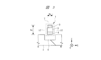
- FIG. 2 is a schematic cross sectional view of the beam type resonator taken along the line AA ′ in FIG. 1
- FIG. 3 is a beam along the line BB ′ in FIG. It is a cross-sectional schematic diagram of a type resonator.
- the beam type resonator is formed on the insulating substrate 2.
- the vibrating part 1 of this beam type resonator includes a piezoelectric thin film 5 (film thickness hp), a pair of upper metal films (upper electrodes) 3 (film thickness hd) and a lower part sandwiching a part of the piezoelectric thin film 5. It has a laminated structure (thickness ha) including a metal film (lower electrode) 4 (film thickness hu).
- the thickness ha is, for example, about 1 to 2 ⁇ m.
- the upper surface of the vibration unit 1 is surrounded by an upper elastic wave reflector (upper acoustic reflector) 7, the lower surface is surrounded by a lower elastic wave reflector (lower acoustic reflector) 6, and the side surface is a side elastic wave reflector (side). Part acoustic reflector) 12.
- both the upper metal film 3 and the lower metal film 4 are formed of an aluminum film formed by a film forming apparatus, and the piezoelectric thin film 5 is formed by a film forming apparatus and is formed of an aluminum nitride film.
- a thin film made of another conductive material for example, a conductive material such as copper, platinum, ruthenium, molybdenum, tungsten, or gold may be used. It goes without saying that it is good.
- piezoelectric thin film 5 instead of the aluminum nitride film, other piezoelectric materials such as zinc oxide, lithium niobate, lithium tantalate, potassium niobate, tantalum pentoxide, lead titanate or barium titanate are used. Needless to say, a thin film made of a material having a property may be used.
- the film formation apparatus described in Embodiment 1 is an apparatus typified by a sputtering apparatus, a vapor deposition apparatus, or a CVD apparatus, in which molecules, atoms, ions, or clusters thereof are directly stacked on a substrate.
- it is an apparatus for forming a thin film by laminating with a chemical reaction.
- the thin film described in the first embodiment is a film formed by this film forming apparatus, and is formed by a sintered body prepared by sintering, a hydrothermal synthesis method, a chocolate ski method, or the like. Bulk bodies are not included regardless of thickness.
- the upper metal film 3 In order to apply an electric field to the piezoelectric thin film 5, the upper metal film 3 substantially faces the corresponding lower metal film 4 across the piezoelectric thin film 5 in the vibration unit 1.
- the planar shapes do not necessarily match.
- the range in which the upper metal film 3 and the lower metal film 4 are opposed to each other in the planar shape is defined, and in the X-axis direction, the range in which the piezoelectric thin film 5 exists is defined as the Z-axis.
- the region from the lower surface of the upper elastic wave reflector 7 to the upper surface of the lower elastic wave reflector 6 is defined as the vibration unit 1.
- the first dimension (width Wa) in the X-axis direction of the vibration part 1 is set smaller than the third dimension (thickness ha) in the Z-axis direction.
- the second dimension (length La) in the Y-axis direction of the vibration unit 1 is set larger than the third dimension (thickness ha) in the Z-axis direction.
- the width Wa is, for example, about 0.6 ⁇ m
- the length La is, for example, about 100 ⁇ m. Therefore, the structure of the vibration part 1 is beam-like (a structure in which only one direction in the XYZ axis direction of the resonance part is sufficiently long), and this point is different from the structure of the vibration part of the conventional FBAR having a planar structure.
- the vibration unit 1 is physically connected to the end portion in the plus Y-axis direction and the end portion in the minus Y-axis direction indirectly by a fixed portion 8 made of the piezoelectric thin film 5.
- the fixing portion 8 may be configured to include the upper metal film 3 or the lower metal film 4 or may have another additional film.
- the lower elastic wave reflector 6 is not provided in the downward direction (minus Z-axis direction) of the fixed portion 8.
- the fixing portion 8 is physically connected to the insulating substrate 2 via the lower metal film 4 in the minus Y-axis direction, and directly connected to the insulating substrate 2 in the plus Y-axis direction.
- the insulating substrate 2 Since the insulating substrate 2 is sufficiently larger than the vibration part 1, it does not vibrate. In some cases, the vibration of the vibration part 1 flows into the insulating substrate 2, but even in this case, the amplitude of the insulating substrate 2 is sufficiently smaller than the amplitude of the vibration part 1 because it diffuses throughout the insulating substrate 2.
- the fixing part 8 is formed of a piezoelectric thin film 5 which is a main vibration medium of the vibration part 1. Therefore, the vibration of the surface of the fixed portion 8 on the vibration portion 1 side (the cross section of the fixed portion 8 on the vibration portion 1 side in FIG. 2) leaks to the insulating substrate 2. Further, since the insulating substrate 2 is sufficiently larger than the fixing portion 8 or the vibrating portion 1, the fixing portion 8 substantially functions as a mechanical fixing portion.
- the vibration part 1 vibrates.
- the Z-axis vibration and the X-axis vibration are 180 degrees out of phase.
- this vibration mode is referred to as a TWE mode (Thickness-Width Extensional mode).
- the vibration in the Y-axis direction of the vibration part 1 is a vibration unrelated to the main vibration, and thus causes a decrease in k2 in the TWE mode.
- spurious resonance occurs due to the electrical characteristics of the resonator.
- the vibration part 1 is sandwiched between the fixing parts 8 in both the positive Y-axis direction and the negative Y-axis method, and thus does not expand and contract in the Y-axis direction.
- the vibration in the Y-axis direction of the vibration unit 1 is not coupled to the vibration in the Z-axis direction or the vibration in the X-axis direction because the frequency is significantly different from the vibration in the Z-axis direction and the vibration in the X-axis direction.
- the optimum ratio of the width Wa to the thickness ha at which k2 is the largest is the absolute value (
- FIG. 4 is a schematic diagram for explaining a model used for calculation.
- the piezoelectric thin film 5 is a rectangular parallelepiped having a width W in the X-axis direction, a thickness h (1 ⁇ m) in the Z-axis direction, and a length L in the Y-axis direction. Further, both end surfaces in the Y-axis direction are mechanical fixing surfaces 9 as surfaces of the fixing portion 8 on the vibrating portion 1 side.
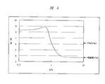
- FIG. 5 is a graph showing the relationship between k2 and W / h of the beam type resonator according to the first embodiment.
- a c-axis oriented aluminum nitride film was used as the piezoelectric thin film 5.
- the thicknesses of the upper metal film 3 and the lower metal film 4 are ignored, and the length L is sufficiently longer (infinite length) than the thickness h.
- the fixed surface 9 is also infinitely far away, since the vibration unit 1 is in contact with the fixed surface 9, vibration in the Y-axis direction does not occur.
- FIG. 5 shows that k2 larger than FBAR can be obtained by making W / h smaller than 1.05. Further, k2 larger than the width vibration can be obtained at all W / h. From FIG. 5, it is considered that W / h is in an appropriate range of, for example, 0.1 to 1.05 (which is not limited to this range depending on other conditions). A range suitable for mass production is 0.2 to 0.9, but a peripheral range centered on 0.6 such as 0.3 to 0.88 is considered most suitable.
- the ratio of the width Wa to the thickness ha (Wa / ha) of the vibration unit 1 is made smaller than 1.05, so that the beam-type resonance having k2 larger than FBAR. Can be provided.
- FIGS. 6 is a schematic top view of the beam-type resonator
- FIG. 7 is a schematic cross-sectional view of the beam-type resonator along the line CC ′ in FIG. 6
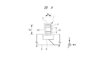
- FIG. 8 is a beam along the line DD ′ in FIG. It is a cross-sectional schematic diagram of a type resonator.
- the beam type resonator is formed on the insulating substrate 2.
- the vibration part 1 of this beam type resonator has the same shape as the vibration part 1 of the first embodiment described above.
- the widths of the piezoelectric thin film 5 and the upper metal film 3 of the vibration unit 1 are made to coincide with each other, but the effect of the invention is not affected.
- the acoustic insulation unit 10 is physically connected between the vibration unit 1 and the fixed unit 8.
- the vibration part 1 and the acoustic insulation part 10 or the acoustic insulation part 10 and the fixed part 8 do not necessarily have to be directly connected, but may be physically connected via another structure.
- the acoustic insulating portion 10 includes an upper metal film 3, a piezoelectric thin film 5, and a lower metal film 4.
- the upper metal film 3 of the acoustic insulation part 10 in the plus Y-axis direction and the lower metal film 4 of the acoustic insulation part 10 in the minus Y-axis direction also serve as electrical lead lines.
- the width Wb (fourth dimension) along the X-axis direction of the acoustic insulating portion 10 is set to, for example, 0.8 ⁇ m
- the length Lb along the Y-axis direction is set to, for example, 10 ⁇ m.
- the natural resonance frequency of the acoustic insulation unit 10 is set lower than the natural resonance frequency of the vibration unit 1.
- the natural resonance frequency of the vibration unit 1 is the series resonance frequency of the TWE mode of the vibration unit 1.
- the natural resonance frequency of the acoustic insulation unit 10 is a resonance frequency when the acoustic insulation unit 10 vibrates in the TWE mode.
- electrodes are present on the upper and lower surfaces, when the upper and lower electrodes are electrically short-circuited, this corresponds to the series resonance frequency when an AC voltage is applied to the upper and lower electrodes, and the upper and lower electrodes are When electrically open, it corresponds to the parallel resonance frequency when an AC voltage is applied to the upper and lower electrodes.
- electrodes are provided on the upper and lower surfaces, and the electrodes on the upper and lower surfaces are electrically short-circuited.
- FIG. 9 and 10 are graphs for explaining the behavior of the TWE mode of the vibration unit and the acoustic insulation unit according to the second embodiment.
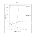
- FIG. 9 is a graph showing a TWE mode dispersion curve (ky real surface) of a beam-type resonator in which the width W of the vibrating part or the acoustic insulating part is 0.6 ⁇ m, the length L is 100 ⁇ m, and the thickness h is 1 ⁇ m. It is.
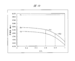
- FIG. 10 is a graph showing the width W dependence of the frequencies fd, fb, and ft shown in FIG.
- the frequency of the TWE mode decreases and increases again via the minimum.
- ky becomes 0, and changes to another mode near the frequency of 6020 MHz via the complex surface of ky and appears again on the real surface of ky.
- the TWE mode (shown by a broken line in the figure) in the region where ky is large is weakly coupled to the excitation electrode, the TWE mode is excited only in the frequency fd to frequency fb range shown by the solid line in FIG. Or vibrate. That is, the range from the frequency fd to the frequency fb is an acoustic propagation frequency band.
- no mode can be excited, vibrated or propagated between the frequency fb and the frequency ft. Therefore, the frequency between the frequency fb and the frequency ft is an acoustic insulation frequency band.
- the TWE mode having a ky of 0 or its vicinity is used.
- the resonance frequency substantially coincides with the frequency fb or slightly shifts to a lower frequency side than the frequency fb.
- this shift amount depends on the length L, when L / h >> 1, the slope when the KY of the TWE mode is 0 is zero, and thus the amount is negligible.
- L / h >> 1 the resonance frequency substantially coincides with the frequency fb.
- the resonance frequency shifts to a lower frequency side than the frequency fb. The frequency becomes between.
- the present inventors pay attention to the fact that the TWE mode has a vibration component in the X-axis direction, unlike the conventional FBAR, and a method for efficiently confining vibration energy in the vibration part 1, and the fixed part 8 and the vibration part.
- One physical or electrical connection method was examined in detail. As a result, in the TWE mode, it was found that when W / h is changed, the frequency fb is changed correspondingly. Utilizing this, by disposing the acoustic insulation part 10 having a width Wb larger than the vibration part 1 between the vibration part 1 and the fixed part 8, vibration energy can be confined in the vibration part 1, and The inventors have found that the insulating substrate 2 can be physically and firmly connected. Hereinafter, the effect of the acoustic insulating unit 10 will be described in detail.
- FIG. 10 is a graph showing the width W dependency of the frequencies fb and ft according to the second embodiment.
- the width W is increased, the frequency ft hardly changes, whereas the frequency fb moves to the low frequency side. Since the frequency between the frequency fb and the frequency ft functions as an acoustic insulation frequency, increasing the width W increases the acoustic insulation frequency band.
- the vibration unit 1 vibrates at the vibration frequency fb1. Since the acoustic insulation frequency of the acoustic insulation unit 10 is a frequency between the vibration frequency fb2 and the frequency ft, and fb2 ⁇ fb1 ⁇ ft, vibration energy of the vibration unit 1 cannot enter the acoustic insulation unit 10. Since the frequency ft is not dependent on the width W, by making the width Wb of the acoustic insulating portion 10 larger than the width Wa of the vibrating portion 1, it is always possible to satisfy fb2 ⁇ fb1 ⁇ ft. Therefore, the acoustic insulating unit 10 has a function of acoustically insulating the vibrating unit 1 and the fixed unit 8.
- the vibrating unit 1 is surrounded by elastic wave reflectors 6, 7, and 12 in the Z-axis direction and the X-axis direction, and the acoustic insulating unit 10 in the Y-axis direction. Therefore, in the second embodiment, elastic energy can be confined in the vibration part 1.
- the acoustic insulating unit 10 is installed between the vibrating unit 1 and the fixed unit 8, and the width Wb of the acoustic insulating unit 10 is set to be equal to that of the vibrating unit 1.
- the width Wb of the acoustic insulating unit 10 is set to be equal to that of the vibrating unit 1.
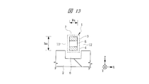
- FIGS. 11 is a schematic top view of the beam-type resonator
- FIG. 12 is a schematic cross-sectional view of the beam-type resonator along the line EE ′ in FIG. 11
- FIG. 13 is a beam along the line FF ′ in FIG. It is a cross-sectional schematic diagram of a type resonator.
- the beam-type resonator according to the third embodiment has the same shape as the beam-type resonator according to the second embodiment except for the fixed portion 8 and the acoustic insulating portion 10.
- the acoustic insulating unit 10 is composed of the upper metal film 3 and the piezoelectric thin film 5, or the piezoelectric thin film 5 and the lower metal film 4.
- the fixing portion 8 is composed of the upper metal film 3 and the piezoelectric thin film 5, or the piezoelectric thin film 5 and the lower metal film 4.
- the upper metal film 3 of the acoustic insulation part 10 in the plus Y-axis direction and the lower metal film 4 of the acoustic insulation part 10 in the minus Y-axis direction also serve as electrical lead lines. Further, the width Wb along the X-axis direction of the acoustic insulating portion 10 is set to, for example, 0.9 ⁇ m, and Lb along the Y-axis direction is set to, for example, 10 ⁇ m.
- FIG. 14 is a graph showing the width W dependence of the frequencies fb and ft of the acoustic insulation unit 10 according to the third embodiment. Since the upper metal film 3 or the lower metal film 4 is not provided, the vibration frequency fb3 is shifted to the higher frequency side than the vibration frequency fb1 of the second embodiment described above. For easy understanding, the vibration frequency fb1 of the vibration part 1 is shown in FIG.
- the vibration unit 1 vibrates at the vibration frequency fb1. Since the acoustic insulation frequency of the acoustic insulation unit 10 is a frequency between the vibration frequency fb3 and the frequency ft and fb3 ⁇ fb1 ⁇ ft, the vibration energy of the vibration unit 1 cannot enter the acoustic insulation unit 10. Therefore, the acoustic insulation unit 10 has a function of acoustically insulating the vibration unit 1 and the fixed unit 8.
- the vibrating unit 1 is surrounded by elastic wave reflectors 6, 7, and 12 in the Z-axis direction and the X-axis direction, and the acoustic insulating unit 10 in the Y-axis direction. Therefore, also in the third embodiment, elastic energy can be confined in the vibration part 1.
- the acoustic insulation unit 10 is installed between the vibration unit 1 and the fixed unit 8, and the acoustic insulation is performed.
- the width Wb of the portion 10 is set to a value larger than the width Wa of the vibrating portion 1, elastic energy can be confined in the resonance portion.
- FIGS. 15 is a schematic top view of the beam-type resonator
- FIG. 16 is a schematic cross-sectional view of the beam-type resonator along the line GG ′ in FIG.
- FIG. 17 is a beam along the line HH ′ in FIG. It is a cross-sectional schematic diagram of a type resonator.
- the beam type resonator is formed on the insulating substrate 2.
- the vibration part 1 of this beam type resonator has the same shape as the vibration part 1 according to the second embodiment described above.
- the acoustic insulation unit 10 has the same shape as the acoustic insulation unit 10 according to the second embodiment.
- the phase rotation unit 11 is physically connected between the vibration unit 1 and the acoustic insulation unit 10.
- the vibration unit 1 and the phase rotation unit 11 or the phase rotation unit 11 and the acoustic insulation unit 10 do not necessarily have to be directly connected, but may be physically connected via another structure.
- the phase rotation unit 11 is composed of an upper metal film 3, a piezoelectric thin film 5, and a lower metal film 4.
- the upper metal film 3 of the phase rotation unit 11 in the plus Y-axis direction and the lower metal film 4 of the phase rotation unit 11 in the minus Y-axis direction also serve as electrical lead lines.
- the width Wp (fifth dimension) along the X-axis direction of the phase rotating unit 11 is set to 0.4 ⁇ m, for example, and the length Lp along the Y-axis direction is set to 1.2 ⁇ m, for example.
- the natural resonance frequency of the phase rotation unit 11 is set to be larger than 1 time and smaller than 1.05 times the natural resonance frequency of the vibration unit 1.
- the natural resonance frequency of the phase rotation unit 11 is a resonance frequency when the phase rotation unit 11 vibrates in the TWE mode.
- the upper and lower electrodes When electrodes are present on the upper and lower surfaces, when the upper and lower electrodes are electrically short-circuited, this corresponds to the series resonance frequency when an AC voltage is applied to the upper and lower electrodes, and the upper and lower electrodes are When electrically open, it corresponds to the parallel resonance frequency when an AC voltage is applied to the upper and lower electrodes.
- electrodes are provided on the upper and lower surfaces, and the electrodes on the upper and lower surfaces are electrically short-circuited.
- the present inventors pay attention to the fact that the TWE mode has a vibration component in the X-axis direction, which is different from the conventional FBAR, and a method for setting the vibration mode of the vibration unit 1 to the piston mode, and the acoustic insulation unit 10 and the vibration.
- the physical connection method with the part 1 was examined in detail. As a result, it has been found that in the TWE mode, when the width W is changed, the frequency fd is also changed correspondingly. It has also been found that the rate of change of the frequency fd is substantially equal to the rate of change of the frequency fb.
- the vibration mode of the vibration unit 1 is changed to the piston mode. And it has been found that it can be physically and firmly connected to the insulating substrate 2.
- the effect of the phase rotation unit 11 will be described in detail.
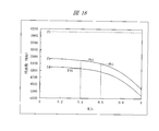
- FIG. 18 is a diagram showing the width W dependency of the frequencies fd and fb of the phase rotation unit 11 according to the fourth embodiment. For easy understanding, the vibration frequency fb1 of the vibration part 1 is shown in FIG.
- the vibration unit 1 vibrates at the vibration frequency fb1.
- the acoustic propagation frequency of the phase rotation unit 11 is a frequency between the vibration frequency fd4 and the vibration frequency fb4.
- the vibration frequency fd4 is about 0.95 times the vibration frequency fb4.
- fd4 ⁇ fb1 ⁇ fb4 can be achieved by making the width Wp of the phase rotation unit 11 smaller than the width Wa of the vibration unit 1. Since fd4 ⁇ fb1 ⁇ fb4, the elastic wave of the vibration unit 1 enters the phase rotation unit 11 and propagates to the acoustic insulation unit 10.
- the phase rotation unit 11 has a function of controlling the phase of the elastic wave coming out of the vibration unit 1 and the returning elastic wave.
- the phase of the elastic wave rotates 180 degrees. Therefore, by rotating the phase of the elastic wave by 90 degrees (reciprocating 180 degrees) by the phase rotating unit 11, the vibration form of the vibrating unit 1 is changed to the piston. Can be in mode.
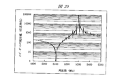
- FIG. 19 and 20 are graphs showing the effect of the phase rotation unit 11 according to the fourth embodiment.
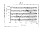
- FIG. 19 is a graph showing impedance characteristics of the beam type resonator according to the fourth embodiment.
- FIG. 20 is a graph showing the impedance characteristics of a beam-type resonator in which the width Wp of the phase rotating unit 11 is matched with the width Wa of the vibrating unit 1 for comparison.
- the vibration mode of the vibration unit 1 is the piston mode, the excitation of spurious can be suppressed.
- the phase rotation unit 11 is installed between the vibration unit 1 and the acoustic insulation unit 10, and the width Wp of the phase rotation unit 11 is set to be the vibration unit.
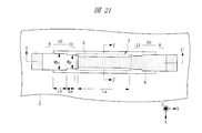
- FIGS. 21 is a schematic top view of the beam-type resonator
- FIG. 22 is a schematic cross-sectional view of the beam-type resonator along the line II ′ in FIG. 21
- FIG. 23 is a beam along the line JJ ′ in FIG. It is a cross-sectional schematic diagram of a type resonator.
- the beam-type resonator according to the fifth embodiment has the same shape as the beam-type resonator according to the above-described fourth embodiment except for the phase rotating unit 11.
- the phase rotation unit 11 includes the upper metal film 3 and the piezoelectric thin film 5 or the piezoelectric thin film 5 and the lower metal film 4.
- the upper metal film 3 of the phase rotation unit 11 on the plus Y-axis direction side and the lower metal film 4 of the phase rotation unit 11 on the minus Y-axis direction side also serve as electrical lead lines.
- the width Wp along the X-axis direction of the phase rotation unit 11 is set to 0.7 ⁇ m, for example, and Lp along the Y-axis direction is set to 1.0 ⁇ m, for example.
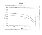
- FIG. 24 is a graph showing the width W dependency of the frequencies fd and fb of the phase rotation unit 11 according to the fifth embodiment. Since the upper metal film 3 or the lower metal film 4 is not provided, the vibration frequency fb5 is shifted to a higher frequency side than the vibration frequency fb4 of the fourth embodiment described above. For easy understanding, the vibration frequency fb1 of the vibration part 1 is shown in FIG.
- the natural resonance frequency of the phase rotation unit 11 is set to be larger than 1 time and smaller than 1.05 times the natural resonance frequency of the vibration unit 1.
- the vibration unit 1 vibrates at the vibration frequency fb1.
- the acoustic propagation frequency of the phase rotation unit 11 is a frequency between the vibration frequency fd5 and the vibration frequency fb5.
- the vibration frequency fd5 is about 0.95 times the vibration frequency fb5. Since fd5 ⁇ fb1 ⁇ fb5, the same effect as in the fourth embodiment described above, that is, the vibration mode of the vibration unit 1 can be set to the piston mode. In the fifth embodiment, since the vibration mode of the vibration unit 1 is the piston mode, the excitation of spurious can be suppressed.
- the phase rotating unit 11 is installed between the vibrating unit 1 and the acoustic insulating unit 10 to vibrate.
- the width Wa of the unit 1 and the width Wp of the phase rotation unit 11 are different values for the width Wa of the unit 1 and the width Wp of the phase rotation unit 11 and setting the resonance frequency of the phase rotation unit 11 to be higher than the resonance frequency of the vibration unit 1, a beam type resonator without spurious is provided. be able to.
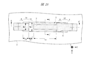
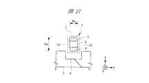
- FIGS. 25 is a schematic top view of the beam-type resonator
- FIG. 26 is a schematic cross-sectional view of the beam-type resonator along the line KK ′ in FIG. 25
- FIG. 27 is a beam along the line LL ′ in FIG. It is a cross-sectional schematic diagram of a type resonator.
- the beam type resonator is formed on the insulating substrate 2.
- the beam-type resonator includes a vibration unit 1, a phase rotation unit 11, an acoustic insulation unit 10, and a fixed unit 8.
- a phase rotation unit 11 is physically connected between the vibration unit 1 and the acoustic insulation unit 10.
- the fixed portion 8 is physically connected between the acoustic insulating portion 10 and the insulating substrate 2.
- the vibrating part 1 is composed of an upper metal film 3, a piezoelectric thin film 5, and a lower metal film 4.
- the piezoelectric thin film 5 is sandwiched between the upper metal film 3 and the lower metal film 4.
- the upper metal film 3 and the lower metal film 4 are made of a thin film mainly composed of aluminum having a thickness of 0.1 ⁇ m, for example.
- the piezoelectric thin film 5 is made of, for example, a thin film whose main component is aluminum nitride having a C-axis orientation with a thickness of 1 ⁇ m.
- the direction of the C axis is a direction perpendicular to the insulating substrate 2.
- the width Wa of the vibration part 1 is, for example, 0.6 ⁇ m
- the length La is, for example, 100 ⁇ m
- the widths of the upper metal film 3, the piezoelectric thin film 5, and the lower metal film 4 are the same.
- the phase rotation unit 11 is composed of the piezoelectric thin film 5 and the lower metal film 4, or the upper metal film 3 and the piezoelectric thin film 5.
- the upper metal film 3 and the lower metal film 4 are made of a thin film mainly composed of aluminum having a thickness of 0.1 ⁇ m, for example.
- the piezoelectric thin film 5 is made of, for example, a thin film whose main component is aluminum nitride having a C-axis orientation with a thickness of 1 ⁇ m.
- the direction of the C axis is a direction perpendicular to the insulating substrate 2.
- the width Wp of the phase rotation unit 11 is, for example, 0.96 ⁇ m, the length Lp is, for example, 1.6 ⁇ m, and the widths of the piezoelectric thin film 5 and the lower metal film 4 are the same.
- the acoustic insulating portion 10 includes an upper metal film 3, a piezoelectric thin film 5, and a lower metal film 4.
- the piezoelectric thin film 5 is sandwiched between the upper metal film 3 and the lower metal film 4.
- the upper metal film 3 and the lower metal film 4 are made of a thin film mainly composed of aluminum having a thickness of 0.1 ⁇ m, for example.
- the piezoelectric thin film 5 is made of, for example, a thin film whose main component is aluminum nitride having a C-axis orientation with a thickness of 1 ⁇ m.
- the direction of the C axis is a direction perpendicular to the insulating substrate 2.
- the width Wb of the acoustic insulating portion 10 is, for example, 0.8 ⁇ m, the length Lb is, for example, 10 ⁇ m, and the widths of the upper metal film 3, the piezoelectric thin film 5, and the lower metal film 4 are the same.
- the two acoustic insulating portions 10 are electrically connected at different portions from the acoustic insulating portion 10 so that the upper metal film 3 and the lower metal film 4 are equipotential.
- the fixing portion 8 is composed of an upper metal film 3, a piezoelectric thin film 5, and a lower metal film 4.
- the piezoelectric thin film 5 is sandwiched between the upper metal film 3 and the lower metal film 4.
- the upper metal film 3 and the lower metal film 4 are made of a thin film mainly composed of aluminum having a thickness of 0.1 ⁇ m, for example.
- the piezoelectric thin film 5 is made of, for example, a thin film whose main component is aluminum nitride having a C-axis orientation with a thickness of 1 ⁇ m.
- the direction of the C axis is a direction perpendicular to the insulating substrate 2.
- the two fixing portions 8 are electrically connected so that the upper metal film 3 and the lower metal film 4 are equipotential, respectively.
- the insulating substrate 2 is composed of a silicon single crystal substrate and a silicon oxide film having a thickness of 1 ⁇ m formed on the surface thereof. By forming a silicon oxide film on the surface, the silicon single crystal substrate functions as an electrically insulating substrate.
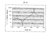
- FIG. 28 is a graph showing impedance characteristics of the beam-type resonator according to the sixth embodiment. Since aluminum is used as the electrode material, k2 is 9.44%, which is larger than the value shown in FIG.
- the vibration unit 1, the phase rotation unit 11, the acoustic insulation unit 10, and the fixing unit 8 are all configured by the upper metal film 3, the piezoelectric thin film 5, and the lower metal film 4 having the same film thickness.
- the resonator can be formed by three film formation steps, and for example, energy confinement and piston mode excitation can be realized with fewer steps than the known technique disclosed in Patent Document 2. it can. As a result, a beam type resonator having low loss and no spurious can be provided at low cost.
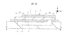
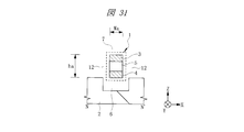
- FIGS. 29 is a schematic top view of the beam-type resonator
- FIG. 30 is a schematic cross-sectional view of the beam-type resonator along the line MM ′ in FIG. 29
- FIG. 31 is a beam along the line NN ′ in FIG. It is a cross-sectional schematic diagram of a type resonator.
- the beam type resonator is formed on the insulating substrate 2.
- the beam-type resonator includes a vibration unit 1, a phase rotation unit 11, an acoustic insulation unit 10, and a fixed unit 8.
- a phase rotation unit 11 is physically connected between the vibration unit 1 and the acoustic insulation unit 10.
- the fixed portion 8 is physically connected between the acoustic insulating portion 10 and the insulating substrate 2.
- the vibrating part 1 is composed of an upper metal film 3, a piezoelectric thin film 5, and a lower metal film 4.
- the piezoelectric thin film 5 is sandwiched between the upper metal film 3 and the lower metal film 4.
- the upper metal film 3 and the lower metal film 4 are made of a thin film mainly composed of molybdenum having a thickness of 0.1 ⁇ m, for example.
- the piezoelectric thin film 5 is made of, for example, a thin film whose main component is aluminum nitride having a C-axis orientation with a thickness of 1 ⁇ m.
- the direction of the C axis is a direction perpendicular to the insulating substrate 2.
- the width Wa of the vibrating part 1 is, for example, 0.6 ⁇ m
- the length La is, for example, 100 ⁇ m
- the widths of the upper metal film 3, the piezoelectric thin film 5, and the lower metal film 4 are the same.
- the phase rotation unit 11 is composed of an upper metal film 3, a piezoelectric thin film 5, and a lower metal film 4.
- the lower metal film 4 is made of a thin film mainly composed of molybdenum having a thickness of 0.1 ⁇ m, for example.
- the piezoelectric thin film 5 is made of, for example, a thin film whose main component is aluminum nitride having a C-axis orientation with a thickness of 1 ⁇ m.
- the direction of the C axis is a direction perpendicular to the insulating substrate 2.
- the width Wp of the phase rotation unit 11 is 0.4 ⁇ m, for example, and the length Lp is 3.5 ⁇ m, for example, and the widths of the piezoelectric thin film 5 and the lower metal film 4 are the same.
- the acoustic insulating portion 10 is composed of the upper metal film 3 and the piezoelectric thin film 5, or the piezoelectric thin film 5 and the lower metal film 4.
- the upper metal film 3 and the lower metal film 4 are formed of a thin film mainly composed of, for example, 0.1 ⁇ m molybdenum.
- the piezoelectric thin film 5 is made of, for example, a thin film whose main component is aluminum nitride having a C-axis orientation with a thickness of 1 ⁇ m.
- the direction of the C axis is a direction perpendicular to the insulating substrate 2.
- the width Wb of the acoustic insulating unit 10 is, for example, 1.4 ⁇ m, the length Lb is, for example, 10 ⁇ m, and the widths of the upper metal film 3, the piezoelectric thin film 5, and the lower metal film 4 are the same.
- the fixing part 8 is composed of the upper metal film 3, the piezoelectric thin film 5 and the lower metal film 4, or the piezoelectric thin film 5 and the lower metal film 4.
- the piezoelectric thin film 5 is sandwiched between the upper metal film 3 and the lower metal film 4.
- the upper metal film 3 and the lower metal film 4 are made of a thin film mainly composed of molybdenum having a thickness of 0.1 ⁇ m, for example.
- the piezoelectric thin film 5 is made of, for example, a thin film whose main component is aluminum nitride having a C-axis orientation with a thickness of 1 ⁇ m.
- the direction of the C axis is a direction perpendicular to the insulating substrate 2.
- the upper metal film 3 and the lower metal film 4 are electrically connected so as to be equipotential.
- the insulating substrate 2 is composed of a silicon single crystal substrate and a silicon oxide film having a thickness of 1 ⁇ m formed on the surface thereof. By forming a silicon oxide film on the surface, the silicon single crystal substrate functions as an electrically insulating substrate.
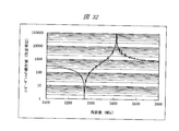
- FIG. 32 is a graph showing impedance characteristics of the beam-type resonator according to the seventh embodiment. Since heavy molybdenum is used as the electrode material, k2 is 9.73%, which is a value larger than the value shown in the sixth embodiment. Similarly to the sixth embodiment described above, all of the vibration unit 1, the phase rotation unit 11, the acoustic insulation unit 10, and the fixing unit 8 are the upper metal film 3, the piezoelectric thin film 5, and the lower metal film 4 having the same film thickness. It is configured. As a result, the resonator can be formed in three film formation steps, and for example, energy confinement and piston mode excitation can be realized with fewer steps than the known technique disclosed in Patent Document 2. . As a result, a beam type resonator having low loss and no spurious can be provided at low cost.
- the resonator according to the eighth embodiment is a modification of the seventh embodiment described above. That is, the fixed portion 8 is spatially located in the minus X-axis direction of the vibrating portion 1 but physically connected indirectly to the plus Y-axis direction and the minus Y-axis direction of the vibrating portion 1. Yes. Thereby, it has the same function as the seventh embodiment described above.
- FIG. 34 is a schematic top view of the beam type resonator
- FIG. 35 is a graph showing impedance characteristics of the beam type resonator.
- the phase rotation unit 11 has the same shape as the phase rotation unit 11 of the seventh embodiment described above.
- the vibration part 1 is composed of the upper metal film 3, the piezoelectric thin film 5, and the lower metal film 4 as in the vibration part 1 of the seventh embodiment.
- the width Wa of the vibration part 1 is, for example, 0.6 ⁇ m
- the length La is, for example, 50 ⁇ m
- the upper metal film 3, the piezoelectric thin film 5, and the lower metal film 4 have the same width.
- the acoustic insulating portion 10 is composed of the upper metal film 3 and the piezoelectric thin film 5 or the piezoelectric thin film 5 and the lower metal film 4 as in the seventh embodiment.
- the width Wb of the acoustic insulating portion 10 is, for example, 1.9 ⁇ m, the length Lb is, for example, 10 ⁇ m, and the widths of the upper metal film 3, the lower metal film 4, and the piezoelectric thin film 5 are the same.
- the beam-type resonator exhibits electric characteristics similar to those of the seventh embodiment described above. Since the vibration frequencies of the two vibrating parts 1 are within the insulating frequency range of the acoustic insulating part 10, the acoustic insulating part 10 performs the same function as the acoustic insulating part 10 of the seventh embodiment described above. Even when a plurality of vibrating parts 1 are connected to one acoustic insulating part 10, the effect of the invention does not change.
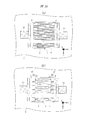
- FIG. 36A is a schematic top view of a first example of a beam-type resonator group in which a large number of beam-type resonators shown in the first embodiment are connected in parallel
- FIG. It is a top schematic diagram of the 2nd example of the beam type resonator group which connected many beam type resonators shown in the form 7 in parallel.
- a beam type resonator group in which a plurality of the beam type resonators described in the seventh embodiment are connected in parallel will be described.
- a plurality of beam-type resonators are formed on one lower elastic wave reflector 6. These beam type resonators share one fixed portion 8. All the beam resonators are electrically connected to one fixed portion 8 and connected to a common input / output terminal 13. In addition, the acoustic insulating unit 10 and the fixed unit 8 are physically connected via the connection unit 14. Since the lower elastic wave reflector 6 is shared by a plurality of beam type resonators, many beam type resonators can be arranged on the chip. Therefore, the chip can be reduced in size.
- an impedance element such as a resonator
- a high-frequency electrical component such as a high-frequency filter
- the characteristic impedance can be freely set between the components, but if it is too low, the electrical resistance loss becomes large, and if it is too high, the voltage amplitude exceeds the power supply voltage, so it is generally set to 50 to 200 ⁇ .
- an arbitrary characteristic impedance can be realized by adjusting the number of beam type resonators connected in parallel.
- FIG. 37 is a circuit diagram of a high-pass filter using the beam-type resonator according to the tenth embodiment.
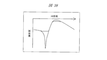
- a plurality of beam type resonators 15 are electrically connected to the parallel arm between the two input / output terminals 13. Since the beam type resonator 15 has a small elastic energy leakage, the resistance value becomes almost zero at the series resonance frequency, and the resistance value becomes almost infinite at the parallel resonance frequency. Therefore, in the pass characteristic, an attenuation pole is formed at the series resonance frequency, and a minimum pass loss point is formed at the parallel resonance frequency.
- FIG. 38 is a graph for explaining pass characteristics of a low-pass filter in which the widths of all the vibration parts of the beam-type resonator according to the tenth embodiment are set to be the same.
- the beam type resonator has a large k2, a small leakage of elastic energy, and no spurious. Thereby, it is possible to widen the attenuation frequency band and the passing frequency band, and it is possible to realize a passing characteristic with a large attenuation amount between them, a small loss amount, and further without spurious.
- FIG. 39 is a graph illustrating the pass characteristics of the low-pass filter in which the width of each vibration part of the beam resonator according to the tenth embodiment described above is set to different values (seven types).
- the present inventors paid attention to the fact that the TWE mode has a vibration component in the X-axis direction, unlike the conventional FBAR, and examined in detail the relationship between the series resonance frequency or parallel resonance frequency and the shape of the vibration part.
- the TWE mode it has been found that when the width W of the vibration part is changed, the series resonance frequency and the parallel resonance frequency change correspondingly.
- a low-pass filter having a plurality of attenuation poles can be realized by connecting a plurality of beam-type resonators having different widths W of the vibrating portion in parallel. This will be described in detail below with reference to FIG.
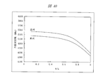
- FIG. 40 is a graph for explaining the relationship between the series resonance frequency or the parallel resonance frequency and the width W dependency of the vibration part.
- the series resonance frequency and the parallel resonance frequency move to the low frequency side.
- the series resonance frequency and the parallel resonance frequency have a maximum interval near 0.7 ⁇ m, but simply decrease with almost the same tendency. Therefore, in the beam type resonator, the series resonance frequency and the parallel resonance are not changed according to the width W of the vibration part without changing the film thickness of the piezoelectric thin film, the upper metal film, and the lower metal film, and without adding a new film.
- the frequency can be adjusted.
- FIG. 41 is a circuit diagram of a low-pass filter in which a large number of beam-type resonators according to the first to tenth embodiments described above are connected in series.
- a plurality of beam type resonators 15 are electrically connected to the series arm between the two input / output terminals 13. Therefore, in the pass characteristic, a minimum pass loss point can be formed at the series resonance frequency, and an attenuation pole can be formed at the parallel resonance frequency.
- FIG. 42 is a graph illustrating the pass characteristics of a low-pass filter in which the widths of all the vibration parts of the beam type resonator according to the tenth embodiment described above are set to be the same.
- the beam type resonator has a large k2, a small leakage of elastic energy, and no spurious. Thereby, it is possible to widen the attenuation frequency band and the passing frequency band, and it is possible to realize a passing characteristic with a large attenuation amount between them, a small loss amount, and further without spurious.
- FIG. 43 is a graph illustrating the pass characteristics of the low-pass filter in which the width of each vibration part of the beam resonator according to the tenth embodiment described above is set to different values (seven types). It is possible to realize a pass characteristic in which the attenuation frequency band and the pass frequency band are further widened, the attenuation amount therebetween is larger, and the loss amount is smaller.
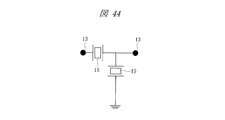
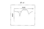
- FIG. 44 is a circuit diagram of a band-pass filter using the beam type resonator according to the first to tenth embodiments
- FIG. 45 is a graph illustrating the pass characteristics.
- One beam type resonator 15 is connected to the series arm between the two input / output terminals 13, and one beam type resonator 15 is electrically connected to the parallel arm.
- the width of the vibrating portion of the series arm is set to be narrower than that of the parallel arm.
- the film thicknesses of the piezoelectric thin film, the upper metal film, and the lower metal film are set to be the same.
- a plurality of beam-type resonators having different series resonance frequencies can be collectively manufactured by a common process. That is, a high frequency filter having excellent electrical characteristics can be provided at low cost.
- Embodiment 11 can be used, and similar effects can be obtained.
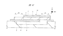
- FIGS. 46 is a schematic top view of the beam-type resonator
- FIG. 47 is a schematic cross-sectional view of the beam-type resonator along the line OO ′ in FIG. 46
- FIG. 48 is a schematic top view of the region P in FIG.
- a conventional FBAR 16 is formed on the insulating substrate 2. As shown in FIG.
- the FBAR 16 includes a piezoelectric thin film 5 and a pair of an upper metal film 3 and a lower metal film 4 that are present with the piezoelectric thin film 5 interposed therebetween.
- the structure of the FBAR 16 is a film (a structure in which the two directions in the XYZ-axis direction (X-axis direction and Y-axis direction) of the resonance portion are sufficiently long) and has a planar structure.
- the FBAR 16 is physically connected to the fixed portion 8 via the phase rotating portion 11 and the acoustic insulating portion 10 at both ends in the plus X-axis direction and the minus X-axis direction, and the plus Y-axis direction and the minus Y-axis direction. Yes.
- the phase rotation unit 11 is composed of the upper metal film 3 and the piezoelectric thin film 5 or the piezoelectric thin film 5 and the lower metal film 4. Further, the width Wp of the phase rotation unit 11 is set to 1.2 ⁇ m, for example, and the length Lp is set to 3.5 ⁇ m, for example.
- the natural resonance frequency of the FBAR 16 is a series resonance frequency of the FBAR 16.
- the thickness vibration mode of the FBAR 16 is mode-converted to the TWE mode. I found that I could enter 11. Further, it has been found that the TWE mode propagating through the phase rotation unit 11 cannot enter the acoustic insulation unit 10 by setting the natural resonance frequency of the acoustic insulation unit 10 lower than the natural resonance frequency of the FBAR 16.
- the natural resonance frequency of the FBAR 16 is about 10% higher than the natural resonance frequency of the TWE mode, as shown by the frequency fb in FIG.
- the phase rotation unit 11 includes the upper metal film 3 and the piezoelectric thin film 5, or the piezoelectric thin film 5 and the lower film.
- the metal film 4 is used. Furthermore, it is necessary to set the main vibration mode in the phase rotation unit 11 to the TWE mode.
- the main vibration mode in the acoustic insulation unit 10 may be set to the TWE mode.
- the phase rotation unit 11 includes the upper metal film 3 and the piezoelectric thin film 5, or the piezoelectric thin film 5 and the lower metal film 4.
- the upper metal film 3, the piezoelectric thin film 5, and the lower metal film 4 are included. You may comprise. In this case, it is desirable that the upper metal film 3 and the lower metal film 4 are electrically short-circuited in order to prevent excitation of the TWE mode in the acoustic insulating unit 10.
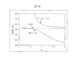
- FIG. 49 is a graph illustrating the width W dependence of the elastic mode of the acoustic insulation portion of the beam-type resonator according to the twelfth embodiment.
- the acoustic insulation portion includes a higher-order TWE mode that is observed as spurious. Since the higher-order TWE mode also has an acoustic propagation frequency band, it is desirable to eliminate the higher-order TWE mode in order for the acoustic insulation portion to function stably as an insulating layer.
- the natural resonance frequency of the TWE mode and the natural resonance frequency of the higher-order TWE mode are Never match. That is, by making W / h smaller than 2, the acoustic insulation portion can function as a stable acoustic insulation portion. Similarly, by making W / h smaller than 2, the phase rotating unit can function as a stable phase rotating unit.
- FIGS. 50 is a schematic top view of the beam-type resonator
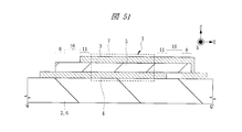
- FIG. 51 is a schematic cross-sectional view of the beam-type resonator along the line QQ ′ in FIG. 50
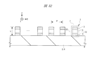
- FIG. 52 is a beam along the line RR ′ in FIG. It is a cross-sectional schematic diagram of a type resonator.
- a plurality of beam-type resonators are arranged in parallel.
- Each beam type resonator is arranged in the direction opposite to the voltage application direction of the adjacent beam type resonator.
- P ⁇ (f0 ⁇ ( Since Cij / p) 1/2 ) / 2 is set, the insulating substrate 2 functions as the lower acoustic wave reflector 6. Since the acoustic insulating portion 10 is formed on the surface of the insulating substrate 2, the acoustic insulating portion 10 also functions as the fixing portion 8.
- the manufacturing process of the lower acoustic wave reflector 6 can be omitted, and the beam type can be obtained at low cost.
- a resonator and a high-frequency filter using the resonator can be provided.
- FIG. 53 is a schematic top view of the high-frequency device
- FIG. 54 is an equivalent circuit diagram of the high-frequency device.
- FIGS. 53 and 54 As shown in FIGS. 53 and 54, four 100 ⁇ m square input / output terminals 13, four ground terminals 17, and a plurality of beam-type resonators 15 are arranged on a silicon chip having a silicon oxide film on the surface. ing.
- electrical connection lines are omitted, but in accordance with the equivalent circuit shown in FIG. 54, the beam type resonators 15 are electrically connected in a ladder type.
- the beam type resonator group shown in FIG. 53 includes the beam type resonators shown in the first to tenth embodiments. Therefore, the high-frequency device according to the fourteenth embodiment includes a large number of beam-type resonators 15.
- the beam-type resonators 15 do not necessarily have to have the same orientation, and can be arranged in an orientation that facilitates electrical connection. In addition, since each beam type resonator 15 does not leak elastic energy, each beam type resonator 15 can be arranged close to each other. As a result, many beam-type resonators 15 can be arranged on a small chip. That is, since the chip size of the high-frequency device can be reduced, a small and low-cost high-frequency device can be provided.
- the film thicknesses of the piezoelectric thin film and the electrode are described by taking a specific thickness as an example.
- the operating frequency or natural resonance frequency shifts, but the relative magnitude relationship between the frequencies fd, fb, and ft does not change. Therefore, the effect of the present invention is not limited to the film thickness.
- the width W, the length L, and the thickness h are meaningful in relative values, the effects of the present invention are not limited to specific dimensions.
- a single mode resonator configured by a pair of hot electrodes and a ground electrode has been described as an example, but configured by a plurality of hot electrodes.
- a typical multimode resonator can be realized, for example, by slitting the upper electrode near the center of the upper electrode. Further, it can be realized by connecting a part of the vibrating part 1 of the two beam type resonators close to each other by the piezoelectric thin film 5, the upper metal film 3, or the lower metal film 4.
- the vibration unit 1, the fixing unit 8, the acoustic insulation unit 10, and the phase rotation unit 11 are configured by the upper metal film 3, the piezoelectric thin film 5, and the lower metal film 4.
- a silicon oxide film is added between the upper metal film 3 and the piezoelectric thin film 5, between the piezoelectric thin film 5 and the lower metal film 4, or on the upper metal film 3 or below the lower metal film 4. May be. In this case, there is an effect of improving temperature stability. Further, an insulating film or a dissimilar metal film may be added under the lower metal film 4.
- the cavity as the lower acoustic wave reflector 6 can be stably formed, and the film quality of each of the upper metal film 3, the piezoelectric thin film 5, and the lower metal film 4 can be improved.
- the loss of the resonator can be further reduced.
- air is used as the acoustic reflector.
- This has a large difference in acoustic impedance between solid and air with respect to the TWE mode, and exhibits an almost 100% reflection coefficient at the interface, so that it functions as the most excellent acoustic reflector.
- the same effect can be obtained by using another gas or vacuum instead of air.
- k2 is slightly smaller than when air is used, and the manufacturing cost increases.
- the present invention can be applied to a piezoelectric acoustic wave resonator in which a resonance frequency is a high frequency of 10 MHz or more and a resonance part is formed of a thin film and an elastic wave device using the piezoelectric acoustic wave resonator.
- Vibrating part 2 Insulating substrate 3 Upper metal film (upper electrode) 4 Lower metal film (lower electrode) 5 Piezoelectric thin film 6 Lower elastic wave reflector (lower acoustic reflector) 7 Upper elastic wave reflector (Upper acoustic reflector) 8 Fixing part 9 Fixing surface 10 Acoustic insulating part 11 Phase rotating part 12 Side acoustic wave reflector (side acoustic reflector) 13 Input / output terminal 14 Connection 15 Beam type resonator 16 FBAR 17 Ground terminal
Landscapes
- Physics & Mathematics (AREA)
- Acoustics & Sound (AREA)
- Chemical & Material Sciences (AREA)
- Crystallography & Structural Chemistry (AREA)
- Piezo-Electric Or Mechanical Vibrators, Or Delay Or Filter Circuits (AREA)
Abstract
Description
非特許文献3において、特許文献1、2または非特許文献1、2に開示された弾性波共振器のk2(電気機械結合係数)が詳細に議論されている。非特許文献3によると、電極材料に重い金属を用いることによりk2を大きくすることができ、FBAR型のk2の方がSMR型のk2よりも大きいことが開示されている。さらに、k2が大きいほど高周波フィルタの電気特性は良くなるが、電極材料に重い金属を用いても、特許文献1、2または非特許文献1、2に開示された高周波用の弾性波共振器であるFBARやSMRは高々6.5~7%であることも開示されている。このため、さらに電気特性の良い高周波フィルタを実現するには、さらに大きいk2を有する共振器を用いることが必要であるが、FBAR及びSMRでは、さらなる高周波フィルタの電気特性の向上が望めない。
特許文献1または非特許文献1、2に開示された高周波用の弾性波共振器では、特許文献2に記載された現象、つまり面内方向の伸縮成分を有するスプリアス振動が微小に発生し、振動部(上部金属膜と圧電薄膜と下部金属膜とからなる三層構造を有し、かつ、その三層構造の上下部に音響反射器を有する部分)から圧電薄膜を伝わって弾性エネルギーが漏洩する現象が発生する。このため共振器のQ値が劣化し、またフィルタの損失が増加する。
特許文献1または非特許文献1、2に開示された高周波用の弾性波共振器では、特許文献2に記載された現象、つまり基本波以外にラム波も励振するため、スプリアス共振が発生する現象が発生する。このため共振器のQ値が劣化し、またフィルタの損失が増加する。
ラダー型に代表される弾性波共振器を用いたフィルタでは、直列腕共振器の共振周波数を並列腕共振器の共振周波数より高めることにより、帯域通過型フィルタを実現させている。このため異なる共振周波数を有する弾性波共振器を同一基板上に形成する必要がある。
本実施の形態1によるビーム型共振器を図1~図3を用いて説明する。図1はビーム型共振器の上面模式図、図2は図1のA-A′線に沿ったビーム型共振器の断面模式図、図3は図1のB-B′線に沿ったビーム型共振器の断面模式図である。
k2=π/2×(fs/fp)×tan{π/2×(fp-fs)/fp}
を用いて算出した。比較のため、Z軸方向のみに振動した場合のk2(FBARのk2)及びX軸方向のみに振動した場合のk2(幅振動のk2)を記した。
本実施の形態2によるビーム型共振器を図6~図8を用いて説明する。図6はビーム型共振器の上面模式図、図7は図6のC-C′線に沿ったビーム型共振器の断面模式図、図8は図6のD-D′線に沿ったビーム型共振器の断面模式図である。
本実施の形態3によるビーム型共振器を図11~図13を用いて説明する。図11はビーム型共振器の上面模式図、図12は図11のE-E′線に沿ったビーム型共振器の断面模式図、図13は図11のF-F′線に沿ったビーム型共振器の断面模式図である。
本実施の形態4によるビーム型共振器を図15~図17を用いて説明する。図15はビーム型共振器の上面模式図、図16は図15のG-G′線に沿ったビーム型共振器の断面模式図、図17は図15のH-H′線に沿ったビーム型共振器の断面模式図である。
本実施の形態5によるビーム型共振器を図21~図23を用いて説明する。図21はビーム型共振器の上面模式図、図22は図21のI-I′線に沿ったビーム型共振器の断面模式図、図23は図21のJ-J′線に沿ったビーム型共振器の断面模式図である。
本実施の形態6によるビーム型共振器を図25~図27を用いて説明する。図25はビーム型共振器の上面模式図、図26は図25のK-K′線に沿ったビーム型共振器の断面模式図、図27は図25のL-L′線に沿ったビーム型共振器の断面模式図である。
本実施の形態7によるビーム型共振器を図29~図31を用いて説明する。図29はビーム型共振器の上面模式図、図30は図29のM-M′線に沿ったビーム型共振器の断面模式図、図31は図29のN-N′線に沿ったビーム型共振器の断面模式図である。
本実施の形態8によるビーム型共振器を図33を用いて説明する。本実施の形態8による共振器は、前述した実施の形態7の変形例である。すなわち、固定部8は、空間的には振動部1のマイナスX軸方向に位置しているが、物理的には振動部1のプラスY軸方向及びマイナスY軸方向に間接的に接続されている。これにより、前述した実施の形態7と同様の機能を有する。
本実施の形態9による複数の振動部を有するビーム型共振器を図34及び図35を用いて説明する。図34はビーム型共振器の上面模式図であり、図35はビーム型共振器のインピーダンス特性を示したグラフ図である。
本実施の形態10によるビーム型共振器群を図36を用いて説明する。図36(a)は、前述した実施の形態1に示したビーム型共振器を並列に多数接続したビーム型共振器群の第1例の上面模式図、図36(b)は、前述した実施の形態7に示したビーム型共振器を並列に多数接続したビーム型共振器群の第2例の上面模式図である。以下、前述した実施の形態7に示したビーム型共振器を並列に複数接続したビーム型共振器群について説明する。
本実施の形態11による高周波フィルタを図37~図45を用いて説明する。
本実施の形態12によるビーム型共振器を図46~図48を用いて説明する。図46はビーム型共振器の上面模式図、図47は図46のO-O′線に沿ったビーム型共振器の断面模式図、図48は図46のP領域の上面模式図である。
本実施の形態13によるビーム型共振器を図50~図52を用いて説明する。図50はビーム型共振器の上面模式図、図51は図50のQ-Q′線に沿ったビーム型共振器の断面模式図、図52は図50のR-R′線に沿ったビーム型共振器の断面模式図である。
本実施の形態14による高周波デバイスを図53及び図54を用いて説明する。図53は高周波デバイスの上面模式図、図54は高周波デバイスの等価回路図である。
2 絶縁基板
3 上部金属膜(上部電極)
4 下部金属膜(下部電極)
5 圧電薄膜
6 下部弾性波反射器(下部音響反射器)
7 上部弾性波反射器(上部音響反射器)
8 固定部
9 固定面
10 音響絶縁部
11 位相回転部
12 側部弾性波反射器(側部音響反射器)
13 入出力端子
14 接続部
15 ビーム型共振器
16 FBAR
17 接地端子
Claims (20)
- 圧電薄膜と、前記圧電薄膜の一部を挟んで存在する一対の上部金属膜及び下部金属膜とからなる積層構造の振動部を含む薄膜圧電弾性波共振器であって、
前記振動部は、前記振動部の厚さ方向に直交する面内で、第1方向に沿った第1寸法を有し、前記第1方向と直交する第2方向に沿った第2寸法を有し、前記第1寸法が前記第2寸法よりも小さく、かつ、前記第1寸法が前記振動部の厚さ方向に沿った第3寸法よりも小さく、
前記振動部の上面、下面、及び側面にそれぞれ弾性波反射器を備え、前記振動部の前記第2方向の一端に前記圧電薄膜と同一膜を主成分とする第1固定部を備え、前記振動部の前記第2方向の他の一端に前記圧電薄膜と同一膜を主成分とする第2固定部とを備えていることを特徴とする薄膜圧電弾性波共振器。 - 請求項1記載の薄膜圧電弾性波共振器において、前記第1寸法/前記第3寸法は、0.1から1.05であることを特徴とする薄膜圧電弾性波共振器。
- 請求項1記載の薄膜圧電弾性波共振器において、前記第1寸法/前記第3寸法は、0.2から0.9であることを特徴とする薄膜圧電弾性波共振器。
- 請求項1記載の薄膜圧電弾性波共振器において、前記第1寸法/前記第3寸法は、0.3から0.88であることを特徴とする薄膜圧電弾性波共振器。
- 請求項1記載の薄膜圧電弾性波共振器において、前記弾性波反射器は気体または真空であることを特徴とする薄膜圧電弾性波共振器。
- 請求項1記載の薄膜圧電弾性波共振器において、前記圧電薄膜は、窒化アルミニウム、酸化亜鉛、ニオブ酸リチウム、タンタル酸リチウム、ニオブ酸カリウム、五酸化タンタル、チタン酸鉛またはチタン酸バリウムからなることを特徴とする薄膜圧電弾性波共振器。
- 請求項1記載の薄膜圧電弾性波共振器において、前記上部金属膜及び前記下部金属膜は、アルミニウム、銅、白金、ルテニウム、モリブデン、タングステンまたは金からなることを特徴とする薄膜圧電弾性波共振器。
- 請求項1記載の薄膜圧電弾性波共振器において、
前記振動部の前記第2方向の一端と前記第1固定部との間に第1音響絶縁部が物理的に接続され、前記振動部の前記第2方向の他の一端と前記第2固定部との間に第2音響絶縁部が物理的に接続されており、
前記第1及び第2音響絶縁部は、前記上部金属膜、前記圧電薄膜及び前記下部金属膜を積層した構成であり、前記第1及び第2音響絶縁部の上面、下面、及び側面にそれぞれ前記弾性波反射器を備え、
前記第1及び第2音響絶縁部の前記第1方向に沿った第4寸法が、前記振動部の前記第1方向に沿った前記第1寸法よりも大きいことを特徴とする薄膜圧電弾性波共振器。 - 請求項1記載の薄膜圧電弾性波共振器において、
前記振動部の前記第2方向の一端と前記第1固定部との間に第1音響絶縁部が物理的に接続され、前記振動部の前記第2方向の他の一端と前記第2固定部との間に第2音響絶縁部が物理的に接続されており、
前記第1音響絶縁部は、前記上部金属膜及び前記圧電薄膜を積層した構成であり、前記第1音響絶縁部の上面、下面、及び側面にそれぞれ前記弾性波反射器を備え、
前記第2音響絶縁部は、前記圧電薄膜及び前記下部金属膜を積層した構成であり、前記第2音響絶縁部の上面、下面、及び側面にそれぞれ前記弾性波反射器を備え、
前記第1及び第2音響絶縁部の前記第1方向に沿った第4寸法が、前記振動部の前記第1方向に沿った前記第1寸法よりも大きいことを特徴とする薄膜圧電弾性波共振器。 - 請求項1記載の薄膜圧電弾性波共振器において、
前記振動部と前記第1固定部との間に第1位相回転部が物理的に接続され、前記振動部と前記第2固定部との間に第2位相回転部が物理的に接続されており、
前記第1及び第2位相回転部は、前記上部金属膜、前記圧電薄膜及び前記下部金属膜を積層した構成であり、前記第1及び第2位相回転部の上面、下面、及び側面にそれぞれ前記弾性波反射器を備え、
前記第1及び第2位相回転部の前記第1方向に沿った第5寸法が、前記振動部の前記第1方向に沿った前記第1寸法よりも小さいことを特徴とする薄膜圧電弾性波共振器。 - 請求項1記載の薄膜圧電弾性波共振器において、
前記振動部と前記第1固定部との間に第1位相回転部が物理的に接続され、前記振動部と前記第2固定部との間に第2位相回転部が物理的に接続されており、
前記第1位相回転部は、前記上部金属膜及び前記圧電薄膜を積層した構成であり、前記第1位相回転部の上面、下面、及び側面にそれぞれ前記弾性波反射器を備え、
前記第2位相回転部は、前記圧電薄膜及び前記下部金属膜を積層した構成であり、前記第2位相回転部の上面、下面、及び側面にそれぞれ前記弾性波反射器を備え、
前記第1及び第2位相回転部の前記第1方向に沿った第5寸法が、前記振動部の前記第1方向に沿った前記第1寸法よりも大きいことを特徴とする薄膜圧電弾性波共振器。 - 請求項1記載の薄膜圧電弾性波共振器において、
前記振動部の前記第2方向の一端と前記第1固定部との間に第1音響絶縁部が物理的に接続され、前記振動部の前記第2方向の他の一端と前記第2固定部との間に第2音響絶縁部が物理的に接続されており、
前記第1及び第2音響絶縁部は、前記上部金属膜、前記圧電薄膜及び前記下部金属膜を積層した構成であり、前記第1及び第2音響絶縁部の上面、下面、及び側面にそれぞれ前記弾性波反射器を備え、
前記振動部と前記第1音響絶縁部との間に第1位相回転部が物理的に接続され、前記振動部と前記第2音響絶縁部との間に第2位相回転部が物理的に接続されており、
前記第1位相回転部は、前記上部金属膜及び前記圧電薄膜を積層した構成であり、前記第1位相回転部の上面、下面、及び側面にそれぞれ前記弾性波反射器を備え、
前記第2位相回転部は、前記圧電薄膜及び前記下部金属膜を積層した構成であり、前記第2位相回転部の上面、下面、及び側面にそれぞれ前記弾性波反射器を備え、
前記第1及び第2音響絶縁部の前記第1方向に沿った第4寸法が、前記振動部の前記第1方向に沿った前記第1寸法よりも大きく、
前記第1及び第2位相回転部の前記第1方向に沿った第5寸法が、前記振動部の前記第1方向に沿った前記第1寸法よりも大きいことを特徴とする薄膜圧電弾性波共振器。 - 請求項1記載の薄膜圧電弾性波共振器において、
前記振動部の前記第2方向の一端と前記第1固定部との間に第1音響絶縁部が物理的に接続され、前記振動部の前記第2方向の他の一端と前記第2固定部との間に第2音響絶縁部が物理的に接続されており、
前記第1音響絶縁部は、前記上部金属膜及び前記圧電薄膜を積層した構成であり、前記第1音響絶縁部の上面、下面、及び側面にそれぞれ前記弾性波反射器を備え、
前記第2音響絶縁部は、前記圧電薄膜及び前記下部金属膜を積層した構成であり、前記第2音響絶縁部の上面、下面、及び側面にそれぞれ前記弾性波反射器を備え、
前記振動部と前記第1音響絶縁部との間に第1位相回転部が物理的に接続され、前記振動部と前記第2音響絶縁部との間に第2位相回転部が物理的に接続されており、
前記第1及び第2位相回転部は、前記上部金属膜、前記圧電薄膜及び前記下部金属膜を積層した構成であり、前記第1及び第2位相回転部の上面、下面、及び側面にそれぞれ前記弾性波反射器を備え、
前記第1及び第2音響絶縁部の前記第1方向に沿った第4寸法が、前記振動部の前記第1方向に沿った前記第1寸法よりも大きく、
前記第1及び第2位相回転部の前記第1方向に沿った第5寸法が、前記振動部の前記第1方向に沿った前記第1寸法よりも小さいことを特徴とする薄膜圧電弾性波共振器。 - 請求項10~13のいずれか1項に記載の薄膜圧電弾性波共振器において、前記第1及び第2位相回転部の固有共振周波数が前記振動部の固有共振周波数の1倍より大きく、1.05倍よりも小さいことを特徴とする薄膜圧電弾性波共振器。
- 圧電薄膜と、前記圧電薄膜の一部を挟んで存在する一対の上部金属膜及び下部金属膜とからなる積層構造の振動部を含む薄膜圧電弾性波共振器であって、
前記振動部は、前記振動部の厚さ方向に直交する面内で、第1方向に沿った第1寸法を有し、前記第1方向と直交する第2方向に沿った第2寸法を有し、前記第1寸法が前記第2寸法よりも小さく、かつ、前記第1寸法が前記振動部の厚さ方向に沿った第3寸法よりも小さく、
前記振動部の上面、下面、及び側面にそれぞれ弾性波反射器を備え、前記振動部の前記第2方向の一端に前記圧電薄膜と同一膜を主成分とする第1固定部を備え、前記振動部の前記第2方向の他の一端に前記圧電薄膜と同一膜を主成分とする第2固定部とを備えており、
前記振動部の上面及び側面に設けられた前記弾性波反射器は気体または真空であり、前記振動部の下面に設けられた前記弾性波反射器は絶縁基板であることを特徴とする薄膜圧電弾性波共振器。 - 請求項15記載の薄膜圧電弾性波共振器において、複数の前記振動部が前記第1方向に所定の間隔を設けて前記絶縁基板上に配置されており、隣接する2つの中心間距離をP、前記振動部の固有共振周波数をf0、前記絶縁基板の弾性定数をCij、密度をpとすると、前記中心間距離Pは、P<(f0×(Cij/p)1/2)/2に設定されることを特徴とする薄膜圧電弾性波共振器。
- 入力端子と、出力端子と、前記入力端子と前記出力端子との間に複数の薄膜圧電弾性波共振器が所定の間隔を設けて並列腕または直列腕に電気的に接続された高周波フィルタであって、
前記薄膜圧電弾性波共振器は、圧電薄膜と、前記圧電薄膜の一部を挟んで存在する一対の上部金属膜及び下部金属膜とからなる積層構造の振動部を含み、
前記振動部は、前記振動部の厚さ方向に直交する面内で、第1方向に沿った第1寸法を有し、前記第1方向と直交する第2方向に沿った第2寸法を有し、前記第1寸法が前記第2寸法よりも小さく、かつ、前記第1寸法が前記振動部の厚さ方向に沿った第3寸法よりも小さく、
前記振動部の上面、下面、及び側面にそれぞれ弾性波反射器を備え、前記振動部の前記第2方向の一端に前記圧電薄膜と同一膜を主成分とする第1固定部を備え、前記振動部の前記第2方向の他の一端に前記圧電薄膜と同一膜を主成分とする第2固定部とを備えていることを特徴とする高周波フィルタ。 - 請求項17記載の高周波フィルタにおいて、複数の前記薄膜圧電弾性波共振器のうち、少なくとも1つの前記薄膜圧電弾性波共振器が備える前記振動部の前記第1方向の前記第1寸法が、他の前記薄膜圧電弾性波共振器が備える前記振動部の前記第1方向の前記第1寸法と異なる値に設定されていることを特徴とする高周波フィルタ。
- 入力端子と、出力端子と、前記入力端子と前記出力端子との間に直列腕に電気的に接続された第1薄膜圧電弾性波共振器及び並列腕に電気的に接続された第2薄膜圧電弾性波共振器とから構成される高周波フィルタであって、
前記第1及び第2薄膜圧電弾性波共振器は、圧電薄膜と、前記圧電薄膜の一部を挟んで存在する一対の上部金属膜及び下部金属膜とからなる積層構造の振動部を含み、
前記振動部は、前記振動部の厚さ方向に直交する面内で、第1方向に沿った第1寸法を有し、前記第1方向と直交する第2方向に沿った第2寸法を有し、前記第1寸法が前記第2寸法よりも小さく、かつ、前記第1寸法が前記振動部の厚さ方向に沿った第3寸法よりも小さく、
前記振動部の上面、下面、及び側面にそれぞれ弾性波反射器を備え、前記振動部の前記第2方向の一端に前記圧電薄膜と同一膜を主成分とする第1固定部を備え、前記振動部の前記第2方向の他の一端に前記圧電薄膜と同一膜を主成分とする第2固定部とを備えていることを特徴とする高周波フィルタ。 - 請求項19記載の高周波フィルタにおいて、前記第1薄膜圧電弾性波共振器が備える前記振動部の前記第1方向の前記第1寸法が、前記第2薄膜圧電弾性波共振器が備える前記振動部の前記第1方向の前記第1寸法よりも小さいことを特徴とする高周波フィルタ。
Priority Applications (2)
| Application Number | Priority Date | Filing Date | Title |
|---|---|---|---|
| JP2011502709A JPWO2010101026A1 (ja) | 2009-03-06 | 2010-02-18 | 薄膜圧電弾性波共振器及び高周波フィルタ |
| US13/201,344 US20110304243A1 (en) | 2009-03-06 | 2010-02-18 | Thin-Film Piezoelectric Acoustic Wave Resonator and High-Frequency Filter |
Applications Claiming Priority (2)
| Application Number | Priority Date | Filing Date | Title |
|---|---|---|---|
| JP2009053521 | 2009-03-06 | ||
| JP2009-053521 | 2009-03-06 |
Publications (1)
| Publication Number | Publication Date |
|---|---|
| WO2010101026A1 true WO2010101026A1 (ja) | 2010-09-10 |
Family
ID=42709587
Family Applications (1)
| Application Number | Title | Priority Date | Filing Date |
|---|---|---|---|
| PCT/JP2010/052447 Ceased WO2010101026A1 (ja) | 2009-03-06 | 2010-02-18 | 薄膜圧電弾性波共振器及び高周波フィルタ |
Country Status (3)
| Country | Link |
|---|---|
| US (1) | US20110304243A1 (ja) |
| JP (1) | JPWO2010101026A1 (ja) |
| WO (1) | WO2010101026A1 (ja) |
Cited By (7)
| Publication number | Priority date | Publication date | Assignee | Title |
|---|---|---|---|---|
| WO2013031748A1 (ja) * | 2011-09-01 | 2013-03-07 | 株式会社村田製作所 | 圧電バルク波装置及びその製造方法 |
| WO2013031725A1 (ja) * | 2011-09-01 | 2013-03-07 | 株式会社村田製作所 | 圧電バルク波装置及びその製造方法 |
| WO2013031724A1 (ja) * | 2011-09-01 | 2013-03-07 | 株式会社村田製作所 | 圧電バルク波装置及びその製造方法 |
| JP2013141202A (ja) * | 2011-12-05 | 2013-07-18 | Nippon Dempa Kogyo Co Ltd | 共振子 |
| JP2015501562A (ja) * | 2011-09-30 | 2015-01-15 | クォルコム・メムズ・テクノロジーズ・インコーポレーテッド | 断面膨張モード共振器および共振器ベースラダーフィルタ |
| JP2016102773A (ja) * | 2013-12-18 | 2016-06-02 | セイコーエプソン株式会社 | 超音波センサー及びそれを用いた測定方法並びに超音波センサーの製造方法 |
| JP2016521917A (ja) * | 2013-05-24 | 2016-07-25 | シャンブル ドゥ コメルス エ ダンデュストリー ドゥ レギオン パリ イル ドゥ フランセChambre De Commerce Et D’Industrie De Region Paris Ile De France | 可撓性圧電センサの製造方法 |
Families Citing this family (4)
| Publication number | Priority date | Publication date | Assignee | Title |
|---|---|---|---|---|
| TWI456201B (zh) * | 2011-11-29 | 2014-10-11 | Univ Chung Hua | 無線式熱氣泡式加速儀及其製備方法 |
| CN108923765B (zh) * | 2018-08-27 | 2021-01-15 | 中国科学院电子学研究所 | Mems薄膜体声波谐振器 |
| CN110519679A (zh) * | 2019-10-11 | 2019-11-29 | 安徽奥飞声学科技有限公司 | 一种mems结构 |
| CN116155227B (zh) * | 2023-01-09 | 2024-04-26 | 上海馨欧集成微电有限公司 | 一种声表面波滤波器及其制备方法 |
Citations (5)
| Publication number | Priority date | Publication date | Assignee | Title |
|---|---|---|---|---|
| JP2003204239A (ja) * | 2001-10-26 | 2003-07-18 | Fujitsu Ltd | 圧電薄膜共振子、フィルタ、および圧電薄膜共振子の製造方法 |
| JP2003283292A (ja) * | 2002-01-15 | 2003-10-03 | Murata Mfg Co Ltd | 圧電共振子およびそれを用いたフィルタ・デュプレクサ・通信装置 |
| JP2006270770A (ja) * | 2005-03-25 | 2006-10-05 | Sanyo Electric Co Ltd | 薄膜バルク波素子および高周波デバイス |
| JP2007028612A (ja) * | 2005-07-18 | 2007-02-01 | Samsung Electronics Co Ltd | フィルムバルク音響共振器及びその製造方法 |
| JP2007267108A (ja) * | 2006-03-29 | 2007-10-11 | Seiko Epson Corp | 圧電薄膜共振子 |
-
2010
- 2010-02-18 JP JP2011502709A patent/JPWO2010101026A1/ja active Pending
- 2010-02-18 US US13/201,344 patent/US20110304243A1/en not_active Abandoned
- 2010-02-18 WO PCT/JP2010/052447 patent/WO2010101026A1/ja not_active Ceased
Patent Citations (5)
| Publication number | Priority date | Publication date | Assignee | Title |
|---|---|---|---|---|
| JP2003204239A (ja) * | 2001-10-26 | 2003-07-18 | Fujitsu Ltd | 圧電薄膜共振子、フィルタ、および圧電薄膜共振子の製造方法 |
| JP2003283292A (ja) * | 2002-01-15 | 2003-10-03 | Murata Mfg Co Ltd | 圧電共振子およびそれを用いたフィルタ・デュプレクサ・通信装置 |
| JP2006270770A (ja) * | 2005-03-25 | 2006-10-05 | Sanyo Electric Co Ltd | 薄膜バルク波素子および高周波デバイス |
| JP2007028612A (ja) * | 2005-07-18 | 2007-02-01 | Samsung Electronics Co Ltd | フィルムバルク音響共振器及びその製造方法 |
| JP2007267108A (ja) * | 2006-03-29 | 2007-10-11 | Seiko Epson Corp | 圧電薄膜共振子 |
Cited By (14)
| Publication number | Priority date | Publication date | Assignee | Title |
|---|---|---|---|---|
| US9530956B2 (en) | 2011-09-01 | 2016-12-27 | Murata Manufacturing Co., Ltd. | Piezoelectric bulk wave device, and method of manufacturing the piezoelectric bulk wave device |
| WO2013031725A1 (ja) * | 2011-09-01 | 2013-03-07 | 株式会社村田製作所 | 圧電バルク波装置及びその製造方法 |
| WO2013031724A1 (ja) * | 2011-09-01 | 2013-03-07 | 株式会社村田製作所 | 圧電バルク波装置及びその製造方法 |
| WO2013031748A1 (ja) * | 2011-09-01 | 2013-03-07 | 株式会社村田製作所 | 圧電バルク波装置及びその製造方法 |
| CN103765771A (zh) * | 2011-09-01 | 2014-04-30 | 株式会社村田制作所 | 压电体波装置及其制造方法 |
| CN103765770A (zh) * | 2011-09-01 | 2014-04-30 | 株式会社村田制作所 | 压电体波装置及其制造方法 |
| CN103765770B (zh) * | 2011-09-01 | 2018-03-30 | 株式会社村田制作所 | 压电体波装置及其制造方法 |
| US9837598B2 (en) | 2011-09-01 | 2017-12-05 | Murata Manufacturing Co., Ltd. | Piezoelectric bulk wave device, and method of manufacturing the piezoelectric bulk wave device |
| CN103765771B (zh) * | 2011-09-01 | 2016-09-21 | 株式会社村田制作所 | 压电体波装置及其制造方法 |
| JP2015501562A (ja) * | 2011-09-30 | 2015-01-15 | クォルコム・メムズ・テクノロジーズ・インコーポレーテッド | 断面膨張モード共振器および共振器ベースラダーフィルタ |
| US9270254B2 (en) | 2011-09-30 | 2016-02-23 | Qualcomm Mems Technologies, Inc. | Cross-sectional dilation mode resonators and resonator-based ladder filters |
| JP2013141202A (ja) * | 2011-12-05 | 2013-07-18 | Nippon Dempa Kogyo Co Ltd | 共振子 |
| JP2016521917A (ja) * | 2013-05-24 | 2016-07-25 | シャンブル ドゥ コメルス エ ダンデュストリー ドゥ レギオン パリ イル ドゥ フランセChambre De Commerce Et D’Industrie De Region Paris Ile De France | 可撓性圧電センサの製造方法 |
| JP2016102773A (ja) * | 2013-12-18 | 2016-06-02 | セイコーエプソン株式会社 | 超音波センサー及びそれを用いた測定方法並びに超音波センサーの製造方法 |
Also Published As
| Publication number | Publication date |
|---|---|
| US20110304243A1 (en) | 2011-12-15 |
| JPWO2010101026A1 (ja) | 2012-09-06 |
Similar Documents
| Publication | Publication Date | Title |
|---|---|---|
| WO2010101026A1 (ja) | 薄膜圧電弾性波共振器及び高周波フィルタ | |
| JP6564096B2 (ja) | 向上した通過帯域特性を有する、横方向に結合されたバルク弾性波フィルタ | |
| KR101764787B1 (ko) | 광대역 음향 결합 박막 baw 필터 | |
| KR100897707B1 (ko) | 음향 공진기 | |
| JP7596271B2 (ja) | 二段横波バルク弾性波フィルタ | |
| US8872604B2 (en) | Double film bulk acoustic resonators with electrode layer and piezo-electric layer thicknesses providing improved quality factor | |
| CN101079610B (zh) | 体声波装置和体声波滤波器 | |
| US8797123B2 (en) | Double film bulk acoustic resonator having electrode edge alignments providing improved quality factor or electromechanical coupling coefficient | |
| CN110601674A (zh) | 高频声波谐振器及其制备方法 | |
| US20160191015A1 (en) | Split current bulk acoustic wave (baw) resonators | |
| CN101847978A (zh) | 弯曲振动片及利用该弯曲振动片的振荡器 | |
| WO2020053151A1 (en) | Lateral bulk acoustic wave filter | |
| CN115037263A (zh) | 一种横向激励的薄膜体声波谐振器及滤波器 | |
| US6967432B2 (en) | Piezoelectric shear resonator, composite piezoelectric shear resonator, and piezoelectric resonator component | |
| Ponge et al. | Optimization of a tunable piezoelectric resonator using phononic crystals with periodic electrical boundary conditions | |
| JP2023042630A (ja) | バルク波共振子および帯域通過フィルタ | |
| JP2004235886A (ja) | 圧電薄膜素子 | |
| Gayathri et al. | Q factor enhancement of Baw resonator using electrode optimization | |
| JP2003283292A (ja) | 圧電共振子およびそれを用いたフィルタ・デュプレクサ・通信装置 | |
| JP3864887B2 (ja) | 複合圧電すべり共振子及び圧電共振部品 | |
| Wang et al. | High-Coupling and Lithographic Frequency Tunable Solidly Mounted Resonator (SMR) with Alternating Polarity-Inverted Piezoelectric Layer | |
| JP2025099369A (ja) | 周波数フィルタ | |
| CN121585130A (zh) | 高频声波谐振器及通信器件 | |
| CN121666691A (zh) | 声波谐振器 | |
| JP2004235887A (ja) | 圧電薄膜素子 |
Legal Events
| Date | Code | Title | Description |
|---|---|---|---|
| 121 | Ep: the epo has been informed by wipo that ep was designated in this application |
Ref document number: 10748622 Country of ref document: EP Kind code of ref document: A1 |
|
| ENP | Entry into the national phase |
Ref document number: 2011502709 Country of ref document: JP Kind code of ref document: A |
|
| WWE | Wipo information: entry into national phase |
Ref document number: 13201344 Country of ref document: US |
|
| NENP | Non-entry into the national phase |
Ref country code: DE |
|
| 122 | Ep: pct application non-entry in european phase |
Ref document number: 10748622 Country of ref document: EP Kind code of ref document: A1 |