WO2010052967A1 - シリコン発光素子 - Google Patents
シリコン発光素子 Download PDFInfo
- Publication number
- WO2010052967A1 WO2010052967A1 PCT/JP2009/065665 JP2009065665W WO2010052967A1 WO 2010052967 A1 WO2010052967 A1 WO 2010052967A1 JP 2009065665 W JP2009065665 W JP 2009065665W WO 2010052967 A1 WO2010052967 A1 WO 2010052967A1
- Authority
- WO
- WIPO (PCT)
- Prior art keywords
- silicon
- silicon layer
- insulating film
- carrier concentration
- light emitting
- Prior art date
- Legal status (The legal status is an assumption and is not a legal conclusion. Google has not performed a legal analysis and makes no representation as to the accuracy of the status listed.)
- Ceased
Links
Images



Classifications
-
- H—ELECTRICITY
- H10—SEMICONDUCTOR DEVICES; ELECTRIC SOLID-STATE DEVICES NOT OTHERWISE PROVIDED FOR
- H10H—INORGANIC LIGHT-EMITTING SEMICONDUCTOR DEVICES HAVING POTENTIAL BARRIERS
- H10H20/00—Individual inorganic light-emitting semiconductor devices having potential barriers, e.g. light-emitting diodes [LED]
- H10H20/80—Constructional details
- H10H20/81—Bodies
- H10H20/822—Materials of the light-emitting regions
- H10H20/826—Materials of the light-emitting regions comprising only Group IV materials
-
- H—ELECTRICITY
- H10—SEMICONDUCTOR DEVICES; ELECTRIC SOLID-STATE DEVICES NOT OTHERWISE PROVIDED FOR
- H10H—INORGANIC LIGHT-EMITTING SEMICONDUCTOR DEVICES HAVING POTENTIAL BARRIERS
- H10H20/00—Individual inorganic light-emitting semiconductor devices having potential barriers, e.g. light-emitting diodes [LED]
- H10H20/80—Constructional details
- H10H20/81—Bodies
-
- H—ELECTRICITY
- H10—SEMICONDUCTOR DEVICES; ELECTRIC SOLID-STATE DEVICES NOT OTHERWISE PROVIDED FOR
- H10H—INORGANIC LIGHT-EMITTING SEMICONDUCTOR DEVICES HAVING POTENTIAL BARRIERS
- H10H20/00—Individual inorganic light-emitting semiconductor devices having potential barriers, e.g. light-emitting diodes [LED]
- H10H20/80—Constructional details
- H10H20/81—Bodies
- H10H20/8215—Bodies characterised by crystalline imperfections, e.g. dislocations; characterised by the distribution of dopants, e.g. delta-doping
Definitions
- the present invention relates to a silicon light emitting device.
- Silicon photonics is a technique for reducing power consumption and improving signal processing speed by integrating light emitting elements, silicon waveguides, and the like using silicon between chips in an LSI or in a chip.
- a light-emitting element using silicon which is inexpensive and has a low environmental load is desired as a light source for silicon photonics.
- light light having a wavelength of about 1100 nm or more
- having energy lower than the band gap of silicon about 1.125 eV at room temperature
- a light emitting element that emits such light is required. Yes.
- An example of a light emitting element using silicon is described in Patent Document 1 and Patent Document 2.
- Each of the silicon light-emitting diodes described in Patent Document 1 and Patent Document 2 has a pn junction having a thickness of 10 nm or less on an SOI substrate. These silicon light emitting diodes described in Patent Document 1 and Patent Document 2 emit light having a higher energy (wavelength of about 770 nm to 1000 nm) than the band gap of silicon. This is considered to be the influence of the quantum confinement effect that is manifested by thinning the pn junction.
- an object of the present invention is to provide a silicon light-emitting element applicable to a silicon photonics light source.
- the silicon light emitting device of the present invention is provided on a first conductive type silicon substrate having a first surface and a second surface opposite to the first surface, and on the first surface of the silicon substrate.
- a carrier concentration of the silicon substrate is 5 ⁇ 10 15 cm ⁇ 3 to 5 ⁇ 10 18 cm ⁇ 3
- a carrier concentration of the silicon layer is 1 ⁇ 10 17 cm ⁇ 3 to 2 ⁇ 10 17 cm ⁇ 3 . It is 5 ⁇ 10 19 cm ⁇ 3 , more than an order of magnitude higher than the carrier concentration of the silicon substrate, and the thickness of the insulating film is 0.3 nm to 5 nm.
- the silicon light emitting device of the present invention includes a first conductivity type silicon substrate having a first surface and a second surface opposite to the first surface, and a first surface of the silicon substrate.
- An insulating film provided on the insulating film; a second conductive type silicon layer different from the first conductive type provided on the insulating film; a first electrode provided on the silicon layer; and a second surface of the silicon substrate.
- the silicon layer has a carrier concentration of 5 ⁇ 10 15 cm ⁇ 3 to 5 ⁇ 10 18 cm ⁇ 3
- the silicon substrate has a carrier concentration of 1 ⁇ 10 17 cm ⁇ . It is 3 to 5 ⁇ 10 19 cm ⁇ 3 , more than an order of magnitude higher than the carrier concentration of the silicon layer, and the thickness of the insulating film is 0.3 to 5 nm.
- the silicon light-emitting device of the present invention includes a silicon substrate having a first surface, a first region provided on the first surface of the silicon substrate, and sequentially disposed along the first surface, A first conductivity type first silicon layer having a region and a third region, a first electrode provided on each of the first region and the third region of the first silicon layer, and a first silicon layer An insulating film provided on the second region; a second silicon layer of a second conductivity type different from the first conductivity type provided on the insulating film; and a second electrode provided on the second silicon layer
- the carrier concentration of the first silicon layer is 5 ⁇ 10 15 cm ⁇ 3 to 5 ⁇ 10 18 cm ⁇ 3
- the carrier concentration of the second silicon layer is 1 ⁇ 10 17 cm ⁇ 3.
- ⁇ a 5 ⁇ 10 19 cm -3 and a large one digit or more than the carrier concentration of the first silicon layer, an insulating film
- the thickness is 0.3 nm ⁇ 5 nm, characterized in that.
- the silicon light-emitting device of the present invention includes a silicon substrate having a first surface, a first region provided on the first surface of the silicon substrate, and sequentially disposed along the first surface, A first conductivity type first silicon layer having a region and a third region, a first electrode provided on each of the first region and the third region of the first silicon layer, and a first silicon layer An insulating film provided on the second region; a second silicon layer of a second conductivity type different from the first conductivity type provided on the insulating film; and a second electrode provided on the second silicon layer
- the carrier concentration of the second silicon layer is 5 ⁇ 10 15 cm ⁇ 3 to 5 ⁇ 10 18 cm ⁇ 3
- the carrier concentration of the first silicon layer is 1 ⁇ 10 17 cm ⁇ 3.
- ⁇ a 5 ⁇ 10 19 cm -3 and a large one digit or more than the carrier concentration of the second silicon layer, the insulating film
- the thickness is 0.3 nm ⁇ 5 nm, characterized in that.
- the present inventor conducted research to develop a silicon light-emitting element applicable to a silicon photonics light source that is required to emit light having a wavelength that easily transmits through a silicon waveguide with relatively high intensity.
- the silicon light emitting device of the present invention having an insulating film having a film thickness of 0.3 nm to 5 nm emits light having a wavelength that easily transmits through the silicon waveguide with high intensity.
- a silicon light emitting device applicable to a silicon photonics light source can be provided.
- FIG. 1 is a diagram schematically showing the configuration of the silicon light emitting device 1 according to the first embodiment.
- the silicon light emitting element 1 includes a silicon substrate 10, an insulating film 11, a silicon layer 12, a first electrode 13, and a second electrode 14.
- the silicon substrate 10 has a first surface 10a and a second surface 10b.
- the silicon substrate 10 has an n-type conductivity type (first conductivity type).
- the insulating film 11 is provided on the first surface 10 a of the silicon substrate 10.
- the insulating film 11 is bonded to the silicon substrate 10.
- the insulating film 11 can be a silicon oxide film or a silicon nitride film, but may be another material containing silicon.
- the silicon layer 12 is provided on the insulating film 11.
- the silicon layer 12 is bonded to the insulating film 11.
- the silicon layer 12 has p-type conductivity (second conductivity type).
- the first electrode 13 is provided on the silicon layer 12.
- the first electrode 13 is bonded to the silicon layer 12.
- the second electrode 14 is provided on the second surface 10 b of the silicon substrate 10.
- the second electrode 14 is bonded to the silicon substrate 10.
- the insulating film 11 is sandwiched between the silicon substrate 10 and the silicon layer 12.
- the carrier concentration of the silicon substrate 10 is 5 ⁇ 10 15 cm ⁇ 3 to 5 ⁇ 10 18 cm ⁇ 3 , and the resistivity is about 1 ⁇ ⁇ cm to 0.01 ⁇ ⁇ cm.
- the carrier concentration of the silicon layer 12 is 1 ⁇ 10 17 cm ⁇ 3 to 5 ⁇ 10 19 cm ⁇ 3 , and the resistivity is about 0.2 ⁇ ⁇ cm to 0.002 ⁇ ⁇ cm.
- the carrier concentration of the silicon layer 12 is one digit or more larger than the carrier concentration of the silicon substrate 10.
- the thickness of the silicon layer 12 is 0.1 ⁇ m to 2 ⁇ m.
- the thickness of the insulating film 11 is 0.3 nm to 11 nm.
- the surface of the silicon substrate 10 is thermally oxidized to provide an insulating film 11 (silicon oxide film) on the surface of the silicon substrate 10.
- the method of providing the insulating film 11 may be chemical oxidation.
- the oxidation temperature, oxidation time, etc. of thermal oxidation are adjusted so that the film thickness of the insulating film 11 is about 0.3 nm to 11 nm.
- a silicon layer 12 having a thickness of 0.1 ⁇ m to 2 ⁇ m is grown on the insulating film 11.
- the first electrode 13 and the second electrode 14 are provided by vapor deposition on the silicon layer 12 and the silicon substrate 10, respectively.
- the silicon substrate 10 is doped with n-type carriers so that the carrier concentration is 5 ⁇ 10 15 cm ⁇ 3 to 5 ⁇ 10 18 cm ⁇ 3, and the silicon layer 12 has a carrier concentration of 1 ⁇ 10 6.
- the p-type carrier is doped so as to be 17 cm ⁇ 3 to 5 ⁇ 10 19 cm ⁇ 3 .
- the amount of each doping is adjusted so that the carrier concentration of the silicon layer 12 is one digit or more larger than the carrier concentration of the silicon substrate 10.
- FIG. 2 shows the VI characteristics of the silicon light emitting element 1 having the insulating film 11 with a thickness of 2 nm.
- the horizontal axis in FIG. 2 represents the bias voltage (V) applied to the silicon light emitting element 1, and the vertical axis represents the current (mA) flowing through the silicon light emitting element 1.
- V bias voltage
- mA current flowing through the silicon light emitting element 1.
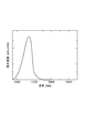
- FIG. 3 shows an emission spectrum of the silicon light emitting device 1 when a 40 mA measurement current is injected into the silicon light emitting device 1 having the insulating film 11 having a thickness of 2 nm at room temperature.
- the horizontal axis of FIG. 3 represents the wavelength (nm) of light emitted from the silicon light emitting element 1.
- the vertical axis in FIG. 3 represents the light emission intensity (arb. Unit) of the silicon light emitting device 1.
- the emission intensity can be controlled by controlling the current injected into the silicon light emitting device 1, but the spectrum does not change. As shown in FIG.
- FIG. 4 is a diagram illustrating the relationship between the film thickness of the insulating film 11 of the silicon light emitting element 1 and the light emission intensity of the silicon light emitting element 1.
- the horizontal axis in FIG. 4 represents the film thickness (nm) of the insulating film 11.
- the vertical axis of FIG. 4 represents the light emission intensity (arb. Unit) of the silicon light emitting element 1 and is represented by a scale where the light emission intensity of the silicon light emitting element not having the insulating film 11 is 1.
- the data shown in FIG. 4 is data obtained when a 40 mA measurement current is injected into the silicon light emitting device 1 at room temperature. As shown in FIG.
- the light emission intensity of the light emitting element 1 having the insulating film 11 is improved as compared with the light emission intensity of the silicon light emitting element not having the insulating film 11.
- the thickness of the insulating film 11 is about 3 nm
- the light emission intensity of the silicon light emitting element 1 is improved by three orders of magnitude or more compared to the light emission intensity of the silicon light emitting element not having the insulating film 11. This is presumably because carriers generated by currents injected from the first electrode 13 and the second electrode 14 move through the thin insulating film 11 by the tunnel effect and recombine.
- the silicon layer 12 is doped with carriers at a higher concentration than the silicon substrate 10 (the carrier concentration is one digit or more higher), the carriers moving from the silicon layer 12 to the silicon substrate 10 by the tunnel effect It is considered dominant. For this reason, it is considered that carrier recombination is limited to the vicinity of the first surface 10 a of the silicon substrate 10. This is considered a kind of carrier confinement.
- the silicon light emitting device 1 can emit light having a wavelength that easily transmits through the silicon waveguide (light having a wavelength of about 1100 nm or more), as shown in FIG.
- the light emission intensity of the silicon light emitting element 1 is the maximum compared to the light emission intensity of the silicon light emitting element not having the insulating film 11. It has improved more than 3 digits.
- the silicon light emitting element 1 has a low operating voltage of about 1 V, so that stable current injection is possible.
- the results shown in FIGS. 2 to 4 represent the room temperature operation of the silicon light emitting device 1.
- the silicon substrate 10, the insulating film 11, and the silicon layer 12 contain Si.
- the silicon light-emitting element 1 is made of a silicon-based material or a silicon process compatible material, emits light having a wavelength easily transmitted through the silicon waveguide with high intensity, and can stably inject current. Therefore, it is suitable for a silicon photonics light source.
- the carrier concentration of the silicon substrate 10 and the silicon layer 12 is not limited to the above case.
- the carrier concentration of the silicon layer 12 is 5 ⁇ 10 15 cm ⁇ 3 to 5 ⁇ 10 18 cm ⁇ 3
- the carrier concentration of the silicon substrate 10 is 1 ⁇ 10 17 cm ⁇ 3 to 5 ⁇ 10 19 cm ⁇ 3.
- the carrier concentration of the silicon substrate 10 can be higher by one digit or more than the carrier concentration of the silicon layer 12.
- the carrier recombination is considered to be limited to the vicinity of the bonding surface of the silicon layer 12 with the insulating film 11. .
- a plurality of light emitting elements using silicon are known.
- a light emitting element for example, a light emitting element using a Si-based semiconductor having a SiGe superlattice is known. This light emitting element emits infrared light by direct transition.
- the SiGe superlattice requires a precise growth technique, the light emitting device is not easy to manufacture.
- the silicon light emitting device 1 according to this embodiment can be manufactured relatively easily because the device structure is not complicated as shown in FIG.
- a light-emitting element in which Si is doped with Er is also known. This light emitting element emits light having a wavelength of about 1.5 ⁇ m. However, this light emitting device has extremely weak emission intensity at room temperature.
- FIG. 5 is a diagram schematically illustrating the configuration of the silicon light emitting element 2 according to the second embodiment.
- the silicon light emitting element 2 includes a silicon substrate 20, a first silicon layer 21, a first electrode 22, an insulating film 23, a second silicon layer 24, and a second electrode 25. Yes.
- the silicon substrate 20 has a first surface 20a.
- the first silicon layer 21 has n-type conductivity (first conductivity type).
- the first silicon layer 21 is provided on the first surface 20 a of the silicon substrate 20.
- the first silicon layer 21 is bonded to the silicon substrate 20. Furthermore, the first silicon layer 21 has a first region 21 a, a second region 21 b, and a third region 21 c that are sequentially arranged along the first surface 20 a of the silicon substrate 20. The thickness of the first region 21a and the thickness of the third region 21c are substantially the same, but the second region 21b is thicker than the first region 21a and the third region 21c. Therefore, the 2nd field 21b protrudes from the surface of the 1st field 21a and the 3rd field 21c. As described above, a step is provided on the surface of the first silicon layer 21. The first electrode 22 is provided on each of the first region 21 a and the third region 21 c of the first silicon layer 21.
- the first electrode 22 is bonded to the first silicon layer 21.
- the insulating film 23 is provided on the second region 21 b of the first silicon layer 21.
- the insulating film 23 is bonded to the first silicon layer 21.
- the insulating film 23 can be a silicon oxide film or a silicon nitride film, but may be another material containing silicon.
- the second silicon layer 24 has a p-type conductivity type (second conductivity type).
- the second silicon layer 24 is provided on the insulating film 23. Further, the second silicon layer 24 is bonded to the insulating film 23.
- the second electrode 25 is provided on the second silicon layer 24.
- the second electrode 25 is bonded to the second silicon layer 24.
- the insulating film 23 is sandwiched between the first silicon layer 21 and the second silicon layer 24.
- the carrier concentration of the first silicon layer 21 is 5 ⁇ 10 15 cm ⁇ 3 to 5 ⁇ 10 18 cm ⁇ 3 , and the resistivity is about 1 ⁇ ⁇ cm to 0.01 ⁇ ⁇ cm.
- the carrier concentration of the second silicon layer 24 is 1 ⁇ 10 17 cm ⁇ 3 to 5 ⁇ 10 19 cm ⁇ 3 , and the resistivity is about 0.2 ⁇ ⁇ cm to 0.002 ⁇ ⁇ cm.
- the carrier concentration of the second silicon layer 24 is one digit or more higher than the carrier concentration of the first silicon layer 21.
- the thickness of the second silicon layer 24 is 0.1 ⁇ m to 2 ⁇ m.
- the film thickness of the insulating film 23 is 0.3 nm to 11 nm.
- a method for manufacturing the silicon light emitting element 2 will be described.
- a silicon substrate 20 is prepared, and a first silicon layer is formed on the silicon substrate 20 by epitaxial growth.
- the surface of the first silicon layer is thermally oxidized to provide an insulating film (silicon oxide film) on the surface of the first silicon layer.
- the method of providing the insulating film may be chemical oxidation.
- the oxidation temperature, the oxidation time, etc. of thermal oxidation are adjusted so that the film thickness of the insulating film is about 0.3 nm to 11 nm.
- a second silicon layer having a thickness of 0.1 ⁇ m to 2 ⁇ m is formed on the insulating film by epitaxial growth.
- the first silicon layer is doped with n-type carriers so that the carrier concentration becomes 5 ⁇ 10 15 cm ⁇ 3 to 5 ⁇ 10 18 cm ⁇ 3, and the second silicon layer has a carrier concentration.
- the p-type carrier is doped so that becomes 1 ⁇ 10 17 cm ⁇ 3 to 5 ⁇ 10 19 cm ⁇ 3 .
- the amount of each doping is adjusted so that the carrier concentration of the second silicon layer is higher by one digit or more than the carrier concentration of the first silicon layer.
- the insulating film and the second silicon layer thus provided are removed by etching leaving the central portion (the edges of the insulating film and the second silicon layer are removed by etching), and the first A part (edge) of the silicon layer is exposed.
- a portion of the exposed first silicon layer is further etched to provide a step on the surface of the first silicon layer.
- a first silicon layer 21, an insulating film 23, and a second silicon layer 24 are formed on the silicon substrate 20.
- the first electrode 22 is deposited on the first region 21a and the third region 21c of the first silicon layer 21 exposed by the above etching.
- a second electrode 25 is provided on the second silicon layer 24 by vapor deposition.
- the silicon light emitting element 2 according to the second embodiment described above can control the carrier concentration in the first silicon layer 21 with high accuracy and has high applicability.
- the carrier concentration of the first silicon layer 21 and the second silicon layer 24 is not limited to the above case.
- the carrier concentration of the second silicon layer 24 is 5 ⁇ 10 15 cm ⁇ 3 to 5 ⁇ 10 18 cm ⁇ 3
- the carrier concentration of the first silicon layer 21 is 1 ⁇ 10 17 cm ⁇ 3 to
- the carrier concentration of the first silicon layer 21 may be 5 ⁇ 10 19 cm ⁇ 3 or more than the carrier concentration of the second silicon layer 24.
- FIG. 6 is a diagram schematically illustrating the configuration of the silicon light emitting element 3 according to the third embodiment.
- the silicon light emitting element 3 includes a first silicon layer 26 in place of the first silicon layer 21 of the silicon light emitting element 2.
- Other configurations of the silicon light emitting element 3 are the same as those of the silicon light emitting element 2.
- the first silicon layer 26 is provided on the first surface 20 a of the silicon substrate 20.
- the first silicon layer 26 includes a first region 26 a, a second region 26 b, and a third region 26 c that are sequentially arranged along the first surface 20 a of the silicon substrate 20.
- the thicknesses of the first region 26a, the second region 26b, and the third region 26c are substantially the same. Therefore, no step is provided on the surface of the first silicon layer 26.
- An insulating film 23, a second silicon layer 24, and a second electrode 25 are sequentially provided on the second region 26b.
- the carrier concentration of the first silicon layer 26 is 5 ⁇ 10 15 cm ⁇ 3 to 5 ⁇ 10 18 cm ⁇ 3 , and the resistivity is about 1 ⁇ ⁇ cm to 0.01 ⁇ ⁇ cm.
- the carrier concentration of the second silicon layer 24 is 1 ⁇ 10 17 cm ⁇ 3 to 5 ⁇ 10 19 cm ⁇ 3 , and the resistivity is about 0.2 ⁇ ⁇ cm to 0.002 ⁇ ⁇ cm.
- the carrier concentration of the second silicon layer 24 is one digit or more higher than the carrier concentration of the first silicon layer 26.
- the silicon light emitting device 3 according to the third embodiment can control the carrier concentration in the first silicon layer 26 with high accuracy, and has high applicability.
- the carrier concentration of the first silicon layer 26 and the second silicon layer 24 is not limited to the above case.
- the carrier concentration of the second silicon layer 24 is 5 ⁇ 10 15 cm ⁇ 3 to 5 ⁇ 10 18 cm ⁇ 3
- the carrier concentration of the first silicon layer 26 is 1 ⁇ 10 17 cm ⁇ 3 to
- the carrier concentration of the first silicon layer 26 may be 5 ⁇ 10 19 cm ⁇ 3 or more than the carrier concentration of the second silicon layer 24.
- a silicon substrate of a first conductivity type having a first surface and a second surface opposite to the first surface, and a first of the silicon substrate.
- An insulating film provided on the surface, a second conductive type silicon layer different from the first conductive type provided on the insulating film, a first electrode provided on the silicon layer, and a second electrode of the silicon substrate.
- the structure is 10 17 cm ⁇ 3 to 5 ⁇ 10 19 cm ⁇ 3 , more than an order of magnitude higher than the carrier concentration of the silicon substrate, and the insulating film has a thickness of 0.3 nm to 5 nm.
- a first conductivity type silicon substrate having a first surface and a second surface opposite to the first surface, and a first of the silicon substrate.
- An insulating film provided on the surface; a silicon layer of a second conductivity type different from the first conductivity type provided on the insulating film; a first electrode provided on the silicon layer; and a second electrode of the silicon substrate.
- the structure is 17 cm ⁇ 3 to 5 ⁇ 10 19 cm ⁇ 3 , more than an order of magnitude higher than the carrier concentration of the silicon layer, and the insulating film has a thickness of 0.3 nm to 5 nm.
- the silicon substrate having the first surface and the first surface of the silicon substrate are provided and sequentially disposed along the first surface.
- a first silicon layer of a first conductivity type having a first region, a second region, and a third region; a first electrode provided on each of the first region and the third region of the first silicon layer;
- An insulating film provided on the second region of the first silicon layer, a second silicon layer of a second conductivity type different from the first conductivity type provided on the insulating film, and provided on the second silicon layer
- the carrier concentration of the first silicon layer is 5 ⁇ 10 15 cm ⁇ 3 to 5 ⁇ 10 18 cm ⁇ 3
- the carrier concentration of the second silicon layer is 1 a ⁇ 10 17 cm -3 ⁇ 5 ⁇ 10 19 cm -3
- the thickness of the insulating film uses a configuration which is 0.3 nm ⁇ 5 nm.
- the silicon substrate having the first surface and the first surface of the silicon substrate are provided and sequentially disposed along the first surface.
- a first silicon layer of a first conductivity type having a first region, a second region, and a third region; a first electrode provided on each of the first region and the third region of the first silicon layer;
- An insulating film provided on the second region of the first silicon layer, a second silicon layer of a second conductivity type different from the first conductivity type provided on the insulating film, and provided on the second silicon layer
- the second silicon layer has a carrier concentration of 5 ⁇ 10 15 cm ⁇ 3 to 5 ⁇ 10 18 cm ⁇ 3
- the first silicon layer has a carrier concentration of 1 a ⁇ 10 17 cm -3 ⁇ 5 ⁇ 10 19 cm -3
- the carrier concentration of the second silicon layer More than an order of magnitude larger, the thickness of the insulating film uses a configuration which is 0.3 nm ⁇ 5 nm.
- the material of the insulating film preferably includes silicon, and more specifically, the insulating film is preferably a silicon oxide film or a silicon nitride film. .
- the present invention can emit light having a wavelength easily transmitted through a silicon waveguide with high intensity, and can therefore be used as a light source for silicon photonics.
- Silicon light emitting element 10 20... Silicon substrate, 10 a, 20 a... First surface, 10 b... Second surface, 11, 23. 1 electrode, 14, 25 ... second electrode, 21, 26 ... first silicon layer, 24 ... second silicon layer, 21a, 26a ... first region, 21b, 26b ... second region, 21c, 26c ... Third region.
Landscapes
- Led Devices (AREA)
- Semiconductor Lasers (AREA)
Abstract
第1の面10aと該第1の面10aの反対側にある第2の面10bとを有する第1導電型のシリコン基板10と、シリコン基板10の第1の面10a上に設けられた絶縁膜11と、絶縁膜11上に設けられ第1導電型と異なる第2導電型のシリコン層12と、シリコン層12上に設けられた第1の電極13と、シリコン基板の第2の面上に設けられた第2の電極14と、を備え、シリコン基板10のキャリア濃度は、5×1015cm-3~5×1018cm-3であり、シリコン層12のキャリア濃度は、1×1017cm-3~5×1019cm-3であり、且つ、シリコン基板10のキャリア濃度より一桁以上大きく、絶縁膜11の膜厚は、0.3nm~5nmである。これにより、シリコンフォトニクスの光源に適用可能なシリコン発光素子が実現される。
Description
本発明は、シリコン発光素子に関する。
近年、シリコンフォトニクスが注目を集めている。シリコンフォトニクスは、シリコンを用いた発光素子やシリコン導波路等を、LSI内のチップ間又はチップ内に集積することによって、消費電力の低減や、信号処理速度の向上を図るための技術である。このシリコンフォトニクスの光源に、安価で環境負荷の小さいシリコンを用いた発光素子が望まれている。また、シリコンのバンドギャップ(室温で約1.125eV)より低いエネルギーの光(約1100nm以上の波長の光)がシリコン導波路を透過し易いので、このような光を発する発光素子が要求されている。シリコンを用いた発光素子の一例が特許文献1及び特許文献2に記載されている。特許文献1及び特許文献2に記載のシリコン発光ダイオードは、何れもSOI基板上に厚さ10nm以下のpn接合部を有している。これらの特許文献1及び特許文献2に記載のシリコン発光ダイオードは、シリコンのバンドギャップより高いエネルギーの光(波長約770nm~1000nm)を発する。これは、pn接合部を薄くすることによって発現する量子閉じ込め効果の影響だと考えられている。
しかしながら、波長770nm~1000nmの光はシリコン導波路を透過し難い。したがって、特許文献1及び特許文献2に記載のシリコン発光ダイオードを、シリコンフォトニクスの光源に適用することは困難である。また、シリコンを用いた他の発光素子として、ポーラスSiやSi/SiO2ナノ構造を有するシリコン発光素子が知られている。しかし、ポーラスSiやSi/SiO2ナノ構造を有するシリコン発光素子の発する光は可視光であり、やはりシリコン導波路を透過し難い。したがって、ポーラスSiやSi/SiO2ナノ構造を有するシリコン発光素子は、シリコンフォトニクスの光源に適用することは困難である。そこで、本発明は、シリコンフォトニクスの光源に適用可能なシリコン発光素子を提供することを課題とする。
本発明のシリコン発光素子は、第1の面と該第1の面の反対側にある第2の面とを有する第1導電型のシリコン基板と、シリコン基板の第1の面上に設けられた絶縁膜と、絶縁膜上に設けられ第1導電型と異なる第2導電型のシリコン層と、シリコン層上に設けられた第1の電極と、シリコン基板の第2の面上に設けられた第2の電極と、を備え、シリコン基板のキャリア濃度は、5×1015cm-3~5×1018cm-3であり、シリコン層のキャリア濃度は、1×1017cm-3~5×1019cm-3であり、且つ、シリコン基板のキャリア濃度より一桁以上大きく、絶縁膜の膜厚は、0.3nm~5nmである、ことを特徴とする。
また、本発明のシリコン発光素子は、第1の面と該第1の面の反対側にある第2の面とを有する第1導電型のシリコン基板と、シリコン基板の第1の面上に設けられた絶縁膜と、絶縁膜上に設けられ第1導電型と異なる第2導電型のシリコン層と、シリコン層上に設けられた第1の電極と、シリコン基板の第2の面上に設けられた第2の電極と、を備え、シリコン層のキャリア濃度は、5×1015cm-3~5×1018cm-3であり、シリコン基板のキャリア濃度は、1×1017cm-3~5×1019cm-3であり、且つ、シリコン層のキャリア濃度より一桁以上大きく、絶縁膜の膜厚は、0.3nm~5nmである、ことを特徴とする。
また、本発明のシリコン発光素子は、第1の面を有するシリコン基板と、シリコン基板の第1の面上に設けられ、該第1の面に沿って順に配置された第1領域、第2領域及び第3領域を有する第1導電型の第1のシリコン層と、第1のシリコン層の第1領域及び第3領域上にそれぞれ設けられた第1の電極と、第1のシリコン層の第2領域上に設けられた絶縁膜と、絶縁膜上に設けられ第1導電型と異なる第2導電型の第2のシリコン層と、第2のシリコン層上に設けられた第2の電極と、を備え、第1のシリコン層のキャリア濃度は、5×1015cm-3~5×1018cm-3であり、第2のシリコン層のキャリア濃度は、1×1017cm-3~5×1019cm-3であり、且つ、第1のシリコン層のキャリア濃度より一桁以上大きく、絶縁膜の膜厚は、0.3nm~5nmである、ことを特徴とする。
また、本発明のシリコン発光素子は、第1の面を有するシリコン基板と、シリコン基板の第1の面上に設けられ、該第1の面に沿って順に配置された第1領域、第2領域及び第3領域を有する第1導電型の第1のシリコン層と、第1のシリコン層の第1領域及び第3領域上にそれぞれ設けられた第1の電極と、第1のシリコン層の第2領域上に設けられた絶縁膜と、絶縁膜上に設けられ第1導電型と異なる第2導電型の第2のシリコン層と、第2のシリコン層上に設けられた第2の電極と、を備え、第2のシリコン層のキャリア濃度は、5×1015cm-3~5×1018cm-3であり、第1のシリコン層のキャリア濃度は、1×1017cm-3~5×1019cm-3であり、且つ、第2のシリコン層のキャリア濃度より一桁以上大きく、絶縁膜の膜厚は、0.3nm~5nmである、ことを特徴とする。
本発明者は、シリコン導波路を透過しやすい波長の光を比較的高い強度で発することが要求されるシリコンフォトニクスの光源に適用可能なシリコン発光素子を開発すべく研究を重ねた。この研究の結果、本発明者は、膜厚0.3nm~5nmの絶縁膜を有する本発明のシリコン発光素子が、シリコン導波路を透過しやすい波長の光を高い強度で発することを見出した。
本発明によれば、シリコンフォトニクスの光源に適用可能なシリコン発光素子を提供することができる。
(第1実施形態)以下、図面を参照して、本発明に係るシリコン発光素子の第1実施形態について詳細に説明する。なお、図面の説明において、可能な場合には、同一要素には同一符号を付し、重複する説明を省略する。図1を参照して、第1実施形態に係るシリコン発光素子1の構成を説明する。図1は第1実施形態に係るシリコン発光素子1の構成を模式的に表す図である。シリコン発光素子1は、シリコン基板10と、絶縁膜11と、シリコン層12と、第1の電極13と、第2の電極14と、を備える。シリコン基板10は、第1の面10aと第2の面10bとを有している。また、シリコン基板10は、n型の導電型(第1導電型)を有している。絶縁膜11は、シリコン基板10の第1の面10a上に設けられている。絶縁膜11は、シリコン基板10に接合されている。絶縁膜11は、シリコン酸化膜又はシリコン窒化膜とすることができるがシリコンを含む他の材料であってもよい。シリコン層12は、絶縁膜11上に設けられている。シリコン層12は、絶縁膜11に接合されている。シリコン層12は、p型の導電型(第2導電型)を有している。第1の電極13は、シリコン層12上に設けられている。第1の電極13は、シリコン層12に接合されている。第2の電極14は、シリコン基板10の第2の面10b上に設けられている。第2の電極14は、シリコン基板10に接合されている。絶縁膜11は、シリコン基板10とシリコン層12との間に挟まれている。
シリコン基板10のキャリア濃度は5×1015cm-3~5×1018cm-3であり、抵抗率は、約1Ω・cm~0.01Ω・cmである。また、シリコン層12のキャリア濃度は、1×1017cm-3~5×1019cm-3であり、抵抗率は、約0.2Ω・cm~0.002Ω・cmである。ただし、シリコン層12のキャリア濃度はシリコン基板10のキャリア濃度に比べて一桁以上大きい。シリコン層12の厚さは0.1μm~2μmである。絶縁膜11の膜厚は0.3nm~11nmである。
次にシリコン発光素子1の製造方法について説明する。先ず、シリコン基板10の表面を熱酸化させ、シリコン基板10の表面に絶縁膜11(シリコン酸化膜)を設ける。絶縁膜11を設ける方法は、化学酸化であってもよい。このとき、絶縁膜11の膜厚が約0.3nm~11nmになるように、熱酸化の酸化温度や酸化時間等を調整する。次に、絶縁膜11上に厚さ0.1μm~2μmのシリコン層12を成長させる。そして、第1の電極13及び第2の電極14を、それぞれシリコン層12及びシリコン基板10上に蒸着して設ける。ここで、シリコン基板10には、キャリア濃度が5×1015cm-3~5×1018cm-3となるようにn型キャリアをドープし、シリコン層12には、キャリア濃度が1×1017cm-3~5×1019cm-3となるようにp型キャリアをドープする。ただし、シリコン層12のキャリア濃度がシリコン基板10のキャリア濃度より一桁以上大きくなるように各ドープ量を調整する。
次に、図2を参照して、シリコン発光素子1のV-I特性(電圧-電流特性)について説明する。図2は、膜厚2nmの絶縁膜11を有するシリコン発光素子1のV-I特性を表している。図2の横軸は、シリコン発光素子1に印可するバイアス電圧(V)を表しており、縦軸はシリコン発光素子1に流れる電流(mA)を表している。図2に示すように、シリコン発光素子1は、良好なp-n接合特性を発揮するので、ダイオードとして動作することがわかる。
続いて、図3及び図4を用いて、シリコン発光素子1のEL(Electro Luminescence)特性について説明する。図3は、膜厚2nmの絶縁膜11を有するシリコン発光素子1に40mAの測定電流を室温で注入した場合のシリコン発光素子1の発光スペクトルを表している。図3の横軸は、シリコン発光素子1から発せられる光の波長(nm)を表している。図3の縦軸は、シリコン発光素子1の発光強度(arb.unit)を表している。シリコン発光素子1に注入する電流を制御することにより発光強度を制御することができるが、スペクトルは変わらない。図3に示すように、シリコン発光素子1は、約1140nmの発光ピークを有する。図4は、シリコン発光素子1の絶縁膜11の膜厚と、シリコン発光素子1の発光強度との関係を表す図である。図4の横軸は、絶縁膜11の膜厚(nm)を表している。図4の縦軸は、シリコン発光素子1の発光強度(arb.unit)を表しており、絶縁膜11を有さないシリコン発光素子の発光強度を1とするスケールによって表されている。図4に示すデータは、シリコン発光素子1に40mAの測定電流を室温で注入した際に得られたデータである。図4に示すように、絶縁膜11を有する発光素子1の発光強度は、絶縁膜11を有さないシリコン発光素子の発光強度に比べて向上していることがわかる。特に、絶縁膜11の膜厚が約3nmの場合、シリコン発光素子1の発光強度は、絶縁膜11を有さないシリコン発光素子の発光強度に比べて3桁以上も向上している。これは、第1の電極13及び第2の電極14から注入される電流により発生するキャリアが、薄い絶縁膜11をトンネル効果により移動し、再結合するためであると考えられる。なお、シリコン層12がシリコン基板10より高濃度でキャリアがドープされているため(キャリア濃度が一桁以上大きい)、シリコン層12からシリコン基板10へトンネル効果により移動するキャリアが、全体のキャリアの中で支配的であると考えられる。このため、キャリアの再結合は、シリコン基板10の第1の面10a近傍に限定されると考えられる。これは、一種のキャリア閉じ込めであると考えられる。
以上説明したように、本実施形態に係るシリコン発光素子1は、図3に示すように、シリコン導波路を透過し易い波長の光(波長約1100nm以上の光)を発することができる。また、図4に示すように、絶縁膜11の膜厚が0.3nm~5nmの場合、シリコン発光素子1の発光強度は、絶縁膜11を有さないシリコン発光素子の発光強度に比べて最大で3桁以上も向上している。また、図2に示すように、シリコン発光素子1は、動作電圧が約1Vと低いので安定な電流注入が可能である。また、図2~図4に示す結果は、シリコン発光素子1の室温動作を表している。また、シリコン基板10、絶縁膜11及びシリコン層12はSiを含んでいる。このように、シリコン発光素子1は、シリコン系材料又はシリコンプロセス適合材料で構成されており、シリコン導波路を透過しやすい波長の光を高い強度で発し、安定した電流注入が可能であり、室温で用いることができるのでシリコンフォトニクスの光源に適している。
なお、シリコン基板10及びシリコン層12のキャリア濃度は、上記の場合に限らない。例えば、シリコン層12のキャリア濃度は5×1015cm-3~5×1018cm-3であり、シリコン基板10のキャリア濃度は、1×1017cm-3~5×1019cm-3であり、且つ、シリコン基板10のキャリア濃度は、シリコン層12のキャリア濃度に比べて一桁以上大きい、とすることができる。このように、シリコン基板10がシリコン層12より高濃度でキャリアがドープされている場合においては、キャリアの再結合は、シリコン層12の絶縁膜11との接合面近傍に限定されると考えられる。
なお、シリコン発光素子1以外にもシリコンを用いた複数の発光素子が知られている。このような発光素子としては、例えば、SiGe超格子を有するSi系半導体を用いた発光素子が知られている。この発光素子は、直接遷移により赤外光を発する。しかし、SiGe超格子は精密な成長技術が要求されるので、この発光素子は製造が容易でない。これに対し、本実施形態に係るシリコン発光素子1は、図1に示すように、素子構造が複雑でないので比較的容易に製造できる。また、SiにErをドープした発光素子も知られている。この発光素子は約1.5μmの波長の光を発する。しかし、この発光素子は室温における発光強度が極めて弱い。
(第2実施形態)続いて、本発明に係るシリコン発光素子の第2実施形態について詳細に説明する。図5を参照して、第2実施形態に係るシリコン発光素子2の構成を説明する。図5は、第2実施形態に係るシリコン発光素子2の構成を模式的に表す図である。シリコン発光素子2は、シリコン基板20と、第1のシリコン層21と、第1の電極22と、絶縁膜23と、第2のシリコン層24と、第2の電極25と、を有している。シリコン基板20は、第1の面20aを有している。第1のシリコン層21は、n型の導電型(第1導電型)を有している。第1のシリコン層21は、シリコン基板20の第1の面20a上に設けられている。また、第1のシリコン層21は、シリコン基板20に接合されている。さらに、第1のシリコン層21は、シリコン基板20の第1の面20aに沿って順に配置された第1領域21a、第2領域21b及び第3領域21cを有する。第1領域21aの厚さと第3領域21cの厚さとは略同一であるが、第2領域21bは、第1領域21a及び第3領域21cよりも厚い。したがって、第2領域21bは、第1領域21a及び第3領域21cの表面より突出している。このように、第1のシリコン層21の表面には段差が設けられている。第1の電極22は、第1のシリコン層21の第1領域21a及び第3領域21c上にそれぞれ設けられている。第1の電極22は、第1のシリコン層21に接合されている。絶縁膜23は、第1のシリコン層21の第2領域21b上に設けられている。絶縁膜23は、第1のシリコン層21に接合されている。絶縁膜23は、シリコン酸化膜又はシリコン窒化膜とすることができるがシリコンを含む他の材料であってもよい。第2のシリコン層24はp型の導電型(第2導電型)を有している。第2のシリコン層24は、絶縁膜23上に設けられている。また、第2のシリコン層24は、絶縁膜23に接合されている。第2の電極25は、第2のシリコン層24上に設けられている。第2の電極25は、第2のシリコン層24に接合されている。絶縁膜23は、第1のシリコン層21と第2のシリコン層24との間に挟まれている。
第1のシリコン層21のキャリア濃度は5×1015cm-3~5×1018cm-3であり、抵抗率は、約1Ω・cm~0.01Ω・cmである。また、第2のシリコン層24のキャリア濃度は、1×1017cm-3~5×1019cm-3であり、抵抗率は、約0.2Ω・cm~0.002Ω・cmである。ただし、第2のシリコン層24のキャリア濃度は第1のシリコン層21のキャリア濃度に比べて一桁以上大きい。第2のシリコン層24の厚さは0.1μm~2μmである。絶縁膜23の膜厚は0.3nm~11nmである。
次にシリコン発光素子2の製造方法について説明する。先ず、シリコン基板20を用意し、このシリコン基板20上に第1のシリコン層をエピタキシャル成長によって形成する。次に第1のシリコン層の表面を熱酸化させ、第1のシリコン層の表面に絶縁膜(シリコン酸化膜)を設ける。絶縁膜を設ける方法は、化学酸化であってもよい。このとき、絶縁膜の膜厚が約0.3nm~11nmになるように、熱酸化の酸化温度や酸化時間等を調整する。次に、絶縁膜上に厚さ0.1μm~2μmの第2のシリコン層をエピタキシャル成長によって形成する。ここで、第1のシリコン層には、キャリア濃度が5×1015cm-3~5×1018cm-3となるようにn型キャリアをドープし、第2のシリコン層には、キャリア濃度が1×1017cm-3~5×1019cm-3となるようにp型キャリアをドープする。ただし、第2のシリコン層のキャリア濃度が第1のシリコン層のキャリア濃度より一桁以上大きくなるように各ドープ量を調整する。そして、このように設けられた絶縁膜及び第2のシリコン層を、中央部分を残してエッチングして除去し(絶縁膜及び第2のシリコン層の縁部をエッチングして除去し)、第1のシリコン層の一部(縁部)を露出させる。この露出した第1のシリコン層の一部をさらにエッチングし、第1のシリコン層の表面に段差を設ける。このエッチングによって、シリコン基板20上に、第1のシリコン層21、絶縁膜23及び第2のシリコン層24が形成される。この後、上記のエッチングによって露出した第1のシリコン層21の第1領域21a及び第3領域21c上に第1の電極22を蒸着して設ける。さらに、第2のシリコン層24上に、第2の電極25を蒸着して設ける。以上説明した、第2実施形態に係るシリコン発光素子2は、第1のシリコン層21内におけるキャリア濃度を精度良く制御可能であり、高い応用性がある。
なお、第1のシリコン層21及び第2のシリコン層24のキャリア濃度は、上記の場合に限らない。例えば、第2のシリコン層24のキャリア濃度は、5×1015cm-3~5×1018cm-3であり、第1のシリコン層21のキャリア濃度は、1×1017cm-3~5×1019cm-3であり、且つ、第1のシリコン層21のキャリア濃度は、第2のシリコン層24のキャリア濃度より一桁以上大きい、とすることができる。
(第3実施形態)次に、図6を参照して、本発明のシリコン発光素子の第3実施形態について説明する。図6は、第3実施形態に係るシリコン発光素子3の構成を模式的に表す図ある。シリコン発光素子3は、シリコン発光素子2の第1のシリコン層21に替えて第1のシリコン層26を有する。シリコン発光素子3の他の構成は、シリコン発光素子2と同様である。第1のシリコン層26は、シリコン基板20の第1の面20a上に設けられている。第1のシリコン層26は、シリコン基板20の第1の面20aに沿って順に配置された第1領域26a、第2領域26b及び第3領域26cを有する。第1領域26a、第2領域26b及び第3領域26cの厚さは、略同一である。したがって、第1のシリコン層26の表面には、段差が設けられていない。第2領域26b上に絶縁膜23、第2のシリコン層24及び第2の電極25が順に設けられている。第1のシリコン層26のキャリア濃度は、5×1015cm-3~5×1018cm-3であり、抵抗率は、約1Ω・cm~0.01Ω・cmである。また、第2のシリコン層24のキャリア濃度は、1×1017cm-3~5×1019cm-3であり、抵抗率は、約0.2Ω・cm~0.002Ω・cmである。ただし、第2のシリコン層24のキャリア濃度は第1のシリコン層26のキャリア濃度に比べて一桁以上大きい。以上説明した、第3実施形態に係るシリコン発光素子3は、第1のシリコン層26内におけるキャリア濃度を精度良く制御可能であり、高い応用性がある。
なお、第1のシリコン層26及び第2のシリコン層24のキャリア濃度は、上記の場合に限定されない。例えば、第2のシリコン層24のキャリア濃度は、5×1015cm-3~5×1018cm-3であり、第1のシリコン層26のキャリア濃度は、1×1017cm-3~5×1019cm-3であり、且つ、第1のシリコン層26のキャリア濃度は、第2のシリコン層24のキャリア濃度より一桁以上大きい、とすることができる。
ここで、上記第1実施形態によるシリコン発光素子では、第1の面と該第1の面の反対側にある第2の面とを有する第1導電型のシリコン基板と、シリコン基板の第1の面上に設けられた絶縁膜と、絶縁膜上に設けられ第1導電型と異なる第2導電型のシリコン層と、シリコン層上に設けられた第1の電極と、シリコン基板の第2の面上に設けられた第2の電極と、を備え、シリコン基板のキャリア濃度は、5×1015cm-3~5×1018cm-3であり、シリコン層のキャリア濃度は、1×1017cm-3~5×1019cm-3であり、且つ、シリコン基板のキャリア濃度より一桁以上大きく、絶縁膜の膜厚は、0.3nm~5nmである構成を用いている。
或いは、上記第1実施形態によるシリコン発光素子では、第1の面と該第1の面の反対側にある第2の面とを有する第1導電型のシリコン基板と、シリコン基板の第1の面上に設けられた絶縁膜と、絶縁膜上に設けられ第1導電型と異なる第2導電型のシリコン層と、シリコン層上に設けられた第1の電極と、シリコン基板の第2の面上に設けられた第2の電極と、を備え、シリコン層のキャリア濃度は、5×1015cm-3~5×1018cm-3であり、シリコン基板のキャリア濃度は、1×1017cm-3~5×1019cm-3であり、且つ、シリコン層のキャリア濃度より一桁以上大きく、絶縁膜の膜厚は、0.3nm~5nmである構成を用いている。
また、上記第2及び第3実施形態によるシリコン発光素子では、第1の面を有するシリコン基板と、シリコン基板の第1の面上に設けられ、該第1の面に沿って順に配置された第1領域、第2領域及び第3領域を有する第1導電型の第1のシリコン層と、第1のシリコン層の第1領域及び第3領域上にそれぞれ設けられた第1の電極と、第1のシリコン層の第2領域上に設けられた絶縁膜と、絶縁膜上に設けられ第1導電型と異なる第2導電型の第2のシリコン層と、第2のシリコン層上に設けられた第2の電極と、を備え、第1のシリコン層のキャリア濃度は、5×1015cm-3~5×1018cm-3であり、第2のシリコン層のキャリア濃度は、1×1017cm-3~5×1019cm-3であり、且つ、第1のシリコン層のキャリア濃度より一桁以上大きく、絶縁膜の膜厚は、0.3nm~5nmである構成を用いている。
或いは、上記第2及び第3実施形態によるシリコン発光素子では、第1の面を有するシリコン基板と、シリコン基板の第1の面上に設けられ、該第1の面に沿って順に配置された第1領域、第2領域及び第3領域を有する第1導電型の第1のシリコン層と、第1のシリコン層の第1領域及び第3領域上にそれぞれ設けられた第1の電極と、第1のシリコン層の第2領域上に設けられた絶縁膜と、絶縁膜上に設けられ第1導電型と異なる第2導電型の第2のシリコン層と、第2のシリコン層上に設けられた第2の電極と、を備え、第2のシリコン層のキャリア濃度は、5×1015cm-3~5×1018cm-3であり、第1のシリコン層のキャリア濃度は、1×1017cm-3~5×1019cm-3であり、且つ、第2のシリコン層のキャリア濃度より一桁以上大きく、絶縁膜の膜厚は、0.3nm~5nmである構成を用いている。
このような第1~第3実施形態によるシリコン発光素子においては、絶縁膜の材料はシリコンを含むことが好ましく、より具体的には、絶縁膜はシリコン酸化膜又はシリコン窒化膜であることが好ましい。
本発明は、シリコン導波路を透過しやすい波長の光を高い強度で発することが可能であり、したがって、シリコンフォトニクスの光源として利用可能である。
1,2,3…シリコン発光素子、10,20…シリコン基板、10a,20a…第1の面、10b…第2の面、11,23…絶縁膜、12…シリコン層、13,22…第1の電極、14,25…第2の電極、21,26…第1のシリコン層、24…第2のシリコン層、21a,26a…第1領域、21b,26b…第2領域、21c,26c…第3領域。
Claims (6)
- 第1の面と該第1の面の反対側にある第2の面とを有する第1導電型のシリコン基板と、
前記シリコン基板の前記第1の面上に設けられた絶縁膜と、
前記絶縁膜上に設けられ前記第1導電型と異なる第2導電型のシリコン層と、
前記シリコン層上に設けられた第1の電極と、
前記シリコン基板の前記第2の面上に設けられた第2の電極と、を備え、
前記シリコン基板のキャリア濃度は、5×1015cm-3~5×1018cm-3であり、
前記シリコン層のキャリア濃度は、1×1017cm-3~5×1019cm-3であり、且つ、前記シリコン基板のキャリア濃度より一桁以上大きく、
前記絶縁膜の膜厚は、0.3nm~5nmである、
ことを特徴とするシリコン発光素子。 - 第1の面と該第1の面の反対側にある第2の面とを有する第1導電型のシリコン基板と、
前記シリコン基板の前記第1の面上に設けられた絶縁膜と、
前記絶縁膜上に設けられ前記第1導電型と異なる第2導電型のシリコン層と、
前記シリコン層上に設けられた第1の電極と、
前記シリコン基板の前記第2の面上に設けられた第2の電極と、を備え、
前記シリコン層のキャリア濃度は、5×1015cm-3~5×1018cm-3であり、
前記シリコン基板のキャリア濃度は、1×1017cm-3~5×1019cm-3であり、且つ、前記シリコン層のキャリア濃度より一桁以上大きく、
前記絶縁膜の膜厚は、0.3nm~5nmである、
ことを特徴とするシリコン発光素子。 - 第1の面を有するシリコン基板と、
前記シリコン基板の第1の面上に設けられ、該第1の面に沿って順に配置された第1領域、第2領域及び第3領域を有する第1導電型の第1のシリコン層と、
前記第1のシリコン層の前記第1領域及び前記第3領域上にそれぞれ設けられた第1の電極と、
前記第1のシリコン層の前記第2領域上に設けられた絶縁膜と、
前記絶縁膜上に設けられ前記第1導電型と異なる第2導電型の第2のシリコン層と、
前記第2のシリコン層上に設けられた第2の電極と、
を備え、
前記第1のシリコン層のキャリア濃度は、5×1015cm-3~5×1018cm-3であり、
前記第2のシリコン層のキャリア濃度は、1×1017cm-3~5×1019cm-3であり、且つ、前記第1のシリコン層のキャリア濃度より一桁以上大きく、
前記絶縁膜の膜厚は、0.3nm~5nmである、
ことを特徴とするシリコン発光素子。 - 第1の面を有するシリコン基板と、
前記シリコン基板の第1の面上に設けられ、該第1の面に沿って順に配置された第1領域、第2領域及び第3領域を有する第1導電型の第1のシリコン層と、
前記第1のシリコン層の前記第1領域及び前記第3領域上にそれぞれ設けられた第1の電極と、
前記第1のシリコン層の前記第2領域上に設けられた絶縁膜と、
前記絶縁膜上に設けられ前記第1導電型と異なる第2導電型の第2のシリコン層と、
前記第2のシリコン層上に設けられた第2の電極と、
を備え、
前記第2のシリコン層のキャリア濃度は、5×1015cm-3~5×1018cm-3であり、
前記第1のシリコン層のキャリア濃度は、1×1017cm-3~5×1019cm-3であり、且つ、前記第2のシリコン層のキャリア濃度より一桁以上大きく、
前記絶縁膜の膜厚は、0.3nm~5nmである、
ことを特徴とするシリコン発光素子。 - 前記絶縁膜の材料は、シリコンを含むことを特徴とする請求項1~請求項4の何れか一項に記載のシリコン発光素子。
- 前記絶縁膜は、シリコン酸化膜又はシリコン窒化膜であることを特徴とする請求項1~請求項4の何れか一項に記載のシリコン発光素子。
Priority Applications (2)
| Application Number | Priority Date | Filing Date | Title |
|---|---|---|---|
| CN2009801444331A CN102210029B (zh) | 2008-11-06 | 2009-09-08 | 硅发光元件 |
| US13/100,650 US8284345B2 (en) | 2008-11-06 | 2011-05-04 | Silicon light-emitting element |
Applications Claiming Priority (2)
| Application Number | Priority Date | Filing Date | Title |
|---|---|---|---|
| JP2008285545A JP5249721B2 (ja) | 2008-11-06 | 2008-11-06 | シリコン発光素子 |
| JP2008-285545 | 2008-11-06 |
Related Child Applications (1)
| Application Number | Title | Priority Date | Filing Date |
|---|---|---|---|
| US13/100,650 Continuation-In-Part US8284345B2 (en) | 2008-11-06 | 2011-05-04 | Silicon light-emitting element |
Publications (1)
| Publication Number | Publication Date |
|---|---|
| WO2010052967A1 true WO2010052967A1 (ja) | 2010-05-14 |
Family
ID=42152777
Family Applications (1)
| Application Number | Title | Priority Date | Filing Date |
|---|---|---|---|
| PCT/JP2009/065665 Ceased WO2010052967A1 (ja) | 2008-11-06 | 2009-09-08 | シリコン発光素子 |
Country Status (4)
| Country | Link |
|---|---|
| US (1) | US8284345B2 (ja) |
| JP (1) | JP5249721B2 (ja) |
| CN (1) | CN102210029B (ja) |
| WO (1) | WO2010052967A1 (ja) |
Families Citing this family (3)
| Publication number | Priority date | Publication date | Assignee | Title |
|---|---|---|---|---|
| JP5438052B2 (ja) * | 2011-03-09 | 2014-03-12 | 日本電信電話株式会社 | 半導体発光素子 |
| US8748908B2 (en) | 2012-05-07 | 2014-06-10 | Sufian Abedrabbo | Semiconductor optical emission device |
| JP6114934B2 (ja) * | 2012-08-31 | 2017-04-19 | 国立大学法人愛媛大学 | 半導体量子素子 |
Citations (4)
| Publication number | Priority date | Publication date | Assignee | Title |
|---|---|---|---|---|
| JPS62202573A (ja) * | 1986-02-28 | 1987-09-07 | Fujitsu Ltd | 発光デイバイス |
| JP2000188260A (ja) * | 1998-12-22 | 2000-07-04 | Samsung Electro Mech Co Ltd | 窒化物系化合物半導体素子、窒化物系化合物半導体の結晶成長方法、及び窒化物系化合物半導体素子の製造方法 |
| JP2000273450A (ja) * | 1999-03-23 | 2000-10-03 | Mitsubishi Materials Corp | シリコンと窒素を主成分とする発光材料及びその製造方法並びにこれを用いた発光素子 |
| JP2007329468A (ja) * | 2006-05-10 | 2007-12-20 | Kumamoto Univ | 発光素子およびその製造方法 |
Family Cites Families (5)
| Publication number | Priority date | Publication date | Assignee | Title |
|---|---|---|---|---|
| JPH0846237A (ja) | 1994-07-27 | 1996-02-16 | Nippon Telegr & Teleph Corp <Ntt> | シリコン発光ダイオード |
| US6831304B2 (en) * | 2002-02-25 | 2004-12-14 | Showa Denko Kabushiki Kaisha | P-n junction type boron phosphide-based semiconductor light-emitting device and production method thereof |
| JP4320653B2 (ja) * | 2005-09-30 | 2009-08-26 | 日立電線株式会社 | 半導体発光素子 |
| JP5003013B2 (ja) | 2006-04-25 | 2012-08-15 | 株式会社日立製作所 | シリコン発光ダイオード、シリコン光トランジスタ、シリコンレーザー及びそれらの製造方法。 |
| KR101361129B1 (ko) * | 2007-07-03 | 2014-02-13 | 삼성전자주식회사 | 발광소자 및 그 제조방법 |
-
2008
- 2008-11-06 JP JP2008285545A patent/JP5249721B2/ja not_active Expired - Fee Related
-
2009
- 2009-09-08 CN CN2009801444331A patent/CN102210029B/zh not_active Expired - Fee Related
- 2009-09-08 WO PCT/JP2009/065665 patent/WO2010052967A1/ja not_active Ceased
-
2011
- 2011-05-04 US US13/100,650 patent/US8284345B2/en not_active Expired - Fee Related
Patent Citations (4)
| Publication number | Priority date | Publication date | Assignee | Title |
|---|---|---|---|---|
| JPS62202573A (ja) * | 1986-02-28 | 1987-09-07 | Fujitsu Ltd | 発光デイバイス |
| JP2000188260A (ja) * | 1998-12-22 | 2000-07-04 | Samsung Electro Mech Co Ltd | 窒化物系化合物半導体素子、窒化物系化合物半導体の結晶成長方法、及び窒化物系化合物半導体素子の製造方法 |
| JP2000273450A (ja) * | 1999-03-23 | 2000-10-03 | Mitsubishi Materials Corp | シリコンと窒素を主成分とする発光材料及びその製造方法並びにこれを用いた発光素子 |
| JP2007329468A (ja) * | 2006-05-10 | 2007-12-20 | Kumamoto Univ | 発光素子およびその製造方法 |
Also Published As
| Publication number | Publication date |
|---|---|
| CN102210029B (zh) | 2013-03-20 |
| JP5249721B2 (ja) | 2013-07-31 |
| US20110220956A1 (en) | 2011-09-15 |
| JP2010114262A (ja) | 2010-05-20 |
| CN102210029A (zh) | 2011-10-05 |
| US8284345B2 (en) | 2012-10-09 |
Similar Documents
| Publication | Publication Date | Title |
|---|---|---|
| Cho et al. | High efficiency visible electroluminescence from silicon nanocrystals embedded in silicon nitride using a transparent doping layer | |
| Ryu et al. | Next generation of oxide photonic devices: ZnO-based ultraviolet light emitting diodes | |
| Hu et al. | Piezo-phototronic effect on electroluminescence properties of p-type GaN thin films | |
| Abell et al. | Mid-infrared interband cascade light emitting devices with milliwatt output powers at room temperature | |
| CN102957091B (zh) | 张应变半导体光子发射和检测装置和集成的光子学系统 | |
| WO1999005726A1 (en) | Semiconductor with tunnel hole contact sources | |
| US10727431B2 (en) | Optoelectronic devices based on intrinsic plasmon-exciton polaritons | |
| JPH1056201A (ja) | 基板構造、発光装置、基板構造の製造方法および発光装置の製造方法 | |
| US9431577B2 (en) | Wavelength specific silicon light emitting structure | |
| US8440994B2 (en) | Nanotube array electronic and opto-electronic devices | |
| US7671377B2 (en) | Silicon based light emitting diode | |
| JP5249721B2 (ja) | シリコン発光素子 | |
| US8450127B2 (en) | Light emitting semiconductor diode | |
| US20110168970A1 (en) | Optoelectronic light emitting structure | |
| Kong et al. | Low-threshold ZnO random lasing in a homojunction diode with embedded double heterostructure | |
| Kim | Stacking-enabled Si/GaN tunnel junction light-emitting diodes with improved radiative recombination efficiency: K. Kim | |
| KR100808802B1 (ko) | 희토류 원소가 첨가된 무기 전계 발광 레이저 소자 | |
| JP2007043016A (ja) | 結晶シリコン素子、およびその製造方法 | |
| EP1820222A1 (en) | Silicon-based light emitting diode | |
| TWI437730B (zh) | 發光二極體 | |
| CN109273570B (zh) | 一种基于kbbf族晶体的深紫外二极管器件 | |
| KR100644728B1 (ko) | 아연 산화물을 이용한 실리콘 발광소자 및 그 제조방법 | |
| CN105633227B (zh) | 高速调制发光二极管及其制造方法 | |
| JPH0467689A (ja) | トンネル接合発光素子 | |
| US20020121858A1 (en) | Short wavelength ZnO light emitting device and the manufacturing method thereof |
Legal Events
| Date | Code | Title | Description |
|---|---|---|---|
| WWE | Wipo information: entry into national phase |
Ref document number: 200980144433.1 Country of ref document: CN |
|
| 121 | Ep: the epo has been informed by wipo that ep was designated in this application |
Ref document number: 09824667 Country of ref document: EP Kind code of ref document: A1 |
|
| NENP | Non-entry into the national phase |
Ref country code: DE |
|
| 122 | Ep: pct application non-entry in european phase |
Ref document number: 09824667 Country of ref document: EP Kind code of ref document: A1 |