WO2010050341A1 - 紫外光源装置 - Google Patents
紫外光源装置 Download PDFInfo
- Publication number
- WO2010050341A1 WO2010050341A1 PCT/JP2009/067398 JP2009067398W WO2010050341A1 WO 2010050341 A1 WO2010050341 A1 WO 2010050341A1 JP 2009067398 W JP2009067398 W JP 2009067398W WO 2010050341 A1 WO2010050341 A1 WO 2010050341A1
- Authority
- WO
- WIPO (PCT)
- Prior art keywords
- light
- optical waveguide
- light source
- wavelength
- excitation light
- Prior art date
- Legal status (The legal status is an assumption and is not a legal conclusion. Google has not performed a legal analysis and makes no representation as to the accuracy of the status listed.)
- Ceased
Links
Images




Classifications
-
- H—ELECTRICITY
- H01—ELECTRIC ELEMENTS
- H01S—DEVICES USING THE PROCESS OF LIGHT AMPLIFICATION BY STIMULATED EMISSION OF RADIATION [LASER] TO AMPLIFY OR GENERATE LIGHT; DEVICES USING STIMULATED EMISSION OF ELECTROMAGNETIC RADIATION IN WAVE RANGES OTHER THAN OPTICAL
- H01S3/00—Lasers, i.e. devices using stimulated emission of electromagnetic radiation in the infrared, visible or ultraviolet wave range
- H01S3/05—Construction or shape of optical resonators; Accommodation of active medium therein; Shape of active medium
- H01S3/06—Construction or shape of active medium
- H01S3/063—Waveguide lasers, i.e. whereby the dimensions of the waveguide are of the order of the light wavelength
- H01S3/067—Fibre lasers
- H01S3/06708—Constructional details of the fibre, e.g. compositions, cross-section, shape or tapering
- H01S3/06716—Fibre compositions or doping with active elements
-
- B—PERFORMING OPERATIONS; TRANSPORTING
- B82—NANOTECHNOLOGY
- B82Y—SPECIFIC USES OR APPLICATIONS OF NANOSTRUCTURES; MEASUREMENT OR ANALYSIS OF NANOSTRUCTURES; MANUFACTURE OR TREATMENT OF NANOSTRUCTURES
- B82Y20/00—Nanooptics, e.g. quantum optics or photonic crystals
-
- H—ELECTRICITY
- H01—ELECTRIC ELEMENTS
- H01S—DEVICES USING THE PROCESS OF LIGHT AMPLIFICATION BY STIMULATED EMISSION OF RADIATION [LASER] TO AMPLIFY OR GENERATE LIGHT; DEVICES USING STIMULATED EMISSION OF ELECTROMAGNETIC RADIATION IN WAVE RANGES OTHER THAN OPTICAL
- H01S3/00—Lasers, i.e. devices using stimulated emission of electromagnetic radiation in the infrared, visible or ultraviolet wave range
- H01S3/09—Processes or apparatus for excitation, e.g. pumping
- H01S3/091—Processes or apparatus for excitation, e.g. pumping using optical pumping
- H01S3/094—Processes or apparatus for excitation, e.g. pumping using optical pumping by coherent light
- H01S3/094003—Processes or apparatus for excitation, e.g. pumping using optical pumping by coherent light the pumped medium being a fibre
-
- H—ELECTRICITY
- H01—ELECTRIC ELEMENTS
- H01S—DEVICES USING THE PROCESS OF LIGHT AMPLIFICATION BY STIMULATED EMISSION OF RADIATION [LASER] TO AMPLIFY OR GENERATE LIGHT; DEVICES USING STIMULATED EMISSION OF ELECTROMAGNETIC RADIATION IN WAVE RANGES OTHER THAN OPTICAL
- H01S3/00—Lasers, i.e. devices using stimulated emission of electromagnetic radiation in the infrared, visible or ultraviolet wave range
- H01S3/14—Lasers, i.e. devices using stimulated emission of electromagnetic radiation in the infrared, visible or ultraviolet wave range characterised by the material used as the active medium
- H01S3/16—Solid materials
- H01S3/1601—Solid materials characterised by an active (lasing) ion
- H01S3/1603—Solid materials characterised by an active (lasing) ion rare earth
-
- H—ELECTRICITY
- H01—ELECTRIC ELEMENTS
- H01S—DEVICES USING THE PROCESS OF LIGHT AMPLIFICATION BY STIMULATED EMISSION OF RADIATION [LASER] TO AMPLIFY OR GENERATE LIGHT; DEVICES USING STIMULATED EMISSION OF ELECTROMAGNETIC RADIATION IN WAVE RANGES OTHER THAN OPTICAL
- H01S3/00—Lasers, i.e. devices using stimulated emission of electromagnetic radiation in the infrared, visible or ultraviolet wave range
- H01S3/14—Lasers, i.e. devices using stimulated emission of electromagnetic radiation in the infrared, visible or ultraviolet wave range characterised by the material used as the active medium
- H01S3/16—Solid materials
- H01S3/17—Solid materials amorphous, e.g. glass
- H01S3/173—Solid materials amorphous, e.g. glass fluoride glass, e.g. fluorozirconate or ZBLAN [ ZrF4-BaF2-LaF3-AlF3-NaF]
-
- H—ELECTRICITY
- H01—ELECTRIC ELEMENTS
- H01S—DEVICES USING THE PROCESS OF LIGHT AMPLIFICATION BY STIMULATED EMISSION OF RADIATION [LASER] TO AMPLIFY OR GENERATE LIGHT; DEVICES USING STIMULATED EMISSION OF ELECTROMAGNETIC RADIATION IN WAVE RANGES OTHER THAN OPTICAL
- H01S5/00—Semiconductor lasers
- H01S5/30—Structure or shape of the active region; Materials used for the active region
- H01S5/34—Structure or shape of the active region; Materials used for the active region comprising quantum well or superlattice structures, e.g. single quantum well [SQW] lasers, multiple quantum well [MQW] lasers or graded index separate confinement heterostructure [GRINSCH] lasers
- H01S5/343—Structure or shape of the active region; Materials used for the active region comprising quantum well or superlattice structures, e.g. single quantum well [SQW] lasers, multiple quantum well [MQW] lasers or graded index separate confinement heterostructure [GRINSCH] lasers in AIIIBV compounds, e.g. AlGaAs-laser, InP-based laser
- H01S5/34333—Structure or shape of the active region; Materials used for the active region comprising quantum well or superlattice structures, e.g. single quantum well [SQW] lasers, multiple quantum well [MQW] lasers or graded index separate confinement heterostructure [GRINSCH] lasers in AIIIBV compounds, e.g. AlGaAs-laser, InP-based laser with a well layer based on Ga(In)N or Ga(In)P, e.g. blue laser
Definitions
- the present invention relates to an ultraviolet light source device that generates ultraviolet light with a simple configuration.
- an ultraviolet light source a lamp light source such as a high-pressure mercury lamp or a halogen-based lamp, a gas laser typified by an excimer laser, or a laser device using wavelength conversion of a solid-state laser is known.
- generation of ultraviolet light by wavelength conversion using a fiber laser has been actively studied.
- Nd is added to a fluoride crystal, cooled to 77K, and excited with an infrared laser or a yellow laser of 590 nm to obtain an ultraviolet laser beam (Non-patent Document 1).
- Non-Patent Document 2 there are also an example (Non-Patent Document 2) in which an Nd-doped fluoride fiber is excited with a 590 nm yellow laser to obtain ultraviolet laser light at room temperature and a violet laser beam (Non-Patent Document 3).
- ultraviolet light emission or ultraviolet laser oscillation from an Nd-added fluoride crystal requires low-temperature cooling and is not practical.
- a yellow laser having a wavelength of 590 nm is used for exciting the Nd-doped fluoride fiber and the Nd-doped fluoride crystal, but this laser is a special laser and cannot be realized with a simple configuration.
- an Ar ion laser-excited dye ring laser is used as an excitation light source having a wavelength of 590 nm, which is large and complicated to adjust.
- the feature of the lamp light source that generates ultraviolet light is that a specific molecule or atom repeats dissociation and recombination or excitation and deexcitation in a high-energy discharge generated by a high-voltage power supply, and thus a large number of materials specific to the substance.
- the bright line can be obtained at the same time. For this reason, a bright line can be generated over a relatively wide wavelength range.
- since a certain physical volume is required for discharge it is suitable for irradiating a wide range, but is not suitable for irradiating a minute range.
- the luminous efficiency is low and the heat generation is very large, there are problems such as cooling fan noise and vibration, hot air, and water cooling, which increases the size of the device.
- Excimer lasers are characterized by being able to obtain high-power ultraviolet light and large-area laser light, and are widely used in the semiconductor manufacturing field.
- the excimer laser uses a halogen-based gas as an oscillation medium, which is not only dangerous, but also has a large apparatus and complicated maintenance.
- laser oscillation is limited to pulse oscillation, it cannot be used for spectroscopic or inspection applications.
- An Ar ion laser is known as another gas laser, but its laser oscillation efficiency is extremely low. For this reason, incidental facilities such as a cooling device are necessary.
- ferroelectric optical crystals such as LiNbO 3 (LN) and ⁇ -BaB 2 O 4 ( ⁇ -BBO) are used in bulk form for wavelength conversion of solid-state lasers, but the conversion efficiency is extremely low.
- devices in which the waveguides of these ferroelectric optical crystals are periodically poled are being used as high-efficiency wavelength conversion materials, and a high efficiency far exceeding that of the conventional bulk type has been achieved.
- the polarization period that must be processed as a periodic polarization reversal element is related to the output wavelength, and at a short wavelength of 500 nm or less, the processing period becomes short and it is very difficult to manufacture.
- temperature control is indispensable for maintaining optimum wavelength conversion efficiency, and the apparatus becomes complicated.
- the present invention is intended to solve such a conventional technical problem and to provide a small-sized and highly efficient ultraviolet light source device having a simple configuration.
- an excitation light source an optical waveguide having a core portion that generates light by absorbing excitation light from the excitation light source, and excitation light from the excitation light source are optically applied to the core portion of the optical waveguide.
- An optical coupling unit that couples and a light emitting unit that radiates light generated from the optical waveguide to the outside, and the excitation light from the excitation light source has any wavelength selected from a wavelength range of 340 nm to 500 nm
- the core portion of the waveguide contains at least one kind of rare earth element selected from Nd, Gd, Tb, Dy, Ho, Er, and Tm, and the wavelength of light generated from the optical waveguide is 405 nm or less and shorter than the excitation light wavelength.
- An ultraviolet light source device is provided.
- At least the core portion of the optical waveguide is made of any one of fluoride glass, fluorine oxide glass, and fluorophosphate glass.
- a mirror that reflects light having a wavelength of 405 nm or less among the spontaneous emission light generated in the additive optical waveguide is disposed on the end surface opposite to the light emission part of the optical waveguide, and the light emitted from the light emission part is spontaneous emission light.
- amplified spontaneous emission light may be used.
- mirrors that reflect light having a wavelength of 405 nm or less out of spontaneous emission light generated in the optical waveguide may be disposed on both end faces of the optical waveguide, and the light emitted from the light emitting portion may be laser light.
- FIG. 1 is a schematic view of an ultraviolet light source device 12 according to the first embodiment of the present invention.
- the ultraviolet light source device 12 of the first embodiment includes an excitation light source 1, a condensing lens 2, a dichroic mirror 3, a rare earth-doped optical waveguide 4, a collimator lens 5, a power monitor mirror 6, an excitation light cut filter 7, a photodiode 8, A control circuit 9, an exit window 10, and a power plug 11 are provided.
- the excitation light source 1 emits excitation light having any wavelength selected from a wavelength range of 340 nm to 500 nm.
- a condensing lens 2 and a dichroic mirror 3 are installed between the excitation light source 1 and the rare earth doped optical waveguide 4, and the excitation light from the excitation light source 1 is condensed by the condensing lens 2 and further added with the rare earth through the dichroic mirror 3.
- the light is condensed at the incident end 4 a of the optical waveguide 4 and optically coupled to the core portion of the end surface of the incident end 4 a of the rare earth-doped optical waveguide 4.
- the core part absorbs the coupled excitation light and emits light at a wavelength of 405 nm or less and shorter than the excitation light wavelength.
- the light propagating through the rare-earth-doped optical waveguide 4 toward the incident end 4 a is totally reflected by the dichroic mirror 3 and folded.
- the light propagating to the exit end 4b opposite to the light entrance end 4a of the rare earth-doped optical waveguide 4 is radiated as it is from the exit end 4b.
- the light emitted from the rare-earth-doped optical waveguide 4 is collimated by the collimating lens 5 and branched into reflected light and transmitted light by the power monitor mirror 6 ahead.
- the light that passes through the power monitor mirror 6 further passes through the emission window 10 and is emitted from the ultraviolet light generator 12 to the outside.
- the light reflected by the power monitor mirror 6 is removed from the excitation light by the excitation light cut filter 7 and then incident on the photodiode 8 to be converted into an electrical signal corresponding to the optical power.
- This electric signal is input to the control circuit 9, and the control circuit 9 controls the output of the excitation light source 1 by calculating so that the output of the ultraviolet light generator 12 is constant. Electricity necessary for driving the control circuit 9 is obtained from the power plug 11.
- the condensing lens 2 constitutes an optical coupling part (means)
- the collimating lens 5 the mirror 6 and the exit window 10 constitute a light emitting part (means).
- the laser resonator is configured. Absent. That is, the light emitted from the ultraviolet light source device 12 is spontaneous emission light (SE) or amplified spontaneous emission light (ASE). Further, as in Example 2, which will be described later, a laser resonator is configured by arranging mirrors that reflect light having a wavelength of 405 nm or less at both ends 4a and 4b of the rare-earth-doped optical waveguide 4, whereby the output of the ultraviolet light source device 12 is increased.
- the incident light can be laser light. As shown in FIG. 6, one mirror may be provided at both ends of the optical waveguide, but two mirrors may be separately provided at both ends of the optical waveguide.
- FIG. 2 shows a schematic diagram of an ultraviolet light source device 26 according to the second embodiment of the present invention.
- the ultraviolet light source device 26 of the second embodiment includes an excitation light source 20, a transparent support plate 21, a rare earth-doped optical waveguide 22, a folded total reflection mirror 23, a collimator lens 24, an excitation light cut filter 25, a control board, a power source for the excitation light source, And a housing.
- the display is simplified in FIG. 2 by omitting the control board, the power source of the excitation light source, the housing, and the like.
- the excitation light source 20 a light source having a planar spread, such as a flat light emitter that emits light of any wavelength selected from a wavelength range of 340 nm to 500 nm, or a light source in which a number of point light sources are arranged in an array form is used.
- the rare earth-doped optical waveguide 22 is fixed to a transparent support plate 21 that is transparent at the excitation light wavelength with the clad portion on the side face facing the excitation light source 20. Excitation light from the excitation light source 20 is applied to the cladding portion of the rare earth-doped optical waveguide 22.
- the core portion When the excitation light transmitted through the clad portion is coupled to the core portion of the rare earth-doped optical waveguide 22, the core portion absorbs the excitation light and emits light with a wavelength of 405 nm or less and shorter than the excitation light wavelength.
- the generated light propagates through the core of the optical waveguide 22.
- a reflection mirror 23 that reflects light having a wavelength of 405 nm or less is installed on one end face of the rare earth-doped optical waveguide 22, and a collimator lens 24 is installed adjacent to the opposite end face.
- the light reaching the end face on the reflection mirror 23 side is reflected by the reflection mirror 23 and folded back.
- the transparent support plate 21 and the cladding part of the rare earth-doped optical waveguide 22 constitute an optical coupling part (means), and the collimating lens 24 and the cut filter 25 constitute a light emitting part (means). ing.
- the laser resonator is not configured. That is, the emitted light from the ultraviolet light source device 26 is spontaneous emission light (SE) or amplified spontaneous emission light (ASE). Further, as in Example 2 to be described later, a laser resonator is configured by arranging mirrors that reflect light having a wavelength of 405 nm or less at both ends of the rare earth-doped optical waveguide 22 so that the emitted light from the ultraviolet light source device 26 is laser Can be light. As shown in FIG. 6, one mirror may be provided at both ends of the optical waveguide, but two mirrors may be separately provided at both ends of the optical waveguide.
- the excitation light sources 1 and 20 are not particularly limited as long as they generate light power sufficient for excitation at a wavelength in the range of 340 nm to 500 nm.
- Such light sources include GaN-based semiconductor lasers, GaN-based LEDs, inorganic electroluminescence (inorganic EL), organic electroluminescence (organic EL), double wave obtained by converting the wavelength of the semiconductor laser, and electron beam excitation. Examples include fluorescence from a phosphor.
- GaN-based semiconductor lasers have a high output and a small focused spot diameter, so even with rare-earth doped optical waveguides 4 and 22 with a small core diameter, high optical coupling efficiency and a high-luminance UV light source are realized. it can.
- light sources that can be arranged two-dimensionally or three-dimensionally such as LD arrays, LED arrays, organic ELs, and inorganic ELs, are spatially expanded although the optical coupling efficiency to the rare earth-doped optical waveguides 4 and 22 is low. Is easy and the structure is also simple. For this reason, although the optical density per unit area is low, it is possible to radiate a large power as the total optical power, and it is possible to compensate for the low optical coupling efficiency. For this reason, when size restrictions are not severe, it is preferable because ultraviolet light can be obtained with a simple structure.
- the rare earth-doped optical waveguides 4 and 22 may be planar optical waveguides or fibers. At least one kind of rare earth element selected from Nd, Gd, Tb, Dy, Ho, Er, and Tm is added to the cores of the rare earth doped optical waveguides 4 and 22.
- the additive concentration of the rare earth element depends on various factors such as the wavelength of the excitation light from the excitation light sources 1 and 20, the output of the excitation light, the loss of the optical waveguides 4 and 22, the optical configuration, the core diameter of the waveguides 4 and 22, and the numerical aperture. However, it is preferably in the range of 100 ppm to 50000 ppm.
- the absorption coefficient of the excitation light becomes low, the light emission amount per unit length is lowered, and it is difficult to exceed the loss of the optical waveguides 4 and 22, which is not preferable.
- concentration quenching deexcitation due to energy transfer between rare earth elements occurs, resulting in a decrease in luminous efficiency.
- concentration quenching deexcitation due to energy transfer between rare earth elements occurs, resulting in a decrease in luminous efficiency.
- a range of 1000 ppm to 10,000 ppm is appropriate for GaN-based semiconductor laser excitation, and a range of 200 ppm to 5000 ppm is appropriate when a planar excitation light source such as an LED array is used.
- At least the core part of the rare earth-doped optical waveguides 4 and 22 needs to be transparent even in an ultraviolet wavelength region of a wavelength of 405 nm or less, and needs to be a low phonon material having high short wavelength light emission efficiency.
- fluoride glass, fluorine oxide glass, and fluorophosphate glass are suitable.
- fluoride glass is most preferable from the viewpoint of ease of production and optical performance.
- Al glass, Al—Zr glass, and Zr glass are stable and preferable.
- Light emitted in the rare earth-doped optical waveguides 4 and 22 having a wavelength of 405 nm or less is appropriately controlled at a ratio of being confined in the rare earth-doped optical waveguides 4 and 22, thereby allowing spontaneous emission light (SE) or amplified spontaneous emission light.
- the ultraviolet light source devices 12 and 26 can be taken out as (ASE) or laser light.
- CsLiB 6 O 10 CsLiB 6 O 10 (CLBO ) or, BaMgF 4, BaZnF 4, SrAlF 5, Na 2 MgAlF 7, Na 2 ZnAlF 7 Ferroelectric fluoride crystals such as are suitable.
- the relationship between the emission wavelength and the excitation wavelength cannot be defined unconditionally because it varies depending on the excitation conditions, rare earth concentration, glass composition, laser resonator conditions, and the like.
- Nd is added to a Zr-based fluoride glass fiber and excited by a GaN-based semiconductor laser having a wavelength of 430 nm
- light can be emitted in a wavelength band of 380 nm and laser oscillation can be performed.
- Tb is added to a Zr-based fluoride glass fiber and excited by a GaN-based semiconductor laser having a wavelength of 488 nm
- light can be emitted in a wavelength band of 380 nm and laser oscillation can be performed.
- Dy when Dy is added to a Zr-based fluoride glass fiber and excited by a GaN-based semiconductor laser having a wavelength of 400 nm, light can be emitted in a wavelength band of 365 nm and laser oscillation can be performed.
- Ho when Ho is added to a Zr-based fluoride glass fiber and excited by a GaN-based semiconductor laser having a wavelength of 476 nm, light can be emitted in a wavelength of 385 nm and laser oscillation can be performed.
- Er when Er is added to an Al-based fluoride glass fiber and excited by a GaN-based semiconductor laser having a wavelength of 405 nm, light can be emitted at a wavelength of 318 nm and 400 nm, and laser oscillation can be performed at these wavelengths.
- Er when Er is added to an Al-based fluoride glass fiber and excited by a GaN-based semiconductor laser having a wavelength of 440 nm, light can be emitted in the 318 nm band and the 400 nm band, and laser oscillation can be performed.
- Tm when Tm is added to an Al-based fluoride glass fiber and excited by a GaN-based semiconductor laser having a wavelength of 358 nm, light can be emitted in the 283 nm and 344 nm bands, and laser oscillation can be performed at these wavelengths.
- both Er and Gd are added to an Al-based fluoride glass fiber and excited by a GaN-based semiconductor laser having a wavelength of 407 nm or 440 nm, light can be emitted in the 310 nm band and laser oscillation can be performed.
- the ultraviolet emission wavelength of each rare earth species was examined by the following procedure.
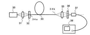
- an ultraviolet light emitting device is configured by the excitation light source 30, the condenser lenses 31 and 35, the dichroic mirror 32, the rare earth-doped optical waveguide 33, the excitation light cut filter 36, and the optical spectrum analyzer 38.
- the excitation light source 30 an optical parametric oscillator capable of converting a wavelength of a titanium sapphire laser and adjusting the wavelength from 340 nm to 500 nm and outputting pulsed light of 100 MHz repeatedly was used.
- the excitation light from the excitation light source 30 was condensed by the condenser lens 31 to the incident end 34a of the rare earth-doped optical waveguide 33 and optically coupled to the core portion of the end face 34a of the rare earth doped optical waveguide 33.
- the end face 34a of the rare earth-doped optical waveguide 33 was optically polished to a flat surface.
- a dichroic mirror 32 that transmits the excitation light wavelength band and reflects the ultraviolet light wavelength band is disposed to abut against the light incident end 34 a of the rare earth-doped optical waveguide 33.
- the dichroic mirror 32 was replaced for each kind of rare earth added to the rare earth-doped optical waveguide 33 in accordance with the wavelengths of the excitation light and the output light.
- the light propagating to the light incident end 34a side is folded back by the dichroic mirror 32 and emitted from the output end 34b.
- the light propagating toward the emission end 34b was emitted as it is from the emission end 34b.
- the exit end 34b was cleaved at an angle of 8 °, and the return loss was 60 dB or more.
- the emitted light is collected by the condensing lens 35, and after the excitation light is removed by the excitation light cut filter 36, the light is coupled to the measurement fiber end 37 of the optical spectrum analyzer 38 and is connected to the optical spectrum analyzer 38. Led. Then, the emission spectrum of the rare earth-doped optical waveguide 33 was measured by the optical spectrum analyzer 38.
- the rare-earth-doped optical waveguide 33 is a rare-earth-doped fluoride optical fiber doped with 0.3 mol% (about 3000 ppm) of rare-earth species RE (Nd, Gd and Er, Tb, Dy, Ho, Er, Tm).
- RE rare-earth species
- an Al-based fluoride fiber is used, and the glass composition is such that the core part is 32.8AlF 3 -15YF 3 -4.7LaF 3 -9.4MgF 2 -7.4CaF 2 -5.4SrF 2 -20BaF.
- the cladding part was 32.8AlF 3 ⁇ 15YF 3 ⁇ 5LaF 3 ⁇ 9.4MgF 2 ⁇ 8.4CaF 2 ⁇ 7.4SrF 2 ⁇ 17BaF 2 ⁇ 5BaCl 2 . All compositional numbers are mol%.
- REF 3 in the core composition represents a trifluoride of a rare earth species to be added.
- the core diameter was 3 ⁇ m
- the fiber diameter was 125 ⁇ m
- the fiber numerical aperture was 0.1
- the fiber length was 25 cm.
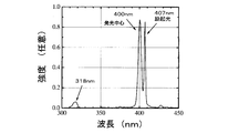
- FIG. 4 shows an emission spectrum when the additive rare earth species is excited at a wavelength of 407 nm in Er
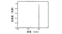
- FIG. 5 shows an emission spectrum when excited at a wavelength of 440 nm.
- the emitted light having emission center wavelengths of 400 nm and 318 nm was confirmed.
- the emission center wavelength obtained from the emission spectrum measurement when other rare earth species are added is shown in Table 1 together with the excitation wavelength. As can be seen from Table 1, in all the rare earths measured, emission of ultraviolet light having a wavelength shorter than the excitation light wavelength was observed.
- an ultraviolet laser oscillation device (ultraviolet light emitting device) is configured by the excitation light source 40, the condenser lenses 41 and 46, the dichroic mirror 42, the rare earth-doped optical waveguide 44, and the optical spectrum analyzer 48.
- the excitation light source 40 a GaN-based semiconductor laser capable of outputting laser light having a wavelength of 447 nm was used.
- the rare earth doped optical waveguide 44 was the same as the fluoride fiber doped with 3000 ppm Er used in Example 1. Further, the design reflection wavelength of the dichroic mirror 42 was 400 nm, and the wavelength of 420 nm or more was transmitted.
- the excitation light from the excitation light source 40 was condensed by the condenser lens 41, then transmitted through the dichroic mirror 42, and coupled to the core at the end face 43 of the rare earth-doped optical waveguide 44.
- the light propagating to the incident end 43 side was folded back by the dichroic mirror 42.
- the light propagating to the exit end 45 side is emitted from the exit end 45 and collected by the condenser lens 46 and reflected by the dichroic mirror 42. And branched into transmitted light.
- the reflected light from the dichroic mirror 42 was again optically coupled to the core at the end face of the incident end 43 of the rare earth-doped optical waveguide 44. Further, the transmitted light from the dichroic mirror 42 was optically coupled to the incident end 47 of the measurement fiber of the optical spectrum analyzer 48 and led to the optical spectrum analyzer 48. Then, the laser oscillation spectrum was measured with the optical spectrum analyzer 48.
- the ultraviolet light source device of the present invention can obtain ultraviolet light directly from the rare earth-doped optical waveguide, the structure can be simplified and miniaturized. Further, since ultraviolet light is radiated from the rare earth-doped optical waveguide, it is possible to provide an ultraviolet light source as a point light source with a simple configuration by reducing the core.
- the ultraviolet light source device of the present invention can emit ultraviolet light having a wavelength of 405 nm or less in the state of spontaneous emission light, amplified spontaneous emission light, or laser, measurement, processing, biotechnology, life science, medical treatment, etc. Available in the field.
- high-precision distance measurement and special measurement such as surface shape, interference measurement, surface modification, processing and marking of metals, ceramics, glass, crystals, polymers, etc., optical component inspection, semiconductor etching process, semiconductor manufacturing equipment and optics System testing, biofluorescent dye or fluorescent protein excitation, decomposition and synthesis of organic compounds, selective molecular cleavage and selective molecular binding, application to pharmaceutical synthesis including chemicals and intermediates, cell and chromosome processing, DNA, etc. It can be used for modification of specific molecules, surface cleaning, endoscopic treatment, endoscopic diagnosis, corneal treatment, and the like.
Landscapes
- Physics & Mathematics (AREA)
- Engineering & Computer Science (AREA)
- Optics & Photonics (AREA)
- Chemical & Material Sciences (AREA)
- Nanotechnology (AREA)
- Electromagnetism (AREA)
- Life Sciences & Earth Sciences (AREA)
- Biophysics (AREA)
- Crystallography & Structural Chemistry (AREA)
- Plasma & Fusion (AREA)
- Lasers (AREA)
Abstract
本発明によれば、励起光源と、励起光源からの励起光を吸収して光を発生するコア部を有する光導波路と、励起光源からの励起光を光導波路のコア部に光学的に結合する光学的結合部と、光導波路から発生した光を外部に放射する光放射部を備え、励起光源からの励起光は340nm~500nmの波長範囲から選ばれるいずれかの波長を有し、光導波路のコア部はNd、Gd、Tb、Dy、Ho、Er、Tmから選ばれる少なくとも一種類の希土類元素を含有し、光導波路から発生した光の波長は405nm以下かつ励起光波長よりも短波長であることを特徴とする、紫外光源装置が提供される。
Description
本発明は、簡易な構成で紫外光を発生する紫外光源装置に関する。
従来、紫外光源としては高圧水銀ランプやハロゲン系ランプなどのランプ光源、エキシマレーザに代表されるガスレーザ、固体レーザの波長変換によるレーザ装置などが知られている。特に近年ではファイバレーザを用いた波長変換による紫外光発生が盛んに研究されている。また、フッ化物結晶にNdを添加して77Kまで冷却し、赤外または590nmの黄色レーザで励起して紫外レーザ光を得た例がある(非特許文献1)。Ndを添加したフッ化物ファイバを590nmの黄色レーザで励起し、室温で紫外レーザ光を得た例(非特許文献2)および紫色レーザ光を得た例(非特許文献3)もある。しかしながら、Nd添加フッ化物結晶からの紫外発光または紫外レーザ発振は、低温冷却が必要であり、実用的でない。Nd添加フッ化物ファイバおよびNd添加フッ化物結晶の励起には、波長590nmの黄色レーザが使用されるが、このレーザは特殊なレーザであって簡易な構成では実現できない。具体的には、波長590nmの励起光源として、Arイオンレーザ励起の色素リングレーザを用いており、大型で調整も煩雑である。
紫外光を発生するランプ光源の特徴は、高電圧の電源によって発生する高エネルギーの放電内で、特定の分子や原子が乖離と再結合あるいは励起と脱励起を繰り返すことで、物質固有の多数の輝線を同時に得ることができる点である。このため、比較的広い波長範囲にわたって輝線を発生させることができる。一方、放電には一定の物理的な体積が必要であるため、広い範囲を照射するには適しているが、微小範囲の照射には不向きである。また、発光効率が低く発熱が非常に多い事から、空冷の場合は冷却ファンの音や振動や熱風、水冷の場合は装置が大型化するなどの問題がある。
エキシマレーザは、高出力紫外光を得ることができる上に、大面積のレーザ光を得られるという特徴があり、半導体製造分野で広く用いられている。しかし、エキシマレーザは発振媒質にハロゲン系のガスを使用しており、危険であるだけでなく、装置が大型であり整備も煩雑である。また、レーザ発振はパルス発振に限られるため、分光用途や検査用途では使用できない。これ以外のガスレーザとしてArイオンレーザが知られているが、レーザ発振効率は極めて低い。このため冷却装置など付帯設備が必要である。
固体レーザの波長変換は近年著しく進歩している。従来は固体レーザの波長変換に、LiNbO3(LN)やβ-BaB2O4(β-BBO)などの強誘電性光学結晶がバルク形状で使用されているが、変換効率が極めて低い。最近は高効率波長変換材料としてこれらの強誘電性光学結晶の導波路を周期分極反転したデバイスが使用されつつあり、従来のバルク型を遙かに上回る高効率が達成されている。しかし、周期分極反転素子として加工しなければならない分極周期は出力波長と関係があり、500nm以下の短波長では加工周期が短くなり作製が非常に困難である。また、最適な波長変換効率を維持するためには温度制御が必須であり、装置が複雑化する。
R.M.Macfarlane, F.Tong, A.J.Silversmith, and W.Lenth,"Violet cw neodymium upconversion laser ", Applied Physics Letter, vol.52, pp.1300-1302.
D.S.Funk, J.W.Carlson, and J.G.Eden,"Ultraviolet (381nm),room temperature laser in neodymium-doped fluorozirconate fibre", Electronics Letterd, vol.30, pp.1859-1860.
D.S.Funk, J.W.Carlson, and J.G.Eden,"Room-temperature fluorozirnae glass fiber laser in the violet (412nm)",Optics Letters, vol.20pp.1474-1476.
上記の通り、小型高効率で構成が単純な紫外光源装置は実現していない。
本発明は、このような従来の技術課題を解決し、小型高効率で構成が単純な紫外光源装置の提供を目的とするものである。
すなわち、本発明によれば、励起光源と、励起光源からの励起光を吸収して光を発生するコア部を有する光導波路と、励起光源からの励起光を光導波路のコア部に光学的に結合する光学的結合部と、光導波路から発生する光を外部に放射する光放射部を備え、励起光源からの励起光は340nm~500nmの波長範囲から選ばれるいずれかの波長を有し、光導波路のコア部はNd、Gd、Tb、Dy、Ho、Er、Tmから選ばれる少なくとも一種類の希土類元素を含有し、光導波路から発生する光の波長は405nm以下かつ励起光波長よりも短波長であることを特徴とする、紫外光源装置が提供される。
光導波路の少なくともコア部はフッ化物ガラス、フッ素酸化物ガラス、フツリン酸塩ガラスのいずれかからなることが好ましい。
添加光導波路で発生する自然放出光のうち、波長405nm以下の光を反射するミラーが、光導波路の光放射部と反対側の端面に配置され、光放射部から放射される光を自然放出光または増幅された自然放出光としてもよい。また、光導波路で発生する自然放出光のうち、波長が405nm以下の光を反射するミラーが、光導波路の両端面に配置され、光放射部より放射される光をレーザ光としてもよい。
以下、本発明について詳細に説明する。
図1は、本発明の第1実施形態に係る紫外光源装置12の概略図を示す。第1実施形態の紫外光源装置12は、励起光源1、集光レンズ2、ダイクロイックミラー3、希土類添加光導波路4、コリメートレンズ5、パワーモニタ用ミラー6、励起光カットフィルタ7、フォトダイオード8、制御回路9、出射ウィンドウ10、および電源プラグ11を備えている。
励起光源1からは波長340nmから500nmの範囲から選ばれるいずれかの波長の励起光が放出される。励起光源1と希土類添加光導波路4の間には集光レンズ2、ダイクロイックミラー3が設置され、励起光源1からの励起光は、集光レンズ2によって集光され、さらにダイクロイックミラー3を通して希土類添加光導波路4の入射端4aに集光されて、希土類添加光導波路4の入射端4a端面のコア部に光学的に結合される。コア部は、結合された励起光を吸収し、波長405nm以下かつ励起光波長よりも短波長で発光する。発光した光のうち、希土類添加光導波路4中を入射端4a側に伝搬するものは、ダイクロイックミラー3で全反射して折り返される。希土類添加光導波路4の光入射端4aと反対側の出射端4bに伝搬する光は、そのまま出射端4bから放射される。希土類添加光導波路4から放射された光は、コリメートレンズ5でコリメートされ、その先のパワーモニタ用ミラー6で反射光と透過光に分岐される。パワーモニタ用ミラー6を透過する光は、さらに出射ウィンドウ10を透過し、紫外光発生装置12から外部へ出射される。一方、パワーモニタ用ミラー6で反射された光は、励起光カットフィルタ7で励起光を除去した後、フォトダイオード8に入射され、光パワーに対応した電気信号に変換される。この電気信号は制御回路9に入力され、制御回路9は、紫外光発生装置12の出力が一定となるように演算することにより励起光源1の出力を制御する。制御回路9の駆動に必要な電気は電源プラグ11から得る。尚、第1実施形態では、集光レンズ2が光学的結合部(手段)を構成し、コリメートレンズ5、ミラー6及び出射ウィンドウ10が光放射部(手段)を構成している。
希土類添加光導波路4より外部へ放出された光を再度、希土類添加光導波路4の中へ結合するミラーは、入射端4に設けられたダイクロイックミラー3だけであるため、レーザ共振器は構成されていない。すなわち、紫外光源装置12の出射光は自然放出光(SE)または増幅された自然放出光(ASE)である。また、後述する実施例2のように、希土類添加光導波路4の両端4a、4bに波長405nm以下の光を反射するミラーを配置してレーザ共振器を構成することにより、紫外光源装置12の出射光をレーザ光とすることができる。図6のように1つのミラーを光導波路の両端に設けてもよいが、2つのミラーを光導波路の両端に別途設けてもよい。
図2は、本発明の第2実施形態に係る紫外光源装置26の概略図を示す。第2実施形態の紫外光源装置26は、励起光源20、透明サポート板21、希土類添加光導波路22、折り返し全反射ミラー23、コリメートレンズ24、励起光カットフィルタ25、制御基板、励起光源の電源、および筐体を備えている。但し、図2では制御基板、励起光源の電源、筐体などを省略して表示を簡略化している。
励起光源20には、波長340nmから500nmの範囲から選ばれるいずれかの波長の光を放出する平面発光体のような面状の広がりがある光源または点光源を多数アレイ状に配列した光源を用いる。一方、希土類添加光導波路22は、側面のクラッド部が励起光源20に対向した状態で、励起光波長で透明な透明サポート板21に固定されている。励起光源20からの励起光は、希土類添加光導波路22のクラッド部に照射される。希土類添加光導波路22のコア部にクラッド部を透過した励起光が結合されると、コア部は励起光を吸収して波長405nm以下かつ励起光波長よりも短波長で発光する。発生した光は光導波路22のコア中を伝搬する。希土類添加光導波路22の片側の端面に波長405nm以下の光を反射する反射ミラー23が設置され、反対側の端面に隣接してコリメートレンズ24が設置されている。希土類添加光導波路22のコア部で発生した光のうち、反射ミラー23側の端面に到達したものは、反射ミラー23で反射されて折り返される。この結果、希土類添加光導波路22のコア部で発生した光は全て、コリメートレンズ24側の端面から出射され、コリメートレンズ24でコリメートされ、さらに励起光カットフィルタ25で励起光を除去した後、紫外光源装置26の出射光として出射される。尚、第2実施形態では、透明サポート板21や希土類添加光導波路22のクラッド部が光学的結合部(手段)を構成し、コリメートレンズ24及びカットフィルタ25が光放射部(手段)を構成している。
希土類添加光導波路22より外部へ放出された光を再度、希土類添加光導波路22の中へ結合するミラーは反射ミラー23だけであるため、レーザ共振器は構成されていない。すなわち、紫外光源装置26の出射光は自然放出光(SE)または増幅された自然放出光(ASE)である。また、後述する実施例2のように、希土類添加光導波路22の両端に波長405nm以下の光を反射するミラーを配置してレーザ共振器を構成することにより、紫外光源装置26の出射光をレーザ光とすることができる。図6のように1つのミラーを光導波路の両端に設けてもよいが、2つのミラーを光導波路の両端に別途設けてもよい。
第1及び第2実施形態において、励起光源1、20は、波長340nmから500nmの範囲の波長で、励起に十分な光パワーを発生すれば特に限定されない。このような光源としては、GaN系半導体レーザ、GaN系LED、無機エレクトロルミネッセンス(無機EL)、有機エレクトロルミネッセンス(有機EL)、半導体レーザの出力を波長変換して得た二倍波、電子線励起蛍光体からの蛍光などが挙げられる。
中でもGaN系半導体レーザは高出力であり、しかも集光スポット径が小さいので、コア径が小さい希土類添加光導波路4、22であっても光学的な結合効率が高く、輝度の高い紫外光源を実現できる。
一方、LDアレイ、LEDアレイ、有機EL、無機ELなど二次元または三次元的に配置可能な光源は、希土類添加光導波路4、22への光学的な結合効率は低くなるものの、空間的に拡張が容易であり構造も簡単である。このため単位面積あたりの光密度は低いが、全光パワーとしては大きなパワーを放射可能であり、低い光学的な結合効率を補うことができる。このため、大きさの制約が厳しくない場合には、簡素な構造で紫外光を得られるので好ましい。
希土類添加光導波路4、22は、平面光導波路でもよいしファイバでも良い。希土類添加光導波路4、22のコア部には、Nd、Gd、Tb、Dy、Ho、Er、Tmから選ばれる少なくとも一種類の希土類元素が添加される。希土類元素の添加濃度は、励起光源1、20からの励起光の波長、励起光の出力、光導波路4、22の損失、光学構成、導波路4、22のコア直径、開口数など様々な要因で変化するため、一概には規定できないが、100ppmから50000ppmの範囲であることが好ましい。100ppm未満では励起光の吸収係数が低くなり単位長さあたりの発光量が低下し、光導波路4、22の損失を上回ることが困難となることから好ましくない。一方、50000ppmを超えるとガラス中への均一溶解が困難なだけでなく、希土類元素同士のエネルギー移譲による脱励起(濃度消光と呼ばれる)が生じ、発光効率が低下する。一般的には、GaN系半導体レーザ励起の場合1000ppmから10000ppmの範囲が、LEDアレイなど面状の励起光源を用いる場合は200ppmから5000ppmの範囲が適当である。
希土類添加光導波路4、22の少なくともコア部は、波長405nm以下の紫外波長域でも透明である必要があり、かつ短波長発光効率が高い低フォノン材料である必要がある。このようなガラスとしては、フッ化物ガラス、フッ素酸化物ガラス、フツリン酸塩ガラスが適している。中でもフッ化物ガラスは、作製の容易さと光学性能の点から、最も好ましい。フッ化物ガラス組成としては、Al系ガラス、Al-Zr系ガラス、Zr系ガラスが安定であり、好ましい。
希土類添加光導波路4、22中で発生した波長405nm以下の光は、希土類添加光導波路4、22内に閉じこめる割合を適切に制御することで、自然放出光(SE)または増幅された自然放出光(ASE)またはレーザ光として紫外光源装置12、26取り出すことができる。
自然放出光または増幅自然放出光の場合、広帯域光が得られるため、干渉計測では可干渉長が短く、分解能が向上する。また、形状計測では裏面反射の影響を受けにくく、レンズ形状などの高精度計測が可能である。また、生物用途では特定波長にエネルギーが集中しないため、同じ光パワーを照射しても生体サンプルが受けるダメージがレーザよりも少なく、照明用途や蛍光色素/蛍光タンパクの励起に好適である。
レーザ光の場合、狭帯域で干渉長が長いコヒーレント光が得られるだけでなく、自然放出光やASEよりも高出力な紫外光が得られる。このため、高出力が必要な加工用途として、表面微細加工、樹脂やガラスの微細加工、生体サンプルの部分的な破壊や細胞質の部分的な破壊、遺伝子の加工、リソグラフィーやエッチングなどの半導体プロセスへの適用などが可能である。また、可干渉長が長いので精密距離計測に適している。さらに、波長変換素子を組み合わせることで、波長200nm以下の光を得ることも可能である。この場合、200nm以下の紫外域でも透明性の高い非線形光学結晶を使用する必要があり、CsLiB6O10(CLBO)や、BaMgF4、BaZnF4、SrAlF5、Na2MgAlF7、Na2ZnAlF7などの強誘電性フッ化物結晶が適している。
発光波長と励起波長の関係は、励起条件、希土類濃度、ガラス組成、レーザ共振器条件などで変化するため一概に規定できない。例えばZr系フッ化物ガラスファイバにNdを添加し、波長430nmのGaN系半導体レーザで励起した場合、波長380nm帯で発光し、レーザ発振させることもできる。また、例えばZr系フッ化物ガラスファイバにTbを添加し、波長488nmのGaN系半導体レーザで励起した場合、波長380nm帯で発光し、レーザ発振させることもできる。また、例えばZr系フッ化物ガラスファイバにDyを添加し、波長400nmのGaN系半導体レーザで励起した場合、波長365nm帯で発光し、レーザ発振させることもできる。また、例えばZr系フッ化物ガラスファイバにHoを添加し、波長476nmのGaN系半導体レーザで励起した場合、波長385nm帯で発光し、レーザ発振させることもできる。また、例えばAl系フッ化物ガラスファイバにErを添加し、波長405nmのGaN系半導体レーザで励起した場合、波長318nm帯および400nm帯で発光し、これらの波長でレーザ発振させることもできる。また、例えばAl系フッ化物ガラスファイバにErを添加し、波長440nmのGaN系半導体レーザで励起した場合、318nm帯と400nm帯で発光し、レーザ発振させることもできる。また、例えばAl系フッ化物ガラスファイバにTmを添加し、波長358nmのGaN系半導体レーザで励起した場合、波長283nm帯と344nm帯で発光し、これらの波長でレーザ発振させることもできる。また、例えばAl系フッ化物ガラスファイバにErとGdを共に添加し、波長407nmまたは440nmのGaN系半導体レーザで励起した場合、310nm帯で発光し、レーザ発振させることもできる。
以下、実施例により本発明を詳細に説明するが、本発明はこれらの実施例に限定されるものではない。
各種希土類添加光導波路として用いて、下記の手順により各希土類種による紫外発光波長を調べた。
[実施例1]
図3に示すように、励起光源30、集光レンズ31、35、ダイクロイックミラー32、希土類添加光導波路33、励起光カットフィルタ36、光スペクトラムアナライザ38により紫外発光装置を構成した。励起光源30として、チタンサファイアレーザを波長変換し、波長340nmから500nmまで調整可能で、繰り返し100MHzのパルス光を出力できるオプティカルパラメトリック発振器を用いた。励起光源30からの励起光は、集光レンズ31で希土類添加光導波路33の入射端34aに集光され、希土類添加光導波路33の入射端34a端面のコア部に光学的に結合された。尚、希土類添加光導波路33の入射端34a端面は平面に光学研磨されていた。希土類添加光導波路33の光入射端34a端面には、励起光波長帯域を透過し紫外光波長帯域を反射するダイクロイックミラー32を突き当てて配置した。該ダイクロイックミラー32は、励起光と出力光の波長に合わせて、希土類添加光導波路33の添加されている希土類の種類毎に交換した。励起光によって希土類添加光導波路33のコア内で発生した光のうち、光入射端34a側へ伝搬する光は該ダイクロイックミラー32で折り返されて、出射端34bから放射された。また、希土類添加光導波路33のコア内で発生した光のうち、出射端34b側へ伝搬する光は、そのまま出射端34bから放射された。この出射端34bは8°斜めクリーブされており、反射減衰量は60dB以上であった。放射された光は、集光レンズ35で集光され、その先の励起光カットフィルタ36で励起光を除去した後、光スペクトラムアナライザ38の測定用ファイバ端37に結合され、光スペクトラムアナライザ38に導かれた。そして、光スペクトラムアナライザ38により希土類添加光導波路33の発光スペクトル測定を行った。
図3に示すように、励起光源30、集光レンズ31、35、ダイクロイックミラー32、希土類添加光導波路33、励起光カットフィルタ36、光スペクトラムアナライザ38により紫外発光装置を構成した。励起光源30として、チタンサファイアレーザを波長変換し、波長340nmから500nmまで調整可能で、繰り返し100MHzのパルス光を出力できるオプティカルパラメトリック発振器を用いた。励起光源30からの励起光は、集光レンズ31で希土類添加光導波路33の入射端34aに集光され、希土類添加光導波路33の入射端34a端面のコア部に光学的に結合された。尚、希土類添加光導波路33の入射端34a端面は平面に光学研磨されていた。希土類添加光導波路33の光入射端34a端面には、励起光波長帯域を透過し紫外光波長帯域を反射するダイクロイックミラー32を突き当てて配置した。該ダイクロイックミラー32は、励起光と出力光の波長に合わせて、希土類添加光導波路33の添加されている希土類の種類毎に交換した。励起光によって希土類添加光導波路33のコア内で発生した光のうち、光入射端34a側へ伝搬する光は該ダイクロイックミラー32で折り返されて、出射端34bから放射された。また、希土類添加光導波路33のコア内で発生した光のうち、出射端34b側へ伝搬する光は、そのまま出射端34bから放射された。この出射端34bは8°斜めクリーブされており、反射減衰量は60dB以上であった。放射された光は、集光レンズ35で集光され、その先の励起光カットフィルタ36で励起光を除去した後、光スペクトラムアナライザ38の測定用ファイバ端37に結合され、光スペクトラムアナライザ38に導かれた。そして、光スペクトラムアナライザ38により希土類添加光導波路33の発光スペクトル測定を行った。
ここで、希土類添加光導波路33には、希土類種RE(Nd、GdとEr、Tb、Dy、Ho、Er、Tm)が0.3mol%(約3000ppm)添加された希土類添加フッ化物光ファイバを用いた。具体的には、Al系フッ化物ファイバを用い、そのガラス組成は、コア部が32.8AlF3-15YF3-4.7LaF3-9.4MgF2-7.4CaF2-5.4SrF2-20BaF2-5BaCl2-0.3REF3で表され、クラッド部が32.8AlF3-15YF3-5LaF3-9.4MgF2-8.4CaF2-7.4SrF2-17BaF2-5BaCl2であった。組成の数字は全てモル%である。また、コア組成中のREF3は、添加する希土類種の三フッ化物を表している。コアの直径は3μm、ファイバの直径は125μm、ファイバの開口数は0.1、ファイバ長は25cmであった。
添加希土類種がErにおいて、波長407nmで励起した場合の発光スペクトルを図4に、波長440nmで励起した場合の発光スペクトルを図5に示す。いずれの場合も、発光中心波長が400nmおよび318nmの放射光を確認できた。同様にその他の希土類種が添加されている場合の発光スペクトル測定から求めた発光中心波長を励起波長とともに表1に示す。表1から分かるように、測定した全ての希土類において、励起光波長より短波長の紫外光の発光が認められた。

[実施例2]
図6に示すように、励起光源40、集光レンズ41、46、ダイクロイックミラー42、希土類添加光導波路44、光スペクトラムアナライザ48により紫外レーザ発振装置(紫外発光装置)を構成した。励起光源40として、波長447nmのレーザー光を出力できるGaN系半導体レーザを用いた。一方、希土類添加光導波路44には、実施例1で使用したErが3000ppm添加されているフッ化物ファイバと同じものを用いた。また、ダイクロイックミラー42の設計反射波長は400nmであり、420nm以上の波長は透過する特性を有していた。励起光源40からの励起光は、集光レンズ41で集光された後、ダイクロイックミラー42を透過して、希土類添加光導波路44の入射端43端面のコアに結合された。励起光によって希土類添加光導波路44のコア内で発生した光のうち、入射端43側に伝搬する光は、ダイクロイックミラー42で折り返された。励起光によって希土類添加光導波路44のコア内で発生した光のうち、出射端45側に伝搬する光は、出射端45から放射されて集光レンズ46で集光され、ダイクロイックミラー42で反射光と透過光に分岐された。ダイクロイックミラー42からの反射光は、再び希土類添加光導波路44の入射端43端面のコアに光学的に結合された。また、ダイクロイックミラー42からの透過光は、光スペクトラムアナライザ48の測定用ファイバの入射端47に光学的に結合され、光スペクトラムアナライザ48に導かれた。そして、光スペクトラムアナライザ48によりレーザ発振スペクトル測定を行った。
図6に示すように、励起光源40、集光レンズ41、46、ダイクロイックミラー42、希土類添加光導波路44、光スペクトラムアナライザ48により紫外レーザ発振装置(紫外発光装置)を構成した。励起光源40として、波長447nmのレーザー光を出力できるGaN系半導体レーザを用いた。一方、希土類添加光導波路44には、実施例1で使用したErが3000ppm添加されているフッ化物ファイバと同じものを用いた。また、ダイクロイックミラー42の設計反射波長は400nmであり、420nm以上の波長は透過する特性を有していた。励起光源40からの励起光は、集光レンズ41で集光された後、ダイクロイックミラー42を透過して、希土類添加光導波路44の入射端43端面のコアに結合された。励起光によって希土類添加光導波路44のコア内で発生した光のうち、入射端43側に伝搬する光は、ダイクロイックミラー42で折り返された。励起光によって希土類添加光導波路44のコア内で発生した光のうち、出射端45側に伝搬する光は、出射端45から放射されて集光レンズ46で集光され、ダイクロイックミラー42で反射光と透過光に分岐された。ダイクロイックミラー42からの反射光は、再び希土類添加光導波路44の入射端43端面のコアに光学的に結合された。また、ダイクロイックミラー42からの透過光は、光スペクトラムアナライザ48の測定用ファイバの入射端47に光学的に結合され、光スペクトラムアナライザ48に導かれた。そして、光スペクトラムアナライザ48によりレーザ発振スペクトル測定を行った。
測定されたレーザ発振スペクトルを図7に示す。波長401nmでレーザ発振が得られていることが確認できた。
上述の通り、本発明の紫外光源装置は、希土類添加光導波路から直接紫外光を得ることができるため、構造の簡素化及び小型化が可能である。また、希土類添加光導波路から紫外光が放射されるため、コアを小さくすることによって点光源の紫外光源を簡単な構成で提供することができる。
本発明を具体的な実施例に基づいて説明してきたが、本発明は上記実施例に限定されるものではなく、その趣旨を逸脱しない範囲で種々の変形・変更を含むものである。
本発明の紫外光源装置は、波長405nm以下の紫外光を、自然放出光、増幅された自然放出光、レーザの状態で放射することができることから、計測、加工、バイオ、ライフサイエンス、医療などの分野で利用できる。例えば、高精度な距離計測や表面形状などの特殊計測、干渉計測、表面改質、金属,セラミックス,ガラス,結晶,ポリマーなどの加工やマーキング、光学部品検査、半導体エッチングプロセス、半導体製造装置や光学系の検査、バイオ用蛍光色素または蛍光タンパク励起、有機化合物の分解や合成、選択的分子切断や選択的分子結合、化学薬品や中間体を含む医薬合成への応用、細胞や染色体加工、DNAなど特定分子の改変、表面洗浄、内視鏡治療、内視鏡診断、角膜治療などに利用できる。
Claims (4)
- 励起光源と、励起光源からの励起光を吸収して光を発生するコア部を有する光導波路と、励起光源からの励起光を光導波路のコア部に光学的に結合する光学的結合部と、光導波路から発生した光を外部に放射する光放射部を備え、励起光源からの励起光は340nm~500nmの波長範囲から選ばれるいずれかの波長を有し、光導波路のコア部はNd、Gd、Tb、Dy、Ho、Er、Tmから選ばれる少なくとも一種類の希土類元素を含有し、光導波路から発生した光の波長は405nm以下かつ励起光波長よりも短波長であることを特徴とする、紫外光源装置。
- 光導波路の少なくともコア部は、フッ化物ガラス、フッ素酸化物ガラス、フツリン酸塩ガラスのいずれかからなることを特徴とする、請求項1に記載の紫外光源装置。
- 光導波路で発生する自然放出光のうち、波長405nm以下の光を反射するミラーが、光導波路の放射部と反対側の端面に配置され、放射部から放射される光が自然放出光または増幅された自然放出光であることを特徴とする、請求項1または請求項2に記載の紫外光源装置。
- 光導波路で発生する自然放出光のうち、波長が405nm以下の光を反射するミラーが、光導波路の両端に配置され、放射部より放射される光がレーザ光であることを特徴とする、請求項1または請求項2に記載の紫外光源装置。
Applications Claiming Priority (2)
| Application Number | Priority Date | Filing Date | Title |
|---|---|---|---|
| JP2008-276285 | 2008-10-28 | ||
| JP2008276285A JP2010108956A (ja) | 2008-10-28 | 2008-10-28 | 紫外光源装置 |
Publications (1)
| Publication Number | Publication Date |
|---|---|
| WO2010050341A1 true WO2010050341A1 (ja) | 2010-05-06 |
Family
ID=42128707
Family Applications (1)
| Application Number | Title | Priority Date | Filing Date |
|---|---|---|---|
| PCT/JP2009/067398 Ceased WO2010050341A1 (ja) | 2008-10-28 | 2009-10-06 | 紫外光源装置 |
Country Status (2)
| Country | Link |
|---|---|
| JP (1) | JP2010108956A (ja) |
| WO (1) | WO2010050341A1 (ja) |
Cited By (1)
| Publication number | Priority date | Publication date | Assignee | Title |
|---|---|---|---|---|
| CN111487246A (zh) * | 2020-04-20 | 2020-08-04 | 中国农业科学院烟草研究所 | 一种烟草青枯病试纸条批次质量检测装置 |
Families Citing this family (1)
| Publication number | Priority date | Publication date | Assignee | Title |
|---|---|---|---|---|
| JP5919962B2 (ja) | 2011-04-22 | 2016-05-18 | セントラル硝子株式会社 | 弗素含有複合塩の製造方法 |
-
2008
- 2008-10-28 JP JP2008276285A patent/JP2010108956A/ja active Pending
-
2009
- 2009-10-06 WO PCT/JP2009/067398 patent/WO2010050341A1/ja not_active Ceased
Non-Patent Citations (2)
| Title |
|---|
| D.S. FUNK ET AL.: "Glass-fiber lasers in the ultraviolet and visible", IEEE JOURNAL OF SELECTED TOPICS IN QUANTUM ELECTRONICS, vol. 1, no. IS.3, September 1995 (1995-09-01), pages 784 - 791 * |
| JIANFU LI ET AL.: "Ultraviolet upconversion emission from ZBLAN glass doped with Tm3+ ions", PHYSICA B: CONDENSED MATTER, vol. 392, no. IS.1-2, 15 April 2007 (2007-04-15), pages 251 - 254 * |
Cited By (1)
| Publication number | Priority date | Publication date | Assignee | Title |
|---|---|---|---|---|
| CN111487246A (zh) * | 2020-04-20 | 2020-08-04 | 中国农业科学院烟草研究所 | 一种烟草青枯病试纸条批次质量检测装置 |
Also Published As
| Publication number | Publication date |
|---|---|
| JP2010108956A (ja) | 2010-05-13 |
Similar Documents
| Publication | Publication Date | Title |
|---|---|---|
| JP6142025B2 (ja) | 中赤外から遠赤外のダイヤモンド・ラマンレーザーシステム及び方法 | |
| Scholle et al. | 2 µm laser sources and their possible applications | |
| CN104737390B (zh) | 宽频带超连续光发射器件及其用途 | |
| JP2010026027A (ja) | 紫外レーザ装置 | |
| US7944954B2 (en) | Laser apparatus with all optical-fiber | |
| Fibrich et al. | Diode-pumped Pr: YAP lasers | |
| Hudson et al. | 1 W diode-pumped tunable Ho3+, Pr3+-doped fluoride glass fibre laser | |
| JP5098356B2 (ja) | 白色光発光材料および白色光発光装置 | |
| Baiocco et al. | Yellow diode-pumped lasing of femtosecond-laser-written Dy, Tb: LiLuF4 waveguide | |
| Nicolas et al. | 4f2 to 4f5d excited state absorption in Pr3+-doped crystals | |
| WO2010050341A1 (ja) | 紫外光源装置 | |
| EP4122061B1 (en) | Apparatus and method for adjusting the wavelength of light | |
| Baiocco et al. | Near infrared diode-pumped lasing of femtosecond-laser-written Pr: LiLuF4 waveguide | |
| Eliel et al. | Spectroscopic investigation and heat generation of Yb3+/Ho3+ codoped aluminosilicate glasses looking for the emission at 2 μm | |
| WO2013051354A1 (ja) | 太陽光励起レーザー装置、太陽光励起増幅装置および光増幅ガラス | |
| JP2010050126A (ja) | Ase光源 | |
| Cai et al. | Dual-wavelength competitive output in Nd: Y3Sc1. 5Al3. 5O12 ceramic disk laser | |
| Baiocco et al. | Overcoming the output power threshold of 400 mW with high-gain diode pumped Pr: LiLuF4 waveguide lasers | |
| CN110048300B (zh) | 基于磷酸钆晶体的激光器 | |
| Körner et al. | Temperature dependent spectroscopic characterization of Tm: YAG crystals as potential laser medium for pulsed high energy laser amplifiers | |
| Brandt et al. | Inband pumped Er: Lu2O3 and Er, Yb: YVO4 lasers near 1.6 μm for CO2 LIDAR | |
| Švejkar et al. | Passively Q-switched Er, La: SrF2-CaF2 laser at 2.74 μm | |
| Quan et al. | Growth, spectroscopic, and 2.7-μm Q-switched laser properties of Cr, Er: YAP crystal by xenon-lamp pumping | |
| Balakrishnaiah et al. | Infrared to UV, VIS and NIR frequency upconversion luminescence studies of Tm3+-doped YbLiF4 crystal | |
| Eichler et al. | High power diode and solid state lasers |
Legal Events
| Date | Code | Title | Description |
|---|---|---|---|
| 121 | Ep: the epo has been informed by wipo that ep was designated in this application |
Ref document number: 09823454 Country of ref document: EP Kind code of ref document: A1 |
|
| NENP | Non-entry into the national phase |
Ref country code: DE |
|
| 122 | Ep: pct application non-entry in european phase |
Ref document number: 09823454 Country of ref document: EP Kind code of ref document: A1 |