WO2010050125A1 - Cpp-gmr素子、tmr素子および磁気記録再生装置 - Google Patents
Cpp-gmr素子、tmr素子および磁気記録再生装置 Download PDFInfo
- Publication number
- WO2010050125A1 WO2010050125A1 PCT/JP2009/005183 JP2009005183W WO2010050125A1 WO 2010050125 A1 WO2010050125 A1 WO 2010050125A1 JP 2009005183 W JP2009005183 W JP 2009005183W WO 2010050125 A1 WO2010050125 A1 WO 2010050125A1
- Authority
- WO
- WIPO (PCT)
- Prior art keywords
- film
- mnir
- layer
- ptmn
- aucu
- Prior art date
- Legal status (The legal status is an assumption and is not a legal conclusion. Google has not performed a legal analysis and makes no representation as to the accuracy of the status listed.)
- Ceased
Links
Images







Classifications
-
- B—PERFORMING OPERATIONS; TRANSPORTING
- B82—NANOTECHNOLOGY
- B82Y—SPECIFIC USES OR APPLICATIONS OF NANOSTRUCTURES; MEASUREMENT OR ANALYSIS OF NANOSTRUCTURES; MANUFACTURE OR TREATMENT OF NANOSTRUCTURES
- B82Y25/00—Nanomagnetism, e.g. magnetoimpedance, anisotropic magnetoresistance, giant magnetoresistance or tunneling magnetoresistance
-
- G—PHYSICS
- G01—MEASURING; TESTING
- G01R—MEASURING ELECTRIC VARIABLES; MEASURING MAGNETIC VARIABLES
- G01R33/00—Arrangements or instruments for measuring magnetic variables
- G01R33/02—Measuring direction or magnitude of magnetic fields or magnetic flux
- G01R33/06—Measuring direction or magnitude of magnetic fields or magnetic flux using galvano-magnetic devices
- G01R33/09—Magnetoresistive devices
- G01R33/093—Magnetoresistive devices using multilayer structures, e.g. giant magnetoresistance sensors
-
- G—PHYSICS
- G01—MEASURING; TESTING
- G01R—MEASURING ELECTRIC VARIABLES; MEASURING MAGNETIC VARIABLES
- G01R33/00—Arrangements or instruments for measuring magnetic variables
- G01R33/02—Measuring direction or magnitude of magnetic fields or magnetic flux
- G01R33/06—Measuring direction or magnitude of magnetic fields or magnetic flux using galvano-magnetic devices
- G01R33/09—Magnetoresistive devices
- G01R33/098—Magnetoresistive devices comprising tunnel junctions, e.g. tunnel magnetoresistance sensors
-
- G—PHYSICS
- G11—INFORMATION STORAGE
- G11B—INFORMATION STORAGE BASED ON RELATIVE MOVEMENT BETWEEN RECORD CARRIER AND TRANSDUCER
- G11B5/00—Recording by magnetisation or demagnetisation of a record carrier; Reproducing by magnetic means; Record carriers therefor
- G11B5/127—Structure or manufacture of heads, e.g. inductive
- G11B5/33—Structure or manufacture of flux-sensitive heads, i.e. for reproduction only; Combination of such heads with means for recording or erasing only
- G11B5/39—Structure or manufacture of flux-sensitive heads, i.e. for reproduction only; Combination of such heads with means for recording or erasing only using magneto-resistive devices or effects
- G11B5/3903—Structure or manufacture of flux-sensitive heads, i.e. for reproduction only; Combination of such heads with means for recording or erasing only using magneto-resistive devices or effects using magnetic thin film layers or their effects, the films being part of integrated structures
- G11B5/3906—Details related to the use of magnetic thin film layers or to their effects
-
- H—ELECTRICITY
- H01—ELECTRIC ELEMENTS
- H01F—MAGNETS; INDUCTANCES; TRANSFORMERS; SELECTION OF MATERIALS FOR THEIR MAGNETIC PROPERTIES
- H01F10/00—Thin magnetic films, e.g. of one-domain structure
- H01F10/32—Spin-exchange-coupled multilayers, e.g. nanostructured superlattices
- H01F10/324—Exchange coupling of magnetic film pairs via a very thin non-magnetic spacer, e.g. by exchange with conduction electrons of the spacer
- H01F10/3268—Exchange coupling of magnetic film pairs via a very thin non-magnetic spacer, e.g. by exchange with conduction electrons of the spacer the exchange coupling being asymmetric, e.g. by use of additional pinning, by using antiferromagnetic or ferromagnetic coupling interface, i.e. so-called spin-valve [SV] structure, e.g. NiFe/Cu/NiFe/FeMn
-
- H—ELECTRICITY
- H10—SEMICONDUCTOR DEVICES; ELECTRIC SOLID-STATE DEVICES NOT OTHERWISE PROVIDED FOR
- H10N—ELECTRIC SOLID-STATE DEVICES NOT OTHERWISE PROVIDED FOR
- H10N50/00—Galvanomagnetic devices
- H10N50/10—Magnetoresistive devices
Definitions
- the present invention relates to a magnetoresistive effect element such as a CPP-GMR element or a TMR element to which an L1 0 MnIr-based antiferromagnetic layer is applied, and a magnetic recording / reproducing apparatus using the magnetoresistive effect element [hard disk drive (HDD) or spin random access memory ( SPRAM)].
- a magnetoresistive effect element such as a CPP-GMR element or a TMR element to which an L1 0 MnIr-based antiferromagnetic layer is applied
- a magnetic recording / reproducing apparatus using the magnetoresistive effect element [hard disk drive (HDD) or spin random access memory ( SPRAM)].
- Magnetoresistance effect elements such as CPP-GMR (current-perpendicular-to-the-planet-Giant-magnetoresistive) elements and TMR (Tunneling-magnetoresistive) elements are known as high-density magnetic recording / reproducing magnetic sensors.
- CPP-GMR current-perpendicular-to-the-planet-Giant-magnetoresistive
- TMR Tunnelneling-magnetoresistive
- the CPP-GMR element includes a laminated structure formed on a suitable material including a ferromagnetic film (1) and a ferromagnetic film (2) separated by a conductive nonmagnetic intermediate layer.
- a typical CPP-GMR element structure is lower electrode / antiferromagnetic layer / ferromagnetic film (1) / conductive nonmagnetic intermediate layer / ferromagnetic film (2) / upper electrode.
- the uppermost layer is the upper electrode and the lowermost layer is the lower electrode, and the following laminated film is also expressed in this way.
- the magnetization direction of the ferromagnetic film (1) is fixed in a direction perpendicular to the magnetization direction of the ferromagnetic film (2) when the externally applied magnetic field is zero.
- the magnetization direction of the ferromagnetic film (1) is fixed in such a way that the antiferromagnetic film is adjacent and the ferromagnetic film (1) is anisotropic in one direction by exchange coupling between the antiferromagnetic film and the ferromagnetic film (1). This is done by imparting sex energy or exchange magnetic anisotropy energy. Therefore, the ferromagnetic film (1) is called a fixed layer or a fixed-side ferromagnetic film, and is expressed in this specification as well.
- a typical magnetization fixing direction of the fixed layer is a direction perpendicular to the medium facing surface and the air bearing surface (ABS surface).
- the magnetization direction of the ferromagnetic film (2) can be freely rotated by an externally applied magnetic field. Therefore, the ferromagnetic film (2) is called a free layer or a free-side ferromagnetic film, and is expressed in this specification as well.
- a magnetic field generated from a magnetic medium is used as an applied magnetic field, and the magnetization direction of the free layer freely rotates in accordance with the magnetic field. As a result, the angle formed between the magnetization direction of the fixed layer and the magnetization direction of the free layer Changes.
- the CPP-GMR element uses a magnetoresistive transformer that converts a magnetic signal from a magnetic medium into an electrical signal by utilizing the fact that the electrical resistance changes according to the change in the angle between the magnetization directions of the fixed layer and the free layer.
- I ’m a Deucer.
- an MR ratio of more than 20% is obtained by using a so-called half metal film for the free layer or the fixed layer, or introducing a technique called current confinement for the conductive nonmagnetic intermediate layer. .
- the TMR element contains a laminated structure formed on an appropriate material including the ferromagnetic film (1) and the ferromagnetic film (2) separated by the insulating barrier layer.
- a typical TMR element structure is: lower electrode / antiferromagnetic film / ferromagnetic film (1) / insulating barrier layer / ferromagnetic film (2) / upper electrode.
- the role of each film and the operating principle of the TMR element are the same as those of the CPP-GMR element described above except that an insulating barrier layer is used and the upper and lower energization is performed using the tunnel effect.
- an MR ratio exceeding 350% is obtained by adopting a CoFeB / MgO / CoFeB structure for the fixed layer, the insulating barrier layer, and the free layer.
- the key technologies for increasing the density and improving the characteristics are the fixed layer / conductive nonmagnetic intermediate layer, conductive nonmagnetic intermediate layer / free layer, and fixed layer / insulating barrier layer.
- an irregular phase FeMn film, a NiO film, a CrMnPt film, an L1 0 PtMn film, an L1 0 PtPdMn film, an irregular phase MnIr film, an ordered phase Mn 75 Ir 25 film, etc. are known. It has been. At present, irregular-phase MnIr films and ordered-phase Mn 75 Ir 25 films are used as industry standards. Incidentally, the ordered phase Mn 75 Ir 25 film is known to be able to impart the largest exchange magnetic anisotropy energy constant of about 1.3 erg / cm 2 among the antiferromagnetic films. (See Patent Document 1, Non-Patent Document 1, and Non-Patent Document 2)
- the antiferromagnetic film Since the disordered MnIr film has a cubic crystal structure (fcc), the antiferromagnetic film has a magnetocrystalline anisotropy energy constant (K AF ) on the order of 10 5 erg / cm 3 and is small.
- the ordered-phase Mn 75 Ir 25 film also has a giant exchange magnetic anisotropy energy constant (K e ) of about 1.3 erg / cm 2 , but because the crystal structure is fcc, K AF is It is on the order of 10 5 erg / cm 3 and is small.
- an ordered phase L1 0 MnIr film having K AF ⁇ 2 ⁇ 10 8 erg / cm 3 predicted by first-principles calculation is applied to the antiferromagnetic film for the fixed layer.
- a representative CPP-GMR element of the present invention includes at least a seed layer, an antiferromagnetic film, a ferromagnetic film, a fixed-side ferromagnetic layer, a nonmagnetic conductive intermediate layer, an external layer on a lower electrode.
- the antiferromagnetic film is composed of an L1 0 MnIr-based antiferromagnetic film having a crystalline magnetic anisotropy energy constant of 10 8 erg / cm 3 or more or an order of 0.8 or more.
- a typical TMR element of the present invention has a seed layer, an antiferromagnetic film, a ferromagnetic film, a fixed-side ferromagnetic layer, an insulating barrier layer, and an external magnetic field on the lower electrode.
- a TMR element having a free-side ferromagnetic layer whose magnetization direction freely changes and an upper electrode The antiferromagnetic film is composed of an L1 0 MnIr-based antiferromagnetic film having a crystalline magnetic anisotropy energy constant of 10 8 erg / cm 3 or more or an order of 0.8 or more.
- L1 0 ordered phase of MnIr film to produce an irregular / ordered phase transformation (ordered) in other words MnIr film, drawing equilibrium, it is about 1/2 of the melting point High temperature heat treatment at about 600 ° C. or formation while heating is required.
- the thin film is in a non-equilibrium state and various low temperature ordering techniques can be used to reduce the temperatures mentioned above. Therefore, the present invention provides the following three solutions for low-temperature ordering of MnIr films.
- AuCu-based, PtMn-based dynamic stress-driven MnIr film low-temperature ordering (2) Static stress driven MnIr film low-temperature ordering by precious metal seed arrangement, (3)
- high Ar pressure film-driven MnIr film is ordered at low temperature.
- an antiferromagnetic film for a fixed layer that can be used up to the end of a magnetoresistive effect element such as a CPP-GMR / TMR element even if the element size is extremely small to cope with ultra-high density. it can.
- a magnetoresistive effect element such as a CPP-GMR / TMR element
- the element size is 10 nm ⁇ and the L1 0 MnIr film thickness is 5 nm
- the (K AF V AF ) / (k B T) value is about 2416.
- K AF V AF ) / (k B T) value of about 604.
- the (K AF V AF ) / (k B T) value is about 151.
- ⁇ 1.2 ⁇ 10 49 years and an astronomical numerical value of thermal fluctuation resistance are obtained. It is done.
- FIG. 1 is an enlarged cross-sectional view of a CPP-GMR element to which an L1 0 MnIr antiferromagnetic film is applied according to Example 1.
- FIG. 1 is an enlarged cross-sectional view of a TMR element to which an L1 0 MnIr antiferromagnetic film is applied according to Example 1.
- FIG. 10 is an enlarged cross-sectional view of a CPP-GMR element in which an L1 0 MnIr antiferromagnetic film is applied and a dynamic stress driving layer is newly provided thereon according to Example 2. It is an expanded sectional view of the TMR element which applied the L1 0 MnIr antiferromagnetic film
- FIG. 1 It is a figure which shows the lattice parameter in the (111) plane of an AuCu dynamic stress drive layer and a MnIr film
- FIG. 6 is an enlarged cross-sectional view of a CPP-GMR element in which an L1 0 MnIr antiferromagnetic film is applied, a dynamic stress driving layer is provided, and a noble metal seed static stress driving layer is newly provided thereon according to Example 3. .
- FIG. 6 is a diagram for explaining static stress-driven MnIr low-temperature ordering by a noble metal seed according to Example 3. It is a figure for demonstrating the high Ar pressure film-forming drive MnIr low-temperature ordering by Example 3.
- 1 is a configuration diagram of a hard disk drive (HDD) to which a CPP-GMR element or a TMR element is applied according to the present invention.
- HDD hard disk drive
- 1 is a configuration diagram of a spin random access memory (SPRAM) to which a TMR element is applied according to the present invention. It is the schematic which shows the direction of the magnetization vector of a fixed layer at the time of "0" "1" recording state of a spin random access memory.
- SPRAM spin random access memory
- the antiferromagnetic film 300 for the fixed layer is formed of an L1 0 MnIr antiferromagnetic film.
- the lower electrode 100 is made of a Ru film and has a thickness of 50 nm.
- the seed layer 200 is composed of a Ta / Cu laminated film, and the film thickness is 5 nm.
- the film thickness of the L1 0 MnIr antiferromagnetic film 300 is 5 nm.
- the ferromagnetic film (1-a) 401 is composed of a Co film and has a thickness of 1.5 nm.
- the ferromagnetic film (1-b) 402 is composed of a half-metal CoMnSi film and has a thickness of 3 nm.
- the conductive nonmagnetic intermediate layer 501 is composed of a Cu—Al—O film and has a thickness of 2 nm.
- the ferromagnetic film (2) 600 is composed of a half-metal CoMnSi film and has a thickness of 3 nm.
- the upper electrode 700 is made of a Ru film and has a film thickness of 50 nm.
- the ferromagnetic film (1-a) 401 and the ferromagnetic film (1-b) 402 are firmly fixed by ferromagnetic / ferromagnetic exchange coupling.
- K e 4 ⁇ z ⁇ ⁇ ⁇ 3/2 ⁇ ⁇ (A AF ⁇ K AF ) (z: number of re-adjacent atoms, A AF : When the theoretical value of K e was popped out using the relational expression (exchange step constants), a value of about 80 erg / cm 2 was obtained.
- the above-described fixed layer ferromagnetic film (1-a) 401 / ferromagnetic film (1-b) 402 laminated film
- ferromagnetic film (1-a) 401 / ferromagnetic film (1-b) 402 laminated film ideally, an exchange magnetic anisotropy energy constant of about 80 erg / cm 2 can be imparted.
- the L1 0 PtMn antiferromagnetic film is known to have a similar crystal structure and magnetic structure as the L1 0 MnIr antiferromagnetic film, and the valid exchange coupling model is also the same Malzemoff model.
- the experimental value of K e of this L1 0 PtMn antiferromagnetic film is about 0.4 erg / cm 2 .
- the K AF of L1 0 PtMn predicted from the first-principles calculation is about 1/20 of L1 0 MnIr. In other words, the K AF of L1 0 MnIr is about 20 times that of L1 0 PtMn.
- the fixed layer the ferromagnetic film (1-a) 401 / the ferromagnetic film (1-b) 402 laminated film is experimentally used. It was found to be imparted a K e about 1.8erg / cm 2 extremely large exchange anisotropy energy constant. The K e of about 1.8 erg / cm 2 is a value exceeding about 1.3 erg / cm 2 of the conventional known Mn 75 Ir 25 antiferromagnetic film.
- the L1 0 MnIr blocking temperature T B of the diamagnetic film since the L1 0 MnIr of T N is even about 867 ° C, it is difficult to measure by broken is very high, film.
- the crystal structure, magnetic structure is similar, appropriate exchange coupling model is the same L1 0 PtMn, L1 0 NiMn T B of the antiferromagnetic film is in the approximate 200 ° C lower temperature than T N, it From this analogy, it is estimated that TB exceeds about 600 ° C.
- the (K AF V AF ) / (k B T) value is about 2416.
- K AF V AF ) / (k B T) value is about 604.
- the (K AF V AF ) / (k B T) value is about 151. It can be seen that the heat fluctuation resistance is extremely high.
- ⁇ 1.2 ⁇ 10 49 years and the thermal fluctuation resistance value of astronomical values are as follows. can get. In other words, it takes 1.2 ⁇ 10 49 years before the anisotropy axis of the L1 0 MnIr antiferromagnetic film collapses. From the above, even if the element size becomes extremely small by using the L1 0 MnIr film as the antiferromagnetic film for the fixed layer, it is possible to use the fixed layer to the end of the magnetoresistive effect element such as the CPP-GMR / TMR element. An antiferromagnetic film can be provided.
- the above thermal fluctuation resistance is the case where the K AF of the L1 0 MnIr antiferromagnetic film is about 2 ⁇ 10 8 erg / cm 3 and the order S is about 1, but the order S is actually 1 Hard to get.
- the K AF of the L1 0 MnIr antiferromagnetic film is on the order of 10 8 erg / cm 3 , and it is sufficient that the degree of order S is 0.8 or more.
- the composition of the L1 0 MnIr antiferromagnetic film according to the present invention is at.
- the percentage ratio is approximately 50:50, but it may be slightly shifted because the composition margin is wide.
- Pt, Pd, Rh, Au, Ag, Ru, etc. % To several 10 at. %, Or a combination of these two or more precious metals may be added.
- FIG. 1 shows a basic CPP-GMR structure of the L1 0 MnIr antiferromagnetic film bottom type, but it may be a L1 0 MnIr antiferromagnetic film top type, and further sandwiched to have a dual structure. It is good as a type.
- a laminated ferrimagnetic structure film made of, for example, an irregular phase MnIr / NiFe / Ru / NiFe may be provided below the L1 0 MnIr antiferromagnetic film 300.
- an upper laminated ferri-structured film or a dual laminated ferri-structured film may be provided.
- a Co film [ferromagnetic film (1-a)] is interposed in order to obtain a high-quality half-metal CoMnSi film [ferromagnetic film (1-b)].
- the film (1-a) may be omitted.
- a seed layer 200 and at least L1 on the lower electrode 100, to which an L1 0 MnIr antiferromagnetic film having a magnetocrystalline anisotropy energy constant K AF 2 ⁇ 10 8 erg / cm 3 is applied.
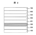
- an MnIr antiferromagnetic film 300 a ferromagnetic film (1-a) 401 that forms part of the fixed layer, a ferromagnetic film (1-b) 402 that forms part of the fixed layer, an insulating barrier layer 502, 1 shows an enlarged cross-sectional view of a TMR element including a magnetic multilayer film formed by sequentially laminating a ferromagnetic film (2) 600 serving as a free layer and an upper electrode 700 as viewed from a medium facing surface, a so-called ABS surface. .
- the antiferromagnetic film 300 for the fixed layer is formed of an L1 0 MnIr antiferromagnetic film.
- the lower electrode 100 is made of a Ru film and has a thickness of 50 nm.
- the seed layer 200 is composed of a Ta / Cu laminated film, and the film thickness is 5 nm.
- the film thickness of the L1 0 MnIr antiferromagnetic film 300 is 5 nm.
- the ferromagnetic film (1-a) 401 is composed of a Co film and has a thickness of 1.5 nm.
- the ferromagnetic film (1-b) 402 is composed of a CoFeB film and has a thickness of 4 nm.
- the insulating barrier layer 502 is composed of an MgO film and has a thickness of 1.5 nm.
- the ferromagnetic film (2) 600 is composed of a CoFeB film and has a film thickness of 4 nm.
- the upper electrode 700 is made of a Ru film and has a film thickness of 50 nm.
- the ferromagnetic film (1-a) 401 and the ferromagnetic film (1-b) 402 are firmly fixed by ferromagnetic / ferromagnetic exchange coupling.
- K AF 2 ⁇ 10 8 erg / cm 3 and regularity S ⁇ 1 of the L1 0 MnIr antiferromagnetic film.
- the regularity S often falls to about 0.8.
- the K AF of the L1 0 MnIr antiferromagnetic film is on the order of 10 8 erg / cm 3 , and it is sufficient that the degree of order S is 0.8 or more.
- the composition of the L1 0 MnIr antiferromagnetic film according to the present invention is at.
- the percentage ratio is approximately 50:50, but it may be slightly shifted because the composition margin is wide.
- Pt, Pd, Rh, Au, Ag, Ru, etc. % To several 10 at. %, Or a combination of these two or more precious metals may be added.
- FIG. 2 shows the basic TMR structure of the L1 0 MnIr antiferromagnetic film bottom type, but it may be the L1 0 MnIr antiferromagnetic film top type, and further sandwiched as a dual structure type. Also good.
- a laminated ferrimagnetic structure film made of, for example, NiFe / Ru / NiFe may be provided above the L1 0 MnIr antiferromagnetic film 300.
- the upper laminated ferri structure film may be provided, and in the case of the dual structure type, a dual laminated ferri structure film may be provided.
- a Co film [ferromagnetic film (1-a) 401] is interposed in order to obtain a good quality CoFeB film [ferromagnetic film (1-b) 402].
- the film (1-a) may be omitted.
- a PtMn dynamic stress driving layer is newly provided, and at least on the lower electrode 100, the seed layer 200, the AuCu or PtMn dynamic stress driving layer 250, and the L1 0 MnIr antiferromagnetic film 300,
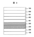
- the role of the ferromagnetic film (1-a) 401 forming part of the fixed layer, the ferromagnetic film (1-b) 402 forming part of the fixed layer, the conductive nonmagnetic intermediate layer 501 and the free layer 1 is an enlarged cross-sectional view of a CPP-GMR element including a magnetic laminated film formed by sequentially laminating a ferromagnetic film (2) 600 that bears the upper electrode 700 and a medium facing surface, that
- antiferromagnetic layer 300 for fixing layer is composed of L1 0 MnIr antiferromagnetic film, thereon, AuCu to facilitate cold rules of L1 0 MnIr antiferromagnetic film, or PtMn
- a system dynamic stress driving layer 250 is provided.
- the lower electrode 100 is made of a Ru film and has a thickness of 50 nm.
- the seed layer 200 is composed of a Ta / Cu laminated film, and the film thickness is 5 nm.
- the dynamic stress driving layer 250 has a composition ratio of at. It is composed of an AuCu film at a ratio of approximately 50:50, and the film thickness is 10 nm.
- the film thickness of the L1 0 MnIr antiferromagnetic film 300 is 5 nm.
- the ferromagnetic film (1-a) 401 is composed of a Co film and has a thickness of 1.5 nm.
- the ferromagnetic film (1-b) 402 is composed of a half-metal CoMnSi film and has a thickness of 3 nm.
- the conductive nonmagnetic intermediate layer 501 is composed of a Cu—Al—O film and has a thickness of 2 nm.
- the ferromagnetic film (2) 600 is composed of a half-metal CoMnSi film and has a thickness of 3 nm.
- the upper electrode 700 is made of a Ru film and has a film thickness of 50 nm.
- the ferromagnetic film (1-a) 401 and the ferromagnetic film (1-b) 402 are firmly fixed by ferromagnetic / ferromagnetic exchange coupling.
- the AuCu or by providing a PtMn-based dynamic stress drive layer, a low temperature heat treatment (350 ° C or less), described in Example 1, L1 0 MnIr antiferromagnetic film of K e experimental value about 1.8Erg / cm 2, T B value 600 ° C greater, and, even as a very small element size, the thermal fluctuation resistance value of the astronomical numerical can be easily obtained.
- composition of the AuCu dynamic stress driving layer according to this example is as described above.
- the percentage ratio is approximately 50:50, but it may be slightly shifted because the composition margin is wide.
- Pt, Pd, Rh, Ir, Ag, Ru, Fe, Co, Ni, etc. % May be added. Further, these two or more elements may be added in combination.
- the percentage ratio is approximately 50:50, but it may be slightly shifted because the composition margin is wide.
- Au, Pd, Rh, Ir, Ag, Ru, Fe, Co, Ni, etc. % May be added. Further, these two or more elements may be added in combination.
- the seed layer 200 may not be provided. This is because the AuCu-based film shows a good dense surface (111) orientation without a seed layer.
- FIG. 3 shows a basic CPP-GMR structure of an underlay type of AuCu or PtMn based dynamic stress driving layer / L1 0 MnIr antiferromagnetic film.
- a laminated ferrimagnetic structure film made of, for example, NiFe / Ru / NiFe may be provided above the L1 0 MnIr antiferromagnetic film 300.
- an L1 0 MnIr antiferromagnetic film / AuCu or PtMn based dynamic stress drive layer is provided with an overlying laminated ferristructure film, and with a dual structure type, a dual laminated ferristructure film is provided. But it ’s good.
- a PtMn dynamic stress driving layer is newly provided, and at least on the lower electrode 100, the seed layer 200, the AuCu or PtMn dynamic stress driving layer 250, and the L1 0 MnIr antiferromagnetic film 300,
- antiferromagnetic layer 300 for fixing layer is composed of L1 0 MnIr antiferromagnetic film, thereon, AuCu to facilitate cold rules of L1 0 MnIr antiferromagnetic film, or PtMn
- a system dynamic stress driving layer 250 is provided.
- the lower electrode 100 is made of a Ru film and has a thickness of 50 nm.
- the seed layer 200 is composed of a Ta / Cu laminated film, and the film thickness is 5 nm.
- the dynamic stress driving layer 250 has a composition ratio of at. It is composed of an AuCu film at a ratio of approximately 50:50, and the film thickness is 10 nm.
- the film thickness of the L1 0 MnIr antiferromagnetic film 300 is 5 nm.
- the ferromagnetic film (1-a) 401 is composed of a Co film and has a thickness of 1.5 nm.
- the ferromagnetic film (1-b) 402 is composed of a CoFeB film and has a thickness of 4 nm.
- the insulating barrier layer 502 is composed of an MgO film and has a thickness of 1.5 nm.
- the ferromagnetic film (2) 600 is composed of a CoFeB film and has a film thickness of 4 nm.
- the upper electrode 700 is made of a Ru film and has a film thickness of 50 nm.
- the ferromagnetic film (1-a) 401 and the ferromagnetic film (1-b) 402 are firmly fixed by ferromagnetic / ferromagnetic exchange coupling.
- the AuCu or by providing a PtMn-based dynamic stress drive layer, a low temperature heat treatment (350 ° C or less), described in Example 1, L1 0 MnIr antiferromagnetic film of K e experimental value about 1.8Erg / cm 2, T B value 600 ° C greater, and, even as a very small element size, the thermal fluctuation resistance value of the astronomical numerical can be easily obtained.
- composition of the AuCu dynamic stress driving layer according to this example is as described above.
- the percentage ratio is approximately 50:50, but it may be slightly shifted because the composition margin is wide.
- Pt, Pd, Rh, Ir, Ag, Ru, Fe, Co, Ni, etc. % May be added. Further, these two or more elements may be added in combination.
- the percentage ratio is approximately 50:50, but it may be slightly shifted because the composition margin is wide.
- Au, Pd, Rh, Ir, Ag, Ru, Fe, Co, Ni, etc. % May be added. Further, these two or more elements may be added in combination.
- the seed layer may not be provided. This is because the AuCu-based film shows a good dense surface (111) orientation without a seed layer.
- FIG. 4 shows a basic TMR structure of an underlay type of AuCu or PtMn dynamic stress driving layer / L1 0 MnIr antiferromagnetic film.
- the layer 250 / upper electrode 700 may be an L1 0 MnIr antiferromagnetic film / AuCu, or a PtMn based dynamic stress driving layer may be placed on the top, or may be sandwiched, for example, the lower electrode 100 / seed layer 200 / AuCu, or PtMn-based dynamic stress driving layer 250 / L1 0 MnIr antiferromagnetic film 300 / ferromagnetic film (1-a) 401 / ferromagnetic
- a laminated ferrimagnetic structure film made of, for example, NiFe / Ru / NiFe may be provided above the L1 0 MnIr antiferromagnetic film 300.
- an L1 0 MnIr antiferromagnetic film / AuCu or PtMn based dynamic stress drive layer is provided with an overlying laminated ferristructure film, and with a dual structure type, a dual laminated ferristructure film is provided. But it ’s good.
- the crystal structures of the AuCu or PtMn film and the MnIr film according to the above examples are both fcc in the disordered phase and face centered tetragonal (fct) in the ordered phase.
- the AuCu, PtMn, and MnIr-based films showed (111) orientation both in the irregular phase state and in the regular phase state.
- FIG. 5 shows the lattice parameters in the (111) plane and between the (111) planes of the AuCu film and the MnIr film according to the above embodiment.
- the two sides of the (111) plane dense hexagonal lattice: ( ⁇ 110 ) spacing (d ⁇ 110 ) becomes longer and the remaining four sides, in other words, ( ⁇ 1-12) It can be seen that the surface spacing (d ⁇ 1-12 ) is shortened. In other words, spontaneous strain (compression) occurs in the [-1-12] direction, and spontaneous strain (tensile) occurs in the [ ⁇ 110] direction, thereby ordering.
- d 111 is the (111) plane interval.
- FIG. 6 shows lattice parameters in the (111) plane and between the (111) planes of the PtMn film and the MnIr film according to the above embodiment.
- the two sides of the (111) plane dense hexagonal lattice: ( ⁇ 110 ) interplanar spacing (d ⁇ 110 ) becomes longer with ordering, and the remaining four sides, in other words, ( ⁇ 1-12) It can be seen that the surface spacing (d ⁇ 1-12 ) is shortened. In addition, it can be seen that the (111) plane spacing (d 111 ) is shortened.
- spontaneous strain occurs in the [111] and [-1-12] directions
- spontaneous strain tensile
- the irregular / regular phase transformation accompanied by spontaneous strain is called a martensitic transformation in a broad sense.
- FIG. 7 is a schematic of three-way dynamic stress driven MnIr low temperature ordering according to the above example.
- the AuCu film is the same, but here, the mechanism of PtMn dynamic stress driven MnIr low-temperature ordering will be described below for easy understanding.
- d 111 , d ⁇ 1-12 , and d ⁇ 110 are the (111) plane spacing, the ( ⁇ 1-12 ) plane spacing, and the ( ⁇ 110) plane spacing.
- the ordering temperature of the PtMn film is as low as about 250-275 ° C. Therefore, when heat treatment is performed, first, spontaneous strain (compression) occurs in the PtMn [111] and [-1-12] directions, and spontaneous strain (tensile) occurs in the [ ⁇ 110] direction (see FIG. 6). In the spontaneous strain, MnIr [111], [ ⁇ 1-12] direction dynamic tensile stress, and MnIr [ ⁇ 110] direction dynamic compressive stress are applied to the upper MnIr film. Finally, these dynamic stresses cause MnIr [111], [-1-12] direction spontaneous strain (compression) and MnIr [-110] direction spontaneous strain (tensile) of the MnIr film during heat treatment (see FIG. 6). Assist. Therefore, it becomes easy to cross the peak of the interdiffusion activation energy for ordering the MnIr film, and the low-temperature ordering of the MnIr film is promoted.
- AuCu dynamic stress driven MnIr low-temperature ordering is almost the same mechanism as described above because the ordering temperature of the AuCu film is as low as about 275-325 ° C.
- the AuCu film there is almost no spontaneous strain in the AuCu [111] direction accompanying the heat treatment (see FIG. 5).
- the AuCu [-110] direction spontaneous strain (tensile) during ordering of the AuCu film is extremely large. Therefore, when heat treatment is performed, first, the upper MnIr film is effectively given a dynamic tensile stress in the MnIr [111] direction, and then this dynamic stress assists spontaneous strain (compression) in the MnIr [111] direction. Doing it is a very conceivable thing. If described in detail, even if an AuCu dynamic stress driving layer is used, dynamic stress driving also works in the MnIr [111] direction, like the PtMn dynamic stress driving layer.
- MnIr [111], [-1-12] direction dynamic tensile stress driving, MnIr [ -110] directional dynamic compressive stress driving works to promote MnIr low-temperature ordering.
- AuCu or PtMn-based dynamic stress-driven layer, L1 0 MnIr-based antiferromagnetic film The following (1)-(7) must be satisfied before and after the disorder / regular phase transformation of the AuCu or PtMn-based film and the MnIr-based film: (1) ( ⁇ 110) spacing of disordered phase AuCu or PtMn based film> ( ⁇ 110) spacing of disordered phase MnIr based film, (2) ( ⁇ 110) plane spacing of disordered phase AuCu or PtMn based film ⁇ ( ⁇ 110) plane spacing of ordered phase AuCu or PtMn based film, (3) ( ⁇ 1-12) plane spacing of disordered phase AuCu or PtMn-based film> ( ⁇ 1-12) plane spacing of ordered phase AuCu or PtMn-based film, (4) ( ⁇ 110) face spacing of disordered phase M
- a magnetic laminated film is formed by sequentially laminating a ferromagnetic film (1-b) 402, a conductive nonmagnetic intermediate layer 501, a ferromagnetic film (2) 600 serving as a free layer, and an upper electrode 700.
- Including CPP-GMR element Medium opposing surface, an enlarged cross-sectional view as seen from the so-called ABS surface.
- antiferromagnetic layer 300 for fixing layer is formed of L1 0 MnIr antiferromagnetic film, to promote the low-temperature ordering of the L1 0 MnIr antiferromagnetic film, AuCu, or PtMn-based dynamic stresses
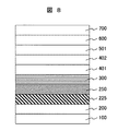
- a noble metal seed static stress driving layer 225 is newly provided.
- the lower electrode 100 is made of a Ru film and has a thickness of 50 nm.
- the seed layer 200 is composed of a Ta / Cu laminated film, and the film thickness is 5 nm.
- the noble metal seed static stress driving layer 225 is made of an Ag film and has a thickness of 5 nm.
- the dynamic stress driving layer 250 has a composition ratio of at. It is composed of an AuCu film at a ratio of approximately 50:50, and the film thickness is 10 nm.
- the film thickness of the L1 0 MnIr antiferromagnetic film 300 is 5 nm.
- the ferromagnetic film (1-a) 401 is composed of a Co film and has a thickness of 1.5 nm.
- the ferromagnetic film (1-b) 402 is composed of a half-metal CoMnSi film and has a thickness of 3 nm.
- the conductive nonmagnetic intermediate layer 501 is composed of a Cu—Al—O film and has a thickness of 2 nm.
- the ferromagnetic film (2) 600 is composed of a half-metal CoMnSi film and has a thickness of 3 nm.
- the upper electrode 700 is made of a Ru film and has a film thickness of 50 nm.
- the ferromagnetic film (1-a) 401 and the ferromagnetic film (1-b) 402 are firmly fixed by ferromagnetic / ferromagnetic exchange coupling.
- a new noble metal seed static stress driving layer is installed and added, so that even in the case of low-temperature heat treatment (350 ° C or lower) mentioned in 1, L1 0 MnIr about K e experimental values of the antiferromagnetic film 1.8erg / cm 2, T B value 600 ° C greater, and, even as a very small element size, the thermal fluctuation resistance of the astronomical numerical It becomes easier to obtain the value.
- the noble metal seed static stress driving layer according to the present embodiment may be composed of an Au film, an Au film, a Pt film, an Ir film, a Pd film, a Rh film, and an Ru film in addition to the Ag film. Furthermore, you may be comprised combining these metals of 2 elements or more.
- FIG. 8 shows a basic CPP-GMR structure of a noble metal seed static stress driving layer / AuCu or a PtMn based dynamic stress driving layer / L1 0 MnIr antiferromagnetic film, for example.
- a lower electrode 100 / seed layer 200 / noble metal seed static stress driving layer 2 may be sandwiched, for example.
- a dual structure type such as system dynamic stress driving layer 250 / noble metal seed static stress driving layer 225 / upper electrode 700 may be used.
- a laminated ferrimagnetic structure film made of, for example, NiFe / Ru / NiFe may be provided above the L1 0 MnIr antiferromagnetic film 300.
- the top laminated ferri structure film in the case of the dual structure type May be provided with a dual laminated ferri-structured film.
- the composition ratio of the AuCu dynamic stress driving layer and the PtMn dynamic stress driving layer Since the necessity of the seed layer when the additive element and the AuCu-based dynamic stress driving layer are used is the same as that of the second embodiment, the description thereof is omitted.
- a TMR element including a magnetic multilayer film in which a ferromagnetic film (1-b) 402, an insulating barrier layer 502, a ferromagnetic film (2) 600 serving as a free layer, and an upper electrode 700 are sequentially laminated.
- the opposite of the medium It shows an enlarged cross-sectional view as seen from the loose ABS surface.
- antiferromagnetic layer 300 for fixing layer is formed of L1 0 MnIr antiferromagnetic film, to promote the low-temperature ordering of the L1 0 MnIr antiferromagnetic film, AuCu, or PtMn-based dynamic stresses
- a noble metal seed static stress driving layer 225 is newly provided.
- the lower electrode 100 is made of a Ru film and has a thickness of 50 nm.
- the seed layer 200 is composed of a Ta / Cu laminated film, and the film thickness is 5 nm.
- the noble metal seed static stress driving layer 225 is made of an Ag film and has a thickness of 5 nm.
- the dynamic stress driving layer 250 has a composition ratio of at. It is composed of an AuCu film at a ratio of approximately 50:50, and the film thickness is 10 nm.
- the film thickness of the L1 0 MnIr antiferromagnetic film 300 is 5 nm.
- the ferromagnetic film (1-a) 401 is composed of a Co film and has a thickness of 1.5 nm.
- the ferromagnetic film (1-b) 402 is composed of a CoFeB film and has a thickness of 4 nm.
- the insulating barrier layer 502 is composed of an MgO film and has a thickness of 1.5 nm.
- the ferromagnetic film (2) 600 is composed of a CoFeB film and has a film thickness of 4 nm.
- the upper electrode 700 is made of a Ru film and has a film thickness of 50 nm.
- the ferromagnetic film (1-a) 401 and the ferromagnetic film (1-b) 402 are firmly fixed by ferromagnetic / ferromagnetic exchange coupling.
- a new noble metal seed static stress driving layer is installed and added, so that even in the case of low-temperature heat treatment (350 ° C or lower) mentioned in 1, L1 0 MnIr about K e experimental values of the antiferromagnetic film 1.8erg / cm 2, T B value 600 ° C greater, and, even as a very small element size, the thermal fluctuation resistance of the astronomical numerical It becomes easier to obtain the value.
- the noble metal seed static stress driving layer according to the present embodiment may be composed of an Au, Pt, Ir, Pd, Rh, or Ru film in addition to the Ag film. Furthermore, you may be comprised combining these metals of 2 elements or more.
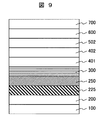
- FIG. 9 shows a basic TMR structure of a noble metal seed static stress driving layer / AuCu or a PtMn-based dynamic stress driving layer / L1 0 MnIr antiferromagnetic film.
- a laminated ferrimagnetic structure film made of, for example, NiFe / Ru / NiFe may be provided above the L1 0 MnIr antiferromagnetic film 300.
- the top laminated ferri structure film in the case of the dual structure type May be provided with a dual laminated ferri-structured film.
- the composition ratio of the AuCu dynamic stress driving layer and the PtMn dynamic stress driving layer Since the necessity of the seed layer when the additive element and the AuCu-based dynamic stress driving layer are used is the same as that of the second embodiment, the description thereof is omitted.
- the noble metal seed static stress driving layer 225 had an fcc crystal structure except for a Ru-based film.
- the Ru-based film had an hcp crystal structure.
- the noble metal seed static stress driving layer 225 exhibited (111) dense surface orientation except for the Ru-based film.
- the Ru-based film showed (001) plane dense surface orientation.
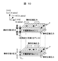
- FIG. 10 shows a schematic of static stress-driven MnIr low-temperature ordering using a noble metal seed according to the present embodiment.
- d 111 , d ⁇ 1-12 , and d ⁇ 110 are the (111) plane spacing, the ( ⁇ 1-12 ) plane spacing, and the ( ⁇ 110) plane spacing.
- a static stress driven MnIr low-temperature ordering mechanism in the case of using an Ag film as a noble metal seed static stress driving layer and a PtMn film as a dynamic stress driving layer will be described below.
- FIG. 11 shows a schematic of high-Ar pressure film-forming MnIr low-temperature ordering according to this example.
- d 111 is the (111) plane spacing.
- Example 2 and Example 3 dynamic stress-driven MnIr-based film low-temperature ordering with AuCu or PtMn-based film, static stress-driven MnIr-based film low-temperature ordering with noble metal seed, high Ar pressure production
- film-driven MnIr-based film low-temperature ordering has been described, it goes without saying that the combination of these three stress drives is the easiest to make MnIr-based film low-ordered.
- the most dominant of these three stress drives is dynamic stress-driven MnIr-based film low-temperature ordering with AuCu or PtMn-based films.
- FIG. 12 is a diagram showing an embodiment of a magnetic disk device (hard disk drive: HDD) using a CPP-GMR element or a TMR element according to the present invention.
- 1 is a diagram showing an outline in which a CPP-GMR element or TMR element according to the present invention is applied to an HDD.
- the CPP-GMR element or TMR element according to the present invention can be applied to, for example, a magnetic recording apparatus such as a magnetic tape apparatus, a magneto-optical disk apparatus, and a heat-assisted magnetic disk apparatus.
- the illustrated HDD includes a magnetic disk 10 as a magnetic recording medium formed in a disk shape for recording data in a recording area called a concentric track, and a CPP-GMR element or a TMR element according to the present invention.
- a magnetic head 18 for writing / reading the data an actuator 24 for supporting the magnetic head 18 and moving it to a predetermined position on the magnetic disk 10, and data to be written / read by the magnetic head 18 And a control means for controlling the movement of the actuator 24 and the like.
- At least one rotatable magnetic disk 10 is supported by a rotating shaft 12 and is rotated by a drive motor 14.
- At least one slider 16 is installed on the magnetic disk 10, and one or more sliders 16 are provided and support a magnetic head 18 for writing and reading information.
- the slider 16 moves on the surface of the magnetic disk 10 to access a predetermined position where data is recorded or a predetermined position where target data is recorded.
- the slider 16 is attached to the arm 22 by a gimbal 20.
- the gimbal 20 is given a slight elasticity, and the slider 16 is brought into close contact with the magnetic disk 10.
- the arm 22 is attached to the actuator 24.
- the actuator 24 there is a voice coil motor (hereinafter referred to as VCM).
- VCM voice coil motor
- the VCM is composed of a movable coil disposed in a fixed magnetic field, and the moving direction, moving speed, and the like of the coil are controlled by an electrical signal supplied from the control means 26 via the line 30. Therefore, the actuator 24 according to this embodiment includes the slider 16, the gimbal 20, the arm 22, the actuator 24, and the line 30.
- the rotation of the magnetic disk 10 causes an air bearing due to an air flow between the slider 16 and the surface of the magnetic disk 10, which causes the slider 16 to float from the surface of the magnetic disk 10. Therefore, during the operation of the magnetic disk device, this air bearing balances with the slight elasticity given to the gimbal 20, and the slider 16 does not touch the surface of the magnetic disk 10 and is constant with the magnetic disk 10. It is maintained to float at intervals.
- control means 26 includes a logic circuit, a memory, a microprocessor, and the like.
- the control means 26 transmits and receives control signals via each line and controls various constituent means of the magnetic disk device.
- the motor 14 is controlled by a motor drive signal transmitted via the line 28.
- the actuator 24 is controlled so as to move and position the slider 16 to the target data track on the magnetic disk 10 in accordance with a magnetic head position control signal and a seek control signal via the line 30.
- control means 26 transmits an electric signal for the magnetic head 18 to write as data on the magnetic disk 10 to the magnetic head 18 via the line 32. Further, the magnetic head 18 reads the data recorded on the magnetic disk 10 and receives the converted electric signal via the line 32 to decode it. That is, the control means 26 controls transmission / reception of electrical signals that the magnetic head 18 writes / reads.
- write / read signals may be transmitted directly from the magnetic head 18.
- control signal include an access control signal and a clock signal.
- the magnetic disk device may have a plurality of magnetic disks and actuators, and the actuator may have a plurality of magnetic heads.
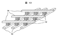
- FIG. 13 is a diagram showing an embodiment of a spin random access memory (SPRAM) using a TMR element according to the present invention. It is a figure which shows the outline which applied the TMR element concerning this invention to SPRAM. The schematic configuration of the SPRAM will be described below.
- SPRAM spin random access memory
- the illustrated SPRAM includes at least a plurality of lower fine lines 50, an upper fine line 54, and TMR elements 52 arranged at lattice points of the lower fine lines 50 and the upper fine lines 54.
- the lower fine line 50 is used as a gate electrode, and the upper fine line 54 is used as a bit line.
- the number of the lower fine lines 50 and the upper fine lines 54 arranged in the two-dimensional plane is the same.
- the lower fine line 50 is arranged on the substrate, and the upper fine line 54 is arranged above the lower fine line 50 so as to intersect the lower fine line 50.
- the TMR element 52 of any one of the first to third embodiments is arranged at a position between the lower fine line 50 and the upper fine line 54 at each intersecting position.
- the upper thin line 54 is made of, for example, a Cu film, and has a film thickness and a line width of 50 nm and 0.1 ⁇ m, respectively.
- the lower fine line 50 is also made of, for example, a Cu film, and has a film thickness and a line width of 50 nm and 0.1 ⁇ m, respectively.
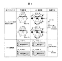
- FIG. 14 shows the directions of the magnetization vectors of the fixed layer and the free layer when “0” and “1” are recorded in the SPRAM. (A) is when the recording state is “0”, and (b) is when the recording state is “1”.
- the magnetization vectors of the fixed layer and the free layer are made antiparallel by so-called magnetization.
- the externally applied magnetic field becomes zero, but the pinned layer maintains the direction of the illustrated magnetization vector by exchange coupling with the adjacent antiferromagnetic film, and one free layer is owned by the free layer itself
- the direction of the illustrated magnetization vector is maintained by the induced magnetic anisotropy energy or the magnetocrystalline anisotropy energy.
- the recording state is “0”.
- the recording state is “1”.
- One reproduction is performed on the same principle as the TMR element. However, do not pass too much current. This is because, for example, the magnetization vector of the free layer in the recording state “0” causes the spin injection spin torque magnetization reversal, and the recording state “1” is changed. Therefore, regeneration must be performed while energizing a current equal to or lower than the threshold current described above.
- the recording state is “1”
- the magnetization vectors of the fixed layer and the free layer are in a parallel state, so that the TMR element has a low resistance.
- the recording state is “0”, since the magnetization vectors of the fixed layer and the free layer are in the antiparallel state, the TMR element has a high resistance. In the SPRAM, as described above, the recording state “1” is detected as low resistance, the recording state “0” is detected as high resistance, and reproduction is performed.
- the SPRAM shown in FIG. 13 is merely the application of the TMR element according to Embodiment 1-3 above to the current SPRAM, the effect of this is extremely great. As described above, even if the element size is extremely small, the anti-ferromagnetic film can be kept extremely resistant to thermal fluctuation. Therefore, it should be emphasized that it is easy to provide a super-integrated SPRAM by simply applying the TMR element according to Embodiment 1-3 to the SPRAM.
Landscapes
- Physics & Mathematics (AREA)
- Engineering & Computer Science (AREA)
- Chemical & Material Sciences (AREA)
- Condensed Matter Physics & Semiconductors (AREA)
- General Physics & Mathematics (AREA)
- Crystallography & Structural Chemistry (AREA)
- Nanotechnology (AREA)
- Manufacturing & Machinery (AREA)
- Power Engineering (AREA)
- Hall/Mr Elements (AREA)
- Mram Or Spin Memory Techniques (AREA)
- Magnetic Heads (AREA)
Abstract
現在、反強磁性膜として、不規則相Mn80Ir20膜、規則相Mn75Ir25膜が業界標準である。しかしながら、両者とも結晶構造が立方晶であるが故に結晶磁気異方性エネルギー定数が105erg/cm3程度と小であり、熱揺らぎ耐性が不足している状態にある。いわゆる、ピンデグレが顕在化している問題がある。 上記課題を克服するため、結晶磁気異方性エネルギー定数約2×10⁸erg/cm3を保有しているL10Mn50Ir50膜を固定層用、反強磁性膜300として適用する。これにより、例えば、素子サイズ5nm□、反強磁性膜厚5nmになっても、緩和時間1.2×1049年と、天文学的数値の熱揺らぎ耐性を確保できる。L10Mn50Ir50系反強磁性膜の低温規則化手段については、Mn50Ir50膜下方に動的応力駆動・静的応力駆動MnIr低温規則化層を設けることにより、解決する。
Description
本発明は、L10MnIr系反強磁性層を適用したCPP-GMR素子、TMR素子等の磁気抵抗効果素子、およびそれを用いた磁気記録再生装置〔ハードディスクドライブ(HDD)やスピンランダムアクセスメモリ(SPRAM)〕に関する。
高密度磁気記録再生対応の磁気センサとしてCPP-GMR(current perpendicular to the plane-Giant magnetoresistive)素子、TMR(Tunneling magnetoresistive)素子等の磁気抵抗効果素子が知られている。以下に、いわゆるスピンバルブタイプのCPP-GMR素子の概略、および、動作原理を説明する。
CPP-GMR素子は、導電性非磁性中間層によって分離された強磁性膜(1)と強磁性膜(2)を含む適切なる物質上に形成された積層構造を含有する。代表的なCPP-GMR素子構造は、下部電極/反強磁性層/強磁性膜(1)/導電性非磁性中間層/強磁性膜(2)/上部電極である。ここで、最上層が上部電極、最下層が下部電極であり、以下の積層膜もこのように表記する。強磁性膜のひとつ、強磁性膜(1)の磁化方向は、外部印加磁場ゼロのとき、強磁性膜(2)の磁化方向と垂直方向に固定されている。この強磁性膜(1)の磁化方向の固定は、反強磁性膜を隣接させ、反強磁性膜と強磁性膜(1)との交換結合により、強磁性膜(1)に一方向異方性エネルギー、或いは交換磁気異方性エネルギーを付与することによりなされる。そのため、強磁性膜(1)は、固定層、或いは固定側強磁性膜と呼ばれており、本明細書でも、このように表記する。固定層の代表的な磁化の固定方向は、媒体対抗面・浮上面(ABS面)と垂直な方向である。一方、強磁性膜(2)の磁化方向は、外部印加磁場によって自由に回転することができる。そのため、強磁性膜(2)は、自由層、或いは自由側強磁性膜と呼ばれており、本明細書でも、このように表記する。CPP-GMR素子では、磁性媒体から発生する磁場を印加磁場として、この磁場に応じて自由層の磁化方向が自由に回転し、結果、固定層の磁化方向と自由層の磁化方向とのなす角度に変化が生じる。CPP-GMR素子は、これら固定層と自由層の磁化方向のなす角度の変化に応じて電気抵抗が変化することを利用し、磁性媒体からの磁気的信号を電気的信号に変換する磁気抵抗トランスデューサーである。現在では、自由層や固定層に、いわゆるハーフメタル膜を使ったり、導電性非磁性中間層に電流狭窄と呼ばれている技術を導入したりして、MR比20%超が得られている。
一方の、TMR素子は、絶縁障壁層によって分離された強磁性膜(1)と強磁性膜(2)を含む適切なる物質上に形成された積層構造を含有する。代表的なTMR素子構造は、下部電極/反強磁性膜/強磁性膜(1)/絶縁障壁層/強磁性膜(2)/上部電極である。各々の膜の役割、および、TMR素子の動作原理は、絶縁障壁層を用いトンネル効果を利用して上下の通電をはかっている以外は、上で述べたCPP-GMR素子と同じである。現在、固定層、絶縁障壁層、自由層を、CoFeB/MgO/CoFeB構成とすることで、MR比350%超が得られている。
CPP-GMR素子、TMR素子ともに、高密度化・特性向上にあたっての要の技術は、固定層/導電性非磁性中間層、導電性非磁性中間層/自由層、および、固定層/絶縁障壁層、絶縁障壁層/自由層、の界面DOSの保有するスピン分極率を上げてのMR比を向上させる技術、そして、反強磁性層による固定層の強固なピンニング技術、いいかえると、固定層への大きな一方向異方性エネルギー、或いは交換磁気異方性エネルギー付与技術、と言っても過言ではない。
固定層用の反強磁性膜としては、不規則相FeMn膜、NiO膜、CrMnPt膜、L10PtMn膜、L10PtPdMn膜、不規則相MnIr膜、規則相Mn75Ir25膜、などが知られている。そして現在では、不規則相MnIr膜、規則相Mn75Ir25膜が業界標準として使用されている。ちなみに、規則相Mn75Ir25膜は、上記反強磁性膜の中では最も大きい交換磁気異方性エネルギー定数約1.3erg/cm2を付与できることで知られている。(特許文献1、非特許文献1、非特許文献2参照)
Appl. Phys. Lett., 89, 052504 (2006)
Appl. Phys. Lett., 85, 3812 (2004)
不規則相MnIr膜は、結晶構造が立方晶(fcc)であるが故に反強磁性膜の結晶磁気異方性エネルギー定数(KAF)が105erg/cm3のオーダにあり、小さい。同様に、規則相Mn75Ir25膜も、確かに巨大交換磁気異方性エネルギー定数(Ke)約1.3erg/cm2が得られるものの、やはり結晶構造がfccであるが故にKAFは105erg/cm3のオーダであり、小さい。
それゆえ、面記録密度Tb/in2超を達成するためには、CPP-GMR・TMR素子サイズを、例えば35□nm:トラック幅35nm、素子高さ35nmにまで低減することが必要とされているが、この素子サイズ、そして不規則相MnIr膜、或いは、規則相Mn75Ir25膜厚が5nmの場合について、(KAFVAF)/(kBT)値を計算してみると、もはや25を大きく下回っている。(VAF:反強磁性膜の体積、kB:ボルツマン定数、T:温度)。
(KAFVAF)/(kBT)<<25の場合について、反強磁性膜の結晶磁気異方性が維持される時間、いわゆる緩和時間τを、Neelの関係式τ=τ0exp[(KAFVAF)/(kBT)](τ0:Neelの定数)を用いて計算してみると、τ<<72sとなり、もはや、結晶磁気異方性は72sももたない、という数値がはじき出される。すなわち、熱揺らぎ耐性がまったくなく、固定層用の反強磁性膜として、まったく機能しないという問題に直面する。さらには、言うまでもなく、今後の記録密度向上に伴う素子サイズ低減の要求に耐えられない。
上記の問題を解決するため、本発明では、第一原理計算により予見されているKAF≒2×10⁸erg/cm3を保有する規則相L10MnIr膜(組成は、at.%比でおおよそ50:50。但し、組成マージンは広い。)を固定層用の反強磁性膜に適用する。具体的には以下のとおりである。
本発明の代表的なCPP-GMR素子は、少なくとも、下部電極上に、シード層と、反強磁性膜と、強磁性膜と、固定側強磁性層と、非磁性導電性中間層と、外部磁界に応じて磁化方向が自由に変化する自由側強磁性層と、上部電極とを有するCPP-GMR素子であって、
前記反強磁性膜が、結晶磁気異方性エネルギー定数を108erg/cm3以上保有するか、もしくは規則度を0.8以上保有するL10MnIr系反強磁性膜で構成されることを特徴とする。
また、本発明の代表的なTMR素子は、下部電極上に、シード層と、反強磁性膜と、強磁性膜と、固定側強磁性層と、絶縁性障壁層と、外部磁界に応じて磁化方向が自由に変化する自由側強磁性層と、上部電極とを有するTMR素子であって、
前記反強磁性膜が、結晶磁気異方性エネルギー定数を108erg/cm3以上保有するか、もしくは規則度を0.8以上保有するL10MnIr系反強磁性膜で構成されることを特徴とする。
但し、MnIr膜のL10規則相を得るためには、いいかえるとMnIr膜に不規則/規則相変態(規則化)を生じさせるためには、平衡状態図上、融点の約1/2である600゜C程度の高温熱処理、或いは、加熱しながらの形成が必要とされる。しかしながら、薄膜は非平衡状態にあり、種々の低温規則化技術を駆使して上で述べた温度を低減することが可能である。そこで本発明では、下記3つのMnIr膜の低温規則化の解決手段を提供する。
(1)AuCu系、PtMn系動的応力駆動MnIr膜低温規則化、
(2)貴金属シード配置による静的応力駆動MnIr膜低温規則化、
(3)そのほか、高Ar圧製膜駆動MnIr膜低温規則化。
本発明の代表的なCPP-GMR素子は、少なくとも、下部電極上に、シード層と、反強磁性膜と、強磁性膜と、固定側強磁性層と、非磁性導電性中間層と、外部磁界に応じて磁化方向が自由に変化する自由側強磁性層と、上部電極とを有するCPP-GMR素子であって、
前記反強磁性膜が、結晶磁気異方性エネルギー定数を108erg/cm3以上保有するか、もしくは規則度を0.8以上保有するL10MnIr系反強磁性膜で構成されることを特徴とする。
また、本発明の代表的なTMR素子は、下部電極上に、シード層と、反強磁性膜と、強磁性膜と、固定側強磁性層と、絶縁性障壁層と、外部磁界に応じて磁化方向が自由に変化する自由側強磁性層と、上部電極とを有するTMR素子であって、
前記反強磁性膜が、結晶磁気異方性エネルギー定数を108erg/cm3以上保有するか、もしくは規則度を0.8以上保有するL10MnIr系反強磁性膜で構成されることを特徴とする。
但し、MnIr膜のL10規則相を得るためには、いいかえるとMnIr膜に不規則/規則相変態(規則化)を生じさせるためには、平衡状態図上、融点の約1/2である600゜C程度の高温熱処理、或いは、加熱しながらの形成が必要とされる。しかしながら、薄膜は非平衡状態にあり、種々の低温規則化技術を駆使して上で述べた温度を低減することが可能である。そこで本発明では、下記3つのMnIr膜の低温規則化の解決手段を提供する。
(1)AuCu系、PtMn系動的応力駆動MnIr膜低温規則化、
(2)貴金属シード配置による静的応力駆動MnIr膜低温規則化、
(3)そのほか、高Ar圧製膜駆動MnIr膜低温規則化。
本発明によれば、超高密度に対応するため、素子サイズが極めて小さくなっても、極論するとCPP-GMR・TMR素子などの磁気抵抗効果素子終焉まで使える固定層用の反強磁性膜を提供できる。
例えば、素子サイズ10nm□、L10MnIr膜厚5nmのとき、(KAFVAF)/(kBT)値約2416、同様に、素子サイズ5nm□、L10MnIr膜厚5nmのとき、(KAFVAF)/(kBT)値約604、同様に、素子サイズ2.5nm□、L10MnIr膜厚5nmのとき、(KAFVAF)/(kBT)値約151と、熱揺らぎ耐性が極めて大きい固定層用の反強磁性膜を提供できる。
ちなみに、上で述べた(KAFVAF)/(kBT)=151から、τを計算してみると、τ=1.2×1049年と天文学的数値の熱揺らぎ耐性値が得られる。
例えば、素子サイズ10nm□、L10MnIr膜厚5nmのとき、(KAFVAF)/(kBT)値約2416、同様に、素子サイズ5nm□、L10MnIr膜厚5nmのとき、(KAFVAF)/(kBT)値約604、同様に、素子サイズ2.5nm□、L10MnIr膜厚5nmのとき、(KAFVAF)/(kBT)値約151と、熱揺らぎ耐性が極めて大きい固定層用の反強磁性膜を提供できる。
ちなみに、上で述べた(KAFVAF)/(kBT)=151から、τを計算してみると、τ=1.2×1049年と天文学的数値の熱揺らぎ耐性値が得られる。
以下、図面を参照して本発明の代表的な実施例について説明する。
<実施例1>
図1は、結晶磁気異方性エネルギー定数KAF=2×10⁸erg/cm3を保有するL10MnIr反強磁性膜を適用した、少なくとも、下部電極100上に、シード層200と、L10MnIr反強磁性膜300と、固定層の一部をなす強磁性膜(1-a)401と、固定層の一部をなす強磁性膜(固定側強磁性層)(1-b)402と、導電性非磁性中間層501と、自由層の役割を担う強磁性膜(自由側強磁性層)(2)600と、上部電極700と、を順次積層してなる磁性積層膜を含むCPP-GMR素子の媒体対抗面、いわゆるABS面から見た拡大断面図を示す。重複するが、固定層用の反強磁性膜300が、L10MnIr反強磁性膜で構成されることを特徴とする。
<実施例1>
図1は、結晶磁気異方性エネルギー定数KAF=2×10⁸erg/cm3を保有するL10MnIr反強磁性膜を適用した、少なくとも、下部電極100上に、シード層200と、L10MnIr反強磁性膜300と、固定層の一部をなす強磁性膜(1-a)401と、固定層の一部をなす強磁性膜(固定側強磁性層)(1-b)402と、導電性非磁性中間層501と、自由層の役割を担う強磁性膜(自由側強磁性層)(2)600と、上部電極700と、を順次積層してなる磁性積層膜を含むCPP-GMR素子の媒体対抗面、いわゆるABS面から見た拡大断面図を示す。重複するが、固定層用の反強磁性膜300が、L10MnIr反強磁性膜で構成されることを特徴とする。
実施例1のCPP-GMR素子の代表的な材料・膜厚は、以下のとおりである。下部電極100はRu膜で構成され、膜厚は50nmである。シード層200はTa/Cu積層膜で構成され、膜厚はともに5nmである。L10MnIr反強磁性膜300の膜厚は、5nmである。強磁性膜(1-a)401はCo膜で構成され、膜厚は1.5nmである。強磁性膜(1-b)402はハーフメタルCoMnSi膜で構成され、膜厚は3nmである。導電性非磁性中間層501はCu-Al-O膜で構成され、膜厚は2nmである。強磁性膜(2)600はハーフメタルCoMnSi膜で構成され、膜厚は3nmである。上部電極700はRu膜で構成され、膜厚は50nmである。なお、強磁性膜(1-a)401と強磁性膜(1-b)402とは、強磁性/強磁性の交換結合により強固に固定されている。
L10MnIr反強磁性膜にとって妥当な交換結合モデルであるMalozemoffモデル、Ke=4×z×π-3/2×√(AAF×KAF)(z:再隣接原子数、AAF:交換ステフィネス定数)、なる関係式を使ってKeの理論値をはじき出してみたところ、約80erg/cm2という値が得られた。この結果は、L10MnIr膜を固定層用の反強磁性膜として用いることにより、上で述べた固定層:強磁性膜(1-a)401/強磁性膜(1-b)402積層膜に、理想的には約80erg/cm2もの交換磁気異方性エネルギー定数を付与できることを示している。
しかしながら、実際には、格子不整合、界面汚染物質のコンタミ、膜中不純物、360゜面内異方性軸ローテーションがあり、上の理論値には届かない。
そこで、実際に、どの程度の交換磁気異方性エネルギー定数の実験値が得られるか、実験と計算により、以下に見積もってみた。
L10PtMn反強磁性膜は、L10MnIr反強磁性膜と結晶構造・磁気構造が類似していて、妥当交換結合モデルも同じMalozemoffモデルである、として知られる。そして、このL10PtMn反強磁性膜のKeの実験値は約0.4erg/cm2である。加えて、第一原理計算から予見されているL10PtMnのKAFは、L10MnIrの約1/20である。いいかえると、L10MnIrのKAFは、L10PtMnの約20倍である。以上の事実を、上のMalozemoffモデルからのKe〔=4×z×π-3/2×√(AAF×KAF)〕理論式にはめこんで比例計算を行うと、L10MnIr反強磁性膜のKeの実験値は、Ke≒0.4(erg/cm2)×√20(倍)≒1.8erg/cm2、という値が得られる。なお、L10MnIr、L10PtMnのzはともに12と同じであり、AAFについてもネール温度(TN)や再隣接Mn原子間距離等がほとんど同じであることから、zやAAFについては、各々、1倍、約1倍として見積もった。
以上、L10MnIr膜を固定層用の反強磁性膜として用いることにより、実験的にも、固定層:強磁性膜(1-a)401/強磁性膜(1-b)402積層膜に、Ke約1.8erg/cm2もの極めて大きな交換磁気異方性エネルギー定数を付与できることが分かった。なお、このKe約1.8erg/cm2は、これまでに知られている規則相Mn75Ir25反強磁性膜の約1.3erg/cm2を凌ぐ値である。
L10MnIr反磁性膜のブロッキング温度TBについては、L10MnIrのTNが約867゜Cもあることから、極めて高く、膜が壊れてしまって測定困難である。しかしながら、結晶構造・磁気構造が類似していて、妥当交換結合モデルも同じであるL10PtMn、L10NiMn反強磁性膜のTBがTNよりもおおよそ200゜C低い温度にある、ことの類推から、TB約600゜C超と見積もられる。
次に、本発明のキーである熱揺らぎ耐性について、以下に述べたい。熱揺らぎ耐性を示す物理パラメータは、(KAFVAF)/(kBT)値、および、τ=τ0exp[(KAFVAF)/(kBT)]である。L10MnIr反磁性膜のKAF=2×108erg/cm3を用いて、代表的な素子サイズについて計算すると、以下のとおり見積もられる。
例えば、素子サイズ10nm□、L10MnIr膜厚5nmのとき、(KAFVAF)/(kBT)値約2416、同様に、素子サイズ5nm□、L10MnIr膜厚5nmのとき、(KAFVAF)/(kBT)値約604、同様に、素子サイズ2.5nm□、L10MnIr膜厚5nmのとき、(KAFVAF)/(kBT)値約151と、熱揺らぎ耐性が極めて高いことが分かる。ちなみに、上で述べた(KAFVAF)/(kBT)値約151から、τを計算してみると、τ=1.2×1049yearsと天文学的数値の熱揺らぎ耐性値が得られる。噛み砕いて言うならば、L10MnIr反強磁性膜の異方性軸が倒れるまでには、1.2×1049yearsもの年数がかかる。以上から、L10MnIr膜を固定層用の反強磁性膜として用いることにより、素子サイズが極めて小さくなっても、極論すると、CPP-GMR・TMR素子などの磁気抵抗効果素子終焉まで使える固定層用の反強磁性膜を提供できる。
以上の熱揺らぎ耐性は、L10MnIr反強磁性膜のKAFが約2×10⁸erg/cm3であって規則度Sが約1の場合であるが、実際には規則度S=1を得ることは難しい。規則度Sは、0.8程度まで落ちてしまう場合が多い。しかしながら、規則度Sは0.8以上もあれば十分である。なぜなら、規則度Sが0.8に下がった場合には、KAFは1/2くらいまで減少するとされているが、KAF=1×108erg/cm3まで減少したとしても、素子サイズ小としても上記天文学的数値の熱揺らぎ耐性値が維持されるからである。すなわち、素子サイズ2.5nm□、L10MnIr膜厚5nmとしてもτ=2.1×1014yearsと天文学的数値の熱揺らぎ耐性値が維持される。したがって、L10MnIr反強磁性膜のKAFは108erg/cm3のオーダを保有していれば十分であり、規則度Sも0.8以上もあれば十分である。
なお、KAF=1×10⁸erg/cm3の場合、理屈上、Ke=1.2erg/cm2まで減少するが、Ke値としては0.4erg/cm2以上あれば実用上問題ないが故にこの低下は問題なく、一方のTB値は、一番良好な交換結合手で決まるが故に600°C超は維持されることを付記しておきたい。
なお、本発明に係わる、L10MnIr反強磁性膜の組成は、上でも述べたとおり、at.%比でおおよそ50:50であるが、組成マージンが広いため多少ずれていても構わない。加えて、Pt、Pd、Rh、Au、Ag、Ruなど数at.%~数10at.%添加しても良く、これら2元素以上の貴金属を組み合わせて添加しても良い。
さらに、図1では、L10MnIr反強磁性膜下置きタイプの基本的なCPP-GMR構造を示したが、L10MnIr反強磁性膜上置きタイプとしても良く、さらにはサンドイッチしてデュアル構造タイプとしても良い。
さらに、L10MnIr反強磁性膜300の下方に、例えば、不規則相MnIr/NiFe/Ru/NiFeで構成される積層フェリ構造膜を設けても構わない。同様に、上置き積層フェリ構造膜、デユアル積層フェリ構造膜を設けても、良い。
さらに、図1では、良質なハーフメタルCoMnSi膜〔強磁性膜(1-b)〕を得るため、Co膜〔強磁性膜(1-a)〕を介在させたが、必要に応じ、強磁性膜(1-a)はなくても構わない。
図2に、結晶磁気異方性エネルギー定数KAF=2×10⁸erg/cm3を保有するL10MnIr反強磁性膜を適用した、少なくとも、下部電極100上に、シード層200と、L10MnIr反強磁性膜300と、固定層の一部をなす強磁性膜(1-a)401と、固定層の一部をなす強磁性膜(1-b)402と、絶縁障壁層502と、自由層の役割を担う強磁性膜(2)600と、上部電極700と、を順次積層してなる磁性積層膜を含むTMR素子の媒体対抗面、いわゆるABS面から見た拡大断面図を示す。重複するが、固定層用の反強磁性膜300が、L10MnIr反強磁性膜で構成されることを特徴とする。
実施例1のTMR素子の代表的な材料・膜厚は、以下のとおりである。下部電極100はRu膜で構成され、膜厚は50nmである。シード層200はTa/Cu積層膜で構成され、膜厚はともに5nmである。L10MnIr反強磁性膜300の膜厚は、5nmである。強磁性膜(1-a)401はCo膜で構成され、膜厚は1.5nmである。強磁性膜(1-b)402はCoFeB膜で構成され、膜厚は4nmである。絶縁障壁層502はMgO膜で構成され、膜厚は1.5nmである。強磁性膜(2)600はCoFeB膜で構成され、膜厚は4nmである。上部電極700はRu膜で構成され、膜厚は50nmである。なお、強磁性膜(1-a)401と強磁性膜(1-b)402とは、強磁性/強磁性の交換結合により強固に固定されている。
本TMR素子構造でも、L10MnIr反強磁性膜を固定層用の反強磁性膜に用いることにより、上で述べた、Ke実験値約1.8erg/cm2、TB値600°C超、そして、素子サイズを極めて小としても、天文学的数値の熱揺らぎ耐性値が得られる。
なお、上でも述べたとおり、実際にはL10MnIr反強磁性膜のKAF=2×10⁸erg/cm3、規則度S≒1を得ることは難しい。規則度Sは、0.8程度まで落ちてしまう場合が多い。しかしながら、規則度Sは0.8以上もあれば十分である。なぜなら、規則度Sが0.8に下がった場合には、KAFは1/2くらいまで減少するとされているが、KAF=1×108erg/cm3まで減少したとしても、素子サイズ小としても天文学的数値の熱揺らぎ耐性値が維持されるからである。すなわち、素子サイズ2.5nm□、L10MnIr膜厚5nmとしてもτ=2.1×1014yearsと天文学的数値の熱揺らぎ耐性値が維持される。したがって、L10MnIr反強磁性膜のKAFは108erg/cm3のオーダを保有していれば十分であり、規則度Sも0.8以上もあれば十分である。
なお、KAF=1×10⁸erg/cm3の場合、理屈上、Ke=1.2erg/cm2まで減少するが、Ke値としては0.4erg/cm2以上あれば実用上問題ないが故にこの低下は問題なく、一方のTB値は、一番良好な交換結合手で決まるが故に600°C超は維持されることを付記しておきたい。
なお、本発明に係わる、L10MnIr反強磁性膜の組成は、上でも述べたとおり、at.%比でおおよそ50:50であるが、組成マージンが広いため多少ずれていても構わない。加えて、Pt、Pd、Rh、Au、Ag、Ruなど数at.%~数10at.%添加しても良く、これら2元素以上の貴金属を組み合わせて添加しても良い。
さらに、図2では、L10MnIr反強磁性膜下置きタイプの基本的なTMR構造を示したが、L10MnIr反強磁性膜上置きタイプとしても良く、さらにはサンドイッチしてデュアル構造タイプとしても良い。
さらに、L10MnIr反強磁性膜300の上方に、例えば、NiFe/Ru/NiFeで構成される積層フェリ構造膜を設けても構わない。同様に、L10MnIr反強磁性膜上置きタイプの場合には上置き積層フェリ構造膜、デュアル構造タイプの場合にはデュアル積層フェリ構造膜を設けても、良い。
さらに、図2では、良質なCoFeB膜〔強磁性膜(1-b)402〕を得るため、Co膜〔強磁性膜(1-a)401〕を介在させたが、必要に応じ、強磁性膜(1-a)はなくても構わない。
<実施例2>
図3は、結晶磁気異方性エネルギー定数KAF=2×10⁸erg/cm3を保有するL10MnIr反強磁性膜を適用した、そして動的応力駆動MnIr低温規則化を図るためにAuCu、或いはPtMn系動的応力駆動層を新たに設けた、少なくとも、下部電極100上に、シード層200と、AuCu、或いはPtMn系動的応力駆動層250と、L10MnIr反強磁性膜300と、固定層の一部をなす強磁性膜(1-a)401と、固定層の一部をなす強磁性膜(1-b)402と、導電性非磁性中間層501と、自由層の役割を担う強磁性膜(2)600と、上部電極700と、を順次積層してなる磁性積層膜を含むCPP-GMR素子の媒体対抗面、いわゆるABS面から見た拡大断面図を示す。重複するが、固定層用の反強磁性膜300が、L10MnIr反強磁性膜で構成され、その上で、L10MnIr反強磁性膜の低温規則化を促進するためにAuCu、或いはPtMn系動的応力駆動層250が設けられていることを特徴とする。
図3は、結晶磁気異方性エネルギー定数KAF=2×10⁸erg/cm3を保有するL10MnIr反強磁性膜を適用した、そして動的応力駆動MnIr低温規則化を図るためにAuCu、或いはPtMn系動的応力駆動層を新たに設けた、少なくとも、下部電極100上に、シード層200と、AuCu、或いはPtMn系動的応力駆動層250と、L10MnIr反強磁性膜300と、固定層の一部をなす強磁性膜(1-a)401と、固定層の一部をなす強磁性膜(1-b)402と、導電性非磁性中間層501と、自由層の役割を担う強磁性膜(2)600と、上部電極700と、を順次積層してなる磁性積層膜を含むCPP-GMR素子の媒体対抗面、いわゆるABS面から見た拡大断面図を示す。重複するが、固定層用の反強磁性膜300が、L10MnIr反強磁性膜で構成され、その上で、L10MnIr反強磁性膜の低温規則化を促進するためにAuCu、或いはPtMn系動的応力駆動層250が設けられていることを特徴とする。
実施例2のCPP-GMR素子の代表的な材料・膜厚は、以下のとおりである。下部電極100はRu膜で構成され、膜厚は50nmである。シード層200はTa/Cu積層膜で構成され、膜厚はともに5nmである。動的応力駆動層250は組成比がat.%比でおおよそ50:50にあるAuCu膜で構成され、膜厚は10nmである。L10MnIr反強磁性膜300の膜厚は、5nmである。強磁性膜(1-a)401はCo膜で構成され、膜厚は1.5nmである。強磁性膜(1-b)402はハーフメタルCoMnSi膜で構成され、膜厚は3nmである。導電性非磁性中間層501はCu-Al-O膜で構成され、膜厚は2nmである。強磁性膜(2)600はハーフメタルCoMnSi膜で構成され、膜厚は3nmである。上部電極700はRu膜で構成され、膜厚は50nmである。なお、強磁性膜(1-a)401と強磁性膜(1-b)402とは、強磁性/強磁性の交換結合により強固に固定されている。
上記AuCu、或いはPtMn系動的応力駆動層を設けることにより、低温熱処理(350°C以下)で、実施例1で述べた、L10MnIr反強磁性膜のKe実験値約1.8erg/cm2、TB値600°C超、そして、素子サイズを極めて小としても、天文学的数値の熱揺らぎ耐性値が得られやすくなる。
なお、本実施例に係わる、AuCu動的応力駆動層の組成は、上でも述べたとおり、at.%比でおおよそ50:50であるが、組成マージンが広いため多少ずれていても構わない。加えて、Pt、Pd、Rh、Ir、Ag、Ru、や、Fe、Co、Niなど数at.%添加されていても構わない。さらには、これら2元素以上の金属を組み合わせて添加していても良い。
本実施例に係わる、PtMn動的応力駆動層の組成については、at.%比でおおよそ50:50であるが、組成マージンが広いため多少ずれていても構わない。加えて、Au、Pd、Rh、Ir、Ag、Ru、や、Fe、Co、Niなど数at.%添加されていても構わない。さらには、これら2元素以上の金属を組み合わせて添加しても良い。
さらに、AuCu系動的応力駆動層を用いた場合には、シード層200はなくても構わない。なぜなら、AuCu系膜は、シード層がなくても良好な稠密面(111)配向を示すからである。
さらに、図3では、AuCu、或いはPtMn系動的応力駆動層/L10MnIr反強磁性膜の下置きタイプの基本的なCPP-GMR構造を示したが、例えば、下部電極100/シード層200/強磁性膜(2)600/導電性非磁性中間層501/強磁性膜(1-b)402/強磁性膜(1-a)401/L10MnIr反強磁性膜300/AuCu、或いはPtMn系動的応力駆動層250/上部電極700、のようにL10MnIr反強磁性膜/AuCu、或いはPtMn系動的応力駆動層の上置きタイプとしても良く、さらには、サンドイッチして、例えば、下部電極100/シード層200/AuCu、或いはPtMn系動的応力駆動層250/L10MnIr反強磁性膜300/強磁性膜(1-a)401/強磁性膜(1-b)402/導電性非磁性中間層501/強磁性膜(2)600/導電性非磁性中間層501/強磁性膜(1-b)402/強磁性膜(1-a)401/L10MnIr反強磁性膜300/AuCu、或いはPtMn系動的応力駆動層250/上部電極700、のようにデュアル構造タイプとしても良い。
さらに、L10MnIr反強磁性膜300の上方に、例えば、NiFe/Ru/NiFeで構成される積層フェリ構造膜を設けても構わない。同様に、L10MnIr反強磁性膜/AuCu、或いはPtMn系動的応力駆動層の上置きタイプの場合には上置き積層フェリ構造膜、デュアル構造タイプの場合にはデュアル積層フェリ構造膜を設けても、良い。
L10MnIr反強磁性膜の添加元素、強磁性膜(1-a)401の要否論については、実施例1と同じのため、説明を省略する。
図4は、結晶磁気異方性エネルギー定数KAF=2×10⁸erg/cm3を保有するL10MnIr反強磁性膜を適用した、そして動的応力駆動MnIr低温規則化を図るためにAuCu、或いはPtMn系動的応力駆動層を新たに設けた、少なくとも、下部電極100上に、シード層200と、AuCu、或いはPtMn系動的応力駆動層250と、L10MnIr反強磁性膜300と、固定層の一部をなす強磁性膜(1-a)401と、固定層の一部をなす強磁性膜(1-b)402と、絶縁障壁層502と、自由層の役割を担う強磁性膜(2)600と、上部電極700と、を順次積層してなる磁性積層膜を含むTMR素子の媒体対抗面、いわゆるABS面から見た拡大断面図を示す。重複するが、固定層用の反強磁性膜300が、L10MnIr反強磁性膜で構成され、その上で、L10MnIr反強磁性膜の低温規則化を促進するためにAuCu、或いはPtMn系動的応力駆動層250が設けられていることを特徴とする。
実施例2のTMR素子の代表的な材料・膜厚は、以下のとおりである。下部電極100はRu膜で構成され、膜厚は50nmである。シード層200はTa/Cu積層膜で構成され、膜厚はともに5nmである。動的応力駆動層250は組成比がat.%比でおおよそ50:50にあるAuCu膜で構成され、膜厚は10nmである。L10MnIr反強磁性膜300の膜厚は、5nmである。強磁性膜(1-a)401はCo膜で構成され、膜厚は1.5nmである。強磁性膜(1-b)402はCoFeB膜で構成され、膜厚は4nmである。絶縁障壁層502はMgO膜で構成され、膜厚は1.5nmである。強磁性膜(2)600はCoFeB膜で構成され、膜厚は4nmである。上部電極700はRu膜で構成され、膜厚は50nmである。なお、強磁性膜(1-a)401と強磁性膜(1-b)402とは、強磁性/強磁性の交換結合により強固に固定されている。
上記AuCu、或いはPtMn系動的応力駆動層を設けることにより、低温熱処理(350°C以下)で、実施例1で述べた、L10MnIr反強磁性膜のKe実験値約1.8erg/cm2、TB値600°C超、そして、素子サイズを極めて小としても、天文学的数値の熱揺らぎ耐性値が得られやすくなる。
なお、本実施例に係わる、AuCu動的応力駆動層の組成は、上でも述べたとおり、at.%比でおおよそ50:50であるが、組成マージンが広いため多少ずれていても構わない。加えて、Pt、Pd、Rh、Ir、Ag、Ru、や、Fe、Co、Niなど数at.%添加されていても構わない。さらには、これら2元素以上の金属を組み合わせて添加していても良い。
本実施例に係わる、PtMn動的応力駆動層の組成については、at.%比でおおよそ50:50であるが、組成マージンが広いため多少ずれていても構わない。加えて、Au、Pd、Rh、Ir、Ag、Ru、や、Fe、Co、Niなど数at.%添加されていても構わない。さらには、これら2元素以上の金属を組み合わせて添加しても良い。
さらに、AuCu系動的応力駆動層を用いた場合には、シード層はなくても構わない。なぜなら、AuCu系膜は、シード層がなくても良好な稠密面(111)配向を示すからである。
さらに、図4では、AuCu、或いはPtMn系動的応力駆動層/L10MnIr反強磁性膜の下置きタイプの基本的なTMR構造を示したが、例えば、下部電極100/シード層200/強磁性膜(2)600/絶縁障壁層502/強磁性膜(1-b)402/強磁性膜(1-a)401/L10MnIr反強磁性膜300/AuCu、或いはPtMn系動的応力駆動層250/上部電極700、のようにL10MnIr反強磁性膜/AuCu、或いはPtMn系動的応力駆動層の上置きタイプとしても良く、さらには、サンドイッチして、例えば、下部電極100/シード層200/AuCu、或いはPtMn系動的応力駆動層250/L10MnIr反強磁性膜300/強磁性膜(1-a)401/強磁性膜(1-b)402/絶縁障壁層502/強磁性膜(2)600/絶縁障壁層502/強磁性膜(1-b)402/強磁性膜(1-a)401/L10MnIr反強磁性膜300/AuCu、或いはPtMn系動的応力駆動層250/上部電極700、のようにデュアル構造タイプとしても良い。
さらに、L10MnIr反強磁性膜300の上方に、例えば、NiFe/Ru/NiFeで構成される積層フェリ構造膜を設けても構わない。同様に、L10MnIr反強磁性膜/AuCu、或いはPtMn系動的応力駆動層の上置きタイプの場合には上置き積層フェリ構造膜、デュアル構造タイプの場合にはデュアル積層フェリ構造膜を設けても、良い。
L10MnIr反強磁性膜の添加元素、強磁性膜(1-a)401の要否論については、実施例1と同じのため、説明を省略する。
上記実施例に係わる、AuCu、或いはPtMn系膜、および、MnIr系膜の結晶構造は、ともに、不規則相ではfcc、規則相では面心正方晶(fct)である。そして、AuCu、PtMn、および、MnIr系膜は、不規則相状態にあっても、規則相状態にあっても、ともに(111)配向を示していた。
そこで、図5に、上記実施例に係わる、AuCu膜、および、MnIr膜の(111)面内、および、(111)面間の格子パラメータを示す。AuCu膜、MnIr膜とも、規則化に伴い、(111)面稠密六方格子の2辺:(-110)面間隔(d-110)が長くなり、残り4辺、いいかえると、(-1-12)面間隔(d-1-12)が短くなっているのが分かる。すなわち、[-1-12]方向に自発歪み(圧縮)、[-110]方向に自発歪み(引張り)、が生じて規則化する。なお、d111は、(111)面間隔である。
同様に、図6に、上記実施例に係わる、PtMn膜、および、MnIr膜の(111)面内、および、(111)面間の格子パラメータを示す。PtMn膜、MnIr膜とも、規則化に伴い、(111)面稠密六方格子の2辺:(-110)面間隔(d-110)が長くなり、残り4辺、いいかえると、(-1-12)面間隔(d-1-12)が短くなっているのが分かる。加えて、(111)面間隔(d111)が短くなっているのが分かる。すなわち、[111]、[-1-12]方向に自発歪み(圧縮)、[-110]方向に自発歪み(引張り)、が生じて規則化する。以上のように自発歪みを伴う不規則/規則相変態は、広義の意味でマルテンサイト変態と称されている。
図5、6を踏まえ、上記実施例に係わる、3方向動的応力駆動MnIr低温規則化について、以下に説明する。図7は、上記実施例に係わる、3方向動的応力駆動MnIr低温規則化のSchematicである。AuCu膜も同じであるが、ここでは、話を分かりやすくするためPtMn動的応力駆動MnIr低温規則化のメカニズムについて以下に記載する。図中、d111、d-1-12、および、d-110は、(111)面間隔、(-1-12)面間隔、および、(-110)面間隔である。
PtMn膜の規則化温度は約250-275°Cと低い。そのため、熱処理を行うと、まずはじめにPtMn[111]、[-1-12]方向に自発歪み(圧縮)、[-110]方向に自発歪み(引張り)が生じる(図6参照)、次いで、これら、自発歪は、上方のMnIr膜に、MnIr[111]、[-1-12]方向動的引張り応力、MnIr[-110]方向動的圧縮応力を付与する。最後に、これら動的応力が、熱処理中に、MnIr膜のMnIr[111]、[-1-12]方向自発歪み(圧縮)、MnIr[-110]方向自発歪み(引張り)(図6参照)をアシストする。それゆえ、MnIr膜規則化のための相互拡散活性化エネルギーの山を越えやすくなって、MnIr膜の低温規則化が促進される、という訳である。
AuCu動的応力駆動MnIr低温規則化も、AuCu膜の規則化温度が275-325°C程度と低いが故に上記とほぼ同じメカニズムである。ただ、AuCu膜の場合には、熱処理に伴うAuCu[111]方向の自発歪みはほとんどない(図5参照)。しかしながら、AuCu膜規則化の際のAuCu[-110]方向自発歪み(引張り)は、極めて大きい。それゆえ熱処理を行うと、まずはじめに上側のMnIr膜に、実効的にMnIr[111]方向動的引張り応力が付与され、次いで、この動的応力がMnIr[111]方向自発歪み(圧縮)をアシストしている、ということは、おおいに考えられうることである。噛み砕いて述べるならば、AuCu動的応力駆動層を用いても、PtMn動的応力駆動層と同様、MnIr[111]方向にも動的応力駆動が働く。
以上のように、PtMn動的応力駆動層、AuCu動的応力駆動層を用いることにより、3方向動的応力駆動:MnIr[111]、[-1-12]方向動的引張り応力駆動、MnIr[-110]方向動的圧縮応力駆動、が働いて、MnIr低温規則化が促進される。
上記、3方向動的応力駆動MnIr低温規則化をスムーズに働かせるためには、図5、6から分かるように、AuCu、或いは、PtMn系動的応力駆動層と、L10MnIr系反強磁性膜との格子パラメータ長さ関係を、AuCu、或いはPtMn系膜、および、MnIr系膜の不規則/規則相変態前後で、下記(1)-(7)を満足させる必要がある:
(1)不規則相AuCu、或いはPtMn系膜の(-110)面間隔>不規則相MnIr系膜の(-110)面間隔、
(2)不規則相AuCu、或いはPtMn系膜の(-110)面間隔<規則相AuCu、或いはPtMn系膜の(-110)面間隔、
(3)不規則相AuCu、或いはPtMn系膜の(-1-12)面間隔>規則相AuCu、或いはPtMn系膜の(-1-12)面間隔、
(4)不規則相MnIr系膜の(-110)面間隔<規則相MnIr系膜の(-110)面間隔、
(5)不規則相MnIr系膜の(-1-12)面間隔>規則相MnIr系膜の(-1-12)面間隔、
(6)不規則相AuCu、或いはPtMn系膜の(111)面間隔≒規則相AuCu、或いはPtMn系膜の(111)面間隔、もしくは、不規則相AuCu、或いはPtMn系膜の(111)面間隔>規則相AuCu、或いはPtMn系膜の(111)面間隔、
(7)不規則相MnIr系膜の(111)面間隔>規則相MnIr系膜の(111)面間隔、
を満足させる必要がある。
(1)不規則相AuCu、或いはPtMn系膜の(-110)面間隔>不規則相MnIr系膜の(-110)面間隔、
(2)不規則相AuCu、或いはPtMn系膜の(-110)面間隔<規則相AuCu、或いはPtMn系膜の(-110)面間隔、
(3)不規則相AuCu、或いはPtMn系膜の(-1-12)面間隔>規則相AuCu、或いはPtMn系膜の(-1-12)面間隔、
(4)不規則相MnIr系膜の(-110)面間隔<規則相MnIr系膜の(-110)面間隔、
(5)不規則相MnIr系膜の(-1-12)面間隔>規則相MnIr系膜の(-1-12)面間隔、
(6)不規則相AuCu、或いはPtMn系膜の(111)面間隔≒規則相AuCu、或いはPtMn系膜の(111)面間隔、もしくは、不規則相AuCu、或いはPtMn系膜の(111)面間隔>規則相AuCu、或いはPtMn系膜の(111)面間隔、
(7)不規則相MnIr系膜の(111)面間隔>規則相MnIr系膜の(111)面間隔、
を満足させる必要がある。
これら大小関係がひとつでも逆転した場合には、例えば、上記(2)の大小関係が逆転した場合には、MnIr膜にはMnIr[-110]方向動的引張り応力が付与されてしまい、結果、3方向動的応力駆動:MnIr[111]、[-1-12]方向動的引張り応力駆動、MnIr[-110]方向動的圧縮応力駆動、のうちのMnIr[-110]方向動的圧縮応力駆動が失われて、MnIr膜低温規則化が困難な事態に陥る。
<実施例3>
図8は、結晶磁気異方性エネルギー定数KAF=2×10⁸erg/cm3を保有するL10MnIr反強磁性膜を適用し、AuCu、或いはPtMn系動的応力駆動層を設けた上で、さらに、静的応力駆動MnIr低温規則化を図るために新たに貴金属シード静的応力駆動層を設けた、少なくとも、下部電極100上に、シード層200と、貴金属シード静的応力駆動層225と、AuCu、或いはPtMn系動的応力駆動層250と、L10MnIr反強磁性膜300と、固定層の一部をなす強磁性膜(1-a)401と、固定層の一部をなす強磁性膜(1-b)402と、導電性非磁性中間層501と、自由層の役割を担う強磁性膜(2)600と、上部電極700と、を順次積層してなる磁性積層膜を含むCPP-GMR素子の媒体対抗面、いわゆるABS面から見た拡大断面図を示す。重複するが、固定層用の反強磁性膜300がL10MnIr反強磁性膜で構成され、そのL10MnIr反強磁性膜の低温規則化を促進するため、AuCu、或いはPtMn系動的応力駆動層250に加えて、新たに貴金属シード静的応力駆動層225を設けたことを特徴とする。
図8は、結晶磁気異方性エネルギー定数KAF=2×10⁸erg/cm3を保有するL10MnIr反強磁性膜を適用し、AuCu、或いはPtMn系動的応力駆動層を設けた上で、さらに、静的応力駆動MnIr低温規則化を図るために新たに貴金属シード静的応力駆動層を設けた、少なくとも、下部電極100上に、シード層200と、貴金属シード静的応力駆動層225と、AuCu、或いはPtMn系動的応力駆動層250と、L10MnIr反強磁性膜300と、固定層の一部をなす強磁性膜(1-a)401と、固定層の一部をなす強磁性膜(1-b)402と、導電性非磁性中間層501と、自由層の役割を担う強磁性膜(2)600と、上部電極700と、を順次積層してなる磁性積層膜を含むCPP-GMR素子の媒体対抗面、いわゆるABS面から見た拡大断面図を示す。重複するが、固定層用の反強磁性膜300がL10MnIr反強磁性膜で構成され、そのL10MnIr反強磁性膜の低温規則化を促進するため、AuCu、或いはPtMn系動的応力駆動層250に加えて、新たに貴金属シード静的応力駆動層225を設けたことを特徴とする。
実施例3のCPP-GMR素子の代表的な材料・膜厚は、以下のとおりである。下部電極100はRu膜で構成され、膜厚は50nmである。シード層200はTa/Cu積層膜で構成され、膜厚はともに5nmである。貴金属シード静的応力駆動層225はAg膜で構成され、膜厚は5nmである。動的応力駆動層250は組成比がat.%比でおおよそ50:50にあるAuCu膜で構成され、膜厚は10nmである。L10MnIr反強磁性膜300の膜厚は、5nmである。強磁性膜(1-a)401はCo膜で構成され、膜厚は1.5nmである。強磁性膜(1-b)402はハーフメタルCoMnSi膜で構成され、膜厚は3nmである。導電性非磁性中間層501はCu-Al-O膜で構成され、膜厚は2nmである。強磁性膜(2)600はハーフメタルCoMnSi膜で構成され、膜厚は3nmである。上部電極700はRu膜で構成され、膜厚は50nmである。なお、強磁性膜(1-a)401と強磁性膜(1-b)402とは、強磁性/強磁性の交換結合により強固に固定されている。
上記のように、AuCu、或いはPtMn系動的応力駆動層に加え、新たに貴金属シード静的応力駆動層を設置・加算することにより、低温熱処理(350°C以下)であっても、実施例1で述べた、L10MnIr反強磁性膜のKe実験値約1.8erg/cm2、TB値600°C超、そして、素子サイズを極めて小としても、天文学的数値の熱揺らぎ耐性値が、より一層得られやすくなる。
なお、本実施例に係わる、貴金属シード静的応力駆動層は、Ag膜のほか、Au、Pt、Ir、Pd、Rh、および、Ru膜で構成されていても良い。さらには、これら2元素以上の金属を組み合わせて構成されていても構わない。
さらに、図8では、貴金属シード静的応力駆動層/AuCu、或いはPtMn系動的応力駆動層/L10MnIr反強磁性膜の下置きタイプの基本的なCPP-GMR構造を示したが、例えば、下部電極100/シード層200/強磁性膜(2)600/導電性非磁性中間層501/強磁性膜(1-b)402/強磁性膜(1-a)401/L10MnIr反強磁性膜300/AuCu、或いはPtMn系動的応力駆動層250/貴金属シード静的応力駆動層225/上部電極700、のようにL10MnIr反強磁性膜/AuCu、或いはPtMn系動的応力駆動層/貴金属シード静的応力駆動層の上置きタイプとしても良く、さらには、サンドイッチして、例えば、下部電極100/シード層200/貴金属シード静的応力駆動層225/AuCu、或いはPtMn系動的応力駆動層250/L10MnIr反強磁性膜300/強磁性膜(1-a)401/強磁性膜(1-b)402/導電性非磁性中間層501/強磁性膜(2)600/導電性非磁性中間層501/強磁性膜(1-b)402/強磁性膜(1-a)401/L10MnIr反強磁性膜300/AuCu、或いはPtMn系動的応力駆動層250/貴金属シード静的応力駆動層225/上部電極700、のようにデュアル構造タイプとしても良い。
さらに、L10MnIr反強磁性膜300の上方に、例えば、NiFe/Ru/NiFeで構成される積層フェリ構造膜を設けても構わない。同様に、L10MnIr反強磁性膜/AuCu、或いはPtMn系動的応力駆動層/貴金属シード静的応力駆動層の上置きタイプの場合には上置き積層フェリ構造膜、デュアル構造タイプの場合にはデュアル積層フェリ構造膜を設けても、良い。
L10MnIr反強磁性膜の添加元素、強磁性膜(1-a)の要否論については、実施例1と同じのため、AuCu動的応力駆動層、PtMn動的応力駆動層の組成比と添加元素、AuCu系動的応力駆動層を用いた場合のシード層の要否論については、実施例2と同じため、説明を省略する。
図9は、結晶磁気異方性エネルギー定数KAF=2×10⁸erg/cm3を保有するL10MnIr反強磁性膜を適用し、AuCu、或いはPtMn系動的応力駆動層を設けた上で、さらに、静的応力駆動MnIr低温規則化を図るために新たに貴金属シード静的応力駆動層を設けた、少なくとも、下部電極100上に、シード層200と、貴金属シード静的応力駆動層225と、AuCu、或いはPtMn系動的応力駆動層250と、L10MnIr反強磁性膜300と、固定層の一部をなす強磁性膜(1-a)401と、固定層の一部をなす強磁性膜(1-b)402と、絶縁障壁層502と、自由層の役割を担う強磁性膜(2)600と、上部電極700と、を順次積層してなる磁性積層膜を含むTMR素子の媒体対抗面、いわゆるABS面から見た拡大断面図を示す。重複するが、固定層用の反強磁性膜300がL10MnIr反強磁性膜で構成され、そのL10MnIr反強磁性膜の低温規則化を促進するため、AuCu、或いはPtMn系動的応力駆動層250に加えて、新たに貴金属シード静的応力駆動層225を設けたことを特徴とする。
実施例3のTMR素子の代表的な材料・膜厚は、以下のとおりである。下部電極100はRu膜で構成され、膜厚は50nmである。シード層200はTa/Cu積層膜で構成され、膜厚はともに5nmである。貴金属シード静的応力駆動層225はAg膜で構成され、膜厚は5nmである。動的応力駆動層250は組成比がat.%比でおおよそ50:50にあるAuCu膜で構成され、膜厚は10nmである。L10MnIr反強磁性膜300の膜厚は、5nmである。強磁性膜(1-a)401はCo膜で構成され、膜厚は1.5nmである。強磁性膜(1-b)402はCoFeB膜で構成され、膜厚は4nmである。絶縁障壁層502はMgO膜で構成され、膜厚は1.5nmである。強磁性膜(2)600はCoFeB膜で構成され、膜厚は4nmである。上部電極700はRu膜で構成され、膜厚は50nmである。なお、強磁性膜(1-a)401と強磁性膜(1-b)402とは、強磁性/強磁性の交換結合により強固に固定されている。
上記のように、AuCu、或いはPtMn系動的応力駆動層に加え、新たに貴金属シード静的応力駆動層を設置・加算することにより、低温熱処理(350°C以下)であっても、実施例1で述べた、L10MnIr反強磁性膜のKe実験値約1.8erg/cm2、TB値600°C超、そして、素子サイズを極めて小としても、天文学的数値の熱揺らぎ耐性値が、より一層得られやすくなる。
なお、本実施例に係わる、貴金属シード静的応力駆動層は、Ag膜のほか、Au、Pt、Ir、Pd、Rh、又はRu膜で構成されていても良い。さらには、これら2元素以上の金属を組み合わせて構成されていても構わない。
さらに、図9では、貴金属シード静的応力駆動層/AuCu、或いはPtMn系動的応力駆動層/L10MnIr反強磁性膜の下置きタイプの基本的なTMR構造を示したが、例えば、下部電極100/シード層200/強磁性膜(2)600/絶縁障壁層502/強磁性膜(1-b)402/強磁性膜(1-a)401/L10MnIr反強磁性膜300/AuCu、或いはPtMn系動的応力駆動層250/貴金属シード静的応力駆動層225/上部電極700、のようにL10MnIr反強磁性膜/AuCu、或いはPtMn系動的応力駆動層/貴金属シード静的応力駆動層の上置きタイプとしても良く、さらには、サンドイッチして、例えば、下部電極100/シード層200/貴金属シード静的応力駆動層225/AuCu、或いはPtMn系動的応力駆動層250/L10MnIr反強磁性膜300/強磁性膜(1-a)401/強磁性膜(1-b)402/絶縁障壁層502/強磁性膜(2)600/絶縁障壁層502/強磁性膜(1-b)402/強磁性膜(1-a)401/L10MnIr反強磁性膜300/AuCu、或いはPtMn系動的応力駆動層250/貴金属シード静的応力駆動層225/上部電極700、のようにデュアル構造タイプとしても良い。
さらに、L10MnIr反強磁性膜300の上方に、例えば、NiFe/Ru/NiFeで構成される積層フェリ構造膜を設けても構わない。同様に、L10MnIr反強磁性膜/AuCu、或いはPtMn系動的応力駆動層/貴金属シード静的応力駆動層の上置きタイプの場合には上置き積層フェリ構造膜、デュアル構造タイプの場合にはデュアル積層フェリ構造膜を設けても、良い。
L10MnIr反強磁性膜の添加元素、強磁性膜(1-a)の要否論については、実施例1と同じのため、AuCu動的応力駆動層、PtMn動的応力駆動層の組成比と添加元素、AuCu系動的応力駆動層を用いた場合のシード層の要否論については、実施例2と同じため、説明を省略する。
本実施例に係わる、貴金属シード静的応力駆動層225は、Ru系膜を除き、fccの結晶構造を保有していた。Ru系膜については、hcpの結晶構造であった。そして、貴金属シード静的応力駆動層225は、Ru系膜を除き、(111)稠密面配向を示していた。Ru系膜については、(001)面稠密面配向を示していた。
そこで、図10に、本実施例に係わる、貴金属シードによる静的応力駆動MnIr低温規則化のSchematicを示す。図中、d111、d-1-12、および、d-110は、(111)面間隔、(-1-12)面間隔、および、(-110)面間隔である。例として、貴金属シード静的応力駆動層としてAg膜、動的応力駆動層としてPtMn膜を用いた場合についての、静的応力駆動MnIr低温規則化のメカニズムを以下に記載する。
まずはじめに、この静的応力駆動を働かせるためには、下記の前提条件が必要とされる。すなわち、PtMn膜、MnIr膜が不規則相状態にあるとき、Ag膜と、PtMn膜と、MnIr膜の(111)面稠密六方格子の一辺の長さ関係が、或いは、格子定数の長さ関係が、Ag膜>PtMn膜>MnIr膜、にあることが必要とされる。なぜならこの静的応力は、Ag(111)/不規則相PtMn(111)の大きな格子ミスマッチに起因し、不規則相PtMn膜を介して、不規則相MnIr膜に付与されるMnIr[111]方向静的引張り応力だからである。貴金属シード静的応力駆動層としてAg膜、動的応力駆動層としてPtMn膜、反強磁性膜としてMnIr膜を選択した場合には、稠密六方格子の一辺の長さ関係は、Ag(2.892オングストローム)>不規則相PtMn(2.761オングストローム)>不規則相MnIr(2.696オングストローム)であり、上記の長さ関係を満たす。
図10に示すように、この長さ関係があるがために、As-dep.状態、そしてPtMn膜、MnIr膜が不規則相状態にあるとき、不規則相MnIr膜にMnIr[111]方向の静的引張り応力が、不規則相PtMn膜を介して付与される。次いで、この静的応力が、熱処理中、MnIr膜のMnIr[111]方向の自発歪み(圧縮)(図6参照)をアシストする。それゆえ、MnIr膜規則化のための相互拡散活性化エネルギーの山を越えやすくなって、MnIr膜の低温規則化が促進される、という訳である。
動的応力駆動層としてPtMn膜の代わりにAuCu膜を用いた場合にも、稠密六方格子の一辺の長さ関係は、Ag(2.892オングストローム)>不規則相AuCu(2.744オングストローム)>不規則相MnIr(2.696オングストローム)にあり、上で述べた長さ関係を満たす。それゆえ、AuCu膜を用いた場合にも、図10と同じメカニズムでもって静的応力駆動MnIr低温規則化が促進される。
貴金属シードとしてすでに述べた代替材料を適用する場合には、そしてAuCu、或いはPtMn膜、および、MnIr膜にすでに述べた添加元素をドープする場合には、これら貴金属シード、AuCu、或いはPtMn系膜、MnIr系膜の稠密面六方格子の一辺の長さ関係が、貴金属シード>不規則相AuCu、或いはPtMn系膜>不規則相MnIr系膜、を満たすよう代替材料、添加元素、添加量を選択する必要がある、ということは言うまでもない。本関係を満たせない場合には、貴金属シード静的応力駆動MnIr低温規則化は働かない。
そのほか、静的応力駆動として、高Ar圧製膜駆動MnIr低温規則化がある。図11に、本実施例に係わる、高Ar圧製膜駆動MnIr低温規則化のSchematicを示す。図中、d111は、(111)面間隔である。例として、貴金属シード静的応力駆動層としてAg膜、動的応力駆動層としてPtMn膜を用いた場合についての、高Ar圧製膜駆動MnIr低温規則化のメカニズムを以下に記載する。
まず、As-dep.段階で、Ag膜、PtMn膜、MnIr膜のすべての膜に静的引張り応力を付与できるよう、適当な高Ar圧値、例えば10mTorrでスパッタ形成する。言うまでもなく、これにより、不規則相MnIr膜にはMnIr[111]方向の静的引張り応力が付与される。次いで、この静的応力が、熱処理中、MnIr膜のMnIr[111]方向の自発歪み(圧縮)(図6参照)をアシストする。それゆえ、MnIr膜規則化のための相互拡散活性化エネルギーの山を越えやすくなって、MnIr膜の低温規則化が促進される、という訳である。
重複するかもしれないが、この高Ar圧製膜駆動MnIr系膜低温規則化を働かせるためには、貴金属シード静的応力駆動層、AuCu、或いはPtMn系膜動的応力駆動層、そしてMnIr系膜に、As-dep.段階で静的引張り応力を付与できるよう、各々の膜・層にとって十分に高いAr圧値を見出して、スパッタ形成する必要がある。
以上、実施例2、および、実施例3にて、AuCu、或いはPtMn系膜による動的応力駆動MnIr系膜低温規則化、貴金属シードによる静的応力駆動MnIr系膜低温規則化、高Ar圧製膜駆動MnIr系膜低温規則化を述べてきたが、これら3つの応力駆動を組み合わせた場合が、最もMnIr系膜を低温規則化させやすい、ということは言うまでもない。加えて、これら3つの応力駆動の中で最もdominantなのは、AuCu、或いはPtMn系膜による動的応力駆動MnIr系膜低温規則化であることを付記しておきたい。
最後に、サイクル熱処理、すなわち2回目以降の熱処理を行った場合には、新たに2種類の静的応力駆動MnIr系膜低温規則化:(1)L10AuCu、或いはL10PtMn系膜(111)/MnIr系膜(111)格子ミスマッチ起因のMnIr系膜[111]方向静的応力駆動MnIr系膜低温規則化、(2)貴金属シード(111)/L10AuCu、或いはL10PtMn系膜(111)格子ミスマッチ起因のMnIr系膜[111]方向静的応力駆動MnIr系膜低温規則化、が加算され、サイクル熱処理、2回目以降の熱処理を行うことにより、MnIr系膜の規則度Sを向上させやすくなる、ことを付記しておきたい。
<実施例4>
図12は、本発明に係わる、CPP-GMR素子、或いはTMR素子を用いた磁気ディスク装置(ハードディスクドライブ:HDD)についての一実施例を示す図である。HDDに本発明に係わるCPP-GMR素子、或いはTMR素子を適用した概略を示す図である。しかしながら、本発明に係わるCPP-GMR素子、或いはTMR素子は、たとえば、磁気テープ装置などのような磁気記録装置、光磁気ディスク装置、熱アシスト磁気ディスク装置にも適用することが可能である。
図12は、本発明に係わる、CPP-GMR素子、或いはTMR素子を用いた磁気ディスク装置(ハードディスクドライブ:HDD)についての一実施例を示す図である。HDDに本発明に係わるCPP-GMR素子、或いはTMR素子を適用した概略を示す図である。しかしながら、本発明に係わるCPP-GMR素子、或いはTMR素子は、たとえば、磁気テープ装置などのような磁気記録装置、光磁気ディスク装置、熱アシスト磁気ディスク装置にも適用することが可能である。
図示したHDDは、同心円状のトラックと呼ばれる記録領域にデータを記録するためのディスク状に形成された磁気記録媒体としての磁気ディスク10と、本発明に係わるCPP-GMR素子、或いはTMR素子を含む、上記データの書き込み・読み取りを行うための磁気ヘッド18と、この磁気ヘッド18を支え、そして磁気ディスク10上の所定の位置へ移動させるためのアクチュエータ24と、磁気ヘッド18が書き込み・読み取りするデータの送受信、および、アクチュエータ24の移動などを制御する制御手段と、を含み構成される。
構成と動作について、以下に説明する。少なくとも一枚の回転可能な磁気ディスク10が回転軸12により支持されており、駆動用モータ14により回転させられる。少なくとも一個のスライダ16が、磁気ディスク10上に設置され、このスライダ16は、一個以上設けられており、情報を書き込み・読み込むための磁気ヘッド18を支持している。
磁気ディスク10が回転すると同時に、スライダ16が磁気ディスク10表面を移動することにより、データを記録する所定位置にアクセス、或いは、目的とするデータが記録されている所定位置にアクセスされる。スライダ16は、ジンバル20によってアーム22に取り付けられる。ジンバル20にはわずかな弾力性を付与し、スライダ16を磁気ディスク10に密着させる。アーム22は、アクチュエータ24に取り付けられる。
アクチュエータ24としては、ボイスコイルモータ(以下、VCMと呼ぶ)がある。VCMは固定された磁界中に配置された移動可能なコイルから構成され、コイルの移動方向、および、移動速度等は、制御手段26からライン30を介して与えられる電気信号により制御される。したがって、本実施例によるアクチュエータ24は、スライダ16とジンバル20とアーム22とアクチュエータ24とライン30を含み構成される。
磁気ディスクの動作中、磁気ディスク10の回転によりスライダ16と磁気ディスク10表面との間に空気流によるエアベアリングが生じ、それがスライダ16を磁気ディスク10の表面から浮上させる。よって、磁気ディスク装置動作中には、このエアベアリングはジンバル20に付与されているわずかな弾力性とバランスを取り、スライダ16は磁気ディスク10表面に触れずに、かつ、磁気ディスク10と一定の間隔を保って浮上するよう維持される。
通常、制御手段26は、ロジック回路、メモリ、および、マイクロプロセッサなどから構成される。そして制御手段26は、各ラインを介して制御信号を送受信し、かつ、磁気ディスク装置の種々の構成手段を制御する。
例えば、モータ14は、ライン28を介し伝達されるモータ駆動信号により制御される。アクチュエータ24は、ライン30を介した磁気ヘッド位置の制御信号、および、シーク制御信号等により、磁気ディスク10上の目的とするデータトラックにスライダ16を最適位置に移動、位置決めするよう制御される。
そして、制御手段26は、磁気ヘッド18が磁気ディスク10にデータとして書き込むための電気信号を、ライン32を介して、磁気ヘッド18に送信する。また、磁気ヘッド18が磁気ディスク10に記録されたデータを読み取り、変換した電気信号を、ライン32を介して受信し、解読する。すなわち、制御手段26は、磁気ヘッド18が、書き込み・読み取りする電気信号の送受信を制御している。
なお、上記の書き込み・読み取り信号は、磁気ヘッド18から直接伝達される手段も可能である。また、制御信号として、例えばアクセス制御信号、および、クロック信号などがある。さらに、磁気ディスク装置には、複数の磁気ディスクやアクチュエータ等を保有し、そのアクチュエータが複数の磁気ヘッドを保有していてもよい。
図12に示すHDDは、本発明に係わる、CPP-GMR素子、或いは、TMR素子を現状HDDに適用しただけではあるが、これによる効果は極めて大きい。すでに述べたとおり、素子サイズを極めて小としても、反強磁性膜の熱揺らぎ耐性極めて大を維持できる。したがって、本発明に係わる、CPP-GMR素子、もしくはTMR素子をHDDに適用するだけで、超高密度対応HDDを提供しやすくなる、ということを強調しておきたい。
図13は、本発明に係わる、TMR素子を用いたスピンランダムアクセスメモリ(SPRAM)についての一実施例を示す図である。SPRAMに本発明に係わるTMR素子を適用した概略を示す図である。以下に、そのSPRAMの概略構成を述べる。
図示したSPRAMは、少なくとも、複数の下部細線50と、上部細線54と、下部細線50と上部細線54との格子点に配置されたTMR素子52とを含み構成される。下部細線50はゲート電極として、上部細線54はビット線として使用される。2次元面内に配列された下部細線50と上部細線54の本数は同じである。
例えば、基板上に、下部細線50が配置され、その上方に、上部細線54が、下部細線50と交差するよう配置される。そして各々の交差する位置にあって、下部細線50と上部細線54とに挟まれる位置に、上記実施例1~3のいずれかのTMR素子52を配置して構成される。上部細線54は、例えばCu膜で構成され、膜厚、線幅はそれぞれ50nm、0.1μmである。下部細線50も、例えばCu膜で構成され、膜厚、線幅はそれぞれ50nm、0.1μmである。
次に、SPRAMの動作原理について、簡単に触れておく。SPRAMでは、例えば、下記のようにして記録が行われる。図14に、そのSPRAMへの「0」「1」記録状態時の固定層と自由層の磁化ベクトルの方向を示す。(a)は記録状態「0」にあるとき、(b)は記録状態「1」にあるときである。
図14(a)に示すように、初期状態では、いわゆる着磁により固定層と自由層の磁化ベクトルを反平行状態にさせておく。着磁後、外部印加磁場はゼロとなってしまうが、固定層は隣接する反強磁性膜との交換結合により図示した磁化ベクトルの方向が維持され、一方の自由層は自由層自身の保有する誘導磁気異方性エネルギー、もしくは結晶磁気異方性エネルギーにより図示した磁化ベクトルの方向が維持される。SPRAMでは、このように固定層と自由層の磁化ベクトルが反平行状態にあるとき、例えば、記録状態「0」にあるとする。
この状態から、例えば、図14(b)に示すパルス電流iを流す。これにより、自由層の異方性エネルギーが弱いがためにある一定の電流値、これを閾値電流と呼ぶが、この閾値以上の電流を流すことにより自由層の磁化ベクトルは、いわゆるスピン注入スピントルク磁化反転を起こし、まずはじめにパルス電流iと平行方向に向けられ、次いで、自由層のもうひとつの異方性軸(磁化安定軸)、すなわち初期状態とは反対方向に向けられ、落ち着く。SPRAMでは、以上のように記録を行って、固定層と自由層の磁化ベクトルの方向が平行状態にあるとき、例えば、記録状態「1」にあるとする。
一方の再生は、TMR素子と同じ原理にて行う。但し、あまり大きな電流を流してはいけない。なぜなら、例えば記録状態「0」にある自由層の磁化ベクトルがスピン注入スピントルク磁化反転を起こしてしまい、記録状態「1」に転じてしまうからである。よって、再生は、上で述べた閾値電流以下の電流を通電しながら行わなければならない。記録状態「1」にあるとき、固定層と自由層の磁化ベクトルは平行状態にあるが故にTMR素子は低抵抗になる。一方、記録状態「0」にあるときは、固定層と自由層の磁化ベクトルは反平行状態にあるが故にTMR素子は高抵抗になる。SPRAMでは、以上のように、記録状態「1」を低抵抗であるとして検知、記録状態「0」を高抵抗であるとして検知し、再生を行う。
最後に、図13に示すSPRAMは、上記実施例1-3に係わる、TMR素子を現状SPRAMに適用しただけではあるが、これによる効果は極めて大きい。すでに述べたとおり、素子サイズを極めて小としても、反強磁性膜の熱揺らぎ耐性極めて大を維持できる。したがって、上記実施例1-3に係わる、TMR素子をSPRAMに適用するだけで、超集積度対応SPRAMを提供しやすくなる、ということを強調しておきたい。
10…磁気ディスク、12…回転軸、14…モータ、16…スライダ、18…磁気ヘッド、20…ジンバル、22…アーム、24…アクチュエータ、26…制御手段、50…下部細線、52…スピン注入スピントルク磁化反転型TMR素子、54…上部細線、100…下部電極、200…シード層、225…貴金属シード静的応力駆動層、250…動的応力駆動層、300…L10MnIr系反強磁性膜、401…強磁性膜(1-a)、402…強磁性膜(1-b)、501…導電性非磁性中間層、502…絶縁障壁層、600…強磁性膜(2)、700…上部電極。
Claims (12)
- 少なくとも、下部電極上に、シード層と、反強磁性膜と、強磁性膜と、固定側強磁性層と、非磁性導電性中間層と、外部磁界に応じて磁化方向が自由に変化する自由側強磁性層と、上部電極とを有するCPP-GMR素子であって、
前記反強磁性膜が、結晶磁気異方性エネルギー定数を108erg/cm3以上保有するか、もしくは規則度を0.8以上保有するL10MnIr系反強磁性膜で構成されることを特徴とするCPP-GMR素子。 - 請求項1記載のCPP-GMR素子において、前記L10MnIr系反強磁性膜の下方に該L10MnIr系反強磁性膜の低温規則化を図るためのAuCu或いはPtMn系動的応力駆動層を設けたことを特徴とするCPP-GMR素子。
- 請求項2記載のCPP-GMR素子において、前記AuCu或いはPtMn系動的応力駆動層の下方に、前記L10MnIr系反強磁性膜の低温規則化を図るための貴金属シード静的応力駆動層を設けたことを特徴とするCPP-GMR素子。
- 請求項3記載のCPP-GMR素子において、前記貴金属シード静的応力駆動層と、前記AuCu或いはPtMn系動的応力駆動層と、前記L10MnIr系反強磁性膜との稠密六方格子の一辺の長さ関係、或いは格子定数の長さ関係が、前記AuCu或いはPtMn系動的応力駆動層、および前記L10MnIr系反強磁性膜が不規則相状態にあるとき、貴金属シード静的応力駆動層>不規則相AuCu或いはPtMn系膜>不規則相MnIr系膜の関係にあることを特徴とするCPP-GMR素子。
- 請求項2記載のCPP-GMR素子において、前記AuCu或いはPtMn系動的応力駆動層と、前記L10MnIr系反強磁性膜との格子パラメータの長さ関係が、AuCu或いはPtMn系膜およびMnIr系膜の不規則/規則相変態前後で、
不規則相AuCu或いはPtMn系膜の(-110)面間隔<規則相AuCu或いはPtMn系膜の(-110)面間隔、
不規則相AuCu或いはPtMn系膜の(-1-12)面間隔>規則相AuCu或いはPtMn系膜の(-1-12)面間隔、
不規則相MnIr系膜の(-110)面間隔<規則相MnIr系膜の(-110)面間隔、および、
不規則相MnIr系膜の(-1-12)面間隔>規則相MnIr系膜の(-1-12)面間隔、
の関係にあることを特徴とするCPP-GMR素子。 - 少なくとも、下部電極上に、シード層と、反強磁性膜と、強磁性膜と、固定側強磁性層と、絶縁性障壁層と、外部磁界に応じて磁化方向が自由に変化する自由側強磁性層と、上部電極とを有するTMR素子であって、
前記反強磁性膜が、結晶磁気異方性エネルギー定数を108erg/cm3以上保有するか、もしくは規則度を0.8以上保有するL10MnIr系反強磁性膜で構成されることを特徴とするTMR素子。 - 請求項6記載のTMR素子において、前記L10MnIr系反強磁性膜の下方に該L10MnIr系強磁性膜の低温規則化を図るためのAuCu或いはPtMn系動的応力駆動層を設けたことを特徴とするTMR素子。
- 請求項7記載のTMR素子において、前記AuCu或いはPtMn系動的応力駆動層の下方に、前記L10MnIr系反強磁性層の低温規則化を図るための貴金属シード静的応力駆動層を設けたことを特徴とするTMR素子。
- 請求項8記載のTMR素子において、前記貴金属シード静的応力駆動層と、前記AuCu或いはPtMn系動的応力駆動層と、前記L10MnIr系反強磁性膜との稠密六方格子の一辺の長さ関係、或いは格子定数の長さ関係が、前記AuCu或いはPtMn系動的応力駆動層、および前記L10MnIr系反強磁性膜が不規則相状態にあるとき、貴金属シード静的応力駆動層>不規則相AuCu或いはPtMn系膜>不規則相MnIr系膜の関係にあることを特徴とするTMR素子。
- 請求項7記載のTMR素子において、前記AuCu或いはPtMn系動的応力駆動層と、前記L10MnIr系反強磁性膜との格子パラメータの長さ関係が、AuCu或いはPtMn系膜およびMnIr系膜の不規則/規則相変態前後で、
不規則相AuCu或いはPtMn系膜の(-110)面間隔<規則相AuCu或いはPtMn系膜の(-110)面間隔、
不規則相AuCu或いはPtMn系膜の(-1-12)面間隔>規則相AuCu或いはPtMn系膜の(-1-12)面間隔、
不規則相MnIr系膜の(-110)面間隔<規則相MnIr系膜の(-110)面間隔、および、
不規則相MnIr系膜の(-1-12)面間隔>規則相MnIr系膜の(-1-12)面間隔、
の関係にあることを特徴とするTMR素子。 - 情報を記録する磁気記録媒体と、
前記情報を書き込みする記録ヘッドと、前記情報を読み取る、請求項1乃至5のいずれかに記載のCPP-GMR素子、或いは請求項6乃至10のいずれに記載のTMR素子を有する再生ヘッドを含む磁気ヘッドと、
前記磁気ヘッドを前記磁気記録媒体上の所定の位置へ移動させるアクチュエータと、
前記磁気ヘッドが読み取りまたは書き込みする前記情報の送受信と前記アクチュエータの移動を制御する制御手段と、
を有することを特徴とする磁気記録再生装置。 - 少なくとも、基板上に、複数の下部細線が配置され、その上方に、該下部細線と同数の上部細線が、該下部細線と交差するよう配置され、該下部細線と該上部細線の交差する位置にあって、該下部細線と該上部細線とに挟まれる位置に、請求項6乃至10のいずれかに記載のTMR素子が配置されることを特徴とするスピンランダムアクセスメモリ。
Applications Claiming Priority (2)
| Application Number | Priority Date | Filing Date | Title |
|---|---|---|---|
| JP2008-281596 | 2008-10-31 | ||
| JP2008281596A JP2012033515A (ja) | 2008-10-31 | 2008-10-31 | Cpp−gmr素子、tmr素子および磁気記録再生装置。 |
Publications (1)
| Publication Number | Publication Date |
|---|---|
| WO2010050125A1 true WO2010050125A1 (ja) | 2010-05-06 |
Family
ID=42128498
Family Applications (1)
| Application Number | Title | Priority Date | Filing Date |
|---|---|---|---|
| PCT/JP2009/005183 Ceased WO2010050125A1 (ja) | 2008-10-31 | 2009-10-06 | Cpp-gmr素子、tmr素子および磁気記録再生装置 |
Country Status (2)
| Country | Link |
|---|---|
| JP (1) | JP2012033515A (ja) |
| WO (1) | WO2010050125A1 (ja) |
Cited By (1)
| Publication number | Priority date | Publication date | Assignee | Title |
|---|---|---|---|---|
| WO2014063412A1 (zh) * | 2012-10-26 | 2014-05-01 | 苏州大学 | 基于磁温差电效应的传感器元件及其实现方法 |
Families Citing this family (1)
| Publication number | Priority date | Publication date | Assignee | Title |
|---|---|---|---|---|
| CN111033778B (zh) * | 2017-09-27 | 2023-12-19 | 阿尔卑斯阿尔派株式会社 | 交换耦合膜以及使用该交换耦合膜的磁阻效应元件及磁检测装置 |
Citations (6)
| Publication number | Priority date | Publication date | Assignee | Title |
|---|---|---|---|---|
| JP2000332318A (ja) * | 1998-06-30 | 2000-11-30 | Toshiba Corp | 磁気抵抗効果素子、磁気ヘッド、磁気ヘッドアセンブリ及び磁気記録装置 |
| JP2002026421A (ja) * | 2000-06-30 | 2002-01-25 | Toshiba Corp | 磁気抵抗効果素子の製造方法と強磁性トンネル接合素子 |
| JP2004186659A (ja) * | 2002-10-07 | 2004-07-02 | Alps Electric Co Ltd | 磁気検出素子 |
| WO2005008799A1 (ja) * | 2003-07-18 | 2005-01-27 | Fujitsu Limited | Cpp磁気抵抗効果素子及びその製造方法、磁気ヘッド、磁気記憶装置 |
| JP2005333106A (ja) * | 2004-04-20 | 2005-12-02 | Ken Takahashi | 交換結合素子とその製造方法並びに交換結合素子を具備したデバイス |
| JP2007251013A (ja) * | 2006-03-17 | 2007-09-27 | Tdk Corp | 磁気抵抗効果素子、薄膜磁気ヘッド、磁気ヘッド装置及び磁気記録再生装置 |
-
2008
- 2008-10-31 JP JP2008281596A patent/JP2012033515A/ja active Pending
-
2009
- 2009-10-06 WO PCT/JP2009/005183 patent/WO2010050125A1/ja not_active Ceased
Patent Citations (6)
| Publication number | Priority date | Publication date | Assignee | Title |
|---|---|---|---|---|
| JP2000332318A (ja) * | 1998-06-30 | 2000-11-30 | Toshiba Corp | 磁気抵抗効果素子、磁気ヘッド、磁気ヘッドアセンブリ及び磁気記録装置 |
| JP2002026421A (ja) * | 2000-06-30 | 2002-01-25 | Toshiba Corp | 磁気抵抗効果素子の製造方法と強磁性トンネル接合素子 |
| JP2004186659A (ja) * | 2002-10-07 | 2004-07-02 | Alps Electric Co Ltd | 磁気検出素子 |
| WO2005008799A1 (ja) * | 2003-07-18 | 2005-01-27 | Fujitsu Limited | Cpp磁気抵抗効果素子及びその製造方法、磁気ヘッド、磁気記憶装置 |
| JP2005333106A (ja) * | 2004-04-20 | 2005-12-02 | Ken Takahashi | 交換結合素子とその製造方法並びに交換結合素子を具備したデバイス |
| JP2007251013A (ja) * | 2006-03-17 | 2007-09-27 | Tdk Corp | 磁気抵抗効果素子、薄膜磁気ヘッド、磁気ヘッド装置及び磁気記録再生装置 |
Cited By (2)
| Publication number | Priority date | Publication date | Assignee | Title |
|---|---|---|---|---|
| WO2014063412A1 (zh) * | 2012-10-26 | 2014-05-01 | 苏州大学 | 基于磁温差电效应的传感器元件及其实现方法 |
| US9797962B2 (en) | 2012-10-26 | 2017-10-24 | Soochow University | Sensor element based on magneto-thermoelectric effect, and realizing method thereof |
Also Published As
| Publication number | Publication date |
|---|---|
| JP2012033515A (ja) | 2012-02-16 |
Similar Documents
| Publication | Publication Date | Title |
|---|---|---|
| US8213129B2 (en) | Current-perpendicular-to-plane magnetoresistive element in which the magnetization direction of an intermediate metallic magnetic layer is twisted | |
| JP5018982B2 (ja) | スペーサ層を含むcpp型磁気抵抗効果素子 | |
| CN100435372C (zh) | 沉积有氧化物磁性层和金属磁性膜的磁致电阻元件 | |
| US7505235B2 (en) | Method and apparatus for providing magnetostriction control in a freelayer of a magnetic memory device | |
| CN101640098B (zh) | 磁性薄膜及其成膜方法以及磁性薄膜的应用装置 | |
| Tannous et al. | Magnetic information-storage materials | |
| JPWO2009054062A1 (ja) | サンドイッチ構造の磁化自由層を有する磁気トンネル接合素子 | |
| US7672089B2 (en) | Current-perpendicular-to-plane sensor with dual keeper layers | |
| JP4923896B2 (ja) | 交換結合膜及び磁気デバイス | |
| JP2007048972A (ja) | 磁気抵抗効果素子、基体、ウエハ、ヘッドジンバルアセンブリ、ハードディスク装置、磁気メモリ素子、磁気センサアセンブリ、および磁気抵抗効果素子の製造方法 | |
| US11283006B1 (en) | Methods and apparatus of high moment free layers for magnetic tunnel junctions | |
| JP2004039869A (ja) | 磁気抵抗センサ、磁気ヘッド、ならびに磁気記録装置 | |
| CN113889153B (zh) | 具有后硬偏置且不具有afm层的磁读传感器和相关方法 | |
| JP2004146480A (ja) | ホイスラー磁性層と体心立方構造の非磁性中間層を積層した磁気抵抗効果素子および磁気ヘッド | |
| JP5010702B2 (ja) | 磁気抵抗効果素子、磁気ヘッドアセンブリ、及び磁気記録再生装置 | |
| JP4296180B2 (ja) | 磁気抵抗効果素子,磁気ヘッド,磁気再生装置,および磁気抵抗素子の製造方法 | |
| US8879215B2 (en) | Magnetoresistance effect element, magnetic head, magnetic head assembly, and magnetic recording and reproducing device | |
| JP2009301598A (ja) | 磁気記録再生ヘッド | |
| US20090168271A1 (en) | Dual-layer free layer in a tunneling magnetoresistance (tmr) element having different magnetic thicknesses | |
| US9343090B1 (en) | Magnetoresistive sensor having an Ir seed layer for improved pinned layer robustness | |
| CN101546563A (zh) | 磁记录介质和磁记录装置 | |
| WO2010050125A1 (ja) | Cpp-gmr素子、tmr素子および磁気記録再生装置 | |
| US8351163B2 (en) | Tunneling magnetoresistance read head having a cofe interface layer and methods for producing the same | |
| CN100390863C (zh) | 具有Ru合金反平行间隔层的薄膜介质和磁致电阻传感器 | |
| US9349391B2 (en) | Controlling magnetic layer anisotropy field by oblique angle static deposition |
Legal Events
| Date | Code | Title | Description |
|---|---|---|---|
| 121 | Ep: the epo has been informed by wipo that ep was designated in this application |
Ref document number: 09823240 Country of ref document: EP Kind code of ref document: A1 |
|
| NENP | Non-entry into the national phase |
Ref country code: DE |
|
| 122 | Ep: pct application non-entry in european phase |
Ref document number: 09823240 Country of ref document: EP Kind code of ref document: A1 |
|
| NENP | Non-entry into the national phase |
Ref country code: JP |