WO2010021052A1 - 電力変換装置 - Google Patents
電力変換装置 Download PDFInfo
- Publication number
- WO2010021052A1 WO2010021052A1 PCT/JP2008/064966 JP2008064966W WO2010021052A1 WO 2010021052 A1 WO2010021052 A1 WO 2010021052A1 JP 2008064966 W JP2008064966 W JP 2008064966W WO 2010021052 A1 WO2010021052 A1 WO 2010021052A1
- Authority
- WO
- WIPO (PCT)
- Prior art keywords
- voltage
- converter
- power
- neutral point
- circuit
- Prior art date
- Legal status (The legal status is an assumption and is not a legal conclusion. Google has not performed a legal analysis and makes no representation as to the accuracy of the status listed.)
- Ceased
Links
Images











Classifications
-
- H—ELECTRICITY
- H02—GENERATION; CONVERSION OR DISTRIBUTION OF ELECTRIC POWER
- H02M—APPARATUS FOR CONVERSION BETWEEN AC AND AC, BETWEEN AC AND DC, OR BETWEEN DC AND DC, AND FOR USE WITH MAINS OR SIMILAR POWER SUPPLY SYSTEMS; CONVERSION OF DC OR AC INPUT POWER INTO SURGE OUTPUT POWER; CONTROL OR REGULATION THEREOF
- H02M7/00—Conversion of AC power input into DC power output; Conversion of DC power input into AC power output
- H02M7/02—Conversion of AC power input into DC power output without possibility of reversal
- H02M7/04—Conversion of AC power input into DC power output without possibility of reversal by static converters
- H02M7/12—Conversion of AC power input into DC power output without possibility of reversal by static converters using discharge tubes with control electrode or semiconductor devices with control electrode
-
- H—ELECTRICITY
- H02—GENERATION; CONVERSION OR DISTRIBUTION OF ELECTRIC POWER
- H02M—APPARATUS FOR CONVERSION BETWEEN AC AND AC, BETWEEN AC AND DC, OR BETWEEN DC AND DC, AND FOR USE WITH MAINS OR SIMILAR POWER SUPPLY SYSTEMS; CONVERSION OF DC OR AC INPUT POWER INTO SURGE OUTPUT POWER; CONTROL OR REGULATION THEREOF
- H02M1/00—Details of apparatus for conversion
- H02M1/10—Arrangements incorporating converting means for enabling loads to be operated at will from different kinds of power supplies, e.g. from AC or DC
-
- H—ELECTRICITY
- H02—GENERATION; CONVERSION OR DISTRIBUTION OF ELECTRIC POWER
- H02J—ELECTRIC POWER NETWORKS; CIRCUIT ARRANGEMENTS OR SYSTEMS FOR SUPPLYING OR DISTRIBUTING ELECTRIC POWER; SYSTEMS FOR STORING ELECTRIC ENERGY
- H02J3/00—Circuit arrangements for AC mains or AC distribution networks
- H02J3/38—Arrangements for feeding a single network from two or more generators or sources in parallel; Arrangements for feeding already energised networks from additional generators or sources in parallel
-
- H—ELECTRICITY
- H02—GENERATION; CONVERSION OR DISTRIBUTION OF ELECTRIC POWER
- H02J—ELECTRIC POWER NETWORKS; CIRCUIT ARRANGEMENTS OR SYSTEMS FOR SUPPLYING OR DISTRIBUTING ELECTRIC POWER; SYSTEMS FOR STORING ELECTRIC ENERGY
- H02J9/00—Circuit arrangements for emergency or stand-by power supply, e.g. for emergency lighting
- H02J9/04—Circuit arrangements for emergency or stand-by power supply, e.g. for emergency lighting in which the distribution system is disconnected from the normal source and connected to a standby source
- H02J9/06—Circuit arrangements for emergency or stand-by power supply, e.g. for emergency lighting in which the distribution system is disconnected from the normal source and connected to a standby source with automatic change-over, e.g. UPS systems
-
- H—ELECTRICITY
- H02—GENERATION; CONVERSION OR DISTRIBUTION OF ELECTRIC POWER
- H02M—APPARATUS FOR CONVERSION BETWEEN AC AND AC, BETWEEN AC AND DC, OR BETWEEN DC AND DC, AND FOR USE WITH MAINS OR SIMILAR POWER SUPPLY SYSTEMS; CONVERSION OF DC OR AC INPUT POWER INTO SURGE OUTPUT POWER; CONTROL OR REGULATION THEREOF
- H02M5/00—Conversion of AC power input into AC power output, e.g. for change of voltage, for change of frequency, for change of number of phases
- H02M5/40—Conversion of AC power input into AC power output, e.g. for change of voltage, for change of frequency, for change of number of phases with intermediate conversion into DC
- H02M5/42—Conversion of AC power input into AC power output, e.g. for change of voltage, for change of frequency, for change of number of phases with intermediate conversion into DC by static converters
- H02M5/44—Conversion of AC power input into AC power output, e.g. for change of voltage, for change of frequency, for change of number of phases with intermediate conversion into DC by static converters using discharge tubes or semiconductor devices to convert the intermediate DC into AC
- H02M5/453—Conversion of AC power input into AC power output, e.g. for change of voltage, for change of frequency, for change of number of phases with intermediate conversion into DC by static converters using discharge tubes or semiconductor devices to convert the intermediate DC into AC using devices of a triode or transistor type requiring continuous application of a control signal
- H02M5/458—Conversion of AC power input into AC power output, e.g. for change of voltage, for change of frequency, for change of number of phases with intermediate conversion into DC by static converters using discharge tubes or semiconductor devices to convert the intermediate DC into AC using devices of a triode or transistor type requiring continuous application of a control signal using semiconductor devices only
- H02M5/4585—Conversion of AC power input into AC power output, e.g. for change of voltage, for change of frequency, for change of number of phases with intermediate conversion into DC by static converters using discharge tubes or semiconductor devices to convert the intermediate DC into AC using devices of a triode or transistor type requiring continuous application of a control signal using semiconductor devices only having a rectifier with controlled elements
-
- H—ELECTRICITY
- H02—GENERATION; CONVERSION OR DISTRIBUTION OF ELECTRIC POWER
- H02M—APPARATUS FOR CONVERSION BETWEEN AC AND AC, BETWEEN AC AND DC, OR BETWEEN DC AND DC, AND FOR USE WITH MAINS OR SIMILAR POWER SUPPLY SYSTEMS; CONVERSION OF DC OR AC INPUT POWER INTO SURGE OUTPUT POWER; CONTROL OR REGULATION THEREOF
- H02M7/00—Conversion of AC power input into DC power output; Conversion of DC power input into AC power output
- H02M7/42—Conversion of DC power input into AC power output without possibility of reversal
- H02M7/44—Conversion of DC power input into AC power output without possibility of reversal by static converters
- H02M7/48—Conversion of DC power input into AC power output without possibility of reversal by static converters using discharge tubes with control electrode or semiconductor devices with control electrode
- H02M7/483—Converters with outputs that each can have more than two voltages levels
- H02M7/487—Neutral point clamped inverters
-
- H—ELECTRICITY
- H02—GENERATION; CONVERSION OR DISTRIBUTION OF ELECTRIC POWER
- H02J—ELECTRIC POWER NETWORKS; CIRCUIT ARRANGEMENTS OR SYSTEMS FOR SUPPLYING OR DISTRIBUTING ELECTRIC POWER; SYSTEMS FOR STORING ELECTRIC ENERGY
- H02J9/00—Circuit arrangements for emergency or stand-by power supply, e.g. for emergency lighting
- H02J9/04—Circuit arrangements for emergency or stand-by power supply, e.g. for emergency lighting in which the distribution system is disconnected from the normal source and connected to a standby source
- H02J9/06—Circuit arrangements for emergency or stand-by power supply, e.g. for emergency lighting in which the distribution system is disconnected from the normal source and connected to a standby source with automatic change-over, e.g. UPS systems
- H02J9/062—Circuit arrangements for emergency or stand-by power supply, e.g. for emergency lighting in which the distribution system is disconnected from the normal source and connected to a standby source with automatic change-over, e.g. UPS systems for AC powered loads
-
- H—ELECTRICITY
- H02—GENERATION; CONVERSION OR DISTRIBUTION OF ELECTRIC POWER
- H02J—ELECTRIC POWER NETWORKS; CIRCUIT ARRANGEMENTS OR SYSTEMS FOR SUPPLYING OR DISTRIBUTING ELECTRIC POWER; SYSTEMS FOR STORING ELECTRIC ENERGY
- H02J9/00—Circuit arrangements for emergency or stand-by power supply, e.g. for emergency lighting
- H02J9/04—Circuit arrangements for emergency or stand-by power supply, e.g. for emergency lighting in which the distribution system is disconnected from the normal source and connected to a standby source
- H02J9/06—Circuit arrangements for emergency or stand-by power supply, e.g. for emergency lighting in which the distribution system is disconnected from the normal source and connected to a standby source with automatic change-over, e.g. UPS systems
- H02J9/062—Circuit arrangements for emergency or stand-by power supply, e.g. for emergency lighting in which the distribution system is disconnected from the normal source and connected to a standby source with automatic change-over, e.g. UPS systems for AC powered loads
- H02J9/063—Common neutral, e.g. AC input neutral line connected to AC output neutral line and DC middle point
Definitions
- the present invention relates to a power conversion device that outputs AC power from DC power, such as an uninterruptible power supply, a solar power generation system, a fuel cell power generation system, or a secondary battery energy storage system.
- DC power such as an uninterruptible power supply, a solar power generation system, a fuel cell power generation system, or a secondary battery energy storage system.
- an uninterruptible power supply is widely used as a power supply for stably supplying AC power to an important load such as a computer system.
- an uninterruptible power supply generally includes a converter that converts AC power into DC power, an inverter that converts DC power into AC power, and an inverter.
- a capacitor for smoothing the input DC voltage is provided.
- the converter converts AC power from a commercial AC power source into DC power, and supplies DC power to the inverter while charging a power storage device such as a storage battery.
- the inverter converts DC power into AC power and supplies it to the load.
- the commercial AC power supply fails, the inverter continues to supply AC power to the load by supplying power from the power storage device to the inverter.
- the above filter includes a reactor and a capacitor.
- a reactor having a large inductance, for example.
- the inductance of the reactor for example, it is conceivable to increase the number of turns of the coil, but the volume and weight of the reactance are increased. For this reason, if the inductance of the reactor is increased, there arises a problem that the volume and weight of the uninterruptible power supply are increased.
- Japanese Patent Laid-Open No. 2006-109603 does not disclose a specific solution to the problem of increasing the size of the uninterruptible power supply described above.
- JP-A-2006-109603 in a two-level inverter circuit, it is not essential to connect a plurality of capacitors in series on the inverter DC side, but a multi-level circuit is used for the inverter. And it is necessary to connect a plurality of capacitors in series between the positive and negative terminals on the DC side of the inverter.
- the inverter is constituted by a three-level circuit, two capacitors are connected in series between the positive and negative terminals on the DC side of the inverter.
- balance control control for making the DC voltages of the two capacitors equal to each other.
- An object of the present invention is to provide a power converter capable of realizing a balance control of a DC capacitor without adding a special circuit, in addition to having a configuration suitable for miniaturization and weight reduction.
- the power conversion device includes first, second, and third converters and a filter.
- the first converter includes a first multi-level circuit configured to be able to mutually convert a DC voltage and an AC voltage changing between at least three voltage values, and converts the DC power into AC power. Supply to the load.
- the second converter converts AC power from the AC power source into DC power and supplies the DC power to the first converter.
- the third converter converts the voltage value of the power stored in the power storage device when the power supply from the AC power supply is abnormal, and supplies the first converter with the DC power from the power storage device.
- the filter includes a reactor and a capacitor, and removes harmonics generated by the first converter.
- a power conversion device including first and second capacitors, a second multilevel circuit, a DC power supply source, a third multilevel circuit, and a control device.
- the first and second capacitors are connected in series between the DC positive bus and the DC negative bus.
- the second multi-level circuit is connected to the DC positive bus, the DC negative bus, and the neutral points of the first and second capacitors, and converts AC power supplied from the AC power source to the input terminal into DC power. And output between the DC positive bus and the DC negative bus.
- the third multi-level circuit is connected to the DC positive bus, the DC negative bus and the neutral point in parallel with the second multi-level circuit, and converts the voltage of the DC power supplied from the DC power supply source to the input terminal. DC power is output between the DC positive bus and the DC negative bus.
- the control device suppresses the potential fluctuation at the neutral point by controlling the operations of the second and third multilevel circuits.
- the power converter can be reduced in size and weight, and the balance control of the DC capacitor can be realized without adding a special circuit.
- FIG. 6 is a functional block diagram of a voltage command generation circuit 61 shown in FIG. 4.
- FIG. 5 is a functional block diagram of a voltage command generation circuit 71 shown in FIG. 4.
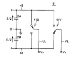
- FIG. 4 shows the single phase inverter comprised by the 2 level circuit. It is an equivalent circuit of the inverter 41 shown in FIG. FIG.
- FIG. 4 is a diagram illustrating a line voltage of an inverter 41.
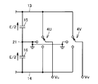
- FIG. 3 is an equivalent circuit diagram of a U-phase arm 4U and a V-phase arm 4V of the inverter 4 shown in FIG. It is the figure which showed the line voltage of the single phase 3 level inverter shown in FIG. It is a figure which shows the result of having simulated the reactor current at the time of setting the filter reactor provided in the output side of a 2 level inverter to 5%, and switching the inverter with the frequency of 10 kHz. It is a figure which shows the result of having simulated the reactor current at the time of setting the filter reactor provided in the output side of a 2 level inverter to 10%, and switching the inverter with the frequency of 10 kHz.
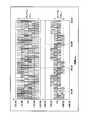
- FIG. 4 is a diagram showing switching patterns of IGBT elements Q1D to Q4D of FIG. 3 and voltages applied to a reactor 22.
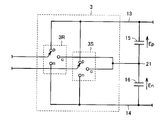
- FIG. 3 is an equivalent circuit diagram showing a configuration for two phases of converter 3 shown in FIG. 2.
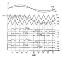
- FIG. 5 is a signal waveform diagram for explaining PWM control for one phase of converter 3 (three-level PWM converter) by converter control unit 53 shown in FIG. 4. It is the figure which showed the switching pattern of the four IGBT elements contained in each phase arm of a converter for every mode.
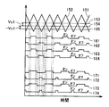
- FIG. 5 is a signal waveform diagram for explaining PWM control of the semiconductor switch 23 by the semiconductor switch control unit 54 shown in FIG. 4.
- 4 is a diagram showing switching patterns of IGBT elements Q1D to Q4D included in a semiconductor switch 23.
- FIG. It is a figure which shows the circuit of each mode shown in FIG. 29, and its electric current route.
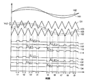
- It is a signal waveform diagram for demonstrating the balance control in case Ep ⁇ En by the semiconductor switch 23.
- FIG. It is a signal waveform diagram for demonstrating the balance control in case Ep> En by the semiconductor switch 23.
- FIG. It is a figure which shows the form which applied the power converter device of this invention to the three-phase four-wire system.
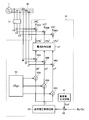
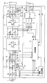
- FIG. 1 is a schematic block diagram showing a main circuit configuration of an uninterruptible power supply 100 according to an embodiment of the present invention.
- uninterruptible power supply 100 includes an input filter 2, a converter 3, an inverter 4, an output filter 5, a DC voltage converter (shown as “DC / DC” in the figure) 7, Control device 10, DC positive bus 13, DC negative bus 14, capacitors 15, 16, DC neutral point bus 17, voltage sensors 31, 34, 35, 36, current sensors 32, 37, power failure
- a detection circuit 33, an R-phase line RL, an S-phase line SL, and a T-phase line TL are provided.
- the input filter 2 prevents harmonics from flowing into the commercial AC power source 1.
- the commercial AC power source 1 is a three-phase AC power source.
- the input filter 2 is a three-phase LC filter circuit composed of a capacitor 11 (capacitors 11R, 11S, 11T) and a reactor 12 (reactors 12R, 12S, 12T).
- Converter 3 converts three-phase AC power supplied from commercial AC power supply 1 through input filter 2 to DC power, and supplies the DC power to inverter 4 via DC positive bus 13 and DC negative bus 14. To do.
- Inverter 4 converts the DC power from converter 3 into three-phase AC power. As will be described later, converter 3 and inverter 4 are constituted by a three-level circuit. Converter 3 and inverter 4 are connected via DC positive bus 13, DC negative bus 14, and DC neutral point bus 17.
- Capacitors 15 and 16 are connected in series between the DC positive bus 13 and the DC negative bus 14 to smooth the voltage between the DC positive bus 13 and the DC negative bus 14.
- a DC neutral point bus 17 is connected to a neutral point 21 which is a connection point of the capacitors 15 and 16.
- the output filter 5 removes harmonics generated by the operation of the inverter 4.
- the output filter 5 is a three-phase LC filter circuit constituted by a reactor 18 (reactors 18U, 18V, 18W) and a capacitor 19 (capacitors 19U, 19V, 19W).
- DC voltage converter 7 converts the voltage of storage battery 8 into a DC voltage between DC positive bus 13 and DC negative bus 14.
- the DC voltage converter 7 may be configured to mutually convert the DC voltage between the DC positive bus 13 and the DC negative bus 14 and the voltage of the storage battery 8.
- the DC voltage converter 7 only needs to be connected to a chargeable / dischargeable power storage device.
- an electric double layer capacitor may be connected to the DC voltage converter 7.
- the storage battery 8 is installed outside the uninterruptible power supply 100, but the storage battery 8 may be built in the uninterruptible power supply 100.
- the voltage sensor 31 detects the voltage VR of the R-phase line, the voltage VS of the S-phase line, and the voltage VT of the T-phase line, and outputs a three-phase voltage signal indicating the voltages VR, VS, and VT to the control device 10 and the power failure detection circuit 33. Output to.
- the current sensor 32 detects the current IR of the R-phase line, the current IS of the S-phase line, and the current IT of the T-phase line, and outputs a three-phase current signal indicating the voltages IR, IS, IT to the control device 10.
- the power failure detection circuit 33 detects a power failure of the commercial AC power supply 1 based on the three-phase voltage signal from the voltage sensor 31.
- the power failure detection circuit 33 outputs a power failure signal indicating a power failure of the commercial AC power supply 1 to the control device 10.
- the voltage between the DC positive bus 13 and the DC negative bus 14 is divided by the neutral point 21 into the voltages Ep and En.
- the voltage sensor 34 detects the voltage Ep across the capacitor 15 and outputs a signal indicating the voltage Ep to the control device 10.
- the voltage sensor 35 detects the voltage En across the capacitor 16 and outputs a signal indicating the voltage En to the control device 10.
- the voltage sensor 36 detects the voltage VB between the positive and negative electrodes of the storage battery 8 and outputs a signal indicating the voltage VB to the control device 10.
- Current sensor 37 detects current IB output from storage battery 8 and outputs a signal indicating current IB to control device 10.
- Control device 10 controls operations of converter 3, inverter 4, and DC voltage converter 7.
- converter 3, inverter 4, and DC voltage converter 7 are constituted by semiconductor switches including semiconductor switching elements.
- an IGBT Insulated Gate Bipolar Transistor
- PWM Pulse Width Modulation
- the control device 10 includes a three-phase voltage signal from the voltage sensor 31, a three-phase current signal from the current sensor 32, a signal indicating the voltage Ep detected by the voltage sensor 34, a signal indicating the voltage En detected by the voltage sensor 35, and a power failure detection.
- PWM control is executed in response to a power failure signal from the circuit 33, a signal indicating the voltage VB detected by the voltage sensor 36, a signal indicating the current IB detected by the current sensor 37, and the like.
- the converter 3 converts AC power from the commercial AC power source 1 into DC power
- the inverter 4 converts the DC power into AC power to the load 6. Supply.
- control device 10 stops converter 3 based on the power failure signal from power failure detection circuit 33. Further, the control device 10 operates the DC voltage converter 7 so that DC power is supplied from the storage battery 8 to the inverter 4, and continues supply of AC power by the inverter 4. In this case, the DC voltage converter 7 converts the voltage of the storage battery 8 into a suitable voltage as the input voltage of the inverter 4. Thereby, AC power can be stably supplied to the AC load.
- FIG. 2 is a circuit diagram illustrating in detail the configuration of the converter 3 and the inverter 4 shown in FIG.
- converter 3 includes an R-phase arm 3R, an S-phase arm 3S, and a T-phase arm 3T.
- Inverter 4 includes a U-phase arm 4U, a V-phase arm 4V, and a W-phase arm 4W.
- Each phase arm (3R, 3S, 3T) of converter 3 and each phase arm (4U, 4V, 4W) of inverter 4 are each configured as a three-level circuit, and include four IGBT elements and six diodes.
- R-phase arm 3R includes IGBT elements Q1R to Q4R and diodes D1R to D6R.
- S-phase arm 3S includes IGBT elements Q1S to Q4S and diodes D1S to D6S.
- T-phase arm 3T includes IGBT elements Q1T to Q4T and diodes D1T to D6T.
- U-phase arm 4U includes IGBT elements Q1U to Q4U and diodes D1U to D6U.
- V-phase arm 4V includes IGBT elements Q1V to Q4V and diodes D1V to D6V.
- W-phase arm 4W includes IGBT elements Q1W to Q4W and diodes D1W to D6W.
- IGBT elements Q1x-Q4x are connected in series between DC positive bus 13 and DC negative bus 14.
- Diodes D1x to D4x are connected in antiparallel to IGBT elements Q1x to Q4x, respectively.
- Diode D5x is connected to the connection point of IGBT elements Q1x and Q2x and neutral point 21.
- Diode D6x is connected to the connection point of IGBT elements Q3x and Q4x and neutral point 21.
- the cathode of the diode D5x is connected to the connection point between the IGBT elements Q1x and Q2x, and the anode of the diode D5x is connected to the neutral point 21.
- the anode of diode D6x is connected to the connection point of IGBT elements Q3x and Q4x, and the cathode of diode D6x is connected to neutral point 21.
- the diodes D1x to D4x function as freewheeling diodes, and the diodes D5x and D6x function as clamp diodes.
- connection point of IGBT elements Q2x, Q3x corresponds to the AC input terminal
- connection point of diodes D5x, D6x corresponds to the DC output terminal
- connection point of diodes D5x and D6x corresponds to the DC input terminal
- connection point of IGBT elements Q2x and Q3x corresponds to the AC output terminal
- each phase arm (3R, 3S, 3T) of converter 3 is connected to a corresponding line (R phase line RL, S phase line SL, T phase line TL), and each phase arm (4U, 4V, 4S) AC output terminals are connected to corresponding lines (U-phase line UL, V-phase line VL, W-phase line WL).
- the DC output terminal of each phase arm of converter 3 and the DC input terminal of each phase arm of inverter 4 are connected to neutral point 21.
- FIG. 3 is a diagram for explaining the configuration of the DC voltage converter 7 shown in FIG. 1 in detail.
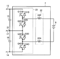
- DC voltage converter 7 includes a reactor 22 and a semiconductor switch 23.
- Semiconductor switch 23 includes IGBT elements Q1D to Q4D connected in series between DC positive bus 13 and DC negative bus 14, and diodes D1D to D4D connected in reverse parallel to IGBT elements Q1D to Q4D, respectively.
- one end of the reactor 22P is connected to the connection point of the IGBT elements Q1D and Q2D, and one end of the reactor 22N is connected to the connection point of the IGBT elements Q3D and Q4D.
- the other end of reactor 22P is connected to the positive electrode of storage battery 8
- the other end of reactor 22N is connected to the negative electrode of storage battery 8.
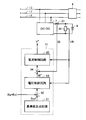
- FIG. 4 is a block diagram for explaining the control units of the converter 3 and the DC voltage converter 7 included in the control device 10.
- control device 10 includes an adder 51, a subtractor 52, a converter control unit 53, and a semiconductor switch control unit 54.
- the adder 51 adds the voltage value Ep indicating the voltage of the capacitor 15 detected by the voltage sensor 34 and the voltage value En of the capacitor 16 detected by the voltage sensor 35, and adds the DC positive bus 13 and the DC negative bus 14.
- the voltage value between (Ep + En) is output.
- the subtractor 52 subtracts the voltage value En from the voltage value Ep and outputs a voltage difference (Ep ⁇ En) value.
- Converter control unit 53 includes a voltage command generation circuit 61, a neutral point potential control circuit 62, adders 63A to 63C, a stop circuit 64, and a PWM circuit 65.
- the voltage command generation circuit 61 receives the voltages VR, VS, VT detected by the voltage sensor 31, the currents IR, IS, IT detected by the current sensor 32, and the voltage value (Ep + En) calculated by the adder 51, and R Voltage command values VR 0 * , VS 0 * , and VT 0 * respectively corresponding to the phase, the S phase, and the T phase are generated.
- the neutral point potential control circuit 62 receives a value indicating the voltage difference (Ep ⁇ En) from the subtractor 52 and generates a voltage command value V 1 * . For example, the neutral point potential control circuit 62 generates the voltage command value V 1 * by performing a proportional operation or a proportional integration operation on the voltage difference (Ep ⁇ En).
- the adder 63A the voltage command value VR 0 *, by adding V 1 * and generates a voltage command value VR *.
- the adder 63B is the voltage command value VS 0 *, by adding V 1 * and generates a voltage command value VS *.
- the adder 63C is the voltage command value VT 0 *, by adding V 1 * and generates a voltage command value VT *.
- Stop circuit 64 includes switches 64A to 64C.
- the signal from the power failure detection circuit 33 indicates that the commercial AC power supply 1 is normal (for example, when the logical value of the signal is “1”)
- the voltage command values VR * , VS * , and VT * are supplied to the PWM circuit 65.
- Switches 64A to 64C are set so as to be transmitted.
- the switches 64A to 64C are all grounded. As a result, the input of the voltage command value to the PWM circuit 65 is stopped, and simultaneously, an off signal is given to all the IGBT elements of the converter 3 and the converter 3 is stopped.
- the PWM circuit 65 is configured to make the voltages VR, VS, and VT detected by the voltage sensor 31 equal to the voltage command values VR * , VS * , and VT * based on the voltage command values VR * , VS * , and VT * , respectively. Output a signal.
- This signal is a signal for driving four IGBT elements included in each phase arm of converter 3.
- the semiconductor switch control unit 54 includes a voltage command generation circuit 71, a neutral point potential control circuit 72, an adder 73A, a subtractor 73B, a stop circuit 74, and a PWM circuit 75.
- the voltage command generation circuit 71 receives the voltage VB detected by the voltage sensor 36, the current IB detected by the current sensor 37, and the voltage value (Ep + En) calculated by the adder 51, and sets the voltage values Ep and En to predetermined voltages. A voltage command value V * for controlling the current is generated.
- the neutral point potential control circuit 72 receives a value indicating the voltage difference (Ep ⁇ En) from the subtractor 52 and generates a voltage command value VB 1 * .
- the neutral point potential control circuit 72 generates the voltage command value VB 1 * by performing a proportional operation or a proportional integration operation on the voltage difference (Ep ⁇ En). For example, when Ep ⁇ En> 0, the neutral point potential control circuit 72 sets the voltage command value VB 1 * to a negative value. On the other hand, when Ep ⁇ En ⁇ 0, neutral point potential control circuit 72 sets voltage command value VB 1 * to a positive value.
- the adder 73A is * the voltage command value V, by adding VB 1 * to generate a voltage command value VA *.
- the subtractor 73B subtracts the voltage command value VB 1 * from the voltage command value V * to generate a voltage command value VB * .
- the voltage command values VA * and VB * are command values for controlling the voltages of the upper and lower arms of the semiconductor switch 23, respectively, and commands for the voltages Ep and En for setting the difference between the voltages Ep and En to 0. Value.
- the neutral point potential control circuit 72, the adder 73A, and the subtractor 73B are arranged such that the voltage Ep, the voltage Ep, so that the voltage difference (Ep-En) becomes 0 based on the voltage difference (Ep-En) and the voltage command value V * .
- a command value generation circuit for generating voltage command values VA * and VB * for controlling En is configured.
- Stop circuit 74 includes switches 74A and 74B.
- the signal from the power failure detection circuit 33 indicates that the commercial AC power supply 1 is normal, both the switches 74A and 74B are grounded.
- the input of the voltage command value to the PWM circuit 75 is stopped, and at the same time, an off signal is given to all IGBT elements of the DC voltage converter 7, and the DC voltage converter 7 is stopped.
- the switches 74A and 74B transmit the voltage command values VA * and VB * to the PWM circuit 75, and the IGBT element of the DC voltage converter 7 Is set to be given an on / off command.
- the PWM circuit 75 outputs signals for driving the four IGBT elements included in the semiconductor switch 23 based on the voltage command values VA * and VB * .
- FIG. 5 is a functional block diagram of the voltage command generation circuit 61 shown in FIG. Referring to FIG. 5, voltage command generation circuit 61 includes reference value generation circuit 81, subtracters 82, 86A to 86C, DC voltage control circuit 83, sine wave generation circuit 84, and multipliers 85A to 85C. Current control circuit 87.
- the reference value generation circuit 81 generates a reference value Eref that is a reference value of the voltage value (Ep + En).
- the subtractor 82 calculates the difference between the reference value Eref and the voltage value (Ep + En) generated by the adder 51.
- DC voltage control circuit 83 calculates current command value I * for controlling the current flowing to the input side of converter 3 such that the difference between reference value Eref and voltage value (Ep + En) is zero.
- the DC voltage control circuit 83 calculates the current command value I * by, for example, performing a proportional operation or a proportional integration operation on the error between the reference value and the detected voltage value.
- the sine wave generation circuit 84 has a sine wave signal in phase with the R phase voltage of the commercial AC power supply 1, a sine wave signal in phase with the S phase voltage of the commercial AC power supply 1, and a T phase voltage of the commercial AC power supply 1.
- a sine wave signal is output.
- the three sine wave signals are respectively input to the multipliers 85A to 85C and multiplied by the current command value I * .
- current command values IR * , IS * , and IT * having the same phase as the phase voltage of the commercial AC power supply 1 are generated.
- Subtractor 86A calculates the difference between current command value IR * and R-phase current IR detected by current sensor 32.
- the subtractor 86B calculates a difference between the current command value IS * and the S-phase current IS detected by the current sensor 32.
- the subtractor 86C calculates the difference between the current command value IT * and the T-phase current IT detected by the current sensor 32.
- the current control circuit 87 has a difference between the current command value IR * and the R-phase current IR, a difference between the current command value IS * and the S-phase current IS, and a difference between the current command value IT * and the T-phase current IT. Also, voltage command values VRa * , VSa * , and VTa * are generated as voltages to be applied to the reactor 32 so as to be zero.
- the current control circuit 87 generates a voltage command value by, for example, amplifying the difference between the current command value and the current value detected by the current sensor according to proportional control or proportional integration control.
- Adder 88A adds voltage command value VRa * and R-phase voltage VR detected by voltage sensor 31 to generate voltage command value VR 0 * .
- Adder 88B adds voltage command value VSa * and S-phase voltage VS detected by voltage sensor 31 to generate voltage command value VS 0 * .
- Adder 88C adds voltage command value VTa * and T-phase voltage VT detected by voltage sensor 31 to generate voltage command value VT 0 * .
- the converter 3 Since the converter 3 is controlled by the converter control unit 53 having the above-described configuration, the currents IR, IS, and IT become in-phase and sinusoidal currents with the commercial AC power supply 1, so that the power factor can be set to approximately 1. it can.
- FIG. 6 is a functional block diagram of voltage command generation circuit 71 shown in FIG.
- voltage command generation circuit 71 includes a reference value generation circuit 91, a subtracter 92, a voltage control circuit 93, an adder 94, and a current control circuit 95.
- the reference value generation circuit 91 generates a reference value Eref that is a reference value of the voltage value (Ep + En).
- the subtractor 92 calculates a difference between the reference value Eref and the voltage value (Ep + En) generated by the adder 51.
- the voltage control circuit 93 calculates a current command value IB * corresponding to the difference between the reference value Eref and the voltage value (Ep + En) based on the voltage VB of the storage battery 8 detected by the voltage sensor 36.
- the voltage control circuit 93 calculates the current command value IB * by, for example, performing a proportional operation or a proportional integration operation on the error between the reference value and the detected voltage value.
- the adder 94 subtracts the current command value IB * generated by the voltage control circuit 93 and the current value IB of the storage battery 8 detected by the current sensor 37.
- the current control circuit 95 generates a voltage command value V * based on the difference between the current command value IB * and the current value IB.
- the converter 3 and the inverter 4 are configured by a three-level circuit.
- the inverter is generally constituted by a two-level circuit for the purpose of reducing the number of semiconductor switching elements. By configuring the inverter with a three-level circuit, higher harmonics can be suppressed than in a conventional power converter.
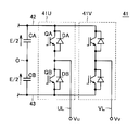
- FIG. 7 is a diagram showing a single-phase inverter configured by a two-level circuit.
- inverter 41 includes a U-phase arm 41U and a V-phase arm 41V.
- U-phase arm 41U and V-phase arm 41V are connected in parallel between DC positive bus 42 and DC negative bus 43, and have the same configuration.
- U-phase arm 41U includes IGBT elements QA and QB connected in series between DC positive bus 42 and DC negative bus 43, and diodes DA and DB connected in antiparallel to IGBT elements QA and QB, respectively.
- a U-phase line UL is connected to a connection point between IGBT elements QA and QB.
- V-phase arm 41V has a configuration in which U-phase line UL is replaced with V-phase line VL in the configuration of U-phase arm 41U.
- Capacitors CA and CB are connected in series between the DC positive bus 42 and the DC negative bus 43.
- a neutral point O is a connection point between the capacitors CA and CB.
- the voltage across capacitor CA and the voltage across capacitor CB are both E / 2 (E is a predetermined value).
- FIG. 8 is an equivalent circuit of the inverter 41 shown in FIG.
- U-phase arm 41 ⁇ / b> U is equivalent to a switch that switches the connection destination of U-phase line UL between DC positive bus 42 and DC negative bus 43.
- the neutral point O is grounded, the voltage Vu of the U-phase line UL is switched between E / 2 and ⁇ E / 2 when the switch is operated.
- the voltage Vv of the V-phase line VL changes in the same manner as the voltage Vu.
- the two-level circuit converts the DC voltage E into an AC voltage having two values (E / 2, ⁇ E / 2).
- FIG. 9 is a diagram showing the line voltage of the inverter 41.
- the line voltage difference between voltage Vu and voltage Vv
- the minimum change width of the line voltage is equal to the voltage E.
- FIG. 10 is an equivalent circuit diagram of U-phase arm 4U and V-phase arm 4V of inverter 4 shown in FIG.
- U-phase arm 4 ⁇ / b> U is equivalent to a switch that switches the connection destination of U-phase line UL among DC positive bus 13, neutral point 21, and DC negative bus 14.
- the voltage Vu of the U-phase line UL is switched between E / 2, 0, and ⁇ E / 2.
- the voltage Vv of the V-phase line VL changes similarly to the voltage Vu.
- the three-level circuit is a circuit capable of mutually converting a DC voltage and an AC voltage having three values.
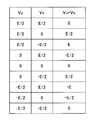
- FIG. 11 is a diagram showing the line voltage of the single-phase three-level inverter shown in FIG. Referring to FIG. 11, the line voltage (difference between voltage Vu and voltage Vv) switches between E, E / 2, 0, -E / 2, and -E. In an inverter composed of a three-level circuit (three-level inverter), the minimum change width of the line voltage is equal to E / 2.
- the change width of the line voltage is smaller in the 3-level inverter than in the 2-level inverter.
- the waveform of the output voltage of the inverter changes more finely, so that the waveform can be made closer to a sine wave.
- the harmonics generated by the operation of the inverter can be reduced. Therefore, the three-level inverter can reduce higher harmonics than the two-level inverter.
- FIG. 12 is a diagram showing a simulation result of the reactor current when the filter reactor provided on the output side of the two-level inverter is set to 5% and the inverter is switched at a frequency of 10 kHz.
- FIG. 13 is a diagram illustrating a result of simulating the reactor current when the filter reactor provided on the output side of the two-level inverter is set to 10% and the inverter is switched at a frequency of 10 kHz. From the simulations of FIGS. 12 and 13, comparing the total harmonic distortion (Total Harmonic Distortion; THD), when the reactor inductance is 5%, the THD is 6.4%, whereas the reactor inductance is By increasing to 10%, the THD was reduced to 3.2%.
- THD Total Harmonic Distortion
- THD represents the ratio between the effective value sum of the harmonic components and the effective value of the fundamental wave.
- Small THD means that the harmonic component is small.
- 12 and 13 show that the THD is reduced by increasing the reactor inductance. However, if the reactor inductance is increased in order to reduce the harmonic component, it is necessary to increase the number of turns of the coil, which causes a problem that the volume and weight of the reactor increase.
- FIG. 14 is a diagram showing a result of simulating the reactor current when the filter reactor provided on the output side of the three-level inverter is set to 5% and the inverter is switched at a frequency of 10 kHz.
- FIGS. 14 and 12 it can be seen that if the inductance of the filter reactor is the same, the three-level inverter can suppress higher harmonic components than the two-level inverter.
- the THD was 3.2%.
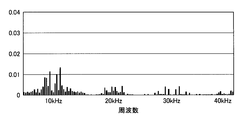
- FIG. 15 is a diagram showing a frequency spectrum of the harmonic current (FIG. 12) generated by the two-level inverter.
- FIG. 16 is a diagram showing a frequency spectrum of the harmonic current (FIG. 14) generated by the three-level inverter.
- the 3-level inverter can suppress higher harmonics than the 2-level inverter regardless of the frequency. Note that the frequency spectra of FIGS. 15 and 16 are obtained by simulation. In the simulation, the DC voltage input to the inverter is 500 V, the load is a three-phase resistance load of 10 kW, and the output voltage (line voltage) is 208 Vrms.
- the harmonics generated by the inverter can be reduced.
- the reactor which has small inductance can be used for a filter, the volume and weight of a reactor can be made small. Therefore, according to the present embodiment, the power converter can be reduced in size and weight.
- the following effects can be obtained by configuring the inverter with a three-level circuit.
- a storage battery having a large capacity is connected as a DC power source to the input side DC capacitor of the inverter.
- the inverter 4 is composed of a two-level inverter, the variation range of the output voltage is increased, so that the ground potential fluctuation is also increased.
- the change width of the output voltage can be reduced as compared with the case of the two-level inverter. As a result, ground potential fluctuation can be reduced, so that the amount of noise generation can be reduced.
- FIG. 17 is a diagram showing simulation results of ground potential fluctuation of the two-level inverter and ground potential fluctuation of the three-level inverter.
- the DC voltage input to the inverter was set to 360V.
- the ground potential fluctuation in the two-level inverter is 1 [p. u]
- the ground potential fluctuation in the three-level inverter is 0.5 [p. u].
- the three-level inverter can reduce the ground potential fluctuation.
- the loss of the inverter 4 can be reduced.
- the loss of the inverter 4 is a conduction loss (loss when the IGBT element and the diode are energized) and a switching loss of the IGBT element.
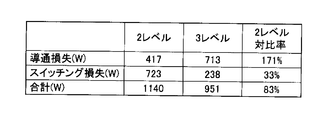
- FIG. 18 is a diagram showing simulation results of losses of the two-level inverter and the three-level inverter.
- FIG. 19 is a diagram for explaining the breakdown of losses of the two-level inverter and the three-level inverter.
- the DC input voltage is 600 V
- the switching frequency is 10 kHz
- the AC output voltage (line voltage) is 380 Vrms
- the load is 275 kW.
- the IGBT element included in the two-level inverter was a 1200V-600A product
- the IGBT element included in the three-level inverter was a 600V-600A product.
- the total loss of the three-level inverter is 83% of the total loss of the two-level inverter. This is because the switching loss is reduced. As shown in FIG. 18, the switching loss of the 3-level inverter is smaller than that of the 2-level inverter (33%). This is because the voltage applied to one semiconductor switching element can be made smaller in the three-level inverter than in the two-level inverter.
- the switching loss accounts for a large proportion (63%) of the total loss.
- a three-level inverter can greatly reduce this switching loss. Therefore, although the conduction loss increases in the three-level inverter as compared with the two-level inverter, the overall loss can be made smaller than that in the two-level inverter. By reducing the loss of the inverter, the operating efficiency of the power converter can be increased.
- the converter 3 is also constituted by a three-level circuit, so that the same effect as that of the inverter 4 can be obtained by the converter 3.
- the reactor included in the input filter can be reduced in size.
- the power converter can be further reduced in size and weight.
- the amount of noise generated by the converter 3 can also be reduced.
- the loss of converter 3 can be reduced, the operating efficiency of the power converter can be increased.
- the converter 3 and the inverter 4 can share components, so that the cost of the power converter can be reduced.
- the DC voltage converter 7 conventionally has a configuration in which two IGBT elements QC and QD are connected in series as shown by the semiconductor switch 44 in FIG.
- the ripple component of the current flowing through the reactor 22 is reduced by configuring a semiconductor switch by connecting four IGBT elements in series.
- a voltage of (E-VB) is applied to the reactor 45, and when the IGBT element QC is off and the IGBT element QD is on A voltage of ( ⁇ VB) is applied to the reactor 45. Therefore, the reactor voltage difference due to switching is E.
- E-VB a voltage of (E-VB)
- FIG. 21 shows the switching pattern of the IGBT elements Q1D to Q4D and the voltage applied to the reactor 22. From FIG. 21, it can be seen that the voltage that can be applied to the reactor 22 by the DC voltage converter 7 also has three levels. With the configuration of FIG. 3, the reactor voltage difference due to switching can be set to E / 2, and the ripple component of the current flowing through the reactor 22 can be reduced. Thereby, since the inductance of the reactor 22 can be reduced and the reactor 22 can be reduced in size, the power converter can be further reduced in size and weight.
- the inverter is configured by a three-level circuit, the positive and negative terminals on the DC side of the inverter It is necessary to connect a plurality of capacitors in series between them. Further, it is necessary to connect the DC neutral point bus 17 from the inverter 4 to the connection point (neutral point 21) of the capacitors 15 and 16.
- FIG. 22 is an equivalent circuit showing the configuration of two phases of the converter 3 shown in FIG. Referring to FIG. 22, in the equivalent circuit, each of R-phase arm 3R and S-phase arm 3S is shown as a switch. In this equivalent circuit, for example, the AC output in the inverter operation is one of three potential states (p, c, n).
- FIG. 23 is a signal waveform diagram for explaining PWM control for one phase of converter 3 (three-level PWM converter) by converter control unit 53 shown in FIG.
- the symbols of the four IGBT elements included in each phase arm are represented as Q1 to Q4.
- the voltage command signal 103 is a voltage command signal that has not been corrected by the neutral point potential control circuit 62.
- the PWM circuit 65 compares the voltage command signal 103 with the reference signals 101 and 102 to determine the switching patterns of the four IGBT elements included in the R phase (the S phase and the T phase are the same). Is done. In this case, the switching patterns of the IGBT elements Q1 to Q4 of the phase arm are the switching patterns 111 to 114, and the output voltage of the converter 3 is the phase voltage 106.
- the voltage command signal 104 is a voltage command signal corrected by the neutral point potential control circuit 62 when Ep ⁇ En, and is obtained by adding the adjustment signal Vc1 to the voltage command signal 103.
- the PWM circuit 65 compares the voltage command signal 104 with the reference signals 101 and 102 to determine the switching patterns of the four IGBT elements included in the R phase (the S phase and the T phase are the same). Is done. In this case, the switching patterns of the IGBT elements Q1 to Q4 of the phase arm are the switching patterns 121 to 124, and the output voltage of the converter 3 is the phase voltage 107.
- the voltage command signal 105 is a voltage command signal corrected by the neutral point potential control circuit 62 when Ep> En, and is obtained by adding the adjustment signal Vc2 to the voltage command signal 103.
- the PWM circuit 65 compares the voltage command signal 105 with the reference signals 101 and 102 to determine the switching patterns of the four IGBT elements included in the R phase (the S phase and the T phase are the same). Is done. In this case, the switching patterns of the IGBT elements Q1 to Q4 of the phase arm are the switching patterns 131 to 134, and the output voltage of the converter 3 is the phase voltage 108.
- the voltage command signal 103 corresponds to the voltage command values (VR 0 * , VS 0 * , VT 0 * ) from the voltage command generation circuit 61, and each of the adjustment signals Vc1, Vc2 is a neutral point potential control circuit. This corresponds to the voltage command value V 1 * from 62.
- the voltage command value V 1 * is positive when Ep ⁇ En, and is negative when Ep> En.
- FIG. 23 shows that the switching pattern of the phase-arm IGBT element is composed of three modes.
- FIG. 24 shows switching patterns of four IGBT elements included in the R phase (the same applies to the S phase and the T phase) for each mode.
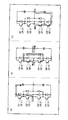
- FIG. 25 shows a circuit for one phase in each mode shown in FIG. 24 and its current route.
- FIG. 25 (a) shows mode 1. In mode 1, the positive-side smoothing capacitor 15 is charged. Mode 2 is shown in FIG. In mode 2, the storage states of the positive-side smoothing capacitor 15 and the negative-side smoothing capacitor 16 do not change much. Mode 3 is shown in FIG. In mode 3, the negative-side smoothing capacitor 16 is charged.
- FIG. 26 is a signal waveform diagram for explaining the balance control in the case of Ep ⁇ En by the converter 3.
- the neutral point potential control circuit 62 adds the adjustment signal Vc1 to the voltage command signal 103 in order to balance the voltages of the smoothing capacitors 15 and 16, and the voltage The command signal is adjusted to become the voltage command signal 104.
- the voltage command signal 104 and the reference signals 101 and 102 are compared in level to obtain the switching patterns 121 to 124 of the IGBT elements Q1 to Q4.
- the positive-side smoothing capacitor 15 is charged.
- the negative-side smoothing capacitor 16 is charged.
- the charging period of the positive smoothing capacitor 15 is longer than the charging period of the negative smoothing capacitor 16,
- FIG. 27 is a signal waveform diagram for explaining the balance control in the case of Ep> En by the converter 3.
- the neutral point potential control circuit 62 adds the adjustment signal Vc2 to the voltage command signal 103 in order to balance the voltages of the smoothing capacitors 15 and 16, and the voltage The command signal is adjusted to become the voltage command signal 105.
- the voltage command signal 105 and the reference signals 101 and 102 are compared in level to obtain the switching patterns 131 to 134 of the IGBT elements Q1 to Q4. During the periods t1, t2, t3, and t4 where the input phase voltage 141 and the phase current 142 are positive, the positive-side smoothing capacitor 15 is charged.
- the negative-side smoothing capacitor 16 is charged.
- the charging period of the positive smoothing capacitor 15 is shorter than the charging period of the negative smoothing capacitor 16,
- Vc1 represents the voltage of the adjustment signal Vc1.
- FIG. 28 is a signal waveform diagram for explaining PWM control of the semiconductor switch 23 by the semiconductor switch control unit 54 shown in FIG. Referring to FIG.
- the neutral point potential control circuit 72 changes the voltage command signal of the IGBT elements Q1D and Q3D to the voltage command signal 153 by adding the adjustment signal Vc1 to the voltage command signal 154. Further, the neutral point potential control circuit 72 changes the voltage command signals of the IGBT elements Q2D and Q4D to the corrected voltage command signal 155 by subtracting the adjustment signal Vc1 from the command signal 154.
- FIG. 29 shows switching patterns of IGBT elements Q1D to Q4D.
- FIG. 30 shows a circuit of each mode shown in FIG. 29 and its current route.
- Fig. 30 (a) shows mode 1. In mode 1, the positive-side smoothing capacitor 15 is charged. Mode 2 is shown in FIG. In mode 2, the storage states of the positive-side smoothing capacitor 15 and the negative-side smoothing capacitor 16 do not change much. Mode 3 is shown in FIG. In mode 3, the negative-side smoothing capacitor 16 is charged.
- the PWM circuit 75 compares the voltage command signal 154 with the reference signal 151 to obtain the switching patterns 161 and 163 of the IGBT elements Q1 and Q3. Further, the PWM circuit 75 compares the voltage command signal 154 and the reference signal 152 with each other to obtain the switching patterns 162 and 164 of the IGBT elements Q2 and Q4. As a result, as shown in FIG. 31, IGBT elements Q1D to Q4D are operated in mode 1 during period t1 in each period T of reference signal 151, and positive-side smoothing capacitor 15 is charged. Further, the IGBT elements Q1D to Q4D are operated in the mode 3 during the period t2 in each cycle T of the reference signal 152, and the negative-side smoothing capacitor 16 is charged.
- the switching patterns 171 and 173 of the IGBT elements Q1D and Q3D are obtained by comparing the level of the voltage command signal 153 and the reference signal 151. Further, by comparing the level of voltage command signal 155 with reference signal 152, switching patterns 172 and 174 of IGBT elements Q2D and Q4D are obtained. In this case, as shown in FIG. 31, during the period t1 'of each cycle T of the reference signal 151, the IGBT elements Q1D to Q4D are operated in mode 1 and the positive-side smoothing capacitor 15 is charged.
- the IGBT elements Q1D to Q4D are operated in mode 3 and the negative-side smoothing capacitor 16 is charged.
- the neutral point potential control circuit 72 adds the adjustment signal Vc1 to the voltage command signal 154, thereby changing the voltage command signals of the IGBT elements Q1D and Q3D to the voltage command signal 155. Further, the neutral point potential control circuit 72 changes the voltage command signal of the IGBT elements Q2D and Q4D to the corrected voltage command signal 153 by subtracting the adjustment signal Vc1 from the command signal 154.
- switching patterns 181 and 183 shown in FIG. 32 are obtained as switching patterns of the IGBT elements Q1D and Q3D. Further, in the PWM circuit 75, the voltage command signal 153 and the reference signal 152 are compared in level to obtain the switching patterns 182 and 184 shown in FIG. 32 as the switching patterns of the IGBT elements Q2D and Q4D.
- the duty ratio of mode 1 and mode 3 changes depending on the adjustment signal Vc1, but the duty ratio of the period in which mode 1 and mode 3 are added does not change.
- the same adjustment signal Vc1 is added to one of the two voltage command signals and subtracted to the other, the voltage of the smoothing capacitors 15 and 16 is not affected by the boosting operation of the DC voltage converter 7. Can control the balance.
- d14 ′ d
- the balance control can be executed by the DC voltage converter 7 (semiconductor switch 23) at the time of a power failure of the commercial AC power supply. Therefore, according to the present embodiment, the balance control of the DC capacitor (smoothing capacitor) can be executed without adding a special circuit.
- the DC voltage converter may perform an operation of converting a DC voltage output from the converter into a charging voltage of the storage battery during the operation of the converter.
- only one of the DC voltage converter and the converter is not limited to be supplied with DC power to the inverter, and both the DC voltage converter and the converter may supply DC power to the inverter.
- the circuits constituting the inverter, the converter, and the DC voltage converter mutually convert the DC voltage and the AC voltage or DC voltage having at least three voltage values. Any circuit (multi-level circuit) may be used. Therefore, a 5-level circuit that mutually converts a DC voltage and an AC voltage having at least five voltage values can be applied to an inverter or the like.
- an uninterruptible power supply that can be applied to a three-phase three-wire AC power supply and a load is shown, but the present invention is also applicable to a three-phase four-wire AC power supply and a load, In the case of three-phase four-wire, as shown in FIG. 33, the middle point of the capacitors 11 and 19 and the neutral point 21 may be connected. Further, the AC power source and the AC load are not limited to three-phase ones and may be single-phase ones. In this case, each of the converter and the inverter only needs to include two multilevel circuits.
- a filter using a multilevel circuit is reduced in size and weight, and ground potential fluctuation suppression is applied to a photovoltaic power generation system, a fuel cell
- the present invention can be applied to a power conversion device that outputs AC power from DC power, such as a power generation system or a secondary battery energy storage system.
Landscapes
- Engineering & Computer Science (AREA)
- Power Engineering (AREA)
- Business, Economics & Management (AREA)
- Emergency Management (AREA)
- Inverter Devices (AREA)
- Rectifiers (AREA)
- Dc-Dc Converters (AREA)
Abstract
Description
Vu'=Vu+Vc1
Vv'=Vv+Vc1
Vw'=Vw+Vc1
(2)補正前の線間電圧:
Vuv=Vu-Vv
Vvw=Vv-Vw
Vwu=Vw-Vu
(3)補正後の線間電圧:
Vuv’=Vu’-Vv’=Vu+Vc1-Vv-Vc1=Vu-Vv=Vuv
Vvw’=Vv’-Vw’=Vv+Vc1-Vw-Vc1=Vv-Vw=Vvw
Vwu’=Vw’-Vu’=Vw+Vc1-Vu-Vc1=Vw-Vu=Vwu
次に、半導体スイッチ23および半導体スイッチ制御部54による、平滑コンデンサの電位制御について説明する。図28は、図4に示す半導体スイッチ制御部54による、半導体スイッチ23のPWM制御を説明するための信号波形図である。図28を参照して、電圧指令信号154は中性点電位制御回路72により補正されていない状態の電圧指令信号である。
IGBT素子Q1D,Q3Dのデューティ比d13:
d13=t1/T
IGBT素子Q2D,Q4Dのデューティ比d24:
d24=t2/T
IGBT素子Q1~Q4のデューティ比d14:
d14=d13+d24=(t1+t2)/T
(2)電圧指令信号信号153及び155に対するデューティ比
IGBT素子Q1、Q3のデューティ比d13’:
d13’=t1’/T
IGBT素子Q2、Q4のデューティ比d24’:
d24’=t2’/T
IGBT素子Q1~Q4のデューティ比d14’:
d14’=d13’+d24’=(t1’+t2’)/T=(t1+t2)/T=d14
以上説明したように、本実施の形態では、コンバータ3および直流電圧変換器7に含まれる半導体スイッチ23が3レベル回路により構成されるので、商用交流電源の正常時にはコンバータ3によってバランス制御を実行することができ、商用交流電源の停電時には直流電圧変換器7(半導体スイッチ23)によってバランス制御を実行できる。したがって、本実施の形態によれば、直流コンデンサ(平滑コンデンサ)のバランス制御を特別な回路を追加することなく実行できる。
Claims (6)
- 直流正母線(13)および直流負母線(14)との間に直列に接続される第1および第2のコンデンサ(15,16)と、
直流電圧と少なくとも3つの電圧値の間で変化する交流電圧とを相互に変換可能に構成され、かつ前記直流正母線(13)と前記直流負母線(14)と前記第1および第2のコンデンサ(15,16)の中性点(21)とに接続された第1のマルチレベル回路(4U)を含み、直流電力を交流電力に変換して負荷(6)に供給する第1の変換器(4)と、
前記第1のマルチレベル回路(4U)と同じ構成を有し、かつ前記直流正母線(13)、前記直流負母線(14)および前記中性点(21)に第1のマルチレベル回路(4U)と並列に接続された第2のマルチレベル回路(3R)を含み、交流電源からの交流電力を直流電力に変換して前記第1の変換器(4)に供給する第2の変換器(3)と、
直流電力を前記第1の変換器(4)に供給する直流電力供給源(8)と、
リアクトル(18)およびコンデンサ(19)を含み、前記第1の変換器(4)により発生する高調波を除去するフィルタ(5)と、
前記第2のマルチレベル回路(3R)の動作を制御することにより前記中性点(21)の電位変動を抑制する制御装置(10)とを備える、電力変換装置。 - 直流正母線(13)および直流負母線(14)との間に直列に接続される第1および第2のコンデンサ(15,16)と、
直流電圧と少なくとも3つの電圧値の間で変化する交流電圧とを相互に変換可能に構成され、かつ前記直流正母線(13)と前記直流負母線(14)と前記第1および第2のコンデンサ(15,16)の中性点(21)とに接続された第1のマルチレベル回路(4U)を含み、直流電力を交流電力に変換して負荷(6)に供給する第1の変換器(4)と、
前記第1のマルチレベル回路(4U)と同じ構成を有し、かつ前記直流正母線(13)、前記直流負母線(14)および前記中性点(21)に第1のマルチレベル回路(4U)と並列に接続された第2のマルチレベル回路(3R)を含み、交流電源からの交流電力を直流電力に変換して前記第1の変換器(4)に供給する第2の変換器(3)と、
直流電圧と少なくとも3つの電圧値の間で変化する直流電圧とを相互に変換可能に構成され、かつ前記直流正母線(13)、前記直流負母線(14)および前記中性点(21)に前記第1および第2のマルチレベル回路に並列に接続された第3のマルチレベル回路(23)を含み、直流電力供給源(8)からの直流電力の電圧値を変換して、前記第1の変換器(4)に前記直流電力供給源(8)からの直流電力を供給する第3の変換器(7)と、
リアクトル(18)およびコンデンサ(19)を含み、前記第1の変換器(4)により発生する高調波を除去するフィルタ(5)と、
前記第3のマルチレベル回路(23)の動作を制御することにより前記中性点(21)の電位変動を抑制する制御装置(10)とを備える、電力変換装置。 - 直流正母線(13)および直流負母線(14)との間に直列に接続される第1および第2のコンデンサ(15,16)と、
直流電圧と少なくとも3つの電圧値の間で変化する交流電圧とを相互に変換可能に構成され、かつ前記直流正母線(13)と前記直流負母線(14)と前記第1および第2のコンデンサ(15,16)の中性点(21)とに接続された第1のマルチレベル回路(4U)を含み、直流電力を交流電力に変換して負荷(6)に供給する第1の変換器(4)と、
前記第1のマルチレベル回路(4U)と同じ構成を有し、かつ前記直流正母線(13)、前記直流負母線(14)および前記中性点(21)に第1のマルチレベル回路(4U)と並列に接続された第2のマルチレベル回路(3R)を含み、交流電源からの交流電力を直流電力に変換して前記第1の変換器(4)に供給する第2の変換器(3)と、
直流電圧と少なくとも3つの電圧値の間で変化する直流電圧とを相互に変換可能に構成され、かつ前記直流正母線(13)、前記直流負母線(14)および前記中性点(21)に前記第1および第2のマルチレベル回路に並列に接続された第3のマルチレベル回路(23)を含み、直流電力供給源(8)からの直流電力の電圧値を変換して、前記第1の変換器(4)に前記直流電力供給源(8)からの直流電力を供給する第3の変換器(7)と、
リアクトル(18)およびコンデンサ(19)を含み、前記第1の変換器(4)により発生する高調波を除去するフィルタ(5)と、
前記第2および第3のマルチレベル回路(3R,23)の動作を制御することにより前記中性点(21)の電位変動を抑制する制御装置(10)とを備える、電力変換装置。 - 前記制御装置(10)は、前記交流電源(1)による電力供給が正常である場合には、前記第2のマルチレベル回路(3R)を動作させ、かつ前記第3のマルチレベル回路(23)を停止させる一方、前記交流電源(1)による前記電力供給が異常である場合には、前記第2のマルチレベル回路(3R)を停止させ、かつ前記第3のマルチレベル回路(23)を動作させる、請求の範囲第3項に記載の電力変換装置。
- 前記制御装置(10)は、前記第1のコンデンサ(15)の両端の電圧(Ep)と前記第2のコンデンサ(16)の両端の電圧(En)との差に基づいて、前記第1のコンデンサ(15)の充電期間および前記第2のコンデンサ(16)の充電期間が変化するように、対応するマルチレベル回路を制御することにより、前記中性点(21)の前記電位変動を抑制する、請求の範囲第1項から第4項のいずれか1項に記載の電力変換装置。
- 前記第1のマルチレベル回路(4U)は、
前記直流正母線(13)と前記直流負母線(14)との間に直列に接続される第1から第4の半導体スイッチング素子(Q1U~Q4U)と、
前記第1から第4の半導体スイッチング素子(Q1U~Q4U)にそれぞれ逆並列接続される第1から第4の還流ダイオード(D1U~D4U)と、
前記中性点(21)と前記第1および第2の半導体スイッチング素子(Q1U,Q2U)の接続点との間に接続される第1のクランプダイオード(D5U)と、
前記中性点(21)と前記第3および第4の半導体スイッチング素子(Q3U,Q4U)の接続点との間に接続される第2のクランプダイオード(D6U)とを含む、請求の範囲第1項から第5項のいずれか1項に記載の電力変換装置。
Priority Applications (8)
| Application Number | Priority Date | Filing Date | Title |
|---|---|---|---|
| JP2010525537A JP5463289B2 (ja) | 2008-08-22 | 2008-08-22 | 電力変換装置 |
| CN200880130914.2A CN102132480B (zh) | 2008-08-22 | 2008-08-22 | 功率转换装置 |
| PCT/JP2008/064966 WO2010021052A1 (ja) | 2008-08-22 | 2008-08-22 | 電力変換装置 |
| US13/057,102 US8400792B2 (en) | 2008-08-22 | 2008-08-22 | Power conversion apparatus |
| KR1020117003901A KR101230743B1 (ko) | 2008-08-22 | 2008-08-22 | 전력 변환 장치 |
| MX2011001963A MX2011001963A (es) | 2008-08-22 | 2008-08-22 | Aparato de conversion de energia. |
| CA2734699A CA2734699C (en) | 2008-08-22 | 2008-08-22 | Power conversion apparatus |
| JP2013111881A JP5631445B2 (ja) | 2008-08-22 | 2013-05-28 | 電力変換装置 |
Applications Claiming Priority (1)
| Application Number | Priority Date | Filing Date | Title |
|---|---|---|---|
| PCT/JP2008/064966 WO2010021052A1 (ja) | 2008-08-22 | 2008-08-22 | 電力変換装置 |
Publications (1)
| Publication Number | Publication Date |
|---|---|
| WO2010021052A1 true WO2010021052A1 (ja) | 2010-02-25 |
Family
ID=41706948
Family Applications (1)
| Application Number | Title | Priority Date | Filing Date |
|---|---|---|---|
| PCT/JP2008/064966 Ceased WO2010021052A1 (ja) | 2008-08-22 | 2008-08-22 | 電力変換装置 |
Country Status (7)
| Country | Link |
|---|---|
| US (1) | US8400792B2 (ja) |
| JP (1) | JP5463289B2 (ja) |
| KR (1) | KR101230743B1 (ja) |
| CN (1) | CN102132480B (ja) |
| CA (1) | CA2734699C (ja) |
| MX (1) | MX2011001963A (ja) |
| WO (1) | WO2010021052A1 (ja) |
Cited By (13)
| Publication number | Priority date | Publication date | Assignee | Title |
|---|---|---|---|---|
| JP2013005649A (ja) * | 2011-06-20 | 2013-01-07 | Fuji Electric Co Ltd | 直流電源システム |
| WO2013099053A1 (ja) * | 2011-12-28 | 2013-07-04 | パナソニック株式会社 | マルチレベルインバータ装置 |
| WO2013157387A1 (ja) * | 2012-04-16 | 2013-10-24 | 東芝キヤリア株式会社 | 整流装置および整流システム |
| JP2013230027A (ja) * | 2012-04-26 | 2013-11-07 | Fuji Electric Co Ltd | 交流電源システム |
| JP2013247724A (ja) * | 2012-05-24 | 2013-12-09 | Hitachi Ltd | 無停電電源装置、無停電電源装置の制御方法 |
| JP2015033326A (ja) * | 2013-07-31 | 2015-02-16 | アーベーベー・テクノロジー・アーゲー | 電源システム、電源システムを動作させるための方法、およびコントローラ |
| JP2015042112A (ja) * | 2013-08-23 | 2015-03-02 | 東芝三菱電機産業システム株式会社 | 無停電電源システム |
| WO2015063898A1 (ja) * | 2013-10-30 | 2015-05-07 | 三菱電機株式会社 | 直流/直流変換装置および負荷駆動制御システム |
| JPWO2016157469A1 (ja) * | 2015-04-01 | 2017-11-09 | 東芝三菱電機産業システム株式会社 | 無停電電源装置およびそれを用いた無停電電源システム |
| JP2019058021A (ja) * | 2017-09-22 | 2019-04-11 | 富士電機株式会社 | 3レベルチョッパ及びその制御回路 |
| JP6571903B1 (ja) * | 2018-11-20 | 2019-09-04 | 東芝三菱電機産業システム株式会社 | 無停電電源装置 |
| WO2019207772A1 (ja) * | 2018-04-27 | 2019-10-31 | 東芝三菱電機産業システム株式会社 | 3レベル電力変換装置、3レベル電力変換装置の制御方法、及び記憶媒体 |
| WO2020026430A1 (ja) * | 2018-08-03 | 2020-02-06 | 東芝三菱電機産業システム株式会社 | 無停電電源装置 |
Families Citing this family (72)
| Publication number | Priority date | Publication date | Assignee | Title |
|---|---|---|---|---|
| JP5486604B2 (ja) | 2009-09-25 | 2014-05-07 | 東芝三菱電機産業システム株式会社 | 無停電電源装置 |
| KR101314886B1 (ko) | 2009-09-30 | 2013-10-04 | 도시바 미쓰비시덴키 산교시스템 가부시키가이샤 | 전력 변환 시스템 |
| CN102948061B (zh) * | 2010-06-23 | 2015-06-17 | 住友重机械工业株式会社 | 注射成形机及电源再生转换器 |
| JP5163734B2 (ja) * | 2010-12-17 | 2013-03-13 | 富士電機株式会社 | 3レベルインバータ装置 |
| US9136709B2 (en) * | 2011-10-26 | 2015-09-15 | General Electric Company | Methods and systems for selectively coupling a power conversion system to an electrical grid |
| CN103138595B (zh) * | 2011-11-22 | 2016-05-25 | 通用电气公司 | 中点箝位式变流器的控制系统及控制方法 |
| US9099934B2 (en) * | 2012-01-10 | 2015-08-04 | Yaskawa America, Inc. | Three phase active rectifier system |
| JP5822732B2 (ja) | 2012-01-11 | 2015-11-24 | 東芝三菱電機産業システム株式会社 | 3レベル電力変換装置 |
| JP5770929B2 (ja) * | 2012-03-30 | 2015-08-26 | 東芝三菱電機産業システム株式会社 | 電源装置 |
| US8861230B2 (en) | 2012-05-30 | 2014-10-14 | Astec International Limited | Control circuits for power converters |
| CN102751882A (zh) * | 2012-07-14 | 2012-10-24 | 张翔 | 三相中性点钳位式四象限运行的三电平电源变换装置 |
| JP2014090581A (ja) * | 2012-10-30 | 2014-05-15 | Toshiba Corp | 電力変換装置および電力変換方法 |
| US9362844B2 (en) * | 2013-06-14 | 2016-06-07 | Hamilton Sundstrand Corporation | Method of deriving switch current signals in a rectifier |
| DE102013108670A1 (de) * | 2013-08-09 | 2015-02-12 | Ge Energy Power Conversion Gmbh | Verfahren und Vorrichtung zum Betreiben eines Stromrichters |
| CN105723584B (zh) * | 2013-08-23 | 2018-06-05 | Abb瑞士股份有限公司 | 在配电系统中运行变换器的方法和装置以及配电系统 |
| US9450513B2 (en) * | 2013-09-27 | 2016-09-20 | Daihen Corporation | Control circuit and control method for inverter circuit, and control circuit and control method for power conversion circuit |
| EP2882088A1 (en) * | 2013-12-06 | 2015-06-10 | Siemens Aktiengesellschaft | 3-level inverter |
| US9941738B2 (en) | 2013-12-23 | 2018-04-10 | Schneider Electric It Corporation | Dynamic DC link voltage control |
| WO2015118122A1 (en) * | 2014-02-07 | 2015-08-13 | Abb Technology Ag | Uninterruptable power supply with balancing buck/boost converter |
| KR101399118B1 (ko) * | 2014-03-10 | 2014-05-27 | (주)티피에스 | 전력 변환 장치 |
| CN106663940B (zh) | 2014-06-27 | 2019-08-06 | 施耐德电气It公司 | 三级电力拓扑 |
| JP5931148B2 (ja) | 2014-09-10 | 2016-06-08 | ファナック株式会社 | 静電容量計算部を有するpwm整流器 |
| JP6342293B2 (ja) * | 2014-10-20 | 2018-06-13 | 株式会社東芝 | 中性点クランプ形電力変換装置およびその制御方法 |
| JP6264257B2 (ja) * | 2014-10-20 | 2018-01-24 | 株式会社明電舎 | 三相中性点クランプ式の電力変換装置 |
| WO2016100026A1 (en) * | 2014-12-17 | 2016-06-23 | Otis Elevator Company | Conveyance system having paralleled drives |
| JP6426462B2 (ja) * | 2014-12-24 | 2018-11-21 | 株式会社東芝 | 電力変換装置およびその制御方法 |
| JP6243575B2 (ja) * | 2015-04-01 | 2017-12-06 | 東芝三菱電機産業システム株式会社 | 無停電電源装置およびそれを用いた無停電電源システム |
| MX361850B (es) * | 2015-06-23 | 2018-12-18 | Nissan Motor | Inversor con capacidad de carga. |
| JP6348460B2 (ja) * | 2015-07-08 | 2018-06-27 | 東芝三菱電機産業システム株式会社 | 電力変換システム |
| US11205919B2 (en) | 2015-09-30 | 2021-12-21 | Toshiba Mitsubishi-Electric Industrial Systems Corporation | Uninterruptible power supply system |
| KR101627620B1 (ko) * | 2015-12-03 | 2016-06-07 | 성신전기공업(주) | 무정전 전원장치 |
| WO2017125067A1 (en) * | 2016-01-22 | 2017-07-27 | The University Of Hong Kong | Power supply supporting virtual inertia for grid control (micro-spring converter) |
| US9800133B2 (en) * | 2016-03-22 | 2017-10-24 | Infineon Technologies Ag | Active common mode cancellation |
| US10211672B2 (en) * | 2016-10-13 | 2019-02-19 | Schneider Electric It Corporation | DC-link bus balancer |
| CN108566071B (zh) | 2016-12-16 | 2021-04-20 | 台达电子企业管理(上海)有限公司 | 模块化电源系统 |
| CN110463028B (zh) | 2017-01-30 | 2023-04-28 | 开利公司 | 对采用和不采用交织并联无源前端整流器进行控制的方法 |
| WO2018140744A1 (en) | 2017-01-30 | 2018-08-02 | Carrier Corporation | Paralleled passive front-end rectifiers with and without interleaving |
| US10185141B2 (en) * | 2017-06-23 | 2019-01-22 | General Electric Company | Cascaded electrical device bus structure systems and methods |
| US11329573B2 (en) * | 2017-08-04 | 2022-05-10 | Panasonic Intellectual Property Management Co., Ltd. | Power converter and power conversion system |
| GB2566479B (en) * | 2017-09-14 | 2019-10-23 | Eltek As | DC-DC Converter |
| US11394295B2 (en) * | 2017-09-27 | 2022-07-19 | Toshiba Mitsubishi-Electric Industrial Systems Corporation | Power supply apparatus |
| WO2019088678A1 (en) * | 2017-11-02 | 2019-05-09 | Samsung Electronics Co., Ltd. | Air conditioner and rectifier |
| JP7034670B2 (ja) * | 2017-11-02 | 2022-03-14 | 三星電子株式会社 | 整流装置、電源装置、電動機装置及び空調装置 |
| JP7000804B2 (ja) * | 2017-11-13 | 2022-01-19 | Tdk株式会社 | 電源装置 |
| JP6909867B2 (ja) * | 2017-11-30 | 2021-07-28 | 株式会社東芝 | 電圧補償装置 |
| KR101836872B1 (ko) * | 2018-01-15 | 2018-03-09 | 주식회사 에코스 | 3-레벨 컨버터의 직류측 전류를 일정하게 만드는 pwm 제어방법 및 장치 |
| CN110120736B (zh) | 2018-02-05 | 2021-04-23 | 台达电子企业管理(上海)有限公司 | 水冷电源模块 |
| KR102143363B1 (ko) * | 2018-03-30 | 2020-08-11 | 성신전기공업(주) | 3 레벨 인터리브드 충방전기를 가지는 전기에너지 저장 시스템 |
| SG11202011091QA (en) * | 2018-05-10 | 2020-12-30 | Toshiba Kk | Dc transformation system |
| US10516365B1 (en) * | 2018-06-20 | 2019-12-24 | Schneider Electric Solar Inverters Usa, Inc. | DC voltage control in renewable energy based multilevel power converter |
| JP6522211B1 (ja) * | 2018-07-02 | 2019-05-29 | 三菱電機株式会社 | 電力変換装置 |
| CN110798088B (zh) * | 2018-08-01 | 2021-12-17 | 株式会社安川电机 | 电力转换装置和控制方法 |
| EP3883115A4 (en) * | 2018-11-14 | 2022-06-22 | Toshiba Mitsubishi-Electric Industrial Systems Corporation | CURRENT TRANSFORMING DEVICE |
| EP3675345A1 (en) * | 2018-12-31 | 2020-07-01 | Solaredge Technologies Ltd. | Balanced capacitor power converter |
| JP6928013B2 (ja) * | 2019-01-09 | 2021-09-01 | ファナック株式会社 | 電源装置 |
| US11855548B2 (en) * | 2019-06-04 | 2023-12-26 | Toshiba Mitsubishi-Electric Industrial Systems Corporation | Power conversion device and power conversion control device |
| CN114270688A (zh) * | 2019-08-30 | 2022-04-01 | 三菱电机株式会社 | 电力变换装置以及空气调节机 |
| JP6771693B1 (ja) | 2019-08-30 | 2020-10-21 | 三菱電機株式会社 | 電力変換装置 |
| JP7214040B2 (ja) * | 2020-03-27 | 2023-01-27 | 三菱電機株式会社 | 3レベル電力変換装置及び直流電源部の中間電位の制御方法 |
| WO2021217622A1 (zh) * | 2020-04-30 | 2021-11-04 | 华为数字能源技术有限公司 | 一种电力电子变压器及供电系统 |
| CN113938045B (zh) * | 2020-06-28 | 2025-08-19 | 株洲中车时代电气股份有限公司 | 一种四流制辅助变流器、供电方法及系统 |
| CN114069819A (zh) * | 2020-08-07 | 2022-02-18 | 台达电子工业股份有限公司 | 具有三阶层切换电路的转换装置及三阶层切换电路的操作方法 |
| WO2022051892A1 (zh) * | 2020-09-08 | 2022-03-17 | 华为数字能源技术有限公司 | 一种三电平逆变器、控制方法及系统 |
| JP7130024B2 (ja) * | 2020-11-12 | 2022-09-02 | 三菱電機株式会社 | 電力変換装置 |
| KR102613335B1 (ko) * | 2021-04-20 | 2023-12-14 | 현대엘리베이터주식회사 | 엘리베이터용 전력변환장치 |
| KR102297964B1 (ko) * | 2021-04-30 | 2021-09-02 | 이길호 | 3상 4선식 구조를 갖는 무정전 전원 장치의 제어 방법 및 그 장치 |
| EP4087113B1 (en) | 2021-05-06 | 2025-07-02 | ABB Schweiz AG | Double-boost dc/dc converter |
| JP7620501B2 (ja) * | 2021-05-28 | 2025-01-23 | Tdk株式会社 | 補助電力供給装置、電源装置、及び医療システム |
| CN113852174B (zh) * | 2021-08-24 | 2024-03-01 | 北京精密机电控制设备研究所 | 一种用于野外环境的独立移动式油田储能电源系统 |
| EP4282066B1 (en) * | 2021-11-22 | 2026-03-04 | Huawei Technologies Co., Ltd. | Controller for controlling a balancer circuit |
| US12282045B2 (en) | 2022-12-02 | 2025-04-22 | Infineon Technologies Ag | Common mode evaluation in a differential galvanic isolation signal transmission circuit |
| US12512745B2 (en) * | 2023-09-14 | 2025-12-30 | Kabushiki Kaisha Toyota Jidoshokki | Power conversion device |
Citations (5)
| Publication number | Priority date | Publication date | Assignee | Title |
|---|---|---|---|---|
| JPH09294381A (ja) * | 1996-04-25 | 1997-11-11 | Hitachi Ltd | 入出力非絶縁型電力変換装置 |
| JP2003199354A (ja) * | 2001-12-25 | 2003-07-11 | Toshiba Corp | 電力変換装置 |
| WO2004045055A1 (ja) * | 2002-11-11 | 2004-05-27 | The Circle For The Promotion Of Science And Engineering | フィルタ装置 |
| JP2007246038A (ja) * | 2006-03-17 | 2007-09-27 | National Univ Corp Shizuoka Univ | 電動車両の電源供給装置 |
| JP2008011606A (ja) * | 2006-06-28 | 2008-01-17 | Hitachi Ltd | 電力変換装置及び電力変換方法 |
Family Cites Families (15)
| Publication number | Priority date | Publication date | Assignee | Title |
|---|---|---|---|---|
| JP2863833B2 (ja) * | 1996-09-18 | 1999-03-03 | 岡山大学長 | アクティブコモンモードキャンセラ |
| US6122184A (en) * | 1997-06-19 | 2000-09-19 | The Texas A&M University System | Method and system for an improved converter output filter for an induction drive system |
| US5852558A (en) * | 1997-06-20 | 1998-12-22 | Wisconsin Alumni Research Foundation | Method and apparatus for reducing common mode voltage in multi-phase power converters |
| DE19736786A1 (de) * | 1997-08-23 | 1999-02-25 | Asea Brown Boveri | U-Umrichter |
| US6028405A (en) * | 1998-01-14 | 2000-02-22 | Yaskawa Electric America, Inc. | Variable frequency drive noise attenuation circuit |
| US6208098B1 (en) * | 1998-03-02 | 2001-03-27 | Yaskawa Electric America, Inc. | Variable frequency drive noise attenuation circuit |
| US6154378A (en) * | 1998-04-29 | 2000-11-28 | Lockheed Martin Corporation | Polyphase inverter with neutral-leg inductor |
| JP3393374B2 (ja) * | 1999-09-14 | 2003-04-07 | 株式会社日立製作所 | 電力変換システム |
| US6690565B2 (en) * | 2002-04-09 | 2004-02-10 | Michel Montreuil | Method and apparatus for neutralizing stray current impulses |
| US6775157B2 (en) * | 2002-06-25 | 2004-08-10 | International Rectifier Corporation | Closed loop active EMI filter for reducing common or differential noise based on an error value |
| JP2005261053A (ja) * | 2004-03-10 | 2005-09-22 | Toshiba Mitsubishi-Electric Industrial System Corp | 無停電電源装置 |
| JP4102350B2 (ja) | 2004-10-05 | 2008-06-18 | デンセイ・ラムダ株式会社 | 無停電電源装置、無停電電源装置の制御方法、無停電電源システム、および、無停電電源用プログラム |
| DE102005016962A1 (de) * | 2005-04-13 | 2006-11-02 | Ab Skf | Anordnung mit einer Drehstrommaschine und einem Frequenzumrichter |
| US7274576B1 (en) * | 2006-03-01 | 2007-09-25 | Rockwell Automation Technologies, Inc. | Power converter with reduced common mode voltage |
| WO2008024410A2 (en) * | 2006-08-22 | 2008-02-28 | Regents Of The University Of Minnesota | Open-ended control circuit for electrical apparatus |
-
2008
- 2008-08-22 JP JP2010525537A patent/JP5463289B2/ja active Active
- 2008-08-22 US US13/057,102 patent/US8400792B2/en active Active
- 2008-08-22 MX MX2011001963A patent/MX2011001963A/es active IP Right Grant
- 2008-08-22 CN CN200880130914.2A patent/CN102132480B/zh active Active
- 2008-08-22 WO PCT/JP2008/064966 patent/WO2010021052A1/ja not_active Ceased
- 2008-08-22 KR KR1020117003901A patent/KR101230743B1/ko active Active
- 2008-08-22 CA CA2734699A patent/CA2734699C/en active Active
Patent Citations (5)
| Publication number | Priority date | Publication date | Assignee | Title |
|---|---|---|---|---|
| JPH09294381A (ja) * | 1996-04-25 | 1997-11-11 | Hitachi Ltd | 入出力非絶縁型電力変換装置 |
| JP2003199354A (ja) * | 2001-12-25 | 2003-07-11 | Toshiba Corp | 電力変換装置 |
| WO2004045055A1 (ja) * | 2002-11-11 | 2004-05-27 | The Circle For The Promotion Of Science And Engineering | フィルタ装置 |
| JP2007246038A (ja) * | 2006-03-17 | 2007-09-27 | National Univ Corp Shizuoka Univ | 電動車両の電源供給装置 |
| JP2008011606A (ja) * | 2006-06-28 | 2008-01-17 | Hitachi Ltd | 電力変換装置及び電力変換方法 |
Cited By (23)
| Publication number | Priority date | Publication date | Assignee | Title |
|---|---|---|---|---|
| JP2013005649A (ja) * | 2011-06-20 | 2013-01-07 | Fuji Electric Co Ltd | 直流電源システム |
| WO2013099053A1 (ja) * | 2011-12-28 | 2013-07-04 | パナソニック株式会社 | マルチレベルインバータ装置 |
| WO2013157387A1 (ja) * | 2012-04-16 | 2013-10-24 | 東芝キヤリア株式会社 | 整流装置および整流システム |
| KR20140133946A (ko) * | 2012-04-16 | 2014-11-20 | 도시바 캐리어 가부시키가이샤 | 정류 장치 및 정류 시스템 |
| KR101702200B1 (ko) | 2012-04-16 | 2017-02-02 | 도시바 캐리어 가부시키가이샤 | 정류 장치 및 정류 시스템 |
| JP5802828B2 (ja) * | 2012-04-16 | 2015-11-04 | 東芝キヤリア株式会社 | 整流装置および整流システム |
| JP2013230027A (ja) * | 2012-04-26 | 2013-11-07 | Fuji Electric Co Ltd | 交流電源システム |
| JP2013247724A (ja) * | 2012-05-24 | 2013-12-09 | Hitachi Ltd | 無停電電源装置、無停電電源装置の制御方法 |
| JP2015033326A (ja) * | 2013-07-31 | 2015-02-16 | アーベーベー・テクノロジー・アーゲー | 電源システム、電源システムを動作させるための方法、およびコントローラ |
| JP2015042112A (ja) * | 2013-08-23 | 2015-03-02 | 東芝三菱電機産業システム株式会社 | 無停電電源システム |
| JP5955470B2 (ja) * | 2013-10-30 | 2016-07-20 | 三菱電機株式会社 | 直流/直流変換装置および負荷駆動制御システム |
| WO2015063898A1 (ja) * | 2013-10-30 | 2015-05-07 | 三菱電機株式会社 | 直流/直流変換装置および負荷駆動制御システム |
| US9985524B2 (en) | 2013-10-30 | 2018-05-29 | Mitsubishi Electric Corporation | DC/DC conversion device and load-drive control system |
| JPWO2016157469A1 (ja) * | 2015-04-01 | 2017-11-09 | 東芝三菱電機産業システム株式会社 | 無停電電源装置およびそれを用いた無停電電源システム |
| US10263457B2 (en) | 2015-04-01 | 2019-04-16 | Toshiba Mitsubishi-Electric Industrial Systems Corporation | Uninterruptible power supply device and uninterruptible power supply system using the same |
| JP2019058021A (ja) * | 2017-09-22 | 2019-04-11 | 富士電機株式会社 | 3レベルチョッパ及びその制御回路 |
| WO2019207772A1 (ja) * | 2018-04-27 | 2019-10-31 | 東芝三菱電機産業システム株式会社 | 3レベル電力変換装置、3レベル電力変換装置の制御方法、及び記憶媒体 |
| JPWO2019207772A1 (ja) * | 2018-04-27 | 2021-02-12 | 東芝三菱電機産業システム株式会社 | 3レベル電力変換装置、3レベル電力変換装置の制御方法、及び記憶媒体 |
| WO2020026430A1 (ja) * | 2018-08-03 | 2020-02-06 | 東芝三菱電機産業システム株式会社 | 無停電電源装置 |
| JPWO2020026430A1 (ja) * | 2018-08-03 | 2021-01-07 | 東芝三菱電機産業システム株式会社 | 無停電電源装置 |
| CN112514200A (zh) * | 2018-08-03 | 2021-03-16 | 东芝三菱电机产业系统株式会社 | 不间断电源装置 |
| CN112514200B (zh) * | 2018-08-03 | 2024-04-26 | 东芝三菱电机产业系统株式会社 | 不间断电源装置 |
| JP6571903B1 (ja) * | 2018-11-20 | 2019-09-04 | 東芝三菱電機産業システム株式会社 | 無停電電源装置 |
Also Published As
| Publication number | Publication date |
|---|---|
| JP5463289B2 (ja) | 2014-04-09 |
| CA2734699C (en) | 2014-03-25 |
| MX2011001963A (es) | 2011-04-04 |
| KR101230743B1 (ko) | 2013-02-07 |
| CN102132480A (zh) | 2011-07-20 |
| US8400792B2 (en) | 2013-03-19 |
| US20110134672A1 (en) | 2011-06-09 |
| JPWO2010021052A1 (ja) | 2012-01-26 |
| CA2734699A1 (en) | 2010-02-25 |
| CN102132480B (zh) | 2014-12-31 |
| KR20110033289A (ko) | 2011-03-30 |
Similar Documents
| Publication | Publication Date | Title |
|---|---|---|
| JP5463289B2 (ja) | 電力変換装置 | |
| JP5248611B2 (ja) | 電力変換装置 | |
| JP5085742B2 (ja) | 電力変換装置 | |
| JP5770929B2 (ja) | 電源装置 | |
| JP5631445B2 (ja) | 電力変換装置 | |
| JP6571903B1 (ja) | 無停電電源装置 | |
| JP6955635B2 (ja) | 無停電電源装置 | |
| JP6480290B2 (ja) | 電力変換装置 | |
| CN120188379A (zh) | 电力转换装置 |
Legal Events
| Date | Code | Title | Description |
|---|---|---|---|
| WWE | Wipo information: entry into national phase |
Ref document number: 200880130914.2 Country of ref document: CN |
|
| 121 | Ep: the epo has been informed by wipo that ep was designated in this application |
Ref document number: 08792637 Country of ref document: EP Kind code of ref document: A1 |
|
| WWE | Wipo information: entry into national phase |
Ref document number: 2010525537 Country of ref document: JP |
|
| WWE | Wipo information: entry into national phase |
Ref document number: 13057102 Country of ref document: US |
|
| WWE | Wipo information: entry into national phase |
Ref document number: 2734699 Country of ref document: CA |
|
| ENP | Entry into the national phase |
Ref document number: 20117003901 Country of ref document: KR Kind code of ref document: A |
|
| WWE | Wipo information: entry into national phase |
Ref document number: MX/A/2011/001963 Country of ref document: MX |
|
| NENP | Non-entry into the national phase |
Ref country code: DE |
|
| 122 | Ep: pct application non-entry in european phase |
Ref document number: 08792637 Country of ref document: EP Kind code of ref document: A1 |