WO2010001645A1 - 金属酸化物絶縁膜の成膜方法 - Google Patents
金属酸化物絶縁膜の成膜方法 Download PDFInfo
- Publication number
- WO2010001645A1 WO2010001645A1 PCT/JP2009/055596 JP2009055596W WO2010001645A1 WO 2010001645 A1 WO2010001645 A1 WO 2010001645A1 JP 2009055596 W JP2009055596 W JP 2009055596W WO 2010001645 A1 WO2010001645 A1 WO 2010001645A1
- Authority
- WO
- WIPO (PCT)
- Prior art keywords
- insulating film
- metal oxide
- gas
- film
- oxide insulating
- Prior art date
- Legal status (The legal status is an assumption and is not a legal conclusion. Google has not performed a legal analysis and makes no representation as to the accuracy of the status listed.)
- Ceased
Links
Images


Classifications
-
- C—CHEMISTRY; METALLURGY
- C23—COATING METALLIC MATERIAL; COATING MATERIAL WITH METALLIC MATERIAL; CHEMICAL SURFACE TREATMENT; DIFFUSION TREATMENT OF METALLIC MATERIAL; COATING BY VACUUM EVAPORATION, BY SPUTTERING, BY ION IMPLANTATION OR BY CHEMICAL VAPOUR DEPOSITION, IN GENERAL; INHIBITING CORROSION OF METALLIC MATERIAL OR INCRUSTATION IN GENERAL
- C23C—COATING METALLIC MATERIAL; COATING MATERIAL WITH METALLIC MATERIAL; SURFACE TREATMENT OF METALLIC MATERIAL BY DIFFUSION INTO THE SURFACE, BY CHEMICAL CONVERSION OR SUBSTITUTION; COATING BY VACUUM EVAPORATION, BY SPUTTERING, BY ION IMPLANTATION OR BY CHEMICAL VAPOUR DEPOSITION, IN GENERAL
- C23C14/00—Coating by vacuum evaporation, by sputtering or by ion implantation of the coating forming material
- C23C14/06—Coating by vacuum evaporation, by sputtering or by ion implantation of the coating forming material characterised by the coating material
- C23C14/08—Oxides
-
- C—CHEMISTRY; METALLURGY
- C23—COATING METALLIC MATERIAL; COATING MATERIAL WITH METALLIC MATERIAL; CHEMICAL SURFACE TREATMENT; DIFFUSION TREATMENT OF METALLIC MATERIAL; COATING BY VACUUM EVAPORATION, BY SPUTTERING, BY ION IMPLANTATION OR BY CHEMICAL VAPOUR DEPOSITION, IN GENERAL; INHIBITING CORROSION OF METALLIC MATERIAL OR INCRUSTATION IN GENERAL
- C23C—COATING METALLIC MATERIAL; COATING MATERIAL WITH METALLIC MATERIAL; SURFACE TREATMENT OF METALLIC MATERIAL BY DIFFUSION INTO THE SURFACE, BY CHEMICAL CONVERSION OR SUBSTITUTION; COATING BY VACUUM EVAPORATION, BY SPUTTERING, BY ION IMPLANTATION OR BY CHEMICAL VAPOUR DEPOSITION, IN GENERAL
- C23C14/00—Coating by vacuum evaporation, by sputtering or by ion implantation of the coating forming material
- C23C14/22—Coating by vacuum evaporation, by sputtering or by ion implantation of the coating forming material characterised by the process of coating
- C23C14/34—Sputtering
-
- H—ELECTRICITY
- H10—SEMICONDUCTOR DEVICES; ELECTRIC SOLID-STATE DEVICES NOT OTHERWISE PROVIDED FOR
- H10D—INORGANIC ELECTRIC SEMICONDUCTOR DEVICES
- H10D30/00—Field-effect transistors [FET]
- H10D30/60—Insulated-gate field-effect transistors [IGFET]
- H10D30/69—IGFETs having charge trapping gate insulators, e.g. MNOS transistors
-
- H—ELECTRICITY
- H10—SEMICONDUCTOR DEVICES; ELECTRIC SOLID-STATE DEVICES NOT OTHERWISE PROVIDED FOR
- H10D—INORGANIC ELECTRIC SEMICONDUCTOR DEVICES
- H10D64/00—Electrodes of devices having potential barriers
- H10D64/01—Manufacture or treatment
- H10D64/031—Manufacture or treatment of data-storage electrodes
- H10D64/037—Manufacture or treatment of data-storage electrodes comprising charge-trapping insulators
-
- H—ELECTRICITY
- H10—SEMICONDUCTOR DEVICES; ELECTRIC SOLID-STATE DEVICES NOT OTHERWISE PROVIDED FOR
- H10D—INORGANIC ELECTRIC SEMICONDUCTOR DEVICES
- H10D64/00—Electrodes of devices having potential barriers
- H10D64/60—Electrodes characterised by their materials
- H10D64/66—Electrodes having a conductor capacitively coupled to a semiconductor by an insulator, e.g. MIS electrodes
- H10D64/68—Electrodes having a conductor capacitively coupled to a semiconductor by an insulator, e.g. MIS electrodes characterised by the insulator, e.g. by the gate insulator
- H10D64/681—Electrodes having a conductor capacitively coupled to a semiconductor by an insulator, e.g. MIS electrodes characterised by the insulator, e.g. by the gate insulator having a compositional variation, e.g. multilayered
- H10D64/685—Electrodes having a conductor capacitively coupled to a semiconductor by an insulator, e.g. MIS electrodes characterised by the insulator, e.g. by the gate insulator having a compositional variation, e.g. multilayered being perpendicular to the channel plane
-
- H—ELECTRICITY
- H10—SEMICONDUCTOR DEVICES; ELECTRIC SOLID-STATE DEVICES NOT OTHERWISE PROVIDED FOR
- H10P—GENERIC PROCESSES OR APPARATUS FOR THE MANUFACTURE OR TREATMENT OF DEVICES COVERED BY CLASS H10
- H10P14/00—Formation of materials, e.g. in the shape of layers or pillars
- H10P14/60—Formation of materials, e.g. in the shape of layers or pillars of insulating materials
- H10P14/63—Formation of materials, e.g. in the shape of layers or pillars of insulating materials characterised by the formation processes
- H10P14/6326—Deposition processes
- H10P14/6328—Deposition from the gas or vapour phase
- H10P14/6329—Deposition from the gas or vapour phase using physical ablation of a target, e.g. physical vapour deposition or pulsed laser deposition
-
- H—ELECTRICITY
- H10—SEMICONDUCTOR DEVICES; ELECTRIC SOLID-STATE DEVICES NOT OTHERWISE PROVIDED FOR
- H10P—GENERIC PROCESSES OR APPARATUS FOR THE MANUFACTURE OR TREATMENT OF DEVICES COVERED BY CLASS H10
- H10P14/00—Formation of materials, e.g. in the shape of layers or pillars
- H10P14/60—Formation of materials, e.g. in the shape of layers or pillars of insulating materials
- H10P14/69—Inorganic materials
- H10P14/692—Inorganic materials composed of oxides, glassy oxides or oxide-based glasses
- H10P14/6938—Inorganic materials composed of oxides, glassy oxides or oxide-based glasses the material containing at least one metal element, e.g. metal oxides, metal oxynitrides or metal oxycarbides
- H10P14/6939—Inorganic materials composed of oxides, glassy oxides or oxide-based glasses the material containing at least one metal element, e.g. metal oxides, metal oxynitrides or metal oxycarbides characterised by the metal
- H10P14/69391—Inorganic materials composed of oxides, glassy oxides or oxide-based glasses the material containing at least one metal element, e.g. metal oxides, metal oxynitrides or metal oxycarbides characterised by the metal the material containing aluminium, e.g. Al2O3
-
- H—ELECTRICITY
- H10—SEMICONDUCTOR DEVICES; ELECTRIC SOLID-STATE DEVICES NOT OTHERWISE PROVIDED FOR
- H10P—GENERIC PROCESSES OR APPARATUS FOR THE MANUFACTURE OR TREATMENT OF DEVICES COVERED BY CLASS H10
- H10P14/00—Formation of materials, e.g. in the shape of layers or pillars
- H10P14/60—Formation of materials, e.g. in the shape of layers or pillars of insulating materials
- H10P14/69—Inorganic materials
- H10P14/692—Inorganic materials composed of oxides, glassy oxides or oxide-based glasses
- H10P14/6938—Inorganic materials composed of oxides, glassy oxides or oxide-based glasses the material containing at least one metal element, e.g. metal oxides, metal oxynitrides or metal oxycarbides
- H10P14/6939—Inorganic materials composed of oxides, glassy oxides or oxide-based glasses the material containing at least one metal element, e.g. metal oxides, metal oxynitrides or metal oxycarbides characterised by the metal
- H10P14/69392—Inorganic materials composed of oxides, glassy oxides or oxide-based glasses the material containing at least one metal element, e.g. metal oxides, metal oxynitrides or metal oxycarbides characterised by the metal the material containing hafnium, e.g. HfO2
-
- H—ELECTRICITY
- H10—SEMICONDUCTOR DEVICES; ELECTRIC SOLID-STATE DEVICES NOT OTHERWISE PROVIDED FOR
- H10P—GENERIC PROCESSES OR APPARATUS FOR THE MANUFACTURE OR TREATMENT OF DEVICES COVERED BY CLASS H10
- H10P14/00—Formation of materials, e.g. in the shape of layers or pillars
- H10P14/60—Formation of materials, e.g. in the shape of layers or pillars of insulating materials
- H10P14/69—Inorganic materials
- H10P14/692—Inorganic materials composed of oxides, glassy oxides or oxide-based glasses
- H10P14/6938—Inorganic materials composed of oxides, glassy oxides or oxide-based glasses the material containing at least one metal element, e.g. metal oxides, metal oxynitrides or metal oxycarbides
- H10P14/6939—Inorganic materials composed of oxides, glassy oxides or oxide-based glasses the material containing at least one metal element, e.g. metal oxides, metal oxynitrides or metal oxycarbides characterised by the metal
- H10P14/69395—Inorganic materials composed of oxides, glassy oxides or oxide-based glasses the material containing at least one metal element, e.g. metal oxides, metal oxynitrides or metal oxycarbides characterised by the metal the material containing zirconium, e.g. ZrO2
-
- H—ELECTRICITY
- H10—SEMICONDUCTOR DEVICES; ELECTRIC SOLID-STATE DEVICES NOT OTHERWISE PROVIDED FOR
- H10P—GENERIC PROCESSES OR APPARATUS FOR THE MANUFACTURE OR TREATMENT OF DEVICES COVERED BY CLASS H10
- H10P14/00—Formation of materials, e.g. in the shape of layers or pillars
- H10P14/60—Formation of materials, e.g. in the shape of layers or pillars of insulating materials
- H10P14/69—Inorganic materials
- H10P14/692—Inorganic materials composed of oxides, glassy oxides or oxide-based glasses
- H10P14/6938—Inorganic materials composed of oxides, glassy oxides or oxide-based glasses the material containing at least one metal element, e.g. metal oxides, metal oxynitrides or metal oxycarbides
- H10P14/6939—Inorganic materials composed of oxides, glassy oxides or oxide-based glasses the material containing at least one metal element, e.g. metal oxides, metal oxynitrides or metal oxycarbides characterised by the metal
- H10P14/69396—Inorganic materials composed of oxides, glassy oxides or oxide-based glasses the material containing at least one metal element, e.g. metal oxides, metal oxynitrides or metal oxycarbides characterised by the metal the material containing at least one rare earth metal element, e.g. oxides of lanthanides, scandium or yttrium
-
- H—ELECTRICITY
- H10—SEMICONDUCTOR DEVICES; ELECTRIC SOLID-STATE DEVICES NOT OTHERWISE PROVIDED FOR
- H10P—GENERIC PROCESSES OR APPARATUS FOR THE MANUFACTURE OR TREATMENT OF DEVICES COVERED BY CLASS H10
- H10P14/00—Formation of materials, e.g. in the shape of layers or pillars
- H10P14/60—Formation of materials, e.g. in the shape of layers or pillars of insulating materials
- H10P14/69—Inorganic materials
- H10P14/692—Inorganic materials composed of oxides, glassy oxides or oxide-based glasses
- H10P14/6938—Inorganic materials composed of oxides, glassy oxides or oxide-based glasses the material containing at least one metal element, e.g. metal oxides, metal oxynitrides or metal oxycarbides
- H10P14/6939—Inorganic materials composed of oxides, glassy oxides or oxide-based glasses the material containing at least one metal element, e.g. metal oxides, metal oxynitrides or metal oxycarbides characterised by the metal
- H10P14/69397—Inorganic materials composed of oxides, glassy oxides or oxide-based glasses the material containing at least one metal element, e.g. metal oxides, metal oxynitrides or metal oxycarbides characterised by the metal the material containing two or more metal elements
Definitions
- the present invention relates to a method for forming a metal oxide insulating film on a substrate by introducing a sputtering gas into a vacuum vessel, applying a high voltage to cause ions of the sputtering gas to collide with a target and sputtering a target material. . Furthermore, the present invention relates to a nonvolatile semiconductor memory element manufactured using a method for forming a metal oxide insulating film, a manufacturing method thereof, a control program for a film forming apparatus, and a recording medium.
- Nonvolatile semiconductor memory devices are classified into FG (Floating Gate) type and MONOS (Metal Oxide Semiconductor Oxide Semiconductor) type as charge trapping means.
- FG Floating Gate
- MONOS Metal Oxide Semiconductor Oxide Semiconductor
- the FG type uses a conductive film such as polysilicon embedded in a gate insulating film as a charge storage layer. Since the FG type uses polysilicon or the like, the energy barrier with the gate insulating film is large, and there is little leakage of trapped charges to the semiconductor substrate surface or the gate electrode side.
- the MONOS type uses an insulating film such as a silicon nitride film stacked in a gate insulating film.
- the MONOS type has a small energy barrier because charges are accumulated in the stacked gate insulating films. Therefore, in general, the FG type has better memory retention characteristics at a higher temperature than the MONOS type.
- the FG type has a problem in reducing the thickness of the silicon oxide film between the FG portion and the semiconductor substrate surface in terms of charge retention capability. That is, when an FN tunnel is injected into a silicon oxide film having a thickness of 10 nm or less, a leak current in a low electric field region called SILC (Stress Induced Leakage Current) is generated, and all charges accumulated in the FG are lost through this leak path. Therefore, in the thinning of the tunnel oxide film in the FG type, 8 nm is the lower limit from the viewpoint of charge retention capability because SILC occurs. Therefore, in the FG type, it is difficult to achieve both reduction in operating voltage due to miniaturization and maintenance of holding capability.
- SILC Stress Induced Leakage Current
- the MONOS type can reduce the thickness of the silicon oxide film between the charge retention layer and the semiconductor substrate surface. As a result, the operating voltage of the device can be reduced by reducing the thickness as compared with the FG type.
- a MONOS type nonvolatile semiconductor memory element has attracted attention for the purpose of further increasing the integration of the semiconductor memory element.
- the MONOS type generally has a structure in which a silicon oxide film as a first insulating film, a silicon nitride film as a second insulating film, and a silicon oxide film as a third insulating film are stacked from the surface side of the semiconductor substrate.
- the first silicon oxide film has a function of preventing stored charges from leaking to the semiconductor substrate.
- the second silicon nitride film functions as a charge storage layer.
- the third silicon oxide film functions as a blocking layer to prevent leakage of accumulated charges to the gate electrode side.
- a high dielectric constant film With the miniaturization of the MONOS type semiconductor nonvolatile memory element, it is desired to apply an insulating film having a high dielectric constant as a blocking layer, and the application of a gate insulating film having a relative dielectric constant larger than that of a silicon oxide film is desired. It is being considered.
- This insulating film having a relative dielectric constant larger than that of the silicon oxide film is called a high dielectric constant film.
- the equivalent oxide thickness is described.
- the equivalent film thickness of the silicon oxide film is the film of the gate insulating film. It shows that it is equivalent to a silicon oxide film thinner than the thickness.
- the tunnel current can be significantly reduced while keeping the capacitance value of the gate insulating film equal to that of the silicon oxide film having a thickness of 1.5 nm. Therefore, by applying a high dielectric constant film to the blocking layer, it is possible to reduce the operating voltage by reducing the thickness of the EOT without causing deterioration of the retention characteristics due to leakage.
- Examples of a method for forming a high dielectric constant film include a CVD (Chemical Vapor Deposition) method, an atomic layer adsorption deposition method, and a sputtering method. In the CVD method, since there is an incubation time in the formation process, controllability of film thickness, in-plane uniformity, and reproducibility are problems.
- the sputtering method has a problem of the oxidation of the base and the formation of the interface layer due to the plasma damage to the insulating film.
- reactive sputtering using a mixed gas of a reactive gas such as Ar and O 2 is used as a sputtering gas.
- Patent Document 1 proposes a technique for forming a tantalum oxide film having a thickness of 20 nm using a mixed gas of Ar and O 2 .
- Patent Document 2 an oxide target is used in a sputtering apparatus using radio frequency (RF) power, and only Ar gas to which no oxygen-containing gas is added is introduced as a sputtering gas to form an insulating film.
- RF radio frequency
- Patent Document 3 proposes a magnetron sputtering apparatus having a magnet on the back surface of a metal target, an RF coil on the target to increase the ionization rate, and a substrate facing the target.
- This magnetron sputtering apparatus alternately forms a metal film and converts the metal film into an insulating compound by oxidation to form an insulating film.
- JP-A-62-128167 Japanese Patent Laid-Open No. 02-085355 Japanese Patent Laid-Open No. 11-200032
- the film forming method disclosed in Patent Document 3 also has a problem in that device characteristics deteriorate due to formation of traps by implantation of elements constituting the target into the base substrate.
- an object of the present invention is to provide a method for forming a metal oxide insulating film that can reduce a leakage current density and improve hysteresis to improve device characteristics and reliability. And It is another object of the present invention to provide a nonvolatile semiconductor memory device manufactured using the metal oxide insulating film forming method according to the present invention, a manufacturing method thereof, a control program for the film forming apparatus, and a recording medium.
- a metal oxide insulating film on a substrate by introducing a sputtering gas into the interior of a vacuum vessel, applying a high voltage to cause sputtering gas ions to collide with a target and sputtering a target material.
- a procedure for introducing a gas containing a rare gas having an atomic weight of at least Kr as the sputtering gas to generate plasma, and a target of a metal oxide containing a metal element having an atomic weight heavier than the rare gas in the plasma And forming a metal oxide insulating film containing at least one metal element having an atomic weight heavier than that of the rare gas, and forming a metal oxide insulating film.
- a rare gas having an atomic weight of Kr or more is introduced as a sputtering gas, a plasma is generated by applying a high voltage, and a metal oxide target containing a metal element having an atomic weight heavier than the rare gas.
- the resputtering rate can be lowered. Therefore, the leakage current density can be reduced without causing an increase in EOT due to the oxidation of the base as compared with the conventional sputtering film formation of the insulating film using Ar.
- hysteresis can be improved and device characteristics and reliability can be improved.
- FIG. 1 is a block diagram illustrating a film forming apparatus and a control apparatus of Example 1.
- FIG. 6 is an explanatory diagram showing current-voltage characteristics of a LaHfO film in Example 1.
- FIG. 6 is an explanatory diagram showing capacitance-voltage characteristics of a LaHfO film in Example 1.
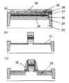
- FIG. 7 is a cross-sectional view showing a manufacturing process of the semiconductor memory element of Example 3.
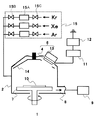
- FIG. 1 is a schematic view showing a film forming apparatus used for carrying out a method for forming a metal oxide insulating film according to the present invention.
- a film forming apparatus 1 of this embodiment includes a vacuum chamber (chamber) 2 that can be evacuated as a processing chamber, and physical vapor deposition (PVD: Physical Vapor Deposition or sputtering film formation) on a substrate 10.
- Device also called. That is, the film forming apparatus 1 of the present embodiment introduces a sputtering gas (a gas used for sputtering film formation) into the vacuum vessel 2 and applies a high voltage to cause the cations of the sputtering gas to collide with the target. A target material is sputtered to form a metal oxide insulating film on the substrate 10.
- a sputtering gas a gas used for sputtering film formation
- An exhaust device 9 such as an exhaust pump is connected through an exhaust port 8 of the vacuum vessel 2.
- a gas introduction system 15 having a flow rate controller 15A and valves 15B, 15C, etc. is connected to the vacuum vessel 2 as means for introducing the sputtering gas, and the sputtering gas is introduced from the gas introduction system 15 at a predetermined flow rate. Is done.
- a gas containing a rare gas having an atomic weight of at least krypton (Kr) among the group 18 elements in the long periodic table is introduced.
- Kr or xenon (Xe) is used alone, and argon (Ar) or the like is mixed and supplied into the vacuum vessel 2 as necessary.
- the vacuum vessel 2 has a pressure measurement mechanism (not shown), a process pressure measurement mechanism (not shown), and a partial pressure measurement mechanism (not shown).
- the pressure measurement mechanism can measure the pressure in the chamber.
- the process pressure measuring mechanism can measure pressure during the process.
- the partial pressure measuring mechanism can measure the partial pressure of various gas components such as oxygen.
- An ion gauge or the like can be used as the pressure measuring mechanism.
- As the process pressure measuring mechanism a mechanism corresponding to the process pressure such as a diaphragm gauge can be used.
- a partial pressure measuring device using quadrupole mass spectrometry and other partial pressure measuring devices can be used as appropriate. *
- a substrate holder 7 that holds the substrate 10 is disposed at the bottom of the vacuum vessel 2, and the target 4 supported by the cathode electrode 6 is disposed at the top.
- the substrate holder 7 is, for example, a disc-shaped holding table.
- the substrate holder 7 places the substrate 10 on the upper surface (front surface), and the substrate 10 is held with its processing surface facing upward. .
- the substrate holder 7 can be rotated in the in-plane direction of the substrate 10 by a rotation mechanism (not shown) such as a motor.
- the substrate holder 7 includes a heating mechanism (not shown) such as a heater.
- the substrate 10 is, for example, a semiconductor wafer, and is held by the substrate holder 7 in a state of only the substrate or mounted on a tray.
- the cathode electrode 6 is connected to a high frequency power supply 12 via a matching unit 11 as a discharge power supply for supplying a high voltage, for example.
- a magnet unit 13 for magnetron discharge is provided in the main body of the cathode electrode 6.
- the magnet unit 13 is connected to a rotation mechanism (not shown), is rotatable along the in-plane direction of the cathode electrode 6, and forms a magnetic flux parallel to the cathode surface.
- the target 4 is formed of a metal oxide containing at least one metal element having an atomic weight heavier than that of the rare gas.
- the top of the vacuum vessel 2 is provided with a shutter mechanism 14 rotatably supported by a rotation mechanism (not shown), and the front surface of the target 4 is opened and closed by a rotation operation of the shutter mechanism 14.
- a gate valve (not shown) for opening and closing the transfer path of the substrate 10 onto the substrate holder 7 is provided on the side wall of the vacuum vessel 2.
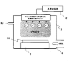
- FIG. 2 is a schematic view showing the concept of the method for forming an insulating film according to the present invention.
- a metal oxide target containing at least one metal element having an atomic weight heavier than the rare gas is installed as a target 4 in the vacuum vessel 2. Then, the inside of the vacuum vessel 2 is exhausted to a predetermined degree of vacuum by the exhaust device 9 through the exhaust port 8.
- a gate valve (not shown) on the side wall of the vacuum vessel 2 is opened, and the substrate 10 is transferred to the upper surface (front surface) of the substrate holder 7 using a transfer arm (not shown) such as a robot arm. After holding the substrate 10 on the substrate holder 7, the transfer arm is retracted and the gate valve is closed.
- sputtering gas is introduced into the vacuum vessel 2 from the gas introduction system 15.
- an oxygen-containing gas such as O 2 is not mixed with the sputtering gas.
- a gas having a high purity (usually about 99.999%) that is usually used in physical vapor deposition (PVD) is used.
- PVD physical vapor deposition
- a gas containing a rare gas having an atomic weight of at least Kr or more, for example, Kr among the Group 18 elements of the long periodic table, for example, Kr is introduced at a predetermined flow rate.
- the oxygen partial pressure of the vacuum vessel 2 is set to 1 ⁇ 10 ⁇ 6 Pa or less.
- the power supply from the high frequency power source 12 is stopped. Further, the introduction of the sputtering gas from the gas introduction system 15 is stopped, the front of the target 4 is closed by the turning operation of the shutter mechanism 14, and the inside of the vacuum vessel 2 is exhausted by the exhaust device 9.
- a transfer arm (not shown) is inserted, and the substrate 10 is unloaded from the vacuum chamber 2. Finally, the gate valve is closed to complete the entire process.
- a metal oxide insulating film containing at least one metal element having an atomic weight heavier than the introduced rare gas is formed on the substrate by PVD using a metal oxide target.
- a gas containing a rare gas having an atomic weight of at least Kr or more among the group 18 elements of the long periodic table is used as a sputtering gas, and the leakage current of the insulating film is formed by film formation in a non-oxidizing atmosphere. And based on the finding that the hysteresis is improved and the EOT does not increase.
- This ratio that is, the resputtering rate, is a function of ATOMIC MASS PARAMETER represented by the following formula when the atomic weight of the target constituent atom is Massstart and the atomic weight of the sputtering gas is Massgas (see DW Hoffman, J. et al. Vac.Sci.Technol.A8, 3707 (1990) “Intrinsic reporting-theory and experience”).
- ATOMIC MASS PARAMETER (Mastarget-Massgas) / (Maststart + Massgas)
- the target material is an atom heavier than Ar, such as La (atomic weight 138.906) and Hf (atomic weight 178.49)
- Kr atomic weight 83.798
- Ar atomic weight 39.948
- the resputtering rate is about 11%.
- the target material is La and the sputtering gas is Kr
- the resputtering rate is about 6%. From the above, when the sputtering gas is Kr, the resputtering rate is about half that of Ar.
- the resputtering rate of the deposited film due to the reflected atoms increases as the target material atoms are heavier than the sputtering gas. It is.
- a low resputtering rate is considered to indicate that the density of the deposited film is high and a desired film can be formed. If the density of the film is low, there is a problem that when a voltage is applied, vacancies (vacant sites of atoms generated by resputtering) in the film are lined up to create a path through which a current flows, and the current easily flows.
- the resputtering rate can be lowered by using Kr as the sputtering gas. Therefore, when a metal oxide insulating film containing at least one metal element having an atomic weight heavier than the sputtering gas is formed by PVD using a metal oxide target, even if Xe is used as the sputtering gas, Ar and In comparison, the electrical characteristics of the deposited film can be dramatically improved.
- the atomic weight of the sputtering gas atom and the target material atom are close to each other, or if the atomic weight of the target material atom is lighter than the sputtering gas atom, there is a difference in the weight of the target material atom.
- the effect on the resputtering rate is reduced. That is, the use of a heavy rare gas such as Kr or Xe as the sputtering gas is more effective than the formation of SiO 2 or Al 2 O 3 which is an oxide of an element lighter than Kr, for example, an element lighter than Ar. It is considered that the method is particularly effective for forming an insulating film containing a heavy element such as Hf or Hf.
- a metal oxide target containing other elements heavier than heavier rare gases such as Kr and Xe, for example, if the rare gas is Kr, Hf, La, Zr, Dy, Y, Ta, Ce, This is effective when Pr or the like is included in the target material. Further, if the rare gas is Xe, it is effective when Hf, La, Dy, Ta, Ce, Pr, etc. are included in the target material.
- FIG. 2 illustrates the case where the target 4 is parallel to the substrate 10, but when the target 4 is disposed obliquely above the substrate 10 as shown in FIG. 1, the target diameter may be small. It is more preferable because the cost can be reduced.
- the non-oxidizing atmosphere means that the sputtering gas does not contain an oxygen-containing gas such as O 2 . More specifically, the oxygen partial pressure in the film forming atmosphere of the vacuum vessel 2 is 1 ⁇ 10 ⁇ 6 Pa or less.
- the oxygen partial pressure in the film forming atmosphere of the vacuum vessel 2 is 1 ⁇ 10 ⁇ 6 Pa or less.
- EOT increases.
- the sputtered particles of the oxide material sputtered from the target are not necessarily atomic but have a considerable number of clusters.
- Example 1 describes a case where hafnium lanthanum oxide, which is a high dielectric constant film, is formed using Kr as a sputtering gas in the film forming method according to the present invention.
- Example 1 the film forming apparatus 1 shown in FIG. 1 is used, and this film forming apparatus 1 further includes a control device 16 shown in FIG.
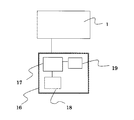
- FIG. 3 is a block diagram illustrating the film forming apparatus and the control apparatus according to the first embodiment.
- the film forming apparatus 1 includes a vacuum container 2 that can be evacuated, an exhaust system apparatus 9 that exhausts the inside of the vacuum container 2 through an exhaust port 8, a gas introduction system 15 that introduces a predetermined gas into the vacuum container 2, It has.
- a cathode electrode 6 including a target 4 provided with a surface to be sputtered exposed, a substrate holder 7 for holding a substrate 10 at a predetermined position where sputtered particles emitted from the target 4 reach, It has.
- the gas introduction system 15 is configured such that Ar gas can be introduced for Kr, Xe, and comparative experiments.
- a magnetic unit 13 for realizing magnetron sputtering is disposed in the main body of the cathode electrode 6.
- the cathode electrode 6 including the target 4 is installed obliquely above the substrate 10.
- the cathode electrode 6 is connected to a high frequency power source 12 for applying sputtering discharge power to the target 4 and a matching unit 11.
- the shutter mechanism 14 opens and closes between the target 4 and the substrate 10 by the rotation operation. At the time of film formation, the shutter mechanism 14 is opened.
- the control device 16 is formed by a computer, and the computer includes a CPU (Central Processing Unit) 17, a storage device 18 storing a control program, and an input device 19 for inputting setting information and the like.
- the computer 16 is electrically connected to and can communicate with a control element of the film forming apparatus 1, and transmits an operation command necessary for film formation to the film forming apparatus 1.
- a widely used personal computer (PC) having a predetermined performance can be used.
- the CPU 17 performs control of various control elements and various arithmetic processes according to the control program.
- Examples of the storage device 18 include a mask ROM and a hard disk (HDD).
- the ROM stores various programs and parameters for controlling the basic operation of the film forming apparatus.
- the RAM temporarily stores programs and data as a work area.
- the HDD stores various programs, parameters, and data.
- various computer-readable recording media such as a compact disk such as a CD-ROM and a CD-R, a magneto-optical disk (MO), a floppy (registered trademark) disk (FD), and a flash memory are used.
- the input device 19 can use any other input means such as a keyboard, a mouse, a touch panel, and voice input.
- the storage device 18 stores an algorithm for executing the metal oxide insulating film forming method according to the present invention as a control program.
- the control program is mounted as a mask ROM or used by being installed from a recording medium in the HDD.
- the control program includes a procedure for introducing a gas containing a rare gas having an atomic weight of Kr or more into the vacuum vessel 2 and applying a high voltage to generate plasma, and a metal element having an atomic weight heavier than the rare gas. Performing a procedure of exposing the metal oxide target to the plasma.
- the input device 19 inputs a command to the CPU 17 such as execution of a control program.
- the CPU 17 reads the control program from the storage device 18 and executes it.
- the film forming apparatus 1 is controlled based on a program execution command, and a plasma is generated in the presence of a gas containing a rare gas having an atomic weight of Kr or more, and a metal element having an atomic weight heavier than the rare gas is included in the plasma. And a step of exposing the metal oxide target comprising.
- the cathode electrode 6 in the vacuum vessel 2 has La 2 O 3 and HfO 2 containing metal elements (La, Hf) having a heavier atomic weight than the introduced rare gas as the target 4 in a 1: 2 (molar ratio).
- La 2 Hf 2 O 7 formed in 1 was installed.
- the gate valve (not shown) of the vacuum vessel 2 is opened, the substrate 10 is loaded into the vacuum vessel 2 using a transfer arm (not shown), and placed on the substrate holder 7. After holding the substrate 10 on the substrate holder 7, the transfer arm is retracted and the gate valve is closed. Further, the exhaust system device 9 exhausts the pressure in the vacuum vessel 2 until it becomes 5 ⁇ 10 ⁇ 6 Pa or less. At this time, when the oxygen partial pressure value of the vacuum vessel 2 was measured by the partial pressure measuring mechanism, it was 1 ⁇ 10 ⁇ 9 Pa.
- a gas containing a rare gas having an atomic weight of at least Kr or more is introduced as a sputtering gas.
- a high frequency voltage is applied from the high frequency power source 12 to the target 4 while introducing the sputtering gas from the gas introduction system 15, sputter discharge occurs in the space where the target 4 faces and the target 4 is sputtered by the self-bias voltage.
- hafnium lanthanum oxide hereinafter referred to as “LaHfO film” is formed on the surface of the substrate 10.
- the LaHfO film used as the name of the film is not related to the composition ratio of elements in the film. (Also for other films) films are deposited.
- the substrate holder 7 is rotated by a rotation mechanism (not shown), and the substrate 10 is rotated with respect to the stationary target 4.
- the LaHfO film formed on the substrate 10 becomes a uniform film.
- the La 2 Hf 2 O 7 target was supplied with 300 W of high-frequency power (frequency of 13.56 MHz).
- An insulating film of LaHfO having a thickness of 20 nm was formed on a silicon substrate having a specific resistance of 8 to 12 ⁇ ⁇ cm at a pressure of 0.1 Pa by introducing Ksc gas having a purity of 99.999% as a sputtering gas.
- Ksccm is an abbreviation for standard cc per minute, and is a unit of gas flow rate supplied per minute in terms of cm 3 at 0 ° C. and 1 atm, which is the standard state.
- the oxygen partial pressure during film formation by the partial pressure measuring mechanism was 1 ⁇ 10 ⁇ 7 to 1 ⁇ 10 ⁇ 8 Pa.
- Ar gas of 140 sccm having a purity of 99.9999% was introduced to a pressure of 0.1 Pa, and similarly, 20 nm LaHfO was applied onto a silicon substrate having a specific resistance of 8 to 12 ⁇ ⁇ cm. An insulating film was formed.
- an Al pad having a diameter of 1 mm was deposited as an upper electrode on the formed LaHfO film by an evaporation method using a mask for measuring electrical characteristics. In was used as the lower electrode.
- FIG. 4 is an explanatory diagram showing current-voltage characteristics of the LaHfO film obtained by the above film forming method.
- the leakage current density is lower when the sputter deposition is performed using Kr gas than when the sputtering deposition is performed using Ar gas.
- the leakage current density when sputtering with Ar gas is 7.4 ⁇ 10 ⁇ 9 [A / cm 2 ], compared with 7.4 ⁇ 10 ⁇ 9 [A / cm 2 ].
- the film was formed, it was 1.4 ⁇ 10 ⁇ 9 [A / cm 2 ], which was as low as about 1/5.
- FIG. 5 is an explanatory diagram showing capacitance-voltage characteristics of the LaHfO film of FIG.
- the width of the hysteresis is narrower when the sputter film is formed with Kr gas than when the sputter film is formed with Ar gas. That is, in FIG. 5, the hysteresis width in the case of the conventional Ar is 0.4V, whereas Kr is 0.28V, and as a result, the hysteresis is improved to about 70% of Ar in Kr. .
- Example 2 In the second embodiment, a case where Xe is used as a sputtering gas and hafnium lanthanum oxide which is a high dielectric constant film is formed in the method for forming an insulating film according to the present invention will be described.
- Example 2 the same apparatus as in Example 1 was used, and the film was formed under the same procedure and the same conditions except for the sputtering gas. That is, 300 W of high-frequency power (frequency: 13.56 MHz) was input to the La 2 Hf 2 O 7 target. An Xe gas having a purity of 99.9999% was introduced as a sputtering gas to a pressure of 0.1 Pa, and a 20 nm LaHfO insulating film was formed on a silicon substrate having a specific resistance of 8 to 12 ⁇ ⁇ cm.
- high-frequency power frequency: 13.56 MHz
- An Xe gas having a purity of 99.9999% was introduced as a sputtering gas to a pressure of 0.1 Pa, and a 20 nm LaHfO insulating film was formed on a silicon substrate having a specific resistance of 8 to 12 ⁇ ⁇ cm.
- FIG. 6 is a cross-sectional view showing a manufacturing process of the semiconductor memory device of Example 3.
- the semiconductor memory device of this embodiment includes a substrate having at least a surface composed of a semiconductor layer, a gate electrode formed on the substrate, and a stacked gate insulating layer sequentially stacked between the substrate and the gate electrode. And a membrane.
- the metal oxide insulating film constituting at least one layer of the stacked gate insulating film is stacked by using the metal oxide insulating film forming method according to the present invention.
- an element isolation layer 24 was formed on the surface of the silicon substrate 23 using STI (Shallow Trench Isolation) technology.
- a silicon oxide film 25 having a thickness of 30 to 100 mm is formed as a first insulating film on the element-isolated silicon substrate 23 by a thermal oxide film method.
- a silicon nitride film 26 having a thickness of 30 to 100 mm is formed as a second insulating film by LPCVD (Low Pressure Chemical Vapor Deposition) method.
- an aluminum oxide film 27 having a thickness of 5 to 50 mm is formed as a third insulating film.
- MOCVD Metal Organic Chemical Vapor Deposition
- ALD Advanced Deposition
- PVD Physical Vapor Deposition
- LaHfO film 28 having a thickness of 10 to 200 mm is formed as a fourth insulating film.
- the formation of LaHfO is the same as the formation conditions of Example 1 and Example 2.
- an aluminum oxide film 29 having a thickness of 5 to 50 mm is formed as a fifth insulating film.
- a film formation method an MOCVD method, an ALD method, or a PVD method is used.
- a poly-Si film 30 having a thickness of 150 nm was formed on the aluminum oxide film 29 as a gate electrode.
- the gate electrode is processed using lithography technology and RIE (Reactive Ion Etching) technology, and then ion implantation is performed, and the gate electrode is self-processed using the extension diffusion region 31 as a mask. Consistently formed.
- RIE Reactive Ion Etching
- a gate side wall 32 was formed by sequentially depositing a silicon nitride film and a silicon oxide film and then etching back. In this state, ion implantation was performed again, and source / drain diffusion layers 33 were formed through activation annealing.
- a poly-Si film is used as the gate electrode.
- the same effect can be obtained by using TiN, TaN, W, WN, Pt, Ir, Pt, Ta, Ti as the gate electrode. did it.
- the first insulating film, the second insulating film, the third insulating film, the fourth insulating film, and the fifth insulating film are annealed by activation annealing after ion implantation.
- annealing may be performed after each insulating film is formed.
- a stacked insulating film of the third insulating film, the fourth insulating film, and the fifth insulating film is used as the blocking layer of the nonvolatile semiconductor memory element.
- a stacked insulating film of the third insulating film, the fourth insulating film, and the fifth insulating film is used as the blocking layer of the nonvolatile semiconductor memory element.
- the same effect could be obtained with a laminated insulating film of the film and the fourth insulating film.
- the method for forming a metal oxide insulating film of the present invention can be widely applied to the manufacture of nonvolatile semiconductor memory elements.
Landscapes
- Chemical & Material Sciences (AREA)
- Chemical Kinetics & Catalysis (AREA)
- Engineering & Computer Science (AREA)
- Materials Engineering (AREA)
- Mechanical Engineering (AREA)
- Metallurgy (AREA)
- Organic Chemistry (AREA)
- Physical Vapour Deposition (AREA)
- Semiconductor Memories (AREA)
- Formation Of Insulating Films (AREA)
- Non-Volatile Memory (AREA)
Abstract
不揮発性半導体メモリ素子向けの絶縁膜形成において、リーク電流密度を低減でき、デバイス特性及び信頼性を向上させることができる金属酸化物絶縁膜の成膜方法を提供する。 Kr以上の原子量を有する希ガスを導入して、導入希ガスより重い金属元素を含む金属酸化物ターゲットを用い、LaHfO、LaAlO、ZrAlOのように導入希ガスより重いLaまたはHfなどの金属元素を含む金属酸化物絶縁膜をスパッタ成膜する。
Description
本発明は、真空容器内にスパッタガスを導入し、高電圧を印加してスパッタガスのイオンをターゲットに衝突させてターゲット物質をスパッタし、基板上に金属酸化物絶縁膜を成膜する方法に関する。さらに本発明は、金属酸化物絶縁膜の成膜方法を用いて製造する不揮発性半導体メモリ素子及びその製造方法、成膜装置の制御プログラム、並びに記録媒体に関する。
不揮発性半導体メモリ素子は、電荷捕獲手段として、FG(Floating Gate)型と、MONOS(Metal Oxide Nitride Oxide Semiconductor)型と、がある。
FG型は、電荷蓄積層として、ゲート絶縁膜中に埋め込まれたポリシリコン等の導電性の膜を使用する。FG型はポリシリコン等を用いるため、ゲート絶縁膜とのエネルギー障壁が大きく、捕獲された電荷の半導体基板表面やゲート電極側へのリークが少ない。
一方、MONOS型は、ゲート絶縁膜中に積層されたシリコン窒化膜などの絶縁性の膜を使用する。MONOS型は、積層されたゲート絶縁膜中に電荷を蓄積するため、エネルギー障壁が小さい。従って、一般にFG型は、MONOS型よりも高温における記憶保持特性が優れる。
しかしFG型は、電荷保持能力の点で、FG部と半導体基板表面の間のシリコン酸化膜の薄膜化に課題がある。即ち、10nm以下のシリコン酸化膜にFNトンネル注入すると、SILC(Stress Induced Leakage Current)と呼ばれる低電界領域でのリーク電流が発生し、FGに蓄積された電荷がこのリークパスを通って全て失われる。従って、FG型におけるトンネル酸化膜の薄膜化は、SILC発生のため、8nmが電荷保持能力の観点から下限となる。よってFG型は、微細化による動作電圧の低減と保持能力の維持との両立が困難である。
これに対して、MONOS型では、電荷の蓄積を担う電荷捕獲サイトがそれを含む絶縁膜中に空間的に離散化して存在している。そのため、FG型と同様なSILCによるリークパスが発生しても、リークパス周辺の局所的な電荷が失われるだけであり、素子全体の不揮発性の消失には至らない。従って、MONOS型は、電荷保持層と半導体基板表面の間のシリコン酸化膜の薄膜化が可能となり、結果として、FG型と比較して薄膜化による素子の動作電圧の低減ができる。
近年、上述した微細化の観点から、半導体メモリ素子の更なる高集積化を目的として、MONOS型の不揮発性半導体メモリ素子が注目されている。
MONOS型は、一般的に半導体基板の表面側から第1の絶縁膜としてシリコン酸化膜、第2の絶縁膜としてシリコン窒化膜、及び第3の絶縁膜としてシリコン酸化膜を積層した構造を有する。第1のシリコン酸化膜は、蓄積された電荷の半導体基板へのリークを防止する機能を有する。第2のシリコン窒化膜は、電荷蓄積層として機能する。第3のシリコン酸化膜は、ブロッキング層として、蓄積された電荷のゲート電極側へのリークを防止する機能を有する。
このMONOS型半導体不揮発メモリ素子の微細化に伴って、ブロッキング層として高誘電率を有する絶縁膜を適用することが望まれており、シリコン酸化膜よりも比誘電率が大きいゲート絶縁膜の適用が検討されている。このシリコン酸化膜より比誘電率が大きい絶縁膜を高誘電率膜と呼ぶ。
ここで、酸化膜換算膜厚について説明する。ゲート絶縁膜の種類によらず、ゲート絶縁膜材料がシリコン酸化膜であると仮定して、ゲート容量から逆算して得られる絶縁膜の電気的な膜厚をシリコン酸化膜換算膜厚(EOT:Equivalent Oxide Thickness)という。即ち、絶縁膜の比誘電率をεh、シリコン酸化膜の比誘電率をεoとし、絶縁膜の厚さをdhとしたとき、シリコン酸化膜換算膜厚deは、de=dh×(εo/εh)で表される。
上記数式は、ゲート絶縁膜に、シリコン酸化膜の比誘電率εoに比べて大きな誘電率εhをもった材料を用いた場合には、シリコン酸化膜の換算膜厚は、このゲート絶縁膜の膜厚よりも薄いシリコン酸化膜と同等になることを示している。なお、シリコン酸化膜の比誘電率εoは3.9程度である。そのため、例えば、εh=39の高誘電率材料からなる膜は、その物理膜厚を15nmとしても、シリコン酸化膜換算膜厚(電気膜厚)が1.5nmになる。従って、ゲート絶縁膜の容量値を膜厚が1.5nmのシリコン酸化膜と同等に保ちつつ、トンネル電流を著しく低減することができる。よって、ブロッキング層に高誘電率膜を適用することにより、リークによる保持特性の劣化を招くことなく、EOTの薄膜化による動作電圧の低減が可能となる。高誘電率膜の成膜方法として、CVD(Chemical Vapor Deposition)法、原子層吸着堆積法、スパッタ法が挙げられる。CVD法は、形成過程においてインキュベーションタイムが存在するため、膜厚の制御性、面内均一性、及び再現性が課題となる。一方、スパッタ法は絶縁膜へのプラズマダメージによる下地の酸化や界面層の形成が課題となる。このスパッタ法による高誘電率膜の形成には、スパッタガスにArとO2などの反応性ガスとの混合ガスを用いた反応性スパッタが用いられている。
例えば、特許文献1には、ArとO2の混合ガスを用い、膜厚20nmの酸化タンタル膜を成膜する技術が提案されている。
また、特許文献2には、高周波(RF:Radio Frequency)電力を用いたスパッタ装置で酸化物のターゲットを用い、スパッタガスとして酸素含有ガスを添加しないArガスだけを導入して、絶縁膜の成膜を行なう技術が提案されている。
また、特許文献3には、メタルターゲットの背面に磁石を備え、イオン化率を高めるためターゲットにRFコイルを備え、ターゲットに対向する基板を有するマグネトロンスパッタ装置が提案されている。このマグネトロンスパッタ装置は、金属膜の成膜と酸化による金属膜の絶縁化合物化とを交互に行って、絶縁膜を成膜する。
ところで、上述した絶縁膜の成膜方法には、以下のような課題が存在する。即ち、特許文献1の方法では、ArとO2ガスの混合ガスを用いているため、絶縁膜の下地(絶縁膜の下層や基板)が酸化され、EOTが増大するという問題がある。
このような下地の酸化の問題は、例えば、特許文献2のようにスパッタガスに酸素含有ガスを添加せずArガスだけを導入する方法で回避することができる。しかし、ターゲットを構成する元素の下地基板への打ち込みによりトラップが形成されるため、容量-電圧特性にヒステリシスが発生し、デバイス特性のばらつきや信頼性が低下するという問題がある。
また、特許文献3の成膜方法においても、ターゲットを構成する元素の下地基板への打ち込みによりトラップが形成され、デバイス特性が悪化するという問題がある。
このように、従来の絶縁膜の成膜方法では、近年の不揮発性メモリ素子の絶縁膜に要求される低いリーク電流密度と界面におけるトラップ形成によるデバイス特性の悪化を抑制することが困難であった。
本発明は、上記事情に鑑み、リーク電流密度を低減することができ、ヒステリシスを改善してデバイス特性及び信頼性を向上させることができる金属酸化物絶縁膜の成膜方法を提供することを目的とする。また、本発明に係る金属酸化物絶縁膜の成膜方法を用いて製造する不揮発性半導体メモリ素子及びその製造方法、成膜装置の制御プログラム、並びに記録媒体を提供することを目的とする。
上記の目的を達成すべく成された本発明の構成は以下の通りである。
即ち、真空容器の内部にスパッタガスを導入し、高電圧を印加してスパッタガスのイオンをターゲットに衝突させてターゲット物質をスパッタし、基板の上に金属酸化物絶縁膜を成膜する方法において、上記スパッタガスとして、少なくともKr以上の原子量を有する希ガスを含むガスを導入し、プラズマを生成する手順と、上記プラズマに、上記希ガスより重い原子量を有する金属元素を含む金属酸化物のターゲットを曝し、上記希ガスより重い原子量を有する金属元素を少なくとも1つ含む金属酸化物絶縁膜を成膜する手順と、を有することを特徴とする金属酸化物絶縁膜の成膜方法である。
本発明によれば、スパッタガスとしてKr以上の原子量を有する希ガスを導入し、高電圧を印可してプラズマを生成し、上記希ガスよりも重い原子量を有する金属元素を含む金属酸化物のターゲットを使用する場合、再スパッタ率を下げることができる。従って、従来のArを用いた絶縁膜のスパッタ成膜に比して、下地の酸化によるEOTの増加を招くことなく、リーク電流密度を低減できる。また、ヒステリシスを改善して、デバイス特性及び信頼性を向上させることができる。
1 成膜装置
2 真空容器
4 ターゲット
6 カソード電極
10 基板
12 高周波電源
13 磁石ユニット
15 ガス供給系
16 制御装置
18 記憶装置
23 シリコン基板
24 素子分離領域
25 第1の絶縁膜
26 第2の絶縁膜
27 第3の絶縁膜
28 第4の絶縁膜
29 第5の絶縁膜
30 ゲート電極
2 真空容器
4 ターゲット
6 カソード電極
10 基板
12 高周波電源
13 磁石ユニット
15 ガス供給系
16 制御装置
18 記憶装置
23 シリコン基板
24 素子分離領域
25 第1の絶縁膜
26 第2の絶縁膜
27 第3の絶縁膜
28 第4の絶縁膜
29 第5の絶縁膜
30 ゲート電極
以下、図面を参照して、本発明の実施の形態を説明するが、本発明は本実施形態に限定されるものではない。
図1は、本発明に係る金属酸化物絶縁膜の成膜方法の実施に用いる成膜装置を示す模式図である。
図1に示すように、本実施形態の成膜装置1は、処理室として真空排気可能な真空容器(チャンバ)2を備え、基板10上に物理蒸着(PVD:Physical Vapor Deposition、あるいはスパッタ成膜とも呼称される)する装置である。即ち、本実施形態の成膜装置1は、真空容器2の内部にスパッタガス(スパッタ成膜に使用するガス)を導入し、高電圧を印加してスパッタガスの陽イオンをターゲットに衝突させてターゲット物質をスパッタし、基板10上に金属酸化物絶縁膜を成膜する。
真空容器2の排気ポート8を介して排気ポンプ等の排気装置9が接続されている。また、真空容器2には、スパッタガスの導入手段として、流量制御器15Aやバルブ15B、15Cなどを備えたガス導入系15が接続され、このガス導入系15からスパッタガスが所定の流量で導入される。本実施形態のスパッタガスとしては、長周期律表の第18族元素のうち、少なくともクリプトン(Kr)以上の原子量を有する希ガスを含むガスを導入する。Kr以上の原子量を有する希ガスとしては、例えば、Krまたはキセノン(Xe)を単独使用し、必要に応じてアルゴン(Ar)等を混合して真空容器2内に供給する。
真空容器2には、不図示の圧力測定機構、不図示のプロセス圧力測定機構、そして不図示の分圧測定機構がある。圧力測定機構はチャンバー内の圧力測定を行なえるようになっている。プロセス圧力測定機構はプロセス中の圧力測定を行なえるようになっている。分圧測定機構は酸素などの各種気体成分の分圧の測定を行なえるようになっている。圧力測定機構としてはイオンゲージなどが使用できる。プロセス圧力測定機構としてはダイアフラムゲージ等のプロセス圧力に応じたものが使用できる。分圧測定機構としては、四重極型質量分析を利用した分圧測定器や、その他の分圧測定装置を適宜使用することができる。
本実施形態の成膜装置1は、真空容器2の下部に基板10を保持する基板ホルダ7を配置しており、上部にカソード電極6に支持されたターゲット4を配置している。
基板ホルダ7は、例えば、円板状の保持テーブルであって、基板ホルダ7は、その上面(表面)に基板10を載置し、基板10はその処理面を上方へ臨ませて保持される。基板ホルダ7は、モータ等の不図示の回転機構により、基板10の面内方向に回転可能となっている。なお、基板ホルダ7には、ヒータ等の不図示の加熱機構が内蔵されている。
基板10としては、例えば、半導体ウエハが挙げられ、基板のみの状態もしくはトレイに搭載された状態で、基板ホルダ7に保持される。
カソード電極6には、高電圧を供給する放電用電源として、例えば、整合器11を介して高周波電源12が接続されている。このカソード電極6の本体内には、マグネトロン放電用の磁石ユニット13が備えられている。磁石ユニット13は、不図示の回転機構に接続され、カソード電極6の面内方向に沿って回転可能と成っており、カソード表面に平行な磁束を形成する。
本実施形態では、ターゲット4として、上記希ガスよりも重い原子量を有する金属元素を少なくとも1つ含む金属酸化物で形成されている。真空容器2の天部には、不図示の回転機構に回転可能に支持されたシャッタ機構14が備えられており、シャッタ機構14の回動操作によりターゲット4の前面が開閉される。
なお、真空容器2の側壁には、基板ホルダ7上への基板10の搬送経路を開閉するための不図示のゲートバルブが設けられている。
次に、本発明に係る金属酸化物絶縁膜の成膜方法について説明する。図2は、本発明に係る絶縁膜の成膜方法の概念を示す概略図である。
図1および図2を参照して、まず、真空容器2内に、ターゲット4として、上記希ガスより重い原子量を有する金属元素を少なくとも1つ含む金属酸化物ターゲットを設置する。そして、排気ポート8を通じて排気装置9により、真空容器2内を所定の真空度まで排気する。
次に、真空容器2の側壁の不図示のゲートバルブを開け、ロボットアーム等の不図示の搬送アームを用いて、基板10を基板ホルダ7の上面(表面)へと搬送する。基板ホルダ7上に基板10を保持した後、搬送アームを後退させ、ゲートバルブを閉じる。
次に、真空容器2内にガス導入系15よりスパッタガスを導入する。このとき、スパッタガスには、O2などの酸素含有ガスは混合しない。スパッタガスには、物理蒸着(PVD)で通常使用される程度の高純度(多くは99.999%程度)のガスを使用する。本実施形態では、スパッタガスとして、長周期律表の第18族元素のうち、少なくともKr以上の原子量を有する希ガスを含むガス、例えば、Krを所定の流量だけ導入する。このとき、真空容器2の酸素分圧は1×10⁻⁶Pa以下とする。
次に、このスパッタガスの導入下において、回転機構によって磁石ユニット13を回転させながら、カソード電極6に高周波電源12から放電用電力を投入する。カソード電極6に高電圧を印可すると、カソード電極6と基板ホルダ7との間でマグネトロン放電が行われ、プラズマが発生する。次に、シャッタ機構14の回動操作によりターゲット4の前方を開ける。プラズマ中のKr以上の原子量を有する希ガスの陽イオンでターゲット物質がスパッタされ、基板10の処理面に上記希ガスより重い原子量を有する金属元素を少なくとも1つ含む金属酸化物絶縁膜が成膜される。その結果、従来のよりも絶縁膜のリーク電流とヒステリシスが改善され、しかもシリコン酸化膜換算膜厚(EOT)が増加しない。
基板10上に所定の膜厚を堆積後、高周波電源12からの電力供給を停止する。さらに、ガス導入系15からのスパッタガスの導入を停止し、シャッタ機構14の回動操作によりターゲット4の前方を閉じ、排気装置9により真空容器2の内部を排気する。
次に、ゲートバルブを開けた後、不図示の搬送アームを挿入し、真空容器2内から基板10を搬出する。最後に、ゲートバルブを閉じて、全工程を終了する。
本発明は、金属酸化物ターゲットを用いたPVDにより、基板上に導入希ガスより重い原子量を有する金属元素を少なくとも1つ含む金属酸化物絶縁膜を成膜する。その際、スパッタガスとして、長周期律表の第18族元素のうち、少なくともKr以上の原子量を有する希ガスを含むガスを用い、非酸化性雰囲気下での成膜により、絶縁膜のリーク電流とヒステリシスが改善され、EOTが増加しないという所見に基づいている。
これは、以下の原理に由来していると考えられる。一般に、ターゲットに電力を印加してターゲット原子を陽イオンでスパッタするとき、スパッタガスの陽イオンが衝突したターゲットからは、ターゲットを構成する原子などのスパッタ粒子と2次電子が放出される。また、ターゲットに衝突した陽イオンが電荷を失わずに反射または散乱する。さらに、ターゲットに衝突した陽イオンのうち、電荷を失って反射散乱してかなりのエネルギーをもったまま飛び出してくる希ガスの原子がある。この原子を「反射原子」と呼び、この反射原子に注目する。反射原子は高いエネルギーをもっているので、基板上の堆積膜に衝突することでその膜を再スパッタする。
この割合、即ち再スパッタ率は、ターゲット構成原子の原子量をMasstarget、スパッタガスの原子量をMassgasとしたとき、下記数式で表わされるATOMIC MASS PARAMETERの関数となる(参照;D.W.Hoffman, J.Vac.Sci.Technol.A8,3707(1990) “Intrinsic resputtering-theory and experiment”)。
ATOMIC MASS PARAMETER=(Masstarget- Massgas)/(Masstarget+ Massgas)
ターゲット材料がLa(原子量138.906)とHf(原子量178.49)のようにArよりも重い原子の場合、Ar(原子量39.948)に比べ、Kr(原子量83.798)でスパッタをすると、基板上での再スパッタ率が下がる。
例えば、ターゲット材料がランタン(La)であり、スパッタガスがArの場合は、ATOMIC MASS PARAMETER=0.553となり、D.W.Hoffmanの文献中のFig4によれば、再スパッタ率は約11%である。一方で、ターゲット材料がLaであり、スパッタガスがKrの場合には、ATOMIC MASS PARAMETER=0.247となり、再スパッタ率は約6%である。以上により、スパッタガスがKrの場合、Arの場合と比べて、半分程度に再スパッタ率が低い。
同様に、ターゲット材料がハフニウム(Hf)であり、スパッタガスがArのときのATOMIC MASS PARAMETER=0.634より再スパッタ率は約14%である。また、ターゲット材料がHfであり、スパッタガスがKrのときのATOMIC MASS PARAMETER=0.361より再スパッタ率は約7%である。従って、Hfの場合にも、Krを使用すると、Arよりも再スパッタ率を低くすることができる。
このように、スパッタガスよりも重い原子量の金属元素を含むターゲット材料を使用した場合、スパッタガスよりもターゲット材料の原子が重いほど、反射原子による堆積膜の再スパッタ率が高くなることが、明らかである。再スパッタ率が低いということは堆積膜の密度が高く、所望の膜が成膜できると考えられる。膜の密度が低いと電圧を印加した場合に膜中の空孔(再スパッタにより生成した原子の空サイト)が並んで電流が流れるパスを作り、電流が流れ易くなるという問題が発生する。
この観点から、LaHfO膜をスパッタガスにKrガスを用いて成膜した場合には、スパッタガスにArガスを用いた場合の成膜に比べ、高密度の膜ができ、リーク電流密度が低減し、ヒステリシス特性を改善することができたと考えられる。
このように、スパッタガスよりも重い原子量の金属元素を含むターゲット材料を使用した場合、スパッタガスとしてKrを使用すれば、再スパッタ率を下げることができる。従って、金属酸化物ターゲットを用いたPVDにより、スパッタガスよりも重い原子量を有する金属元素を少なくとも1つ含む金属酸化物絶縁膜を成膜する場合、スパッタガスとしてXeを使用しても、Arと比較して堆積膜の電気的特性を飛躍的に向上できる。
なお、スパッタガスの原子とターゲット材料の原子との原子量が近接しているか、又は、スパッタガスの原子よりもターゲット材料の原子の原子量が軽い場合には、ターゲット材料の原子の重さの違いが再スパッタ率に与える影響は小さくなる。即ち、KrやXeなどの重い希ガスをスパッタガスに使用することは、Krよりも軽い元素、例えば、Arよりも軽い元素の酸化物であるSiO2やAl2O3の形成よりも、LaやHfなどの重い元素を含む絶縁膜の成膜に特に効果があると考えられる。一方、KrやXeなどの重い希ガスよりも、更に重い他の元素が含まれる金属酸化物ターゲット、例えば、希ガスがKrであれば、Hf、La、Zr、Dy、Y、Ta、Ce、Prなどがターゲット材料に含まれる場合に有効である。また、希ガスがXeであれば、Hf、La、Dy、Ta、Ce、Prなどがターゲット材料に含まれる場合に有効である。
また、スパッタガスとしてKrのみを使用した場合だけでなく、KrとArの混合ガスを用いても、Krの分圧に応じて前述の電気的特性向上の効果が得られる。Krの混合量だけ、反射原子による再スパッタ率が低下するためと推測される。Xeにおいても同様である。
図2の概念図は、基板10に対してターゲット4が平行である場合について図示されているが、図1のように基板10の斜め上方にターゲット4を配置する場合、ターゲット径が小さくて済み、コストを低減できるのでより好ましい。
次に、非酸化性雰囲気下において成膜することが重要である理由について説明する。ここで、非酸化性雰囲気とは、スパッタガス中にO2などの酸素含有ガスを含まないことを意味する。さらに具体的には真空容器2の成膜雰囲気に酸素分圧が1×10⁻⁶Pa以下であることである。スパッタガスにO2などの酸素含有ガスを含む従来の反応性スパッタ法では、EOTが増加する。しかし、本発明の方法では、ターゲットからスパッタされた酸化物材料のスパッタ粒子が、必ずしも原子状のものばかりではなく、クラスター状であるものも相当数ある。非酸化性雰囲気下で成膜する結果として、EOT増加に影響する活性な原子状酸素や分子状の酸素が雰囲気中に極めて少なくなり、EOTの増加はスパッタガスにO2などの酸素含有ガスを添加した場合と比べて、殆ど問題にならないと考えられる。
以下、実施例を挙げて本発明を詳細に説明するが、本発明はこれらの実施例に限定されるものではない。
〔実施例1〕
実施例1は、本発明に係る成膜方法において、スパッタガスとしてKrを使用し、高誘電率膜である酸化ハフニウムランタンを成膜する場合について説明する。
実施例1は、本発明に係る成膜方法において、スパッタガスとしてKrを使用し、高誘電率膜である酸化ハフニウムランタンを成膜する場合について説明する。
実施例1では、図1に示した成膜装置1を用いており、この成膜装置1は更に図3に示す制御装置16を備えている。図3は、実施例1の成膜装置および制御装置を示すブロック図である。
再び図1を参照して、成膜装置1について概略説明する。成膜装置1は、真空排気可能な真空容器2を備え、排気ポート8を通じて真空容器2内を排気する排気系装置9と、真空容器2内へ所定のガスを導入するガス導入系15と、を備えている。この真空容器2内には、被スパッタ面を露出させて設けたターゲット4を含むカソード電極6と、ターゲット4から放出されたスパッタ粒子が到達する所定位置に基板10を保持する基板ホルダ7と、を備えている。
ガス導入系15には、Kr、Xe、そして比較実験などのためにArガスが導入可能なように構成されている。カソード電極6の本体内には、マグネトロンスパッタリングを実現するための磁気ユニット13が配設されている。ターゲット4を含むカソード電極6は、基板10の斜め上方に設置されている。カソード電極6には、スパッタ放電用電力をターゲット4に印加する高周波電源12と整合器11が接続されている。シャッタ機構14は、その回転操作により、ターゲット4と基板10との間を開閉する。成膜時にはシャッタ機構14は開の状態とされる。
図3を参照して、制御装置16はコンピュータにより形成され、コンピュータはCPU(中央演算装置)17と、制御プログラムを格納した記憶装置18と、設定情報等を入力する入力装置19と、から構成されている。コンピュータ16は、成膜装置1の制御要素と電気的に接続されて通信可能であり、成膜装置1に成膜に必要な動作指令を送信する。
コンピュータ16には、例えば、広く普及している所定の性能のパーソナルコンピュータ(PC)を使用することができる。
CPU17は、制御プログラムにしたがって各制御要素の制御や各種の演算処理等を行う。
記憶装置18としては、マスクROMやハードディスク(HDD)等が挙げられる。ROMは、成膜装置の基本動作を制御する各種プログラムやパラメータを格納する。RAMは、作業領域として一時的にプログラムやデータを記憶する。HDDは、各種プログラムやパラメータ、データを格納する。記録媒体としては、CD-ROM、CD-R等のコンパクトディスク、光磁気ディスク(MO)、フロッピー(登録商標)ディスク(FD)、フラッシュメモリ等のコンピュータ読み取り可能な各種記録媒体が用いられる。
入力装置19は、キーボード、マウス、タッチパネル、音声入力など、その他あらゆる入力手段が使用できる。
記憶装置18には、本発明に係る金属酸化物絶縁膜の成膜方法を実行するアルゴリズムが制御プログラムとして格納される。即ち、制御プログラムは、マスクROMとして実装されるか、HDDに記録媒体からインストールして使用される。制御プログラムは、真空容器2内に、Kr以上の原子量を有する希ガスを含むガスを導入し、高電圧を印可してプラズマを生成する手順と、上記希ガスより重い原子量を有する金属元素を含む金属酸化物ターゲットをプラズマに曝す手順と、を実行する。
入力装置19は、制御プログラムの実行などのCPU17への指令を入力する。CPU17は、記憶装置18より制御プログラムを読み出して実行する。プログラムの実行指令に基づいて成膜装置1が制御され、Kr以上の原子量を有する希ガスを含むガスの存在下でプラズマを生成する手順と、プラズマに上記希ガスより重い原子量を有する金属元素を含む金属酸化物ターゲットを曝す手順と、を実施する。
次に、上記の成膜装置1および制御装置16を用いた絶縁膜の成膜方法について説明する。真空容器2内のカソード電極6に、ターゲット4として、導入希ガスよりも重い原子量を有する金属元素(La、Hf)を含むLa2O3とHfO2を1:2(mol比)になるように形成したLa2Hf2O7を設置した。
まず、真空容器2の不図示のゲートバルブを開け、不図示の搬送アームを用いて真空容器2内に基板10を搬入し、基板ホルダ7上に載置する。基板ホルダ7上に基板10を保持した後、搬送アームを後退させ、ゲートバルブを閉じる。さらに、排気系装置9により、真空容器2内の圧力を5×10⁻⁶Pa以下になるまで排気する。このとき、分圧測定機構により真空容器2の酸素分圧値を計測したところ1×10⁻⁹Paであった。
次に、スパッタガスとして、少なくともKr以上の原子量を有する希ガスを含むガスを導入する。スパッタガスをガス導入系15から導入しながら、高周波電源12からターゲット4に高周波電圧を印加すると、ターゲット4が臨む空間にスパッタ放電が生じ、セルフバイアス電圧によりターゲット4がスパッタされる。その結果、基板10の表面に、酸化ハフニウムランタン(以下、「LaHfO膜」と呼ぶ。なお、本明細書において、膜の名称として使用するLaHfO膜の表記と膜中元素の組成比とは無関係である。また、他の膜に関しても同様である)膜が堆積される。
この成膜の間、不図示の回転機構により基板ホルダ7を回転させ、静止したターゲット4に対して基板10を回転させる。これにより、基板10上に作成されるLaHfO膜は均一な膜となる。基板10に対して斜方に設置したターゲット4から、スパッタ粒子を飛来させて成膜しながら基板10を回転させる本成膜装置1を使用することで、極めて均一で良質な膜を得ることができる。
次に、成膜条件について説明する。La2Hf2O7ターゲットには、300Wの高周波電力(周波数が13.56MHz)を投入した。スパッタガスとして純度99.999%のKrガス110sccmを導入し、0.1Paの圧力とし、比抵抗が8~12Ω・cmのシリコン基板上へ20nmのLaHfOの絶縁膜を成膜した。なお、sccmは、standard cc per minuteの略であり、標準状態である0℃1気圧のcm3単位に換算した1分間あたり供給するガス流量の単位である。なお、分圧測定機構による成膜中の酸素分圧値は、1×10⁻⁷~1×10⁻⁸Paであった。
また、本実施例との比較のために、純度99.9999%のArガス140sccmを導入し、0.1Paの圧力とし、同様に比抵抗が8~12Ω・cmのシリコン基板上へ20nmのLaHfOの絶縁膜を成膜した。
その後、成膜したLaHfO膜は電気特性測定のため、マスクを使用した蒸着法により、上部電極として直径1mmのAlパッドを堆積させた。下部電極としてはInを用いた。
図4は、上記の成膜方法で得たLaHfO膜の電流-電圧特性を示す説明図である。図4に示すように、Arガスでスパッタ成膜した場合に比べて、Krガスでスパッタ成膜した場合にリーク電流密度が低くなっていることが判る。特に、5[-MV/cm]のときに、Arガスでスパッタ成膜した場合のリーク電流密度は7.4×10-9[A/cm2]であるのに比べ、Krガスでスパッタ成膜した場合は1.4×10-9[A/cm2]であり、およそ5分の1と低くなった。
次に、図5は、図4のLaHfO膜のキャパシタンス-電圧特性を示す説明図である。図5に示すように、Arガスでスパッタ成膜した場合に比べて、Krガスでスパッタ成膜した場合は、ヒステリシスの幅が狭くなることが判る。即ち、図5において、従来のArの場合のヒステリシスの幅が0.4Vであるのに対して、Krでは0.28Vであり、結果としてKrではArの70%程度にヒステリシスが改善されていた。
また、従来のArとO2の混合ガスを用いた絶縁膜のスパッタ成膜のように、下地を酸化してEOTが増加するという問題も生じなかった。
〔実施例2〕
実施例2では、本発明に係る絶縁膜の成膜方法において、スパッタガスとしてXeを使用し、高誘電率膜である酸化ハフニウムランタンを成膜する場合について説明する。
実施例2では、本発明に係る絶縁膜の成膜方法において、スパッタガスとしてXeを使用し、高誘電率膜である酸化ハフニウムランタンを成膜する場合について説明する。
本実施例では、実施例1と同じ装置を使用し、スパッタガス以外は同じ手順、同じ条件で成膜した。即ち、La2Hf2O7ターゲットには、300Wの高周波電力(周波数が13.56MHz)を投入した。スパッタガスとして純度99.9999%のXeガスを導入して0.1Paの圧力とし、比抵抗が8~12Ω・cmのシリコン基板上へ20nmのLaHfOの絶縁膜を成膜した。
実施例1と同様の方法にて、電流-電圧特性とキャパシタンス-電圧特性を測定したところ、Krの場合よりも低いリーク電流密度と、良好なヒステリシス特性、即ち狭いヒステリシス幅が得られた。また、従来のArとO2の混合ガスを用いた絶縁膜のスパッタ成膜のように、下地を酸化しEOTが増加するという問題も生じなかった。
〔実施例3〕
図6を参照して、実施例3の半導体メモリ素子の製造方法について説明する。図6は、実施例3の半導体メモリ素子の作製工程を示す断面図である。
図6を参照して、実施例3の半導体メモリ素子の製造方法について説明する。図6は、実施例3の半導体メモリ素子の作製工程を示す断面図である。
本実施例の半導体メモリ素子は、少なくとも表面が半導体層で構成される基板と、この基板の上に形成されたゲート電極と、基板とゲート電極との間に順次積層された積層型のゲート絶縁膜と、を有している。上記積層型のゲート絶縁膜の少なくとも一層を構成する金属酸化物絶縁膜は本発明に係る金属酸化物絶縁膜の成膜方法を用いて積層される。
具体的には、まず、図6(a)に示すように、STI(Shallow Trench Isolation)技術を用いて、シリコン基板23の表面に素子分離層24を形成した。
次に、熱酸化膜法により、素子分離されたシリコン基板23上に第1の絶縁膜としてシリコン酸化膜25を30Å~100Åの厚みで形成する。
このシリコン酸化膜25上に、LPCVD(Low Pressure Chemical Vapor Deposition)法により、第2の絶縁膜としてシリコン窒化膜26を30Å~100Åの厚みで形成する。
このシリコン窒化膜26上に、第3の絶縁膜として酸化アルミニウム膜27を5Å~50Åの厚みで形成する。酸化アルミニウム膜27は、MOCVD法、ALD(Atomic Layer Deposition)法、PVD(Physical Vapor Deposition)法を用いてもよい。
この酸化アルミニウム膜27上に、第4の絶縁膜としてLaHfO膜28を10Å~200Åの厚みで形成する。LaHfOの形成は、実施例1および実施例2の形成条件と同様である。
このLaHfO膜28上に、第5の絶縁膜として酸化アルミニウム膜29を5Å~50Åの厚みで形成する。成膜方法は、MOCVD法、ALD法またはPVD法を用いて形成する。
次に、この酸化アルミニウム膜29上に、ゲート電極として厚さ150nmのpoly-Si膜30を形成した。
その後、図6(b)に示すように、リソグラフィー技術及びRIE(Reactive Ion Etching)技術を用いてゲート電極を加工し、引続きイオン注入を行って、エクステンション拡散領域31をマスクとして、ゲート電極を自己整合的に形成した。
さらに、図6(c)に示すように、シリコン窒化膜とシリコン酸化膜を順次堆積し、その後エッチバックすることによってゲート側壁32を形成した。この状態で再度イオン注入を行い、活性化アニールを経てソース・ドレイン拡散層33を形成した。
作製した不揮発性半導体メモリ素子の電気特性を評価した結果、リーク電流の低減とブロッキング層中のトラップの影響に起因した特性ばらつきや信頼性の悪化がないことを確認した。
以上のように、本発明に係る絶縁膜の成膜方法を不揮発性半導体メモリ素子の製造方法に適用しても良好な特性が得られることが判った。
また、本実施例では、ゲート電極としてpoly-Si膜を用いたが、ゲート電極としてTiN、TaN、W、WN、Pt、Ir、Pt、Ta、Tiを用いても同様の効果を得ることができた。
さらに、本実施例では、第1の絶縁膜、第2の絶縁膜、第3の絶縁膜、第4の絶縁膜及び第5の絶縁膜のアニール処理をイオン注入後の活性化アニールにより行っているが、各々の絶縁膜を形成した後に、アニール処理を行ってもよい。
そして、本実施例では、不揮発性半導体メモリ素子のブロッキング層として、第3の絶縁膜と第4の絶縁膜と第5の絶縁膜の積層型の絶縁膜を用いているが、第3の絶縁膜と第4の絶縁膜の積層型の絶縁膜でも同様の効果を得ることができた。
本発明の金属酸化物絶縁膜の成膜方法は、不揮発性半導体メモリ素子の製造に広く応用することができる。
Claims (10)
- 真空容器の内部にスパッタガスを導入し、高電圧を印加してスパッタガスのイオンをターゲットに衝突させてターゲット物質をスパッタし、基板の上に金属酸化物絶縁膜を成膜する方法において、
前記スパッタガスとして、少なくともKr以上の原子量を有する希ガスを含むガスを導入し、プラズマを生成する手順と、
前記プラズマに、前記希ガスより重い原子量を有する金属元素を含む金属酸化物のターゲットを曝し、前記希ガスより重い原子量を有する金属元素を少なくとも1つ含む金属酸化物絶縁膜を成膜する手順と、
を有することを特徴とする金属酸化物絶縁膜の成膜方法。 - 前記スパッタガスは、酸素含有ガスの酸素分圧を1×10⁻⁶Pa以下にしたことを特徴とする請求項1に記載の金属酸化物絶縁膜の成膜方法。
- 前記スパッタガスは、Krであることを特徴とする請求項1または2に記載の金属酸化物絶縁膜の成膜方法。
- 前記スパッタガスは、Xeであることを特徴とする請求項1または2に記載の金属酸化物絶縁膜の成膜方法。
- 前記スパッタガスは、KrまたはXeを含む混合ガスであることを特徴とする請求項1または2に記載の金属酸化物絶縁膜の成膜方法。
- 前記ターゲットは、少なくともHfまたはLaのいずれかを含むことを特徴とする請求項1から5のいずれかに記載の金属酸化物絶縁膜の成膜方法。
- 金属酸化物絶縁膜を有する不揮発性半導体メモリ素子の製造方法であって、
前記金属酸化物絶縁膜を請求項1から6のいずれかの成膜方法で積層することを特徴とする不揮発性半導体メモリ素子の製造方法。 - 少なくとも表面が半導体層で構成される基板と、
前記基板の上に形成されたゲート電極と、
前記基板と前記ゲート電極との間に順次積層された積層型のゲート絶縁膜と、
を有し、
前記積層型のゲート絶縁膜の少なくとも一層を構成する金属酸化物絶縁膜が請求項1から6のいずれかの成膜方法で形成されることを特徴とする不揮発性半導体メモリ素子。 - 真空容器の内部にスパッタガスを導入し、高電圧を印加してスパッタガスのイオンをターゲットに衝突させてターゲット物質をスパッタし、基板の上に金属酸化物絶縁膜を成膜する成膜装置を制御するプログラムであって、
前記スパッタガスとして、少なくともKr以上の原子量を有する希ガスを含むガスを導入し、プラズマを生成する手順と、
前記プラズマに、前記希ガスより重い原子量を有する金属元素を含む金属酸化物のターゲットを曝し、前記希ガスより重い原子量を有する金属元素を少なくとも1つ含む金属酸化物絶縁膜を成膜する手順と、
を成膜装置に実行させることを特徴とする制御プログラム。 - 請求項9に記載の制御プログラムを記録したことを特徴とするコンピュータ読み取り可能な記録媒体。
Applications Claiming Priority (2)
| Application Number | Priority Date | Filing Date | Title |
|---|---|---|---|
| JP2008-170567 | 2008-06-30 | ||
| JP2008170567A JP2010010566A (ja) | 2008-06-30 | 2008-06-30 | 金属酸化物絶縁膜の成膜方法 |
Publications (1)
| Publication Number | Publication Date |
|---|---|
| WO2010001645A1 true WO2010001645A1 (ja) | 2010-01-07 |
Family
ID=41465750
Family Applications (1)
| Application Number | Title | Priority Date | Filing Date |
|---|---|---|---|
| PCT/JP2009/055596 Ceased WO2010001645A1 (ja) | 2008-06-30 | 2009-03-23 | 金属酸化物絶縁膜の成膜方法 |
Country Status (3)
| Country | Link |
|---|---|
| JP (1) | JP2010010566A (ja) |
| TW (1) | TW201001547A (ja) |
| WO (1) | WO2010001645A1 (ja) |
Families Citing this family (1)
| Publication number | Priority date | Publication date | Assignee | Title |
|---|---|---|---|---|
| KR20150028189A (ko) | 2013-09-05 | 2015-03-13 | 르네사스 일렉트로닉스 가부시키가이샤 | 반도체 장치 및 그 제조 방법 |
Citations (5)
| Publication number | Priority date | Publication date | Assignee | Title |
|---|---|---|---|---|
| JPH01215969A (ja) * | 1988-02-23 | 1989-08-29 | Fujitsu Ltd | 酸化タンタルの成膜方法 |
| JP2002050624A (ja) * | 2000-08-01 | 2002-02-15 | Ulvac Japan Ltd | キャパシタ絶縁膜の作製方法 |
| JP2003249497A (ja) * | 2001-12-18 | 2003-09-05 | Matsushita Electric Ind Co Ltd | 半導体装置の製造方法 |
| JP2008118144A (ja) * | 2006-11-06 | 2008-05-22 | Samsung Electronics Co Ltd | 不揮発性メモリ装置及びその製造方法 |
| JP2008277319A (ja) * | 2007-04-25 | 2008-11-13 | Toshiba Corp | ランタノイドアルミネート膜の製造方法 |
-
2008
- 2008-06-30 JP JP2008170567A patent/JP2010010566A/ja not_active Withdrawn
-
2009
- 2009-03-23 WO PCT/JP2009/055596 patent/WO2010001645A1/ja not_active Ceased
- 2009-04-21 TW TW098113174A patent/TW201001547A/zh unknown
Patent Citations (5)
| Publication number | Priority date | Publication date | Assignee | Title |
|---|---|---|---|---|
| JPH01215969A (ja) * | 1988-02-23 | 1989-08-29 | Fujitsu Ltd | 酸化タンタルの成膜方法 |
| JP2002050624A (ja) * | 2000-08-01 | 2002-02-15 | Ulvac Japan Ltd | キャパシタ絶縁膜の作製方法 |
| JP2003249497A (ja) * | 2001-12-18 | 2003-09-05 | Matsushita Electric Ind Co Ltd | 半導体装置の製造方法 |
| JP2008118144A (ja) * | 2006-11-06 | 2008-05-22 | Samsung Electronics Co Ltd | 不揮発性メモリ装置及びその製造方法 |
| JP2008277319A (ja) * | 2007-04-25 | 2008-11-13 | Toshiba Corp | ランタノイドアルミネート膜の製造方法 |
Also Published As
| Publication number | Publication date |
|---|---|
| JP2010010566A (ja) | 2010-01-14 |
| TW201001547A (en) | 2010-01-01 |
Similar Documents
| Publication | Publication Date | Title |
|---|---|---|
| JP4792132B2 (ja) | 誘電体ならびに半導体装置の製造方法、プログラム、および、記録媒体 | |
| TWI701347B (zh) | 用於鎢膜之低阻抗物理氣相沉積的系統及方法 | |
| US8178934B2 (en) | Dielectric film with hafnium aluminum oxynitride film | |
| US8232189B2 (en) | Dielectric film manufacturing method | |
| CN101401194B (zh) | 使用低能量等离子体系统制造高介电常数晶体管栅极的方法和装置 | |
| JP4931939B2 (ja) | 半導体デバイスを形成する方法 | |
| US8216933B2 (en) | Krypton sputtering of low resistivity tungsten | |
| JP4584356B2 (ja) | 基板処理方法、基板処理装置、mos−fetの製造方法、不揮発メモリの製造方法、およびコンピュータ読み取り可能な記録媒体 | |
| US10388532B2 (en) | Methods and devices using PVD ruthenium | |
| JP5209791B2 (ja) | 半導体装置およびその製造方法 | |
| JP2019012746A (ja) | プラズマ処理方法およびプラズマ処理装置 | |
| WO2010001645A1 (ja) | 金属酸化物絶縁膜の成膜方法 | |
| WO2009123335A1 (ja) | Mos型半導体メモリ装置の製造方法およびプラズマcvd装置 | |
| WO2009096095A1 (ja) | 薄膜の形成方法、プラズマ成膜装置及び記憶媒体 | |
| US20240363407A1 (en) | Low-energy underlayer for room temperature physical vapor deposition of electrically conductive features | |
| JP5463423B2 (ja) | チャージトラップ型記憶装置及びその製造方法 | |
| JPWO2007125837A1 (ja) | Ti膜の成膜方法 |
Legal Events
| Date | Code | Title | Description |
|---|---|---|---|
| 121 | Ep: the epo has been informed by wipo that ep was designated in this application |
Ref document number: 09773223 Country of ref document: EP Kind code of ref document: A1 |
|
| DPE1 | Request for preliminary examination filed after expiration of 19th month from priority date (pct application filed from 20040101) | ||
| NENP | Non-entry into the national phase |
Ref country code: DE |
|
| 122 | Ep: pct application non-entry in european phase |
Ref document number: 09773223 Country of ref document: EP Kind code of ref document: A1 |