WO2009145437A2 - Antenne intégrée pour prendre en charge l'adaptation d'impédance pour le mode multibande - Google Patents
Antenne intégrée pour prendre en charge l'adaptation d'impédance pour le mode multibande Download PDFInfo
- Publication number
- WO2009145437A2 WO2009145437A2 PCT/KR2009/001608 KR2009001608W WO2009145437A2 WO 2009145437 A2 WO2009145437 A2 WO 2009145437A2 KR 2009001608 W KR2009001608 W KR 2009001608W WO 2009145437 A2 WO2009145437 A2 WO 2009145437A2
- Authority
- WO
- WIPO (PCT)
- Prior art keywords
- conductive member
- electrically coupled
- impedance matching
- radiator
- coupling
- Prior art date
Links
Images


Classifications
-
- H—ELECTRICITY
- H01—ELECTRIC ELEMENTS
- H01Q—ANTENNAS, i.e. RADIO AERIALS
- H01Q1/00—Details of, or arrangements associated with, antennas
- H01Q1/12—Supports; Mounting means
- H01Q1/22—Supports; Mounting means by structural association with other equipment or articles
- H01Q1/24—Supports; Mounting means by structural association with other equipment or articles with receiving set
- H01Q1/241—Supports; Mounting means by structural association with other equipment or articles with receiving set used in mobile communications, e.g. GSM
- H01Q1/242—Supports; Mounting means by structural association with other equipment or articles with receiving set used in mobile communications, e.g. GSM specially adapted for hand-held use
- H01Q1/243—Supports; Mounting means by structural association with other equipment or articles with receiving set used in mobile communications, e.g. GSM specially adapted for hand-held use with built-in antennas
-
- H—ELECTRICITY
- H01—ELECTRIC ELEMENTS
- H01Q—ANTENNAS, i.e. RADIO AERIALS
- H01Q1/00—Details of, or arrangements associated with, antennas
- H01Q1/36—Structural form of radiating elements, e.g. cone, spiral, umbrella; Particular materials used therewith
- H01Q1/38—Structural form of radiating elements, e.g. cone, spiral, umbrella; Particular materials used therewith formed by a conductive layer on an insulating support
-
- H—ELECTRICITY
- H01—ELECTRIC ELEMENTS
- H01Q—ANTENNAS, i.e. RADIO AERIALS
- H01Q5/00—Arrangements for simultaneous operation of antennas on two or more different wavebands, e.g. dual-band or multi-band arrangements
- H01Q5/30—Arrangements for providing operation on different wavebands
- H01Q5/307—Individual or coupled radiating elements, each element being fed in an unspecified way
- H01Q5/314—Individual or coupled radiating elements, each element being fed in an unspecified way using frequency dependent circuits or components, e.g. trap circuits or capacitors
- H01Q5/335—Individual or coupled radiating elements, each element being fed in an unspecified way using frequency dependent circuits or components, e.g. trap circuits or capacitors at the feed, e.g. for impedance matching
-
- H—ELECTRICITY
- H01—ELECTRIC ELEMENTS
- H01Q—ANTENNAS, i.e. RADIO AERIALS
- H01Q5/00—Arrangements for simultaneous operation of antennas on two or more different wavebands, e.g. dual-band or multi-band arrangements
- H01Q5/30—Arrangements for providing operation on different wavebands
- H01Q5/307—Individual or coupled radiating elements, each element being fed in an unspecified way
- H01Q5/342—Individual or coupled radiating elements, each element being fed in an unspecified way for different propagation modes
- H01Q5/357—Individual or coupled radiating elements, each element being fed in an unspecified way for different propagation modes using a single feed point
- H01Q5/364—Creating multiple current paths
- H01Q5/371—Branching current paths
-
- H—ELECTRICITY
- H01—ELECTRIC ELEMENTS
- H01Q—ANTENNAS, i.e. RADIO AERIALS
- H01Q9/00—Electrically-short antennas having dimensions not more than twice the operating wavelength and consisting of conductive active radiating elements
- H01Q9/04—Resonant antennas
- H01Q9/0407—Substantially flat resonant element parallel to ground plane, e.g. patch antenna
- H01Q9/0421—Substantially flat resonant element parallel to ground plane, e.g. patch antenna with a shorting wall or a shorting pin at one end of the element
-
- H—ELECTRICITY
- H01—ELECTRIC ELEMENTS
- H01Q—ANTENNAS, i.e. RADIO AERIALS
- H01Q9/00—Electrically-short antennas having dimensions not more than twice the operating wavelength and consisting of conductive active radiating elements
- H01Q9/04—Resonant antennas
- H01Q9/30—Resonant antennas with feed to end of elongated active element, e.g. unipole
- H01Q9/42—Resonant antennas with feed to end of elongated active element, e.g. unipole with folded element, the folded parts being spaced apart a small fraction of the operating wavelength
Definitions
- the present invention relates to an antenna, and more particularly, to an embedded antenna that supports impedance matching for multiple bands.
- a mobile terminal has been required to have a small size and a light weight, and to receive a mobile communication service having a different frequency band using a single terminal.
- CDMA services in the 824-894 MHz band commercially available in Korea
- PCS services in the 1750-1870 MHz band CDMA services in the 832-925 MHz band commercially available in Japan
- the 1850-1990 MHz band commercially available in the US.
- Multi-band signal as needed among mobile communication services using various frequency bands such as PCS service, GSM service of 880 ⁇ 960 MHz band commercialized in Europe, China, and DCS service of 1710 ⁇ 1880 MHz band commercialized in some parts of Europe.
- a composite terminal that can use services such as Bluetooth, Zigbee, WLAN, and GPS.
- a multi-band antenna capable of operating in two or more bands desired should be used.
- helical antennas and Planar Inverted F Antennas (PIFAs) are mainly used as antennas of mobile communication terminals.
- the helical antenna is used together with the monopole antenna as an external antenna fixed to the top of the terminal.
- the antenna operates as a monopole antenna when the antenna is extended from the main body of the terminal, and as a ⁇ / 4 helical antenna when the antenna is extended.
- These antennas have the advantage of obtaining high gain, but due to their omni-directional, SAR characteristics, which are harmful to the human body of electromagnetic waves, are not good.
- the helical antenna is configured to protrude to the outside of the terminal, it is difficult to design the exterior suitable for the aesthetics and the portable function of the terminal, but the internal structure thereof has not been studied.
- an inverted-F antenna is an antenna designed to have a low profile structure to overcome this disadvantage.
- the inverted-F antenna reinforces the beam directed toward the ground plane of the entire beams generated by the current induced in the radiator to attenuate the beam directed to the human body, thereby improving SAR characteristics and reinforcing the beam directed toward the radiator.
- it is possible to operate as a rectangular microstrip antenna whose length is rectangular and the rectangular flat radiating portion is reduced by half.
- Such an inverted-F antenna has a radiation characteristic having a directivity that attenuates the beam strength in the human body direction and strengthens the beam strength in the human body direction, and thus, an electromagnetic wave absorption rate is excellent when compared with a helical antenna.
- the inverted-F antenna is designed to operate in multiple bands, there is a problem in that the frequency bandwidth is narrow.
- Another object of the present invention is to propose a multi-band internal antenna which has a low profile and can solve the problem of the narrow band characteristic of the inverted-F antenna.
- an impedance matching unit includes a first conductive member electrically coupled to a feed point and a second conductive member electrically coupled to ground; And at least one radiator electrically coupled to the first conductive member, wherein the first conductive member and the second conductive member of the impedance matching unit are coupled at a predetermined distance to perform coupling matching and are electrically coupled at a predetermined point.
- a multi-band internal antenna is provided.
- a plurality of first coupling elements protruding from the first conductive member and a plurality of second coupling elements protruding from the second conductive member may be further included.
- An open stub may be formed at a point at which the first conductive member and the second conductive member are electrically coupled.
- the plurality of first coupling elements and the second coupling elements protruding from the first conductive member and the second conductive member generally form a comb tooth shape.
- the width and length of the first coupling element and the second coupling element can be partially varied.
- the impedance matching unit including a first conductive member electrically coupled to the feed point and the second conductive member electrically coupled to the ground; And a radiator, wherein the first conductive member and the second conductive member of the impedance matching unit are spaced apart by a predetermined distance to perform coupling matching and are electrically coupled at a predetermined point, and the radiator includes the first conductive member and the second conductive member.
- a multi band internal antenna is provided that is electrically coupled with the point at which the conductive member is coupled.
- the impedance matching unit including a first conductive member electrically coupled to the feed point and the second conductive member electrically coupled to the ground; And at least one radiator electrically coupled to the impedance matching unit, wherein the first conductive member and the second conductive member of the impedance matching unit are spaced a predetermined distance to perform coupling matching and are electrically coupled at a predetermined point.
- Multiband internal antennas are provided.
- the present invention it is possible to secure broadband characteristics by using coupling matching in a multi-band design, and in particular, there is an advantage of securing effective broadband characteristics in a high frequency band.
- FIG. 1 is a view showing the structure of a multi-band internal antenna according to a first embodiment of the present invention.
- FIG. 2 is a diagram showing the structure of a multi band internal antenna according to a second embodiment of the present invention.
- FIG. 3 is a diagram showing the structure of a multi band internal antenna according to a third embodiment of the present invention.
- FIG. 4 is a diagram showing the structure of a multi band internal antenna according to a fourth embodiment of the present invention.
- FIG. 5 is a diagram illustrating a structure in which a multi-band internal antenna according to a fourth embodiment of the present invention is coupled to a PCB of a terminal.
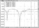
- FIG. 6 is a diagram illustrating S11 parameters of a multi band internal antenna according to the fourth embodiment of the present invention.
- FIG. 7 shows the S11 parameters of a typical inverted-F antenna.
- FIG. 8 is a diagram illustrating a structure of a multi band internal antenna according to a fourth embodiment of the present invention.
- FIG. 1 is a diagram illustrating a structure of a multi band internal antenna according to a first embodiment of the present invention.
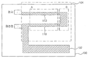
- the multi band internal antenna may include a substrate 100, a radiator 102 and an impedance matching unit 104 formed on the substrate 100.
- the substrate 100 is made of a dielectric material and other components are combined.
- Various dielectric materials may be applied to the substrate 100.
- a PCB substrate or an FR4 substrate may be used as the substrate, and the antenna carrier may serve as the substrate.
- the radiator 102 functions to radiate an RF signal of a preset frequency band to the outside and to receive an RF signal of a preset frequency band from the outside.
- the L-shaped radiating member is illustrated in FIG. 1, the shape of the radiator 102 may be applied in various forms such as a straight line shape and a meander shape.
- FIG. 1 illustrates a case in which the radiator 102 is electrically connected to the first conductive member 110, but the radiator 102 may be formed of the first conductive member 110 and the second conductive layer, as will be seen in an embodiment to be described later. It may also be electrically connected to the joining site of the member.
- the impedance matching unit 104 includes a first conductive member 110 electrically coupled with a feed point and a second conductive member 112 electrically coupled with a ground.
- the first conductive member and the second conductive member are spaced apart at predetermined intervals and are electrically connected at a specific point B.
- the impedance matching by coupling is performed at the portion A of the first conductive member 110 and the second conductive member 112 spaced apart from each other by a predetermined distance.
- the first conductive member 110 and the second conductive member 112 are electrically coupled at the B portion.
- an open stub may be formed at a portion B to which the first conductive member 110 and the second conductive member 112 are electrically coupled, and the open stub may serve as an auxiliary impedance matching. Can be.
- the structure in which coupling matching occurs in a structure in which two conductive members are spaced apart from each other by a predetermined distance enables impedance matching for a wider bandwidth.
- FIG. 1 illustrates a case in which the separation distance between the first conductive member 110 and the second conductive member 112 is the same and parallel to each other in the coupling matching portion.
- 112 may be non-parallel and may be implemented as a structure in which a part is bent to change a separation distance.
- FIG. 2 is a diagram illustrating a structure of a multi band internal antenna according to a second embodiment of the present invention.
- the multi-band internal antenna may include a substrate 200, a radiator 202 formed on the substrate, and an impedance matching unit 204.
- 204 may protrude from the first conductive member 210, the second conductive member 212, the plurality of first coupling elements 214 and the second conductive member 212 protruding from the first conductive member 210. It may comprise a plurality of second coupling elements (216).
- the shapes and roles of the radiator 202 and the substrate 200 are the same as those of the first embodiment shown in FIG. 1, and the structure of the impedance matching unit 204 is different from that of the first embodiment.
- the capacitive component among the inductive component and the capacitive component acts as the main element, When the capacitive component is secured and the capacitive component is diversified, better broadband characteristics can be satisfied.
- the impedance matching unit needs to secure a predetermined length so that sufficient coupling is performed.
- a large capacitive component when a large capacitive component is present, there is an advantage that a large capacitance value may be less affected by external factors such as a hand effect.
- the first coupling element 214 and the second coupling to enable diversification of the capacitive components and coupling by larger capacitive components and to substantially increase the electrical length of the impedance matching portion.
- Element 216 is additionally provided.
- the first coupling element 214 and the second coupling element 216 protrude from the first conductive member 210 and the second conductive member 212 in a rectangular shape and are formed in a manner crossing each other to form a comb as a whole. ) Form.
- This first coupling element 214 and the second coupling element 216 substantially close the distance between the first conductive member 210 and the second conductive member 212 to obtain a larger capacitive component. Not only can this be done, it can also contribute to the diversification of capacitive components, allowing for more broadband matching.
- first conductive member 210 and the second conductive member 212 are electrically coupled at the feature point B in the impedance matching unit according to the second embodiment.
- an open stub may be formed for more efficient impedance matching at the point where the first conductive member 210 and the second conductive member 212 are electrically coupled.
- first and second coupling elements 216 illustrates a case in which the protruding first coupling element 214 and the second coupling element 216 have a rectangular shape, but the shapes of the first and second coupling elements may be variously set. There will be.
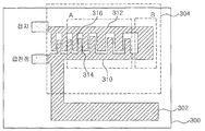
- FIG. 3 is a diagram illustrating a structure of a multi band internal antenna according to a third embodiment of the present invention.
- the multi-band internal antenna includes a substrate 300, a radiator 302, and an impedance matching unit 304, and the impedance matching unit 304 includes a feed point First conductive member 310 electrically connected, second conductive member 312 electrically connected to ground, a plurality of first coupling elements 314 and second conductive protruding from the first conductive member 310.
- a second coupling element 316 protruding from the member 312.
- the components of the impedance matching unit 304 are the same as those of the second embodiment, but the structure in which the first coupling element 314 and the second coupling element 316 are formed is different from that of the second embodiment. Do.
- the length and width of the protrusion of the first coupling element 314 and the second coupling element 316 were uniform.
- the protruding length and width of the first coupling element 314 and the second coupling element 316 are set differently.
- FIG. 3 illustrates a case in which the width and the length of the first coupling element 314 protruding from the first conductive member 310 sequentially increase, and the width and the length of the first coupling element 314 decrease about the center thereof. Is shown. In addition, in the case of the second coupling element 316 protruding from the second conductive member 312, it is shown that the protruding length is the same but the width continues to increase sequentially.
- setting the width and length of the coupling elements 314 and 316 in various ways is to maximize the diversification of the capacitive component.
- the width and length of the coupling elements may be adapted in various forms.
- width and length of the coupling elements may be changed, and the width and length may be changed at the same time.
- FIG. 8 is a diagram illustrating the structure of a multi band internal antenna according to a fourth embodiment of the present invention.
- the multi-band internal antenna includes a substrate 800, a radiator 802, and an impedance matching unit 804, and the impedance matching unit 804 includes the feed point.
- the antenna according to the fourth embodiment differs from the second embodiment only in the coupled state of the radiator 802 and the other components are the same as in the second embodiment.
- the radiator 802 extends from a coupling portion between the first conductive member 810 and the second conductive member 812. That is, the radiator 802 may extend from the first conductive member 810 and may extend from the coupling portion of the first conductive member 810 and the second conductive member 812 as described above.
- the radiator form of the fourth embodiment as shown in FIG. 8 can also be applied to the first and third embodiments.
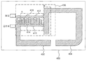
- FIG. 4 is a diagram illustrating a structure of a multi band internal antenna according to a fifth embodiment of the present invention.
- the multi-band internal antenna may include a substrate 400, a first radiator 402, a second radiator 404, and an impedance matching unit 406. .
- the fifth embodiment is provided with two radiators 402 and 404.
- Two radiators 402, 404 are provided for transmitting and receiving frequency signals of more bands.
- the first radiator 402 having a short electrical length is a radiator for radiating a high frequency band frequency signal
- the second radiator with a long electrical length is a radiator for radiating a low frequency band frequency signal.
- the first radiator 402 extends from the first conductive member 410
- the second radiator 404 extends from the coupling portion B of the first conductive member 410 and the second conductive member 412.
- the first radiator 402 can accommodate the DCS, PCS, WCDMA and Bluetooth bands and the second radiator 404 can accommodate the GSM850 and GSM950 bands.
- the impedance matching unit 406 includes a first conductive member 410 electrically connected to a feed point and a second conductive member 412 electrically connected to a ground.
- the impedance matching unit 406 includes a plurality of first coupling elements 414 protruding from the first conductive member 410 and a plurality of second coupling elements 416 protruding from the second conductive member 412. It includes.
- the first and second coupling elements 414 and 416 allow coupling by larger capacitive components, such as the coupling elements of the second and third embodiments, diversify the capacitive components and provide electrical It is a component for increasing the length.
- the impedance matching unit shown in the third embodiment is shown in FIG. 4, the impedance matching unit may be any of the impedance matching units shown in the first to third embodiments.
- FIG. 4 illustrates a case in which the second radiator has a 'c' shape bent twice, but the shape of the second radiator is not limited thereto.
- frequency signals can be transmitted and received for multiple bands while maintaining broadband characteristics in the high frequency band.
- FIG. 5 is a diagram illustrating a structure in which a multi band internal antenna according to a fifth embodiment of the present invention is coupled to a carrier.
- the carrier 500 having a '-' shape is coupled to the PCB 506 of the terminal, and the carrier 500 includes a vertical portion 502 and a flat portion 504.
- the first conductive member and the second conductive member of the impedance matching portion extend to the vertical portion 502 of the carrier so that the first conductive member is coupled with the feed line formed on the PCB, and the second conductive member is coupled with the ground formed on the PCB.
- FIG. 6 is a diagram illustrating S11 parameters of a multiband internal antenna according to a fifth embodiment of the present invention
- FIG. 7 is a diagram illustrating S11 parameters of a general inverted-F antenna.
- the antenna according to the fourth embodiment of the present invention exhibits a wide band characteristic in the high frequency band, whereas the inverted-F antenna has a narrow band characteristic in the high frequency band. Service is available.
Landscapes
- Engineering & Computer Science (AREA)
- Computer Networks & Wireless Communication (AREA)
- Details Of Aerials (AREA)
- Waveguide Aerials (AREA)
Abstract
Priority Applications (3)
| Application Number | Priority Date | Filing Date | Title |
|---|---|---|---|
| US12/935,195 US8587494B2 (en) | 2008-03-31 | 2009-03-30 | Internal antenna providing impedance matching for multiband |
| CN200980111797XA CN101981754A (zh) | 2008-03-31 | 2009-03-30 | 支持针对多频带的阻抗匹配的内置型天线 |
| EP09754902A EP2262057A4 (fr) | 2008-03-31 | 2009-03-30 | Antenne intégrée pour prendre en charge l'adaptation d'impédance pour le mode multibande |
Applications Claiming Priority (2)
| Application Number | Priority Date | Filing Date | Title |
|---|---|---|---|
| KR10-2008-0029714 | 2008-03-31 | ||
| KR1020080029714A KR100980218B1 (ko) | 2008-03-31 | 2008-03-31 | 다중 대역에 대한 임피던스 매칭을 지원하는 내장형 안테나 |
Publications (2)
| Publication Number | Publication Date |
|---|---|
| WO2009145437A2 true WO2009145437A2 (fr) | 2009-12-03 |
| WO2009145437A3 WO2009145437A3 (fr) | 2010-01-21 |
Family
ID=41377704
Family Applications (1)
| Application Number | Title | Priority Date | Filing Date |
|---|---|---|---|
| PCT/KR2009/001608 WO2009145437A2 (fr) | 2008-03-31 | 2009-03-30 | Antenne intégrée pour prendre en charge l'adaptation d'impédance pour le mode multibande |
Country Status (5)
| Country | Link |
|---|---|
| US (1) | US8587494B2 (fr) |
| EP (1) | EP2262057A4 (fr) |
| KR (1) | KR100980218B1 (fr) |
| CN (1) | CN101981754A (fr) |
| WO (1) | WO2009145437A2 (fr) |
Cited By (2)
| Publication number | Priority date | Publication date | Assignee | Title |
|---|---|---|---|---|
| US11369730B2 (en) | 2016-09-29 | 2022-06-28 | Smith & Nephew, Inc. | Construction and protection of components in negative pressure wound therapy systems |
| US11974903B2 (en) | 2017-03-07 | 2024-05-07 | Smith & Nephew, Inc. | Reduced pressure therapy systems and methods including an antenna |
Families Citing this family (14)
| Publication number | Priority date | Publication date | Assignee | Title |
|---|---|---|---|---|
| KR101120864B1 (ko) * | 2010-03-31 | 2012-03-16 | 주식회사 에이스앤파트너스 | 개선된 임피던스 매칭을 지원하는 전자기 결합을 이용한 광대역 내장형 안테나 |
| TWI450441B (zh) | 2011-02-25 | 2014-08-21 | Acer Inc | 行動通訊裝置及其天線結構 |
| KR101257093B1 (ko) * | 2011-06-10 | 2013-04-19 | 엘지전자 주식회사 | 이동 단말기 |
| KR101316153B1 (ko) * | 2011-09-28 | 2013-10-08 | 엘지이노텍 주식회사 | 안테나 |
| KR101347993B1 (ko) * | 2011-10-25 | 2014-01-08 | 주식회사 에이스테크놀로지 | 단말기 하우징에 결합되는 안테나 |
| US8723739B2 (en) * | 2012-05-11 | 2014-05-13 | Perfect Wireless (Taiwan) Technology Co., Ltd. | Multi-frequency antenna |
| KR101323134B1 (ko) | 2012-06-01 | 2013-10-30 | 주식회사 이엠따블유 | 안테나 및 이를 포함하는 통신 장치 |
| FR2996362B1 (fr) * | 2012-10-01 | 2015-09-04 | Hager Security | Dispositif d'antenne electromagnetique |
| CN104347926B (zh) * | 2013-07-31 | 2017-04-19 | 华为终端有限公司 | 一种印制天线和终端设备 |
| JP2015170961A (ja) * | 2014-03-06 | 2015-09-28 | ホシデン株式会社 | アンテナ装置、当該アンテナ装置を用いた送信モジュール、及び当該送信モジュールを用いた位置特定システム |
| US9363794B1 (en) * | 2014-12-15 | 2016-06-07 | Motorola Solutions, Inc. | Hybrid antenna for portable radio communication devices |
| CN105870618B (zh) * | 2016-05-13 | 2019-04-12 | 电子科技大学 | 一种无集总元件匹配的433MHz平面倒F天线 |
| JP7216576B2 (ja) | 2019-03-05 | 2023-02-01 | 日本航空電子工業株式会社 | アンテナ |
| JP2022178059A (ja) * | 2021-05-19 | 2022-12-02 | 日本航空電子工業株式会社 | マルチバンドアンテナ |
Family Cites Families (8)
| Publication number | Priority date | Publication date | Assignee | Title |
|---|---|---|---|---|
| CA2341743A1 (fr) * | 1999-09-30 | 2001-04-05 | Murata Manufacturing Co | Antenne montee surface et dispositif de communication le comprenant |
| JP2004104419A (ja) * | 2002-09-09 | 2004-04-02 | Hitachi Cable Ltd | 携帯無線機用アンテナ |
| US6734825B1 (en) * | 2002-10-28 | 2004-05-11 | The National University Of Singapore | Miniature built-in multiple frequency band antenna |
| JP2004172912A (ja) | 2002-11-19 | 2004-06-17 | Sony Corp | マルチバンドアンテナ |
| GB2396967A (en) * | 2002-12-30 | 2004-07-07 | Nokia Corp | Strip feed arrangement for a compact internal planar antenna element |
| JP2006197254A (ja) | 2005-01-13 | 2006-07-27 | Sakae Riken Kogyo Co Ltd | 自動車用アンテナ |
| TWI253782B (en) * | 2005-07-11 | 2006-04-21 | Wistron Neweb Corp | Antenna |
| JP2007123982A (ja) | 2005-10-25 | 2007-05-17 | Sony Ericsson Mobilecommunications Japan Inc | マルチバンド対応アンテナ装置および通信端末装置 |
-
2008
- 2008-03-31 KR KR1020080029714A patent/KR100980218B1/ko active IP Right Grant
-
2009
- 2009-03-30 CN CN200980111797XA patent/CN101981754A/zh active Pending
- 2009-03-30 EP EP09754902A patent/EP2262057A4/fr not_active Withdrawn
- 2009-03-30 WO PCT/KR2009/001608 patent/WO2009145437A2/fr active Application Filing
- 2009-03-30 US US12/935,195 patent/US8587494B2/en active Active
Non-Patent Citations (2)
| Title |
|---|
| None |
| See also references of EP2262057A4 |
Cited By (2)
| Publication number | Priority date | Publication date | Assignee | Title |
|---|---|---|---|---|
| US11369730B2 (en) | 2016-09-29 | 2022-06-28 | Smith & Nephew, Inc. | Construction and protection of components in negative pressure wound therapy systems |
| US11974903B2 (en) | 2017-03-07 | 2024-05-07 | Smith & Nephew, Inc. | Reduced pressure therapy systems and methods including an antenna |
Also Published As
| Publication number | Publication date |
|---|---|
| US20110043427A1 (en) | 2011-02-24 |
| US8587494B2 (en) | 2013-11-19 |
| EP2262057A4 (fr) | 2011-09-07 |
| CN101981754A (zh) | 2011-02-23 |
| WO2009145437A3 (fr) | 2010-01-21 |
| KR100980218B1 (ko) | 2010-09-06 |
| EP2262057A2 (fr) | 2010-12-15 |
| KR20090104333A (ko) | 2009-10-06 |
Similar Documents
| Publication | Publication Date | Title |
|---|---|---|
| WO2009145437A2 (fr) | Antenne intégrée pour prendre en charge l'adaptation d'impédance pour le mode multibande | |
| WO2009088231A2 (fr) | Antenne intérieure multibande | |
| WO2010119998A1 (fr) | Antenne large bande mettant en oeuvre l'appariement par couplage | |
| WO2009134013A2 (fr) | Antenne interne à large bande utilisant une structure à ondes lentes | |
| WO2010119999A1 (fr) | Antenne a large bande dotée d'une adaptation couplée avec l'extrémité court-circuitée d'un émetteur | |
| KR100723086B1 (ko) | 비대칭 다이폴 안테나 어셈블리 | |
| CN101512835B (zh) | 多频带天线布置 | |
| US8786499B2 (en) | Multiband antenna system and methods | |
| FI113911B (fi) | Menetelmä signaalin kytkemiseksi ja antennirakenne | |
| US20080303729A1 (en) | Multiband antenna system and methods | |
| WO2010030128A2 (fr) | Antenne multibande utilisant un couplage électromagnétique | |
| WO2011122821A2 (fr) | Antenne interne à large bande utilisant un couplage électromagnétique supportant une correspondance d'impédance améliorée | |
| WO2010038929A1 (fr) | Antenne multicouche | |
| US6292144B1 (en) | Elongate radiator conformal antenna for portable communication devices | |
| US7482984B2 (en) | Hoop antenna | |
| WO2010071265A1 (fr) | Antenne incorporée capable d'appariement d'impédance large bande et comportant une plaque couplée à un substrat | |
| KR200441931Y1 (ko) | 슬롯형 다중대역 옴니안테나 | |
| US10374311B2 (en) | Antenna for a portable communication device | |
| KR20090126001A (ko) | 휴대용 단말기 내장형 안테나 | |
| WO2010067924A1 (fr) | Antenne intérieure acceptant une adaptation d'impédance à large bande | |
| WO2010101373A2 (fr) | Antenne large bande et multibande et appareil de communication comprenant une telle antenne | |
| KR101090114B1 (ko) | 전자기 결합을 이용한 광대역 내장형 안테나 | |
| US10243269B2 (en) | Antenna | |
| KR20100099076A (ko) | 다중 대역 내장형 안테나 | |
| KR100876475B1 (ko) | 내장형 안테나 |
Legal Events
| Date | Code | Title | Description |
|---|---|---|---|
| WWE | Wipo information: entry into national phase |
Ref document number: 200980111797.X Country of ref document: CN |
|
| 121 | Ep: the epo has been informed by wipo that ep was designated in this application |
Ref document number: 09754902 Country of ref document: EP Kind code of ref document: A2 |
|
| WWE | Wipo information: entry into national phase |
Ref document number: 6158/CHENP/2010 Country of ref document: IN Ref document number: 2009754902 Country of ref document: EP |
|
| NENP | Non-entry into the national phase |
Ref country code: DE |
|
| WWE | Wipo information: entry into national phase |
Ref document number: 12935195 Country of ref document: US |