최근 이동통신 단말기는 소형화 및 경량화되면서도, 서로 다른 주파수 대역의 이동통신 서비스를 하나의 단말기를 이용하여 제공받을 수 있는 기능이 요구되고 있다. 예를 들어, 한국에서 상용화된 824~894 MHz 대역의 CDMA 서비스와, 1750~1870 MHz 대역의 PCS 서비스, 일본에서 상용화된 832~925 MHz 대역의 CDMA 서비스, 미국에서 상용화된 1850~1990 MHz 대역의 PCS 서비스, 유럽, 중국 등에 상용화된 880~960 MHz 대역의 GSM 서비스 및 유럽 일부 지역에서 상용화된 1710~1880 MHz 대역의 DCS 서비스 등의 다양한 주파수 대역을 이용한 이동통신 서비스 가운데 필요에 따라 다중 대역의 신호를 동시에 이용할 수 있는 단말기가 요구되고 있으며 이러한 다중 대역의 수용을 위해 광대역 특성을 가지는 안테나가 요구되고 있다. Recently, a mobile terminal has been required to have a small size and a light weight, and to receive a mobile communication service having a different frequency band using a single terminal. For example, CDMA services in the 824-894 MHz band commercially available in Korea, PCS services in the 1750-1870 MHz band, CDMA services in the 832-925 MHz band commercially available in Japan, and the 1850-1990 MHz band commercially available in the US. Multi-band signal as needed among mobile communication services using various frequency bands such as PCS service, GSM service of 880 ~ 960 MHz band commercialized in Europe, China, and DCS service of 1710 ~ 1880 MHz band commercialized in some parts of Europe. There is a demand for a terminal capable of simultaneously using the antenna, and an antenna having a wideband characteristic is required for accommodating such multiple bands.
이외에도 블루투스, 지그비, 무선랜, GPS 등과 같은 서비스를 이용할 수 있는 복합 단말기가 요구되고 있는 실정이다. 이와 같은 다중 대역의 서비스를 이용하기 위한 단말기에는 원하는 둘 이상의 대역에서 동작할 수 있는 다중 대역 안테나가 사용되어야 한다. 일반적으로 사용되는 이동통신 단말기의 안테나로는 헬리컬 안테나(helical antenna)와 평면 역-F 안테나(Planar Inverted F Antenna: PIFA)가 주로 사용된다.In addition, there is a demand for a composite terminal that can use services such as Bluetooth, Zigbee, WLAN, and GPS. In order to use such a multi-band service, a multi-band antenna capable of operating in two or more bands desired should be used. In general, helical antennas and Planar Inverted F Antennas (PIFAs) are mainly used as antennas of mobile communication terminals.
여기서, 헬리컬 안테나는 단말기 상단에 고정된 외장형 안테나로서 모노폴 안테나와 함께 사용된다. 헬리컬 안테나와 모노폴 안테나가 병용되는 형태는 안테나를 단말기 본체로부터 인출(extended)하면 모노폴 안테나로 동작하고, 삽입(Retracted)하면 λ/4 헬리컬 안테나로 동작한다. 이러한 안테나는 높은 이득을 얻을 수 있는 장점이 있으나, 무지향성으로 인해 전자파 인체 유해기준인 SAR 특성이 좋지 않다. 또한, 헬리컬 안테나는 단말기의 외부에 돌출된 모양으로 구성되므로, 단말기의 미적외관 및 휴대기능에 적합한 외관 설계가 어려운데, 이에 대한 내장형의 구조는 아직 연구된 바 없다. Here, the helical antenna is used together with the monopole antenna as an external antenna fixed to the top of the terminal. When the helical antenna and the monopole antenna are used together, the antenna operates as a monopole antenna when the antenna is extended from the main body of the terminal, and as a λ / 4 helical antenna when the antenna is extended. These antennas have the advantage of obtaining high gain, but due to their omni-directional, SAR characteristics, which are harmful to the human body of electromagnetic waves, are not good. In addition, since the helical antenna is configured to protrude to the outside of the terminal, it is difficult to design the exterior suitable for the aesthetics and the portable function of the terminal, but the internal structure thereof has not been studied.
그리고, 역-F 안테나는 이러한 단점을 극복하기 위하여, 낮은 프로파일 구조를 갖도록 설계된 안테나이다. 역-F 안테나는 상기 방사부에 유기된 전류에 의해 발생되는 전체 빔 중 접지면측으로 향하는 빔이 재유기되어 인체에 향하는 빔을 감쇠시켜 SAR 특성을 개선하는 동시에 방사부 방향으로 유기되는 빔을 강화시키는 지향성을 가지며, 직사각형인 평판형 방사부의 길이가 절반으로 감소된 직사각형의 마이크로 스트립 안테나로서 작동하게 되어 낮은 프로파일 구조를 실현할 수 있다.And, an inverted-F antenna is an antenna designed to have a low profile structure to overcome this disadvantage. The inverted-F antenna reinforces the beam directed toward the ground plane of the entire beams generated by the current induced in the radiator to attenuate the beam directed to the human body, thereby improving SAR characteristics and reinforcing the beam directed toward the radiator. In order to achieve a low profile structure, it is possible to operate as a rectangular microstrip antenna whose length is rectangular and the rectangular flat radiating portion is reduced by half.
이러한 역-F 안테나는 인체방향으로 빔의 세기를 감쇠시키며 인체 바깥 방향으로 빔의 세기를 강하게 해주는 지향성을 갖는 방사 특성을 가지므로 헬리컬 안테나와 비교하였을 때 전자파 흡수율이 우수한 특성을 얻을 수 있다. 그러나, 역F 안테나는 다중 대역에서 동작하도록 설계 하였을 경우 주파수 대역폭이 협소한 문제점이 있다. Such an inverted-F antenna has a radiation characteristic having a directivity that attenuates the beam strength in the human body direction and strengthens the beam strength in the human body direction, and thus, an electromagnetic wave absorption rate is excellent when compared with a helical antenna. However, when the inverted-F antenna is designed to operate in multiple bands, there is a problem in that the frequency bandwidth is narrow.
다중 대역에서의 보다 안정적인 동작을 위해 낮은 프로파일 구조를 가지면서 역F 안테나의 단점인 협대역 특성을 극복할 수 있는 안테나가 요구되고 있다. There is a need for an antenna capable of overcoming narrow band characteristics, which is a disadvantage of the inverted-F antenna, while having a low profile structure for more stable operation in multiple bands.
이하에서, 첨부된 도면을 참조하여 본 발명에 의한 다중 대역 내장형 안테나의 바람직한 실시예를 상세히 설명한다.Hereinafter, with reference to the accompanying drawings will be described in detail a preferred embodiment of the multi-band internal antenna according to the present invention.
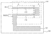
도 1은 본 발명의 제1 실시예에 따른 다중 대역 내장형 안테나의 구조를 도시한 도면이다. 1 is a diagram illustrating a structure of a multi band internal antenna according to a first embodiment of the present invention.
도 1을 참조하면, 본 발명의 제1 실시예에 따른 다중 대역 내장형 안테나는 기판(100), 기판(100)상에 형성되는 방사체(102) 및 임피던스 매칭부(104)를 포함할 수 있다. Referring to FIG. 1, the multi band internal antenna according to the first exemplary embodiment of the present invention may include a substrate 100, a radiator 102 and an impedance matching unit 104 formed on the substrate 100.
도 1에서, 기판(100)은 유전체 재질로 이루어지며 다른 구성 요소들이 결합된다. 다양한 유전체 재질이 기판(100)에 적용될 수 있다. 일례로, PCB 기판 또는 FR4 기판 등이 기판으로 사용될 수 있으며, 안테나 캐리어가 기판으로서의 역할을 수행할 수도 있다. In FIG. 1, the substrate 100 is made of a dielectric material and other components are combined. Various dielectric materials may be applied to the substrate 100. In one example, a PCB substrate or an FR4 substrate may be used as the substrate, and the antenna carrier may serve as the substrate.
방사체(102)는 미리 설정된 주파수 대역의 RF 신호를 외부에 방사하고 외부로부터 미리 설정된 주파수 대역의 RF 신호를 수신하는 기능을 한다. 도 1에는 L자 형태의 방사 부재가 도시되어 있으나 방사체102)의 형태는 직선 라인 형태, 미앤더 형태 등 다양한 형태가 적용될 수 있을 것이다. The radiator 102 functions to radiate an RF signal of a preset frequency band to the outside and to receive an RF signal of a preset frequency band from the outside. Although the L-shaped radiating member is illustrated in FIG. 1, the shape of the radiator 102 may be applied in various forms such as a straight line shape and a meander shape.
도 1에는 방사체(102)가 제1 도전 부재(110)와 전기적으로 연결되는 경우가 도시되어 있으나, 후술하는 실시예에서 확인되듯이 방사체(102)는 제1 도전 부재(110) 및 제2 도전 부재의 결합 부위와 전기적으로 연결될 수도 있다. FIG. 1 illustrates a case in which the radiator 102 is electrically connected to the first conductive member 110, but the radiator 102 may be formed of the first conductive member 110 and the second conductive layer, as will be seen in an embodiment to be described later. It may also be electrically connected to the joining site of the member.
임피던스 매칭부(104)는 급전점과 전기적으로 결합되는 제1 도전 부재(110) 및 접지와 전기적으로 결합되는 제2 도전 부재(112)를 포함한다. 제1 도전 부재 및 제2 도전 부재는 소정 간격을 두고 이격되며, 특정 지점(B)에서 전기적으로 연결된다. The impedance matching unit 104 includes a first conductive member 110 electrically coupled with a feed point and a second conductive member 112 electrically coupled with a ground. The first conductive member and the second conductive member are spaced apart at predetermined intervals and are electrically connected at a specific point B.
임피던스 매칭부(106)에서 제1 도전 부재(110) 및 제2 도전 부재(112)가 소정 거리 이격된 A 부분에서는 커플링에 의한 임피던스 매칭이 수행된다. 또한, 제1 도전 부재(110) 및 제2 도전 부재(112)는 B 부분에서 전기적으로 결합된다. In the impedance matching unit 106, the impedance matching by coupling is performed at the portion A of the first conductive member 110 and the second conductive member 112 spaced apart from each other by a predetermined distance. In addition, the first conductive member 110 and the second conductive member 112 are electrically coupled at the B portion.
도 1에는 도시되어 있지 않으나, 제1 도전 부재(110) 및 제2 도전 부재(112)가 전기적으로 결합되는 B 부분에 오픈 스터브가 형성될 수도 있으며, 오픈 스터브는 보조적인 임피던스 매칭 역할을 수행할 수 있다. Although not shown in FIG. 1, an open stub may be formed at a portion B to which the first conductive member 110 and the second conductive member 112 are electrically coupled, and the open stub may serve as an auxiliary impedance matching. Can be.
이와 같이, 두 개의 도전 부재가 소정 거리 이격된 구조에서 발생하는 커플링 매칭이 이루어지는 구조는 보다 광대역에 대한 임피던스 매칭이 가능하도록 한다.As such, the structure in which coupling matching occurs in a structure in which two conductive members are spaced apart from each other by a predetermined distance enables impedance matching for a wider bandwidth.
도 1에는 커플링 매칭 부분에서 제1 도전 부재(110) 및 제2 도전 부재(112)의 이격 거리가 동일하여 서로 평행한 경우가 도시되어 있으나, 제1 도전 부재(110) 및 제2 도전 부재(112)는 평행하지 않을 수도 있으며 일부가 절곡되어 이격 거리가 달라지는 구조로도 구현 가능하다. FIG. 1 illustrates a case in which the separation distance between the first conductive member 110 and the second conductive member 112 is the same and parallel to each other in the coupling matching portion. 112 may be non-parallel and may be implemented as a structure in which a part is bent to change a separation distance.
도 2는 본 발명의 제2 실시예에 따른 다중 대역 내장형 안테나의 구조를 도시한 도면이다. 2 is a diagram illustrating a structure of a multi band internal antenna according to a second embodiment of the present invention.
도 2를 참조하면, 본 발명의 제2 실시예에 따른 다중 대역 내장형 안테나는 기판(200), 기판상에 형성되는 방사체(202) 및 임피던스 매칭부(204)를 포함할 수 있으며, 임피던스 매칭부(204)는 제1 도전 부재(210), 제2 도전 부재(212), 제1 도전 부재(210)로부터 돌출되는 다수의 제1 커플링 엘리먼트(214) 및 제2 도전 부재(212)로부터 돌출되는 다수의 제2 커플링 엘리먼트(216)를 포함할 수 있다.Referring to FIG. 2, the multi-band internal antenna according to the second embodiment of the present invention may include a substrate 200, a radiator 202 formed on the substrate, and an impedance matching unit 204. 204 may protrude from the first conductive member 210, the second conductive member 212, the plurality of first coupling elements 214 and the second conductive member 212 protruding from the first conductive member 210. It may comprise a plurality of second coupling elements (216).
도 2를 참조하면, 방사체(202) 및 기판(200)의 형상 및 역할은 도 1에 도시된 제1 실시예와 동일하며 임피던스 매칭부(204)의 구조가 제1 실시예와 상이하다. Referring to FIG. 2, the shapes and roles of the radiator 202 and the substrate 200 are the same as those of the first embodiment shown in FIG. 1, and the structure of the impedance matching unit 204 is different from that of the first embodiment.
제1 도전 부재(210) 및 제2 도전 부재(212)의 상호 작용에 의한 커플링 매칭이 수행될 때, 유도성 성분과 용량성 성분 중 용량성 성분이 보다 주요한 요소로 작용하게 되며, 보다 큰 용량성 성분이 확보되고 용량성 성분이 다양화할 때 보다 좋은 광대역 특성을 만족시킬 수 있다. When coupling matching by the interaction of the first conductive member 210 and the second conductive member 212 is performed, the capacitive component among the inductive component and the capacitive component acts as the main element, When the capacitive component is secured and the capacitive component is diversified, better broadband characteristics can be satisfied.
또한, 광대역 매칭을 위해서는 임패던스 매칭부가 소정 길이를 확보하여 충분한 커플링이 이루어져야 할 필요가 있다. In addition, for wideband matching, the impedance matching unit needs to secure a predetermined length so that sufficient coupling is performed.
나아가, 큰 용량성 성분이 존재할 경우 큰 캐패시턴스 값으로 인해 핸드 이펙트(hand effect)와 같은 외부적인 요인에 보다 영향을 적게 받을 수 있는 장점이 있다. Furthermore, when a large capacitive component is present, there is an advantage that a large capacitance value may be less affected by external factors such as a hand effect.
도 2를 참조하면, 용량성 성분의 다양화 및 보다 큰 용량성 성분에 의한 커플링을 가능하도록 하고 임피던스 매칭부의 전기적 길이를 실질적으로 증가시키기 위해 제1 커플링 엘리먼트(214) 및 제2 커플링 엘리먼트(216)가 추가적으로 구비된다. Referring to FIG. 2, the first coupling element 214 and the second coupling to enable diversification of the capacitive components and coupling by larger capacitive components and to substantially increase the electrical length of the impedance matching portion. Element 216 is additionally provided.
제1 커플링 엘리먼트(214) 및 제2 커플링 엘리먼트(216)는 직사각형 형태로 제1 도전 부재(210) 및 제2 도전 부재(212)로부터 돌출되며 서로 교차하는 방식으로 형성되어 전체적으로 빗살(Comb) 형태를 이룬다. The first coupling element 214 and the second coupling element 216 protrude from the first conductive member 210 and the second conductive member 212 in a rectangular shape and are formed in a manner crossing each other to form a comb as a whole. ) Form.
이와 같은 제1 커플링 엘리먼트(214) 및 제2 커플링 엘리먼트(216)는 제1 도전 부재(210)와 제2 도전 부재(212) 사이의 거리를 실질적으로 가깝게 하여 보다 큰 용량성 성분의 획득이 가능하도록 할 뿐만 아니라 용량성 성분의 다양화에도 기여할 수 있어 보다 광대역에 대한 매칭이 가능하도록 한다. This first coupling element 214 and the second coupling element 216 substantially close the distance between the first conductive member 210 and the second conductive member 212 to obtain a larger capacitive component. Not only can this be done, it can also contribute to the diversification of capacitive components, allowing for more broadband matching.
한편, 제2 실시예에 따른 임피던스 매칭부에서도 특징 지점 B 에서 제1 도전 부재(210) 및 제2 도전 부재(212)가 전기적으로 결합된다. 아울러, 도 2에는 도시되어 있지 않으나 제1 도전 부재(210) 및 제2 도전 부재(212) 전기적으로 결합되는 지점에서 보다 효율적인 임피던스 매칭을 위한 오픈 스터브가 형성될 수도 있다. Meanwhile, the first conductive member 210 and the second conductive member 212 are electrically coupled at the feature point B in the impedance matching unit according to the second embodiment. In addition, although not shown in FIG. 2, an open stub may be formed for more efficient impedance matching at the point where the first conductive member 210 and the second conductive member 212 are electrically coupled.
도 2에는 돌출되는 제1 커플링 엘리먼트(214) 및 제2 커플링 엘리먼트(216)의 형상이 장방형의 직사각형인 경우가 도시되어 있으나 제1 및 제2 커플링 엘리먼트의 형상은 다양하게 설정될 수 있을 것이다. 2 illustrates a case in which the protruding first coupling element 214 and the second coupling element 216 have a rectangular shape, but the shapes of the first and second coupling elements may be variously set. There will be.
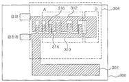
도 3은 본 발명의 제3 실시예에 따른 다중 대역 내장형 안테나의 구조를 도시한 도면이다. 3 is a diagram illustrating a structure of a multi band internal antenna according to a third embodiment of the present invention.
도 3을 참조하면, 본 발명의 제3 실시예에 따른 다중 대역 내장형 안테나는 기판(300), 방사체(302) 및 임피던스 매칭부(304)를 포함하며, 임피던스 매칭부(304)는 급전점과 전기적으로 연결되는 제1 도전 부재(310) 및 접지와 전기적으로 연결되는 제2 도전 부재(312), 제1 도전 부재(310)로부터 돌출되는 다수의 제1 커플링 엘리먼트(314) 및 제2 도전 부재(312)로부터 돌출되는 제2 커플링 엘리먼트(316)를 포함한다. Referring to FIG. 3, the multi-band internal antenna according to the third embodiment of the present invention includes a substrate 300, a radiator 302, and an impedance matching unit 304, and the impedance matching unit 304 includes a feed point First conductive member 310 electrically connected, second conductive member 312 electrically connected to ground, a plurality of first coupling elements 314 and second conductive protruding from the first conductive member 310. A second coupling element 316 protruding from the member 312.
제3 실시예의 안테나는 임피던스 매칭부(304)의 구성 요소는 제2 실시예와 동일하나 제1 커플링 엘리먼트(314) 및 제2 커플링 엘리먼트(316)가 형성된 구조가 제2 실시예와 상이하다. In the antenna of the third embodiment, the components of the impedance matching unit 304 are the same as those of the second embodiment, but the structure in which the first coupling element 314 and the second coupling element 316 are formed is different from that of the second embodiment. Do.
제2 실시예에서, 제1 커플링 엘리먼트(314) 및 제2 커플링 엘리먼트(316)가 돌출된 길이 및 폭은 균일하였다. 그러나, 도 3에 도시된 바와 같이 본 발명의 제3 실시예에 따르면 제1 커플링 엘리먼트(314)와 제2 커플링 엘리먼트(316)의 돌출 길이 및 폭은 상이하게 설정된다. In the second embodiment, the length and width of the protrusion of the first coupling element 314 and the second coupling element 316 were uniform. However, as shown in FIG. 3, according to the third embodiment of the present invention, the protruding length and width of the first coupling element 314 and the second coupling element 316 are set differently.
도 3에는 제1 도전 부재(310)로부터 돌출되는 제1 커플링 엘리먼트(314)의 폭 및 길이가 순차적으로 증가하다가 중앙을 중심으로 제1 커플링 엘리먼트(314)의 폭 및 길이가 감소하는 경우가 도시되어 있다. 또한, 제2 도전 부재(312)로부터 돌출되는 제2 커플링 엘리먼트(316)의 경우, 돌출 길이는 동일하되 폭이 순차적으로 계속 증가하는 경우가 도시되어 있다. 3 illustrates a case in which the width and the length of the first coupling element 314 protruding from the first conductive member 310 sequentially increase, and the width and the length of the first coupling element 314 decrease about the center thereof. Is shown. In addition, in the case of the second coupling element 316 protruding from the second conductive member 312, it is shown that the protruding length is the same but the width continues to increase sequentially.
제3 실시예에서 커플링 엘리먼트들(314, 316)의 폭 및 길이를 다양하게 설정하는 것은 용량성 성분의 다양화를 보다 극대화하기 위함이다. 커플링 엘리먼트들의 폭 및 길이는 다양한 형식으로 변형되어 적용될 수 있을 것이다. In the third embodiment, setting the width and length of the coupling elements 314 and 316 in various ways is to maximize the diversification of the capacitive component. The width and length of the coupling elements may be adapted in various forms.
예를 들어, 커플링 엘리먼트들의 폭 및 길이 중 어느 하나만이 변경될 수도 있으며, 폭 및 길이가 동시에 변경될 수도 있을 것이다. For example, only one of the width and length of the coupling elements may be changed, and the width and length may be changed at the same time.
도 8은 본 발명의 제4 실시예에 따른 다중 대역 내장형 안테나의 구조를 도시한 도면이다. 8 is a diagram illustrating the structure of a multi band internal antenna according to a fourth embodiment of the present invention.
도 8을 참조하면, 본 발명의 제4 실시예에 따른 다중 대역 내장형 안테나는 기판(800), 방사체(802) 및 임피던스 매칭부(804)를 포함하며, 임피던스 매칭부(804)는 상기 급전점과 전기적으로 연결되는 제1 도전 부재(810) 및 접지와 전기적으로 연결되는 제2 도전 부재(812), 제1 도전 부재(810)로부터 돌출되는 다수의 제1 커플링 엘리먼트(814) 및 제2 도전 부재(812)로부터 돌출되는 제2 커플링 엘리먼트(816)를 포함할 수 있다. Referring to FIG. 8, the multi-band internal antenna according to the fourth embodiment of the present invention includes a substrate 800, a radiator 802, and an impedance matching unit 804, and the impedance matching unit 804 includes the feed point. A first conductive member 810 electrically connected to the first conductive member 810 and a second conductive member 812 electrically connected to the ground, a plurality of first coupling elements 814 and second protruding from the first conductive member 810. It may include a second coupling element 816 protruding from the conductive member 812.
제 4 실시예에 따른 안테나는 방사체(802)의 결합 상태만 제2 실시예와 상이하고 다른 구성 요소들은 제2 실시예와 동일하다. 도 8을 참조하면, 제4 실시예에 따른 안테나에서 방사체(802)는 제1 도전 부재(810) 및 제2 도전 부재(812)와의 결합 부위로부터 연장된다. 즉, 방사체(802)는 상술한 실시예들과 같이 제1 도전 부재(810)로부터 연장될 수도 있으며, 제1 도전 부재(810) 및 제2 도전 부재(812)의 결합 부위로부터 연장될 수도 있다. 도 8과 같은 제4 실시예의 방사체 형태는 제1 실시예 및 제3 실시에에도 적용될 수 있다. The antenna according to the fourth embodiment differs from the second embodiment only in the coupled state of the radiator 802 and the other components are the same as in the second embodiment. Referring to FIG. 8, in the antenna according to the fourth embodiment, the radiator 802 extends from a coupling portion between the first conductive member 810 and the second conductive member 812. That is, the radiator 802 may extend from the first conductive member 810 and may extend from the coupling portion of the first conductive member 810 and the second conductive member 812 as described above. . The radiator form of the fourth embodiment as shown in FIG. 8 can also be applied to the first and third embodiments.
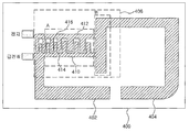
도 4는 본 발명의 제5 실시예에 따른 다중 대역 내장형 안테나의 구조를 도시한 도면이다. 4 is a diagram illustrating a structure of a multi band internal antenna according to a fifth embodiment of the present invention.
도 4를 참조하면, 본 발명의 제5 실시예에 따른 다중 대역 내장형 안테나는 기판(400), 제1 방사체(402), 제2 방사체(404) 및 임피던스 매칭부(406)를 포함할 수 있다. Referring to FIG. 4, the multi-band internal antenna according to the fifth embodiment of the present invention may include a substrate 400, a first radiator 402, a second radiator 404, and an impedance matching unit 406. .
제1 내지 제4 실시예와 비교할 때, 제5 실시예에는 두 개의 방사체(402, 404)가 구비된다. 두 개의 방사체(402, 404)는 보다 많은 대역의 주파수 신호를 송수신하기 위해 구비된다. 도 4에서, 전기적 길이가 짧은 제1 방사체(402)는 고주파 대역의 주파수 신호를 방사하기 위한 방사체이며, 전기적 길이가 긴 제2 방사체(404)는 저주파 대역의 주파수 신호를 방사하기 위한 방사체이다. 제1 방사체(402)는 제1 도전 부재(410)로부터 연장되며, 제2 방사체(404)는 제1 도전 부재(410) 및 제2 도전 부재(412)의 결합 부위(B)로부터 연장된다. Compared with the first to fourth embodiments, the fifth embodiment is provided with two radiators 402 and 404. Two radiators 402, 404 are provided for transmitting and receiving frequency signals of more bands. In FIG. 4, the first radiator 402 having a short electrical length is a radiator for radiating a high frequency band frequency signal, and the second radiator with a long electrical length is a radiator for radiating a low frequency band frequency signal. The first radiator 402 extends from the first conductive member 410, and the second radiator 404 extends from the coupling portion B of the first conductive member 410 and the second conductive member 412.
본 발명의 일 실시예에 따르면, 제1 방사체(402)는 DCS, PCS, WCDMA 및 블루투스 대역을 수용하고 제2 방사체(404)는 GSM850 및 GSM950 대역을 수용할 수 있다. According to one embodiment of the invention, the first radiator 402 can accommodate the DCS, PCS, WCDMA and Bluetooth bands and the second radiator 404 can accommodate the GSM850 and GSM950 bands.
임피던스 매칭부(406)는 급전점과 전기적으로 연결되는 제1 도전 부재(410) 및 접지와 전기적으로 연결되는 제2 도전 부재(412)를 포함한다. The impedance matching unit 406 includes a first conductive member 410 electrically connected to a feed point and a second conductive member 412 electrically connected to a ground.
또한, 임피던스 매칭부(406)는 제1 도전 부재(410)로부터 돌출되는 다수의 제1 커플링 엘리먼트(414) 및 제2 도전 부재(412)로부터 돌출되는 다수의 제2 커플링 엘리먼트(416)를 포함한다. 제1 및 제2 커플링 엘리먼트(414, 416)는 제2 및 제3 실시예의 커플링 엘리먼트와 같이 보다 큰 용량성 성분에 의한 커플링을 가능하게 하고 용량성 성분의 다양화하며 임피던스 매칭부의 전기적 길이를 증가시키기 위한 구성 요소이다. In addition, the impedance matching unit 406 includes a plurality of first coupling elements 414 protruding from the first conductive member 410 and a plurality of second coupling elements 416 protruding from the second conductive member 412. It includes. The first and second coupling elements 414 and 416 allow coupling by larger capacitive components, such as the coupling elements of the second and third embodiments, diversify the capacitive components and provide electrical It is a component for increasing the length.
한편, 도 4에는 제3 실시예에 도시된 임피던스 매칭부가 도시되어 있으나 임피던스 매칭부는 제1 내지 제3 실시예에 도시된 임피던스 매칭부 중 어느 것을 적용하여도 무방하다. Meanwhile, although the impedance matching unit shown in the third embodiment is shown in FIG. 4, the impedance matching unit may be any of the impedance matching units shown in the first to third embodiments.
또한, 도 4에는 제2 방사체가 2번에 걸쳐 절곡된 'ㄷ'자 형태인 경우가 도시되어 있으나 제2 방사체의 형태가 이에 한정되는 것은 아니다. In addition, FIG. 4 illustrates a case in which the second radiator has a 'c' shape bent twice, but the shape of the second radiator is not limited thereto.
도 4와 같이 둘 이상의 방사 부재가 사용될 경우 고주파 대역에서의 광대역 특성을 유지하면서 다중 대역에 대한 주파수 신호 송수신이 가능하다. When two or more radiating members are used as shown in FIG. 4, frequency signals can be transmitted and received for multiple bands while maintaining broadband characteristics in the high frequency band.
도 5는 본 발명의 제5 실시예에 따른 다중 대역 내장형 안테나가 캐리어에 결합된 구조를 도시한 도면이다. 5 is a diagram illustrating a structure in which a multi band internal antenna according to a fifth embodiment of the present invention is coupled to a carrier.
도 5를 참조하면, 단말기의 PCB(506)에 'ㄱ'자 형태의 캐리어(500)가 결합되며, 캐리어(500)는 수직부(502) 및 평면부(504)를 포함한다. 임피던스 매칭부의 제1 도전 부재 및 제2 도전 부재는 캐리어의 수직부(502)에 연장되어 제1 도전 부재는 PCB에 형성된 급전 라인과 결합되며, 제2 도전 부재는 PCB에 형성된 접지와 결합된다. Referring to FIG. 5, the carrier 500 having a '-' shape is coupled to the PCB 506 of the terminal, and the carrier 500 includes a vertical portion 502 and a flat portion 504. The first conductive member and the second conductive member of the impedance matching portion extend to the vertical portion 502 of the carrier so that the first conductive member is coupled with the feed line formed on the PCB, and the second conductive member is coupled with the ground formed on the PCB.
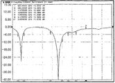
도 6은 본 발명의 제5 실시예에 따른 다중 대역 내장형 안테나의 S11 파라미터를 도시한 도면이고, 도 7은 일반적인 역-F 안테나의 S11 파라미터를 도시한 도면이다. FIG. 6 is a diagram illustrating S11 parameters of a multiband internal antenna according to a fifth embodiment of the present invention, and FIG. 7 is a diagram illustrating S11 parameters of a general inverted-F antenna.
도 6 및 도 7을 참조하면, 고주파수 대역에서는 역-F 안테나가 협소한 대역 특성을 보이는 것에 비해 본 발명의 제4 실시예에 따른 안테나는 고주파수 대역에서 광대역 특성을 보이며 이로 인해 보다 많은 대역에 대한 서비스가 가능하다.6 and 7, the antenna according to the fourth embodiment of the present invention exhibits a wide band characteristic in the high frequency band, whereas the inverted-F antenna has a narrow band characteristic in the high frequency band. Service is available.