WO2009142124A1 - 光学素子、及びそれを用いた電子機器の製造方法 - Google Patents
光学素子、及びそれを用いた電子機器の製造方法 Download PDFInfo
- Publication number
- WO2009142124A1 WO2009142124A1 PCT/JP2009/058823 JP2009058823W WO2009142124A1 WO 2009142124 A1 WO2009142124 A1 WO 2009142124A1 JP 2009058823 W JP2009058823 W JP 2009058823W WO 2009142124 A1 WO2009142124 A1 WO 2009142124A1
- Authority
- WO
- WIPO (PCT)
- Prior art keywords
- optical element
- fine particles
- inorganic fine
- substrate
- oxide
- Prior art date
- Legal status (The legal status is an assumption and is not a legal conclusion. Google has not performed a legal analysis and makes no representation as to the accuracy of the status listed.)
- Ceased
Links
Images


Classifications
-
- G—PHYSICS
- G02—OPTICS
- G02B—OPTICAL ELEMENTS, SYSTEMS OR APPARATUS
- G02B13/00—Optical objectives specially designed for the purposes specified below
- G02B13/001—Miniaturised objectives for electronic devices, e.g. portable telephones, webcams, PDAs, small digital cameras
- G02B13/0085—Miniaturised objectives for electronic devices, e.g. portable telephones, webcams, PDAs, small digital cameras employing wafer level optics
-
- H—ELECTRICITY
- H10—SEMICONDUCTOR DEVICES; ELECTRIC SOLID-STATE DEVICES NOT OTHERWISE PROVIDED FOR
- H10F—INORGANIC SEMICONDUCTOR DEVICES SENSITIVE TO INFRARED RADIATION, LIGHT, ELECTROMAGNETIC RADIATION OF SHORTER WAVELENGTH OR CORPUSCULAR RADIATION
- H10F39/00—Integrated devices, or assemblies of multiple devices, comprising at least one element covered by group H10F30/00, e.g. radiation detectors comprising photodiode arrays
- H10F39/80—Constructional details of image sensors
- H10F39/804—Containers or encapsulations
-
- Y—GENERAL TAGGING OF NEW TECHNOLOGICAL DEVELOPMENTS; GENERAL TAGGING OF CROSS-SECTIONAL TECHNOLOGIES SPANNING OVER SEVERAL SECTIONS OF THE IPC; TECHNICAL SUBJECTS COVERED BY FORMER USPC CROSS-REFERENCE ART COLLECTIONS [XRACs] AND DIGESTS
- Y10—TECHNICAL SUBJECTS COVERED BY FORMER USPC
- Y10T—TECHNICAL SUBJECTS COVERED BY FORMER US CLASSIFICATION
- Y10T29/00—Metal working
- Y10T29/49—Method of mechanical manufacture
- Y10T29/49002—Electrical device making
-
- Y—GENERAL TAGGING OF NEW TECHNOLOGICAL DEVELOPMENTS; GENERAL TAGGING OF CROSS-SECTIONAL TECHNOLOGIES SPANNING OVER SEVERAL SECTIONS OF THE IPC; TECHNICAL SUBJECTS COVERED BY FORMER USPC CROSS-REFERENCE ART COLLECTIONS [XRACs] AND DIGESTS
- Y10—TECHNICAL SUBJECTS COVERED BY FORMER USPC
- Y10T—TECHNICAL SUBJECTS COVERED BY FORMER US CLASSIFICATION
- Y10T428/00—Stock material or miscellaneous articles
- Y10T428/24—Structurally defined web or sheet [e.g., overall dimension, etc.]
- Y10T428/24355—Continuous and nonuniform or irregular surface on layer or component [e.g., roofing, etc.]
- Y10T428/24372—Particulate matter
Definitions
- the present invention relates to an optical element and a method for manufacturing an electronic device using the optical element.
- inorganic glass materials are generally used as optical elements (mainly lenses).
- optical elements mainly lenses
- miniaturization of optical elements is also required, and it has become difficult to produce an inorganic glass material having a large curvature (R) or a complicated shape due to workability problems.
- inorganic glass materials have a higher specific gravity than plastic materials, so when used as an optical element, the optical system's mass increases, and when the optical element needs to be driven, the drive voltage is set high. Therefore, there is a problem that the apparatus becomes large and power consumption increases.
- plastic materials that are easy to process and have a low specific gravity have been studied and used.
- the plastic material for the optical element include thermoplastic resins having good transparency such as polyolefin, polymethyl methacrylate, polycarbonate, and polystyrene. Further, when molding a plastic material, the lifetime of the mold is very long compared to an inorganic glass material, so that the manufacturing cost can be greatly reduced.
- solder reflow processing is performed as an optical module integrated with an optical element in a state in which an optical element is further mounted on a circuit board in addition to an electronic component, thereby producing an imaging device production system. Therefore, further improvement in production efficiency is desired.
- thermoplastic resins that have been used as conventional resin materials for optical elements are soft and melt at a relatively low temperature, so that the workability is good, but the molded optical elements are easily deformed by heat.
- the optical element itself is also exposed to heating conditions of about 260 ° C., but the optical element made of a thermoplastic resin having low heat resistance Then, shape deterioration is caused, which becomes a problem.
- the curable resin is a resin material that is liquid or exhibits fluidity before being cured, and is cured by heating or light energy such as ultraviolet light, and has good processability like a thermoplastic resin. And since it is hard to melt
- Patent Document 4 For the purpose of improving high-temperature and high-humidity resistance of inorganic compound films, a method of coating the surface of an inorganic compound with a polymerizable compound containing metal oxide fine particles as a base is known (see Patent Document 4). This technique is intended to suppress the generation of cracks due to repeated temperature changes during use, and is not intended to improve the breakage of the functional layer under higher temperature conditions such as a reflow process.
- an optical element (see Patent Document 5) having a thin film including a layer made of an organic material on the surface of a base material and having an outermost surface roughness of 20 nm or less is known.
- the purpose is to smooth the surface of the optical element with the thin film that is included, and it is not intended to be a functional layer mainly composed of an inorganic component applicable to the reflow treatment step.
- the present invention has been made in view of the above problems, and an object of the present invention is an optical element having a functional layer containing an inorganic component as a main component on the surface, and the functional layer on the surface is subjected to a reflow treatment step.
- An object of the present invention is to provide an optical element that does not break or deform even after passing. It is another object of the present invention to provide an electronic device manufacturing method in which an imaging device having an optical element of the present invention is mounted on a substrate together with electronic components and mounted by a reflow process.
- An optical element having a functional layer containing an inorganic component as a main component on the surface of a substrate containing a curable resin and inorganic fine particles, wherein at least one inorganic fine particle is present on the surface of the substrate, An optical element having a thickness of 3 nm to 100 nm.
- optical element according to any one of items 1 to 3, wherein the optical element is used in an imaging device that is mounted on a substrate together with an electronic component by reflow processing.
- the present invention at least one kind of inorganic fine particles is present on the surface of the base material containing the curable resin and the inorganic fine particles so that the surface roughness is 3 nm or more and 100 nm or less, whereby the inorganic component is a main component.
- the adhesion between the functional layer and the base material is improved, and deterioration of the functional layer such as breakage and deformation is suppressed even when exposed to heating conditions of about 260 ° C. as in the reflow process.
- the This is because the inorganic fine particles protruding moderately on the surface of the base material improve adhesion by interaction with the inorganic component of the functional layer and suppress expansion and contraction due to heat on the surface of the base material. It is considered a thing.
- the surprising effect that coloring by heating of curable resin is also suppressed is also seen.
- an optical element having a suitable refractive index and transparency can be provided without deterioration of the functional layer on the surface when mounted on the substrate from the reflow treatment step.
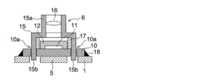
- FIG. 1 is an enlarged schematic cross-sectional view of a part of an imaging apparatus used in a preferred embodiment of the present invention. It is drawing for demonstrating schematically the manufacturing method of the imaging device in preferable embodiment of this invention.
- an imaging apparatus 100 as an electronic module has a circuit board 1 on which electronic components constituting an electronic circuit of a mobile information terminal device such as a mobile phone are mounted.
- Module 2 is mounted.
- the imaging module 2 is a small board mounting camera in which a CCD image sensor and a lens are combined.
- the imaging provided in the cover case 3 is performed.
- the image to be imaged can be captured through the opening 4 for use.
- FIG. 1 illustration of electronic components other than the electronic components of the imaging module 2 is omitted.
- the imaging module 2 includes a board module 5 and a lens module 6.
- the substrate module 5 is a light receiving module in which a CCD image sensor 11, which is an electronic component for imaging, is mounted on a sub-substrate 10, and the upper surface of the CCD image sensor 11 is sealed with a resin 12.
- a light receiving portion (not shown) in which a large number of pixels that perform photoelectric conversion are arranged in a grid pattern is formed, and an optical image is formed on the light receiving portion to store each pixel.
- the charged charges are output as an image signal.
- the sub-board 10 is mounted on the circuit board 1 by the conductive material 18, thereby fixing the sub-board 10 to the circuit board 1, and connecting electrodes (not shown) of the sub-board 10 and circuit electrodes on the upper surface of the circuit board 1. (Not shown) is electrically connected.
- the lens module 6 includes a lens case 15 that supports the lens 16.
- a lens 16 is held at the upper part of the lens case 15, and the upper part of the lens case 15 is a holder portion 15 a that holds the lens 16.
- a lower portion of the lens case 15 is inserted into a mounting hole 10 a provided in the sub-board 10 and serves as a mounting portion 15 b that fixes the lens module 6 to the sub-board 10.
- a method of pressing and fixing the mounting portion 15b into the mounting hole 10a, a method of bonding with an adhesive, or the like is used.
- the optical element of the present invention for reflow treatment can be preferably used.
- optical element of the present invention will be described in more detail.
- the present invention is characterized in that at least one kind of inorganic fine particles is present on the surface of a substrate containing a curable resin and inorganic fine particles so that the surface roughness is 3 nm or more and 100 nm or less.
- the surface roughness mentioned here is an arithmetic average roughness (Ra, JIS B0601: 2001) per 1 ⁇ m of the outermost surface of the substrate, and is more preferably 5 nm or more and 50 nm or less.
- a contact method of a stylus, an optical method using a laser, or a measurement method using an atomic force such as an atomic force microscope can be applied.
- An atomic force microscope is a particularly preferable measurement method because it can accurately measure the surface roughness.
- the region of the base material for which the arithmetic average roughness is measured is a region that is expected to be a flat portion of m of the outermost surface of the base material.
- the arithmetic average roughness per 1 ⁇ m of the surface is an average value of the entire portion.
- the region includes defects such as scratches that occur on the surface of the base material by chance in the molding process, but the surface roughness of the unevenness intentionally provided on the base material is outside the scope of the present invention.
- artificial unevenness may be provided on the surface like a diffraction pattern essential for optical function.
- the arithmetic average roughness in the region excluding this diffraction pattern is measured.
- the Ra measurement method is applied after correcting the curvature.
- variation in Ra it is required that Ra of the location of at least 4/5 or more of the number of measurement locations is 3 nm or more and 100 nm or less.
- the curable resin used in the present invention can be cured by either ultraviolet or electron beam irradiation or heat treatment, and after being mixed with inorganic fine particles in an uncured state, it is transparent by curing.
- Any resin composition can be used without particular limitation, and examples thereof include epoxy resins, vinyl ester resins, silicone resins, acrylic resins, and allyl ester resins.
- the curable resin may be an actinic ray curable resin that is cured by being irradiated with ultraviolet rays or electron beams, or may be a thermosetting resin that is cured by heat treatment. Such types of resins can be preferably used.
- silicone resin A silicone resin having a siloxane bond with Si—O—Si as the main chain can be used.
- a silicone resin made of a predetermined amount of polyorganosiloxane resin can be used (see, for example, JP-A-6-9937).
- thermosetting polyorganosiloxane resin is not particularly limited as long as it becomes a three-dimensional network structure with a siloxane bond skeleton by a continuous hydrolysis-dehydration condensation reaction by heating. It exhibits curability and has the property of being hard to be re-softened by overheating once cured.
- Such a polyorganosiloxane resin includes the following general formula (A) as a structural unit, and the shape thereof may be any of a chain, a ring, and a network.
- R1 and R2 represent the same or different substituted or unsubstituted monovalent hydrocarbon groups.
- an alkyl group such as a methyl group, an ethyl group, a propyl group, and a butyl group
- an alkenyl group such as a vinyl group and an allyl group
- an aryl group such as a phenyl group and a tolyl group
- a cycloalkyl group such as a cyclohexyl group or a cyclooctyl group, or a group in which a hydrogen atom bonded to a carbon atom of these groups is substituted with a halogen atom, a cyano group, an amino group, or the like, such as a chloromethyl group, 3, 3, 3- Examples thereof include a trifluoropropyl group, a cyanomethyl
- the polyorganosiloxane resin is usually used after being dissolved in a hydrocarbon solvent such as toluene, xylene or petroleum solvent, or a mixture of these with a polar solvent. Moreover, you may mix
- a hydrocarbon solvent such as toluene, xylene or petroleum solvent
- the method for producing the polyorganosiloxane resin is not particularly limited, and any known method can be used. For example, it can be obtained by hydrolysis or alcoholysis of one or a mixture of two or more organohalogenosilanes.
- Polyorganosiloxane resins generally contain hydrolyzable groups such as silanol groups or alkoxy groups. The group is contained in an amount of 1 to 10% by mass in terms of a silanol group.
- These reactions are generally performed in the presence of a solvent capable of melting organohalogenosilane. It can also be obtained by a method of synthesizing a block copolymer by cohydrolyzing a linear polyorganosiloxane having a hydroxyl group, an alkoxy group or a halogen atom at the molecular chain terminal with an organotrichlorosilane.
- the polyorganosiloxane resin thus obtained generally contains the remaining HCl, but in the composition of the present embodiment, the storage stability is good, so that the one having 10 ppm or less, preferably 1 ppm or less is used. Is good.
- epoxy resin examples include novolak phenol type epoxy resin, biphenyl type epoxy resin, dicyclopentadiene type epoxy resin, bisphenol F diglycidyl ether, bisphenol A diglycidyl ether, and 2,2′-bis (4-glycidyloxycyclohexyl).
- an acid anhydride curing agent As the curing agent, an acid anhydride curing agent, a phenol curing agent, or the like can be preferably used.
- acid anhydride curing agents include phthalic anhydride, maleic anhydride, trimellitic anhydride, pyromellitic anhydride, hexahydrophthalic anhydride, 3-methyl-hexahydrophthalic anhydride, 4-methyl-hexahydrophthalic anhydride
- examples thereof include an acid, a mixture of 3-methyl-hexahydrophthalic anhydride and 4-methyl-hexahydrophthalic anhydride, tetrahydrophthalic anhydride, nadic anhydride, and methyl nadic anhydride.
- a hardening accelerator is contained as needed.
- the curing accelerator is not particularly limited as long as it has good curability, is not colored, and does not impair the transparency of the thermosetting resin.
- 2-ethyl-4-methylimidazole is not limited. Imidazoles such as (2E4MZ), tertiary amines, quaternary ammonium salts, bicyclic amidines such as diazabicycloundecene and their derivatives, phosphines, phosphonium salts, etc. can be used, Two or more kinds may be mixed and used.
- inorganic fine particles examples include oxide fine particles, metal salt fine particles, and semiconductor fine particles.
- oxide fine particles are preferably used. Among these, those that do not cause absorption, light emission, fluorescence, etc. in the wavelength region used as an optical element can be appropriately selected and used.
- the metal constituting the metal oxide is Li, Na, Mg, Al, Si, K, Ca, Sc, Ti, V, Cr, Mn, Fe, Co, Ni. Cu, Zn, Rb, Sr, Y, Nb, Zr, Mo, Ag, Cd, In, Sn, Sb, Cs, Ba, La, Ta, Hf, W, Ir, Tl, Pb, Bi and rare earth metals
- a metal oxide which is one or two or more metals selected from the group can be used.
- rare earth oxides can also be used as oxide fine particles used in the present invention, specifically, scandium oxide, yttrium oxide, lanthanum oxide, cerium oxide, praseodymium oxide, neodymium oxide, samarium oxide, europium oxide, gadolinium oxide. Terbium oxide, dysprosium oxide, holmium oxide, erbium oxide, thulium oxide, ytterbium oxide, lutetium oxide and the like.
- the metal salt fine particles include carbonates, phosphates, sulfates, and the like, specifically, calcium carbonate, aluminum phosphate, and the like.
- the optical element of the present invention preferably has a light transmittance of 70% or more per optical path length of 3 mm at a wavelength of 588 nm for practical use.
- the difference in refractive index between the curable resin and the inorganic fine particles is preferably 0.07 or less in absolute value, more preferably 0.03 or less, and still more preferably 0.01 or less.
- composite oxide fine particles in which two or more kinds of metal oxides that can be adjusted to any refractive index according to the refractive index of the curable resin to be used are particularly preferably used. More preferably, composite oxide fine particles in which a metal oxide and one or more metal oxides other than silicon are combined are used.
- one kind of inorganic fine particles may be used, or a plurality of kinds of inorganic fine particles may be used in combination.
- the required characteristics can be improved more efficiently.
- the inorganic fine particles according to the present invention have an average primary particle size of 1 nm to 30 nm, preferably 1 nm to 20 nm, and more preferably 1 nm to 10 nm.
- the average primary particle size is preferably 1 nm or more, and the average primary particle size is If it exceeds 30 nm, the resulting curable resin composition may become turbid, resulting in a decrease in transparency and the light transmittance may be less than 70%. Therefore, the average primary particle size is preferably 30 nm or less.
- the average primary particle diameter here refers to the volume average value of the diameter (sphere equivalent particle diameter) when each primary particle is converted to a sphere having the same volume.
- the shape of the inorganic fine particles is not particularly limited, but spherical fine particles are preferably used.
- the minimum diameter of the particle minimum value of the distance between the tangents when drawing two tangents in contact with the outer periphery of the fine particle
- maximum diameter the value in drawing two tangents in contact with the outer periphery of the fine particle
- the maximum value of the distance between tangents is preferably 0.5 to 1.0, and more preferably 0.7 to 1.0.
- the particle size distribution is not particularly limited, but in order to achieve the effect of the present invention more efficiently, a particle having a relatively narrow distribution is preferably used rather than a particle having a wide distribution. Used.
- the inorganic fine particles of the present invention are preferably inorganic fine particles obtained by subjecting the surface of the inorganic fine particles to surface treatment, and examples of the surface treatment method of the inorganic fine particles include surface treatment with a surface modifier such as a coupling agent.
- the inorganic fine particles are treated in a solution in which the surface modifier is dissolved, and the inorganic fine particle powder is stirred in a high-speed stirring mixer such as a Hensel mixer or V-type mixer, and the surface modifier is added there. And a dry method in which the solution is dropped and reacted.
- Examples of the surface modifier used for the surface treatment of the inorganic fine particles include silane coupling agents, silicone oil-based, titanate-based, aluminate-based and zirconate-based coupling agents, but are not particularly limited.
- a silane coupling agent is preferably used.
- silane coupling agent examples include vinylsilazane trimethylchlorosilane, dimethyldichlorosilane, methyltrichlorosilane, trimethylalkoxysilane, dimethyldialkoxysilane, methyltrialkoxysilane, and hexamethyldisilazane. In order to cover widely, hexamethyldisilazane or the like is preferably used.
- the ratio of the surface modification is not particularly limited, but the ratio of the surface modifier is preferably in the range of 10 to 99% by mass with respect to the inorganic fine particles after the surface modification, and is preferably 30 to 98% by mass. A range is more preferable.
- the present invention is a substrate containing the curable resin and the inorganic fine particles, and the inorganic fine particles are present on the surface of the substrate.
- the surface of a base material here means the range from the outermost surface of a base material to the depth of 1 micrometer, and the surface roughness of this base material is 3 nm or more and 100 nm or less because this inorganic fine particle exists in this. It is characterized by becoming. Moreover, it is more preferable that the inorganic fine particles protrude from the surface of the substrate.
- the “protrusion” in the present invention refers to a state in which inorganic fine particles are exposed from the curable resin forming the substrate.
- the inorganic fine particles present on the substrate surface of the present invention can be confirmed by various known methods, for example, by a method of observing a section obtained by cutting the substrate in a direction perpendicular to the surface with an electron microscope. The state of the inorganic fine particles can be confirmed. In addition, even in the state of an optical element having a functional layer on the surface of the base material, the interface between the functional layer and the base material can be discriminated, so the presence and state of inorganic fine particles are confirmed by the same method. be able to.
- the inorganic fine particles may be uniformly dispersed or localized, but the transparency as an optical element is maintained.
- the inorganic fine particles are uniformly dispersed in the curable resin, and it is particularly preferable that the fine particles are uniformly dispersed with a primary particle diameter of 30 nm or less as described above.
- a monomer of the curable resin, a curing agent, a curing accelerator, and various additives are mixed with inorganic fine particles appropriately subjected to surface treatment, and irradiation with ultraviolet rays and electron beams, or A method of curing by any operation of heat treatment is preferred.
- An appropriate method can be adopted for mixing the curable resin and the inorganic fine particles. For example, after mixing the curable resin and the inorganic fine particles in advance using a mortar, a rotation and revolution mixer, a dissolver mixer, etc. It is preferable to sufficiently disperse the inorganic fine particles by using a kneading apparatus and supplying sufficient energy.
- the kneader examples include a closed kneader or a batch kneader such as a lab plast mill, a brabender, a banbury mixer, a kneader, and a roll. Moreover, it is also possible to manufacture using a continuous melt-kneading apparatus such as a single-screw extruder or a twin-screw extruder.
- the content of the inorganic fine particles in the substrate is not particularly limited as long as the effect of the present invention can be exhibited, and can be arbitrarily determined depending on the type of the resin and the inorganic fine particles.
- the volume fraction ⁇ is preferably 0.1 ⁇ ⁇ ⁇ 0.6, more preferably 0.2 ⁇ ⁇ ⁇ 0.5, and further preferably 0.25 ⁇ ⁇ ⁇ 0.4. preferable.
- a base material to be an optical element of the present invention can be obtained by molding a resin material in which the above inorganic fine particles are dispersed in a curable resin, but the molding method is not particularly limited.
- a resin composition such as a curable resin monomer and a curing agent and inorganic fine particles, and if the curable resin is an ultraviolet ray and an electron beam curable resin, the resin composition is formed into a translucent mold having a predetermined shape. What is necessary is just to cure by irradiating an ultraviolet-ray and an electron beam after filling an object or apply
- the curable resin when it is a thermosetting resin, it can be cured by compression molding, transfer molding, injection molding or the like.
- various conditions at the time of molding can be adjusted so that the surface roughness of the base material is 3 nm or more and 100 nm or less, and the surface of the base material after molding is subjected to chemical treatment or mechanical treatment. Can also be applied.
- additives also referred to as compounding agents
- additives can be added as necessary during the preparation of the resin material of the present invention and in the molding process of the resin composition.
- stabilizers such as antioxidants, heat stabilizers, light stabilizers, weather stabilizers, UV absorbers and near infrared absorbers; resin modifiers such as lubricants and plasticizers
- An anti-clouding agent such as a soft polymer or an alcohol compound; a colorant such as a dye or a pigment; an antistatic agent, a flame retardant, or a filler.
- the resin composition contains at least a plasticizer or an antioxidant.
- the plasticizer is not particularly limited, however, phosphate ester plasticizer, phthalate ester plasticizer, trimellitic ester plasticizer, pyromellitic acid plasticizer, glycolate plasticizer, citrate ester A plasticizer, a polyester plasticizer, etc. can be mentioned.
- phosphate ester plasticizer for example, triphenyl phosphate, tricresyl phosphate, cresyl diphenyl phosphate, octyl diphenyl phosphate, diphenyl biphenyl phosphate, trioctyl phosphate, tributyl phosphate, etc.
- Trimellitic plasticizers such as diethyl phthalate, dimethoxyethyl phthalate, dimethyl phthalate, dioctyl phthalate, dibutyl phthalate, di-2-ethylhexyl phthalate, butyl benzyl phthalate, diphenyl phthalate, dicyclohexyl phthalate, etc.
- pyromellitic acid ester plasticizers such as phenyl trimellitate, triethyl trimellitate, etc.
- glycolate plasticizers such as butyl pyromellitate, tetraphenyl pyromellitate, tetraethyl pyromellitate, etc.
- the citrate plasticizer for example, triethyl citrate, tri-n-butyl citrate, acetyl triethyl citrate, acetyl tri-n-butyl citrate, acetyl tri-n- (2-ethylhexyl) citrate, etc. Can be mentioned.
- antioxidants examples include phenolic antioxidants, phosphorus antioxidants, sulfur antioxidants, etc. Among them, phenolic antioxidants, particularly alkyl-substituted phenolic antioxidants are preferable. By blending these antioxidants, it is possible to prevent lens coloring and strength reduction due to oxidative degradation during molding without lowering transparency, heat resistance and the like. These antioxidants can be used alone or in combination of two or more, and the blending amount thereof is appropriately selected within a range not impairing the object of the present invention, but the polymer 100 according to the present invention. The amount is preferably 0.001 to 5 parts by mass, more preferably 0.01 to 1 part by mass with respect to parts by mass.
- phenolic antioxidant conventionally known ones can be used, for example, 2-t-butyl-6- (3-t-butyl-2-hydroxy-5-methylbenzyl) -4-methylphenyl acrylate, 2 , 4-di-t-amyl-6- (1- (3,5-di-t-amyl-2-hydroxyphenyl) ethyl) phenyl acrylate and the like, and JP-A Nos. 63-179953 and 1-168643. Acrylate compounds described in Japanese Patent Publication No.
- the phosphorus antioxidant is not particularly limited as long as it is usually used in the general resin industry.
- monophosphite compounds are preferable, and tris (nonylphenyl) phosphite, tris (dinonylphenyl) phosphite, tris (2,4-di-t-butylphenyl) phosphite and the like are particularly preferable.
- sulfur-based antioxidant examples include dilauryl 3,3-thiodipropionate, dimyristyl 3,3′-thiodipropionate, distearyl 3,3-thiodipropionate, lauryl stearyl 3,3-thiodiprote.
- Pionate pentaerythritol-tetrakis- ( ⁇ -lauryl-thio-propionate), 3,9-bis (2-dodecylthioethyl) -2,4,8,10-tetraoxaspiro [5,5] undecane, etc. Can be mentioned.
- Light stabilizer examples include benzophenone-based light-resistant stabilizer, benzotriazole-based light-resistant stabilizer, hindered amine-based light-resistant stabilizer, etc., but in the present invention, from the viewpoint of lens transparency, color resistance, etc., hindered amine-based It is preferable to use a light-resistant stabilizer.
- hindered amine light-resistant stabilizers hereinafter also referred to as HALS
- those having a Mn in terms of polystyrene measured by GPC using tetrahydrofuran (THF) as a solvent are preferably 1000 to 10,000, and more preferably 2000 to 5000.
- Those of 2800 to 3800 are particularly preferred.
- Mn is too small, when HALS is blended by heat-melting and kneading into a block copolymer, a predetermined amount cannot be blended due to volatilization, foaming or silver streak occurs during heat-melt molding such as injection molding, etc. Processing stability decreases. Further, when the lens is used for a long time with the lamp turned on, a volatile component is generated as a gas from the lens. Conversely, if Mn is too large, the dispersibility in the block copolymer is lowered, the transparency of the lens is lowered, and the effect of improving light resistance is reduced. Therefore, in the present invention, a lens excellent in processing stability, low gas generation and transparency can be obtained by setting the HALS Mn in the above range.
- HALS include N, N ′, N ′′, N ′ ′′-tetrakis- [4,6-bis- ⁇ butyl- (N-methyl-2,2,6,6-tetramethylpiperidine].
- -4-yl) amino ⁇ -triazin-2-yl] -4,7-diazadecane-1,10-diamine, dibutylamine and 1,3,5-triazine and N, N'-bis (2,2,6 , 6-tetramethyl-4-piperidyl) butylamine, poly [ ⁇ (1,1,3,3-tetramethylbutyl) amino-1,3,5-triazine-2,4-diyl ⁇ ⁇ (2,2,6,6-tetramethyl-4-piperidyl) imino ⁇ hexamethylene ⁇ (2,2,6,6-tetramethyl-4-piperidyl) imino ⁇ ], 1,6-hexanediamine-N, N'-bis (2,2,6,6-tetramethyl 4-pipe
- High molecular weight HALS polymer of dimethyl succinate and 4-hydroxy-2,2,6,6-tetramethyl-1-piperidineethanol, 1,2,3,4-butanetetracarboxylic acid and 1,2,2 , 6,6-pentamethyl-4-piperidinol and 3,9-bis (2-hydroxy-1,1-dimethylethyl) -2,4,8,10-tetraoxaspiro [5,5] undecane
- the blending amount of the resin material of the present invention is preferably 0.01 to 20 parts by mass, more preferably 0.02 to 15 parts by mass, particularly preferably 0.05 to 10 parts per 100 parts by mass of the curable resin. Part by mass. If the amount added is too small, the effect of improving light resistance cannot be obtained sufficiently, and coloring occurs when used outdoors for a long time. On the other hand, when the blending amount of HALS is too large, a part of the HALS is generated as a gas, or the dispersibility in the resin is lowered, and the transparency of the lens is lowered.
- the resin material of the present invention by blending the resin material of the present invention with a compound having the lowest glass transition temperature of 30 ° C. or less, the properties such as transparency, heat resistance and mechanical strength are not deteriorated for a long time. Can prevent white turbidity in high temperature and high humidity environment.
- the optical element of the present invention has a functional layer containing an inorganic component as a main component.
- the functional layer refers to a layer in which several layers containing an inorganic component as a main component are formed on the surface of a base material molded as described above.
- the film (film type) that can be formed as the functional layer is not particularly limited, but an antireflection film, an enhanced reflection film, a half mirror film, a dichroic coat, a polarizing film, an infrared cut film, a heat ray blocking film, a conductive film.
- An antireflection film is particularly suitable among them.
- the antireflection film can reduce reflection on the surface of the optical element due to light interference.
- the role of the antireflection film is listed below.
- the reflectance of the surface of the optical element depends on the refractive index, but it is 4% for a low refractive index glass material such as BK-7 and 8% for a high refractive index glass material.
- the coated optical surface has a reflectivity of about 0.1 to 1%.
- the transmittance of the lens varies greatly depending on the presence or absence of a film. If the antireflection film is formed on the optical element, the reflectance decreases, so that the amount of light transmitted through the optical element increases.
- flare and ghost refers to light that reaches the imaging plane other than the imaging light that passes through the optical system (the light that forms the image of the subject), and is a blur other than that of the subject. May form a sharp image or reduce the contrast of the subject image. If an antireflection film is formed on the optical element, flare and ghost can be reduced.
- (Iv) Lens surface protection (especially in the case of glass lenses) If a lens that has been polished is left in a humid place for a long time, a whitish cloudiness is produced on the surface of the lens. This is called “discoloration” and causes a reduction in the light amount of the lens.
- the antireflection film is an effective means for preventing this burn. After polishing, if the lens is cleaned, it will not be burned. Since the hardness of the coating film is much higher than that of glass, it is effective in protecting the optical element from scratches. In addition, the antireflection film enhances the mechanical, physical, and chemical stability of the optical element, such as reducing the charging property and reducing the influence of the external environment change on the element.
- a low refractive index material a medium refractive index material and a high refractive index material can be appropriately selected and used.
- silicon oxide, magnesium fluoride, aluminum fluoride, a mixture of silicon oxide and aluminum oxide, or a mixture thereof is preferably used.
- lanthanum fluoride neodymium fluoride, cerium fluoride, aluminum fluoride, lanthanum aluminate, lead fluoride, aluminum oxide or a mixture thereof is used.
- aluminum oxide, lanthanum aluminum Nate or a mixture thereof is preferably used.
- the high refractive index material scandium oxide, lanthanum oxide, praseodymium titanate, lanthanum titanate, titanium oxide, lanthanum aluminate, yttrium oxide, hafnium oxide, zirconium oxide or a mixture thereof can be used.
- scandium oxide is used. It is preferable to use lanthanum oxide, lanthanum aluminate, yttrium oxide, hafnium oxide, zirconium oxide or a mixture thereof.
- the high refractive index material preferably does not contain a titanium metal element.
- n1, n2,...” Represents the refractive indices of the first layer (layer directly in contact with the surface of the molded product), the second layer,.
- "" represents the film thicknesses of the first layer, the second layer, ..., respectively.
- ⁇ Single layer configuration Molded product / Low refractive index material>
- First layer 1.2 ⁇ n1 ⁇ 1.55, 60 nm ⁇ d1 ⁇ 80 nm
- ⁇ Two-layer configuration molded product / medium or high refractive index material / low refractive index material>
- First layer 1.55 ⁇ n1, 15 nm ⁇ d1 ⁇ 91 nm
- Second layer 1.2 ⁇ n2 ⁇ 1.55, 30 nm ⁇ n2 ⁇ 118 ⁇ Three-layer structure: molded product / low refractive index material / high refractive index material / low refractive index material>
- First layer 1.2 ⁇ n1 ⁇ 1.55, 10 nm ⁇ d1 ⁇ 15000 nm
- Second layer 1.7 ⁇ n2, 20 nm ⁇ d2 ⁇ 110 nm
- 3rd layer 1.2 ⁇ n3 ⁇ 1.55, 35 nm ⁇
- a known method such as a vacuum deposition method, a sputtering method, a CVD method, a sol-gel method, an atmospheric pressure plasma method, a coating method, a mist method, or the like can be used.
- a vacuum deposition method such as a vacuum deposition method, a sputtering method, a CVD method, a sol-gel method, an atmospheric pressure plasma method, a coating method, a mist method, or the like
- oxygen gas is introduced into the chamber so that the chamber is in an oxygen atmosphere or the chamber is evacuated, and the molded article has a high refractive index.
- a material, a medium refractive index material, and a low refractive index material are heated and vapor-deposited to form (laminate) a film on the molded product.
- This technique can also be used in a normal sputtering method.
- the molded product with the film is heated to strengthen the film.
- the heating conditions can be appropriately changed depending on the type of the molded product (type of thermosetting resin, inorganic particles, etc.), the size of the molded product, the purpose of use, the type of film and the film thickness. If the heating time is about 12 to 50 hours at 150 ° C., the intended purpose can be achieved.
- optical element according to the present embodiment is applied to the following optical component, for example.
- an imaging lens of a camera a lens such as a microscope, an endoscope or a telescope lens; an all-light transmission lens such as a spectacle lens; a CD, a CD-ROM, or a WORM (recordable optical disk) , MO (rewritable optical disc; magneto-optical disc), MD (mini disc), optical disc pick-up lens such as DVD (digital video disc), laser scanning system lens such as laser beam printer f ⁇ lens, sensor lens;
- prism lenses for camera viewfinder systems examples include prism lenses for camera viewfinder systems.
- Optical disc applications include CD, CD-ROM, WORM (recordable optical disc), MO (rewritable optical disc: magneto-optical disc), MD (mini disc), DVD (digital video disc), and the like.
- Other optical applications include light guide plates such as liquid crystal displays; optical films such as polarizing films, retardation films and light diffusing films; light diffusing plates; optical cards;
- the method for manufacturing an optical element according to the present embodiment is suitable for manufacturing an optical element such as an optical element for an image pickup element or an optical pickup that requires optical accuracy. It is suitable for an image sensor used in an image pickup apparatus mounted on the board.
- a method for manufacturing the imaging device 100 as an electronic module will be described with reference to FIG.
- the substrate module 5 and the lens module 6 are assembled. As shown in FIG. 3A, the lens case until the lower end of the collar member 17 mounted in the lens case 15 comes into contact with the upper surface of the sub substrate 10.
- the 15 mounting portions 15 b are inserted and fixed in the mounting holes 10 a of the sub-board 10 to form the imaging module 2.
- the imaging module 2 and other electronic components are placed at a predetermined mounting position of the circuit board 1 on which the conductive material 18 has been applied (potted) in advance.
- the circuit board 1 on which the imaging module 2 and other electronic components are placed is transferred to a reflow furnace (not shown) by a belt conveyor or the like, and the circuit board 1 is subjected to reflow processing. Heat at a temperature of about 180-270 ° C. As a result, the conductive material 18 melts and the imaging module 2 is mounted on the circuit board 1 together with other electronic components.
- the lens 16 of the imaging module 2 is the optical element of the present invention
- the lens 16 is formed on the surface even when subjected to a high-temperature heat treatment (about 180 to 270 ° C.) called reflow treatment. It is possible to suppress deterioration of the functional layer (see Examples below).
- Example 1 ⁇ Preparation of inorganic fine particles 1> First, 500 g of pure water and 4.8 g of ammonia water (28% Kanto Chemical) were added to 23 g of TM-300 ( ⁇ -alumina manufactured by Daimei Chemical Co., Ltd., primary particle size: 7 nm) and stirred. This solution was dispersed with an Ultra Apex Mill UAM-015 (manufactured by Kotobuki Industries Co., Ltd.) using a 0.05 mm bead at a peripheral speed of 7 m / sec for 4 hours. At this time, 11.5 g of tetraethoxysilane (LS-2430 manufactured by Shin-Etsu Chemical Co., Ltd.) was dropped into the solution over 2 hours.
- TM-300 ⁇ -alumina manufactured by Daimei Chemical Co., Ltd., primary particle size: 7 nm
- 327 g was fractionated from the obtained fine particle dispersion, diluted by adding 2280 g of ethanol, 1050 g of pure water and 20 g of aqueous ammonia (28% Kanto Chemical), and then adding 8 g of tetraethoxysilane (LS-2430, manufactured by Shin-Etsu Chemical). The solution was added dropwise over time, and then stirred at room temperature for 20 hours.
- this liquid was circulated through a ceramic UF filter manufactured by NGK with a molecular weight cut off of 20,000 while applying a pressure of 0.5 MPa, and ultrafiltration was performed until the liquid volume became 1/5. Then, the same amount of acetonitrile as the amount of solvent discharged was added, and the ultrafiltration operation until the liquid amount became 1/5 was repeated four times to prepare an inorganic fine particle dispersion liquid in which the solvent was replaced with acetonitrile.
- thermosetting resin A and the inorganic fine particles 1 used in the production of the base material 1 are mixed in advance in a mortar, and then the above mixture is used using a lab plast mill (Lab plast mill KF-6V manufactured by Toyo Seiki Seisakusho Co., Ltd.). Were kneaded without heating. At this time, the addition amounts of the thermosetting resin A and the inorganic fine particles 1 were adjusted so that the volume concentration of the inorganic fine particles 1 was 5 vol%.
- each kneaded product obtained above was pressed at 150 ° C., 10 Torr, under vacuum and cured for 10 minutes to produce a test piece (disk shaped product) having a diameter of 11 mm and a thickness of 3 mm, This was designated as “Substrate 2”.
- Substrate 3 was prepared in the same manner as in the preparation of the substrate 2 except that the volume concentration of the inorganic fine particles 1 was 15 vol% in the preparation of the substrate 2.
- Substrate 4 was prepared in the same manner as in the preparation of the substrate 2 except that the volume concentration of the inorganic fine particles 1 was 25 vol% in the preparation of the substrate 2.
- Substrate 5 was produced in the same manner as the production of the substrate 2, except that the volume concentration of the inorganic fine particles 1 was 35 vol%.
- Substrate 6 is produced by the same method as the production of the substrate 4 except that the inorganic fine particles 1 are changed to inorganic fine particles 2 (silica particles RX300 manufactured by Nippon Aerosil Co., Ltd., primary particle diameter: 7 nm). did.
- thermosetting resin B used in the production of the base material 7 and the inorganic fine particles 1 were previously mixed in a mortar, and then the above mixture was kneaded without heating using a lab plast mill. At this time, the addition amount of the thermosetting resin B and the inorganic fine particles 1 was adjusted so that the volume concentration of the inorganic fine particles 1 was 5 vol%.
- each kneaded product obtained above was pressed at 150 ° C., 10 Torr, under vacuum and cured for 10 minutes to produce a test piece (disk shaped product) having a diameter of 11 mm and a thickness of 3 mm, This was designated as “Substrate 8”.
- Substrate 9 was prepared in the same manner as in the preparation of the substrate 8, except that the volume concentration of the inorganic fine particles 1 was 15 vol% in the preparation of the substrate 8.
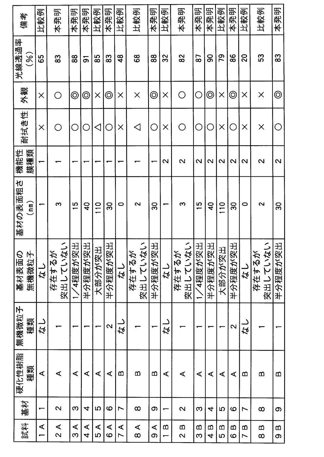
- the obtained samples 1A to 9A and 1B to 9B were put into a furnace at 260 ° C. for 10 minutes as a substitute for the reflow treatment, and then the following evaluation was performed.
- ⁇ No peeling is observed even after 100 times of wiping. ⁇ : No peeling is observed when the surface is wiped 30 times, but peeling is observed when the surface is wiped 100 times.
- the optical element sample having the configuration of the present invention is excellent in appearance without light transmittance, wiping resistance, cracks or peeling.
- Imaging device 1 Circuit board 2 Imaging module 3 Cover case 4 Imaging opening 5 Substrate module 6 Lens module 10 Sub board
Landscapes
- Physics & Mathematics (AREA)
- General Physics & Mathematics (AREA)
- Optics & Photonics (AREA)
- Compositions Of Macromolecular Compounds (AREA)
- Lens Barrels (AREA)
Abstract
Description
本発明で用いられる硬化性樹脂としては、紫外線及び電子線照射、あるいは加熱処理のいずれかの操作によって硬化し得るもので、無機微粒子と未硬化の状態で混合させた後、硬化させることによって透明な樹脂組成物を形成する物であれば特に制限なく使用でき、例えば、エポキシ樹脂、ビニルエステル樹脂、シリコーン樹脂、アクリル系樹脂、アリルエステル系樹脂等が挙げられる。該硬化性樹脂は紫外線や電子線等の照射を受けて硬化する活性光線硬化性樹脂であってもよいし、加熱処理によって硬化する熱硬化性樹脂であってもよく、例えば、下記に列記したような種類の樹脂を好ましく使用することができる。
Si-O-Siを主鎖としたシロキサン結合を有するシリコーン樹脂を使用することができる。当該シリコーン樹脂として、所定量のポリオルガノシロキサン樹脂よりなるシリコーン系樹脂が使用可能である(例えば特開平6-9937号公報参照)。
上記一般式(A)中、「R1」及び「R2」は同種又は異種の置換若しくは非置換の一価炭化水素基を示す。具体的には、「R1」及び「R2」として、メチル基、エチル基、プロピル基、ブチル基等のアルキル基、ビニル基、アリル基等のアルケニル基、フェニル基、トリル基等のアリール基、シクロヘキシル基、シクロオクチル基等のシクロアルキル基、またはこれらの基の炭素原子に結合した水素原子をハロゲン原子、シアノ基、アミノ基などで置換した基、例えばクロロメチル基、3,3,3-トリフルオロプロピル基、シアノメチル基、γ-アミノプロピル基、N-(β-アミノエチル)-γ-アミノプロピル基などが例示される。「R1」及び「R2」は水酸基及びアルコキシ基から選択される基であってもよい。また、上記一般式(A)中、「n」は50以上の整数を示す。
2-アルキル-2-アダマンチル(メタ)アクリレート(特開2002-193883号公報参照)、3,3′-ジアルコキシカルボニル-1,1′ビアダマンタン(特開2001-253835号公報参照)、1,1′-ビアダマンタン化合物(米国特許第3342880号明細書参照)、テトラアダマンタン(特開2006-169177号公報参照)、2-アルキル-2-ヒドロキシアダマンタン、2-アルキレンアダマンタン、1,3-アダマンタンジカルボン酸ジ-tert-ブチル等の芳香環を有しないアダマンタン骨格を有する硬化性樹脂(特開2001-322950号公報参照)、ビス(ヒドロキシフェニル)アダマンタン類やビス(グリシジルオキシフェニル)アダマンタン(特開平11-35522号公報、特開平10-130371号公報参照)等を使用することができる。
芳香環を含まない臭素含有(メタ)アリルエステル(特開2003-66201号公報参照)、アリル(メタ)アクリレート(特開平5-286896号公報参照)、アリルエステル樹脂(特開平5-286896号公報、特開2003-66201号公報参照)、アクリル酸エステルとエポキシ基含有不飽和化合物の共重合化合物(特開2003-128725号公報参照)、アクリレート化合物(特開2003-147072号公報参照)、アクリルエステル化合物(特開2005-2064号公報参照)等を好ましく用いることができる。
エポキシ化合物としては、例えば、ノボラックフェノール型エポキシ樹脂、ビフェニル型エポキシ樹脂、ジシクロペンタジエン型エポキシ樹脂、ビスフェノールFジグリシジルエーテル、ビスフェノールAジグリシジルエーテル、2,2′-ビス(4-グリシジルオキシシクロヘキシル)プロパン、3,4-エポキシシクロヘキシルメチル-3,4-エポキシシクロヘキサンカーボキシレート、ビニルシクロヘキセンジオキシド、2-(3,4-エポキシシクロヘキシル)-5,5-スピロ-(3,4-エポキシシクロヘキサン)-1,3-ジオキサン、ビス(3,4-エポキシシクロヘキシル)アジペート、1,2-シクロプロパンジカルボン酸ビスグリシジルエステル、トリグリシジルイソシアヌレート、モノアリルジグリシジルイソシアヌレート、ジアリルモノグリシジルイソシアヌレート等を挙げることができる。
本発明において用いられる無機微粒子としては、酸化物微粒子、金属塩微粒子、半導体微粒子などが挙げられるが、特に酸化物微粒子が好ましく用いられる。これらの中から、光学素子として使用する波長領域において吸収、発光、蛍光等が生じないものを適宜選択して使用することができる。
本発明は、前記硬化性樹脂と前記無機微粒子とを含有する基材であって、更に該無機微粒子が該基材の表面に存在することを特徴とする。ここでいう基材の表面とは、基材の最表面から1μmの深さまでの範囲をいい、この中に該無機微粒子が存在することにより、該基材の表面粗さが3nm以上100nm以下となることを特徴とする。また、該無機微粒子は、該基材の表面に突出していることが更に好ましい。本発明でいう「突出」とは、基材を形成する硬化性樹脂から無機微粒子が露出している状態をいう。
本発明の樹脂材料の調製時や樹脂組成物の成型工程においては、必要に応じて各種添加剤(配合剤ともいう)を添加することができる。添加剤については、格別限定はないが、酸化防止剤、熱安定剤、耐光安定剤、耐候安定剤、紫外線吸収剤、近赤外線吸収剤などの安定剤;滑剤、可塑剤などの樹脂改質剤;軟質重合体、アルコール性化合物等の白濁防止剤;染料や顔料などの着色剤;帯電防止剤、難燃剤、フィラーなどが挙げられる。これらの配合剤は、単独で、あるいは2種以上を組み合せて用いることができ、その配合量は本発明に記載の効果を損なわない範囲で適宜選択される。本発明においては、特に、上記樹脂組成物が少なくとも可塑剤または酸化防止剤を含有することが好ましい。
可塑剤としては、特に限定はないが、リン酸エステル系可塑剤、フタル酸エステル系可塑剤、トリメリット酸エステル系可塑剤、ピロメリット酸系可塑剤、グリコレート系可塑剤、クエン酸エステル系可塑剤、ポリエステル系可塑剤等を挙げることができる。
酸化防止剤としては、フェノール系酸化防止剤、リン系酸化防止剤、イオウ系酸化防止剤などが挙げられ、これらの中でもフェノール系酸化防止剤、特にアルキル置換フェノール系酸化防止剤が好ましい。これらの酸化防止剤を配合することにより、透明性、耐熱性等を低下させることなく、成型時の酸化劣化等によるレンズの着色や強度低下を防止できる。これらの酸化防止剤は、それぞれ単独で、あるいは2種以上を組み合わせて用いることができ、その配合量は、本発明の目的を損なわない範囲で適宜選択されるが、本発明に係る重合体100質量部に対して好ましくは0.001~5質量部、より好ましくは0.01~1質量部である。
耐光安定剤としては、ベンゾフェノン系耐光安定剤、ベンゾトリアゾール系耐光安定剤、ヒンダードアミン系耐光安定剤などが挙げられるが、本発明においては、レンズの透明性、耐着色性等の観点から、ヒンダードアミン系耐光安定剤を用いるのが好ましい。ヒンダードアミン系耐光安定剤(以下、HALSともいう)の中でも、テトラヒドロフラン(THF)を溶媒として用いたGPCにより測定したポリスチレン換算のMnが1000~10000であるものが好ましく、2000~5000であるものがより好ましく、2800~3800であるものが特に好ましい。Mnが小さすぎると、該HALSをブロック共重合体に加熱溶融混練して配合する際に、揮発のため所定量を配合できなかったり、射出成型等の加熱溶融成型時に発泡やシルバーストリークが生じるなど加工安定性が低下する。また、ランプを点灯させた状態でレンズを長時間使用する場合に、レンズから揮発性成分がガスとなって発生する。逆にMnが大き過ぎると、ブロック共重合体への分散性が低下して、レンズの透明性が低下し、耐光性改良の効果が低減する。したがって、本発明においては、HALSのMnを上記範囲とすることにより加工安定性、低ガス発生性、透明性に優れたレンズが得られる。
本発明の光学素子は、無機成分を主成分とする機能性層を有することを特徴とする。該機能性層とは、上術の通り成形された基材の表面に対し、無機成分を主成分とする膜が数層形成されたものをいう。
(i)透過光量の増加
光学素子の表面の反射率は屈折率に依存するが、BK-7のような低屈折率の硝材では4%、高屈折率硝材では8%にもなる。膜の種類にもよるが、コートした光学面は反射率が0.1~1%くらいになる。ズームレンズのように、レンズ枚数が多いと、膜の有無でレンズの透過率が大幅に変わる。反射防止膜を光学素子に形成すれば、反射率が低下するから当該光学素子を透過する光量が増加する。
「フレア、ゴースト」とは、光学系を通過する結像光(被写体の像を形成する光)以外の結像面に達する光のことであり、被写体以外のぼやけた像を形成したり、被写体像のコントラストを低下させる原因になる。反射防止膜を光学素子に形成すれば、これらフレア、ゴーストを減少させることができる。
カラー写真では色の再現性(カラーバランス)が重要な評価要素であり、光学素子の分光透過率が写真の色再現に大きな影響を与える。光学素子の分光透過率は、利用するコートの選び方により幾分か変えることができ、光学素子に反射防止膜を形成すればカラーバランスの調整が可能である。
(特にガラスレンズの場合)研磨し終えたままのレンズを長時間湿気の多い場所に放置しておくと、レンズの表面に白っぽい曇りを生じる。これを「ヤケ」と呼びレンズの光量低下の原因となる。反射防止膜はこのヤケを防ぐための有効な手段である。研磨後、きれいに洗浄したレンズにコートを行うとヤケは発生しない。コーティングによる膜の硬度はガラスよりかなり大きいので、光学素子を傷から護るのに有効である。この他、帯電性の緩和、外部環境変化の素子への影響を減少させる、など反射防止膜は光学素子の機械的、物理的及び化学的な安定性を高めている。
1層目:1.2≦n1≦1.55,60nm≦d1≦80nm
<2層構成:成形物/中又は高屈折率材料/低屈折率材料>
1層目:1.55≦n1,15nm≦d1≦91nm
2層目:1.2≦n2<1.55,30nm≦n2≦118
<3層構成:成形物/低屈折率材料/高屈折率材料/低屈折率材料>
1層目:1.2≦n1<1.55,10nm≦d1≦15000nm
2層目:1.7≦n2,20nm≦d2≦110nm
3層目:1.2≦n3<1.55,35nm≦d3≦90nm
<3層構成:成形物/中屈折率材料/高屈折率材料/低屈折率材料>
1層目:1.55≦n1<1.7,40nm≦d1≦15000nm
2層目:1.7≦n2,35nm≦d2≦90nm
3層目:1.2≦n3<1.55,45nm≦d3≦85nm
<5層構成:低又は中屈折率材料/高屈折率材料/低屈折率材料/高屈折率材料/低屈折率材料>
1層目:1.2≦n1<1.7,5nm≦d1≦15000nm
2層目:1.7≦n2,15nm≦d2≦35nm
3層目:1.2≦n3<1.55,25nm≦d3≦45nm
4層目:1.7≦n4,50nm≦d4≦130nm
5層目:1.2≦n5<1.55,80nm≦d5≦110
<7層構成:成形物/低又は中屈折率材料/高屈折率材料/低屈折率材料/高屈折率材料/低屈折率材料/高屈折率材料/低屈折率材料>
1層目:1.2≦n1<1.7,80nm≦d1≦15000nm
2層目:1.7≦n2,10nm≦d2≦25nm
3層目:1.2≦n3<1.55,30nm≦d3≦45nm
4層目:1.7≦n4,40nm≦d4≦60nm
5層目:1.2≦n5<1.55,10nm≦d5≦20nm
6層目:1.7≦n6,6nm≦d6≦70nm
7層目:1.2≦n7<1.55,60nm≦d7≦100
反射防止膜は上記の層構成に限定されず、4層構成、6層構成、8層構成又はそれ以上の層構成を有していてもよい。
なお、本実施形態に係る光学素子は、例えば下記のような光学部品に応用される。
<無機微粒子1の作製>
始めに、TM-300(大明化学製γアルミナ,一次粒子径7nm)23gに対して、純水500g、アンモニア水(関東化学28%)4.8gを加え攪拌した。この溶液をウルトラアペックスミルUAM-015(寿工業株式会社製)で、0.05mmビーズを用いて、周速7m/secで4時間分散した。この際、当該溶液に対してテトラエトキシシラン(信越化学製LS-2430)11.5gを2時間かけて滴下した。
新中村化学製 NKエステル DCP(トリシクロデカンジメタノールジメタクリレート)に重合開始剤として日本油脂製 パーブチルOを1質量%添加し、その混合物を熱硬化性樹脂Aとした。これを150℃、10Torr、真空下でプレスして、10分間硬化させ、直径11mm、厚さ3mmのテストピース(円板状成形物)を作製し、これを「基材1」とした。
基材1の作製で使用した熱硬化性樹脂Aと無機微粒子1とを予め乳鉢で混合し、その後、ラボプラストミル(株式会社東洋精機製作所製ラボプラストミルKF-6V)を用いて、上記混合物を加熱せずに混練した。この際、無機微粒子1の体積濃度が5vol%となるように、熱硬化性樹脂Aと無機微粒子1の添加量を調整した。
基材2の作製において、無機微粒子1の体積濃度が15vol%となるようにした以外は、基材2の作製と同じ方法で、「基材3」を作製した。
基材2の作製において、無機微粒子1の体積濃度が25vol%となるようにした以外は、基材2の作製と同じ方法で、「基材4」を作製した。
基材2の作製において、無機微粒子1の体積濃度が35vol%となるようにした以外は、基材2の作製と同じ方法で、「基材5」を作製した。
基材4の作製において、無機微粒子1を無機微粒子2(日本アエロジル社製シリカ粒子 RX300 一次粒子径7nm)に変えた以外は、基材4の作製と同じ方法で、「基材6」を作製した。
ダイセル株式会社製芳香族含有エポキシ樹脂と硬化剤として大日本インキ化学工業株式会社製 酸無水物 EPICLON B-650を各当量で混合し、その混合物を熱硬化性樹脂Bとした。これを160℃、10Torr、真空下でプレスして、10分間硬化させ、直径11mm、厚さ3mmのテストピース(円板状成形物)を作製し、これを「基材7」とした。
基材7の作製で使用した熱硬化性樹脂Bと、無機微粒子1とを予め乳鉢で混合し、その後、ラボプラストミルを用いて、上記混合物を加熱せずに混練した。この際、無機微粒子1の体積濃度が5vol%となるように、熱硬化性樹脂Bと無機微粒子1の添加量を調整した。
基材8の作製において、無機微粒子1の体積濃度が15vol%となるようにした以外は、基材8の作製と同じ方法で、「基材9」を作製した。
基材1~9の片面に、機能性層である反射防止膜を蒸着法で形成した。表1に示す条件で1層の反射防止膜を形成した試料を、それぞれ試料1A~9Aとし、表2に示す条件で5層の反射防止膜を形成した(1層目がテストピースに直に形成した膜である。)試料を、それぞれ試料1B~9Bとした。


得られた基材1~9について、AFM:WA-200(日立建機ファインテック製)を使用して表面の粗さを測定した。基準長さは1μmとした。
イソプロピルアルコールを染み込ませた綿棒で各サンプルの反射防止膜を形成した面を荷重5~10gで多数回拭いた。10回拭くごとに各サンプルの反射防止膜の成膜面を顕微鏡で観察し、反射防止膜の剥離の有無を観察した。そして、反射防止膜が剥離したときの拭き回数の合計で各サンプルの耐拭き性を評価した。その評価結果を表3に示す。表3中、○、△、×の基準は下記の通りとした。
△:30回拭いた時点では剥離は認められないが、100回拭いた時点では剥離が認められる
×:30回拭いた時点で剥離が認められる。
各サンプルの反射防止膜を形成した面の外観を顕微鏡で観察した。260℃で10分処理した後と、260℃,10分の処理を2回実施した後について、室温で反射防止膜を顕微鏡で観察した。その評価結果を表3に示す。表3中、◎,○,×の基準は下記の通りとした。
○:260℃処理2回においてはクラック又は剥離が認められる
×:260℃処理1回、260℃処理2回のいずれにおいてもクラック又は剥離が認められる
[光線透過率の評価]
各サンプルについて、ASTM D1003に準拠した方法で、東京電色(株)製のTURBIDITY METER T-2600DAを用いて光線透過率を測定した。その測定結果を表3に示す。
1 回路基板
2 撮像モジュール
3 カバーケース
4 撮像用開口
5 基板モジュール
6 レンズモジュール
10 サブ基板
10a 装着孔
11 CCDイメージセンサ
12 樹脂
15 レンズケース
15a ホルダ部
15b 装着部
16 レンズ
17 カラー部材
18 導電性材料
Claims (5)
- 硬化性樹脂と無機微粒子を含有する基材の表面に無機成分を主成分とする機能性層を有する光学素子であって、該基材の表面に少なくとも1種の無機微粒子が存在し、表面粗さが3nm以上100nm以下であることを特徴とする光学素子。
- 前記基材の表面粗さが、5nm以上50nm以下であることを特徴とする請求項1に記載の光学素子。
- 前記基材の表面に無機微粒子が突出していることを特徴とする請求項1または2に記載の光学素子。
- 電子部品とともにリフロー処理により基板に実装される撮像装置に用いられることを特徴とする請求項1~3のいずれか1項に記載の光学素子。
- 請求項1~4のいずれか1項に記載の光学素子を有する撮像装置を電子部品とともに基板上に載置する工程、及び、前記撮像装置と、前記電子部品と、前記基板とをリフロー処理に供し、前記撮像装置と前記電子部品とを前記基板に実装する工程、を有することを特徴とする電子機器の製造方法。
Priority Applications (2)
| Application Number | Priority Date | Filing Date | Title |
|---|---|---|---|
| JP2010512989A JPWO2009142124A1 (ja) | 2008-05-22 | 2009-05-12 | 光学素子、及びそれを用いた電子機器の製造方法 |
| US12/993,442 US20110070402A1 (en) | 2008-05-22 | 2009-05-12 | Optical Element, and Process for Producing Electronic Equipment using the Optical Element |
Applications Claiming Priority (2)
| Application Number | Priority Date | Filing Date | Title |
|---|---|---|---|
| JP2008134066 | 2008-05-22 | ||
| JP2008-134066 | 2008-05-22 |
Publications (1)
| Publication Number | Publication Date |
|---|---|
| WO2009142124A1 true WO2009142124A1 (ja) | 2009-11-26 |
Family
ID=41340056
Family Applications (1)
| Application Number | Title | Priority Date | Filing Date |
|---|---|---|---|
| PCT/JP2009/058823 Ceased WO2009142124A1 (ja) | 2008-05-22 | 2009-05-12 | 光学素子、及びそれを用いた電子機器の製造方法 |
Country Status (3)
| Country | Link |
|---|---|
| US (1) | US20110070402A1 (ja) |
| JP (1) | JPWO2009142124A1 (ja) |
| WO (1) | WO2009142124A1 (ja) |
Families Citing this family (1)
| Publication number | Priority date | Publication date | Assignee | Title |
|---|---|---|---|---|
| US20150116576A1 (en) * | 2013-10-30 | 2015-04-30 | Blackberry Limited | Image capture assembly, digital camera and a mobile device having an improved construction |
Citations (3)
| Publication number | Priority date | Publication date | Assignee | Title |
|---|---|---|---|---|
| JP2003183414A (ja) * | 2001-12-13 | 2003-07-03 | Mitsubishi Chemicals Corp | 超微粒子を含有する架橋樹脂組成物成形体 |
| WO2007102299A1 (ja) * | 2006-03-08 | 2007-09-13 | Konica Minolta Opto, Inc. | 光学素子 |
| JP2008088303A (ja) * | 2006-10-02 | 2008-04-17 | Sumitomo Electric Fine Polymer Inc | 透明樹脂成形体並びに光学レンズ及び光学フィルム |
-
2009
- 2009-05-12 WO PCT/JP2009/058823 patent/WO2009142124A1/ja not_active Ceased
- 2009-05-12 US US12/993,442 patent/US20110070402A1/en not_active Abandoned
- 2009-05-12 JP JP2010512989A patent/JPWO2009142124A1/ja active Pending
Patent Citations (3)
| Publication number | Priority date | Publication date | Assignee | Title |
|---|---|---|---|---|
| JP2003183414A (ja) * | 2001-12-13 | 2003-07-03 | Mitsubishi Chemicals Corp | 超微粒子を含有する架橋樹脂組成物成形体 |
| WO2007102299A1 (ja) * | 2006-03-08 | 2007-09-13 | Konica Minolta Opto, Inc. | 光学素子 |
| JP2008088303A (ja) * | 2006-10-02 | 2008-04-17 | Sumitomo Electric Fine Polymer Inc | 透明樹脂成形体並びに光学レンズ及び光学フィルム |
Also Published As
| Publication number | Publication date |
|---|---|
| US20110070402A1 (en) | 2011-03-24 |
| JPWO2009142124A1 (ja) | 2011-09-29 |
Similar Documents
| Publication | Publication Date | Title |
|---|---|---|
| CN101591472B (zh) | 可固化树脂材料组合物,光学材料,发光器件,制备发光器件的方法,和电子器件 | |
| CN101114107B (zh) | 成像设备 | |
| JP6606626B1 (ja) | 光学フィルタ及び光学フィルタ用組成物 | |
| JP2017032685A (ja) | 光学フィルターおよび光学フィルターを用いた装置 | |
| JP2007291321A (ja) | 硬化型有機金属組成物及び有機金属ポリマー材料並びに光学部品 | |
| JP2017072748A (ja) | 光学フィルターおよび光学フィルターを用いた撮像素子 | |
| TW201634588A (zh) | 光學機能層形成用組成物、利用該光學機能層形成用組成物之固體攝像元件以及相機模組 | |
| JP2009251093A (ja) | 光学用複合材料、及び光学素子 | |
| JP2008266578A (ja) | 光学ポリマー材料及び光学部品 | |
| Lee et al. | Zirconia nanocomposites and their applications as transparent advanced optical materials with high refractive index | |
| US9285507B2 (en) | High-refractive composition | |
| WO2009142124A1 (ja) | 光学素子、及びそれを用いた電子機器の製造方法 | |
| WO2009087836A1 (ja) | 光学素子の製造方法、光学素子、電子機器の製造方法及び電子機器 | |
| US20090244729A1 (en) | Method for manufacturing optical element, optical element unit, and imaging unit | |
| US20080233417A1 (en) | Optical polymer material and optical component | |
| JP2009235325A (ja) | 光学用樹脂材料の製造方法、光学用樹脂材料、及び光学素子 | |
| US20100219541A1 (en) | Method for manufacturing optical device | |
| US7582358B2 (en) | Organic-inorganic composite forming material, organic-inorganic composite, production method thereof and optical element | |
| JP2009265562A (ja) | 光学素子、及びそれを実装した電子機器の製造方法 | |
| JP2009237471A (ja) | 光学用樹脂材料とその製造方法及び光学素子 | |
| JP2009173820A (ja) | 有機無機複合樹脂材料、その製造方法、およびそれを用いた光学素子 | |
| JP2009084459A (ja) | 光学用有機無機複合材料、光学用有機無機複合材料の製造方法、及び光学素子 | |
| JP2010018700A (ja) | 光学素子、及び電子機器の製造方法 | |
| CN103364851A (zh) | 光学元件、摄像装置、电子设备以及光学元件的制造方法 | |
| JP2011247925A (ja) | 複合光学素子、複合光学素子の製造方法、複合光学素子を備えた撮像装置および複合光学素子を備えた光学式記録再生装置 |
Legal Events
| Date | Code | Title | Description |
|---|---|---|---|
| 121 | Ep: the epo has been informed by wipo that ep was designated in this application |
Ref document number: 09750486 Country of ref document: EP Kind code of ref document: A1 |
|
| WWE | Wipo information: entry into national phase |
Ref document number: 2010512989 Country of ref document: JP |
|
| WWE | Wipo information: entry into national phase |
Ref document number: 12993442 Country of ref document: US |
|
| NENP | Non-entry into the national phase |
Ref country code: DE |
|
| 122 | Ep: pct application non-entry in european phase |
Ref document number: 09750486 Country of ref document: EP Kind code of ref document: A1 |