WO2009133682A1 - Evaluation method and evaluation device - Google Patents
Evaluation method and evaluation device Download PDFInfo
- Publication number
- WO2009133682A1 WO2009133682A1 PCT/JP2009/001886 JP2009001886W WO2009133682A1 WO 2009133682 A1 WO2009133682 A1 WO 2009133682A1 JP 2009001886 W JP2009001886 W JP 2009001886W WO 2009133682 A1 WO2009133682 A1 WO 2009133682A1
- Authority
- WO
- WIPO (PCT)
- Prior art keywords
- substrate
- evaluation
- relative position
- displacement
- weighting
- Prior art date
Links
Images


Classifications
-
- H—ELECTRICITY
- H01—ELECTRIC ELEMENTS
- H01L—SEMICONDUCTOR DEVICES NOT COVERED BY CLASS H10
- H01L23/00—Details of semiconductor or other solid state devices
- H01L23/544—Marks applied to semiconductor devices or parts, e.g. registration marks, alignment structures, wafer maps
-
- H—ELECTRICITY
- H01—ELECTRIC ELEMENTS
- H01L—SEMICONDUCTOR DEVICES NOT COVERED BY CLASS H10
- H01L22/00—Testing or measuring during manufacture or treatment; Reliability measurements, i.e. testing of parts without further processing to modify the parts as such; Structural arrangements therefor
- H01L22/10—Measuring as part of the manufacturing process
- H01L22/12—Measuring as part of the manufacturing process for structural parameters, e.g. thickness, line width, refractive index, temperature, warp, bond strength, defects, optical inspection, electrical measurement of structural dimensions, metallurgic measurement of diffusions
-
- H—ELECTRICITY
- H01—ELECTRIC ELEMENTS
- H01L—SEMICONDUCTOR DEVICES NOT COVERED BY CLASS H10
- H01L24/00—Arrangements for connecting or disconnecting semiconductor or solid-state bodies; Methods or apparatus related thereto
- H01L24/80—Methods for connecting semiconductor or other solid state bodies using means for bonding being attached to, or being formed on, the surface to be connected
- H01L24/81—Methods for connecting semiconductor or other solid state bodies using means for bonding being attached to, or being formed on, the surface to be connected using a bump connector
-
- H—ELECTRICITY
- H01—ELECTRIC ELEMENTS
- H01L—SEMICONDUCTOR DEVICES NOT COVERED BY CLASS H10
- H01L25/00—Assemblies consisting of a plurality of individual semiconductor or other solid state devices ; Multistep manufacturing processes thereof
- H01L25/50—Multistep manufacturing processes of assemblies consisting of devices, each device being of a type provided for in group H01L27/00 or H01L29/00
-
- H—ELECTRICITY
- H01—ELECTRIC ELEMENTS
- H01L—SEMICONDUCTOR DEVICES NOT COVERED BY CLASS H10
- H01L2223/00—Details relating to semiconductor or other solid state devices covered by the group H01L23/00
- H01L2223/544—Marks applied to semiconductor devices or parts
- H01L2223/5442—Marks applied to semiconductor devices or parts comprising non digital, non alphanumeric information, e.g. symbols
-
- H—ELECTRICITY
- H01—ELECTRIC ELEMENTS
- H01L—SEMICONDUCTOR DEVICES NOT COVERED BY CLASS H10
- H01L2223/00—Details relating to semiconductor or other solid state devices covered by the group H01L23/00
- H01L2223/544—Marks applied to semiconductor devices or parts
- H01L2223/54426—Marks applied to semiconductor devices or parts for alignment
-
- H—ELECTRICITY
- H01—ELECTRIC ELEMENTS
- H01L—SEMICONDUCTOR DEVICES NOT COVERED BY CLASS H10
- H01L2223/00—Details relating to semiconductor or other solid state devices covered by the group H01L23/00
- H01L2223/544—Marks applied to semiconductor devices or parts
- H01L2223/54453—Marks applied to semiconductor devices or parts for use prior to dicing
-
- H—ELECTRICITY
- H01—ELECTRIC ELEMENTS
- H01L—SEMICONDUCTOR DEVICES NOT COVERED BY CLASS H10
- H01L2224/00—Indexing scheme for arrangements for connecting or disconnecting semiconductor or solid-state bodies and methods related thereto as covered by H01L24/00
- H01L2224/80—Methods for connecting semiconductor or other solid state bodies using means for bonding being attached to, or being formed on, the surface to be connected
- H01L2224/81—Methods for connecting semiconductor or other solid state bodies using means for bonding being attached to, or being formed on, the surface to be connected using a bump connector
- H01L2224/8112—Aligning
- H01L2224/81121—Active alignment, i.e. by apparatus steering, e.g. optical alignment using marks or sensors
- H01L2224/8113—Active alignment, i.e. by apparatus steering, e.g. optical alignment using marks or sensors using marks formed on the semiconductor or solid-state body
-
- H—ELECTRICITY
- H01—ELECTRIC ELEMENTS
- H01L—SEMICONDUCTOR DEVICES NOT COVERED BY CLASS H10
- H01L2224/00—Indexing scheme for arrangements for connecting or disconnecting semiconductor or solid-state bodies and methods related thereto as covered by H01L24/00
- H01L2224/80—Methods for connecting semiconductor or other solid state bodies using means for bonding being attached to, or being formed on, the surface to be connected
- H01L2224/81—Methods for connecting semiconductor or other solid state bodies using means for bonding being attached to, or being formed on, the surface to be connected using a bump connector
- H01L2224/8112—Aligning
- H01L2224/81121—Active alignment, i.e. by apparatus steering, e.g. optical alignment using marks or sensors
- H01L2224/81132—Active alignment, i.e. by apparatus steering, e.g. optical alignment using marks or sensors using marks formed outside the semiconductor or solid-state body, i.e. "off-chip"
-
- H—ELECTRICITY
- H01—ELECTRIC ELEMENTS
- H01L—SEMICONDUCTOR DEVICES NOT COVERED BY CLASS H10
- H01L2225/00—Details relating to assemblies covered by the group H01L25/00 but not provided for in its subgroups
- H01L2225/03—All the devices being of a type provided for in the same subgroup of groups H01L27/00 - H01L33/648 and H10K99/00
- H01L2225/04—All the devices being of a type provided for in the same subgroup of groups H01L27/00 - H01L33/648 and H10K99/00 the devices not having separate containers
- H01L2225/065—All the devices being of a type provided for in the same subgroup of groups H01L27/00 - H01L33/648 and H10K99/00 the devices not having separate containers the devices being of a type provided for in group H01L27/00
- H01L2225/06503—Stacked arrangements of devices
- H01L2225/06513—Bump or bump-like direct electrical connections between devices, e.g. flip-chip connection, solder bumps
-
- H—ELECTRICITY
- H01—ELECTRIC ELEMENTS
- H01L—SEMICONDUCTOR DEVICES NOT COVERED BY CLASS H10
- H01L2924/00—Indexing scheme for arrangements or methods for connecting or disconnecting semiconductor or solid-state bodies as covered by H01L24/00
- H01L2924/01—Chemical elements
- H01L2924/01004—Beryllium [Be]
-
- H—ELECTRICITY
- H01—ELECTRIC ELEMENTS
- H01L—SEMICONDUCTOR DEVICES NOT COVERED BY CLASS H10
- H01L2924/00—Indexing scheme for arrangements or methods for connecting or disconnecting semiconductor or solid-state bodies as covered by H01L24/00
- H01L2924/01—Chemical elements
- H01L2924/01005—Boron [B]
-
- H—ELECTRICITY
- H01—ELECTRIC ELEMENTS
- H01L—SEMICONDUCTOR DEVICES NOT COVERED BY CLASS H10
- H01L2924/00—Indexing scheme for arrangements or methods for connecting or disconnecting semiconductor or solid-state bodies as covered by H01L24/00
- H01L2924/01—Chemical elements
- H01L2924/01033—Arsenic [As]
Definitions
- the present invention relates to an evaluation method and an evaluation apparatus for evaluating a substrate stacking apparatus.
- This application is related to the following Japanese application. For designated countries where incorporation by reference of documents is permitted, the contents described in the following application are incorporated into this application by reference and made a part of this application.
- the semiconductor manufacturing apparatus that manufactures a three-dimensional mounting semiconductor device by stacking wafers, which are substrates on which a plurality of semiconductor devices are formed.
- the semiconductor manufacturing apparatus includes an alignment apparatus and a stacking apparatus.
- the positioning device positions a plurality of wafers to be stacked with each other.
- the stacking apparatus heats and pressurizes the plurality of wafers positioned with respect to each other by the positioning apparatus to stack them.
- a pre-measuring step of measuring a relative position of the first substrate and the second substrate positioned with respect to each other before superposition A post-measurement step of measuring a relative position between the first substrate and the second substrate after the substrate and the second substrate are superposed on each other by the substrate superposing device; and a relative position measured in the pre-measuring step
- an evaluation method including an evaluation step of evaluating the substrate overlaying apparatus using the relative position measured in the post-measurement step.
- a pre-measuring unit that measures a relative position of the first substrate and the second substrate that are positioned with each other before being overlapped, and the first substrate and the second substrate.
- a post-measuring unit that measures the relative position between the first substrate and the second substrate after being superposed on each other by the substrate superposing device, a relative position that is measured by the front measuring unit, and a relative that is measured by the rear measuring unit
- An evaluation device is provided that includes an evaluation unit that evaluates the substrate overlaying device using the position.
- the top view of the wafer 90 for evaluation used for the evaluation method of this embodiment is shown.
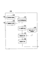
- the functional block diagram of the evaluation apparatus 310 of this embodiment is shown. The flow of each process of the evaluation method of this embodiment is shown.
- An example of the mark 92 and the mark 94 is shown.
- the top view of the other wafer 90 for evaluation used for the evaluation method of this embodiment is shown.
- the evaluation method according to the present embodiment is an evaluation method for evaluating a substrate overlaying apparatus that superimposes a plurality of substrates, and is intended to evaluate the dispersibility of a displacement pattern, that is, a dimensional strain within the substrate surface.
- an object of the present invention is to reduce the resulting shift amount by evaluating the magnitude of the influence of each displacement pattern on the shift amount due to heating and pressurization after alignment.
- FIG. 1 is a side view showing an outline of a positioning device 100 used in the evaluation method of the present embodiment.
- the positioning apparatus 100 positions and overlaps a wafer holder 50 that holds a wafer 10 as an example of a substrate and a wafer holder 70 that holds a wafer 30 as an example of a substrate. Thereby, the wafers 10 and 30 are held between the wafer holders 50 and 70.
- the microscope 130 of the positioning device 100 includes a mark 20 provided on the wafer 10 from an observation hole 52 provided in the wafer holder 50 arranged on the microscope 130 side, that is, the upper side in the drawing.
- the wafer 10 and the wafer 30 are positioned by observing the mark 40 provided on the wafer 30.
- the holder mark 60 provided on the wafer holder 50 and the holder mark 80 provided on the wafer holder 70 are observed with the microscope 130. It may be positioned. In this case, the relative position between the mark 20 on the wafer 10 and the holder mark 80 on the wafer holder 50 is observed in advance by the microscope 130, and the relative position between the mark 40 on the wafer 30 and the holder mark 80 on the wafer holder 70 is compared. By observing the position with the microscope 130 in advance, as a result, the wafer 10 and the wafer 30 can be positioned.
- FIG. 2 is a schematic diagram showing an outline of a heating and pressing apparatus 200 that is an object of the evaluation method of the present embodiment.
- the heating and pressing apparatus 200 stacks the wafer 10 and the wafer 30 held by the wafer holders 50 and 70 by pressing and heating the wafer holders 50 and 70 that are positioned and overlapped with each other.
- pressurization and heating are examples of superposition
- the heating and pressurizing apparatus 200 is an example of a substrate superposition apparatus.
- the wafer holders 50 and 70 are pressurized by the heaters 250 and 260 while heating the upper press 230 and the lower press 240 with a predetermined temperature profile. Thereby, the electrodes of the respective semiconductor devices on the wafer 10 are bonded.
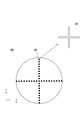
- FIG. 3 is a plan view of an evaluation wafer 90 used in the evaluation method of the present embodiment.
- the evaluation wafer 90 has the same outer shape as the wafer 10 and the like used in the positioning device 100 and the heating and pressing device 200.
- the outer diameter of the evaluation wafer 90 is 200 mm.
- a plurality of marks 92 are formed on the evaluation wafer 90, but a wafer on which a semiconductor device is formed may be used.
- the evaluation wafer 90 has a total of 37 marks 92 arranged in a line in the horizontal direction in the drawing, that is, the X direction, and the vertical direction, that is, the Y direction. These vertical and horizontal rows intersect at the center of the evaluation wafer 90.
- the wafer 10 may be used by providing the mark 92 on the wafer 10 provided with a plurality of semiconductor devices.
- the mark 92 has a cross shape in which a line segment extending in the X direction and a line segment extending in the Y direction are orthogonal to each other, as shown in an enlarged manner in the upper right of FIG.
- the length of each line segment of the mark 92 is 2 mm
- the line width of each line segment is 20 ⁇ m. This size is determined by the magnification and field of view of the optical microscope to be detected, the resolution of the imaging device, etc., and is not limited to this size.
- the mark 92 is formed by using, for example, a part of a process for forming a semiconductor device on the wafer 10.
- the shape of the mark 92 is not limited to the cross shape, and may be other shapes such as a circle and a rectangle.
- FIG. 4 shows a functional block diagram of the evaluation apparatus 310 of this embodiment
- FIG. 5 shows a flow of each process of the evaluation method of the evaluation apparatus 310.
- 4 includes a pre-stack measurement unit 320, a post-stack measurement unit 330, a relative position storage unit 340, a deviation amount calculation unit 350, a displacement pattern storage unit 360, a coefficient calculation unit 370, and a coefficient output unit 380.
- the function of the evaluation apparatus 310 will be described with reference to FIGS. 4 and 5.
- the evaluation method first, it is started by positioning by the positioning device 100 (S100).
- step S100 the evaluation wafers 90 are respectively held by the wafer holders 50 and 70 shown in FIG. 1, and the upper and lower evaluation wafers 90 are positioned relative to each other by the positioning device 100 using the above method.
- the pre-stack measurement unit 320 of the evaluation apparatus 310 performs a process before stacking the upper evaluation wafer 90 held by the upper wafer holder 50 and the lower evaluation wafer 90 held by the lower wafer holder 70.
- the relative position is measured (S110). Further, the pre-stack measurement unit 320 stores the relative position in the relative position storage unit 340.
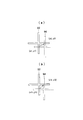
- FIG. 6A shows an example of the mark 92 and the mark 94 measured in step S110.
- step S110 the mark 92 provided on the upper evaluation wafer 90 and the lower evaluation wafer 90 positioned with respect to the upper evaluation wafer 90, The relative positions of the marks 94 provided at the positions corresponding to the respective marks 92 are measured.
- the deviation (x 2 ⁇ x 1 , y 2 ⁇ y 1 ) is measured as a relative position at the measurement point.
- step S110 the relative positions of the pairs of marks 92 and 94 corresponding to each other on the upper and lower evaluation wafers 90 are measured.
- the pre-stack measurement unit 320 may measure the relative position using the microscope 130 of the positioning device 100, or may carry the measurement from the positioning device 100 to a separate microscope and perform measurement using the microscope.
- the pre-stack measurement unit 320 automatically measures an image captured by a microscope by performing image processing with a computer or the like.
- the heating and pressing apparatus 200 preferably stacks the upper and lower evaluation wafers 90 using the same pressing conditions and heating conditions as those for stacking the wafers 10 and the like on which the semiconductor devices are formed.
- dummy electrodes or thermoplastic resin columns may be provided at positions corresponding to each other on the upper and lower evaluation wafers 90. Good.
- the post-stack measurement unit 330 measures the relative position of the upper and lower evaluation wafers 90 after the stack (S130).
- FIG. 6B shows an example of the mark 92 and the mark 94 measured in step S130.
- the mark 92 on the upper evaluation wafer 90 after lamination and the lower evaluation wafer 90 are provided at positions corresponding to the respective marks 92 on the upper evaluation wafer 90.
- the relative position of the mark 94 is measured (S130).
- step S110 two intersections between the mark 92 and the mark 94 in the " ⁇ " type formed by intersection shifted and a mark 92 and the mark 94 (x'1, y'1) , (x' 2, y 'displacement of 2) (x'2 -x' 1, y'2 -y' 1) is measured as a relative position in the measurement point.
- step S130 the relative positions of the corresponding sets of marks 92 and 94 on the upper and lower evaluation wafers 90 are measured.
- the post-stacking measurement unit 330 may transport the evaluation wafer 90 after stacking to the positioning device 100 and measure the relative position using the microscope 130, or may transport the wafer to a microscope separate from the positioning device 100. And you may measure with the said microscope. Further, the post-stacking measurement unit 330 stores the relative position in the relative position storage unit 340.
- the deviation amount calculation unit 350 calculates the deviation amount between the relative position measured in step S110 and the relative position measured in step S130 (S140). In this case, the deviation amount calculation unit 350 reads the relative position stored in the relative position storage unit 340 and calculates the deviation amount. This shift amount indicates how much each measurement point of the upper and lower evaluation wafers 90 has shifted due to being stacked by S120 after being aligned by S100. The deviation amount is calculated by the following mathematical formula 1. Note that the subscript i indicates a value for the i-th mark 92 (and the corresponding mark 94).
- the coefficient calculation unit 370 calculates a weighting coefficient of the displacement pattern when the deviation amount calculated in step S140 is approximated by weighted addition of a plurality of known displacement patterns (S150).
- the plurality of displacement patterns include translation in the wafer plane, isotropic magnification, rotation, anisotropic magnification, and orthogonality.
- the weighting coefficients corresponding to the displacement pattern are respectively the X direction C 1 , the Y direction C 2 , the isotropic magnification C 3 , the rotation C 4 , the anisotropic magnification C 5, and the orthogonality of the translation in the wafer plane.
- the shift amount is expressed by the following formula 2.
- the weighting coefficient of each displacement pattern when each measurement point is displaced to a position that approximates the amount of deviation calculated in S140 is calculated.
- x and y are variables, and each weighting coefficient is calculated by the least square method so that the error of Equation 2 is minimized.
- the weighting coefficient can be calculated by a simple method.
- the displacement pattern is preferably associated with a factor that causes the displacement pattern.
- a factor that causes the displacement pattern For example, translation and rotation within the wafer are associated with factors such as contact during wafer transfer and loading into the heating and pressing apparatus 200.
- the isotropic magnification is related to the heating of the upper press 230 and the lower press 240
- the orthogonality and the anisotropic magnification are related to the heating and pressurization, particularly the temperature distribution of the upper press 230 and the lower press 240.
- a plurality of displacement patterns and a plurality of factors may be associated with each other, and in this case, they may be associated with each other in a matrix weighted manner. Information regarding these associations is stored in the displacement pattern storage unit 360.
- the coefficient output unit 380 outputs the weighting coefficient of each displacement pattern calculated in step S150 (S160). For example, when the weighting coefficient of each displacement pattern is calculated using a computer in step S150, the coefficient output unit 380 displays the weighting coefficient on the screen.
- linear displacement patterns are used as the plurality of displacement patterns, but the displacement patterns are not limited to this.
- a second-order or higher-order displacement pattern such as x 2 , xy, and x 3 may be used.
- Higher order displacement patterns include local deformation and the like.
- the mark 92 is provided in an oblique direction on the surface of the evaluation wafer 90 and over the entire surface of the evaluation wafer 90 as described above.
- step S160 the heating and pressing apparatus 200 can be evaluated by outputting the weighting coefficient corresponding to each displacement pattern.
- the weighting coefficients it is possible to recognize which displacement pattern greatly affects the deformation of each evaluation wafer 90 in the operation of the heating and pressing apparatus 200. For example, when one or more specific weighting factors are larger than other weighting factors, it can be recognized that a displacement pattern corresponding to the weighting factor appears greatly due to some specific factor. it can.
- the resulting deviation amount between the upper and lower evaluation wafers 90 is set within the set range based on the value of each weighting coefficient. Therefore, it can be understood which factor is necessary to change the semiconductor manufacturing apparatus including the heating / pressurizing apparatus 200 and the semiconductor manufacturing process to reduce the resulting shift amount. For example, if the value of the direction C 1 and the Y direction C 2 of the translation is large, because there is a factor in the transport system for transporting the wafer, it is understood that it is sufficient to adjust the transfer system.
- any of the above weighting factors is within the specified range, it may be evaluated that the heating and pressing apparatus 200 operates normally. For example, even if the resulting deviation amount is within the set range, it is conceivable that the deviation amounts due to several displacement modes are offset. During use of the heating and pressurizing apparatus 200, deviation amounts due to these displacement modes may occur in a direction in which they are not canceled out. In this case, the resulting deviation amounts do not fall within the set range.
- some weighting factors are outside the specified range. I understand that. Thereby, the said heating-pressing apparatus 200 can be evaluated more correctly.
- the evaluation wafer 90 shown in FIG. 7 may be used instead of the evaluation wafer shown in FIG.
- the evaluation wafer 90 shown in FIG. 7 has the same mark throughout the wafer.
- the evaluation device 310 may be a separate body from the positioning device 100 and the heating and pressing device 200, but may be incorporated in the positioning device 100 or the heating and pressing device 200. Furthermore, although the pre-stack measurement unit 320 and the post-stack measurement unit 330 in the evaluation device 310 have been described as separate blocks, the same functional block may be used. Note that the coefficient calculation step and the coefficient calculation unit 370 in the above embodiment are examples of a weighting step and a weighting unit, respectively.
- the mark provided on the silicon wafer may be detected by transmitting infrared light through the silicon wafer.
- a substrate made of a material that is transparent to visible light, such as glass is used as the evaluation wafer 90, the mark provided on the substrate may be detected by transmitting visible light to the substrate.
- the evaluation method and the evaluation apparatus of the above embodiment evaluate the heating and pressing apparatus 200 that pressurizes and heats the wafer 10 and the wafer 30.
- the evaluation method and the evaluation apparatus may evaluate the positioning apparatus 100 that positions the wafer 10 and the wafer 30 and sandwiches them between the wafer holders 50 and 70.
- overlapping the wafer 10 and the wafer 30 with the wafer holders 50 and 70 is an example of superposition
- the positioning device 100 is an example of a substrate superposition device. That is, in the pre-measurement step, the relative positions of the wafer 10 held by the wafer holder 50 and the wafer 30 held by the wafer holder 70 are positioned after the wafers 10 and 30 are positioned with each other. Measure before 70 overlaps.
- the wafer 10 and the wafer 30 sandwiched between the wafer holders 50 and 70 are transported inside or outside the positioning device 100 in a post-measurement process. Measure the relative position.
- the deformation pattern includes translation and rotation of the wafer. The translation and rotation of these wafers are for the pressure when the wafers come into contact with each other, the accuracy when the stage of the positioning apparatus 100 moves in the Z direction, the detection accuracy of the wafer marks, and the relative ground measurement after the wafer holders are overlaid. It is related to the transportation etc.
Abstract
Provided is an evaluation method which evaluates a degree of in-plane deformation of a substrate in a substrate layering device. The evaluation method includes: a pre-measurement step which measures a relative position of a first substrate and a second substrate which have been mutually positioned before superposition; a post-measurement step which measures a relative position of the first substrate and the second substrate after mutual superposition of the first substrate and the second substrate by a substrate superposing device; and an evaluation step which evaluates the substrate superposing device by using the relative position obtained in the pre-measurement step and the relative position obtained in the post-measurement step.
Description
本発明は、基板積層装置を評価する評価方法および評価装置に関する。なお、本出願は、下記の日本出願に関連する。文献の参照による組み込みが認められる指定国については、下記の出願に記載された内容を参照により本出願に組み込み、本出願の一部とする。
特願2008-119114 出願日2008年4月30日 The present invention relates to an evaluation method and an evaluation apparatus for evaluating a substrate stacking apparatus. This application is related to the following Japanese application. For designated countries where incorporation by reference of documents is permitted, the contents described in the following application are incorporated into this application by reference and made a part of this application.
Japanese Patent Application No. 2008-119114 Filing Date April 30, 2008
複数の半導体装置が形成された基板であるウエハを積層して三次元実装半導体装置を製造する半導体製造装置がある。当該半導体製造装置は、位置合わせ装置と積層装置とを有する。位置決め装置は、積層されるべき複数のウエハを互いに位置決めする。また、積層装置は、位置決め装置によって互いに位置決めされた当該複数のウエハを加熱および加圧して積層する。
There is a semiconductor manufacturing apparatus that manufactures a three-dimensional mounting semiconductor device by stacking wafers, which are substrates on which a plurality of semiconductor devices are formed. The semiconductor manufacturing apparatus includes an alignment apparatus and a stacking apparatus. The positioning device positions a plurality of wafers to be stacked with each other. The stacking apparatus heats and pressurizes the plurality of wafers positioned with respect to each other by the positioning apparatus to stack them.
ここで、積層装置は加熱および加圧によってウエハを積層するので、当該加熱および加圧によって、ウエハが変形するという課題がある。当該課題に対し、ウエハの変形を予め見込んだ位置に各半導体装置を設ける半導体製造方法がある(例えば、特許文献1を参照)。
Here, since the stacking apparatus stacks the wafers by heating and pressing, there is a problem that the wafers are deformed by the heating and pressing. In order to solve this problem, there is a semiconductor manufacturing method in which each semiconductor device is provided at a position where the deformation of the wafer is expected in advance (see, for example, Patent Document 1).
しかしながら、上記特許文献1の半導体製造方法においては、ウエハの熱膨張の等方倍率による変形を予め見込むものであって、熱膨張以外の変形については考慮されていない。ここで、熱膨張以外に、積層装置による積層において様々な要因による変形があるが、これらの要因による変形は上下ウエハの結果としてのずれ量として現れるので、個別の要因によってどの程度の変形が生じているかを評価することは困難であった。よって、当該変形によるずれ量を低減することは困難であった。
However, in the semiconductor manufacturing method of Patent Document 1 described above, deformation due to isotropic magnification of the thermal expansion of the wafer is expected in advance, and deformation other than thermal expansion is not considered. Here, in addition to thermal expansion, there are deformations due to various factors in the laminating by the laminating apparatus, but deformation due to these factors appears as a deviation amount as a result of the upper and lower wafers, so how much deformation occurs due to individual factors. It was difficult to assess whether Therefore, it has been difficult to reduce the amount of deviation due to the deformation.
上記課題を解決するために、本発明の第1の形態においては、互いに位置決めされた第1の基板と第2の基板との重ね合わせ前の相対位置を計測する前計測工程と、第1の基板と第2の基板とを基板重ね合わせ装置により互いに重ね合わせた後の、第1の基板と第2の基板との相対位置を計測する後計測工程と、前計測工程で計測した相対位置と、後計測工程で計測した相対位置とを用いて基板重ね合わせ装置を評価する評価工程とを備える評価方法が提供される。
In order to solve the above-described problem, in the first embodiment of the present invention, a pre-measuring step of measuring a relative position of the first substrate and the second substrate positioned with respect to each other before superposition, A post-measurement step of measuring a relative position between the first substrate and the second substrate after the substrate and the second substrate are superposed on each other by the substrate superposing device; and a relative position measured in the pre-measuring step There is provided an evaluation method including an evaluation step of evaluating the substrate overlaying apparatus using the relative position measured in the post-measurement step.
本発明の第2の形態においては、互いに位置決めされた第1の基板と第2の基板との重ね合わせ前の相対位置を計測する前計測部と、第1の基板と第2の基板とを基板重ね合わせ装置により互いに重ね合わせた後の、第1の基板と第2の基板との相対位置を計測する後計測部と、前計測部で計測した相対位置と、後計測部で計測した相対位置とを用いて基板重ね合わせ装置を評価する評価部とを備える評価装置が提供される。
In the second embodiment of the present invention, a pre-measuring unit that measures a relative position of the first substrate and the second substrate that are positioned with each other before being overlapped, and the first substrate and the second substrate. A post-measuring unit that measures the relative position between the first substrate and the second substrate after being superposed on each other by the substrate superposing device, a relative position that is measured by the front measuring unit, and a relative that is measured by the rear measuring unit An evaluation device is provided that includes an evaluation unit that evaluates the substrate overlaying device using the position.
なお、上記の発明の概要は、発明の必要な特徴の全てを列挙したものではない。また、これらの特徴群のサブコンビネーションもまた、発明となりうる。
Note that the above summary of the invention does not enumerate all the necessary features of the invention. In addition, a sub-combination of these feature groups can also be an invention.
以下、発明の実施の形態を通じて本発明を説明するが、以下の実施形態は請求の範囲にかかる発明を限定するものではない。また、実施形態の中で説明されている特徴の組み合わせの全てが発明の解決手段に必須であるとは限らない。
Hereinafter, the present invention will be described through embodiments of the invention. However, the following embodiments do not limit the invention according to the claims. In addition, not all the combinations of features described in the embodiments are essential for the solving means of the invention.
本実施形態にかかる評価方法は、複数の基板を重ね合わせる基板重ね合わせ装置を評価する評価方法であって、変位パターン、すなわち、基板面内での寸法歪の分散性を評価することを目的とする。特に、位置合わせ後の加熱および加圧の積層によるずれ量について、変位パターン毎の影響の大きさを評価することにより、結果として生じるずれ量を低減することを目的とする。
The evaluation method according to the present embodiment is an evaluation method for evaluating a substrate overlaying apparatus that superimposes a plurality of substrates, and is intended to evaluate the dispersibility of a displacement pattern, that is, a dimensional strain within the substrate surface. To do. In particular, an object of the present invention is to reduce the resulting shift amount by evaluating the magnitude of the influence of each displacement pattern on the shift amount due to heating and pressurization after alignment.
図1は、本実施形態の評価方法に用いる位置決め装置100の概略を示す側面図である。位置決め装置100は、基板の一例としてのウエハ10を保持するウエハホルダ50と、同様に基板の一例としてのウエハ30を保持するウエハホルダ70とを互いに位置決めして重ね合わせる。これによりウエハ10、30はウエハホルダ50、70に挟まれて保持される。この場合に、位置決め装置100の顕微鏡130は、図示の例では、顕微鏡130側すなわち図中の上側に配されたウエハホルダ50に設けられた観察孔52から、ウエハ10上に設けられたマーク20、および、ウエハ30上に設けられたマーク40を観察することによりウエハ10とウエハ30とを位置決めする。
FIG. 1 is a side view showing an outline of a positioning device 100 used in the evaluation method of the present embodiment. The positioning apparatus 100 positions and overlaps a wafer holder 50 that holds a wafer 10 as an example of a substrate and a wafer holder 70 that holds a wafer 30 as an example of a substrate. Thereby, the wafers 10 and 30 are held between the wafer holders 50 and 70. In this case, in the illustrated example, the microscope 130 of the positioning device 100 includes a mark 20 provided on the wafer 10 from an observation hole 52 provided in the wafer holder 50 arranged on the microscope 130 side, that is, the upper side in the drawing. The wafer 10 and the wafer 30 are positioned by observing the mark 40 provided on the wafer 30.
なお、マーク20およびマーク40を直接的に観察することに代えて、ウエハホルダ50上に設けられたホルダマーク60、および、ウエハホルダ70上に設けられたホルダマーク80を顕微鏡130で観察することにより、位置決めされてもよい。この場合には、ウエハ10上のマーク20とウエハホルダ50上のホルダマーク80との相対位置が顕微鏡130により予め観察されるとともに、ウエハ30上のマーク40とウエハホルダ70上のホルダマーク80との相対位置が顕微鏡130により予め観察されることにより、結果的に、ウエハ10とウエハ30とを位置決めすることができる。
Instead of directly observing the mark 20 and the mark 40, the holder mark 60 provided on the wafer holder 50 and the holder mark 80 provided on the wafer holder 70 are observed with the microscope 130. It may be positioned. In this case, the relative position between the mark 20 on the wafer 10 and the holder mark 80 on the wafer holder 50 is observed in advance by the microscope 130, and the relative position between the mark 40 on the wafer 30 and the holder mark 80 on the wafer holder 70 is compared. By observing the position with the microscope 130 in advance, as a result, the wafer 10 and the wafer 30 can be positioned.
図2は、本実施形態の評価方法の対象となる加熱加圧装置200の概略を示す概略図である。加熱加圧装置200は、互いに位置決めして重ね合わされたウエハホルダ50、70を加圧および加熱することにより、ウエハホルダ50、70に保持されたウエハ10とウエハ30とを積層する。ここで、加圧および加熱することは重ね合わせることの一例であり、加熱加圧装置200は基板重ね合わせ装置の一例である。
FIG. 2 is a schematic diagram showing an outline of a heating and pressing apparatus 200 that is an object of the evaluation method of the present embodiment. The heating and pressing apparatus 200 stacks the wafer 10 and the wafer 30 held by the wafer holders 50 and 70 by pressing and heating the wafer holders 50 and 70 that are positioned and overlapped with each other. Here, pressurization and heating are examples of superposition, and the heating and pressurizing apparatus 200 is an example of a substrate superposition apparatus.
図2に示す加熱加圧装置200は、互いに対向して配された上プレス230および下プレス240、並びに、これらの内部に配されたヒータ250、260を有する。ヒータ250、260により、上プレス230および下プレス240を所定の温度プロファイルで加熱しつつ、ウエハホルダ50、70を加圧する。これにより、ウエハ10上の各半導体装置の電極とが接合される。
2 has an upper press 230 and a lower press 240 that are arranged to face each other, and heaters 250 and 260 that are arranged inside these. The wafer holders 50 and 70 are pressurized by the heaters 250 and 260 while heating the upper press 230 and the lower press 240 with a predetermined temperature profile. Thereby, the electrodes of the respective semiconductor devices on the wafer 10 are bonded.
図3は、本実施形態の評価方法に用いられる評価用ウエハ90の平面図を示す。評価用ウエハ90は、位置決め装置100および加熱加圧装置200に用いられるウエハ10等と同じ外形を有し、例えば、評価用ウエハ90の外径は200mmである。また、評価用ウエハ90には、複数のマーク92が形成されるが、半導体装置が形成されているウエハであってもよい。
FIG. 3 is a plan view of an evaluation wafer 90 used in the evaluation method of the present embodiment. The evaluation wafer 90 has the same outer shape as the wafer 10 and the like used in the positioning device 100 and the heating and pressing device 200. For example, the outer diameter of the evaluation wafer 90 is 200 mm. In addition, a plurality of marks 92 are formed on the evaluation wafer 90, but a wafer on which a semiconductor device is formed may be used.
図3に示す形態において、評価用ウエハ90は、図中の横方向、すなわちX方向と、縦方向、すなわちY方向とにそれぞれ一列に並んだ計37個のマーク92を有する。これら縦の列と横の列とは、評価用ウエハ90の中央で交差する。なお、評価方法専用の評価用ウエハ90を用いることに代えて、半導体装置が複数設けられたウエハ10上にマーク92を設けて、当該ウエハ10を用いてもよい。
3, the evaluation wafer 90 has a total of 37 marks 92 arranged in a line in the horizontal direction in the drawing, that is, the X direction, and the vertical direction, that is, the Y direction. These vertical and horizontal rows intersect at the center of the evaluation wafer 90. Instead of using the evaluation wafer 90 dedicated to the evaluation method, the wafer 10 may be used by providing the mark 92 on the wafer 10 provided with a plurality of semiconductor devices.
マーク92は、図3の右上に拡大して示すように、X方向に延伸する線分とY方向に延伸する線分とが互いに直交した十字型を有する。例えば、マーク92の上記各線分のそれぞれの長さは2mmであり、上記各線分の線幅は20μmである。この大きさは検出する光学顕微鏡の倍率と視野、撮像装置の分解能などにより決定されるものであり、この大きさに拘るものではない。マーク92は、例えば、ウエハ10上に半導体装置を形成するプロセスの一部を用いて形成される。また、マーク92の形状は十字型に限られず、円形、矩形等の他の形状であってもよい。
The mark 92 has a cross shape in which a line segment extending in the X direction and a line segment extending in the Y direction are orthogonal to each other, as shown in an enlarged manner in the upper right of FIG. For example, the length of each line segment of the mark 92 is 2 mm, and the line width of each line segment is 20 μm. This size is determined by the magnification and field of view of the optical microscope to be detected, the resolution of the imaging device, etc., and is not limited to this size. The mark 92 is formed by using, for example, a part of a process for forming a semiconductor device on the wafer 10. The shape of the mark 92 is not limited to the cross shape, and may be other shapes such as a circle and a rectangle.
図4は、本実施形態の評価装置310の機能ブロック図を示し、図5は、評価装置310の評価方法の各工程のフローを示す。図4に示す評価装置310は、積層前計測部320、積層後計測部330、相対位置格納部340、ずれ量算出部350、変位パターン格納部360、係数算出部370および係数出力部380を有する。以下、図4および図5を用いて、評価装置310の機能を説明する。
FIG. 4 shows a functional block diagram of the evaluation apparatus 310 of this embodiment, and FIG. 5 shows a flow of each process of the evaluation method of the evaluation apparatus 310. 4 includes a pre-stack measurement unit 320, a post-stack measurement unit 330, a relative position storage unit 340, a deviation amount calculation unit 350, a displacement pattern storage unit 360, a coefficient calculation unit 370, and a coefficient output unit 380. . Hereinafter, the function of the evaluation apparatus 310 will be described with reference to FIGS. 4 and 5.
当該評価方法において、まず、位置決め装置100による位置決めにより開始される(S100)。ステップS100において、図1に示すウエハホルダ50、70に評価用ウエハ90がそれぞれ保持され、位置決め装置100により上下の評価用ウエハ90が上記方法を用いて互いに位置決めされる。ステップS100に次いで、評価装置310の積層前計測部320は、上のウエハホルダ50に保持された上の評価用ウエハ90と下のウエハホルダ70に保持された下の評価用ウエハ90との積層前の相対位置を計測する(S110)。さらに、積層前計測部320は、当該相対位置を相対位置格納部340に格納する。
In the evaluation method, first, it is started by positioning by the positioning device 100 (S100). In step S100, the evaluation wafers 90 are respectively held by the wafer holders 50 and 70 shown in FIG. 1, and the upper and lower evaluation wafers 90 are positioned relative to each other by the positioning device 100 using the above method. Following step S <b> 100, the pre-stack measurement unit 320 of the evaluation apparatus 310 performs a process before stacking the upper evaluation wafer 90 held by the upper wafer holder 50 and the lower evaluation wafer 90 held by the lower wafer holder 70. The relative position is measured (S110). Further, the pre-stack measurement unit 320 stores the relative position in the relative position storage unit 340.
図6の(a)は、ステップS110で計測されるマーク92およびマーク94の一例を示す。ステップS110において、上の評価用ウエハ90上に設けられたマーク92と、当該上の評価用ウエハ90に対して位置決めされた下の評価用ウエハ90上であって、上の評価用ウエハ90の各マーク92のそれぞれに対応する位置に設けられたマーク94と、の相対位置が計測される。この場合に、マーク92とマーク94とがずれて交差することにより形成される「#」型におけるマーク92とマーク94との二つの交点(x1,y1)、(x2,y2)のずれ(x2-x1,y2-y1)が、当該測定点における相対位置として計測される。ステップS110において、上下の両評価用ウエハ90上の互いに対応するそれぞれのマーク92、94の組について、当該相対位置が計測される。積層前計測部320は、位置決め装置100の顕微鏡130を用いて上記相対位置を計測してもよいし、位置決め装置100から別個の顕微鏡に対して搬送して、当該顕微鏡により計測してもよい。積層前計測部320は、顕微鏡で撮像した画像を、コンピュータ等により画像処理することにより自動的に計測する。
FIG. 6A shows an example of the mark 92 and the mark 94 measured in step S110. In step S110, the mark 92 provided on the upper evaluation wafer 90 and the lower evaluation wafer 90 positioned with respect to the upper evaluation wafer 90, The relative positions of the marks 94 provided at the positions corresponding to the respective marks 92 are measured. In this case, two intersections (x 1 , y 1 ) and (x 2 , y 2 ) of the mark 92 and the mark 94 in the “#” type formed by the mark 92 and the mark 94 crossing each other with a deviation. The deviation (x 2 −x 1 , y 2 −y 1 ) is measured as a relative position at the measurement point. In step S110, the relative positions of the pairs of marks 92 and 94 corresponding to each other on the upper and lower evaluation wafers 90 are measured. The pre-stack measurement unit 320 may measure the relative position using the microscope 130 of the positioning device 100, or may carry the measurement from the positioning device 100 to a separate microscope and perform measurement using the microscope. The pre-stack measurement unit 320 automatically measures an image captured by a microscope by performing image processing with a computer or the like.
次に、互いに位置決めされた上下の評価用ウエハ90が、加熱加圧装置200により積層される(S120)。この場合に、加熱加圧装置200は、半導体装置が形成されたウエハ10等を積層するときと同じ加圧条件および加熱条件を用いて、上下の評価用ウエハ90を積層することが好ましい。ここで、上下の評価用ウエハ90が確実に積層されるように、上下の評価用ウエハ90の互いに対応する位置に、ダミーの電極を設けてもよいし、熱可塑性の樹脂柱を設けてもよい。
Next, the upper and lower evaluation wafers 90 positioned with respect to each other are stacked by the heating and pressing apparatus 200 (S120). In this case, the heating and pressing apparatus 200 preferably stacks the upper and lower evaluation wafers 90 using the same pressing conditions and heating conditions as those for stacking the wafers 10 and the like on which the semiconductor devices are formed. Here, in order to ensure that the upper and lower evaluation wafers 90 are laminated, dummy electrodes or thermoplastic resin columns may be provided at positions corresponding to each other on the upper and lower evaluation wafers 90. Good.
さらに、ステップS120に次いで、積層後計測部330は、上下の評価用ウエハ90の積層後の相対位置を計測する(S130)。図6の(b)は、ステップS130で計測されるマーク92およびマーク94の一例を示す。S130において、積層後における上の評価用ウエハ90上のマーク92と、下の評価用ウエハ90上であって、上の評価用ウエハ90上の各マーク92のそれぞれに対応する位置に設けられたマーク94と、の相対位置を計測する(S130)。ステップS110と同様に、マーク92とマーク94とがずれて交差することにより形成される「♯」型におけるマーク92とマーク94との二つの交点(x´1,y´1)、(x´2,y´2)のずれ(x´2-x´1,y´2-y´1)が、当該測定点における相対位置として計測される。ステップS130において、上下の両評価用ウエハ90上の対応するそれぞれのマーク92、94の組について、当該相対位置が計測される。積層後計測部330は、積層後の評価用ウエハ90を位置決め装置100に搬送して顕微鏡130を用いて上記相対位置を計測してもよいし、位置決め装置100とは別個の顕微鏡に対して搬送して、当該顕微鏡により計測してもよい。さらに、積層後計測部330は、当該相対位置を相対位置格納部340に格納する。
Further, after step S120, the post-stack measurement unit 330 measures the relative position of the upper and lower evaluation wafers 90 after the stack (S130). FIG. 6B shows an example of the mark 92 and the mark 94 measured in step S130. In S130, the mark 92 on the upper evaluation wafer 90 after lamination and the lower evaluation wafer 90 are provided at positions corresponding to the respective marks 92 on the upper evaluation wafer 90. The relative position of the mark 94 is measured (S130). Similar to step S110, two intersections between the mark 92 and the mark 94 in the "♯" type formed by intersection shifted and a mark 92 and the mark 94 (x'1, y'1) , (x' 2, y 'displacement of 2) (x'2 -x' 1, y'2 -y' 1) is measured as a relative position in the measurement point. In step S130, the relative positions of the corresponding sets of marks 92 and 94 on the upper and lower evaluation wafers 90 are measured. The post-stacking measurement unit 330 may transport the evaluation wafer 90 after stacking to the positioning device 100 and measure the relative position using the microscope 130, or may transport the wafer to a microscope separate from the positioning device 100. And you may measure with the said microscope. Further, the post-stacking measurement unit 330 stores the relative position in the relative position storage unit 340.
さらに、ずれ量算出部350は、ステップS110により計測された相対位置と、ステップS130により計測された相対位置と、のずれ量を算出する(S140)。この場合に、ずれ量算出部350は、相対位置格納部340に格納された相対位置を読み出して、ずれ量を算出する。このずれ量は、S100により位置合わせされた後に、S120によって積層されたことによって、上下の評価用ウエハ90の各測定点がどれだけずれたかを示している。当該ずれ量は、下記数式1で算出される。なお、添え字iは、i番目のマーク92(およびそれに対応するマーク94)についての値であることを示す。

Further, the deviation amount calculation unit 350 calculates the deviation amount between the relative position measured in step S110 and the relative position measured in step S130 (S140). In this case, the deviation amount calculation unit 350 reads the relative position stored in the relative position storage unit 340 and calculates the deviation amount. This shift amount indicates how much each measurement point of the upper and lower evaluation wafers 90 has shifted due to being stacked by S120 after being aligned by S100. The deviation amount is calculated by the following mathematical formula 1. Note that the subscript i indicates a value for the i-th mark 92 (and the corresponding mark 94).
次に、係数算出部370は、ステップS140により算出されたずれ量を、複数の既知の変位パターンを重み付け加算で近似する場合の、当該変位パターンの重み付け係数を算出する(S150)。この場合に、複数の変位パターンは、ウエハ面内の並進、等方倍率、回転、非等方倍率および直交度を含む。ここで、上記変位パターンに対応する重み付け係数をそれぞれ、ウエハ面内の並進のうちX方向C1、Y方向C2、等方倍率C3、回転C4、非等方倍率C5および直交度C6のように決めると、ずれ量は下記数式2で示される。

Next, the coefficient calculation unit 370 calculates a weighting coefficient of the displacement pattern when the deviation amount calculated in step S140 is approximated by weighted addition of a plurality of known displacement patterns (S150). In this case, the plurality of displacement patterns include translation in the wafer plane, isotropic magnification, rotation, anisotropic magnification, and orthogonality. Here, the weighting coefficients corresponding to the displacement pattern are respectively the X direction C 1 , the Y direction C 2 , the isotropic magnification C 3 , the rotation C 4 , the anisotropic magnification C 5, and the orthogonality of the translation in the wafer plane. When determined as C 6 , the shift amount is expressed by the following formula 2.
上記数式2を用いて、S140により算出されたずれ量の大きさに近似する位置に各測定点を変位させた場合の、各変位パターンの重み付け係数が算出される。この場合に、例えば、xおよびyを変数として、複数のマーク92、94について、上記数式2の誤差が最小となるように、最小二乗法により、各重み付け係数を算出する。これにより、簡便な方法で、重み付け係数を算出することができる。
Using the above Equation 2, the weighting coefficient of each displacement pattern when each measurement point is displaced to a position that approximates the amount of deviation calculated in S140 is calculated. In this case, for example, for each of the marks 92 and 94, x and y are variables, and each weighting coefficient is calculated by the least square method so that the error of Equation 2 is minimized. Thereby, the weighting coefficient can be calculated by a simple method.
上記変位パターンは、当該変位パターンを生じる要因に関連付けられていることが好ましい。例えば、ウエハ内の並進および回転は、ウエハの搬送中および加熱加圧装置200へのロード中の接触という要因に関連付けられる。また、等方倍率は、上プレス230および下プレス240の加熱に関連付けられ、直交度および非等方倍率は、加熱および加圧、特に上プレス230および下プレス240の温度分布に関連付けられる。また、複数の変位パターンと、複数の要因とが互いに関連付けられていてもよく、この場合に、互いがマトリックス的に重み付けされて関連付けられていてもよい。これらの関連付けに関する情報は、変位パターン格納部360に格納される。
The displacement pattern is preferably associated with a factor that causes the displacement pattern. For example, translation and rotation within the wafer are associated with factors such as contact during wafer transfer and loading into the heating and pressing apparatus 200. Further, the isotropic magnification is related to the heating of the upper press 230 and the lower press 240, and the orthogonality and the anisotropic magnification are related to the heating and pressurization, particularly the temperature distribution of the upper press 230 and the lower press 240. In addition, a plurality of displacement patterns and a plurality of factors may be associated with each other, and in this case, they may be associated with each other in a matrix weighted manner. Information regarding these associations is stored in the displacement pattern storage unit 360.
さらに、係数出力部380は、ステップS150により算出された各変位パターンの重み付け係数を出力する(S160)。例えば、上記ステップS150において各変位パターンの重み付け係数がコンピュータを用いて算出された場合に、係数出力部380は、当該重み付け係数を画面に表示する。
Further, the coefficient output unit 380 outputs the weighting coefficient of each displacement pattern calculated in step S150 (S160). For example, when the weighting coefficient of each displacement pattern is calculated using a computer in step S150, the coefficient output unit 380 displays the weighting coefficient on the screen.
なお、上記数式2において、複数の変位パターンとして線形の変位パターンを用いたが、変位パターンはこれに限られない。上記数式2に加えて、x2、xy、x3等、2次以上の高次の変位パターンを用いてもよい。高次の変位パターンは、局所的な変形等を含む。高次の変位パターンを用いる場合には、前述のとおり評価用ウエハ90面上の斜め方向に、かつ、評価用ウエハ90面内全体に渡ってマーク92が設けられることが好ましい。
In addition, in the above formula 2, linear displacement patterns are used as the plurality of displacement patterns, but the displacement patterns are not limited to this. In addition to Equation 2, a second-order or higher-order displacement pattern such as x 2 , xy, and x 3 may be used. Higher order displacement patterns include local deformation and the like. When a high-order displacement pattern is used, it is preferable that the mark 92 is provided in an oblique direction on the surface of the evaluation wafer 90 and over the entire surface of the evaluation wafer 90 as described above.
ステップS160において、各変位パターンに対応した重み付け係数が出力されることにより、加熱加圧装置200を評価することができる。この場合に、重み付け係数の大小を比較することにより、当該加熱加圧装置200の動作においていずれの変位パターンが各評価用ウエハ90の変形に大きく影響しているかを認識することができる。例えば、特定の一つまたは複数個の重み付け係数が他の重み付け係数と比較して大きい場合には、何らかの特定の要因によって当該重み付け係数に対応した変位パターンが大きく現れていることを認識することができる。
In step S160, the heating and pressing apparatus 200 can be evaluated by outputting the weighting coefficient corresponding to each displacement pattern. In this case, by comparing the weighting coefficients, it is possible to recognize which displacement pattern greatly affects the deformation of each evaluation wafer 90 in the operation of the heating and pressing apparatus 200. For example, when one or more specific weighting factors are larger than other weighting factors, it can be recognized that a displacement pattern corresponding to the weighting factor appears greatly due to some specific factor. it can.
さらに、変位パターンと当該変位パターンが発生する要因との間が関連付けされている場合には、各重み付け係数の値に基づいて、上下の評価用ウエハ90間の結果としてのずれ量を設定範囲内に収めるのに、いずれの要因について加熱加圧装置200を含む半導体製造装置、および、半導体製造プロセスを変更して、結果としてのずれ量を小さくすればよいかが分かる。例えば、並進の方向C1およびY方向C2の値が大きい場合には、ウエハを搬送する搬送系に要因があるので、搬送系を調整すればよいことが分かる。また、直交度C6の値が大きい場合には、温度分布に要因があるので、ヒータ250、260の温度プロファイル等を調整すればよいことが分かる。これにより、例えば重み付け係数の大きい順に、当該重み付け係数に対応付けられた変位パターンに関連する要因を調整することにより、より効率的に、結果としてのずれ量を小さくすることができる。
Further, when the displacement pattern and the factor that causes the displacement pattern are associated with each other, the resulting deviation amount between the upper and lower evaluation wafers 90 is set within the set range based on the value of each weighting coefficient. Therefore, it can be understood which factor is necessary to change the semiconductor manufacturing apparatus including the heating / pressurizing apparatus 200 and the semiconductor manufacturing process to reduce the resulting shift amount. For example, if the value of the direction C 1 and the Y direction C 2 of the translation is large, because there is a factor in the transport system for transporting the wafer, it is understood that it is sufficient to adjust the transfer system. Further, when the value of the orthogonality C 6 is large, there is a factor of the temperature distribution, it can be seen that by adjusting the temperature profile and the like of the heater 250, 260. As a result, for example, by adjusting the factors related to the displacement pattern associated with the weighting coefficient in the descending order of the weighting coefficient, the resulting shift amount can be reduced more efficiently.
また、上記いずれの重み付け係数も規定された範囲内に入っている場合に、当該加熱加圧装置200が正常に動作するものと評価してもよい。例えば、結果としてのずれ量が設定範囲内に収まっている場合であっても、いくつかの変位モードによるずれ量が相殺されていることも考えられる。当該加熱加圧装置200の使用中に、これらの変位モードによるずれ量が相殺されない方向に生じることがあり、その場合には結果としてのずれ量が設定範囲内に収まらない。ここで、本実施形態によれば、上記加熱加圧装置200について、結果としてのずれ量が設定範囲内に収まっている場合であっても、いくつかの重み付け係数が規定された範囲外にあることが分かる。これにより、当該加熱加圧装置200をより正確に評価することができる。
In addition, when any of the above weighting factors is within the specified range, it may be evaluated that the heating and pressing apparatus 200 operates normally. For example, even if the resulting deviation amount is within the set range, it is conceivable that the deviation amounts due to several displacement modes are offset. During use of the heating and pressurizing apparatus 200, deviation amounts due to these displacement modes may occur in a direction in which they are not canceled out. In this case, the resulting deviation amounts do not fall within the set range. Here, according to the present embodiment, even when the resulting deviation amount is within the set range for the heating and pressing apparatus 200, some weighting factors are outside the specified range. I understand that. Thereby, the said heating-pressing apparatus 200 can be evaluated more correctly.
なお、ウエハ面内のずれ分布をより精密に測定したい場合には、図3に示す評価用ウエハに代えて、図7に示す評価用ウエハ90を用いてもよい。図7に示す評価用ウエハ90は、にウエハ全域に同様なマークを有する。
If it is desired to measure the deviation distribution in the wafer surface more precisely, the evaluation wafer 90 shown in FIG. 7 may be used instead of the evaluation wafer shown in FIG. The evaluation wafer 90 shown in FIG. 7 has the same mark throughout the wafer.
また、評価装置310は、位置決め装置100および加熱加圧装置200とは別体であってもよいが、位置決め装置100または加熱加圧装置200に組み込まれていてもよい。さらに、評価装置310における積層前計測部320と積層後計測部330とを別個のブロックとして説明したが、同一の機能ブロックを用いてもよい。なお、上記実施形態における係数算出工程および係数算出部370は、それぞれ重み付け工程および重み付け部の一例である。
The evaluation device 310 may be a separate body from the positioning device 100 and the heating and pressing device 200, but may be incorporated in the positioning device 100 or the heating and pressing device 200. Furthermore, although the pre-stack measurement unit 320 and the post-stack measurement unit 330 in the evaluation device 310 have been described as separate blocks, the same functional block may be used. Note that the coefficient calculation step and the coefficient calculation unit 370 in the above embodiment are examples of a weighting step and a weighting unit, respectively.
上記実施形態において、評価用ウエハ90としてシリコンウエハを用いる場合は、シリコンウエハに赤外光を透過させることにより当該シリコンウエハに設けられたマークを検出してもよい。また、評価用ウエハ90としてガラス等の可視光に対して透明な材料からなる基板を用いる場合は、基板に可視光を透過させることにより当該基板に設けられたマークを検出してもよい。
In the above embodiment, when a silicon wafer is used as the evaluation wafer 90, the mark provided on the silicon wafer may be detected by transmitting infrared light through the silicon wafer. When a substrate made of a material that is transparent to visible light, such as glass, is used as the evaluation wafer 90, the mark provided on the substrate may be detected by transmitting visible light to the substrate.
また、上記実施形態の評価方法および評価装置は、ウエハ10とウエハ30とを加圧および加熱する加熱加圧装置200を評価している。これに代えてまたはこれに加えて、評価方法および評価装置は、ウエハ10とウエハ30とを位置決めしてウエハホルダ50、70により挟む位置決め装置100を評価してもよい。この場合に、ウエハ10とウエハ30とをウエハホルダ50、70により重ねて挟むことは重ね合わせること一例であり、位置決め装置100は基板重ね合わせ装置の一例である。すなわち、まず前計測工程において、ウエハホルダ50に保持されたウエハ10と、ウエハホルダ70に保持されたウエハ30との相対位置を、これらウエハ10、30同士の位置決めを行った後であってウエハホルダ50、70を重ね合わせる前に計測する。次に、これらウエハホルダ50、70が位置決め装置100により重ね合わせれた後に、後計測工程において位置決め装置100の内部で、または外部に搬送して、これらウエハホルダ50、70に挟まれたウエハ10とウエハ30との相対位置を計測する。この場合に、変形パターンとしては、ウエハの並進および回転が含まれる。これらウエハの並進および回転はそれぞれ、ウエハ同士の接触時の圧力、位置決め装置100のステージのZ方向移動時の精度、ウエハのマークの検出精度、および、ウエハホルダの重ね合わせ後の相対地測定のための搬送等に関連付けられる。
Further, the evaluation method and the evaluation apparatus of the above embodiment evaluate the heating and pressing apparatus 200 that pressurizes and heats the wafer 10 and the wafer 30. Instead of or in addition to this, the evaluation method and the evaluation apparatus may evaluate the positioning apparatus 100 that positions the wafer 10 and the wafer 30 and sandwiches them between the wafer holders 50 and 70. In this case, overlapping the wafer 10 and the wafer 30 with the wafer holders 50 and 70 is an example of superposition, and the positioning device 100 is an example of a substrate superposition device. That is, in the pre-measurement step, the relative positions of the wafer 10 held by the wafer holder 50 and the wafer 30 held by the wafer holder 70 are positioned after the wafers 10 and 30 are positioned with each other. Measure before 70 overlaps. Next, after the wafer holders 50 and 70 are overlapped by the positioning device 100, the wafer 10 and the wafer 30 sandwiched between the wafer holders 50 and 70 are transported inside or outside the positioning device 100 in a post-measurement process. Measure the relative position. In this case, the deformation pattern includes translation and rotation of the wafer. The translation and rotation of these wafers are for the pressure when the wafers come into contact with each other, the accuracy when the stage of the positioning apparatus 100 moves in the Z direction, the detection accuracy of the wafer marks, and the relative ground measurement after the wafer holders are overlaid. It is related to the transportation etc.
以上、本発明を実施の形態を用いて説明したが、発明の技術的範囲は上記実施の形態に記載の範囲には限定されない。上記実施の形態に、多様な変更または改良を加えることが可能であることが当業者に明らかである。その様な変更または改良を加えた形態も発明の技術的範囲に含まれ得ることが、請求の範囲の記載から明らかである。
As mentioned above, although this invention was demonstrated using embodiment, the technical scope of invention is not limited to the range as described in the said embodiment. It will be apparent to those skilled in the art that various modifications or improvements can be added to the above-described embodiment. It is apparent from the scope of the claims that the embodiments added with such changes or improvements can be included in the technical scope of the invention.
10 ウエハ、20 マーク、30 ウエハ、40 マーク、50 ウエハホルダ、52 観察孔、60 ホルダマーク、70 ウエハホルダ、80 ホルダマーク、90 評価用ウエハ、92 マーク、94 マーク、100 位置決め装置、130 顕微鏡、200 加熱加圧装置、230 上プレス、240 下プレス、250 ヒータ、260 ヒータ、310 評価装置、320 積層前計測部、330 積層後計測部、340 相対位置格納部、350 ずれ量算出部、360 変位パターン格納部、370 係数算出部、380 係数出力部
10 wafer, 20 mark, 30 wafer, 40 mark, 50 wafer holder, 52 observation hole, 60 holder mark, 70 wafer holder, 80 holder mark, 90 evaluation wafer, 92 mark, 94 mark, 100 positioning device, 130 microscope, 200 heating Pressurizer, 230 upper press, 240 lower press, 250 heater, 260 heater, 310 evaluation device, 320 pre-stack measurement unit, 330 post-stack measurement unit, 340 relative position storage unit, 350 deviation amount calculation unit, 360 displacement pattern storage Part, 370 coefficient calculation part, 380 coefficient output part
Claims (22)
- 互いに位置決めされた第1の基板と第2の基板との重ね合わせ前の相対位置を計測する前計測工程と、
前記第1の基板と前記第2の基板とを基板重ね合わせ装置により互いに重ね合わせた後の、前記第1の基板と前記第2の基板との相対位置を計測する後計測工程と、
前記前計測工程で計測した相対位置と、前記後計測工程で計測した相対位置とを用いて前記基板重ね合わせ装置を評価する評価工程と
を備える評価方法。 A pre-measuring step of measuring a relative position before superposition of the first substrate and the second substrate positioned with respect to each other;
A post-measurement step of measuring a relative position between the first substrate and the second substrate after the first substrate and the second substrate are superposed on each other by a substrate superposing device;
An evaluation method comprising: an evaluation step for evaluating the substrate overlaying apparatus using the relative position measured in the pre-measurement step and the relative position measured in the post-measurement step. - 前記前計測工程および前記後計測工程において、前記第1の基板上に設けられた複数の測定点と、前記第1の基板に対して位置決めされた前記第2の基板上に前記第1の基板上の前記複数の測定点に対応する位置で設けられた測定点と、の相対位置を計測する請求項1に記載の評価方法。 In the pre-measuring step and the post-measuring step, the plurality of measurement points provided on the first substrate and the first substrate on the second substrate positioned with respect to the first substrate The evaluation method according to claim 1, wherein a relative position with respect to measurement points provided at positions corresponding to the plurality of measurement points is measured.
- 前記前計測工程により計測された相対位置と、前記後計測工程により計測された相対位置と、のずれ量を算出するずれ量算出工程と、
前記ずれ量算出工程で算出されたずれ量に基づいて、前記ずれ量を複数の変位パターンに分解したときの前記複数の変位パターンの各々を重み付ける重み付け工程と
をさらに備える請求項1または2に記載の評価方法。 A deviation amount calculating step for calculating a deviation amount between the relative position measured in the previous measurement step and the relative position measured in the subsequent measurement step;
The weighting step of weighting each of the plurality of displacement patterns when the displacement amount is decomposed into a plurality of displacement patterns based on the displacement amount calculated in the displacement amount calculating step. The evaluation method described. - 前記重み付け工程において、重ね合わせ時に基板を変形させる複数の既知の変位パターンを重み付け加算することによって、前記ずれ量算出工程によって算出された前記ずれ量の大きさに近似する位置に各測定点を変位させた場合の、各変位パターンの重み付け係数を算出する請求項3に記載の評価方法。 In the weighting step, each measurement point is displaced to a position that approximates the magnitude of the deviation amount calculated by the deviation amount calculation step by weighting and adding a plurality of known displacement patterns that deform the substrate during superposition. The evaluation method according to claim 3, wherein a weighting coefficient for each displacement pattern is calculated.
- 前記重み付け工程により算出された変位パターンの重み付け係数を出力する係数出力工程をさらに備える請求項3または4に記載の評価方法。 5. The evaluation method according to claim 3, further comprising a coefficient output step of outputting a weighting coefficient of the displacement pattern calculated by the weighting step.
- 前記複数の変位パターンは、それぞれ前記第1の基板と前記第2の基板との相対位置にずれを生じさせる要因に関連付けられている請求項3から5のいずれかに記載の評価方法。 6. The evaluation method according to claim 3, wherein each of the plurality of displacement patterns is associated with a factor that causes a shift in a relative position between the first substrate and the second substrate.
- 前記複数の変位パターンは、基板面内の位置座標に対する並進成分および回転成分を含む請求項3から6のいずれかに記載の評価方法。 The evaluation method according to any one of claims 3 to 6, wherein the plurality of displacement patterns include a translation component and a rotation component with respect to position coordinates in the substrate surface.
- 前記複数の変位パターンは、さらに、基板面内のXY軸方向の位置座標に対する等方倍率成分、非等方倍率成分および直交度成分を含む請求項3から7のいずれかに記載の評価方法。 The evaluation method according to any one of claims 3 to 7, wherein the plurality of displacement patterns further include an isotropic magnification component, an anisotropic magnification component, and an orthogonality component with respect to position coordinates in the XY axis direction within the substrate surface.
- 前記複数の変位パターンは、さらに、基板面内の位置座標に対して非線形な成分を含む請求項3から8のいずれかに記載の評価方法。 The evaluation method according to any one of claims 3 to 8, wherein the plurality of displacement patterns further include a non-linear component with respect to position coordinates in the substrate surface.
- 前記重み付け工程は、最小二乗法により重み付け係数を算出する請求項3から9のいずれかに記載の評価方法。 10. The evaluation method according to claim 3, wherein the weighting step calculates a weighting coefficient by a least square method.
- 前記第1の基板と前記第2の基板とは、加熱および加圧することにより積層される請求項1から10のいずれかに記載の評価方法。 The evaluation method according to claim 1, wherein the first substrate and the second substrate are stacked by heating and pressurizing.
- 互いに位置決めされた第1の基板と第2の基板との重ね合わせ前の相対位置を計測する前計測部と、
前記第1の基板と前記第2の基板とを基板重ね合わせ装置により互いに重ね合わせた後の、前記第1の基板と前記第2の基板との相対位置を計測する後計測部と、
前記前計測部で計測した相対位置と、前記後計測部で計測した相対位置とを用いて前記基板重ね合わせ装置を評価する評価部と
を備える評価装置。 A pre-measuring unit that measures a relative position of the first substrate and the second substrate that are positioned with respect to each other before being superimposed;
A post-measuring unit that measures a relative position between the first substrate and the second substrate after the first substrate and the second substrate are superposed on each other by a substrate superposing device;
An evaluation apparatus comprising: an evaluation unit that evaluates the substrate overlaying apparatus using a relative position measured by the front measurement unit and a relative position measured by the rear measurement unit. - 前記前計測部および前記後計測部は、前記第1の基板上に設けられた複数の測定点と、前記第1の基板に対して位置決めされた前記第2の基板上に前記第1の基板上の前記複数の測定点に対応する位置で設けられた測定点と、の相対位置を計測する請求項12に記載の評価装置。 The pre-measuring unit and the post-measuring unit include the first substrate on a plurality of measurement points provided on the first substrate and the second substrate positioned with respect to the first substrate. The evaluation apparatus according to claim 12, wherein a relative position with respect to measurement points provided at positions corresponding to the plurality of measurement points is measured.
- 前記前計測部により計測された相対位置と、前記後計測部により計測された相対位置と、のずれ量を算出するずれ量算出部と、
前記ずれ量算出部で算出されたずれ量に基づいて、前記ずれ量を複数の変位パターンに分解したときの前記複数の変位パターンの各々を重み付ける重み付け部と
をさらに備える請求項12または13に記載の評価装置。 A deviation amount calculation unit for calculating a deviation amount between the relative position measured by the front measurement unit and the relative position measured by the rear measurement unit;
The weighting unit for weighting each of the plurality of displacement patterns when the displacement amount is decomposed into a plurality of displacement patterns based on the amount of deviation calculated by the displacement amount calculation unit. The evaluation device described. - 前記重み付け部は、重ね合わせ時に基板を変形させる複数の既知の変位パターンを重み付け加算することによって、前記ずれ量算出部によって算出された前記ずれ量の大きさに近似する位置に各測定点を変位させた場合の、各変位パターンの重み付け係数を算出する請求項14に記載の評価装置。 The weighting unit displaces each measurement point to a position that approximates the magnitude of the deviation amount calculated by the deviation amount calculation unit by weighting and adding a plurality of known displacement patterns that deform the substrate during superposition. The evaluation apparatus according to claim 14, wherein a weighting coefficient for each displacement pattern is calculated when the displacement pattern is applied.
- 前記重み付け部により算出された変位パターンの重み付け係数を出力する係数出力部をさらに備える請求項14または15に記載の評価装置。 The evaluation apparatus according to claim 14 or 15, further comprising a coefficient output unit that outputs a weighting coefficient of the displacement pattern calculated by the weighting unit.
- 前記複数の変位パターンは、それぞれ前記第1の基板と前記第2の基板との相対位置にずれを生じさせる要因に関連付けられている請求項14から16のいずれかに記載の評価装置。 17. The evaluation apparatus according to claim 14, wherein each of the plurality of displacement patterns is associated with a factor that causes a shift in a relative position between the first substrate and the second substrate.
- 前記複数の変位パターンは、基板面内の位置座標に対する並進成分および回転成分を含む請求項14から17のいずれかに記載の評価装置。 18. The evaluation apparatus according to claim 14, wherein the plurality of displacement patterns include a translation component and a rotation component with respect to position coordinates in the substrate plane.
- 前記複数の変位パターンは、さらに、基板面内のXY軸方向の位置座標に対する等方倍率成分、非等方倍率成分および直交度成分を含む請求項14から18のいずれかに記載の評価装置。 The evaluation apparatus according to any one of claims 14 to 18, wherein the plurality of displacement patterns further include an isotropic magnification component, an anisotropic magnification component, and an orthogonality component with respect to position coordinates in the XY-axis direction within the substrate surface.
- 前記複数の変位パターンは、さらに、基板面内の位置座標に対して非線形な成分を含む請求項14から19のいずれかに記載の評価装置。 The evaluation device according to any one of claims 14 to 19, wherein the plurality of displacement patterns further include a non-linear component with respect to position coordinates in the substrate plane.
- 前記重み付け部は、最小二乗法により重み付け係数を算出する請求項14から20のいずれかに記載の評価装置。 21. The evaluation device according to claim 14, wherein the weighting unit calculates a weighting coefficient by a least square method.
- 前記第1の基板と前記第2の基板とは、加熱および加圧することにより積層される請求項12から21のいずれかに記載の評価装置。 The evaluation apparatus according to any one of claims 12 to 21, wherein the first substrate and the second substrate are stacked by heating and pressing.
Priority Applications (1)
| Application Number | Priority Date | Filing Date | Title |
|---|---|---|---|
| JP2010510029A JP5440495B2 (en) | 2008-04-30 | 2009-04-24 | Evaluation method, evaluation apparatus, substrate overlay method, and substrate overlay apparatus |
Applications Claiming Priority (2)
| Application Number | Priority Date | Filing Date | Title |
|---|---|---|---|
| JP2008-119114 | 2008-04-30 | ||
| JP2008119114 | 2008-04-30 |
Publications (1)
| Publication Number | Publication Date |
|---|---|
| WO2009133682A1 true WO2009133682A1 (en) | 2009-11-05 |
Family
ID=41254907
Family Applications (1)
| Application Number | Title | Priority Date | Filing Date |
|---|---|---|---|
| PCT/JP2009/001886 WO2009133682A1 (en) | 2008-04-30 | 2009-04-24 | Evaluation method and evaluation device |
Country Status (2)
| Country | Link |
|---|---|
| JP (1) | JP5440495B2 (en) |
| WO (1) | WO2009133682A1 (en) |
Cited By (9)
| Publication number | Priority date | Publication date | Assignee | Title |
|---|---|---|---|---|
| EP2463892A1 (en) * | 2010-12-13 | 2012-06-13 | EV Group E. Thallner GmbH | Device, assembly and method for detecting alignment errors |
| WO2012083978A1 (en) * | 2010-12-20 | 2012-06-28 | Ev Group E. Thallner Gmbh | Accommodating device for retaining wafers |
| JP2012146884A (en) * | 2011-01-13 | 2012-08-02 | Nikon Corp | Substrate overlapping device |
| JP2015015269A (en) * | 2013-07-03 | 2015-01-22 | 東京エレクトロン株式会社 | Bonding device, bonding system, bonding method, program, and computer storage medium |
| JP2015018920A (en) * | 2013-07-10 | 2015-01-29 | 東京エレクトロン株式会社 | Joining device, joining system, joining method, program and computer storage medium |
| CN104658950A (en) * | 2010-12-20 | 2015-05-27 | Ev集团E·索尔纳有限责任公司 | Accommodation device for holding wafer and device and method for aligning wafer |
| JP2015099823A (en) * | 2013-11-18 | 2015-05-28 | 株式会社東芝 | Substrate bonding method and substrate bonding device |
| JP2015122537A (en) * | 2015-03-04 | 2015-07-02 | 株式会社ニコン | Substrate overlapping device and substrate overlapping method |
| DE202016000967U1 (en) | 2016-02-16 | 2016-03-31 | Ev Group E. Thallner Gmbh | Recording device for holding wafers |
Citations (6)
| Publication number | Priority date | Publication date | Assignee | Title |
|---|---|---|---|---|
| JP2002050749A (en) * | 2000-07-31 | 2002-02-15 | Canon Inc | Method and device for separating composite member |
| WO2005067046A1 (en) * | 2004-01-07 | 2005-07-21 | Nikon Corporation | Stacked device and method for stacking integrated circuit devices |
| JP2005251972A (en) * | 2004-03-04 | 2005-09-15 | Nikon Corp | Method and apparatus for superimposing wafers |
| JP2006269915A (en) * | 2005-03-25 | 2006-10-05 | Nitto Denko Corp | Positioning method for semiconductor wafer with support plate, and manufacturing method for semiconductor wafer and positioning device for semiconductor wafer with support plate using it |
| JP2007005335A (en) * | 2005-06-21 | 2007-01-11 | Matsushita Electric Ind Co Ltd | Substrate joining method and apparatus |
| JP2008177215A (en) * | 2007-01-16 | 2008-07-31 | Sharp Corp | Substrate bonding method and substrate bonding apparatus |
-
2009
- 2009-04-24 WO PCT/JP2009/001886 patent/WO2009133682A1/en active Application Filing
- 2009-04-24 JP JP2010510029A patent/JP5440495B2/en active Active
Patent Citations (6)
| Publication number | Priority date | Publication date | Assignee | Title |
|---|---|---|---|---|
| JP2002050749A (en) * | 2000-07-31 | 2002-02-15 | Canon Inc | Method and device for separating composite member |
| WO2005067046A1 (en) * | 2004-01-07 | 2005-07-21 | Nikon Corporation | Stacked device and method for stacking integrated circuit devices |
| JP2005251972A (en) * | 2004-03-04 | 2005-09-15 | Nikon Corp | Method and apparatus for superimposing wafers |
| JP2006269915A (en) * | 2005-03-25 | 2006-10-05 | Nitto Denko Corp | Positioning method for semiconductor wafer with support plate, and manufacturing method for semiconductor wafer and positioning device for semiconductor wafer with support plate using it |
| JP2007005335A (en) * | 2005-06-21 | 2007-01-11 | Matsushita Electric Ind Co Ltd | Substrate joining method and apparatus |
| JP2008177215A (en) * | 2007-01-16 | 2008-07-31 | Sharp Corp | Substrate bonding method and substrate bonding apparatus |
Cited By (25)
| Publication number | Priority date | Publication date | Assignee | Title |
|---|---|---|---|---|
| JP2013519240A (en) * | 2010-12-13 | 2013-05-23 | エーファウ・グループ・エー・タルナー・ゲーエムベーハー | Apparatus, apparatus, and method for determining alignment error |
| WO2012079786A1 (en) * | 2010-12-13 | 2012-06-21 | Ev Group E. Thallner Gmbh | Device, apparatus and method for ascertaining orientation errors |
| EP2463892A1 (en) * | 2010-12-13 | 2012-06-13 | EV Group E. Thallner GmbH | Device, assembly and method for detecting alignment errors |
| US8640548B2 (en) | 2010-12-13 | 2014-02-04 | Ev Group E. Thallner Gmbh | Apparatus, device and method for determining alignment errors |
| CN102656678A (en) * | 2010-12-13 | 2012-09-05 | Ev集团E·索尔纳有限责任公司 | Device, apparatus and method for ascertaining orientation errors |
| CN104658950A (en) * | 2010-12-20 | 2015-05-27 | Ev集团E·索尔纳有限责任公司 | Accommodation device for holding wafer and device and method for aligning wafer |
| TWI563549B (en) * | 2010-12-20 | 2016-12-21 | Ev Group E Thallner Gmbh | Receiving means for mounting of wafers |
| EP4290563A3 (en) * | 2010-12-20 | 2024-03-20 | EV Group E. Thallner GmbH | Holder device for holding wafers |
| US11756818B2 (en) | 2010-12-20 | 2023-09-12 | Ev Group E. Thallner Gmbh | Accommodating device for retaining wafers |
| US11355374B2 (en) | 2010-12-20 | 2022-06-07 | Ev Group E. Thallner Gmbh | Accommodating device for retaining wafers |
| EP2854157A1 (en) | 2010-12-20 | 2015-04-01 | EV Group E. Thallner GmbH | Accommodating device for retaining wafers |
| EP2863421A1 (en) * | 2010-12-20 | 2015-04-22 | EV Group E. Thallner GmbH | Holder device for holding wafers |
| WO2012083978A1 (en) * | 2010-12-20 | 2012-06-28 | Ev Group E. Thallner Gmbh | Accommodating device for retaining wafers |
| US10886156B2 (en) | 2010-12-20 | 2021-01-05 | Ev Group E. Thallner Gmbh | Accomodating device for retaining wafers |
| US10325798B2 (en) | 2010-12-20 | 2019-06-18 | Ev Group E. Thallner Gmbh | Accommodating device for retaining wafers |
| EP3460833A1 (en) | 2010-12-20 | 2019-03-27 | EV Group E. Thallner GmbH | Holder device for holding wafers |
| US9312161B2 (en) | 2010-12-20 | 2016-04-12 | Ev Group E. Thallner Gmbh | Accommodating device for retaining wafers |
| TWI563548B (en) * | 2010-12-20 | 2016-12-21 | Ev Group E Thallner Gmbh | Receiving means for mounting of wafers |
| CN103283000A (en) * | 2010-12-20 | 2013-09-04 | Ev集团E·索尔纳有限责任公司 | Accommodating device for retaining wafers |
| JP2012146884A (en) * | 2011-01-13 | 2012-08-02 | Nikon Corp | Substrate overlapping device |
| JP2015015269A (en) * | 2013-07-03 | 2015-01-22 | 東京エレクトロン株式会社 | Bonding device, bonding system, bonding method, program, and computer storage medium |
| JP2015018920A (en) * | 2013-07-10 | 2015-01-29 | 東京エレクトロン株式会社 | Joining device, joining system, joining method, program and computer storage medium |
| JP2015099823A (en) * | 2013-11-18 | 2015-05-28 | 株式会社東芝 | Substrate bonding method and substrate bonding device |
| JP2015122537A (en) * | 2015-03-04 | 2015-07-02 | 株式会社ニコン | Substrate overlapping device and substrate overlapping method |
| DE202016000967U1 (en) | 2016-02-16 | 2016-03-31 | Ev Group E. Thallner Gmbh | Recording device for holding wafers |
Also Published As
| Publication number | Publication date |
|---|---|
| JPWO2009133682A1 (en) | 2011-08-25 |
| JP5440495B2 (en) | 2014-03-12 |
Similar Documents
| Publication | Publication Date | Title |
|---|---|---|
| JP5440495B2 (en) | Evaluation method, evaluation apparatus, substrate overlay method, and substrate overlay apparatus | |
| KR101313909B1 (en) | Apparatus, device and method for determining alignment errors | |
| CN106483770B (en) | alignment precision compensation method | |
| TWI517290B (en) | A substrate position alignment device, a substrate alignment method, and a manufacturing method of a multilayer semiconductor | |
| CN104423140B (en) | The manufacturing method of photomask, the manufacturing method of display device and drawing apparatus | |
| TWI620915B (en) | Systems and methods of characterizing process-induced wafer shape for process control using cgs interferometry | |
| Eitner et al. | Use of digital image correlation technique to determine thermomechanical deformations in photovoltaic laminates: Measurements and accuracy | |
| TWI381166B (en) | Holding member for inspection and method of manufacturing holding member for inspection | |
| EP2526409A2 (en) | Site based quantification of substrate topography and its relation to lithography defocus and overlay | |
| CN106814536B (en) | Imprint apparatus and method of manufacturing article | |
| US8172968B2 (en) | Method and system for contacting of a flexible sheet and a substrate | |
| US8625083B2 (en) | Thin film stress measurement 3D anisotropic volume | |
| TW201033605A (en) | Apparatus and method of inspecting mask | |
| CN107615450A (en) | Imprinting apparatus, method for stamping and the method for manufacturing product | |
| CN104979330A (en) | A multilayer structure having offset measurement marks and an offset measurement method thereof | |
| JP5369500B2 (en) | Substrate bonding method and strain measuring apparatus | |
| CN102741650A (en) | System and method for assessing inhomogeneous deformations in multilayer plates | |
| TWI512868B (en) | Image Key Dimension Measurement Calibration Method and System | |
| CN104081153B (en) | Determine the apparatus and method of substrate shape change | |
| CN105911813A (en) | Photomask manufacturing method, inspection method and device, description device and display device manufacturing method | |
| Kim et al. | Bulk-micromachined, SOI-based half-bridge silicon strain gauges for high pressure applications | |
| US20080127713A1 (en) | Method and apparatus for distortion measurement imaging | |
| CN103091014B (en) | Optical measuring device | |
| JP2014033215A (en) | Strain measuring method | |
| JP6860709B2 (en) | Imprint equipment, article manufacturing method and alignment method |
Legal Events
| Date | Code | Title | Description |
|---|---|---|---|
| 121 | Ep: the epo has been informed by wipo that ep was designated in this application |
Ref document number: 09738619 Country of ref document: EP Kind code of ref document: A1 |
|
| WWE | Wipo information: entry into national phase |
Ref document number: 2010510029 Country of ref document: JP |
|
| NENP | Non-entry into the national phase |
Ref country code: DE |
|
| 122 | Ep: pct application non-entry in european phase |
Ref document number: 09738619 Country of ref document: EP Kind code of ref document: A1 |