WO2009122484A1 - Display device - Google Patents
Display device Download PDFInfo
- Publication number
- WO2009122484A1 WO2009122484A1 PCT/JP2008/056302 JP2008056302W WO2009122484A1 WO 2009122484 A1 WO2009122484 A1 WO 2009122484A1 JP 2008056302 W JP2008056302 W JP 2008056302W WO 2009122484 A1 WO2009122484 A1 WO 2009122484A1
- Authority
- WO
- WIPO (PCT)
- Prior art keywords
- self
- light
- light emitting
- display device
- display panel
- Prior art date
Links
Images


Classifications
-
- G—PHYSICS
- G09—EDUCATION; CRYPTOGRAPHY; DISPLAY; ADVERTISING; SEALS
- G09G—ARRANGEMENTS OR CIRCUITS FOR CONTROL OF INDICATING DEVICES USING STATIC MEANS TO PRESENT VARIABLE INFORMATION
- G09G3/00—Control arrangements or circuits, of interest only in connection with visual indicators other than cathode-ray tubes
- G09G3/20—Control arrangements or circuits, of interest only in connection with visual indicators other than cathode-ray tubes for presentation of an assembly of a number of characters, e.g. a page, by composing the assembly by combination of individual elements arranged in a matrix no fixed position being assigned to or needed to be assigned to the individual characters or partial characters
- G09G3/22—Control arrangements or circuits, of interest only in connection with visual indicators other than cathode-ray tubes for presentation of an assembly of a number of characters, e.g. a page, by composing the assembly by combination of individual elements arranged in a matrix no fixed position being assigned to or needed to be assigned to the individual characters or partial characters using controlled light sources
- G09G3/30—Control arrangements or circuits, of interest only in connection with visual indicators other than cathode-ray tubes for presentation of an assembly of a number of characters, e.g. a page, by composing the assembly by combination of individual elements arranged in a matrix no fixed position being assigned to or needed to be assigned to the individual characters or partial characters using controlled light sources using electroluminescent panels
- G09G3/32—Control arrangements or circuits, of interest only in connection with visual indicators other than cathode-ray tubes for presentation of an assembly of a number of characters, e.g. a page, by composing the assembly by combination of individual elements arranged in a matrix no fixed position being assigned to or needed to be assigned to the individual characters or partial characters using controlled light sources using electroluminescent panels semiconductive, e.g. using light-emitting diodes [LED]
- G09G3/3208—Control arrangements or circuits, of interest only in connection with visual indicators other than cathode-ray tubes for presentation of an assembly of a number of characters, e.g. a page, by composing the assembly by combination of individual elements arranged in a matrix no fixed position being assigned to or needed to be assigned to the individual characters or partial characters using controlled light sources using electroluminescent panels semiconductive, e.g. using light-emitting diodes [LED] organic, e.g. using organic light-emitting diodes [OLED]
- G09G3/3216—Control arrangements or circuits, of interest only in connection with visual indicators other than cathode-ray tubes for presentation of an assembly of a number of characters, e.g. a page, by composing the assembly by combination of individual elements arranged in a matrix no fixed position being assigned to or needed to be assigned to the individual characters or partial characters using controlled light sources using electroluminescent panels semiconductive, e.g. using light-emitting diodes [LED] organic, e.g. using organic light-emitting diodes [OLED] using a passive matrix
-
- G—PHYSICS
- G09—EDUCATION; CRYPTOGRAPHY; DISPLAY; ADVERTISING; SEALS
- G09G—ARRANGEMENTS OR CIRCUITS FOR CONTROL OF INDICATING DEVICES USING STATIC MEANS TO PRESENT VARIABLE INFORMATION
- G09G3/00—Control arrangements or circuits, of interest only in connection with visual indicators other than cathode-ray tubes
- G09G3/20—Control arrangements or circuits, of interest only in connection with visual indicators other than cathode-ray tubes for presentation of an assembly of a number of characters, e.g. a page, by composing the assembly by combination of individual elements arranged in a matrix no fixed position being assigned to or needed to be assigned to the individual characters or partial characters
- G09G3/22—Control arrangements or circuits, of interest only in connection with visual indicators other than cathode-ray tubes for presentation of an assembly of a number of characters, e.g. a page, by composing the assembly by combination of individual elements arranged in a matrix no fixed position being assigned to or needed to be assigned to the individual characters or partial characters using controlled light sources
- G09G3/30—Control arrangements or circuits, of interest only in connection with visual indicators other than cathode-ray tubes for presentation of an assembly of a number of characters, e.g. a page, by composing the assembly by combination of individual elements arranged in a matrix no fixed position being assigned to or needed to be assigned to the individual characters or partial characters using controlled light sources using electroluminescent panels
- G09G3/32—Control arrangements or circuits, of interest only in connection with visual indicators other than cathode-ray tubes for presentation of an assembly of a number of characters, e.g. a page, by composing the assembly by combination of individual elements arranged in a matrix no fixed position being assigned to or needed to be assigned to the individual characters or partial characters using controlled light sources using electroluminescent panels semiconductive, e.g. using light-emitting diodes [LED]
- G09G3/3208—Control arrangements or circuits, of interest only in connection with visual indicators other than cathode-ray tubes for presentation of an assembly of a number of characters, e.g. a page, by composing the assembly by combination of individual elements arranged in a matrix no fixed position being assigned to or needed to be assigned to the individual characters or partial characters using controlled light sources using electroluminescent panels semiconductive, e.g. using light-emitting diodes [LED] organic, e.g. using organic light-emitting diodes [OLED]
- G09G3/3225—Control arrangements or circuits, of interest only in connection with visual indicators other than cathode-ray tubes for presentation of an assembly of a number of characters, e.g. a page, by composing the assembly by combination of individual elements arranged in a matrix no fixed position being assigned to or needed to be assigned to the individual characters or partial characters using controlled light sources using electroluminescent panels semiconductive, e.g. using light-emitting diodes [LED] organic, e.g. using organic light-emitting diodes [OLED] using an active matrix
- G09G3/3233—Control arrangements or circuits, of interest only in connection with visual indicators other than cathode-ray tubes for presentation of an assembly of a number of characters, e.g. a page, by composing the assembly by combination of individual elements arranged in a matrix no fixed position being assigned to or needed to be assigned to the individual characters or partial characters using controlled light sources using electroluminescent panels semiconductive, e.g. using light-emitting diodes [LED] organic, e.g. using organic light-emitting diodes [OLED] using an active matrix with pixel circuitry controlling the current through the light-emitting element
-
- G—PHYSICS
- G09—EDUCATION; CRYPTOGRAPHY; DISPLAY; ADVERTISING; SEALS
- G09G—ARRANGEMENTS OR CIRCUITS FOR CONTROL OF INDICATING DEVICES USING STATIC MEANS TO PRESENT VARIABLE INFORMATION
- G09G2320/00—Control of display operating conditions
- G09G2320/06—Adjustment of display parameters
- G09G2320/0626—Adjustment of display parameters for control of overall brightness
-
- G—PHYSICS
- G09—EDUCATION; CRYPTOGRAPHY; DISPLAY; ADVERTISING; SEALS
- G09G—ARRANGEMENTS OR CIRCUITS FOR CONTROL OF INDICATING DEVICES USING STATIC MEANS TO PRESENT VARIABLE INFORMATION
- G09G2330/00—Aspects of power supply; Aspects of display protection and defect management
- G09G2330/02—Details of power systems and of start or stop of display operation
- G09G2330/028—Generation of voltages supplied to electrode drivers in a matrix display other than LCD
-
- G—PHYSICS
- G09—EDUCATION; CRYPTOGRAPHY; DISPLAY; ADVERTISING; SEALS
- G09G—ARRANGEMENTS OR CIRCUITS FOR CONTROL OF INDICATING DEVICES USING STATIC MEANS TO PRESENT VARIABLE INFORMATION
- G09G2360/00—Aspects of the architecture of display systems
- G09G2360/14—Detecting light within display terminals, e.g. using a single or a plurality of photosensors
- G09G2360/144—Detecting light within display terminals, e.g. using a single or a plurality of photosensors the light being ambient light
-
- G—PHYSICS
- G09—EDUCATION; CRYPTOGRAPHY; DISPLAY; ADVERTISING; SEALS
- G09G—ARRANGEMENTS OR CIRCUITS FOR CONTROL OF INDICATING DEVICES USING STATIC MEANS TO PRESENT VARIABLE INFORMATION
- G09G3/00—Control arrangements or circuits, of interest only in connection with visual indicators other than cathode-ray tubes
- G09G3/20—Control arrangements or circuits, of interest only in connection with visual indicators other than cathode-ray tubes for presentation of an assembly of a number of characters, e.g. a page, by composing the assembly by combination of individual elements arranged in a matrix no fixed position being assigned to or needed to be assigned to the individual characters or partial characters
- G09G3/22—Control arrangements or circuits, of interest only in connection with visual indicators other than cathode-ray tubes for presentation of an assembly of a number of characters, e.g. a page, by composing the assembly by combination of individual elements arranged in a matrix no fixed position being assigned to or needed to be assigned to the individual characters or partial characters using controlled light sources
- G09G3/30—Control arrangements or circuits, of interest only in connection with visual indicators other than cathode-ray tubes for presentation of an assembly of a number of characters, e.g. a page, by composing the assembly by combination of individual elements arranged in a matrix no fixed position being assigned to or needed to be assigned to the individual characters or partial characters using controlled light sources using electroluminescent panels
- G09G3/32—Control arrangements or circuits, of interest only in connection with visual indicators other than cathode-ray tubes for presentation of an assembly of a number of characters, e.g. a page, by composing the assembly by combination of individual elements arranged in a matrix no fixed position being assigned to or needed to be assigned to the individual characters or partial characters using controlled light sources using electroluminescent panels semiconductive, e.g. using light-emitting diodes [LED]
- G09G3/3208—Control arrangements or circuits, of interest only in connection with visual indicators other than cathode-ray tubes for presentation of an assembly of a number of characters, e.g. a page, by composing the assembly by combination of individual elements arranged in a matrix no fixed position being assigned to or needed to be assigned to the individual characters or partial characters using controlled light sources using electroluminescent panels semiconductive, e.g. using light-emitting diodes [LED] organic, e.g. using organic light-emitting diodes [OLED]
- G09G3/3266—Details of drivers for scan electrodes
-
- G—PHYSICS
- G09—EDUCATION; CRYPTOGRAPHY; DISPLAY; ADVERTISING; SEALS
- G09G—ARRANGEMENTS OR CIRCUITS FOR CONTROL OF INDICATING DEVICES USING STATIC MEANS TO PRESENT VARIABLE INFORMATION
- G09G3/00—Control arrangements or circuits, of interest only in connection with visual indicators other than cathode-ray tubes
- G09G3/20—Control arrangements or circuits, of interest only in connection with visual indicators other than cathode-ray tubes for presentation of an assembly of a number of characters, e.g. a page, by composing the assembly by combination of individual elements arranged in a matrix no fixed position being assigned to or needed to be assigned to the individual characters or partial characters
- G09G3/22—Control arrangements or circuits, of interest only in connection with visual indicators other than cathode-ray tubes for presentation of an assembly of a number of characters, e.g. a page, by composing the assembly by combination of individual elements arranged in a matrix no fixed position being assigned to or needed to be assigned to the individual characters or partial characters using controlled light sources
- G09G3/30—Control arrangements or circuits, of interest only in connection with visual indicators other than cathode-ray tubes for presentation of an assembly of a number of characters, e.g. a page, by composing the assembly by combination of individual elements arranged in a matrix no fixed position being assigned to or needed to be assigned to the individual characters or partial characters using controlled light sources using electroluminescent panels
- G09G3/32—Control arrangements or circuits, of interest only in connection with visual indicators other than cathode-ray tubes for presentation of an assembly of a number of characters, e.g. a page, by composing the assembly by combination of individual elements arranged in a matrix no fixed position being assigned to or needed to be assigned to the individual characters or partial characters using controlled light sources using electroluminescent panels semiconductive, e.g. using light-emitting diodes [LED]
- G09G3/3208—Control arrangements or circuits, of interest only in connection with visual indicators other than cathode-ray tubes for presentation of an assembly of a number of characters, e.g. a page, by composing the assembly by combination of individual elements arranged in a matrix no fixed position being assigned to or needed to be assigned to the individual characters or partial characters using controlled light sources using electroluminescent panels semiconductive, e.g. using light-emitting diodes [LED] organic, e.g. using organic light-emitting diodes [OLED]
- G09G3/3275—Details of drivers for data electrodes
Definitions
- the present invention relates to a display device that can be suitably mounted on a device in which it is impossible or difficult to provide a battery, such as a thin portable device.
- portable devices equipped with a display device as described above are required to be more multifunctional, lighter and thinner.
- patent document 2 and 3 is proposed as another thing which drives a display panel using a photovoltaic cell.
- Japanese Utility Model Publication No. 1-68958 Japanese Examined Patent Publication No. 7-99453
- a secondary battery is also mounted separately from the solar battery cell, the energy generated by the solar battery cell is stored in the secondary battery, and the power supply voltage of this secondary battery Is used as a drive power source.
- a secondary battery it is intended to prevent the influence of voltage fluctuations according to the external light amount peculiar to solar cells.
- An object of the present invention is to provide a display device configured so that a driving circuit for driving and controlling the self-luminous display panel can perform a stable driving operation.
- the display device which has been made to solve the above-described problems, includes a photoelectric element that outputs an electromotive force according to the illuminance of external light and at least one self-light-emitting element, as described in claim 1.
- a drive circuit for driving and controlling the light-emitting device, and a logic circuit provided in the drive circuit includes a voltage stabilization circuit that limits an output voltage value from the photoelectric element. And is supplied as drive power to the logic circuit through the photoelectric element without being connected to the voltage stabilizing circuit.
- the self-light-emitting element is characterized in that it is configured to emit light with a luminance corresponding to the illuminance of external light.
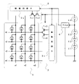
- Self-luminous display panel (light-emitting device) 2 Data driver 2a Drive circuit A 3 Scan Driver 3a Drive Circuit B 4 Voltage stabilization circuit 5 Booster circuit E1 to E4 Photoelectric element (solar cell) m1 to m3 data line (anode line) n1-n4 scanning line (cathode line)
- FIG. 1 shows the first embodiment.
- This is a passive matrix type using a light emitting display panel 1 as a light emitting device and using an organic EL element as a self light emitting element mounted on the light emitting display panel.
- the display panel is configured.
- the display panel 1 includes a plurality of data lines (hereinafter also referred to as anode lines) m1 to m3 arranged in the vertical direction and a plurality of scanning lines (hereinafter also referred to as cathode lines) n1 arranged in the horizontal direction.
- Organic EL elements indicated by diode marks are connected between the data lines and the scanning lines at the positions of the intersections with n4. As a result, the organic EL elements constituting the pixels are arranged in a matrix.
- the pixels of the organic EL elements are shown in 4 rows and 3 columns in the vertical and horizontal directions due to space limitations, but this is because a large number of elements are arranged in a matrix in the vertical and horizontal directions over the entire surface of the display panel 1. Arranged.
- Reference numeral 2 denotes a data driver for selectively supplying a drive current to the anode lines m1 to m3 of the display panel 1, and a part of the illustration is omitted, but the anode lines are selected for this.
- a pair of switching elements TS1 and TS2 for supplying a lighting driving potential or a non-lighting potential (for example, ground potential) of the EL element are connected to each other.
- the data driver 2 is equipped with a drive circuit A indicated by reference numeral 2a including a logic circuit composed of a shift register or the like that controls on / off of the switching elements TS1, TS2 corresponding to the anode line based on the image data.
- Reference numeral 3 denotes a scanning driver that selectively scans the cathode lines n1 to n4 of the display panel 1.
- each cathode line has a scanning potential (for example, ground). Potential) or a pair of switching elements TS3 and TS4 for applying a reverse bias potential are connected to each other.
- the scanning driver 3 includes a driving circuit B indicated by reference numeral 3a including a logic circuit including a shift register for controlling on / off of the switching elements TS3 and TS4 corresponding to the cathode lines based on the scanning synchronization signal of the image data. Has been.
- reference numerals E1 to E4 are photoelectric elements that supply driving power to the display panel 1 via the data driver 2 and the scanning driver 3 described above, and are constituted by serially connected bodies of solar cells. .
- a direct current output by a series connection body of solar cells shown as E1 to E4 is supplied to a voltage stabilizing circuit 4 that limits an output voltage value.
- the output from the voltage stabilization circuit 4 is configured to be supplied as drive power to the drive circuits A and B including the above-described logic circuits in the data driver 2 and the scan driver 3, respectively.
- the drive circuits A and B each including the above-described logic circuit have, for example, a 3.3V system voltage specification, and the voltage stabilization circuit 4 has a DC output generated by the solar cells E1 to E4. Is converted to a stabilized voltage value of about 3.3 V and supplied to the drive circuits A and B.
- the drive circuit A in the data driver 2 and the scan driver 3 can be controlled by the output voltage control function by the voltage stabilization circuit 4 described above.
- the voltage stabilization circuit 4 described above.
- the output voltage of the solar cells E1 to E4 is lowered and the output voltage of the voltage stabilization circuit 4 is not stably controlled (the output voltage of the voltage stabilization circuit 4 is determined by the logic circuit). It is desirable that the output from the voltage stabilization circuit 4 be stopped (shut off) in a case where the voltage value drops to such a level that the operation becomes impossible.
- the outputs from the solar cells E1 to E4 are configured not to go through the voltage stabilizing circuit 4 but to be used as a driving power source for the organic EL element. . That is, the output from the solar battery cell is supplied to one of the switching elements TS1, TS2 in the data driver 2 and the organic EL element in the scanning state via the anode line.
- the output from the solar battery cell is supplied as a reverse bias voltage to the organic EL element via any one of the switching elements TS3 and TS4 in the scanning driver 3 and a cathode line not selected for scanning. This prevents crosstalk light emission that occurs in the passive matrix display panel.
- the organic EL element as the self-luminous element has a characteristic that the light emission luminance changes according to the anode voltage. Therefore, according to the above-described configuration in which the output from the solar battery cell is used as the drive power supply, the light emission luminance of the organic EL element similarly changes according to the amount of external light received by the solar battery cell. That is, dimmer control is performed in which the overall luminance of the display panel 1 changes according to the external light.
- the display panel 1 is subjected to dimmer control according to the external light, the visibility can be improved.
- the data driver 2 and the scan driver 3 that drive the display panel 1 are assured of stable operation within a range where the output voltage value by the voltage stabilizing circuit 4 is controlled within a predetermined value. .
- FIG. 2 shows a second embodiment of the display device according to the present invention.
- parts corresponding to the parts shown in FIG. 1 already described are denoted by the same reference numerals. Therefore, the detailed description is abbreviate
- the outputs of the solar cells E1 to E4 as the photoelectric elements described above are sent to the organic EL elements arranged on the display panel 1 via the booster circuit (DC-DC converter) indicated by reference numeral 5. It is comprised so that it may be supplied as drive power.
- the booster circuit DC-DC converter
- a charge pump can be suitably used as the booster circuit 5, but a booster circuit using electromagnetic conversion means using a coil may be used depending on the equipment to be applied. it can.
- the display panel 1 can be driven to emit light even when the electromotive force generated by the solar cells E1 to E4 is insufficient. Then, by using the above-described charge pump or the like as the booster circuit 5, the display panel 1 is subjected to dimmer control according to the external light, so that the visibility can be improved. The same effect as the embodiment can be obtained.
- FIG. 3 shows a third embodiment of the display device according to the present invention.
- a part of the solar cells E1 to E4 composed of series connection bodies as photoelectric elements, that is, the output of the solar cells indicated by E1 to E3 is supplied to the voltage stabilizing circuit 4 described above.
- the voltage stabilizing circuit 4 supplies the driving circuits A and B indicated by reference numerals 2a and 3a as driving power.
- the organic EL element as the self-luminous element in the display panel 1 is configured so that the output of the solar battery cell composed of a series connection body of E1 to E4 is supplied as a driving power source.
- the voltage drop in the voltage stabilizing circuit 4 can be reduced when the rated voltage is applied to the drive circuits A and B including the logic circuit driven by a relatively low voltage.
- the utilization efficiency of the power from the cell can be increased. Also in the embodiment shown in FIG. 3, the same effects as those in the first embodiment shown in FIG. 1 can be obtained.
- FIG. 4 shows a fourth embodiment of a display device according to the present invention.
- the example shown in FIG. 4 shows an active matrix display panel 1 using an organic EL element as a self-luminous element. It is composed. Also in FIG. 4, parts corresponding to the parts shown in FIG. Therefore, the detailed description is abbreviate
- the display panel 1 in FIG. 4 shows the most basic pixel circuit constituting one pixel.
- the pixel circuits are shown in 3 rows and 2 columns due to space limitations, and a large number of pixel circuits are arranged in a matrix in the vertical and horizontal directions over the entire surface of the display panel 1.
- each pixel circuit is composed of a data writing transistor T1, a driving transistor T2, a charge holding capacitor Cs, and an organic EL element EL, as indicated by a reference numeral for one pixel circuit.
- a data signal corresponding to the video signal is supplied from the data driver 2 to the source of the data write transistor T1, and a write pulse is supplied from the scan driver 3 to the gate of the data write transistor T1. It is configured as follows.
- the drain of the data write transistor T1 is connected to the gate of the drive transistor T2 and to one terminal of the charge holding capacitor Cs.
- the source of the driving transistor T2 is connected to the other terminal of the capacitor Cs, and the outputs of the solar cells E1 to E4 are supplied as driving power.
- the drain of the driving transistor T2 is connected to the anode terminal of the organic EL element EL as a self-light-emitting element, and the cathode terminal of the organic EL element EL is connected to the reference potential point (ground) of the display panel 1. .
- the direct current output from the solar cells as photoelectric elements indicated by E1 to E4 is supplied to the data driver 2 via the voltage stabilization circuit (regulator) 4 that limits the output voltage value.
- the scanning driver 3 is configured to be supplied as drive power.
- the data driver 2 and the scan driver 3 are within the range in which the voltage is controlled within a predetermined value by the voltage stabilizing circuit 4 described above. As a result, stable operation is guaranteed.
- each pixel circuit forms a series circuit of the driving transistor T2 and the organic EL element EL as described above, the organic EL element that forms the pixel circuit according to the magnitude of external light received by the solar battery cell.
- the emission luminance of the light source changes. That is, dimmer control is performed in which the overall luminance of the display panel 1 changes according to the external light.
- an organic EL element formed by laminating thin film layers as a display panel is adopted, and driving is performed by combining the above-described solar battery cell as a photoelectric element that supplies driving power thereto.
- a lightweight and thin display device provided with a power source can be provided.
Landscapes
- Engineering & Computer Science (AREA)
- Physics & Mathematics (AREA)
- Computer Hardware Design (AREA)
- General Physics & Mathematics (AREA)
- Theoretical Computer Science (AREA)
- Electroluminescent Light Sources (AREA)
- Control Of Indicators Other Than Cathode Ray Tubes (AREA)
- Control Of El Displays (AREA)
- Photovoltaic Devices (AREA)
Abstract
Description
2 データドライバ
2a 駆動回路A
3 走査ドライバ
3a 駆動回路B
4 電圧安定化回路
5 昇圧回路
E1~E4 光電素子(太陽電池セル)
m1~m3 データ線(陽極線)
n1~n4 走査線(陰極線) 1 Self-luminous display panel (light-emitting device)
2 Data driver 2a Drive circuit A
3 Scan Driver 3a Drive Circuit B
4
m1 to m3 data line (anode line)
n1-n4 scanning line (cathode line)
Claims (10)
- 外光の照度に応じて起電力を出力する光電素子と、少なくとも1つの自発光素子が配置された発光装置と、前記発光装置を駆動制御するための駆動回路とが備えられ、
前記駆動回路に備えられた論理回路には、前記光電素子からの出力電圧値を制限する電圧安定化回路を介して論理回路への駆動電源として供給されると共に、前記自発光素子には前記電圧安定化回路を介さずに前記光電素子より自発光素子への駆動電源として供給されるように構成され、前記自発光素子は外光の照度に応じた輝度で発光されることを特徴とする表示装置。 A photoelectric element that outputs an electromotive force according to the illuminance of outside light, a light emitting device in which at least one self-light emitting element is disposed, and a drive circuit for driving and controlling the light emitting device are provided.
The logic circuit provided in the drive circuit is supplied as a drive power supply to the logic circuit via a voltage stabilization circuit that limits the output voltage value from the photoelectric element, and the self-luminous element has the voltage A display that is configured to be supplied as a driving power source from the photoelectric element to the self-light-emitting element without going through a stabilization circuit, and the self-light-emitting element emits light with a luminance according to the illuminance of external light. apparatus. - 前記光電素子の出力は、昇圧回路を介して前記自発光素子への駆動電源として供給されるように構成されていることを特徴とする請求項1に記載された表示装置。 The display device according to claim 1, wherein the output of the photoelectric element is configured to be supplied as a driving power source to the self-light-emitting element via a booster circuit.
- 前記光電素子は、それぞれが光電変換機能を果たす単位素子の直列接続体により構成され、前記直列接続体のうちの一部の単位素子による出力を、前記電圧安定化回路を介して論理回路への駆動電源として供給するように構成したことを特徴とする請求項1または請求項2に記載された表示装置。 Each of the photoelectric elements is configured by a series connection body of unit elements each performing a photoelectric conversion function, and an output from a part of the unit elements of the series connection body is output to a logic circuit via the voltage stabilization circuit. The display device according to claim 1, wherein the display device is configured to be supplied as a driving power source.
- 前記発光装置は、互いに交差する複数の陽極線及び複数の陰極線の各交点に自発光素子を備えるパッシブマトリクス型発光表示パネルであり、前記光電素子の出力は、自発光素子への駆動電源として前記パッシブマトリクス型表示パネルにおける前記陽極線に選択的に供給されるように構成されていることを特徴とする請求項1または請求項2に記載された表示装置。 The light emitting device is a passive matrix light emitting display panel including a self light emitting element at each intersection of a plurality of anode lines and a plurality of cathode lines intersecting each other, and an output of the photoelectric element is used as a driving power source to the self light emitting element. The display device according to claim 1, wherein the display device is configured to be selectively supplied to the anode line in the passive matrix display panel.
- 前記発光装置は、互いに交差する複数の陽極線及び複数の陰極線の各交点に自発光素子を備えるパッシブマトリクス型発光表示パネルであり、前記光電素子の出力は、自発光素子への駆動電源として前記パッシブマトリクス型表示パネルにおける前記陽極線に選択的に供給されるように構成されていることを特徴とする請求項3に記載された表示装置。 The light emitting device is a passive matrix light emitting display panel including a self light emitting element at each intersection of a plurality of anode lines and a plurality of cathode lines intersecting each other, and an output of the photoelectric element is used as a driving power source to the self light emitting element. The display device according to claim 3, wherein the display device is configured to be selectively supplied to the anode line in a passive matrix display panel.
- 前記光電素子の出力は、逆バイアス電源として、前記パッシブマトリクス型表示パネルにおける前記陰極線に選択的に供給されるように構成されていることを特徴とする請求項4に記載された表示装置。 The display device according to claim 4, wherein the output of the photoelectric element is configured to be selectively supplied to the cathode line in the passive matrix display panel as a reverse bias power source.
- 前記光電素子の出力は、逆バイアス電源として、前記パッシブマトリクス型表示パネルにおける前記陰極線に選択的に供給されるように構成されていることを特徴とする請求項5に記載された表示装置。 6. The display device according to claim 5, wherein the output of the photoelectric element is configured to be selectively supplied to the cathode line in the passive matrix display panel as a reverse bias power source.
- 前記発光装置は、互いに交差する複数のデータ線及び複数の走査線の各交点に、自発光素子と能動素子を含む画素を備えたアクティブマトリクス型発光表示パネルであり、前記光電素子の出力は、自発光素子への駆動電源として画素を構成する自発光素子と前記能動素子との直列回路にそれぞれ供給されるように構成されていることを特徴とする請求項1または請求項2に記載された表示装置。 The light emitting device is an active matrix light emitting display panel including a pixel including a self light emitting element and an active element at each intersection of a plurality of data lines and a plurality of scanning lines intersecting each other, and the output of the photoelectric element is 3. The device according to claim 1, wherein the drive device is configured to be supplied to a series circuit of a self-light-emitting element that constitutes a pixel and the active element as a driving power source for the self-light-emitting element. Display device.
- 前記光電素子は、太陽電池セルであることを特徴とする請求項1または請求項2に記載された表示装置。 The display device according to claim 1, wherein the photoelectric element is a solar battery cell.
- 前記光電素子は、太陽電池セルであることを特徴とする請求項4に記載された表示装置。 The display device according to claim 4, wherein the photoelectric element is a solar battery cell.
Priority Applications (5)
| Application Number | Priority Date | Filing Date | Title |
|---|---|---|---|
| CN2008801284130A CN101983401A (en) | 2008-03-31 | 2008-03-31 | Display device |
| EP08739416A EP2259249A4 (en) | 2008-03-31 | 2008-03-31 | Display device |
| US12/922,960 US20110012517A1 (en) | 2008-03-31 | 2008-03-31 | Organic electroluminescent device |
| JP2010505145A JP4991933B2 (en) | 2008-03-31 | 2008-03-31 | Organic EL device |
| PCT/JP2008/056302 WO2009122484A1 (en) | 2008-03-31 | 2008-03-31 | Display device |
Applications Claiming Priority (1)
| Application Number | Priority Date | Filing Date | Title |
|---|---|---|---|
| PCT/JP2008/056302 WO2009122484A1 (en) | 2008-03-31 | 2008-03-31 | Display device |
Publications (1)
| Publication Number | Publication Date |
|---|---|
| WO2009122484A1 true WO2009122484A1 (en) | 2009-10-08 |
Family
ID=41134905
Family Applications (1)
| Application Number | Title | Priority Date | Filing Date |
|---|---|---|---|
| PCT/JP2008/056302 WO2009122484A1 (en) | 2008-03-31 | 2008-03-31 | Display device |
Country Status (5)
| Country | Link |
|---|---|
| US (1) | US20110012517A1 (en) |
| EP (1) | EP2259249A4 (en) |
| JP (1) | JP4991933B2 (en) |
| CN (1) | CN101983401A (en) |
| WO (1) | WO2009122484A1 (en) |
Families Citing this family (3)
| Publication number | Priority date | Publication date | Assignee | Title |
|---|---|---|---|---|
| CN107065200A (en) * | 2012-12-28 | 2017-08-18 | 联想(北京)有限公司 | Electronic equipment and display methods |
| CN108364604A (en) * | 2018-04-16 | 2018-08-03 | 南方科技大学 | A kind of Micro-LED display systems |
| TWI769721B (en) * | 2020-03-13 | 2022-07-01 | 聚積科技股份有限公司 | Drive System |
Citations (6)
| Publication number | Priority date | Publication date | Assignee | Title |
|---|---|---|---|---|
| JPS6269240A (en) * | 1985-09-24 | 1987-03-30 | Hitachi Micro Comput Eng Ltd | Semiconductor integrated circuit device |
| JPH0168958U (en) | 1987-10-26 | 1989-05-08 | ||
| JPH0228153A (en) | 1988-04-15 | 1990-01-30 | Hitachi Chem Co Ltd | Carboxylic acid imide or its acid addition salt and antiarrhythmic agent |
| JPH0799453A (en) | 1993-04-09 | 1995-04-11 | Daewoo Electron Co Ltd | Method and equipment for variable length encoding using few memories |
| JPH08241055A (en) * | 1995-03-03 | 1996-09-17 | Omron Corp | Light emission device drive circuit |
| JP2004340998A (en) * | 2003-05-13 | 2004-12-02 | Optrex Corp | Portable display device |
Family Cites Families (16)
| Publication number | Priority date | Publication date | Assignee | Title |
|---|---|---|---|---|
| JPS58166578A (en) * | 1982-03-26 | 1983-10-01 | Nippon Denso Co Ltd | Information generator |
| DE4104761A1 (en) * | 1991-02-15 | 1992-08-20 | Bosch Siemens Hausgeraete | Display illuminating circuit for domestic equipment - saves power by deactivating main power stage and maintaining auxiliary sage during idle periods |
| JP3992407B2 (en) * | 1999-10-15 | 2007-10-17 | 多川 忠大 | Luminescent block |
| JP2002189449A (en) * | 2000-12-20 | 2002-07-05 | Nec Corp | Driving system for organic el display and portable terminal having the same |
| JP2003076333A (en) * | 2001-09-03 | 2003-03-14 | Nec Saitama Ltd | Method for adjusting luminance of display and driving circuit for the display applied by the method and portable electronic equipment |
| JP3854173B2 (en) * | 2002-02-27 | 2006-12-06 | 東北パイオニア株式会社 | Driving method of light emitting display panel and organic EL display device |
| US7154235B2 (en) * | 2002-09-30 | 2006-12-26 | Ritdisplay Corporation | Organic electroluminescent device having solar cells |
| JP3873149B2 (en) * | 2002-12-11 | 2007-01-24 | 株式会社日立製作所 | Display device |
| TW572302U (en) * | 2003-04-08 | 2004-01-11 | Richtek Technology Corp | Energy-saving type auto-contrast compensation device of OLED |
| US7345458B2 (en) * | 2003-07-07 | 2008-03-18 | Nippon Telegraph And Telephone Corporation | Booster that utilizes energy output from a power supply unit |
| US20050046595A1 (en) * | 2003-08-26 | 2005-03-03 | Mr.John Blyth | Solar powered sign annunciator |
| AU2003271383A1 (en) * | 2003-12-23 | 2005-07-07 | Hpm Industries Pty Ltd | A Solar Powered Light Assembly to Produce Light of Varying Colours |
| JP2006030318A (en) * | 2004-07-12 | 2006-02-02 | Sanyo Electric Co Ltd | Display device |
| JP4744914B2 (en) * | 2005-04-01 | 2011-08-10 | 三菱電機株式会社 | Liquid crystal display device and large liquid crystal display device using the same |
| TWI316217B (en) * | 2005-12-23 | 2009-10-21 | Innolux Display Corp | Display device and control method |
| FR2903224A1 (en) * | 2006-06-30 | 2008-01-04 | Thomson Licensing Sa | DISPLAY DEVICE AND USES THEREOF. |
-
2008
- 2008-03-31 CN CN2008801284130A patent/CN101983401A/en active Pending
- 2008-03-31 JP JP2010505145A patent/JP4991933B2/en active Active
- 2008-03-31 EP EP08739416A patent/EP2259249A4/en not_active Withdrawn
- 2008-03-31 WO PCT/JP2008/056302 patent/WO2009122484A1/en active Application Filing
- 2008-03-31 US US12/922,960 patent/US20110012517A1/en not_active Abandoned
Patent Citations (6)
| Publication number | Priority date | Publication date | Assignee | Title |
|---|---|---|---|---|
| JPS6269240A (en) * | 1985-09-24 | 1987-03-30 | Hitachi Micro Comput Eng Ltd | Semiconductor integrated circuit device |
| JPH0168958U (en) | 1987-10-26 | 1989-05-08 | ||
| JPH0228153A (en) | 1988-04-15 | 1990-01-30 | Hitachi Chem Co Ltd | Carboxylic acid imide or its acid addition salt and antiarrhythmic agent |
| JPH0799453A (en) | 1993-04-09 | 1995-04-11 | Daewoo Electron Co Ltd | Method and equipment for variable length encoding using few memories |
| JPH08241055A (en) * | 1995-03-03 | 1996-09-17 | Omron Corp | Light emission device drive circuit |
| JP2004340998A (en) * | 2003-05-13 | 2004-12-02 | Optrex Corp | Portable display device |
Non-Patent Citations (1)
| Title |
|---|
| See also references of EP2259249A4 * |
Also Published As
| Publication number | Publication date |
|---|---|
| JP4991933B2 (en) | 2012-08-08 |
| EP2259249A4 (en) | 2011-05-04 |
| JPWO2009122484A1 (en) | 2011-07-28 |
| CN101983401A (en) | 2011-03-02 |
| EP2259249A1 (en) | 2010-12-08 |
| US20110012517A1 (en) | 2011-01-20 |
Similar Documents
| Publication | Publication Date | Title |
|---|---|---|
| EP3327714B1 (en) | Electroluminescent display and method of sensing electrical characteristics of electroluminescent display | |
| TWI567711B (en) | Method and apparatus for supplying power to a display apparatus | |
| US9595216B2 (en) | Display apparatus and power supplying method performed by display apparatus in different power modes | |
| EP2234093B1 (en) | Organic Light Emitting Display Device | |
| EP2056282A2 (en) | Organic light emitting display and power supply method thereof | |
| EP3242286A1 (en) | Display device and driving method thereof | |
| US10692440B2 (en) | Pixel and organic light emitting display device including the same | |
| US20210358380A1 (en) | Pixel driving circuit, organic light emitting display panel and pixel driving method | |
| CN101453802B (en) | Organic electroluminescence display and driving method thereof | |
| US20050258772A1 (en) | Light emission device and power supply therefor | |
| US20080252217A1 (en) | Pixel, organic light emitting display using the same, and associated methods | |
| US10546530B2 (en) | Pixel driving circuit and display device thereof | |
| KR20170064142A (en) | Organic light emitting display panel, organic light emitting display device, image driving method, and sensing method | |
| JP4561855B2 (en) | Display device and driving method thereof | |
| JP4991933B2 (en) | Organic EL device | |
| JP4561856B2 (en) | Display device and driving method thereof | |
| CN109872693B (en) | Pixel, driving method, display panel with pixel and display device | |
| US8581896B2 (en) | Power supply for receiving different input voltages and organic light emitting display device using the same | |
| KR102470026B1 (en) | Pixel and organic light emittng display device including the pixel | |
| JP4631837B2 (en) | Active matrix light emitting device, pixel power supply switching method in active matrix light emitting device, and electronic apparatus | |
| KR20050046927A (en) | Power supply and light emitting display device using the power supply | |
| JP2012147029A (en) | Organic el device | |
| KR100648671B1 (en) | A method for setting a sequence of a power supply in a lighting emitting device | |
| KR100578840B1 (en) | A power supply in a lighting emitting device | |
| US20130010008A1 (en) | Display apparatus and method for driving the same |
Legal Events
| Date | Code | Title | Description |
|---|---|---|---|
| WWE | Wipo information: entry into national phase |
Ref document number: 200880128413.0 Country of ref document: CN |
|
| 121 | Ep: the epo has been informed by wipo that ep was designated in this application |
Ref document number: 08739416 Country of ref document: EP Kind code of ref document: A1 |
|
| ENP | Entry into the national phase |
Ref document number: 2010505145 Country of ref document: JP Kind code of ref document: A |
|
| WWE | Wipo information: entry into national phase |
Ref document number: 12922960 Country of ref document: US |
|
| WWE | Wipo information: entry into national phase |
Ref document number: 2008739416 Country of ref document: EP |
|
| NENP | Non-entry into the national phase |
Ref country code: DE |