US10692440B2 - Pixel and organic light emitting display device including the same - Google Patents
Pixel and organic light emitting display device including the same Download PDFInfo
- Publication number
- US10692440B2 US10692440B2 US16/251,781 US201916251781A US10692440B2 US 10692440 B2 US10692440 B2 US 10692440B2 US 201916251781 A US201916251781 A US 201916251781A US 10692440 B2 US10692440 B2 US 10692440B2
- Authority
- US
- United States
- Prior art keywords
- transistor
- node
- light emitting
- organic light
- electrode connected
- Prior art date
- Legal status (The legal status is an assumption and is not a legal conclusion. Google has not performed a legal analysis and makes no representation as to the accuracy of the status listed.)
- Active
Links
Images


Classifications
-
- G—PHYSICS
- G09—EDUCATION; CRYPTOGRAPHY; DISPLAY; ADVERTISING; SEALS
- G09G—ARRANGEMENTS OR CIRCUITS FOR CONTROL OF INDICATING DEVICES USING STATIC MEANS TO PRESENT VARIABLE INFORMATION
- G09G3/00—Control arrangements or circuits, of interest only in connection with visual indicators other than cathode-ray tubes
- G09G3/20—Control arrangements or circuits, of interest only in connection with visual indicators other than cathode-ray tubes for presentation of an assembly of a number of characters, e.g. a page, by composing the assembly by combination of individual elements arranged in a matrix no fixed position being assigned to or needed to be assigned to the individual characters or partial characters
- G09G3/22—Control arrangements or circuits, of interest only in connection with visual indicators other than cathode-ray tubes for presentation of an assembly of a number of characters, e.g. a page, by composing the assembly by combination of individual elements arranged in a matrix no fixed position being assigned to or needed to be assigned to the individual characters or partial characters using controlled light sources
- G09G3/30—Control arrangements or circuits, of interest only in connection with visual indicators other than cathode-ray tubes for presentation of an assembly of a number of characters, e.g. a page, by composing the assembly by combination of individual elements arranged in a matrix no fixed position being assigned to or needed to be assigned to the individual characters or partial characters using controlled light sources using electroluminescent panels
- G09G3/32—Control arrangements or circuits, of interest only in connection with visual indicators other than cathode-ray tubes for presentation of an assembly of a number of characters, e.g. a page, by composing the assembly by combination of individual elements arranged in a matrix no fixed position being assigned to or needed to be assigned to the individual characters or partial characters using controlled light sources using electroluminescent panels semiconductive, e.g. using light-emitting diodes [LED]
- G09G3/3208—Control arrangements or circuits, of interest only in connection with visual indicators other than cathode-ray tubes for presentation of an assembly of a number of characters, e.g. a page, by composing the assembly by combination of individual elements arranged in a matrix no fixed position being assigned to or needed to be assigned to the individual characters or partial characters using controlled light sources using electroluminescent panels semiconductive, e.g. using light-emitting diodes [LED] organic, e.g. using organic light-emitting diodes [OLED]
- G09G3/3225—Control arrangements or circuits, of interest only in connection with visual indicators other than cathode-ray tubes for presentation of an assembly of a number of characters, e.g. a page, by composing the assembly by combination of individual elements arranged in a matrix no fixed position being assigned to or needed to be assigned to the individual characters or partial characters using controlled light sources using electroluminescent panels semiconductive, e.g. using light-emitting diodes [LED] organic, e.g. using organic light-emitting diodes [OLED] using an active matrix
- G09G3/3233—Control arrangements or circuits, of interest only in connection with visual indicators other than cathode-ray tubes for presentation of an assembly of a number of characters, e.g. a page, by composing the assembly by combination of individual elements arranged in a matrix no fixed position being assigned to or needed to be assigned to the individual characters or partial characters using controlled light sources using electroluminescent panels semiconductive, e.g. using light-emitting diodes [LED] organic, e.g. using organic light-emitting diodes [OLED] using an active matrix with pixel circuitry controlling the current through the light-emitting element
-
- G—PHYSICS
- G09—EDUCATION; CRYPTOGRAPHY; DISPLAY; ADVERTISING; SEALS
- G09G—ARRANGEMENTS OR CIRCUITS FOR CONTROL OF INDICATING DEVICES USING STATIC MEANS TO PRESENT VARIABLE INFORMATION
- G09G3/00—Control arrangements or circuits, of interest only in connection with visual indicators other than cathode-ray tubes
- G09G3/20—Control arrangements or circuits, of interest only in connection with visual indicators other than cathode-ray tubes for presentation of an assembly of a number of characters, e.g. a page, by composing the assembly by combination of individual elements arranged in a matrix no fixed position being assigned to or needed to be assigned to the individual characters or partial characters
- G09G3/22—Control arrangements or circuits, of interest only in connection with visual indicators other than cathode-ray tubes for presentation of an assembly of a number of characters, e.g. a page, by composing the assembly by combination of individual elements arranged in a matrix no fixed position being assigned to or needed to be assigned to the individual characters or partial characters using controlled light sources
- G09G3/30—Control arrangements or circuits, of interest only in connection with visual indicators other than cathode-ray tubes for presentation of an assembly of a number of characters, e.g. a page, by composing the assembly by combination of individual elements arranged in a matrix no fixed position being assigned to or needed to be assigned to the individual characters or partial characters using controlled light sources using electroluminescent panels
- G09G3/32—Control arrangements or circuits, of interest only in connection with visual indicators other than cathode-ray tubes for presentation of an assembly of a number of characters, e.g. a page, by composing the assembly by combination of individual elements arranged in a matrix no fixed position being assigned to or needed to be assigned to the individual characters or partial characters using controlled light sources using electroluminescent panels semiconductive, e.g. using light-emitting diodes [LED]
- G09G3/3208—Control arrangements or circuits, of interest only in connection with visual indicators other than cathode-ray tubes for presentation of an assembly of a number of characters, e.g. a page, by composing the assembly by combination of individual elements arranged in a matrix no fixed position being assigned to or needed to be assigned to the individual characters or partial characters using controlled light sources using electroluminescent panels semiconductive, e.g. using light-emitting diodes [LED] organic, e.g. using organic light-emitting diodes [OLED]
- G09G3/3266—Details of drivers for scan electrodes
-
- G—PHYSICS
- G09—EDUCATION; CRYPTOGRAPHY; DISPLAY; ADVERTISING; SEALS
- G09G—ARRANGEMENTS OR CIRCUITS FOR CONTROL OF INDICATING DEVICES USING STATIC MEANS TO PRESENT VARIABLE INFORMATION
- G09G3/00—Control arrangements or circuits, of interest only in connection with visual indicators other than cathode-ray tubes
- G09G3/20—Control arrangements or circuits, of interest only in connection with visual indicators other than cathode-ray tubes for presentation of an assembly of a number of characters, e.g. a page, by composing the assembly by combination of individual elements arranged in a matrix no fixed position being assigned to or needed to be assigned to the individual characters or partial characters
- G09G3/22—Control arrangements or circuits, of interest only in connection with visual indicators other than cathode-ray tubes for presentation of an assembly of a number of characters, e.g. a page, by composing the assembly by combination of individual elements arranged in a matrix no fixed position being assigned to or needed to be assigned to the individual characters or partial characters using controlled light sources
- G09G3/30—Control arrangements or circuits, of interest only in connection with visual indicators other than cathode-ray tubes for presentation of an assembly of a number of characters, e.g. a page, by composing the assembly by combination of individual elements arranged in a matrix no fixed position being assigned to or needed to be assigned to the individual characters or partial characters using controlled light sources using electroluminescent panels
- G09G3/32—Control arrangements or circuits, of interest only in connection with visual indicators other than cathode-ray tubes for presentation of an assembly of a number of characters, e.g. a page, by composing the assembly by combination of individual elements arranged in a matrix no fixed position being assigned to or needed to be assigned to the individual characters or partial characters using controlled light sources using electroluminescent panels semiconductive, e.g. using light-emitting diodes [LED]
- G09G3/3208—Control arrangements or circuits, of interest only in connection with visual indicators other than cathode-ray tubes for presentation of an assembly of a number of characters, e.g. a page, by composing the assembly by combination of individual elements arranged in a matrix no fixed position being assigned to or needed to be assigned to the individual characters or partial characters using controlled light sources using electroluminescent panels semiconductive, e.g. using light-emitting diodes [LED] organic, e.g. using organic light-emitting diodes [OLED]
- G09G3/3275—Details of drivers for data electrodes
- G09G3/3291—Details of drivers for data electrodes in which the data driver supplies a variable data voltage for setting the current through, or the voltage across, the light-emitting elements
-
- H01L27/1225—
-
- H01L27/124—
-
- H01L27/3262—
-
- H01L27/3265—
-
- H01L27/3276—
-
- H—ELECTRICITY
- H10—SEMICONDUCTOR DEVICES; ELECTRIC SOLID-STATE DEVICES NOT OTHERWISE PROVIDED FOR
- H10D—INORGANIC ELECTRIC SEMICONDUCTOR DEVICES
- H10D86/00—Integrated devices formed in or on insulating or conducting substrates, e.g. formed in silicon-on-insulator [SOI] substrates or on stainless steel or glass substrates
- H10D86/40—Integrated devices formed in or on insulating or conducting substrates, e.g. formed in silicon-on-insulator [SOI] substrates or on stainless steel or glass substrates characterised by multiple TFTs
- H10D86/421—Integrated devices formed in or on insulating or conducting substrates, e.g. formed in silicon-on-insulator [SOI] substrates or on stainless steel or glass substrates characterised by multiple TFTs having a particular composition, shape or crystalline structure of the active layer
- H10D86/423—Integrated devices formed in or on insulating or conducting substrates, e.g. formed in silicon-on-insulator [SOI] substrates or on stainless steel or glass substrates characterised by multiple TFTs having a particular composition, shape or crystalline structure of the active layer comprising semiconductor materials not belonging to the Group IV, e.g. InGaZnO
-
- H—ELECTRICITY
- H10—SEMICONDUCTOR DEVICES; ELECTRIC SOLID-STATE DEVICES NOT OTHERWISE PROVIDED FOR
- H10D—INORGANIC ELECTRIC SEMICONDUCTOR DEVICES
- H10D86/00—Integrated devices formed in or on insulating or conducting substrates, e.g. formed in silicon-on-insulator [SOI] substrates or on stainless steel or glass substrates
- H10D86/40—Integrated devices formed in or on insulating or conducting substrates, e.g. formed in silicon-on-insulator [SOI] substrates or on stainless steel or glass substrates characterised by multiple TFTs
- H10D86/441—Interconnections, e.g. scanning lines
-
- H—ELECTRICITY
- H10—SEMICONDUCTOR DEVICES; ELECTRIC SOLID-STATE DEVICES NOT OTHERWISE PROVIDED FOR
- H10D—INORGANIC ELECTRIC SEMICONDUCTOR DEVICES
- H10D86/00—Integrated devices formed in or on insulating or conducting substrates, e.g. formed in silicon-on-insulator [SOI] substrates or on stainless steel or glass substrates
- H10D86/40—Integrated devices formed in or on insulating or conducting substrates, e.g. formed in silicon-on-insulator [SOI] substrates or on stainless steel or glass substrates characterised by multiple TFTs
- H10D86/60—Integrated devices formed in or on insulating or conducting substrates, e.g. formed in silicon-on-insulator [SOI] substrates or on stainless steel or glass substrates characterised by multiple TFTs wherein the TFTs are in active matrices
-
- H—ELECTRICITY
- H10—SEMICONDUCTOR DEVICES; ELECTRIC SOLID-STATE DEVICES NOT OTHERWISE PROVIDED FOR
- H10K—ORGANIC ELECTRIC SOLID-STATE DEVICES
- H10K59/00—Integrated devices, or assemblies of multiple devices, comprising at least one organic light-emitting element covered by group H10K50/00
- H10K59/10—OLED displays
- H10K59/12—Active-matrix OLED [AMOLED] displays
- H10K59/121—Active-matrix OLED [AMOLED] displays characterised by the geometry or disposition of pixel elements
- H10K59/1213—Active-matrix OLED [AMOLED] displays characterised by the geometry or disposition of pixel elements the pixel elements being TFTs
-
- H—ELECTRICITY
- H10—SEMICONDUCTOR DEVICES; ELECTRIC SOLID-STATE DEVICES NOT OTHERWISE PROVIDED FOR
- H10K—ORGANIC ELECTRIC SOLID-STATE DEVICES
- H10K59/00—Integrated devices, or assemblies of multiple devices, comprising at least one organic light-emitting element covered by group H10K50/00
- H10K59/10—OLED displays
- H10K59/12—Active-matrix OLED [AMOLED] displays
- H10K59/121—Active-matrix OLED [AMOLED] displays characterised by the geometry or disposition of pixel elements
- H10K59/1216—Active-matrix OLED [AMOLED] displays characterised by the geometry or disposition of pixel elements the pixel elements being capacitors
-
- H—ELECTRICITY
- H10—SEMICONDUCTOR DEVICES; ELECTRIC SOLID-STATE DEVICES NOT OTHERWISE PROVIDED FOR
- H10K—ORGANIC ELECTRIC SOLID-STATE DEVICES
- H10K59/00—Integrated devices, or assemblies of multiple devices, comprising at least one organic light-emitting element covered by group H10K50/00
- H10K59/10—OLED displays
- H10K59/12—Active-matrix OLED [AMOLED] displays
- H10K59/131—Interconnections, e.g. wiring lines or terminals
-
- H—ELECTRICITY
- H10—SEMICONDUCTOR DEVICES; ELECTRIC SOLID-STATE DEVICES NOT OTHERWISE PROVIDED FOR
- H10K—ORGANIC ELECTRIC SOLID-STATE DEVICES
- H10K59/00—Integrated devices, or assemblies of multiple devices, comprising at least one organic light-emitting element covered by group H10K50/00
- H10K59/30—Devices specially adapted for multicolour light emission
- H10K59/35—Devices specially adapted for multicolour light emission comprising red-green-blue [RGB] subpixels
-
- G—PHYSICS
- G09—EDUCATION; CRYPTOGRAPHY; DISPLAY; ADVERTISING; SEALS
- G09G—ARRANGEMENTS OR CIRCUITS FOR CONTROL OF INDICATING DEVICES USING STATIC MEANS TO PRESENT VARIABLE INFORMATION
- G09G2230/00—Details of flat display driving waveforms
-
- G—PHYSICS
- G09—EDUCATION; CRYPTOGRAPHY; DISPLAY; ADVERTISING; SEALS
- G09G—ARRANGEMENTS OR CIRCUITS FOR CONTROL OF INDICATING DEVICES USING STATIC MEANS TO PRESENT VARIABLE INFORMATION
- G09G2300/00—Aspects of the constitution of display devices
- G09G2300/04—Structural and physical details of display devices
- G09G2300/0404—Matrix technologies
- G09G2300/0408—Integration of the drivers onto the display substrate
-
- G—PHYSICS
- G09—EDUCATION; CRYPTOGRAPHY; DISPLAY; ADVERTISING; SEALS
- G09G—ARRANGEMENTS OR CIRCUITS FOR CONTROL OF INDICATING DEVICES USING STATIC MEANS TO PRESENT VARIABLE INFORMATION
- G09G2300/00—Aspects of the constitution of display devices
- G09G2300/04—Structural and physical details of display devices
- G09G2300/0421—Structural details of the set of electrodes
- G09G2300/0426—Layout of electrodes and connections
-
- G—PHYSICS
- G09—EDUCATION; CRYPTOGRAPHY; DISPLAY; ADVERTISING; SEALS
- G09G—ARRANGEMENTS OR CIRCUITS FOR CONTROL OF INDICATING DEVICES USING STATIC MEANS TO PRESENT VARIABLE INFORMATION
- G09G2300/00—Aspects of the constitution of display devices
- G09G2300/04—Structural and physical details of display devices
- G09G2300/0439—Pixel structures
-
- G—PHYSICS
- G09—EDUCATION; CRYPTOGRAPHY; DISPLAY; ADVERTISING; SEALS
- G09G—ARRANGEMENTS OR CIRCUITS FOR CONTROL OF INDICATING DEVICES USING STATIC MEANS TO PRESENT VARIABLE INFORMATION
- G09G2300/00—Aspects of the constitution of display devices
- G09G2300/08—Active matrix structure, i.e. with use of active elements, inclusive of non-linear two terminal elements, in the pixels together with light emitting or modulating elements
- G09G2300/0809—Several active elements per pixel in active matrix panels
- G09G2300/0819—Several active elements per pixel in active matrix panels used for counteracting undesired variations, e.g. feedback or autozeroing
-
- G—PHYSICS
- G09—EDUCATION; CRYPTOGRAPHY; DISPLAY; ADVERTISING; SEALS
- G09G—ARRANGEMENTS OR CIRCUITS FOR CONTROL OF INDICATING DEVICES USING STATIC MEANS TO PRESENT VARIABLE INFORMATION
- G09G2300/00—Aspects of the constitution of display devices
- G09G2300/08—Active matrix structure, i.e. with use of active elements, inclusive of non-linear two terminal elements, in the pixels together with light emitting or modulating elements
- G09G2300/0809—Several active elements per pixel in active matrix panels
- G09G2300/0842—Several active elements per pixel in active matrix panels forming a memory circuit, e.g. a dynamic memory with one capacitor
- G09G2300/0861—Several active elements per pixel in active matrix panels forming a memory circuit, e.g. a dynamic memory with one capacitor with additional control of the display period without amending the charge stored in a pixel memory, e.g. by means of additional select electrodes
-
- G—PHYSICS
- G09—EDUCATION; CRYPTOGRAPHY; DISPLAY; ADVERTISING; SEALS
- G09G—ARRANGEMENTS OR CIRCUITS FOR CONTROL OF INDICATING DEVICES USING STATIC MEANS TO PRESENT VARIABLE INFORMATION
- G09G2310/00—Command of the display device
- G09G2310/02—Addressing, scanning or driving the display screen or processing steps related thereto
- G09G2310/0262—The addressing of the pixel, in a display other than an active matrix LCD, involving the control of two or more scan electrodes or two or more data electrodes, e.g. pixel voltage dependent on signals of two data electrodes
-
- G—PHYSICS
- G09—EDUCATION; CRYPTOGRAPHY; DISPLAY; ADVERTISING; SEALS
- G09G—ARRANGEMENTS OR CIRCUITS FOR CONTROL OF INDICATING DEVICES USING STATIC MEANS TO PRESENT VARIABLE INFORMATION
- G09G2320/00—Control of display operating conditions
- G09G2320/02—Improving the quality of display appearance
- G09G2320/0209—Crosstalk reduction, i.e. to reduce direct or indirect influences of signals directed to a certain pixel of the displayed image on other pixels of said image, inclusive of influences affecting pixels in different frames or fields or sub-images which constitute a same image, e.g. left and right images of a stereoscopic display
- G09G2320/0214—Crosstalk reduction, i.e. to reduce direct or indirect influences of signals directed to a certain pixel of the displayed image on other pixels of said image, inclusive of influences affecting pixels in different frames or fields or sub-images which constitute a same image, e.g. left and right images of a stereoscopic display with crosstalk due to leakage current of pixel switch in active matrix panels
-
- G—PHYSICS
- G09—EDUCATION; CRYPTOGRAPHY; DISPLAY; ADVERTISING; SEALS
- G09G—ARRANGEMENTS OR CIRCUITS FOR CONTROL OF INDICATING DEVICES USING STATIC MEANS TO PRESENT VARIABLE INFORMATION
- G09G2320/00—Control of display operating conditions
- G09G2320/04—Maintaining the quality of display appearance
- G09G2320/043—Preventing or counteracting the effects of ageing
- G09G2320/045—Compensation of drifts in the characteristics of light emitting or modulating elements
-
- G—PHYSICS
- G09—EDUCATION; CRYPTOGRAPHY; DISPLAY; ADVERTISING; SEALS
- G09G—ARRANGEMENTS OR CIRCUITS FOR CONTROL OF INDICATING DEVICES USING STATIC MEANS TO PRESENT VARIABLE INFORMATION
- G09G2330/00—Aspects of power supply; Aspects of display protection and defect management
- G09G2330/02—Details of power systems and of start or stop of display operation
- G09G2330/021—Power management, e.g. power saving
-
- H01L29/78672—
-
- H01L29/7869—
-
- H—ELECTRICITY
- H10—SEMICONDUCTOR DEVICES; ELECTRIC SOLID-STATE DEVICES NOT OTHERWISE PROVIDED FOR
- H10D—INORGANIC ELECTRIC SEMICONDUCTOR DEVICES
- H10D30/00—Field-effect transistors [FET]
- H10D30/60—Insulated-gate field-effect transistors [IGFET]
- H10D30/67—Thin-film transistors [TFT]
- H10D30/674—Thin-film transistors [TFT] characterised by the active materials
- H10D30/6741—Group IV materials, e.g. germanium or silicon carbide
- H10D30/6743—Silicon
- H10D30/6745—Polycrystalline or microcrystalline silicon
-
- H—ELECTRICITY
- H10—SEMICONDUCTOR DEVICES; ELECTRIC SOLID-STATE DEVICES NOT OTHERWISE PROVIDED FOR
- H10D—INORGANIC ELECTRIC SEMICONDUCTOR DEVICES
- H10D30/00—Field-effect transistors [FET]
- H10D30/60—Insulated-gate field-effect transistors [IGFET]
- H10D30/67—Thin-film transistors [TFT]
- H10D30/674—Thin-film transistors [TFT] characterised by the active materials
- H10D30/6755—Oxide semiconductors, e.g. zinc oxide, copper aluminium oxide or cadmium stannate
Definitions
- Embodiments relate to a pixel and an organic light emitting device including the same.
- An organic light emitting device displays an image using an organic light emitting diode (OLED) generating light by the recombination of electrons and holes.
- OLED organic light emitting diode
- the organic light emitting device has a plurality of pixels connected to a plurality of data lines and a plurality of scan lines.
- Each pixel includes an organic light emitting diode and a driving transistor for controlling an amount of current flowing to an organic light emitting diode.
- a pixel includes: an organic light emitting diode; a first transistor including a first electrode connected to a first driving power, a second electrode connected to a first node, and a gate electrode connected to an emission control line; a second transistor connected between the first node and the second node, and having a gate electrode is connected to a third node; a third transistor connected between the second node and an anode electrode of the organic light emitting diode, and having a gate electrode connected to the emission control line; a fourth transistor connected between the first node and a data line, and having a gate electrode connected to a first scan line; a fifth transistor connected between the second node and the third node, and having a gate electrode is connected to the first scan line; a sixth transistor connected between an initializing power line and the anode electrode of the organic light emitting diode, and having a gate electrode connected to the first scan line; a seventh transistor having a first electrode connected to the initializing power line, a second electrode connected to the emission control line;
- an organic light emitting device includes: an organic light emitting display panel including a plurality of data lines, a plurality of scan lines, and a plurality of pixels; a data driving unit supplying a data voltage to the plurality of data lines to drive the plurality of data lines; a scan driving unit sequentially supplying a scan signal to the plurality of scan lines to sequentially drive the plurality of scan lines; and a control unit supplying a control signal to the data driving unit and the scan driving unit to control the data driving unit and the scan driving unit, wherein each of the plurality of pixels includes: an organic light emitting diode; a first transistor including a first electrode connected to a first driving power, a second electrode connected to a first node, and a gate electrode connected to an emission control line; a second transistor connected between the first node and the second node, and having a gate electrode connected to a third node; a third transistor connected between the second node and an anode electrode of the organic light emitting diode, and having
- FIG. 1 illustrates a drawing of an organic light emitting device according to an example embodiment
- FIG. 2 illustrates a drawing of a structure of a pixel according to an example embodiment
- FIG. 3 illustrates a waveform diagram of an example embodiment of a driving method of the pixel illustrated in FIG. 2 ;
- FIG. 4 illustrates a drawing of a structure of a pixel according to an example embodiment
- FIG. 5 illustrates a waveform diagram of an example embodiment of a driving method of the pixel illustrated in FIG. 4 .
- FIG. 1 is a drawing illustrating an organic light emitting device according to an example embodiment.
- an organic light emitting device 100 may include an organic light emitting display panel 110 , a data driving unit 120 , a scan driving unit 130 , and a control unit 140 .
- the organic light emitting display panel 110 may include a plurality of data lines DL, a plurality of scan lines SL, and a plurality of pixels P.
- the plurality of pixels P may include a circuit element, e.g., a transistor, or the like.
- each of the pixels P may include an organic light emitting diode (OLED), and a circuit element for driving the OLED, e.g., a driving transistor, or the like.
- OLED organic light emitting diode
- a structure and a driving method of a pixel according to example embodiments will be described in more detail later with reference to FIGS. 2 to 5 .
- the data driving unit 120 may supply a data voltage to the plurality of data lines DL to drive the plurality of data lines DL.
- the data driving unit 120 may include at least one source driver integrated circuit (SDIC) to drive the plurality of data lines DL.
- SDIC source driver integrated circuit
- the scan driving unit 130 may sequentially supply a scan signal to the plurality of scan lines SL to sequentially drive the plurality of scan lines SL.
- the scan driving unit 130 may include at least one gate driver integrated circuit (GDIC), e.g., a Gate In Panel (GIP) type, and may be disposed in the organic light emitting display panel 110 .
- GDIC gate driver integrated circuit
- the GIP may be implemented using a low temperature polycrystalline silicon (LTPS), and may thus have high electron mobility and fast driving characteristics.
- the control unit 140 may supply a control signal to the data driving unit 120 and the scan driving unit 130 , to control the data driving unit 120 and the scan driving unit 130 .
- the control unit 140 may receive various timing signals including, e.g., a vertical synchronizing signal (Vsync), a horizontal synchronizing signal (Hsync), an input data enable (DE) signal, a clock signal (CLK), and the like, with image data, from an external source (e.g., a host system).
- Vsync vertical synchronizing signal
- Hsync horizontal synchronizing signal
- DE input data enable
- CLK clock signal
- control unit 140 may generate a data driving control signal DCS and a scan driving control signal SCS in response to the timing signals which are received, may supply the data driving control signal DCS to the data driving unit 120 , and may supply the scan driving control signal SCS to the scan driving unit 130 .
- control unit 140 may rearrange image data Data, supplied from an external source, to supply the image data Data to the data driving unit 120 .
- the scan driving unit 130 may sequentially supply a scan signal of an On voltage or an Off voltage to the plurality of scan lines SL, according to control of the control unit 140 .
- the data driving unit 120 may convert the image data, received from the control unit 140 , into a data voltage in analog form, and may supply the data voltage to the plurality of data lines DL, when an arbitrary scan line is driven by the scan driving unit 130 .
- the data driving unit 120 is illustrated as being located on one side (e.g., an upper side or a lower side) of the organic light emitting display panel 110 .
- the data driving unit 120 may be located on each of both sides (e.g., an upper side and a lower side) of the organic light emitting display panel 110 .
- the scan driving unit 130 is illustrated as being located on one side (e.g., a left side or a right side) of the organic light emitting display panel 110 .
- the scan driving unit 130 may be located on each of both sides (e.g. a left side and a right side) of the organic light emitting display panel 110 .
- FIG. 2 is a drawing illustrating a structure of a pixel according to an example embodiment.
- a pixel according to an example embodiment may include an organic light emitting diode (OLED) and a pixel circuit 20 .
- OLED organic light emitting diode
- An anode electrode of the organic light emitting diode (OLED) is connected to the pixel circuit 20 , and may generate light having a predetermined brightness corresponding to an amount of current supplied from the pixel circuit 20 .
- the pixel circuit 20 may control an amount of current flowing from a first driving power ELVDD via an organic light emitting diode (OLED) to a second driving power ELVSS in response to a data signal Data.
- the pixel circuit 20 may include a first transistor M 1 (O) to a seventh transistor M 7 (O) and a storage capacitor Cst.
- the first transistor M 1 (O) may have a first electrode connected to the first driving power ELVDD, a second electrode connected to a first node N 1 , and a gate electrode connected to an emission control line. Thus, the first transistor M 1 (O) may be turned-off when an emission control signal EM(n) is supplied and turned-on when the emission control signal EM(n) is not supplied.
- a second transistor M 2 is connected between a first node N 1 and a second node N 2 .
- a gate electrode of the second transistor M 2 is connected to a third node N 3 .
- a third transistor M 3 (O) is connected between the second node N 2 and an anode electrode of the organic light emitting diode (OLED).
- a gate electrode of the third transistor M 3 (O) is connected to an emission control line to be turned-off when an emission control signal EM(n) is supplied and to be turned-on when the emission control signal EM(n) is not supplied.
- a fourth transistor M 4 (O) is connected between the first node N 1 and a data line.
- a gate electrode of the fourth transistor M 4 (O) is connected to a first scan line to be turned-on when a first scan signal Oxide(n) is supplied.
- the fourth transistor M 4 (O) is turned-on, the data line and the first node N 1 are electrically connected to each other.
- a fifth transistor M 5 (O) is connected between the second node N 2 and a third node N 3 .
- a gate electrode of the fifth transistor M 5 (O) is connected to a first scan line to be turned-on when a first scan signal Oxide(n) is supplied.
- the fifth transistor M 5 (O) is turned-on, the second node N 2 and the third node N 3 are electrically connected to each other.
- a sixth transistor M 6 (O) is connected between an initializing power line to which an initializing power Vint is supplied and an anode electrode of the organic light emitting diode (OLED).
- a gate electrode of the sixth transistor M 6 (O) is connected to a first scan line to be turned-on when a first scan signal Oxide(n) is supplied.
- the initializing power Vint is supplied to the anode electrode of the organic light emitting diode (OLED).
- the seventh transistor M 7 (O) has a first electrode connected to the initializing power line, a second electrode connected to the third node N 3 , and a gate electrode connected to a second scan line to be turned-on when a second scan signal Oxide(n ⁇ 1) is supplied.
- the initializing power Vint is supplied to the gate electrode of the second transistor M 2 .
- the storage capacitor Cst is connected between the first driving power ELVDD and the third node N 3 .
- the first transistor M 1 (O) and the third transistor M 3 (O) to the seventh transistor M 7 (O), described above, may be provided as a P-type or N-type oxide semiconductor thin film transistor.
- the first transistor M 1 (O) and the third transistor M 3 (O) to the seventh transistor M 7 (O) are provided as an oxide semiconductor thin film transistor, voltage fluctuations caused by a leakage current may be significantly reduced, so driving may be performed at a low scanning rate.
- the second transistor M 2 described above may be provided as a P-type or N-type LTPS thin film transistor.
- an organic light emitting device may output a high brightness with reduced power consumption by setting a driving voltage to be low or by using a low scanning rate.
- a thin film transistor made of low temperature polycrystalline silicon (LTPS)
- LTPS low temperature polycrystalline silicon
- oxide semiconductor thin film transistors by using oxide semiconductor thin film transistors, the driving at a low scanning rate may be realized with a significantly reduced leakage current.
- a driving unit for driving each of the oxide semiconductor thin film transistor and the LTPS thin film transistor is not required to be separately provided, so a structure of a shift register for realizing a driving unit may be simplified. For example, in addition to the scan signals Oxide(n) described above, a separate scan signal Scan(n) would be needed for driving the LTPS thin film transistor(s).
- an oxide semiconductor thin film transistor for transistors to be controlled by an emission control signal EM(n) and for the driving transistor, a driving unit for driving each of an oxide semiconductor thin film transistor and an LTPS thin film transistor is not required to be separately provided, so a structure of a shift register for implementing a driving unit may be simplified.
- FIG. 3 is a waveform diagram illustrating an example embodiment of a driving method of the pixel illustrated in FIG. 2 .
- a first transistor M 1 (O) and a third transistor M 3 (O) are turned-off.
- the first transistor M 1 (O) is turned-off, an electrical connection between the first driving power ELVDD and the first node N 1 is blocked.
- the third transistor M 3 (O) is turned-off, an electrical connection between the second node N 2 and an organic light emitting diode (OLED) is blocked.
- the fifth transistor M 5 (O) When the fifth transistor M 5 (O) is turned-on, the second node N 2 and the third node N 3 are electrically connected to each other, so the second transistor M 2 is connected in a diode form.
- the third node N 3 is initialized to initializing power Vint, lower than the data signal Data
- the second transistor M 2 since the third node N 3 is initialized to initializing power Vint, lower than the data signal Data, the second transistor M 2 is turned-on, so the data signal Data, supplied to the first node N 1 , is supplied to the third node N 3 via the second transistor M 2 .
- the storage capacitor Cst may store a voltage applied to the third node N 3 .
- the initializing power Vint is supplied to the anode electrode of the organic light emitting diode (OLED).
- the first transistor M 1 (O) and the third transistor M 3 (O) are turned-on.
- the first driving power ELVDD and the first node N 1 are electrically connected to each other.
- the third transistor M 3 (O) is turned-on, the second transistor M 2 and an organic light emitting diode (OLED) are electrically connected to each other.
- the second transistor M 2 controls an amount of current flowing from the first driving power ELVDD via the organic light emitting diode (OLED) to the second driving power ELVSS in response to a voltage of the third node N 3 .
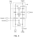
- FIG. 4 is a drawing illustrating a structure of a pixel according to an example embodiment.
- a pixel according to an example embodiment may include an organic light emitting diode (OLED) and a pixel circuit 40 .
- the pixel circuit 40 illustrated in FIG. 4 has the same configuration as that of FIG. 2 , but the LTPS thin film transistor M 2 is replaced by an oxide semiconductor thin film transistors M 2 (O), such that all transistors M 1 (O) to M 7 (O) are oxide semiconductor thin film transistors.
- An anode electrode of the organic light emitting diode (OLED) is connected to the pixel circuit 40 , and may generate light having a predetermined brightness, corresponding to an amount of current supplied from the pixel circuit 40 .
- the pixel circuit 40 may control an amount of current flowing from a first driving power ELVDD via an organic light emitting diode (OLED) to a second driving power ELVSS in response to a data signal Data.
- the pixel circuit 40 may include the first transistor M 1 (O) to the seventh transistor M 7 (O) and a storage capacitor Cst.
- the first transistor M 1 (O) may have a first electrode connected to the first driving power ELVDD, a second electrode is connected to a first node N 1 , and a gate electrode of the first transistor M 1 (O) connected to an emission control line.
- the first transistor M 1 (O) to be turned-off when an emission control signal EM(n) is supplied and to be turned-on when the emission control signal EM(n) is not supplied.
- the second transistor M 2 (O) is connected between a first node N 1 and a second node N 2 .
- a gate electrode of the second transistor M 2 (O) is connected to a third node N 3 .
- the third transistor M 3 (O) is connected between the second node N 2 and an anode electrode of the organic light emitting diode (OLED).
- a gate electrode of the third transistor M 3 (O) is connected to an emission control line to be turned-off when an emission control signal EM(n) is supplied, and to be turned-on when the emission control signal EM(n) is not supplied.
- the fourth transistor M 4 (O) is connected between the first node N 1 and a data line.
- a gate electrode of the fourth transistor M 4 (O) is connected to a first scan line to be turned-on when a first scan signal Oxide(n) is supplied.
- the fourth transistor M 4 (O) is turned-on, the data line and the first node N 1 are electrically connected to each other.
- the fifth transistor M 5 (O) is connected between the second node N 2 and a third node N 3 .
- a gate electrode of the fifth transistor M 5 (O) is connected to a first scan line to be turned-on when a first scan signal Oxide(n) is supplied.
- the fifth transistor M 5 (O) is turned-on, the second node N 2 and the third node N 3 are electrically connected to each other.
- the sixth transistor M 6 (O) is connected between an initializing power line to which an initializing power Vint is supplied and an anode electrode of the organic light emitting diode (OLED).
- a gate electrode of the sixth transistor M 6 (O) is connected to a first scan line to be turned-on when a first scan signal Oxide(n) is supplied.
- the initializing power Vint is supplied to the anode electrode of the organic light emitting diode (OLED).
- the seventh transistor M 7 (O) may include a first electrode connected to the initializing power line, a second electrode connected to the third node N 3 .
- a gate electrode of the seventh transistor M 7 (O) is connected to a second scan line to be turned-on when a second scan signal Oxide(n ⁇ 1) is supplied.
- the initializing power Vint is supplied to the gate electrode of the second transistor M 2 .
- the storage capacitor Cst is connected between the first driving power ELVDD and the third node N 3 .
- the first transistor M 1 (O) to the seventh transistor M 7 (O), described above, may be provided as a P-type or N-type oxide semiconductor thin film transistor. As described above, when the first transistor M 1 (O) to the seventh transistor M 7 (O) are provided as an oxide semiconductor thin film transistor, voltage fluctuations caused by a leakage current may be significantly reduced, so driving may be performed at a low scanning rate.
- a driving unit for driving each of the oxide semiconductor thin film transistor and the LTPS thin film transistor is not required to be separately provided, so a structure of a shift register for realizing a driving unit may be simplified.
- FIG. 5 is a waveform diagram illustrating an example embodiment of a driving method of the pixel illustrated in FIG. 4 .
- the waveform diagram of FIG. 5 is the same as that of FIG. 3 .
- a first transistor M 1 (O) and a third transistor M 3 (O) are turned-off.
- the first transistor M 1 (O) is turned-off, an electrical connection between the first driving power ELVDD and the first node N 1 is blocked.
- the third transistor M 3 (O) is turned-off, an electrical connection between the second node N 2 and an organic light emitting diode (OLED) is blocked.
- the fifth transistor M 5 (O) When the fifth transistor M 5 (O) is turned-on, the second node N 2 and the third node N 3 are electrically connected to each other, so the second transistor M 2 (O) is connected in a diode form.
- the third node N 3 is initialized to initializing power Vint, lower than the data signal Data
- the second transistor M 2 (O) since the third node N 3 is initialized to initializing power Vint, lower than the data signal Data, the second transistor M 2 (O) is turned-on, so the data signal Data, supplied to the first node N 1 , is supplied via the second transistor M 2 (O) to the third node N 3 .
- the storage capacitor Cst may store a voltage applied to the third node N 3 .
- the initializing power Vint is supplied to the anode electrode of the organic light emitting diode (OLED).
- the first transistor M 1 (O) and the third transistor M 3 (O) are turned-on.
- the first driving power ELVDD and the first node N 1 are electrically connected to each other.
- the third transistor M 3 (O) is turned-on, the second transistor M 2 (O) and an organic light emitting diode (OLED) are electrically connected to each other.
- the second transistor M 2 (O) controls an amount of current flowing from the first driving power ELVDD via the organic light emitting diode (OLED) to the second driving power ELVSS in response to a voltage of the third node N 3 .
- a pixel capable of significantly reducing power consumption with a simplified driving unit and an organic light emitting device including the same are provided.
Landscapes
- Engineering & Computer Science (AREA)
- Physics & Mathematics (AREA)
- Computer Hardware Design (AREA)
- General Physics & Mathematics (AREA)
- Theoretical Computer Science (AREA)
- Microelectronics & Electronic Packaging (AREA)
- Geometry (AREA)
- Electroluminescent Light Sources (AREA)
- Control Of El Displays (AREA)
- Control Of Indicators Other Than Cathode Ray Tubes (AREA)
Abstract
Description
Claims (10)
Applications Claiming Priority (2)
| Application Number | Priority Date | Filing Date | Title |
|---|---|---|---|
| KR10-2018-0071086 | 2018-06-20 | ||
| KR1020180071086A KR102514242B1 (en) | 2018-06-20 | 2018-06-20 | Pixel and organic light emitting display device comprising the same |
Publications (2)
| Publication Number | Publication Date |
|---|---|
| US20190392765A1 US20190392765A1 (en) | 2019-12-26 |
| US10692440B2 true US10692440B2 (en) | 2020-06-23 |
Family
ID=68968398
Family Applications (1)
| Application Number | Title | Priority Date | Filing Date |
|---|---|---|---|
| US16/251,781 Active US10692440B2 (en) | 2018-06-20 | 2019-01-18 | Pixel and organic light emitting display device including the same |
Country Status (3)
| Country | Link |
|---|---|
| US (1) | US10692440B2 (en) |
| KR (1) | KR102514242B1 (en) |
| CN (1) | CN110634446B (en) |
Cited By (2)
| Publication number | Priority date | Publication date | Assignee | Title |
|---|---|---|---|---|
| US11410604B2 (en) | 2020-03-31 | 2022-08-09 | Chengdu Boe Optoelectronics Technology Co., Ltd. | Pixel circuit and a method of driving the same and a display panel |
| US12462750B2 (en) | 2022-11-14 | 2025-11-04 | Wuhan China Star Optoelectronics Semiconductor Display Technology Co., Ltd. | Pixel circuit and display panel |
Families Citing this family (8)
| Publication number | Priority date | Publication date | Assignee | Title |
|---|---|---|---|---|
| US11341878B2 (en) | 2019-03-21 | 2022-05-24 | Samsung Display Co., Ltd. | Display panel and method of testing display panel |
| CN111968577B (en) * | 2020-08-27 | 2022-01-11 | 云谷(固安)科技有限公司 | Display panel and display device |
| CN114333667B (en) * | 2020-09-30 | 2024-01-23 | 京东方科技集团股份有限公司 | Gate driving circuit and driving method thereof and display panel |
| CN112233616A (en) * | 2020-10-12 | 2021-01-15 | Oppo广东移动通信有限公司 | Pixel driving circuit, display device and driving method |
| CN112669776B (en) * | 2021-01-22 | 2023-02-03 | 昆山国显光电有限公司 | Pixel circuit, driving method thereof and display panel |
| CN113112964B (en) * | 2021-04-14 | 2022-08-09 | 京东方科技集团股份有限公司 | Pixel circuit, pixel driving method and display device |
| KR102641231B1 (en) * | 2021-10-06 | 2024-02-29 | 호서대학교 산학협력단 | Scan driver |
| CN118251056A (en) | 2021-12-23 | 2024-06-25 | 京东方科技集团股份有限公司 | Display substrate and driving method thereof, and display device |
Citations (16)
| Publication number | Priority date | Publication date | Assignee | Title |
|---|---|---|---|---|
| US20120001893A1 (en) * | 2010-06-30 | 2012-01-05 | Samsung Mobile Display Co., Ltd. | Pixel and organic light emitting display device using the same |
| US20120162177A1 (en) | 2010-12-23 | 2012-06-28 | Samsung Mobile Display Co., Ltd. | Pixel and organic light emitting display device using the same |
| US20120235965A1 (en) | 2011-03-17 | 2012-09-20 | Au Optronics Corp. | Liquid crystal display device free of upper substrate electrode and driving method thereof |
| US8477085B2 (en) | 2006-12-15 | 2013-07-02 | Semiconductor Energy Laboratory Co., Ltd. | Semiconductor device and driving method thereof |
| US20130222356A1 (en) * | 2012-02-28 | 2013-08-29 | Jin-Tae Jeong | Pixel and organic light emitting display using the same |
| US20150055047A1 (en) | 2013-08-26 | 2015-02-26 | Apple Inc. | Liquid Crystal Displays with Oxide-Based Thin-Film Transistors |
| WO2015031037A1 (en) | 2013-08-26 | 2015-03-05 | Apple Inc. | Displays with silicon and semiconducting oxide thin-film transistors |
| US20150243220A1 (en) | 2014-02-25 | 2015-08-27 | Lg Display Co., Ltd. | Display Backplane and Method of Fabricating the Same |
| US20150364089A1 (en) | 2014-06-11 | 2015-12-17 | Samsung Display Co., Ltd. | Organic light-emitting diode (oled) display and method of setting initialization voltage in the same |
| US20160035812A1 (en) | 2014-07-31 | 2016-02-04 | Lg Display Co., Ltd. | Flexible display device with wire having reinforced portion and manufacturing method for the same |
| US9276050B2 (en) | 2014-02-25 | 2016-03-01 | Lg Display Co., Ltd. | Organic light emitting display device |
| US20160063921A1 (en) | 2014-08-26 | 2016-03-03 | Apple Inc. | Organic Light-Emitting Diode Display With Reduced Capacitive Sensitivity |
| US20160210898A1 (en) | 2013-09-04 | 2016-07-21 | Joled Inc. | Display device and driving method |
| US9634038B2 (en) | 2014-02-25 | 2017-04-25 | Lg Display Co., Ltd. | Display backplane having multiple types of thin-film-transistors |
| US20170186782A1 (en) | 2015-12-24 | 2017-06-29 | Innolux Corporation | Pixel circuit of active-matrix light-emitting diode and display panel having the same |
| US20180006099A1 (en) | 2016-07-01 | 2018-01-04 | Samsung Display Co., Ltd. | Pixel, stage circuit and organic light emitting display device having the pixel and the stage circuit |
Family Cites Families (10)
| Publication number | Priority date | Publication date | Assignee | Title |
|---|---|---|---|---|
| JP5939135B2 (en) * | 2012-07-31 | 2016-06-22 | ソニー株式会社 | Display device, driving circuit, driving method, and electronic apparatus |
| KR102061108B1 (en) * | 2013-01-16 | 2020-01-02 | 삼성디스플레이 주식회사 | Organic Light Emitting Display integrated Touch Screen Panel |
| CN104715714B (en) * | 2013-12-17 | 2017-08-04 | 昆山国显光电有限公司 | Image element circuit and its driving method and a kind of active array organic light emitting display device |
| KR102470504B1 (en) * | 2015-08-12 | 2022-11-28 | 삼성디스플레이 주식회사 | Pixel and organic light emitting display device using the same |
| KR102615740B1 (en) * | 2016-06-08 | 2023-12-19 | 삼성디스플레이 주식회사 | Display device |
| KR102607897B1 (en) * | 2016-11-18 | 2023-11-29 | 삼성디스플레이 주식회사 | Organic light emitting diode display |
| CN106531076B (en) * | 2017-01-12 | 2019-03-01 | 京东方科技集团股份有限公司 | A pixel circuit, a display panel and a driving method thereof |
| CN106710522A (en) * | 2017-02-24 | 2017-05-24 | 深圳市华星光电技术有限公司 | OLED pixel drive circuit and pixel drive method |
| CN207425322U (en) | 2017-08-30 | 2018-05-29 | 京东方科技集团股份有限公司 | Pixel circuit, display base plate and display device |
| CN107657921B (en) * | 2017-11-17 | 2019-09-24 | 深圳市华星光电半导体显示技术有限公司 | AMOLED pixel-driving circuit and its driving method |
-
2018
- 2018-06-20 KR KR1020180071086A patent/KR102514242B1/en active Active
-
2019
- 2019-01-18 US US16/251,781 patent/US10692440B2/en active Active
- 2019-06-11 CN CN201910513118.7A patent/CN110634446B/en active Active
Patent Citations (24)
| Publication number | Priority date | Publication date | Assignee | Title |
|---|---|---|---|---|
| US8477085B2 (en) | 2006-12-15 | 2013-07-02 | Semiconductor Energy Laboratory Co., Ltd. | Semiconductor device and driving method thereof |
| US20120001893A1 (en) * | 2010-06-30 | 2012-01-05 | Samsung Mobile Display Co., Ltd. | Pixel and organic light emitting display device using the same |
| US20120162177A1 (en) | 2010-12-23 | 2012-06-28 | Samsung Mobile Display Co., Ltd. | Pixel and organic light emitting display device using the same |
| US20120235965A1 (en) | 2011-03-17 | 2012-09-20 | Au Optronics Corp. | Liquid crystal display device free of upper substrate electrode and driving method thereof |
| US20130222356A1 (en) * | 2012-02-28 | 2013-08-29 | Jin-Tae Jeong | Pixel and organic light emitting display using the same |
| KR20160018825A (en) | 2013-08-26 | 2016-02-17 | 애플 인크. | Displays with silicon and semiconducting oxide thin-film transistors |
| US9129927B2 (en) | 2013-08-26 | 2015-09-08 | Apple Inc. | Organic light-emitting diode displays with semiconducting-oxide and silicon thin-film transistors |
| WO2015031037A1 (en) | 2013-08-26 | 2015-03-05 | Apple Inc. | Displays with silicon and semiconducting oxide thin-film transistors |
| US9818765B2 (en) | 2013-08-26 | 2017-11-14 | Apple Inc. | Displays with silicon and semiconducting oxide thin-film transistors |
| US20150055047A1 (en) | 2013-08-26 | 2015-02-26 | Apple Inc. | Liquid Crystal Displays with Oxide-Based Thin-Film Transistors |
| US9412799B2 (en) | 2013-08-26 | 2016-08-09 | Apple Inc. | Display driver circuitry for liquid crystal displays with semiconducting-oxide thin-film transistors |
| US9564478B2 (en) | 2013-08-26 | 2017-02-07 | Apple Inc. | Liquid crystal displays with oxide-based thin-film transistors |
| US20160210898A1 (en) | 2013-09-04 | 2016-07-21 | Joled Inc. | Display device and driving method |
| US9627462B2 (en) | 2014-02-25 | 2017-04-18 | Lg Display Co., Ltd. | Organic light emitting display device |
| US20150243220A1 (en) | 2014-02-25 | 2015-08-27 | Lg Display Co., Ltd. | Display Backplane and Method of Fabricating the Same |
| KR20150100516A (en) | 2014-02-25 | 2015-09-02 | 엘지디스플레이 주식회사 | Display backplane and method of fabricating the same |
| US9276050B2 (en) | 2014-02-25 | 2016-03-01 | Lg Display Co., Ltd. | Organic light emitting display device |
| US9634038B2 (en) | 2014-02-25 | 2017-04-25 | Lg Display Co., Ltd. | Display backplane having multiple types of thin-film-transistors |
| US20150364089A1 (en) | 2014-06-11 | 2015-12-17 | Samsung Display Co., Ltd. | Organic light-emitting diode (oled) display and method of setting initialization voltage in the same |
| US20160035812A1 (en) | 2014-07-31 | 2016-02-04 | Lg Display Co., Ltd. | Flexible display device with wire having reinforced portion and manufacturing method for the same |
| US20160063921A1 (en) | 2014-08-26 | 2016-03-03 | Apple Inc. | Organic Light-Emitting Diode Display With Reduced Capacitive Sensitivity |
| US20170186782A1 (en) | 2015-12-24 | 2017-06-29 | Innolux Corporation | Pixel circuit of active-matrix light-emitting diode and display panel having the same |
| US20180006099A1 (en) | 2016-07-01 | 2018-01-04 | Samsung Display Co., Ltd. | Pixel, stage circuit and organic light emitting display device having the pixel and the stage circuit |
| KR20180004369A (en) | 2016-07-01 | 2018-01-11 | 삼성디스플레이 주식회사 | Pixel and stage circuit and organic light emitting display device having the pixel and the stage circuit |
Non-Patent Citations (1)
| Title |
|---|
| USPTO Office action dated Mar. 20, 2020 for copending U.S. Appl. No. 16/243,609. |
Cited By (2)
| Publication number | Priority date | Publication date | Assignee | Title |
|---|---|---|---|---|
| US11410604B2 (en) | 2020-03-31 | 2022-08-09 | Chengdu Boe Optoelectronics Technology Co., Ltd. | Pixel circuit and a method of driving the same and a display panel |
| US12462750B2 (en) | 2022-11-14 | 2025-11-04 | Wuhan China Star Optoelectronics Semiconductor Display Technology Co., Ltd. | Pixel circuit and display panel |
Also Published As
| Publication number | Publication date |
|---|---|
| US20190392765A1 (en) | 2019-12-26 |
| CN110634446B (en) | 2023-02-17 |
| KR102514242B1 (en) | 2023-03-28 |
| KR20190143308A (en) | 2019-12-30 |
| CN110634446A (en) | 2019-12-31 |
Similar Documents
| Publication | Publication Date | Title |
|---|---|---|
| US11688342B2 (en) | Pixel and organic light emitting display device having the pixel | |
| KR102818266B1 (en) | Pixel and stage circuit and organic light emitting display device having the pixel and the stage circuit | |
| US10692440B2 (en) | Pixel and organic light emitting display device including the same | |
| KR102876204B1 (en) | Organic light emitting display apparatus | |
| US11450280B2 (en) | Organic light emitting display device | |
| US10700146B2 (en) | Pixel and organic light-emitting display device having the same | |
| CN110021264B (en) | Pixel circuit, driving method thereof and display panel | |
| CN109872692B (en) | Pixel circuit, driving method thereof and display device | |
| US9564083B2 (en) | Organic light emitting display device having a wiring connecting a first pixel with a second pixel | |
| US10366651B2 (en) | Organic light-emitting display device and driving method thereof | |
| US8378933B2 (en) | Pixel and organic light emitting display device using the same | |
| US20180074569A1 (en) | Display apparatus | |
| CN113129838B (en) | Gate drive circuit and display device using the same | |
| KR102943879B1 (en) | Gate driving circuit and electroluminescence display device using the same | |
| KR102583838B1 (en) | Pixel and Organic Light Emitting Display Device Using the same | |
| US10074312B2 (en) | Display device including two scan lines for same pixel | |
| CN108172171B (en) | Pixel driving circuit and organic light emitting diode display | |
| US9269296B2 (en) | Pixel and organic light emitting display device using the same | |
| KR102645963B1 (en) | Sub-pixel, gate driver and organic light emitting display device | |
| KR20250132158A (en) | Display device |
Legal Events
| Date | Code | Title | Description |
|---|---|---|---|
| AS | Assignment |
Owner name: SAMSUNG ELECTRONICS CO., LTD., KOREA, REPUBLIC OF Free format text: ASSIGNMENT OF ASSIGNORS INTEREST;ASSIGNORS:KUK, SEUNG HEE;KIM, SI WOO;KIM, WON SEOK;AND OTHERS;SIGNING DATES FROM 20181126 TO 20181128;REEL/FRAME:048060/0001 |
|
| FEPP | Fee payment procedure |
Free format text: ENTITY STATUS SET TO UNDISCOUNTED (ORIGINAL EVENT CODE: BIG.); ENTITY STATUS OF PATENT OWNER: LARGE ENTITY |
|
| AS | Assignment |
Owner name: SAMSUNG ELECTRONICS CO., LTD., KOREA, REPUBLIC OF Free format text: CORRECTIVE ASSIGNMENT TO CORRECT THE TITLE OF THE INVENTION ON THE RECORDED ASSIGNMENT PREVIOUSLY RECORDED AT REEL: 048060 FRAME: 0001. ASSIGNOR(S) HEREBY CONFIRMS THE ASSIGNMENT;ASSIGNORS:KUK, SEUNG HEE;KIM, SI WOO;KIM, WON SEOK;AND OTHERS;SIGNING DATES FROM 20181126 TO 20181128;REEL/FRAME:048498/0572 |
|
| STPP | Information on status: patent application and granting procedure in general |
Free format text: NOTICE OF ALLOWANCE MAILED -- APPLICATION RECEIVED IN OFFICE OF PUBLICATIONS |
|
| STPP | Information on status: patent application and granting procedure in general |
Free format text: NOTICE OF ALLOWANCE MAILED -- APPLICATION RECEIVED IN OFFICE OF PUBLICATIONS |
|
| STPP | Information on status: patent application and granting procedure in general |
Free format text: PUBLICATIONS -- ISSUE FEE PAYMENT VERIFIED |
|
| STCF | Information on status: patent grant |
Free format text: PATENTED CASE |
|
| MAFP | Maintenance fee payment |
Free format text: PAYMENT OF MAINTENANCE FEE, 4TH YEAR, LARGE ENTITY (ORIGINAL EVENT CODE: M1551); ENTITY STATUS OF PATENT OWNER: LARGE ENTITY Year of fee payment: 4 |