WO2009107705A1 - Imaging device, and imaging element - Google Patents
Imaging device, and imaging element Download PDFInfo
- Publication number
- WO2009107705A1 WO2009107705A1 PCT/JP2009/053517 JP2009053517W WO2009107705A1 WO 2009107705 A1 WO2009107705 A1 WO 2009107705A1 JP 2009053517 W JP2009053517 W JP 2009053517W WO 2009107705 A1 WO2009107705 A1 WO 2009107705A1
- Authority
- WO
- WIPO (PCT)
- Prior art keywords
- pixel
- exit pupil
- light
- partial region
- image
- Prior art date
Links
Images


Classifications
-
- G—PHYSICS
- G02—OPTICS
- G02B—OPTICAL ELEMENTS, SYSTEMS OR APPARATUS
- G02B7/00—Mountings, adjusting means, or light-tight connections, for optical elements
- G02B7/28—Systems for automatic generation of focusing signals
-
- G—PHYSICS
- G02—OPTICS
- G02B—OPTICAL ELEMENTS, SYSTEMS OR APPARATUS
- G02B7/00—Mountings, adjusting means, or light-tight connections, for optical elements
- G02B7/28—Systems for automatic generation of focusing signals
- G02B7/34—Systems for automatic generation of focusing signals using different areas in a pupil plane
-
- G—PHYSICS
- G03—PHOTOGRAPHY; CINEMATOGRAPHY; ANALOGOUS TECHNIQUES USING WAVES OTHER THAN OPTICAL WAVES; ELECTROGRAPHY; HOLOGRAPHY
- G03B—APPARATUS OR ARRANGEMENTS FOR TAKING PHOTOGRAPHS OR FOR PROJECTING OR VIEWING THEM; APPARATUS OR ARRANGEMENTS EMPLOYING ANALOGOUS TECHNIQUES USING WAVES OTHER THAN OPTICAL WAVES; ACCESSORIES THEREFOR
- G03B13/00—Viewfinders; Focusing aids for cameras; Means for focusing for cameras; Autofocus systems for cameras
- G03B13/32—Means for focusing
- G03B13/34—Power focusing
- G03B13/36—Autofocus systems
-
- H—ELECTRICITY
- H04—ELECTRIC COMMUNICATION TECHNIQUE
- H04N—PICTORIAL COMMUNICATION, e.g. TELEVISION
- H04N23/00—Cameras or camera modules comprising electronic image sensors; Control thereof
- H04N23/60—Control of cameras or camera modules
- H04N23/67—Focus control based on electronic image sensor signals
- H04N23/672—Focus control based on electronic image sensor signals based on the phase difference signals
-
- H—ELECTRICITY
- H04—ELECTRIC COMMUNICATION TECHNIQUE
- H04N—PICTORIAL COMMUNICATION, e.g. TELEVISION
- H04N25/00—Circuitry of solid-state image sensors [SSIS]; Control thereof
- H04N25/70—SSIS architectures; Circuits associated therewith
- H04N25/702—SSIS architectures characterised by non-identical, non-equidistant or non-planar pixel layout
-
- H—ELECTRICITY
- H04—ELECTRIC COMMUNICATION TECHNIQUE
- H04N—PICTORIAL COMMUNICATION, e.g. TELEVISION
- H04N2101/00—Still video cameras
Definitions
- the present invention relates to a technology of an image sensor capable of receiving a subject light flux that has passed through a photographing optical system.
- each pixel receives light from the subject that has passed through a pair of partial areas (for example, the left and right pupils) of the exit pupil of the interchangeable lens (imaging optical system).
- imaging optical system imaging optical system
- an image sensor hereinafter also referred to as an “image sensor with a phase difference detection function” having a plurality of pairs of pixels that generate signals (hereinafter also referred to as “AF pixel pairs”) and capable of focus detection using a phase difference detection method Has been proposed.
- the subject luminous flux used for focus detection may be limited by the vignetting of the photographing optical system in the AF pixel pair at a position away from the center.
- the pixel signal generated by the AF pixel pair will be unbalanced.
- an AF pixel pair is based on the ratio of the shift amount to the pupil optical axis limited by vignetting and the pupil width. Imbalance can be improved by performing a correction operation on the generated pixel signal.
- the present invention has been made in view of the above problems, and an object of the present invention is to provide a technology of an image sensor with a phase difference detection function that can accurately perform focus detection even if an exit pupil position with respect to the image sensor changes.
- an imaging apparatus comprising: (a) a photographing optical system; and (b) an imaging element that receives a subject light beam that has passed through the imaging optical system.
- a group of pixel pairs that receives a subject light flux that has passed through a first partial region and a second partial region that are biased in opposite directions at the exit pupil of the photographing optical system, and the pixel pair at the exit pupil A first pixel having a light shielding portion provided with a light transmission portion defining the first partial region; and a first pixel having a light shielding portion provided with a light transmission portion defining the second partial region at the exit pupil.
- the group of pixel pairs includes a plurality of types of pixel pairs in which the arrangement of light transmission portions in the light shielding portion is different, and each of the plurality of types of pixel pairs includes , The first partial region and the second part Wherein the area of the region is different from the position relative to the imaging element of the exit pupil to be equal.
- an image pickup device capable of receiving a subject light flux that has passed through a photographing optical system, wherein the first partial region and the second partial region that are biased in opposite directions at the exit pupil of the photographing optical system are provided.
- a first pixel having a light-shielding portion provided with a light-transmitting portion that defines the first partial region in the exit pupil; and a group of pixel pairs that receive a subject luminous flux that has passed through the partial region.
- a second pixel having a light-shielding portion provided with a light-transmitting portion that defines the second partial region in the exit pupil, and the group of pixel pairs is configured to transmit light in the light-shielding portion.
- the imaging device has a group of pixel pairs that receive the subject light flux that has passed through the first partial region and the second partial region that are biased in opposite directions at the exit pupil of the photographing optical system,
- the pixel pair includes a first pixel having a light-shielding portion provided with a light-transmitting portion that defines a first partial region in the exit pupil and a light-shielding portion provided with a light-transmitting portion that defines a second partial region in the exit pupil.
- a group of pixel pairs has a plurality of types of pixel pairs in which the arrangement of light transmission portions in the light shielding portion is different, and each of the plurality of types of pixel pairs The positions of the exit pupils where the areas of the first partial region and the second partial region are the same with respect to the imaging element are different.
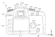
- FIG. 1 is a diagram illustrating an external configuration of an imaging apparatus 1 according to an embodiment of the present invention.
- FIG. 2 is a diagram illustrating an external configuration of the imaging apparatus 1.
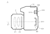
- FIG. 3 is a longitudinal sectional view of the imaging apparatus 1.
- FIG. 4 is a block diagram illustrating an electrical configuration of the imaging apparatus 1.
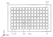
- FIG. 5 is a diagram for explaining the configuration of the image sensor 101.
- FIG. 6 is a diagram for explaining the configuration of the image sensor 101.
- FIG. 7 is a longitudinal sectional view for explaining the configuration of the AF pixel pair 11f.
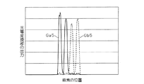
- FIG. 8 is a diagram illustrating a simulation result when the focal plane is defocused closer to 200 ⁇ m from the imaging plane of the imaging element 101.
- FIG. 1 is a diagram illustrating an external configuration of an imaging apparatus 1 according to an embodiment of the present invention.
- FIG. 2 is a diagram illustrating an external configuration of the imaging apparatus 1.
- FIG. 3 is a longitudinal sectional view of the imaging apparatus 1.
- FIG. 4 is
- FIG. 9 is a diagram illustrating a simulation result when the focal plane is defocused to the near side of 100 ⁇ m from the imaging surface.
- FIG. 10 is a diagram illustrating a simulation result in a focused state where the focal plane coincides with the imaging surface.
- FIG. 11 is a diagram showing a simulation result when the focal plane is defocused 100 ⁇ m away from the imaging surface.
- FIG. 12 is a diagram illustrating a simulation result in a case where the focal plane is defocused on the far side of 200 ⁇ m from the imaging surface.
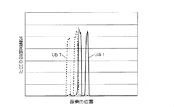
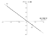
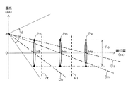
- FIG. 13 is a diagram for explaining a graph Gc showing the relationship between the difference between the center of gravity positions and the defocus amount in a pair of image rows.
- FIG. 10 is a diagram illustrating a simulation result in a focused state where the focal plane coincides with the imaging surface.
- FIG. 11 is a diagram showing a simulation result when the focal plane is defocused 100 ⁇ m away from the imaging surface.
- FIG. 12 is a diagram illustrating a simulation result
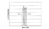
- FIG. 14 is a diagram for explaining an unbalance of pupil division that occurs in accordance with the exit pupil position of the interchangeable lens 2.
- FIG. 15 is a conceptual diagram for explaining the configuration of the AF pixel pair 11g.
- FIG. 16 is a diagram for explaining distance measurement control according to the exit pupil position of the interchangeable lens 2.
- FIG. 17 is a conceptual diagram for explaining the configuration of the AF pixel pair 11j.
- FIG. 18 is a conceptual diagram for explaining the configuration of the AF pixel pair 11k.
- FIG. 19 is a diagram for explaining the AF lines Lj, Lg, and Lk for far-distance, in-pupil, and near-pupil.
- FIG. 20 is a flowchart showing the basic operation of the imaging apparatus 1.
- FIG. 21 is a diagram for explaining the configuration of an AF pixel pair 11fa according to a modification of the present invention.
- FIGS. 1 and 2 show a front view and a rear view, respectively.
- the imaging apparatus 1 is configured as, for example, a single-lens reflex digital still camera, and includes a camera body 10 and an interchangeable lens 2 as a photographic lens that is detachable from the camera body 10.
- a mount portion 301 to which the interchangeable lens 2 is mounted at the center of the front surface a lens exchange button 302 disposed on the right side of the mount portion 301, and a gripper.
- FIG. 2 on the rear side of the camera body 10, there are an LCD (Liquid Crystal Display) 311, a setting button group 312 disposed on the left side of the LCD 311, and a cross key 314 disposed on the right side of the LCD 311. And a push button 315 disposed in the center of the cross key 314.
- an EVF Electronic View Finder
- 316 disposed above the LCD 311, an eye cup 321 surrounding the EVF 316, and a main switch 317 disposed on the left side of the EVF 316.
- An exposure correction button 323 and an AE lock button 324 disposed on the right side of the EVF 316, and a flash unit 318 and a connection terminal unit 319 disposed above the EVF 316.
- the mount part 301 is provided with a connector Ec (see FIG. 4) for electrical connection with the mounted interchangeable lens 2 and a coupler 75 (see FIG. 4) for mechanical connection.
- the lens exchange button 302 is a button that is pressed when the interchangeable lens 2 mounted on the mount unit 301 is removed.
- the grip part 303 is a part where the user grips the image pickup apparatus 1 at the time of photographing, and is provided with surface irregularities adapted to the finger shape in order to improve fitting properties.
- a battery storage chamber and a card storage chamber are provided inside the grip portion 303.
- a battery 69B (see FIG. 4) is housed in the battery compartment as a power source for the camera, and a memory card 67 (see FIG. 4) for recording image data of the photographed image is detachably housed in the card compartment. It has come to be.
- the grip unit 303 may be provided with a grip sensor for detecting whether or not the user has gripped the grip unit 303.
- the mode setting dial 305 and the control value setting dial 306 are made of a substantially disk-shaped member that can rotate in a plane substantially parallel to the upper surface of the camera body 10.
- the mode setting dial 305 is used for various types of shooting such as an automatic exposure (AE) control mode, an autofocus (AF) control mode, a still image shooting mode for shooting a single still image, and a continuous shooting mode for continuous shooting.
- This mode is used to selectively select a mode and a function installed in the imaging apparatus 1, such as a mode and a reproduction mode for reproducing a recorded image.
- the control value setting dial 306 is for setting control values for various functions installed in the imaging apparatus 1.
- the shutter button 307 is a push-down switch that can be operated in a “half-pressed state” that is pressed halfway and further operated in a “full-pressed state”.
- a preparatory operation for setting an exposure control value, focus detection, etc.
- a photographing operation (a series of operations for exposing the image sensor 101 (see FIG. 3), performing predetermined image processing on the image signal obtained by the exposure, and recording the image signal on a memory card or the like) is performed.
- the LCD 311 includes a color liquid crystal panel capable of displaying an image.
- the LCD 311 displays an image picked up by the image pickup device 101 (see FIG. 3), reproduces and displays a recorded image, and is mounted on the image pickup apparatus 1. Function and mode setting screen. Note that an organic EL or a plasma display device may be used instead of the LCD 311.
- the setting button group 312 is a button for performing operations on various functions installed in the imaging apparatus 1.
- the setting button group 312 includes, for example, a selection confirmation switch for confirming the content selected on the menu screen displayed on the LCD 311, a selection cancel switch, a menu display switch for switching the content of the menu screen, a display on / off switch, A display enlargement switch is included.
- the cross key 314 has an annular member having a plurality of pressing portions (triangle marks in the figure) arranged at regular intervals in the circumferential direction, and is not shown and provided corresponding to each pressing portion.
- the pressing operation of the pressing portion is detected by the contact (switch).
- the push button 315 is arranged at the center of the cross key 314.
- the cross key 314 and the push button 315 are used to change the shooting magnification (movement of the zoom lens 212 (see FIG. 4) in the wide direction or the tele direction), frame-by-frame feeding of a recorded image to be reproduced on the LCD 311 and the like, and shooting conditions (aperture value). , Shutter speed, presence / absence of flash emission, etc.) for inputting instructions.
- the EVF 316 includes a liquid crystal panel 310 (see FIG. 3), and displays an image captured by the image sensor 101 (see FIG. 3), reproduces and displays a recorded image, and the like.
- live view (preview) display that displays a subject in a moving image mode based on image signals sequentially generated by the image sensor 101 before actual shooting (shooting for image recording) is performed. The user can visually recognize a subject actually captured by the image sensor 101.
- the main switch 317 is a two-contact slide switch that slides to the left and right. When the switch is set to the left, the power of the imaging device 1 is turned on, and when the switch is set to the right, the power is turned off.
- the flash unit 318 is configured as a pop-up built-in flash. On the other hand, when attaching an external flash or the like to the camera body 10, the connection is made using the connection terminal portion 319.
- the eye cup 321 is a “U” -shaped light shielding member that has light shielding properties and suppresses intrusion of external light into the EVF 316.
- the exposure correction button 323 is a button for manually adjusting the exposure value (aperture value and shutter speed), and the AE lock button 324 is a button for fixing the exposure.
- the interchangeable lens 2 functions as a lens window that captures light (light image) from a subject, and also functions as a photographing optical system that guides the subject light to the image sensor 101 disposed inside the camera body 10. It is.
- the interchangeable lens 2 can be detached from the camera body 10 by depressing the lens interchange button 302 described above.
- the interchangeable lens 2 includes a lens group 21 including a plurality of lenses arranged in series along the optical axis LT (see FIG. 4).
- the lens group 21 includes a focus lens 211 (see FIG. 4) for adjusting the focal point and a zoom lens 212 (see FIG. 4) for zooming, and each includes an optical axis LT ( By driving in the direction (see FIG. 3), zooming and focus adjustment are performed.
- the interchangeable lens 2 is provided with an operation ring that can rotate along the outer peripheral surface of the lens barrel at a suitable position on the outer periphery of the lens barrel.
- the zoom lens 212 can be operated by manual operation or automatic operation. It moves in the optical axis direction according to the rotation direction and rotation amount of the operation ring, and is set to a zoom magnification (imaging magnification) according to the position of the movement destination.
- FIG. 3 is a longitudinal sectional view of the imaging apparatus 1.
- the camera body 10 includes an image sensor 101, an EVF 316, and the like.
- the imaging element 101 is arranged in a direction perpendicular to the optical axis LT on the optical axis LT of the lens group included in the interchangeable lens 2 when the interchangeable lens 2 is attached to the camera body 10.
- the image sensor 101 for example, a CMOS color area sensor (CMOS type image sensor) in which a plurality of pixels configured with photodiodes are two-dimensionally arranged in a matrix is used.
- the imaging device 101 generates analog electrical signals (image signals) of R (red), G (green), and B (blue) color components related to the subject luminous flux received through the interchangeable lens 2, and R, G, Output as B color image signals.
- the configuration of the image sensor 101 will be described in detail later.
- a shutter unit 40 is disposed in front of the image sensor 101 in the optical axis direction.
- the shutter unit 40 includes a curtain body that moves in the vertical direction, and a mechanical focal plane that performs an optical path opening operation and an optical path blocking operation of subject light guided to the image sensor 101 along the optical axis LT by the opening operation and the closing operation. It is configured as a shutter.
- the shutter unit 40 can be omitted when the image sensor 101 is an image sensor capable of complete electronic shutter.
- the EVF 316 includes a liquid crystal panel 310 and an eyepiece lens 106.
- the liquid crystal panel 310 is configured as a color liquid crystal panel capable of displaying an image, for example, and can display an image captured by the image sensor 101.
- the eyepiece 106 guides the subject image displayed on the liquid crystal panel 310 to the outside of the EVF 316. With such a configuration of the EVF 316, the user can visually recognize a subject photographed by the image sensor 101.
- FIG. 4 is a block diagram illustrating an electrical configuration of the imaging apparatus 1.
- the same members as those in FIGS. 1 to 3 are denoted by the same reference numerals.
- the electrical configuration of the interchangeable lens 2 will be described first.
- the interchangeable lens 2 includes a lens drive mechanism 24, a lens position detection unit 25, a lens control unit 26, and an aperture drive mechanism 27 in addition to the lens group 21 constituting the photographing optical system described above.
- a focus lens 211 and a zoom lens 212, and a diaphragm 23 for adjusting the amount of light incident on the image sensor 101 provided in the camera body 10 are arranged in an optical axis LT (FIG. 3) in the lens barrel.
- the optical image of the subject is captured and formed on the image sensor 101.
- focus adjustment is performed by driving the focus lens 211 in the optical axis LT direction by the AF actuator 71M in the interchangeable lens 2.
- the focus drive control unit 71A generates a drive control signal for the AF actuator 71M necessary for moving the focus lens 211 to the in-focus position based on the AF control signal given from the main control unit 62 via the lens control unit 26. Is to be generated.
- the AF actuator 71M is composed of a stepping motor or the like, and applies a lens driving force to the lens driving mechanism 24.
- the lens driving mechanism 24 includes, for example, a helicoid and a gear (not shown) that rotates the helicoid, and receives the driving force from the AF actuator 71M to drive the focus lens 211 and the like in a direction parallel to the optical axis LT. It is. Note that the movement direction and the movement amount of the focus lens 211 are in accordance with the rotation direction and the rotation speed of the AF actuator 71M, respectively.
- the lens position detection unit 25 moves integrally with the lens while being in sliding contact with the encode plate in which a plurality of code patterns are formed at a predetermined pitch in the optical axis LT direction within the movement range of the lens group 21.
- An encoder brush and detects the amount of movement of the lens group 21 during focus adjustment.
- the lens position detected by the lens position detection unit 25 is output as the number of pulses, for example.
- the lens control unit 26 is composed of a microcomputer having a built-in memory such as a ROM for storing a control program or the like and a flash memory for storing data relating to status information. Information on the exit pupil position of the interchangeable lens 2 described later is stored in the ROM in the lens control unit 26.
- the lens control unit 26 has a communication function for performing communication with the main control unit 62 of the camera body 10 via the connector Ec.
- the state information data such as the focal length, the exit pupil position, the aperture value, the focusing distance, and the peripheral light amount state of the lens group 21 and the position information of the focus lens 211 detected by the lens position detection unit 25 are main-controlled.
- the driving amount data of the focus lens 211 can be received from the main control unit 62.
- the aperture drive mechanism 27 receives the driving force from the aperture drive actuator 76M via the coupler 75 and changes the aperture diameter of the aperture 23.
- the camera body 10 includes an AFE (analog front end) 5, an image processing unit 61, an image memory 614, a main control unit 62, a flash circuit 63, an operation unit, in addition to the imaging element 101 and the shutter unit 40 described above. 64, VRAM 65 (65a, 65b), card interface (I / F) 66, memory card 67, communication interface (I / F) 68, power supply circuit 69, battery 69B, shutter drive control unit 73A, and shutter drive actuator 73M
- the aperture drive controller 76A and the aperture drive actuator 76M are provided.
- the image sensor 101 is composed of a CMOS color area sensor as described above, and the timing control circuit 51 described below starts (and ends) the exposure operation of the image sensor 101 and selects the output of each pixel included in the image sensor 101.
- the imaging operation such as readout of the pixel signal is controlled.
- the AFE 5 gives a timing pulse for causing the image sensor 101 to perform a predetermined operation, and performs predetermined signal processing on an image signal (analog signal group received by each pixel of the CMOS area sensor) output from the image sensor 101. Is converted into a digital signal and output to the image processing unit 61.
- the AFE 5 includes a timing control circuit 51, a signal processing unit 52, an A / D conversion unit 53, and the like.
- the timing control circuit 51 generates a predetermined timing pulse (a pulse for generating a vertical scanning pulse ⁇ Vn, a horizontal scanning pulse ⁇ Vm, a reset signal ⁇ Vr, etc.) based on the reference clock output from the main control unit 62, and the imaging device 101. And the imaging operation of the image sensor 101 is controlled. In addition, the operation of the signal processing unit 52 and the A / D conversion unit 53 is controlled by outputting predetermined timing pulses to the signal processing unit 52 and the A / D conversion unit 53, respectively.
- a predetermined timing pulse a pulse for generating a vertical scanning pulse ⁇ Vn, a horizontal scanning pulse ⁇ Vm, a reset signal ⁇ Vr, etc.
- the signal processing unit 52 performs predetermined analog signal processing on the analog image signal output from the image sensor 101.
- the signal processing unit 52 includes a CDS (correlated double sampling) circuit, an AGC (auto gain control) circuit, a clamp circuit, and the like.
- the A / D conversion unit 53 converts the analog R, G, B image signals output from the signal processing unit 52 into a plurality of bits (for example, 12 bits) based on the timing pulse output from the timing control circuit 51. Is converted into a digital image signal.
- the image processing unit 61 performs predetermined signal processing on the image data output from the AFE 5 to create an image file, and includes a black level correction circuit 611, a white balance control circuit 612, a gamma correction circuit 613, and the like. Has been.
- the image data captured by the image processing unit 61 is temporarily written in the image memory 614 in synchronization with the reading of the image sensor 101. Thereafter, the image data written in the image memory 614 is accessed to access the image processing unit. Processing is performed in each of the 61 blocks.
- the black level correction circuit 611 corrects the black level of each of the R, G, and B digital image signals A / D converted by the A / D converter 53 to a reference black level.
- the white balance control circuit 612 performs digital signal level conversion (white balance (WB) adjustment) of each color component of R (red), G (green), and B (blue) based on the white standard corresponding to the light source. Is what you do. That is, the white balance control circuit 612 identifies a portion that is originally estimated to be white based on luminance, saturation data, and the like in the photographic subject based on the WB adjustment data provided from the main control unit 62, and R, G of that portion. , B, the average of the color components, the G / R ratio and the G / B ratio are obtained, and the levels are corrected as R and B correction gains.
- WB white balance
- the gamma correction circuit 613 corrects the gradation characteristics of the WB adjusted image data. Specifically, the gamma correction circuit 613 performs non-linear conversion and offset adjustment using a gamma correction table set in advance for each color component.
- the image memory 614 temporarily stores the image data output from the image processing unit 61 in the shooting mode, and is used as a work area for performing predetermined processing on the image data by the main control unit 62. It is memory. In the playback mode, the image data read from the memory card 67 is temporarily stored.
- the main control unit 62 is composed of a microcomputer having a built-in storage unit such as a ROM for storing a control program and a RAM for temporarily storing data, and controls the operation of each unit of the imaging apparatus 1.
- the flash circuit 63 controls the light emission amount of the external flash connected to the flash unit 318 or the connection terminal unit 319 to the light emission amount set by the main control unit 62 in the flash photographing mode.
- the operation unit 64 includes the mode setting dial 305, the control value setting dial 306, the shutter button 307, the setting button group 312, the cross key 314, the push button 315, the main switch 317, etc., and the operation information is sent to the main control unit 62. It is for input.
- the VRAMs 65a and 65b have a storage capacity of image signals corresponding to the number of pixels of the LCD 311 and the EVF 316, and are buffer memories between the main control unit 62 and the LCD 311 and the EVF 316.
- the card I / F 66 is an interface for enabling transmission / reception of signals between the memory card 67 and the main control unit 62.
- the memory card 67 is a recording medium that stores image data generated by the main control unit 62.
- the communication I / F 68 is an interface for enabling transmission of image data and the like to a personal computer and other external devices.
- the power supply circuit 69 includes, for example, a constant voltage circuit, and generates a voltage for driving the entire imaging apparatus 1 such as a control unit such as the main control unit 62, the image sensor 101, and other various driving units. Note that energization control to the image sensor 101 is performed by a control signal supplied from the main control unit 62 to the power supply circuit 69.
- the battery 69B includes a primary battery such as an alkaline battery or a secondary battery such as a nickel metal hydride battery, and is a power source that supplies power to the entire imaging apparatus 1.
- the shutter drive control unit 73A generates a drive control signal for the shutter drive actuator 73M based on a control signal given from the main control unit 62.
- the shutter drive actuator 73M is an actuator that performs opening / closing drive of the shutter unit 40.
- the aperture drive control unit 76A generates a drive control signal for the aperture drive actuator 76M based on the control signal given from the main control unit 62.
- the aperture driving actuator 76M applies a driving force to the aperture driving mechanism 27 via the coupler 75.
- the camera body 10 is based on the black level corrected image data output from the black level correction circuit 611 and performs a phase difference AF calculation circuit 77 that performs a calculation necessary for autofocus (AF) control using the image sensor 101. It has.
- phase difference AF operation of the imaging apparatus 1 using the phase difference AF calculation circuit 77 will be described in detail.
- the imaging apparatus 1 is configured to be capable of phase difference AF by receiving transmitted light that has been transmitted (passed) through different portions of the exit pupil in the imaging element 101.
- the configuration of the image sensor 101 and the principle of phase difference AF using the image sensor 101 will be described below.
- FIG. 5 and 6 are diagrams for explaining the configuration of the image sensor 101.
- FIG. 5 and 6 are diagrams for explaining the configuration of the image sensor 101.
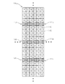
- the imaging device 101 has a configuration capable of detecting a focus of the phase difference detection method in each of a plurality of AF areas Ef defined in a matrix on the imaging surface 101f (FIG. 5).
- Each AF area Ef has a normal pixel composed of an R pixel 111, a G pixel 112, and a B pixel 113 in which R (red), G (green), and B (blue) color filters are arranged on a photodiode.
- normal pixel 110 is provided, and a pair of pixels (hereinafter referred to as “AF pixel”) for performing phase difference AF having lower light shielding masks 12a and 12c (parallel oblique line portions) described later.
- 11f also referred to as “pair” is provided (FIG. 6).
- the Gr line L1 in which the G pixel 112 and the R pixel 111 are alternately arranged in the horizontal direction as the horizontal line of the normal pixel 110, and the B pixel 113 and the G pixel 112 are alternately arranged in the horizontal direction. And a Gb line L2 arranged at the same position.
- a Bayer arrangement is configured by alternately arranging the Gr lines L1 and Gb lines L2 in the vertical direction.
- AF lines (focus detection pixel arrays) Lf in which AF pixel pairs 11f are repeatedly arranged in the horizontal direction are periodically formed in the vertical direction.
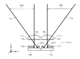
- FIG. 7 is a longitudinal sectional view for explaining the configuration of the AF pixel pair 11f.
- the AF pixel pair 11f shown in FIG. 7 is provided in the AF area Ef (for example, the AF area Efo shown in FIG. 5) located near the center of the imaging surface 101f.
- the positions of the openings OPa to OPb and OPc to OPd for separating the light beam Ta from the left portion Qa of the exit pupil and the light beam Tb from the right portion Qb of the interchangeable lens 2 are mirror targets.
- a pair of pixels 11a and 11b having two light-shielding masks (light-shielding plates) 12a to 12b and 12c to 12d, and two or more AF pixel pairs 11f are arranged along the horizontal direction to achieve AF.
- a line Lf is formed.
- first AF pixel a rectangular (slit-shaped) opening OPa that is biased to the right side with respect to the photoelectric conversion portion (photodiode) PD has a lower light shielding mask.
- a slit-like opening OPb that is formed in 12a and is biased to the left with respect to the photoelectric conversion portion PD is provided in the upper light shielding mask 12b.
- the light-transmitting portions of the light-shielding portion 121 including the light-shielding mask 12a and the light-shielding mask 12b are configured by the openings OPa and OPb, and the left-side portion Qa is defined in the exit pupil by the light-transmitting portions.
- the pixel hereinafter also referred to as “second AF pixel” 11b
- a slit-shaped opening OPc that is biased to the left with respect to the photoelectric conversion unit PD is formed in the lower light shielding mask 12c, and the photoelectric conversion unit PD.
- a slit-like opening OPd biased to the right side is provided in the upper light shielding mask 12d.
- the light-transmitting portions of the light-shielding portion 122 including the light-shielding mask 12c and the light-shielding mask 12d are configured by the openings OPc and OPd, and the right-side portion Qb of the exit pupil is defined by the light-transmitting portions.
- Such first AF pixels 11a and second AF pixels 11b are alternately arranged on the AF line Lf as shown in FIG.
- pupil division at the exit pupil that is, the light beam Ta from the left portion Qa of the exit pupil causes the apertures (light transmission) of the microlens ML, the color filter FR, and the light shielding masks 12a and 12b.
- the light passes through OPa and OPb and is received by the photoelectric conversion unit PD of the first AF pixel 11a, and the light flux Tb from the right part Qb of the exit pupil is reflected by the microlens ML, the color filter FR, and the light shielding masks 12c and 12d.
- the light passes through the openings (light transmission portions) OPc and OPd and is received by the photoelectric conversion unit PD of the second AF pixel 11b.
- the left side portion (first partial region) Qa and the right side portion (second partial region) that are biased in the left and right directions opposite to each other in the exit pupil of the interchangeable lens 2 are shown.
- Light fluxes Ta and Tb of the subject passing through Qb are received.
- the light reception data obtained in the first AF pixel 11a is referred to as “A series data”
- the light reception data obtained in the second AF pixel 11b is referred to as “B series data”.
- the principle of phase difference AF will be described with reference to FIGS. 8 to 12 showing A-series data and B-series data obtained from a group of AF pixel pairs 11f arranged in Lf (FIG. 6).
- FIG. 8 is a diagram illustrating a simulation result when the focal plane is defocused closer to the 200 ⁇ m side from the imaging surface 101f of the imaging element 101
- FIG. 9 is a diagram illustrating the focal plane being closer to the 100 ⁇ m side from the imaging surface 101f. It is a figure which shows the simulation result in the case of being focused.
- FIG. 10 is a diagram illustrating a simulation result in a focused state in which the focal plane coincides with the imaging surface 101f.
- FIG. 11 is a diagram showing a simulation result when the focal plane is defocused 100 ⁇ m away from the imaging plane 101 f
- FIG. 12 is a diagram showing the focal plane defocused 200 ⁇ m away from the imaging plane 101 f.
- the horizontal axis indicates the difference (pixel pitch) of the center of gravity of the B-sequence image sequence to the center of gravity of the A-sequence image sequence
- the vertical axis indicates the defocus amount ( ⁇ m).
- the center-of-gravity position X g for each image column for example, be determined by the following calculation formula (1).
- X 1 to X n represent pixel positions from the left end in the AF line Lf, for example, and Y 1 to Y n represent the first AF pixel 11a at the positions X 1 to X n , the first The output value from the 2AF pixel 11b is shown.
- the relationship between the difference between the center of gravity positions and the defocus amount in the pair of image rows is a proportional relationship.
- This relationship can be expressed by the following equation (2) when the defocus amount is DF ( ⁇ m) and the difference in the center of gravity is C ( ⁇ m).
- the coefficient k in the above equation (2) represents a gradient Gk (shown by a broken line) with respect to the graph Gc in FIG. 13 and can be obtained in advance by a factory test or the like.
- phase difference AF calculation circuit 77 obtains the difference (phase difference) between the gravity center positions of the A-sequence data and the B-sequence data obtained from the AF pixel pair 11f
- the above equation (2) is used.
- autofocus (AF) control for moving the focus lens 211 to the detected focal position becomes possible.
- the relationship between the defocus amount and the drive amount of the focus lens 211 is uniquely determined from the design value of the interchangeable lens 2 attached to the camera body 10.
- distance measurement control is performed in accordance with the exit pupil position of the interchangeable lens 2 attached to the camera body 10 with high accuracy.
- the phase difference AF is realized, the distance measurement control will be described in detail below.
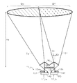
- FIG. 14 is a diagram for explaining an unbalance of pupil division that occurs in accordance with the exit pupil position of the interchangeable lens 2.
- the horizontal axis indicates the position of the exit pupil with respect to the imaging surface 101f
- the vertical axis indicates the optical axis of the interchangeable lens 2, that is, the distance (image height) from the center of the imaging surface 101f.
- the range of the entrance pupil (OCL entrance pupil) of the microlens ML related to the pixel arranged at the position of the image height ⁇ [mm] is indicated by an angle ⁇ .
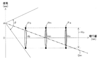
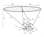
- the imaging element 101f In the imaging device 101, even in the AF pixel pair having an image height ⁇ [mm] provided in the AF area Ef (for example, the AF area Efa shown in FIG. 5) at a position away from the center of the imaging surface 101f, the imaging element 101f It is configured so that appropriate pupil division can be performed at a standard exit pupil position Pm at a distance Hm (for example, about 80 to 90 mm). Specifically, as shown in the conceptual diagram of FIG. 15, in the AF pixel pair 11g in the AF area Efa, for example, the left end of the lower light shielding mask 13c in the right pixel 11gb is the distance Ea from the center Co of the photoelectric conversion unit PD.
- the light beams Tc and Td passing through the left part Qc and the right part Qd obtained by dividing the exit pupil of the pupil diameter Ro formed at the distance Hm from the imaging surface 101f into two equal parts are converted into the photoelectric conversion parts PD.
- the pupil division line Dm extending in the oblique direction with respect to the perpendicular to the imaging surface 101f is set.
- the pupil division can be performed equally at the exit pupil at a position (hereinafter also referred to as “middle position”) Pm away from the surface 101f by a distance Hm.
- the interchangeable lens 2 there is a lens whose exit pupil position is significantly different from the position Pm described above.
- the exit pupil is formed at the position (hereinafter also referred to as “near position”) Pb
- the size of each divided region is as follows. An imbalance occurs. This makes it impossible to generate A-series and B-series pixel signals in a well-balanced manner with an AF pixel pair, making accurate ranging (focus detection) difficult.
- the imaging apparatus 1 when the interchangeable lens 2 having the exit pupil at the far position Pa is attached to the camera body 10 as shown in FIG. 16, the pupil division line corresponding to the exit pupil position. Distance measurement is performed using an AF pixel pair 11j in which Da is defined. Specifically, as shown in the conceptual diagram of FIG.
- the left end of the lower light shielding mask 13c in the right pixel 11jb is separated from the center Co of the photoelectric conversion unit PD by a distance Eb (where Eb ⁇ Ea ) Only on the right side, and the configuration of the light transmission part in the light shielding part 131 composed of the two light shielding masks 13a and 13b and the light shielding part 132 composed of the two light shielding masks 13c and 13d is compared with the AF pixel pair 11g.
- the respective light beams Te and Tf passing through the left part Qe and the right part Qf obtained by dividing the exit pupil formed at the distance Ha from the imaging surface 101f into two equal parts can be received by each photoelectric conversion unit PD. ing. Accordingly, as shown in FIG. 16, in the AF pixel pair 11j arranged at the position of the image height ⁇ [mm], the pupil division line Da whose inclination is gentler than that of the pupil division line Dm is set. The pupil division can be equally performed at the exit pupil.
- Distance measurement is performed using an AF pixel pair 11k in which Db is defined. Specifically, as shown in the conceptual diagram of FIG.
- the left end of the lower light shielding mask 13c in the right pixel 11kb is separated from the center Co of the photoelectric conversion unit PD by a distance Ec (where Ec> Ea ) Is set to the right side, and the right end of the lower light shielding mask 13a in the left pixel 11ka is set to the right side by the distance Ed from the center Co of the photoelectric conversion unit PD, and the configuration of the light transmitting portions in the light shielding units 131 and 132 is set as described above.
- the light fluxes Tg and Th passing through the left part Qg and the right part Qh obtained by dividing the exit pupil formed at the distance Hb from the imaging surface 101f into two equal parts are converted into photoelectric conversions.
- the part PD can receive light.
- the pupil division line Db whose inclination is steeper than the pupil division line Dm is set.
- the pupil division can be equally performed at the exit pupil.
- AF line Lj for the far pupil where the AF pixel pair 11j corresponding to the pupil is arranged in the horizontal direction
- AF line Lg for the pupil where the AF pixel pair 11g corresponding to the exit pupil at the middle position Pm is arranged in the horizontal direction.
- an AF line Lk near the pupil in which AF pixel pairs 11k corresponding to the exit pupil at the near position Pb are arranged in the horizontal direction are periodically provided in the vertical direction with four horizontal lines of the normal pixel 110 interposed therebetween, and exchanged.
- Ranging control that selectively uses the AF lines Lg, Lj, and Lk according to the exit pupil position of the lens 2 is performed.
- the distance Ps (for example, 110 mm) and the distance Pt (for example, 60 mm) from the imaging surface 101f are set as thresholds, and the interchangeable lens 2 at the exit pupil position that is equal to or greater than the distance Ps is attached.
- the far-distance AF line Lj is selected, and when the interchangeable lens 2 at the exit pupil position that is equal to or less than the distance Pt is attached, the near-pupil AF line Lk is selected, while the distance Pt and the distance are selected.
- the pupil AF line Lg is selected, and distance measurement is performed using the selected AF line.
- the AF lines Lg, Lj, and Lk provided in the AF area Efa include three types of pixel pairs 11g, 11j, and 11k in which the dislocation angle of the exit pupil is changed by changing the arrangement of the light transmission regions in the light shielding portions 131 and 132.
- the AF pixel pair corresponding to the exit pupil position is changed into three types of pixel pairs 11g, 11j,
- 11k By selecting from 11k, pupil division can be performed in a well-balanced manner, and focus detection by the phase difference detection method can be performed with high accuracy.
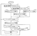
- FIG. 20 is a flowchart showing the basic operation of the imaging apparatus 1. The operation of the imaging apparatus 1 is executed by the main control unit 62.
- step ST1 When the power of the imaging device 1 is turned on by a user operation on the main switch 317, it is determined whether the exit pupil position of the interchangeable lens 2 is 60 mm or less from the imaging surface 101f (step ST1). Specifically, information on the exit pupil position of the interchangeable lens 2 stored in the ROM in the lens control unit 26 is acquired by the main control unit 62 of the camera body 10 to determine whether the exit pupil position is 60 mm or less. Is done. If the exit pupil position is 60 mm or less, the process proceeds to step ST3. If the exit pupil position is not 60 mm or less, the process proceeds to step ST2.
- step ST2 it is determined whether the exit pupil position of the interchangeable lens 2 is within the range of 60 to 110 mm from the imaging surface 101f. If the exit pupil position is within the range of 60 to 110 mm, the process proceeds to step ST4. If the exit pupil position is 110 mm or more, the process proceeds to step ST4.
- step ST3 the near-pupil AF line Lk provided with the AF pixel pair 11k shown in FIG. 18 is selected.
- step ST4 the AF line Lm for the pupil where the AF pixel pair 11g shown in FIG. 15 is arranged is selected.
- step ST5 an AF line Lj for pupil distance in which the AF pixel pair 11j shown in FIG. 17 is arranged is selected.
- step ST6 it is determined whether the shutter button 307 is half-pressed by the user. If it is half-pressed, the process proceeds to step ST7. If it is not half-pressed, the process returns to step ST1.
- step ST7 distance measurement is performed using the AF line selected in steps ST3 to ST5. That is, one type of pixel pair is selected from three types of pixel pairs 11g, 11j, and 11k in accordance with the exit pupil position with respect to the image sensor 101, and a phase difference detection method is performed based on pixel signals generated by the one type of pixel pair. Focus detection is performed. Thereby, it is possible to perform good focus detection corresponding to different exit pupil positions for each interchangeable lens.
- step ST8 it is determined whether the shutter button 307 has been fully pressed by the user. Here, if it is fully pressed, the process proceeds to step ST10. If it is not fully pressed, the process proceeds to step ST9.
- step ST9 it is determined whether the shutter button 307 is half-pressed by the user. If it is half-pressed, the process proceeds to step ST8. If it is not half-pressed, the process returns to step ST1.
- step ST10 shooting is performed. That is, the main photographing operation for generating photographing image data for recording by the image sensor 101 is performed.
- the imaging device 1 described above is provided with the imaging element 101 including the AF pixel pairs 11g, 11j, and 11k that can bisect the exit pupils at the positions Pm, Pa, and Pb shown in FIG.
- the imaging element 101 including the AF pixel pairs 11g, 11j, and 11k that can bisect the exit pupils at the positions Pm, Pa, and Pb shown in FIG.
- the pixel 11a including the two light shielding masks 12a and 12b and the pixel 11b including the two light shielding masks 12c and 12d as in the AF pixel pair 11f illustrated in FIG. Is not essential, and a pixel 11c having one light-shielding mask 12e in which an opening OPe is formed and one sheet in which the opening OPf is formed as in the AF pixel pair 11fa shown in FIG. And a pixel 11d having a light shielding mask 12f.
- the AF pixel pair 11fa is arranged in the AF area Efa (FIG. 5) defined at a position deviating from the vicinity of the center of the imaging surface 101f.
- the AF pixel pair for the pupil where the pupil division line Dm shown in FIG. 16 is set like the AF pixel pair 11g (FIG. 15) and the AF pixel pair 11j (FIG. 17).
- the focus detection can be performed with high accuracy by selecting the near, middle, and far AF pixel pairs according to the exit pupil position of the interchangeable lens.
- pupil division may be performed so that overlap occurs at the divided portions.
- AF pixel pairs 11g, 11j, and 11k for each interchangeable lens, and they may be used depending on the zoom state of the zoom lens. That is, the AF pixel pairs 11g, 11j, and 11k for in-pupil, far-for-pupil, and near-pupil may be used properly according to the exit pupil position that changes depending on the zoom magnification of the interchangeable lens 2.
- AF pixel pairs for pupils, for pupils, and for pupils
- two types or four or more types of AF pixel pairs Also good.
Landscapes
- Physics & Mathematics (AREA)
- General Physics & Mathematics (AREA)
- Engineering & Computer Science (AREA)
- Multimedia (AREA)
- Signal Processing (AREA)
- Optics & Photonics (AREA)
- Studio Devices (AREA)
- Focusing (AREA)
- Automatic Focus Adjustment (AREA)
- Transforming Light Signals Into Electric Signals (AREA)
Abstract
Description
図1および図2は、本発明の実施形態に係る撮像装置1の外観構成を示す図である。ここで、図1および図2は、それぞれ正面図および背面図を示している。 <Principal configuration of imaging device>
1 and 2 are diagrams showing an external configuration of an
次に、撮像装置1の内部構成について説明する。図3は、撮像装置1の縦断面図である。図3に示すように、カメラボディ10の内部には、撮像素子101、EVF316などが備えられている。 <Internal Configuration of
Next, the internal configuration of the
図4は、撮像装置1の電気的な構成を示すブロック図である。ここで、図1~図3と同一の部材等については、同一の符号を付している。なお、説明の便宜上、交換レンズ2の電気的構成について先ず説明する。 <Electrical Configuration of
FIG. 4 is a block diagram illustrating an electrical configuration of the
撮像装置1では、撮像素子101において射出瞳の異なった部分を透過(通過)した透過光を受光することにより位相差AFが可能な構成となっている。この撮像素子101の構成と、撮像素子101を利用した位相差AFの原理とを、以下で説明する。 <Regarding Phase Difference AF Operation of
The


図14は、交換レンズ2の射出瞳位置に応じて生じる瞳分割のアンバランスを説明するための図である。この図14においては、横軸が撮像面101fに対する射出瞳の位置を示しており、縦軸が交換レンズ2の光軸、つまり撮像面101fの中心からの距離(像高)を示している。なお、図14では、像高α[mm]の位置に配置された画素に関するマイクロレンズMLの入射瞳(OCL入射瞳)の範囲を角度θで示している。 <Ranging control according to the exit pupil position of the
FIG. 14 is a diagram for explaining an unbalance of pupil division that occurs in accordance with the exit pupil position of the
図20は、撮像装置1の基本的な動作を示すフローチャートである。なお、この撮像装置1の動作については、メイン制御部62で実行される。 <Operation of
FIG. 20 is a flowchart showing the basic operation of the
・上記の実施形態におけるAF画素対については、図7に示すAF画素対11fのように2枚の遮光マスク12a、12bを備えた画素11aと2枚の遮光マスク12c、12dを備えた画素11bとで構成されるのは必須でなく、図21に示すAF画素対11faのように開口部OPeが形成される1枚の遮光マスク12eを備えた画素11cと開口部OPfが形成される1枚の遮光マスク12fを備えた画素11dとで構成されても良い。 <Modification>
As for the AF pixel pair in the above-described embodiment, the
Claims (3)
- 撮像装置であって、
(a)撮影光学系と、
(b)前記撮像光学系を通った被写体光束を受光する撮像素子と、を備えるとともに、
前記撮像素子は、
前記撮影光学系の射出瞳において互いに逆方向に偏った第1の部分領域および第2の部分領域を通過した被写体光束を受光する画素対の群、を有し、
前記画素対は、前記射出瞳において前記第1の部分領域を規定する光透過部分が設けられた遮光部を有する第1画素と、前記射出瞳において前記第2の部分領域を規定する光透過部分が設けられた遮光部を有する第2画素とを備えて構成されるとともに、
前記画素対の群は、前記遮光部における光透過部分の配置を異ならせた複数種類の画素対を有しており、前記複数種類の画素対それぞれでは、前記第1の部分領域と前記第2の部分領域との面積が同等となる射出瞳の前記撮像素子に対する位置が異なっていることを特徴とする撮像装置。 An imaging device,
(a) a photographing optical system;
(b) an image sensor that receives a subject light flux that has passed through the imaging optical system, and
The image sensor is
A group of pixel pairs for receiving a subject luminous flux that has passed through a first partial region and a second partial region that are biased in opposite directions at the exit pupil of the photographing optical system;
The pixel pair includes a first pixel having a light-shielding portion provided with a light transmission portion that defines the first partial region in the exit pupil, and a light transmission portion that defines the second partial region in the exit pupil. And a second pixel having a light-shielding portion provided with
The group of pixel pairs has a plurality of types of pixel pairs in which the arrangement of light transmission portions in the light shielding portion is different, and each of the plurality of types of pixel pairs includes the first partial region and the second region. An imaging apparatus characterized in that the position of the exit pupil, which has the same area as the partial area, is different from the position of the imaging element. - 請求項1に記載の撮像装置において、
(c)前記撮像素子に対する射出瞳の位置に応じて前記複数種類の画素対から1種類の画素対を選択し、当該1種類の画素対で生成される画素信号に基づき位相差検出方式の焦点検出を行う手段、をさらに備えることを特徴とする撮像装置。 The imaging device according to claim 1,
(c) One type of pixel pair is selected from the plurality of types of pixel pairs according to the position of the exit pupil with respect to the image sensor, and the focus of the phase difference detection method is based on the pixel signal generated by the one type of pixel pair. An imaging apparatus, further comprising means for performing detection. - 撮影光学系を通った被写体光束を受光可能な撮像素子であって、
前記撮影光学系の射出瞳において互いに逆方向に偏った第1の部分領域および第2の部分領域を通過した被写体光束を受光する画素対の群、を備え、
前記画素対は、前記射出瞳において前記第1の部分領域を規定する光透過部分が設けられた遮光部を有する第1画素と、前記射出瞳において前記第2の部分領域を規定する光透過部分が設けられた遮光部を有する第2画素とを備えて構成されるとともに、
前記画素対の群は、前記遮光部における光透過部分の配置を異ならせた複数種類の画素対を有しており、前記複数種類の画素対それぞれでは、前記第1の部分領域と前記第2の部分領域との面積が同等となる射出瞳の前記撮像素子に対する位置が異なっていることを特徴とする撮像素子。 An image sensor capable of receiving a subject luminous flux that has passed through a photographing optical system,
A group of pixel pairs for receiving a subject luminous flux that has passed through a first partial region and a second partial region that are biased in opposite directions at the exit pupil of the photographing optical system,
The pixel pair includes a first pixel having a light-shielding portion provided with a light transmission portion that defines the first partial region in the exit pupil, and a light transmission portion that defines the second partial region in the exit pupil. And a second pixel having a light-shielding portion provided with
The group of pixel pairs has a plurality of types of pixel pairs in which the arrangement of light transmission portions in the light shielding portion is different, and each of the plurality of types of pixel pairs includes the first partial region and the second region. An image pickup device characterized in that the position of the exit pupil with the same area as that of the partial region is different from the position of the image pickup device.
Priority Applications (4)
| Application Number | Priority Date | Filing Date | Title |
|---|---|---|---|
| EP09715094.0A EP2249192B1 (en) | 2008-02-28 | 2009-02-26 | Imaging device, and imaging element |
| US12/735,639 US8319882B2 (en) | 2008-02-28 | 2009-02-26 | Image pickup device and image pickup element including plurality of types of pixel pairs |
| EP19151090.8A EP3489730A1 (en) | 2008-02-28 | 2009-02-26 | Image pickup device and image pickup element |
| CN2009801051900A CN101952758B (en) | 2008-02-28 | 2009-02-26 | Imaging device, and imaging element |
Applications Claiming Priority (2)
| Application Number | Priority Date | Filing Date | Title |
|---|---|---|---|
| JP2008048360A JP5050928B2 (en) | 2008-02-28 | 2008-02-28 | Imaging device and imaging device |
| JP2008-048360 | 2008-02-28 |
Publications (1)
| Publication Number | Publication Date |
|---|---|
| WO2009107705A1 true WO2009107705A1 (en) | 2009-09-03 |
Family
ID=41016093
Family Applications (1)
| Application Number | Title | Priority Date | Filing Date |
|---|---|---|---|
| PCT/JP2009/053517 WO2009107705A1 (en) | 2008-02-28 | 2009-02-26 | Imaging device, and imaging element |
Country Status (7)
| Country | Link |
|---|---|
| US (1) | US8319882B2 (en) |
| EP (2) | EP3489730A1 (en) |
| JP (1) | JP5050928B2 (en) |
| KR (1) | KR20100124717A (en) |
| CN (1) | CN101952758B (en) |
| TW (1) | TWI427351B (en) |
| WO (1) | WO2009107705A1 (en) |
Cited By (4)
| Publication number | Priority date | Publication date | Assignee | Title |
|---|---|---|---|---|
| CN102572272A (en) * | 2010-12-20 | 2012-07-11 | 索尼公司 | Image processing apparatus, image processing method and program |
| WO2013018471A1 (en) * | 2011-07-29 | 2013-02-07 | 富士フイルム株式会社 | Imaging device |
| US9124876B2 (en) | 2011-08-23 | 2015-09-01 | Fujifilm Corporation | Pupil-dividing imaging apparatus |
| US9936167B2 (en) | 2014-01-14 | 2018-04-03 | Ricoh Company, Ltd. | Imaging device, imaging method, image processing device, and recording medium storing imaging program |
Families Citing this family (47)
| Publication number | Priority date | Publication date | Assignee | Title |
|---|---|---|---|---|
| JP5593602B2 (en) * | 2008-09-24 | 2014-09-24 | ソニー株式会社 | Imaging device and imaging apparatus |
| US8913175B2 (en) | 2008-11-27 | 2014-12-16 | Canon Kabushiki Kaisha | Solid-state image sensing element and image sensing apparatus for detecting a focus state of a photographing lens |
| JP5159700B2 (en) | 2009-05-19 | 2013-03-06 | キヤノン株式会社 | Optical apparatus and focus detection method |
| JP5563283B2 (en) * | 2009-12-09 | 2014-07-30 | キヤノン株式会社 | Image processing device |
| JP5649837B2 (en) * | 2010-03-24 | 2015-01-07 | 富士フイルム株式会社 | Stereo imaging device |
| CN102870028B (en) * | 2010-04-28 | 2015-11-25 | 富士胶片株式会社 | Imaging device |
| JP5764884B2 (en) * | 2010-08-16 | 2015-08-19 | ソニー株式会社 | Imaging device and imaging apparatus |
| US9532033B2 (en) * | 2010-11-29 | 2016-12-27 | Nikon Corporation | Image sensor and imaging device |
| JP5812610B2 (en) * | 2011-01-18 | 2015-11-17 | キヤノン株式会社 | Solid-state imaging device and imaging system having solid-state imaging device |
| JP5861257B2 (en) * | 2011-02-21 | 2016-02-16 | ソニー株式会社 | Imaging device and imaging apparatus |
| JP2012182332A (en) * | 2011-03-02 | 2012-09-20 | Sony Corp | Imaging element and imaging device |
| JP5640143B2 (en) * | 2011-03-31 | 2014-12-10 | 富士フイルム株式会社 | Imaging apparatus and imaging method |
| JP5895355B2 (en) * | 2011-04-25 | 2016-03-30 | 株式会社ニコン | Imaging device |
| JP5526287B2 (en) * | 2011-04-28 | 2014-06-18 | 富士フイルム株式会社 | Imaging apparatus and imaging method |
| CN103597811B (en) * | 2011-06-09 | 2015-07-29 | 富士胶片株式会社 | Take the image-capturing element of Three-dimensional movable image and planar moving image and be equipped with its image capturing device |
| JP5885421B2 (en) * | 2011-08-10 | 2016-03-15 | オリンパス株式会社 | Imaging device |
| JP2013037296A (en) * | 2011-08-10 | 2013-02-21 | Olympus Imaging Corp | Image pickup apparatus and image pickup device |
| WO2013047160A1 (en) | 2011-09-28 | 2013-04-04 | 富士フイルム株式会社 | Solid-state image capture element, image capture device, and focus control method |
| JP5710835B2 (en) * | 2012-03-21 | 2015-04-30 | 富士フイルム株式会社 | Imaging device |
| JP5947602B2 (en) * | 2012-04-11 | 2016-07-06 | キヤノン株式会社 | Imaging device |
| JP6019692B2 (en) * | 2012-04-16 | 2016-11-02 | ソニー株式会社 | Image pickup device, image pickup device control method, and image pickup apparatus |
| JP6034629B2 (en) * | 2012-09-12 | 2016-11-30 | キヤノン株式会社 | Image pickup device and image pickup apparatus using the same |
| CN103852954B (en) * | 2012-12-03 | 2017-11-07 | 北京大学 | A kind of method for realizing phase focusing |
| CN103852955B (en) * | 2012-12-03 | 2017-12-19 | 北京大学 | A kind of device for realizing phase focusing |
| EP2782331A1 (en) * | 2013-03-22 | 2014-09-24 | Harvest Imaging bvba | Image sensor with focus-detection pixel, and method for reading focus-information |
| WO2014155812A1 (en) * | 2013-03-27 | 2014-10-02 | 富士フイルム株式会社 | Image processing device, image capturing apparatus, image processing method, and image processing program |
| JP6295526B2 (en) * | 2013-07-11 | 2018-03-20 | ソニー株式会社 | Solid-state imaging device and electronic apparatus |
| JP6300471B2 (en) * | 2013-08-28 | 2018-03-28 | キヤノン株式会社 | Driving method of imaging apparatus and driving method of imaging system |
| KR102128467B1 (en) | 2014-01-09 | 2020-07-09 | 삼성전자주식회사 | Image sensor and image photograph apparatus including image sensor |
| JP6363857B2 (en) * | 2014-03-24 | 2018-07-25 | キヤノン株式会社 | IMAGING ELEMENT, IMAGING DEVICE, IMAGE PROCESSING METHOD, AND PROGRAM |
| KR20150121564A (en) | 2014-04-21 | 2015-10-29 | 삼성전자주식회사 | Imaging device and photographing apparatus |
| US9491442B2 (en) | 2014-04-28 | 2016-11-08 | Samsung Electronics Co., Ltd. | Image processing device and mobile computing device having the same |
| KR20160010986A (en) | 2014-07-21 | 2016-01-29 | 에스케이하이닉스 주식회사 | Image sensor |
| JP6890766B2 (en) * | 2014-08-07 | 2021-06-18 | 株式会社ニコン | Detection device |
| JP2016038467A (en) * | 2014-08-07 | 2016-03-22 | 株式会社ニコン | Image pick-up element, focus detection device and imaging device |
| JP2016058451A (en) * | 2014-09-05 | 2016-04-21 | キヤノン株式会社 | Sensor and camera |
| US9769371B1 (en) | 2014-09-09 | 2017-09-19 | Amazon Technologies, Inc. | Phase detect auto-focus |
| US9549115B1 (en) | 2014-09-22 | 2017-01-17 | Amazon Technologies, Inc. | Prism array depth sensing auto-focus |
| US10778879B2 (en) | 2015-12-25 | 2020-09-15 | Nikon Corporation | Image sensor and image-capturing device that selects pixel signal for focal position |
| GB2548462B (en) * | 2016-01-29 | 2020-06-17 | Canon Kk | Image sensor and image capturing apparatus |
| JP6365568B2 (en) * | 2016-02-29 | 2018-08-01 | 株式会社ニコン | Imaging device and imaging apparatus |
| IT201600132604A1 (en) | 2016-12-30 | 2018-06-30 | Laboratorio Europeo Di Spettroscopie Non Lineari Lens | System and method of measuring the focusing of an optical instrument |
| JP2018067005A (en) * | 2017-12-07 | 2018-04-26 | 株式会社ニコン | Interchangeable lens and camera system |
| CN117270155A (en) | 2018-07-20 | 2023-12-22 | 株式会社尼康 | Imaging element and imaging device |
| WO2020138350A1 (en) | 2018-12-26 | 2020-07-02 | 株式会社ニコン | Interchangeable lens, focus detecting device, and camera body |
| JP2020046688A (en) * | 2019-12-24 | 2020-03-26 | 株式会社ニコン | Interchangeable lens and camera system |
| CN112004026B (en) * | 2020-09-01 | 2021-06-29 | 北京小米移动软件有限公司 | Phase focusing device, phase focusing method, shooting device, terminal equipment and medium |
Citations (4)
| Publication number | Priority date | Publication date | Assignee | Title |
|---|---|---|---|---|
| JP2004191629A (en) | 2002-12-11 | 2004-07-08 | Canon Inc | Focus detector |
| JP2007155929A (en) * | 2005-12-01 | 2007-06-21 | Nikon Corp | Solid-state imaging element and imaging apparatus using the same |
| JP2007189312A (en) * | 2006-01-11 | 2007-07-26 | Nikon Corp | Imaging apparatus, imaging method, and camera |
| JP2007279312A (en) * | 2006-04-05 | 2007-10-25 | Nikon Corp | Imaging element, image sensor and imaging apparatus |
Family Cites Families (24)
| Publication number | Priority date | Publication date | Assignee | Title |
|---|---|---|---|---|
| JPS57125912A (en) * | 1981-01-30 | 1982-08-05 | Nippon Kogaku Kk <Nikon> | Ttl type focus detector for camera |
| US5202718A (en) * | 1989-03-10 | 1993-04-13 | Nikon Corporation | Focus detection apparatus |
| JP3170847B2 (en) * | 1992-02-14 | 2001-05-28 | キヤノン株式会社 | Solid-state image sensor and optical device using the same |
| JPH0694987A (en) * | 1992-09-03 | 1994-04-08 | Nikon Corp | Focus detector |
| JP3491343B2 (en) * | 1994-06-29 | 2004-01-26 | 株式会社ニコン | Focus detection device and focus detection method |
| GB2298331B (en) * | 1995-02-22 | 2000-02-16 | Asahi Optical Co Ltd | Distance measuring apparatus |
| US5598964A (en) * | 1995-09-29 | 1997-02-04 | Motorola, Inc. | Apparatus for ultrasonic welding of battery assemblies |
| JP3592147B2 (en) * | 1998-08-20 | 2004-11-24 | キヤノン株式会社 | Solid-state imaging device |
| US6518640B2 (en) * | 1999-12-02 | 2003-02-11 | Nikon Corporation | Solid-state image sensor, production method of the same, and digital camera |
| US6995800B2 (en) * | 2000-01-27 | 2006-02-07 | Canon Kabushiki Kaisha | Image pickup apparatus utilizing a plurality of converging lenses |
| JP4908668B2 (en) * | 2000-04-19 | 2012-04-04 | キヤノン株式会社 | Focus detection device |
| JP4500434B2 (en) * | 2000-11-28 | 2010-07-14 | キヤノン株式会社 | Imaging apparatus, imaging system, and imaging method |
| JP2004212431A (en) * | 2002-12-27 | 2004-07-29 | Casio Comput Co Ltd | Autofocus apparatus and autofocus method |
| WO2005081020A1 (en) * | 2004-02-19 | 2005-09-01 | Canon Kabushiki Kaisha | Optical device and beam splitter |
| JP4532968B2 (en) * | 2004-04-13 | 2010-08-25 | キヤノン株式会社 | Focus detection device |
| EP1684503B1 (en) * | 2005-01-25 | 2016-01-13 | Canon Kabushiki Kaisha | Camera and autofocus control method therefor |
| WO2006129677A1 (en) * | 2005-05-30 | 2006-12-07 | Nikon Corporation | Image formation state detection device |
| JP4720508B2 (en) * | 2006-01-05 | 2011-07-13 | 株式会社ニコン | Imaging device and imaging apparatus |
| US7751700B2 (en) * | 2006-03-01 | 2010-07-06 | Nikon Corporation | Focus adjustment device, imaging device and focus adjustment method |
| US7711261B2 (en) * | 2006-04-11 | 2010-05-04 | Nikon Corporation | Imaging device, camera and image processing method |
| JP5003132B2 (en) * | 2006-12-07 | 2012-08-15 | ソニー株式会社 | Imaging device and imaging apparatus |
| JP4973273B2 (en) * | 2007-03-28 | 2012-07-11 | 株式会社ニコン | Digital camera |
| WO2008132812A1 (en) * | 2007-04-20 | 2008-11-06 | Nikon Corporation | Solid-state imaging element and imaging device using same |
| KR101700658B1 (en) * | 2008-12-30 | 2017-02-01 | 삼성전자주식회사 | Single lens reflex camera comprising a focus detecting apparatus and method for photographing |
-
2008
- 2008-02-28 JP JP2008048360A patent/JP5050928B2/en active Active
-
2009
- 2009-02-26 US US12/735,639 patent/US8319882B2/en active Active
- 2009-02-26 EP EP19151090.8A patent/EP3489730A1/en not_active Withdrawn
- 2009-02-26 KR KR1020107017894A patent/KR20100124717A/en active IP Right Grant
- 2009-02-26 CN CN2009801051900A patent/CN101952758B/en not_active Expired - Fee Related
- 2009-02-26 WO PCT/JP2009/053517 patent/WO2009107705A1/en active Application Filing
- 2009-02-26 EP EP09715094.0A patent/EP2249192B1/en active Active
- 2009-02-27 TW TW098106447A patent/TWI427351B/en not_active IP Right Cessation
Patent Citations (4)
| Publication number | Priority date | Publication date | Assignee | Title |
|---|---|---|---|---|
| JP2004191629A (en) | 2002-12-11 | 2004-07-08 | Canon Inc | Focus detector |
| JP2007155929A (en) * | 2005-12-01 | 2007-06-21 | Nikon Corp | Solid-state imaging element and imaging apparatus using the same |
| JP2007189312A (en) * | 2006-01-11 | 2007-07-26 | Nikon Corp | Imaging apparatus, imaging method, and camera |
| JP2007279312A (en) * | 2006-04-05 | 2007-10-25 | Nikon Corp | Imaging element, image sensor and imaging apparatus |
Non-Patent Citations (1)
| Title |
|---|
| See also references of EP2249192A4 |
Cited By (7)
| Publication number | Priority date | Publication date | Assignee | Title |
|---|---|---|---|---|
| CN102572272A (en) * | 2010-12-20 | 2012-07-11 | 索尼公司 | Image processing apparatus, image processing method and program |
| WO2013018471A1 (en) * | 2011-07-29 | 2013-02-07 | 富士フイルム株式会社 | Imaging device |
| JP5507761B2 (en) * | 2011-07-29 | 2014-05-28 | 富士フイルム株式会社 | Imaging device |
| JPWO2013018471A1 (en) * | 2011-07-29 | 2015-03-05 | 富士フイルム株式会社 | Imaging device |
| US9071828B2 (en) | 2011-07-29 | 2015-06-30 | Fujifilm Corporation | Imaging apparatus |
| US9124876B2 (en) | 2011-08-23 | 2015-09-01 | Fujifilm Corporation | Pupil-dividing imaging apparatus |
| US9936167B2 (en) | 2014-01-14 | 2018-04-03 | Ricoh Company, Ltd. | Imaging device, imaging method, image processing device, and recording medium storing imaging program |
Also Published As
| Publication number | Publication date |
|---|---|
| EP3489730A1 (en) | 2019-05-29 |
| TW200951531A (en) | 2009-12-16 |
| US8319882B2 (en) | 2012-11-27 |
| CN101952758A (en) | 2011-01-19 |
| CN101952758B (en) | 2012-10-03 |
| JP2009204987A (en) | 2009-09-10 |
| EP2249192A1 (en) | 2010-11-10 |
| EP2249192A4 (en) | 2014-01-15 |
| KR20100124717A (en) | 2010-11-29 |
| JP5050928B2 (en) | 2012-10-17 |
| US20110063484A1 (en) | 2011-03-17 |
| TWI427351B (en) | 2014-02-21 |
| EP2249192B1 (en) | 2019-04-03 |
Similar Documents
| Publication | Publication Date | Title |
|---|---|---|
| JP5050928B2 (en) | Imaging device and imaging device | |
| JP5146295B2 (en) | Imaging apparatus and focus control method | |
| JP4321579B2 (en) | Imaging device | |
| JP5593602B2 (en) | Imaging device and imaging apparatus | |
| JP5229060B2 (en) | Imaging apparatus and focus detection method | |
| JP5003132B2 (en) | Imaging device and imaging apparatus | |
| JP5169144B2 (en) | Imaging device | |
| JP5476716B2 (en) | Imaging device and imaging apparatus | |
| JP5040700B2 (en) | Imaging device and imaging apparatus | |
| JP4285546B2 (en) | Imaging system, imaging apparatus, and interchangeable lens | |
| JP2009069255A (en) | Imaging device and focusing control method | |
| JP5109641B2 (en) | Imaging device and imaging apparatus | |
| JP2009139795A (en) | Imaging device | |
| JP5071044B2 (en) | Imaging device | |
| JP2010160313A (en) | Imaging element and imaging apparatus | |
| JP2010169709A (en) | Imaging element and imaging apparatus | |
| JP2008134390A (en) | Imaging apparatus | |
| JP5625856B2 (en) | IMAGING DEVICE AND IMAGING DEVICE CONTROL METHOD | |
| JP2008134413A (en) | Imaging apparatus | |
| JP2009109623A (en) | Imaging apparatus | |
| JP2009111587A (en) | Imaging apparatus | |
| JP2010237400A (en) | Image capturing apparatus and focus detecting method | |
| JP5157525B2 (en) | Imaging device | |
| JP2009150978A (en) | Imaging sensor and imaging device |
Legal Events
| Date | Code | Title | Description |
|---|---|---|---|
| WWE | Wipo information: entry into national phase |
Ref document number: 200980105190.0 Country of ref document: CN |
|
| 121 | Ep: the epo has been informed by wipo that ep was designated in this application |
Ref document number: 09715094 Country of ref document: EP Kind code of ref document: A1 |
|
| WWE | Wipo information: entry into national phase |
Ref document number: 12735639 Country of ref document: US |
|
| ENP | Entry into the national phase |
Ref document number: 20107017894 Country of ref document: KR Kind code of ref document: A |
|
| WWE | Wipo information: entry into national phase |
Ref document number: 2009715094 Country of ref document: EP |
|
| WWE | Wipo information: entry into national phase |
Ref document number: PI 2010003824 Country of ref document: MY |
|
| NENP | Non-entry into the national phase |
Ref country code: DE |