WO2009096552A1 - Electrophotographic photoreceptor, image-forming device provided with the same, and method for manufacturing an electrophotographic photoreceptor - Google Patents
Electrophotographic photoreceptor, image-forming device provided with the same, and method for manufacturing an electrophotographic photoreceptor Download PDFInfo
- Publication number
- WO2009096552A1 WO2009096552A1 PCT/JP2009/051637 JP2009051637W WO2009096552A1 WO 2009096552 A1 WO2009096552 A1 WO 2009096552A1 JP 2009051637 W JP2009051637 W JP 2009051637W WO 2009096552 A1 WO2009096552 A1 WO 2009096552A1
- Authority
- WO
- WIPO (PCT)
- Prior art keywords
- layer
- sionb
- photosensitive member
- electrophotographic photosensitive
- less
- Prior art date
Links
Images


Classifications
-
- G—PHYSICS
- G03—PHOTOGRAPHY; CINEMATOGRAPHY; ANALOGOUS TECHNIQUES USING WAVES OTHER THAN OPTICAL WAVES; ELECTROGRAPHY; HOLOGRAPHY
- G03G—ELECTROGRAPHY; ELECTROPHOTOGRAPHY; MAGNETOGRAPHY
- G03G5/00—Recording members for original recording by exposure, e.g. to light, to heat, to electrons; Manufacture thereof; Selection of materials therefor
- G03G5/14—Inert intermediate or cover layers for charge-receiving layers
- G03G5/142—Inert intermediate layers
- G03G5/144—Inert intermediate layers comprising inorganic material
-
- G—PHYSICS
- G03—PHOTOGRAPHY; CINEMATOGRAPHY; ANALOGOUS TECHNIQUES USING WAVES OTHER THAN OPTICAL WAVES; ELECTROGRAPHY; HOLOGRAPHY
- G03G—ELECTROGRAPHY; ELECTROPHOTOGRAPHY; MAGNETOGRAPHY
- G03G5/00—Recording members for original recording by exposure, e.g. to light, to heat, to electrons; Manufacture thereof; Selection of materials therefor
- G03G5/02—Charge-receiving layers
- G03G5/04—Photoconductive layers; Charge-generation layers or charge-transporting layers; Additives therefor; Binders therefor
- G03G5/08—Photoconductive layers; Charge-generation layers or charge-transporting layers; Additives therefor; Binders therefor characterised by the photoconductive material being inorganic
- G03G5/082—Photoconductive layers; Charge-generation layers or charge-transporting layers; Additives therefor; Binders therefor characterised by the photoconductive material being inorganic and not being incorporated in a bonding material, e.g. vacuum deposited
- G03G5/08214—Silicon-based
Definitions
- the present invention relates to an electrophotographic photosensitive member obtained by coating a conductive substrate with a coating layer including a photosensitive layer.
- the present invention further relates to an image forming apparatus provided with the electrophotographic photosensitive member.
- the electrophotographic photosensitive member is rotated by a drive transmission mechanism, and operations such as charging, exposure, development, transfer, and cleaning are repeatedly performed in synchronization with the rotation cycle. An image is formed on the recording medium.
- a coating layer including a charge injection blocking layer and a photoconductive layer is formed on a conductive substrate is known.
- the charge injection blocking layer is for suppressing the injection of electrons or holes from the conductive substrate into the photoconductive layer.
- Such a charge injection blocking layer is composed of, for example, a Si-based inorganic material such as amorphous silicon (a-Si), and the adjustment of the conductivity type is performed by group 13 elements of the periodic table or periodic table. It is carried out by containing a group 15 element.
- the charge injection blocking layer further has a multilayer structure of a barrier layer containing a group 13 element of the periodic table or a group 15 element of the periodic table and an electron blocking layer located between the barrier layer and the conductive substrate. Things have also been proposed.
- electrophotographic photoreceptors tend to reduce the thickness of the entire coating layer including the charge injection blocking layer in order to meet the demand for higher image quality.
- the withstand voltage is lowered and the image quality tends to deteriorate.
- an amorphous nitrogen silicon layer may be formed between the charge injection blocking layer and the conductive substrate.
- amorphous nitrogen silicon tends to have poor adhesion to aluminum or aluminum alloy, which is generally used as a material for conductive substrates, it may cause defects such as film peeling.
- amorphous nitrogen silicon tends to have a high insulating property, there may be a case where sufficient electrical characteristics as an electrophotographic photosensitive member (for example, potential characteristics after exposure or neutralization, or dark part potential characteristics) cannot be obtained.
- the present invention can suppress the occurrence of film peeling and the deterioration of electrical characteristics while maintaining good withstand voltage characteristics in an electrophotographic photoreceptor even when the thickness of the coating layer is reduced in order to achieve high image quality. It is an object to provide an electrophotographic photosensitive member and an image forming apparatus.
- the electrophotographic photosensitive member includes a conductive substrate and a coating layer that covers the conductive substrate.
- the coating layer includes a photosensitive layer, a pressure-resistant layer, and an a-SiONB-containing layer.
- the pressure-resistant layer is located between the conductive substrate and the photosensitive layer.
- the a-SiONB-containing layer is located between the conductive substrate and the breakdown voltage layer.
- An image forming apparatus includes the electrophotographic photosensitive member.
- An electrophotographic photoreceptor manufacturing method includes a first step of forming an a-SiONB-containing layer on a conductive substrate and a second step of forming a pressure-resistant layer on the a-SiONB-containing layer. And a third step of forming a photosensitive layer on the pressure-resistant layer.
- the first step is performed by supplying source gas to the reaction chamber containing the conductive substrate and supplying high-frequency power to the conductive substrate.
- the high frequency power is set to 50 W or more and 400 W or less.
- the withstand voltage characteristic in the coating layer can be appropriately maintained because the withstand voltage layer is provided between the conductive substrate and the photosensitive layer.
- this electrophotographic photoreceptor includes an a-SiONB-containing layer between the conductive substrate and the pressure-resistant layer, the occurrence of film peeling can be suppressed.
- an electrophotographic photosensitive member that suppresses the occurrence of film peeling while appropriately maintaining the withstand voltage characteristics is used, thereby suppressing the occurrence of image defects. High-quality images can be formed.
- an electrophotographic photosensitive member when an a-SiONB-containing layer is formed on a conductive substrate, high-frequency power (set to 50 W or more and 400 W or less) is supplied to the conductive substrate. .
- the electrophotographic photosensitive member produced in this way is excellent in electrical characteristics, and the occurrence of peeling of the coating layer is also suppressed.
- 1 is a schematic configuration diagram illustrating an image forming apparatus according to an embodiment of the present invention.
- 1 is a cross-sectional view of an electrophotographic photosensitive member according to an embodiment of the present invention and an enlarged view of a main part thereof. It is a graph which shows the measurement result of the dark part electric potential in Example 2, and the electric potential after static elimination. 6 is a graph showing measurement results of potential after static elimination in Example 3.
- Electrophotographic photoreceptor 20 Cylindrical base
- the image forming apparatus 1 shown in FIG. 1 employs the Carlson method as an image forming method.
- the image forming apparatus 1 includes an electrophotographic photosensitive member 2, a charger 10, an exposure device 11, a developing device 12, a transfer device 13, a fixing device 14, a cleaning device 15, and a static eliminator 16.
- the electrophotographic photoreceptor 2 forms an electrostatic latent image based on an image signal, and can be rotated in the direction of arrow A in FIG. Details of the electrophotographic photosensitive member 2 will be described later.
- the charger 10 is used for uniformly charging the surface of the electrophotographic photosensitive member 2 positively or negatively according to the type of a photoconductive layer 26 (see FIG. 2) of the electrophotographic photosensitive member 2 described later. Is.
- the charger 10 is disposed in close contact with the electrophotographic photosensitive member 2 so as to press the electrophotographic photosensitive member 2.
- the surface of the metal roller is covered with conductive rubber and PVDF (polyvinylidene fluoride).
- the charged voltage of the electrophotographic photosensitive member 2 by the charger 10 is, for example, 200 V or more and 1000 V or less in absolute value.
- the charger 10 As the charger 10, a colontron for generating a corona discharge can be used.
- the charger 10 includes a discharge wire stretched so as to extend in the axial direction of the electrophotographic photosensitive member 2, for example.
- the exposure device 11 is for forming an electrostatic latent image on the electrophotographic photosensitive member 2, and can emit light having a specific wavelength (for example, 650 nm or more and 780 nm or less). According to this exposure device 11, an electrostatic latent image as a potential contrast is formed by irradiating the surface of the electrophotographic photosensitive member 2 with light in accordance with an image signal to attenuate the potential of the light irradiated portion.
- an LED head in which LED elements capable of emitting light having a wavelength of about 680 nm are arranged at a density of 600 dpi can be employed.
- a device capable of emitting laser light can be used as the exposure device 11, a device capable of emitting laser light can be used.
- an optical system including a laser beam and a polygon mirror, or an optical system including a lens and a mirror that transmits reflected light from a document is used.
- the image forming apparatus can also be used.
- the developing device 12 is for developing the electrostatic latent image of the electrophotographic photosensitive member 2 to form a toner image.
- the developing device 12 includes a magnetic roller 12 ⁇ / b> A that magnetically holds a developer (toner), wheels (not shown) called rollers for controlling a gap with the electrophotographic photosensitive member 2, and the like.
- the developer constitutes a toner image formed on the surface of the electrophotographic photosensitive member 2 and is frictionally charged in the developing device 12.
- a two-component developer composed of a magnetic carrier and an insulating toner or a one-component developer composed of a magnetic toner can be used.
- the magnetic roller 12A plays a role of transporting the developer to the surface of the electrophotographic photosensitive member 2.
- the frictionally charged toner is conveyed to the developing area of the electrophotographic photosensitive member 2 in the form of a magnetic brush adjusted to a constant spike length by the magnetic roller 12A, and is electrostatically attracted with the electrostatic latent image.
- the toner adheres to the photoreceptor surface and is visualized.
- the charge polarity of the toner image is opposite to the charge polarity of the surface of the electrophotographic photosensitive member 2 when image formation is performed by regular development.
- the electrophotographic photosensitive member is charged.
- the surface of the body 2 has the same polarity as the charged polarity.
- the developing device 12 adopts a dry development method, but may adopt a wet development method using a liquid developer.
- the transfer device 13 is for transferring the toner image of the electrophotographic photosensitive member 2 to the recording medium P supplied to the transfer region between the electrophotographic photosensitive member 2 and the transfer device 13.
- the transfer unit 13 includes a transfer charger 13A and a separation charger 13B.
- the back surface (non-recording surface) of the recording medium P is charged with a polarity opposite to that of the toner image in the transfer charger 13 ⁇ / b> A, and the toner is applied onto the recording medium P by electrostatic attraction between the charged charge and the toner image.
- the image is transferred.
- the back surface of the recording medium P is AC-charged in the separation charger 13 ⁇ / b> B, and the recording medium P is quickly separated from the surface of the electrophotographic photoreceptor 2.
- the transfer unit 13 may be a transfer roller that is driven by the rotation of the electrophotographic photosensitive member 2 and disposed with a small gap (usually 0.5 mm or less) from the electrophotographic photosensitive member 2. It is.
- the transfer roller in this case is configured to apply a transfer voltage that attracts the toner image on the electrophotographic photosensitive member 2 onto the recording medium P by, for example, a DC power source.
- a transfer separation device such as the separation charger 13B may be omitted.
- the fixing device 14 is for fixing the toner image transferred to the recording medium P to the recording medium P, and includes a pair of fixing rollers 14A and 14B.
- the fixing rollers 14A and 14B are, for example, coated on a metal roller with a fluorine resin or the like.
- the toner image can be fixed to the recording medium P by heat or pressure by passing the recording medium P between the pair of fixing rollers 14 ⁇ / b> A and 14 ⁇ / b> B.
- the cleaning device 15 is for removing toner remaining on the surface of the electrophotographic photosensitive member 2, and includes a cleaning blade 15A.
- the cleaning blade 15A serves to scrape residual toner from the surface layer 27 (see FIG. 2) of the electrophotographic photosensitive member 2.
- the cleaning blade 15A is made of, for example, a rubber material whose main component is polyurethane resin.
- the thickness of the tip portion in contact with the surface layer 27 (see FIG. 2) is 1.0 mm or more and 1.2 mm or less.
- the cleaning blade 15A according to the present embodiment has a blade linear pressure of 14 gf / cm (generally 5 gf / cm or more and 30 gf / cm or less).
- the cleaning blade 15A according to the present embodiment has a JIS hardness of 74 degrees (preferable range 67 degrees or more and 84 degrees or less).
- the static eliminator 16 is for removing the surface charge of the electrophotographic photosensitive member 2.
- the static eliminator 16 uniformly irradiates the entire surface of the electrophotographic photosensitive member 2 with a light source such as an LED to remove the surface charge (residual electrostatic latent image) of the electrophotographic photosensitive member 2. It is configured.
- the electrophotographic photosensitive member 2 has a cylindrical substrate 20 and a coating layer 21.
- the cylindrical substrate 20 forms the skeleton of the electrophotographic photosensitive member 2 and has conductivity at least on the surface.
- the cylindrical base body 20 may be entirely formed of a conductive material, or may be formed by forming a conductive film on the surface of a cylindrical body formed of an insulating material.
- the conductive material for the cylindrical substrate 20 include metal materials such as Al or SUS (stainless steel), Zn, Cu, Fe, Ti, Ni, Cr, Ta, Sn, Au, and Ag, and those metals. Alloy materials can be used.
- the insulating material for the cylindrical substrate 20 include resin, glass, and ceramics.
- Examples of the material for the conductive film include transparent conductive materials such as ITO (Indium Tin Oxide) and SnO 2 in addition to the metals exemplified above. These transparent conductive materials can be deposited on the surface of an insulating cylinder by a known method such as vapor deposition.
- the entire cylindrical base 20 is preferably formed of an Al alloy material (for example, an Al—Mn alloy, an Al—Mg alloy, or an Al—Mg—Si alloy).
- an Al alloy material for example, an Al—Mn alloy, an Al—Mg alloy, or an Al—Mg—Si alloy.
- Such a cylindrical substrate 20 made of an Al alloy material can be formed by, for example, casting, homogenizing treatment, hot extrusion processing, and cold drawing processing, and performing softening processing as necessary.
- the coating layer 21 includes a photosensitive layer 22, a pressure-resistant layer 23, and an a-SiONB containing layer 24.
- the photosensitive layer 22 includes a charge injection blocking layer 25, a photoconductive layer 26 and a surface layer 27.
- the thickness of the photosensitive layer 22 is preferably set to 15 ⁇ m or more and 90 ⁇ m or less.
- the thickness of the photosensitive layer 22 is set in the range of 15 ⁇ m or more and 90 ⁇ m or less, for example, it is possible to appropriately suppress the occurrence of interference fringes in a recorded image without providing a long wavelength light absorption layer, and in addition, a film caused by stress It can suppress appropriately that peeling arises.
- the charge injection blocking layer 25 is for suppressing injection of electrons or holes from the cylindrical substrate 20 into the photoconductive layer 26, and is formed to have a thickness of 1 ⁇ m to 10 ⁇ m, for example.
- Various materials can be used as the charge injection blocking layer 25 depending on the material of the photoconductive layer 26.
- the photoconductive layer 26 is formed using an a-Si-based material, the charge injection blocking layer 25 can be used.
- the layer 25 is also preferably made of an inorganic material such as an a-Si material. By doing so, it is possible to obtain electrophotographic characteristics excellent in adhesion between the pressure-resistant layer 23 and the photoconductive layer 26 described later.
- Group 13 element In the case where the a-Si based charge injection blocking layer 25 is provided, as compared with the a-Si based photoconductive layer 26, more Group 13 elements of the periodic table (hereinafter abbreviated as “Group 13 element”) or The conductivity type is adjusted by adding a Group 15 element (hereinafter abbreviated as “Group 15 element”) in the periodic table, and a large amount of carbon (C), nitrogen (N), or oxygen (O) is included. To increase the resistance.
- the charge injection blocking layer 25 is formed entirely as an inorganic material, for example, a glow discharge decomposition method, various sputtering methods, various vapor deposition methods, an ECR method, a photo CVD method, a catalytic CVD method, or a reactive vapor deposition method is known. It can be formed by a film formation technique.
- the charge injection blocking layer 25 is optional and not necessarily required. Further, a long wavelength light absorption layer may be provided in place of the charge injection blocking layer 25. When this long-wavelength light absorption layer is provided, long-wavelength light incident at the time of exposure (referred to as light having a wavelength of 0.8 ⁇ m or more) is reflected by the outer peripheral surface of the cylindrical substrate 20, and interference fringes are generated in the recorded image. This can be suppressed.
- the photoconductive layer 26 is used for generating electrons such as free electrons or holes when electrons are excited by irradiation of light such as laser light from the exposure device 11, and is formed to have a thickness of 10 ⁇ m to 80 ⁇ m, for example. ing.
- the photoconductive layer 26 is formed of, for example, an a-Si-based material, an amorphous selenium-based (a-Se-based) material such as a-Se, Se-Te, and As 2 Se 3 or a periodic table such as ZnO, CdS, or CdSe. It is formed of a compound of a group 12 element and a group 16 element of the periodic table.
- a-Si material As the a-Si material, a-Si, a-SiC, a-SiN, a-SiO, a-SiGe, a-SiCN, a-SiNO, a-SiCO, a-SiCNO, and the like can be used.
- the photoconductive layer 26 is formed of a-Si or an a-Si alloy material in which an element such as C, N, or O is added to a-Si
- excellent electrophotographic characteristics can be stably obtained.
- the surface layer 27 is formed of a-SiC (particularly a-SiC: H), the compatibility with the surface layer 27 is excellent.
- electrophotographic characteristics include high photosensitivity characteristics, high-speed response, repeat stability, heat resistance, durability, and the like.
- the photoconductive layer 26 is formed entirely as an inorganic substance, for example, a glow discharge decomposition method, various sputtering methods, various vapor deposition methods, an ECR method, a photo CVD method, a catalytic CVD method, or a reactive vapor deposition method may be used. It can be formed by a film technique.
- hydrogen (H) or a halogen element (F, Cl) may be contained in the film for 1 to 40 atom% for dangling bond termination.
- a group 13 element or a group 15 element is used to obtain desired characteristics of the electrical characteristics (dark conductivity or photoconductivity, etc.) and optical band gap of each layer.
- the content of elements such as C, N, and O may be adjusted in the range of 0.01 ppm to 100 ppm.
- elements, such as C, N, and O you may make it contain so that a concentration gradient may arise in the thickness direction of a layer, and the average content of the whole layer should just be in the said range.
- the group 13 element and the group 15 element boron (B) and phosphorus (P) are used in that they are excellent in covalent bonding, can change the semiconductor characteristics sensitively, and can provide excellent photosensitivity. Is desirable.
- the Group 13 element and a Group 15 element are contained together with elements such as C, N, and O, the Group 13 element is preferably 0.1 ppm or more and 20000 ppm or less, and the Group 15 element is 0.1 ppm. It is preferably 10000 ppm or less.
- the content of the Group 13 element is 0.01 ppm or more and 200 ppm or less,
- the content of the group element is preferably 0.01 ppm or more and 100 ppm or less.
- the content of these elements may have a concentration gradient in the layer thickness direction. In that case, the average content of the entire layer may be within the above range.
- ⁇ c-Si microcrystalline silicon
- dark conductivity and photoconductivity can be increased.
- the degree of freedom in designing the photoconductive layer 26 is increased.
- ⁇ c-Si can be formed by adopting the same formation method as described above and changing the film formation conditions.
- the glow discharge decomposition method can be formed by setting the temperature and high-frequency power of the cylindrical substrate 20 higher than in the case of a-Si and increasing the flow rate of hydrogen as a dilution gas.
- an impurity element similar to the above may be added.
- the photoconductive layer 26 may have a form in which the above-described inorganic material is made into particles and dispersed in a resin.
- the photoconductive layer 26 does not necessarily contain an inorganic material, and may be formed as a photoconductive layer using an organic photoconductive material, for example.
- the organic photoconductive substance include a low molecular organic material such as a photoconductive polymer represented by poly-N-vinylcarbazole and 2,5-bis (p-diethylaminophenyl) -1,3,4-oxadiazole.
- a photoconductive substance can be used.
- the organic photoconductive substance can also be used in combination with various dyes or pigments.
- the surface layer 27 is for preventing the photoconductive layer 26 from being frictioned or worn.
- the surface layer 27 is formed to be 0.2 ⁇ m or more and 1.5 ⁇ m or less in thickness by an inorganic material typified by an a-Si based material such as a-SiC.
- an inorganic material typified by an a-Si based material such as a-SiC.
- the thickness of the surface layer 27 is preferably 0.5 ⁇ m or more and 1.0 ⁇ m or less.
- Such a surface layer 27 is preferably formed of a-SiC: H containing hydrogen in a-SiC.
- a-SiC: H has an X value of 0.55 or more and less than 0.93, for example.
- the X value is 0.6 or more and 0.7 or less.
- the H content is preferably set to about 1 atomic% or more and 70 atomic% or less. Within this range, the number of Si—H bonds is smaller than that of Si—C bonds, and trapping of charges generated when the surface of the surface layer 27 is irradiated with light can be suppressed, and residual potential is prevented. It is preferable in that it can be performed. According to the knowledge of the present inventors, better results can be obtained when the H content is about 45 atomic% or less.
- Such an a-SiC: H surface layer 27 is formed, for example, by a glow discharge decomposition method, various sputtering methods, various vapor deposition methods, an ECR method, an optical method, as in the case where the photoconductive layer 26 is formed of an a-Si material.
- the film can be formed by a known film formation method such as a CVD method, a catalytic CVD method, or a reactive vapor deposition method.
- the surface layer 27 is also usually formed of an organic material when the photoconductive layer 26 is formed using an organic photoconductive substance.
- the organic material in this case include a curable resin.
- a curable resin an acrylic resin, a phenol resin, an epoxy resin, a silicone resin, or a urethane resin can be used.
- the breakdown voltage layer 23 is for improving the breakdown voltage characteristics in the coating layer 21 and is formed between the photosensitive layer 22 (the charge injection blocking layer 25 in this embodiment) and the a-SiONB containing layer 24. .
- the breakdown voltage layer 23 includes, for example, amorphous silicon nitride (hereinafter simply referred to as “a-SiN”).
- the ratio (N / (Si + N)) of the number of nitrogen atoms to the total number of nitrogen atoms and silicon atoms in the withstand voltage layer 23 is, for example, not less than 0.01 and not more than 0.55. By setting the ratio in such a range, it is possible to appropriately ensure the withstand voltage characteristics in the coating layer 21 and appropriately suppress the occurrence of residual potential.
- the ratio (N / (Si + N)) in the breakdown voltage layer 23 is set to 0.01 or more and 0.35 or less.
- the thickness of the withstand voltage layer 23 is, for example, 0.5 ⁇ m or more from the viewpoint of suppressing the generation of the residual potential while appropriately maintaining the withstand voltage characteristics required for the withstand voltage layer 23 and reducing the overall thickness of the covering layer 21. 2 ⁇ m or less.
- the pressure-resistant layer 23 also preferably contains as little as possible a Group 13 element and a Group 15 element other than nitrogen, and is preferably substantially composed of a-SiN. This is to ensure good withstand voltage characteristics.
- the withstand voltage layer 23 may be formed of a material other than a-SiN as long as the intended withstand voltage function can be ensured. Examples of materials other than this a-SiN include a-SiC, a-SiO, a-SiCO, and a-SiON.
- Such a pressure resistant layer 23 can be formed by a known film forming method, as in the case where the photoconductive layer 26 is formed of an a-Si material.
- the known film formation method include a glow discharge decomposition method, various sputtering methods, various vapor deposition methods, an ECR method, a photo CVD method, a catalytic CVD method, and a reactive vapor deposition method.
- the ratio of nitrogen atoms to silicon atoms in the pressure-resistant layer 23 can be selected, for example, by appropriately adjusting the ratio of nitrogen-containing gas and silicon-containing gas when forming the pressure-resistant layer 23.
- the thickness of the pressure-resistant layer 23 can be selected, for example, by appropriately adjusting the film formation time when forming the pressure-resistant layer 23 or the temperature of the cylindrical substrate 20.
- the a-SiONB-containing layer 24 is for improving the adhesion between the conductive substrate 20 and the pressure-resistant layer 23, and is formed between the conductive substrate 20 and the pressure-resistant layer 23.
- the a-SiONB containing layer 24 is formed as containing a-SiONB.
- the thickness of the a-SiONB containing layer 24 is 1.05 ⁇ m or less, preferably 0.15 ⁇ m or more and 1.05 ⁇ m or less.
- the thickness of the a-SiONB-containing layer 24 is 1.05 ⁇ m or less, the surface potential of the electrophotographic photosensitive member 2 after exposure can be suppressed from becoming higher than necessary, and accordingly, the image forming density is lowered. Image deterioration can be suppressed.
- the thickness of the a-SiONB-containing layer 24 is 0.15 ⁇ m or more, it is possible to prevent the coating layer 21 from being peeled off from the cylindrical substrate 20.
- the N element content in the a-SiONB-containing layer 24 is, for example, 0.630% or more, preferably 0.720% or more and 10.500 when the Si element content is 100 on the basis of the number of atoms. % Or less. If the content of the N element is set within such a range, the occurrence of film peeling can be suppressed while the insulation of the a-SiONB-containing layer 24 is appropriately maintained by the N element.
- the content of the O element in the a-SiONB-containing layer 24 is, for example, 1.05% or more, preferably 1.20% or more and 15.00 based on the number of atoms, when the Si element content is 100. % Or less. If the content of the O element is set in such a range, the a-SiONB-containing layer 24 can improve the adhesion between the cylindrical substrate 20 and the pressure-resistant layer 23, so that the occurrence of film peeling is suppressed. can do.
- the content of B element in the a-SiONB-containing layer 24 is, for example, 200 ppm to 1000 ppm, preferably 350 ppm to 700 ppm, when the Si element content is 100, based on the number of atoms. If the B element content is set within such a range, the electrical characteristics of the a-SiONB-containing layer 24 (for example, after exposure and after static elimination are maintained while appropriately maintaining the withstand voltage characteristics of the a-SiONB-containing layer 24. Potential characteristic or dark part potential characteristic) can be improved.
- the content of N element, O element, and B element in the a-SiONB-containing layer 24 may have a concentration gradient over the layer thickness direction, and in this case, the average content of the entire layer may be within the above range. .
- the a-SiONB-containing layer 24 may be formed as a layer substantially made of a-SiONB, or may be formed as a layer containing elements other than Si element, O element, N element and B element.
- elements other than Si element, O element, N element, and B element include a small amount of Group 13 element or Group 15 element other than B element and N element.
- the content of elements other than Si element, O element, N element and B element is preferably set to 100 ppm or less.
- Such an a-SiONB-containing layer 24 can be formed by a well-known film forming method, like the photoconductive layer 26.
- a glow discharge decomposition method various sputtering methods, various vapor deposition methods, an ECR method, a photo CVD method, a catalytic CVD method, a reactive vapor deposition method, and the like can be given.
- the ratio and content of Si atoms, O atoms, N atoms, and B atoms in the a-SiONB-containing layer 24 are, for example, the ratios of nitrogen-containing gas, boron-containing gas, and silicon-containing gas when the pressure-resistant layer 23 is formed. It can select by adjusting suitably.
- the thickness of the a-SiONB-containing layer 24 can be selected, for example, by appropriately adjusting the film formation time when forming the a-SiONB-containing layer 24 or the temperature of the cylindrical substrate 20.
- the source gas is supplied with the cylindrical substrate 20 contained in the reaction chamber, and high-frequency power is supplied to the cylindrical substrate 20. It is formed by.
- the source gas for example, a silicon compound such as SiH 4 containing Si element, a nitrogen oxide compound containing N element and O element, or a boron compound such as B 2 H 6 containing B element is used. Accordingly, one containing a diluent gas such as H 2 or He is used.
- the composition of the source gas may be appropriately selected according to the composition of the a-SiONB-containing layer 24 to be formed, and may contain a C compound containing a C element such as CH 4 or other elements. .
- the high frequency power supplied to the cylindrical substrate 20 is set to 50 W or more, preferably 150 W or more and 400 W or less, for example, in the case of a high frequency of 13.56 Hz.
- the a-SiONB-containing layer 24 is formed by supplying high frequency power in such a range to the cylindrical substrate 20, the electrophotographic photosensitive member 2 having excellent electrical characteristics can be provided, and the coating from the cylindrical substrate 20 can be provided.
- production of the film peeling of the layer 21 can be suppressed.
- the pressure in the reaction chamber when forming the a-SiONB-containing layer 24 is set to, for example, 40.0 Pa to 146.7 Pa, preferably 53.3 Pa to 133.3 Pa. If the a-SiONB-containing layer 24 is formed by setting the pressure in the reaction chamber within such a range, the electrophotographic photoreceptor 2 having excellent electrical characteristics can be provided, and the occurrence of film peeling can be suppressed. .
- the film formation time of the a-SiONB containing layer 24 is set to 3 minutes or more, for example. If the a-SiONB-containing layer 24 is formed by setting the pressure in the reaction chamber in such a range, the a-SiONB-containing layer 24 can be formed to a thickness that can suppress the occurrence of film peeling of the coating layer 21, for example, 0.1- ⁇ m or more. A SiONB-containing layer 24 can be formed. However, if the film formation time is unnecessarily prolonged, the a-SiONB-containing layer 24 becomes too thick, the surface potential of the electrophotographic photoreceptor 2 after exposure becomes higher than necessary, and the image density decreases. There is a fear. Accordingly, the film formation time of the a-SiONB-containing layer 24 is preferably set to 44 minutes or less so that the potential after exposure is in an appropriate range.
- the electrophotographic photoreceptor 2 includes the pressure-resistant layer 23 between the cylindrical substrate 20 and the photosensitive layer 22, the withstand voltage characteristics in the coating layer 21 can be appropriately maintained.
- the electrophotographic photoreceptor 2 includes the a-SiONB-containing layer 24 between the cylindrical substrate 20 and the pressure-resistant layer 23, it is possible to suppress the covering layer 21 from being peeled off from the cylindrical substrate 20. .
- the electrophotographic photosensitive member 2 since the electrophotographic photosensitive member 2 is used in which the withstand voltage characteristics are appropriately maintained and the occurrence of film peeling is suppressed, the occurrence of image defects is suppressed and high quality is achieved. It is possible to form a clear image.
- the electrophotographic photosensitive member has a coating layer formed on an aluminum drawn tube (cylindrical substrate) having the dimensions shown in Table 1 below using a glow discharge decomposition apparatus under the conditions shown in Tables 2 and 3 below. Created by forming.
- a substrate whose outer peripheral surface was mirror-finished and cleaned was used.
- the coating layer was constituted by an a-SiONB-containing layer, a pressure-resistant layer, a charge injection blocking layer, a photoconductive layer, and a surface layer.
- the contents of O element and N element in the a-SiONB-containing layer were adjusted by the flow rate of NO when forming the a-SiONB-containing layer.
- the contents of O element and N element in the a-SiONB containing layer are 1.05% or more and 0.630% or more, respectively, when the Si element is 100 based on the number of atoms. If so, there was no practical problem with respect to peeling of the coating layer. In particular, when the contents of O element and N element in the a-SiONB containing layer are 1.20% or more and 0.720% or more, respectively, the coating layer does not peel off at all or hardly occurs. became.
- the content of the O element and the N element in the a-SiONB-containing layer is 1.05 when the Si element is 100 based on the number of atoms from the viewpoint of suppressing the occurrence of peeling of the coating layer. % Or more and 0.630% or more, and more preferably 1.20% or more and 0.720% or more, respectively. Note that if the NO / SiH 4 flow rate ratio exceeds 0.300, the risk of explosion in manufacturing increases, so that manufacturing becomes substantially difficult.
- the electrophotographic photoreceptor was prepared under the conditions shown in Tables 1 and 2 basically in the same manner as in Example 1. However, when forming the a-SiONB-containing layer, the content of B element was adjusted by the flow rate of B 2 H 6 when forming the a-SiONB-containing layer, and the NO flow rate was fixed at 200 sccm.
- the dark portion potential and the potential after static elimination increased as the B element content in the a-SiONB-containing layer increased.
- threshold values that do not cause any problem in image formation are set to 500 V or more for the dark potential and 80 V or less for the potential after static elimination
- the content of B element in the a-SiONB-containing layer is determined based on the number of atoms. It is understood that the content of B should be 200 ppm or more and 1000 ppm or less when the content is 100, and in order to obtain a better image, the content of B element with respect to Si element should be set to 350 ppm or more and 700 ppm or less.
- the electrophotographic photoreceptor was prepared under the conditions shown in Tables 1 and 2 basically in the same manner as in Example 1. However, when the a-SiONB-containing layer was formed, the thickness of the a-SiONB-containing layer was adjusted by the film formation time, and the NO flow rate was fixed at 200 sccm.
- the potential after static elimination increased as the thickness of the a-SiONB-containing layer increased.
- the threshold value of the post-static potential which has no practical problem in image formation, is set to 80 V or less
- the thickness of the a-SiONB-containing layer may be set to 1 ⁇ m or less.
- the thickness of the a-SiONB-containing layer may be set to 0.5 ⁇ m or less.
- the electrophotographic photoreceptor was prepared under the same conditions as in Example 1 except for the a-SiONB-containing layer.
- the a-SiONB-containing layer was formed under the conditions shown in Table 4 except for the magnitude of the high-frequency power.
- the high frequency power was set in the range shown in Table 5.
- the electrical property unevenness was evaluated by a potential measuring device (manufactured by Kyocera Corporation).
- the rotational speed of the electrophotographic photosensitive member was 1443.6 mm / sec.
- the electrophotographic photosensitive member was charged by corona discharge. This corona discharge was performed using a charger having a grid voltage of 800 V ⁇ 10 V and a grid opening efficiency of 95%.
- a power source a high voltage power source “MODEL610E” manufactured by TREK was used.
- the exposure of the electrophotographic photosensitive member was performed by continuously lighting a halogen lamp (12 V, 100 W) as a light source and using an interference filter having a wavelength of 720 nm.
- the exposure energy was set to 1.04 ⁇ J / cm 2 .
- the neutralization was performed using an LED unit with a transparent filter (wavelength: 660 nm, light amount: 600 ⁇ W / cm 2 ) as a light source.
- the photoreceptor temperature at the time of measurement was set to 42 ⁇ 2 ° C.
- the surface potential was measured using a TREK probe “MODEL6000B-7C”, and the measurement position was 58 ° after exposure.
- the evaluation results of the electrical characteristic unevenness are shown in Table 5.
- the magnitude of the high-frequency power may be set to 50 W or more and 400 W or less, and the magnitude of the high-frequency power may be set to 150 W or more and 400 W in order to suppress the peeling of the coating layer and the occurrence of uneven electrical characteristics. If set to the following, the occurrence of film peeling can be suppressed more favorably.
- the electrophotographic photoreceptor was prepared under the same conditions as in Example 1 except for the a-SiONB-containing layer.
- the a-SiONB-containing layer was formed under the conditions shown in Table 6 except for the magnitude of the high-frequency power.
- the high frequency power was set in the range shown in Table 7.
- the flow rate of Si in the raw material gas per 1 W of high-frequency power is set to 2.5 sccm / W or more and 13.3 sccm / W or less in order to suppress the peeling of the coating layer and other characteristics. The result that it should just set is obtained.
- the electrophotographic photoreceptor was prepared under the same conditions as in Example 1 except for the a-SiONB-containing layer.
- the a-SiONB-containing layer was formed under the conditions shown in Table 8 except for the pressure.
- the pressure was set in the range shown in Table 9.
- the pressure may be set to 40 Pa or more and 146.7 Pa or less, and the pressure may be set to 53.3 Pa or more and 133.3 Pa or less in order to suppress the peeling of the coating layer and the occurrence of uneven electrical characteristics. If set, the occurrence of film peeling can be suppressed more favorably.
- the electrophotographic photoreceptor was prepared under the same conditions as in Example 1 except for the a-SiONB-containing layer.
- the a-SiONB-containing layer was formed under the conditions shown in Table 10 except for the film formation time.
- the film formation time was set in the range shown in Table 11.
- the film formation time may be set to 3 minutes to 44 minutes, and the film formation time is 4 minutes to 40 minutes. If it is set to less than or equal to minutes, the occurrence of film peeling can be suppressed more favorably.
- the thickness of the a-SiONB-containing layer when film peeling is appropriately suppressed in this example is 0.15 ⁇ m or more, more preferably 0.20 ⁇ m or more. Accordingly, it can be seen from the results of this example that the thickness of the a-SiONB-containing layer should be set to 0.15 ⁇ m or more, more preferably 0.20 ⁇ m or more, in order to suppress film peeling.
Landscapes
- Chemical & Material Sciences (AREA)
- Inorganic Chemistry (AREA)
- Physics & Mathematics (AREA)
- General Physics & Mathematics (AREA)
- Photoreceptors In Electrophotography (AREA)
Abstract
An electrophotographic photoreceptor (2) is provided with a conductive substrate (20) and a coating layer (21) which coats the conductive substrate (20). The coating layer (21) includes a photosensitive layer (22), a pressure-resistant layer (23) provided between the cylindrical substrate (20) and the photosensitive layer (22), and an a-SiONB containing layer (24) provided between the cylindrical substrate (20) and the pressure-resistant layer (23). The thickness of the a-SiONB containing layer is, for example, 0.15 µm - 1.05 µm.
Description
本発明は、感光層を含む被覆層により導電性基体を被覆してなる電子写真感光体に関するものである。本発明はさらに、前記電子写真感光体を備えた画像形成装置に関するものである。
The present invention relates to an electrophotographic photosensitive member obtained by coating a conductive substrate with a coating layer including a photosensitive layer. The present invention further relates to an image forming apparatus provided with the electrophotographic photosensitive member.
電子写真感光体を備える画像形成装置では、駆動伝達機構により電子写真感光体を回転させるとともに、その回転周期に同期させて、帯電、露光、現像、転写、およびクリーニング等の動作を繰り返し行なうことにより記録媒体に画像が形成される。
In an image forming apparatus including an electrophotographic photosensitive member, the electrophotographic photosensitive member is rotated by a drive transmission mechanism, and operations such as charging, exposure, development, transfer, and cleaning are repeatedly performed in synchronization with the rotation cycle. An image is formed on the recording medium.
このような画像形成装置に搭載される電子写真感光体としては、導電性基体上に電荷注入阻止層および光導電層を含んでなる被覆層を形成したものが知られている。電荷注入阻止層は、電子あるいは正孔が導電性基体から光導電層に注入されるのを抑制するためのものである。このような電荷注入阻止層は、たとえばアモルファスシリコン(a-Si)のようなSi系無機物材料を含んで構成されており、その導電型の調整は周期律表第13族元素あるいは周期律表第15族元素を含有させることにより行われる。電荷注入阻止層としてはさらに、周期律表第13族元素あるいは周期律表第15族元素を含む障壁層と、この障壁層と導電性基体との間に位置する電子ブロッキング層との多層構造のものも提案されている。
As an electrophotographic photoreceptor to be mounted on such an image forming apparatus, one in which a coating layer including a charge injection blocking layer and a photoconductive layer is formed on a conductive substrate is known. The charge injection blocking layer is for suppressing the injection of electrons or holes from the conductive substrate into the photoconductive layer. Such a charge injection blocking layer is composed of, for example, a Si-based inorganic material such as amorphous silicon (a-Si), and the adjustment of the conductivity type is performed by group 13 elements of the periodic table or periodic table. It is carried out by containing a group 15 element. The charge injection blocking layer further has a multilayer structure of a barrier layer containing a group 13 element of the periodic table or a group 15 element of the periodic table and an electron blocking layer located between the barrier layer and the conductive substrate. Things have also been proposed.
近年において、電子写真感光体は、高画質化の要求に応えるべく、電荷注入阻止層を含む被覆層全体の厚みを小さくする傾向にある。しかしながら、電荷注入阻止層の厚みを小さくすると、耐電圧が低下し、画像品質が悪化する傾向にある。その一方で、電荷注入阻止層の耐電圧を向上させるために、電荷注入阻止層と導電性基体との間にアモルファス窒素シリコン層を形成することも考えられる。
In recent years, electrophotographic photoreceptors tend to reduce the thickness of the entire coating layer including the charge injection blocking layer in order to meet the demand for higher image quality. However, when the thickness of the charge injection blocking layer is reduced, the withstand voltage is lowered and the image quality tends to deteriorate. On the other hand, in order to improve the withstand voltage of the charge injection blocking layer, an amorphous nitrogen silicon layer may be formed between the charge injection blocking layer and the conductive substrate.
しかしながら、アモルファス窒素シリコンは、導電性基体の材料として一般的に用いられているアルミニウムあるいはアルミニウム合金との密着性が悪い傾向にあるために、膜剥がれなどの欠陥を生じる原因ともなりかねない。また、アモルファス窒素シリコンは、絶縁性が高い傾向にあるため、電子写真感光体として十分な電気特性(たとえば露光後または除電後の電位特性、あるいは暗部電位特性)を得ることができない場合もある。
However, since amorphous nitrogen silicon tends to have poor adhesion to aluminum or aluminum alloy, which is generally used as a material for conductive substrates, it may cause defects such as film peeling. In addition, since amorphous nitrogen silicon tends to have a high insulating property, there may be a case where sufficient electrical characteristics as an electrophotographic photosensitive member (for example, potential characteristics after exposure or neutralization, or dark part potential characteristics) cannot be obtained.
本発明は、高画質化を図るべく被覆層の厚みを小さくする場合でも、電子写真感光体における耐電圧特性を良好に維持しつつ、膜剥がれの発生および電気特性の悪化を抑制することが可能な電子写真感光体および画像形成装置を提供することを課題としている。
The present invention can suppress the occurrence of film peeling and the deterioration of electrical characteristics while maintaining good withstand voltage characteristics in an electrophotographic photoreceptor even when the thickness of the coating layer is reduced in order to achieve high image quality. It is an object to provide an electrophotographic photosensitive member and an image forming apparatus.
本発明の一形態に係る電子写真感光体は、導電性基体と、該導電性基体を被覆する被覆層とを備える。前記被覆層は、感光層と、耐圧層と、a-SiONB含有層と、を含んでなる。前記耐圧層は、前記導電性基体と前記感光層との間に位置する。前記a-SiONB含有層は、前記導電性基体と前記耐圧層との間に位置する。
The electrophotographic photosensitive member according to an embodiment of the present invention includes a conductive substrate and a coating layer that covers the conductive substrate. The coating layer includes a photosensitive layer, a pressure-resistant layer, and an a-SiONB-containing layer. The pressure-resistant layer is located between the conductive substrate and the photosensitive layer. The a-SiONB-containing layer is located between the conductive substrate and the breakdown voltage layer.
本発明の一形態に係る画像形成装置は、前記電子写真感光体を備える。
An image forming apparatus according to an aspect of the present invention includes the electrophotographic photosensitive member.
本発明の一形態に係る電子写真感光体の製造方法は、導電性基体上にa-SiONB含有層を形成する第1工程と、前記a-SiONB含有層上に耐圧層を形成する第2工程と、前記耐圧層上に感光層を形成する第3工程と、を含む。前記第1工程は、導電性基体を収容した反応室に原料ガスを供給するとともに、前記導電性基体に高周波電力を供給することにより行なわれる。前記高周波電力は、50W以上400W以下に設定される。
An electrophotographic photoreceptor manufacturing method according to an aspect of the present invention includes a first step of forming an a-SiONB-containing layer on a conductive substrate and a second step of forming a pressure-resistant layer on the a-SiONB-containing layer. And a third step of forming a photosensitive layer on the pressure-resistant layer. The first step is performed by supplying source gas to the reaction chamber containing the conductive substrate and supplying high-frequency power to the conductive substrate. The high frequency power is set to 50 W or more and 400 W or less.
本発明の一形態に係る電子写真感光体では、導電性基体と感光層との間に耐圧層を備えているため、被覆層における耐電圧特性を適切に維持することができる。また、この電子写真感光体では、導電性基体と耐圧層との間にa-SiONB含有層を備えているため、膜剥がれの発生を抑制することができる。
In the electrophotographic photoreceptor according to an embodiment of the present invention, the withstand voltage characteristic in the coating layer can be appropriately maintained because the withstand voltage layer is provided between the conductive substrate and the photosensitive layer. In addition, since this electrophotographic photoreceptor includes an a-SiONB-containing layer between the conductive substrate and the pressure-resistant layer, the occurrence of film peeling can be suppressed.
本発明の一形態に係る画像形成装置では、電子写真感光体として、耐電圧特性を適切に維持しつつ、膜剥がれの発生を抑制したものが使用されているため、画像欠陥の発生を抑制し、高品質な画像を形成することが可能となる。
In the image forming apparatus according to an aspect of the present invention, an electrophotographic photosensitive member that suppresses the occurrence of film peeling while appropriately maintaining the withstand voltage characteristics is used, thereby suppressing the occurrence of image defects. High-quality images can be formed.
本発明の一形態に係る電子写真感光体の製造方法では、導電性基体上にa-SiONB含有層を形成する際、該導電性基体に高周波電力(50W以上400W以下に設定)が供給される。このようにして製造された電子写真感光体は、電気的特性に優れるとともに、被覆層の膜剥がれの発生も抑制される。
In the method for producing an electrophotographic photosensitive member according to an aspect of the present invention, when an a-SiONB-containing layer is formed on a conductive substrate, high-frequency power (set to 50 W or more and 400 W or less) is supplied to the conductive substrate. . The electrophotographic photosensitive member produced in this way is excellent in electrical characteristics, and the occurrence of peeling of the coating layer is also suppressed.
1 画像形成装置
2 電子写真感光体
20 円筒状基体(導電性基体)
21 被覆層
22 (被覆層の)感光層
23 (被覆層の)耐圧層
24 (被覆層の)a-SiONB含有層
25 (感光層の)電荷注入阻止層
26 (感光層の)光導電層 DESCRIPTION OFSYMBOLS 1 Image forming apparatus 2 Electrophotographic photoreceptor 20 Cylindrical base | substrate (electroconductive base | substrate)
21 Coatinglayer 22 Photosensitive layer (of coating layer) 23 Pressure-resistant layer (of coating layer) 24 a-SiONB containing layer (of coating layer) 25 Charge injection blocking layer (of photosensitive layer) 26 Photoconductive layer (of photosensitive layer)
2 電子写真感光体
20 円筒状基体(導電性基体)
21 被覆層
22 (被覆層の)感光層
23 (被覆層の)耐圧層
24 (被覆層の)a-SiONB含有層
25 (感光層の)電荷注入阻止層
26 (感光層の)光導電層 DESCRIPTION OF
21 Coating
以下、本発明に係る画像形成装置および電子写真感光体について、添付図面を参照しつつ具体的に説明する。
Hereinafter, the image forming apparatus and the electrophotographic photosensitive member according to the present invention will be specifically described with reference to the accompanying drawings.
図1に示した画像形成装置1は、画像形成方式としてカールソン法を採用したものである。画像形成装置1は、電子写真感光体2、帯電器10、露光器11、現像器12、転写器13、定着器14、クリーニング器15、および除電器16を備えている。
The image forming apparatus 1 shown in FIG. 1 employs the Carlson method as an image forming method. The image forming apparatus 1 includes an electrophotographic photosensitive member 2, a charger 10, an exposure device 11, a developing device 12, a transfer device 13, a fixing device 14, a cleaning device 15, and a static eliminator 16.
電子写真感光体2は、画像信号に基づいた静電潜像が形成されるものであり、図外の回転機構によって図1の矢印A方向に回転可能とされている。この電子写真感光体2の詳細については後述する。
The electrophotographic photoreceptor 2 forms an electrostatic latent image based on an image signal, and can be rotated in the direction of arrow A in FIG. Details of the electrophotographic photosensitive member 2 will be described later.
帯電器10は、後述する電子写真感光体2の光導電層26(図2参照)の種類に応じて、電子写真感光体2の表面を一様に、正極性または負極性に帯電させるためのものである。この帯電器10は、電子写真感光体2を押圧するように密着して配置されており、たとえば金属ローラの表面を導電性ゴムおよびPVDF(ポリフッ化ビニリデン)によって被覆した構成とされる。帯電器10による電子写真感光体2の帯電圧は、たとえば絶対値において200V以上1000V以下とされる。
The charger 10 is used for uniformly charging the surface of the electrophotographic photosensitive member 2 positively or negatively according to the type of a photoconductive layer 26 (see FIG. 2) of the electrophotographic photosensitive member 2 described later. Is. The charger 10 is disposed in close contact with the electrophotographic photosensitive member 2 so as to press the electrophotographic photosensitive member 2. For example, the surface of the metal roller is covered with conductive rubber and PVDF (polyvinylidene fluoride). The charged voltage of the electrophotographic photosensitive member 2 by the charger 10 is, for example, 200 V or more and 1000 V or less in absolute value.
帯電器10としては、コロナ放電を発生させるためのコロントロンを用いることもできる。この場合の帯電器10は、たとえば電子写真感光体2の軸方向の延びるように張設された放電ワイヤを備えたものとされる。
As the charger 10, a colontron for generating a corona discharge can be used. In this case, the charger 10 includes a discharge wire stretched so as to extend in the axial direction of the electrophotographic photosensitive member 2, for example.
露光器11は、電子写真感光体2に静電潜像を形成するためのものであり、特定波長(たとえば650nm以上780nm以下)の光を出射可能とされている。この露光器11によると、画像信号に応じて電子写真感光体2の表面に光を照射して光照射部分の電位を減衰させることにより、電位コントラストとしての静電潜像が形成される。露光器11としては、たとえば約680nmの波長の光を出射可能なLED素子を600dpiの密度で配列させたLEDヘッドを採用することができる。もちろん、露光器11としては、レーザ光を出射可能なものを使用することもできる。
The exposure device 11 is for forming an electrostatic latent image on the electrophotographic photosensitive member 2, and can emit light having a specific wavelength (for example, 650 nm or more and 780 nm or less). According to this exposure device 11, an electrostatic latent image as a potential contrast is formed by irradiating the surface of the electrophotographic photosensitive member 2 with light in accordance with an image signal to attenuate the potential of the light irradiated portion. As the exposure device 11, for example, an LED head in which LED elements capable of emitting light having a wavelength of about 680 nm are arranged at a density of 600 dpi can be employed. Of course, as the exposure device 11, a device capable of emitting laser light can be used.
また、LEDヘッド等の露光器11に代えて、レーザービームおよびポリゴンミラー等からなる光学系、あるいは、原稿からの反射光を通すレンズおよびミラー等からなる光学系を用いることにより、複写機の構成の画像形成装置とすることもできる。
In addition, instead of the exposure unit 11 such as an LED head, an optical system including a laser beam and a polygon mirror, or an optical system including a lens and a mirror that transmits reflected light from a document is used. The image forming apparatus can also be used.
現像器12は、電子写真感光体2の静電潜像を現像してトナー像を形成するためのものである。この現像器12は、現像剤(トナー)を磁気的に保持する磁気ローラ12A、電子写真感光体2との隙間を制御するためのコロと呼ばれる車輪(図示せず)などを備えている。
The developing device 12 is for developing the electrostatic latent image of the electrophotographic photosensitive member 2 to form a toner image. The developing device 12 includes a magnetic roller 12 </ b> A that magnetically holds a developer (toner), wheels (not shown) called rollers for controlling a gap with the electrophotographic photosensitive member 2, and the like.
現像剤は、電子写真感光体2の表面に形成されるトナー像を構成するものであり、現像器12において摩擦帯電させられるものである。現像剤としては、磁性キャリアと絶縁性トナーとから成る二成分系現像剤、あるいは磁性トナーから成る一成分系現像剤を使用することができる。
The developer constitutes a toner image formed on the surface of the electrophotographic photosensitive member 2 and is frictionally charged in the developing device 12. As the developer, a two-component developer composed of a magnetic carrier and an insulating toner or a one-component developer composed of a magnetic toner can be used.
磁気ローラ12Aは、電子写真感光体2の表面に現像剤を搬送する役割を果すものである。
The magnetic roller 12A plays a role of transporting the developer to the surface of the electrophotographic photosensitive member 2.
現像器12においては、摩擦帯電したトナーが磁気ローラ12Aによって一定の穂長に調整された磁気ブラシの形で電子写真感光体2の現像領域に搬送され、静電潜像との静電引力によりトナーが感光体表面に付着して可視化される。トナー像の帯電極性は、正規現像により画像形成が行われる場合には、電子写真感光体2の表面の帯電極性と逆極性とされ、反転現像により画像形成が行われる場合には、電子写真感光体2の表面の帯電極性と同極性とされる。
In the developing device 12, the frictionally charged toner is conveyed to the developing area of the electrophotographic photosensitive member 2 in the form of a magnetic brush adjusted to a constant spike length by the magnetic roller 12A, and is electrostatically attracted with the electrostatic latent image. The toner adheres to the photoreceptor surface and is visualized. The charge polarity of the toner image is opposite to the charge polarity of the surface of the electrophotographic photosensitive member 2 when image formation is performed by regular development. When the image formation is performed by reversal development, the electrophotographic photosensitive member is charged. The surface of the body 2 has the same polarity as the charged polarity.
なお、現像器12は、乾式現像方式を採用しているが、液体現像剤を用いた湿式現像方式を採用してもよい。
The developing device 12 adopts a dry development method, but may adopt a wet development method using a liquid developer.
転写器13は、電子写真感光体2と転写器13との間の転写領域に供給された記録媒体Pに、電子写真感光体2のトナー像を転写するためのものである。この転写器13は、転写用チャージャ13Aおよび分離用チャージヤ13Bを備えている。転写器13では、転写用チャージャ13Aにおいて記録媒体Pの背面(非記録面)がトナー像とは逆極性に帯電され、この帯電電荷とトナー像との静電引力によって、記録媒体P上にトナー像が転写される。転写器13ではさらに、トナー像の転写と同時的に、分離用チャージャ13Bにおいて記録媒体Pの背面が交流帯電させられ、記録媒体Pが電子写真感光体2の表面から速やかに分離させられる。
The transfer device 13 is for transferring the toner image of the electrophotographic photosensitive member 2 to the recording medium P supplied to the transfer region between the electrophotographic photosensitive member 2 and the transfer device 13. The transfer unit 13 includes a transfer charger 13A and a separation charger 13B. In the transfer device 13, the back surface (non-recording surface) of the recording medium P is charged with a polarity opposite to that of the toner image in the transfer charger 13 </ b> A, and the toner is applied onto the recording medium P by electrostatic attraction between the charged charge and the toner image. The image is transferred. In the transfer device 13, simultaneously with the transfer of the toner image, the back surface of the recording medium P is AC-charged in the separation charger 13 </ b> B, and the recording medium P is quickly separated from the surface of the electrophotographic photoreceptor 2.
なお、転写器13としては、電子写真感光体2の回転に従動し、かつ電子写真感光体2とは微小間隙(通常、0.5mm以下)を介して配置された転写ローラを用いることも可能である。この場合の転写ローラは、たとえば直流電源により、電子写真感光体2上のトナー像を記録媒体P上に引きつけるような転写電圧を印加するように構成される。転写ローラを用いる場合には、分離用チャージャ13Bのような転写分離装置は省略してもよい。
The transfer unit 13 may be a transfer roller that is driven by the rotation of the electrophotographic photosensitive member 2 and disposed with a small gap (usually 0.5 mm or less) from the electrophotographic photosensitive member 2. It is. The transfer roller in this case is configured to apply a transfer voltage that attracts the toner image on the electrophotographic photosensitive member 2 onto the recording medium P by, for example, a DC power source. When a transfer roller is used, a transfer separation device such as the separation charger 13B may be omitted.
定着器14は、記録媒体Pに転写されたトナー像を記録媒体Pに定着させるためのものであり、一対の定着ローラ14A,14Bを備えている。定着ローラ14A,14Bは、たとえば金属ローラ上にフッ素樹脂等で表面被覆したものとされている。この定着器14では、一対の定着ローラ14A,14Bの間に記録媒体Pを通過させることにより、熱あるいは圧力等によって記録媒体Pにトナー像を定着させることができる。
The fixing device 14 is for fixing the toner image transferred to the recording medium P to the recording medium P, and includes a pair of fixing rollers 14A and 14B. The fixing rollers 14A and 14B are, for example, coated on a metal roller with a fluorine resin or the like. In the fixing device 14, the toner image can be fixed to the recording medium P by heat or pressure by passing the recording medium P between the pair of fixing rollers 14 </ b> A and 14 </ b> B.
クリーニング器15は、電子写真感光体2の表面に残存するトナーを除去するためのものであり、クリーニングブレード15Aを備えている。
The cleaning device 15 is for removing toner remaining on the surface of the electrophotographic photosensitive member 2, and includes a cleaning blade 15A.
クリーニングブレード15Aは、電子写真感光体2の表面層27(図2参照)から、残留トナーを掻きとる役割を果たすものである。クリーニングブレード15Aは、たとえばポリウレタン樹脂を主成分としたゴム材料からなる。本実施形態に係るクリーニングブレード15Aは、表面層27(図2参照)に接する先端部の厚みが1.0mm以上1.2mm以下とされている。本実施形態に係るクリーニングブレード15Aは、ブレード線圧が14gf/cm(一般的には5gf/cm以上30gf/cm以下)とされている。本実施形態に係るクリーニングブレード15Aは、硬度がJIS硬度で74度(好適範囲67度以上84度以下)とされている。
The cleaning blade 15A serves to scrape residual toner from the surface layer 27 (see FIG. 2) of the electrophotographic photosensitive member 2. The cleaning blade 15A is made of, for example, a rubber material whose main component is polyurethane resin. In the cleaning blade 15A according to the present embodiment, the thickness of the tip portion in contact with the surface layer 27 (see FIG. 2) is 1.0 mm or more and 1.2 mm or less. The cleaning blade 15A according to the present embodiment has a blade linear pressure of 14 gf / cm (generally 5 gf / cm or more and 30 gf / cm or less). The cleaning blade 15A according to the present embodiment has a JIS hardness of 74 degrees (preferable range 67 degrees or more and 84 degrees or less).
除電器16は、電子写真感光体2の表面電荷を除去するためのものである。この除電器16は、たとえばLED等の光源によって電子写真感光体2の表面全体を一様に光照射することにより、電子写真感光体2の表面電荷(残余の静電潜像)を除去するように構成されている。
The static eliminator 16 is for removing the surface charge of the electrophotographic photosensitive member 2. The static eliminator 16 uniformly irradiates the entire surface of the electrophotographic photosensitive member 2 with a light source such as an LED to remove the surface charge (residual electrostatic latent image) of the electrophotographic photosensitive member 2. It is configured.
図2に示したように、電子写真感光体2は、円筒状基体20および被覆層21を有している。
As shown in FIG. 2, the electrophotographic photosensitive member 2 has a cylindrical substrate 20 and a coating layer 21.
円筒状基体20は、電子写真感光体2の骨格をなすものであり、少なくとも表面に導電性を有するものとされている。円筒状基体20は、全体を導電性材料により形成してもよいし、絶縁性材料により形成した円筒体の表面に導電性膜を形成したものであってもよい。円筒状基体20のための導電性材料としては、たとえばAlあるいはSUS(ステンレス)、Zn、Cu、Fe、Ti、Ni、Cr、Ta、Sn、Au、およびAgなどの金属材料、それらの金属の合金材料を使用することができる。円筒状基体20のための絶縁材料としては、樹脂、ガラス、あるいはセラミックスなどを挙げることができる。導電性膜のための材料としては、先に例示した金属の他、ITO(Indium Tin Oxide)、SnO2などの透明導電性材料を挙げることができる。これらの透明導電性材料は、たとえば蒸着などの公知の手法により、絶縁性を有する円筒体の表面に被着させることができる。
The cylindrical substrate 20 forms the skeleton of the electrophotographic photosensitive member 2 and has conductivity at least on the surface. The cylindrical base body 20 may be entirely formed of a conductive material, or may be formed by forming a conductive film on the surface of a cylindrical body formed of an insulating material. Examples of the conductive material for the cylindrical substrate 20 include metal materials such as Al or SUS (stainless steel), Zn, Cu, Fe, Ti, Ni, Cr, Ta, Sn, Au, and Ag, and those metals. Alloy materials can be used. Examples of the insulating material for the cylindrical substrate 20 include resin, glass, and ceramics. Examples of the material for the conductive film include transparent conductive materials such as ITO (Indium Tin Oxide) and SnO 2 in addition to the metals exemplified above. These transparent conductive materials can be deposited on the surface of an insulating cylinder by a known method such as vapor deposition.
ただし、円筒状基体20は、全体をAl合金材料(たとえばAl-Mn系合金、Al-Mg系合金、Al-Mg-Si系合金)により形成するのが好ましい。そうすれば、電子写真感光体2が軽量かつ低コストに製造可能となる。
However, the entire cylindrical base 20 is preferably formed of an Al alloy material (for example, an Al—Mn alloy, an Al—Mg alloy, or an Al—Mg—Si alloy). By doing so, the electrophotographic photosensitive member 2 can be manufactured at a low weight and at a low cost.
このようなAl合金材料の円筒状基体20は、たとえば鋳造、均質化処理、熱間押出加工、および冷間抽伸加工し、必要に応じて軟化処理を行なうことにより形成することができる。
Such a cylindrical substrate 20 made of an Al alloy material can be formed by, for example, casting, homogenizing treatment, hot extrusion processing, and cold drawing processing, and performing softening processing as necessary.
被覆層21は、感光層22、耐圧層23およびa-SiONB含有層24を含んでいる。
The coating layer 21 includes a photosensitive layer 22, a pressure-resistant layer 23, and an a-SiONB containing layer 24.
感光層22は、電荷注入阻止層25、光導電層26および表面層27を備えたものである。感光層22の厚みは、15μm以上90μm以下に設定されるのが好ましい。感光層22の厚みを15μm以上90μm以下の範囲に設定すると、例えば長波長光吸収層を設けなくても記録画像に干渉縞が発生するのを適切に抑制できるのに加え、応力に起因する膜剥がれが発生するのを適切に抑制できる。
The photosensitive layer 22 includes a charge injection blocking layer 25, a photoconductive layer 26 and a surface layer 27. The thickness of the photosensitive layer 22 is preferably set to 15 μm or more and 90 μm or less. When the thickness of the photosensitive layer 22 is set in the range of 15 μm or more and 90 μm or less, for example, it is possible to appropriately suppress the occurrence of interference fringes in a recorded image without providing a long wavelength light absorption layer, and in addition, a film caused by stress It can suppress appropriately that peeling arises.
電荷注入阻止層25は、電子あるいは正孔が円筒状基体20から光導電層26に注入されるのを抑制するためのものであり、たとえば厚みが1μm以上10μm以下に形成されている。電荷注入阻止層25は、光導電層26の材料に応じて種々のものを用いることができるが、たとえば光導電層26をa-Si系材料を用いて形成する場合であれば、電荷注入阻止層25にもa-Si系材料などの無機物材料を使用するのが好ましい。そうすることにより、後述する耐圧層23と光導電層26との密着性に優れた電子写真特性を得ることができる。
The charge injection blocking layer 25 is for suppressing injection of electrons or holes from the cylindrical substrate 20 into the photoconductive layer 26, and is formed to have a thickness of 1 μm to 10 μm, for example. Various materials can be used as the charge injection blocking layer 25 depending on the material of the photoconductive layer 26. For example, if the photoconductive layer 26 is formed using an a-Si-based material, the charge injection blocking layer 25 can be used. The layer 25 is also preferably made of an inorganic material such as an a-Si material. By doing so, it is possible to obtain electrophotographic characteristics excellent in adhesion between the pressure-resistant layer 23 and the photoconductive layer 26 described later.
a-Si系の電荷注入阻止層25を設ける場合は、a-Si系光導電層26と比べて、より多くの周期律表第13族元素(以下、「第13族元素」と略す)あるいは周期律表第15族元素(以下、「第15族元素」と略す)を含有させて導電型を調整し、また多くの炭素(C)、窒素(N)、あるいは酸素(O)を含有させて高抵抗化するとよい。
In the case where the a-Si based charge injection blocking layer 25 is provided, as compared with the a-Si based photoconductive layer 26, more Group 13 elements of the periodic table (hereinafter abbreviated as “Group 13 element”) or The conductivity type is adjusted by adding a Group 15 element (hereinafter abbreviated as “Group 15 element”) in the periodic table, and a large amount of carbon (C), nitrogen (N), or oxygen (O) is included. To increase the resistance.
電荷注入阻止層25は、全体を無機物として形成する場合には、たとえばグロー放電分解法、各種スパッタリング法、各種蒸着法、ECR法、光CVD法、触媒CVD法、あるいは反応性蒸着法など公知の成膜手法により形成することができる。
When the charge injection blocking layer 25 is formed entirely as an inorganic material, for example, a glow discharge decomposition method, various sputtering methods, various vapor deposition methods, an ECR method, a photo CVD method, a catalytic CVD method, or a reactive vapor deposition method is known. It can be formed by a film formation technique.
なお、電荷注入阻止層25は、選択的なものであり、必ずしも必要なものではない。また、電荷注入阻止層25に代えて、長波長光吸収層を設けてもよい。この長波長光吸収層を設けると、露光時に入射した長波長光(波長が0.8μm以上の光をいう。)が円筒状基体20の外周面で反射し、記録画像に干渉縞が発生することを抑制することが可能となる。
Note that the charge injection blocking layer 25 is optional and not necessarily required. Further, a long wavelength light absorption layer may be provided in place of the charge injection blocking layer 25. When this long-wavelength light absorption layer is provided, long-wavelength light incident at the time of exposure (referred to as light having a wavelength of 0.8 μm or more) is reflected by the outer peripheral surface of the cylindrical substrate 20, and interference fringes are generated in the recorded image. This can be suppressed.
光導電層26は、露光器11によるレーザ光などの光の照射によって電子が励起され、自由電子あるいは正孔などのキャリアを発生させるためのものであり、たとえば厚みが10μm以上80μm以下に形成されている。光導電層26は、たとえばa-Si系材料、a-Se、Se-Te、およびAs2Se3などのアモルファスセレン系(a-Se系)材料、あるいはZnO、CdS、CdSeなどの周期律表第12族元素と周期律表第16族元素との化合物などにより形成されている。a-Si系材料としては、a-Si、a-SiC、a-SiN、a-SiO、a-SiGe、a-SiCN、a-SiNO、a-SiCOおよびa-SiCNOなどを使用することができる。特に、光導電層26をa-Siあるいはa-SiにC、N、Oなどの元素を加えたa-Si系の合金材料により形成した場合には、優れた電子写真特性が安定して得られるのに加え、表面層27をa-SiC(特にa-SiC:H)により形成する場合における表面層27との整合性が優れたものとなる。ここで、電子写真特性とは、高い光感度特性、高速応答性、繰り返し安定性、耐熱性、および耐久性などが挙げられる。
The photoconductive layer 26 is used for generating electrons such as free electrons or holes when electrons are excited by irradiation of light such as laser light from the exposure device 11, and is formed to have a thickness of 10 μm to 80 μm, for example. ing. The photoconductive layer 26 is formed of, for example, an a-Si-based material, an amorphous selenium-based (a-Se-based) material such as a-Se, Se-Te, and As 2 Se 3 or a periodic table such as ZnO, CdS, or CdSe. It is formed of a compound of a group 12 element and a group 16 element of the periodic table. As the a-Si material, a-Si, a-SiC, a-SiN, a-SiO, a-SiGe, a-SiCN, a-SiNO, a-SiCO, a-SiCNO, and the like can be used. . In particular, when the photoconductive layer 26 is formed of a-Si or an a-Si alloy material in which an element such as C, N, or O is added to a-Si, excellent electrophotographic characteristics can be stably obtained. In addition, when the surface layer 27 is formed of a-SiC (particularly a-SiC: H), the compatibility with the surface layer 27 is excellent. Here, electrophotographic characteristics include high photosensitivity characteristics, high-speed response, repeat stability, heat resistance, durability, and the like.
光導電層26は、全体を無機物として形成する場合には、たとえばグロー放電分解法、各種スパッタリング法、各種蒸着法、ECR法、光CVD法、触媒CVD法、あるいは反応性蒸着法など公知の成膜手法により形成することができる。光導電層26の形成に当たっては、ダングリングボンド終端用に水素(H)あるいはハロゲン元素(F、Cl)を、膜中に1原子%以上40原子%以下含有させてもよい。また、光導電層26の形成に当たっては、各層の電気的特性(暗導電率あるいは光導電率など)および光学的バンドギャップなどについて所望の特性を得るために、第13族元素あるいは第15族元素を0.1ppm以上20000ppm以下含有させ、あるいはC、N、O等の元素の含有量を0.01ppm以上100ppm以下の範囲で調整すればよい。C、N、O等の元素については、層の厚み方向に濃度勾配が生じるように含有させてもよく、その場合には、層全体の平均含有量が上記範囲内にあればよい。
When the photoconductive layer 26 is formed entirely as an inorganic substance, for example, a glow discharge decomposition method, various sputtering methods, various vapor deposition methods, an ECR method, a photo CVD method, a catalytic CVD method, or a reactive vapor deposition method may be used. It can be formed by a film technique. In forming the photoconductive layer 26, hydrogen (H) or a halogen element (F, Cl) may be contained in the film for 1 to 40 atom% for dangling bond termination. In forming the photoconductive layer 26, a group 13 element or a group 15 element is used to obtain desired characteristics of the electrical characteristics (dark conductivity or photoconductivity, etc.) and optical band gap of each layer. Of 0.1 ppm or more and 20000 ppm or less, or the content of elements such as C, N, and O may be adjusted in the range of 0.01 ppm to 100 ppm. About elements, such as C, N, and O, you may make it contain so that a concentration gradient may arise in the thickness direction of a layer, and the average content of the whole layer should just be in the said range.
また、第13族元素および第15族元素としては、共有結合性に優れて半導体特性を敏感に変え得る点および優れた光感度が得られる点で、ホウ素(B)およびリン(P)を用いるのが望ましい。第13属元素および第15属元素をC、N、O等の元素とともに含有させる場合には、第13族元素は0.1ppm以上20000ppm以下であるのが好ましく、第15族元素は0.1ppm以上10000ppm以下であるのが好ましい。
Further, as the group 13 element and the group 15 element, boron (B) and phosphorus (P) are used in that they are excellent in covalent bonding, can change the semiconductor characteristics sensitively, and can provide excellent photosensitivity. Is desirable. When a Group 13 element and a Group 15 element are contained together with elements such as C, N, and O, the Group 13 element is preferably 0.1 ppm or more and 20000 ppm or less, and the Group 15 element is 0.1 ppm. It is preferably 10000 ppm or less.
光導電層26にC、N、O等の元素を含有させないか、あるいは微量(0.01ppm以上100ppm以下)含有させる場合は、第13族元素の含有量は0.01ppm以上200ppm以下、第15族元素の含有量は0.01ppm以上100ppm以下であるのが好ましい。これらの元素の含有率は層厚方向にわたって濃度勾配があってもよく、その場合には層全体の平均含有量が上記範囲内であればよい。
When the photoconductive layer 26 does not contain an element such as C, N, or O or contains a trace amount (0.01 ppm or more and 100 ppm or less), the content of the Group 13 element is 0.01 ppm or more and 200 ppm or less, The content of the group element is preferably 0.01 ppm or more and 100 ppm or less. The content of these elements may have a concentration gradient in the layer thickness direction. In that case, the average content of the entire layer may be within the above range.
光導電層26をa-Si系材料により形成する場合には、μc-Si(微結晶シリコン)を含有させてもよく、その場合には、暗導電率および光導電率を高めることができるので、光導電層26の設計自由度が増すという利点がある。このようなμc-Siは、先に説明したのと同様の形成法を採用し、その成膜条件を変えることによって形成することができる。たとえばグロー放電分解法では、円筒状基体20の温度および高周波電力をa-Siの場合よりも高めに設定し、希釈ガスとしての水素流量を増すことによって形成できる。また、μc-Siを含む場合にも上記と同様の不純物元素を添加させてもよい。
When the photoconductive layer 26 is formed of an a-Si-based material, μc-Si (microcrystalline silicon) may be included. In that case, dark conductivity and photoconductivity can be increased. There is an advantage that the degree of freedom in designing the photoconductive layer 26 is increased. Such μc-Si can be formed by adopting the same formation method as described above and changing the film formation conditions. For example, the glow discharge decomposition method can be formed by setting the temperature and high-frequency power of the cylindrical substrate 20 higher than in the case of a-Si and increasing the flow rate of hydrogen as a dilution gas. In addition, when μc-Si is included, an impurity element similar to the above may be added.
光導電層26は、前述の無機物系材料を粒子化し、それを樹脂に分散させた形態であってもよい。また、光導電層26は、必ずしも無機物材料を含んでいる必要はなく、たとえば有機光導電物質を用いた光導電層として形成してもよい。有機光導電物質としては、たとえばポリ-N-ビニルカルバゾールに代表される光導電性ポリマー、2,5-ビス(p-ジエチルアミノフェニル)-1,3,4-オキサジアゾールのような低分子有機光導電性物質を用いることができる。有機光導電性物質は、各種染料あるいは顔料を組み合わせて使用することもできる。
The photoconductive layer 26 may have a form in which the above-described inorganic material is made into particles and dispersed in a resin. The photoconductive layer 26 does not necessarily contain an inorganic material, and may be formed as a photoconductive layer using an organic photoconductive material, for example. Examples of the organic photoconductive substance include a low molecular organic material such as a photoconductive polymer represented by poly-N-vinylcarbazole and 2,5-bis (p-diethylaminophenyl) -1,3,4-oxadiazole. A photoconductive substance can be used. The organic photoconductive substance can also be used in combination with various dyes or pigments.
表面層27は、光導電層26の摩擦や磨耗を防ぐためのものである。この表面層27は、たとえばa-SiCなどのa-Si系材料に代表される無機物材料により、厚みが0.2μm以上1.5μm以下に形成されている。表面層27の厚みを0.2μm以上にすることで耐刷による画像キズおよび画像濃度ムラの発生を抑制することが可能となる。表面層27の厚みを1.5μm以下にすることで初期特性(残留電位による画像不良等)を良好にすることが可能となる。表面層27の厚みは、好適には0.5μm以上1.0μm以下とされる。
The surface layer 27 is for preventing the photoconductive layer 26 from being frictioned or worn. The surface layer 27 is formed to be 0.2 μm or more and 1.5 μm or less in thickness by an inorganic material typified by an a-Si based material such as a-SiC. By setting the thickness of the surface layer 27 to 0.2 μm or more, it is possible to suppress the occurrence of image scratches and image density unevenness due to printing. By setting the thickness of the surface layer 27 to 1.5 μm or less, it is possible to improve the initial characteristics (image failure due to residual potential, etc.). The thickness of the surface layer 27 is preferably 0.5 μm or more and 1.0 μm or less.
このような表面層27は、a-SiCに水素を含有させたa-SiC:Hにより形成するのが好ましい。a-SiC:Hは、元素比率を組成式a-Si1-XCX:Hと表した場合、たとえばX値が0.55以上0.93未満とされる。X値を0.55以上0.93未満の範囲内にすることにより、表面層27として適切な硬度を得ることが可能となり、表面層27ひいては電子写真感光体2の耐久性を充分に確保することができるようになる。好適には、X値は0.6以上0.7以下とされる。表面層27をa-SiC:Hにより形成する場合におけるH含有量は、1原子%以上70原子%以下程度に設定するとよい。この範囲内では、Si-H結合がSi-C結合に比して少なくなり、表面層27の表面に光が照射されたときに生じた電荷のトラップを抑えることができ、残留電位を防止することができる点で好ましい。本発明者らの知見によれば、このH含有量を約45原子%以下とすると、より良好な結果が得られる。
Such a surface layer 27 is preferably formed of a-SiC: H containing hydrogen in a-SiC. When the element ratio is expressed as a composition formula a-Si 1-X C X : H, a-SiC: H has an X value of 0.55 or more and less than 0.93, for example. By setting the X value within the range of 0.55 or more and less than 0.93, it is possible to obtain appropriate hardness as the surface layer 27, and sufficiently ensure the durability of the surface layer 27 and thus the electrophotographic photosensitive member 2. Will be able to. Preferably, the X value is 0.6 or more and 0.7 or less. When the surface layer 27 is formed of a-SiC: H, the H content is preferably set to about 1 atomic% or more and 70 atomic% or less. Within this range, the number of Si—H bonds is smaller than that of Si—C bonds, and trapping of charges generated when the surface of the surface layer 27 is irradiated with light can be suppressed, and residual potential is prevented. It is preferable in that it can be performed. According to the knowledge of the present inventors, better results can be obtained when the H content is about 45 atomic% or less.
このようなa-SiC:Hの表面層27は、光導電層26をa-Si系材料により形成する場合と同様に、たとえばグロー放電分解法、各種スパッタリング法、各種蒸着法、ECR法、光CVD法、触媒CVD法、あるいは反応性蒸着法など公知の成膜手法により形成することができる。
Such an a-SiC: H surface layer 27 is formed, for example, by a glow discharge decomposition method, various sputtering methods, various vapor deposition methods, an ECR method, an optical method, as in the case where the photoconductive layer 26 is formed of an a-Si material. The film can be formed by a known film formation method such as a CVD method, a catalytic CVD method, or a reactive vapor deposition method.
表面層27はまた、有機光導電物質を用いて光導電層26を形成する場合には、通常、有機材料により形成される。この場合の有機材料としては、硬化性樹脂を挙げることができる。硬化性樹脂としては、アクリル樹脂、フェノール樹脂、エポキシ樹脂、シリコーン樹脂、あるいはウレタン樹脂を使用することができる。
The surface layer 27 is also usually formed of an organic material when the photoconductive layer 26 is formed using an organic photoconductive substance. Examples of the organic material in this case include a curable resin. As the curable resin, an acrylic resin, a phenol resin, an epoxy resin, a silicone resin, or a urethane resin can be used.
耐圧層23は、被覆層21における耐電圧特性を向上させるためのものであり、感光層22(本実施形態では電荷注入阻止層25)とa-SiONB含有層24との間に形成されている。この耐圧層23は、たとえばアモルファス窒化シリコン(以下、単に「a-SiN」という)を含んでいる。耐圧層23における窒素原子数とシリコン原子数との合計に対する窒素原子数の比率(N/(Si+N))は、たとえば0.01以上0.55以下とされる。このような範囲に前記比率を設定することにより、被覆層21における耐電圧特性を適切に確保することができるとともに残留電位の発生を適切に抑制することができる。好適には、耐圧層23における前記比率(N/(Si+N))は、0.01以上0.35以下とされる。
The breakdown voltage layer 23 is for improving the breakdown voltage characteristics in the coating layer 21 and is formed between the photosensitive layer 22 (the charge injection blocking layer 25 in this embodiment) and the a-SiONB containing layer 24. . The breakdown voltage layer 23 includes, for example, amorphous silicon nitride (hereinafter simply referred to as “a-SiN”). The ratio (N / (Si + N)) of the number of nitrogen atoms to the total number of nitrogen atoms and silicon atoms in the withstand voltage layer 23 is, for example, not less than 0.01 and not more than 0.55. By setting the ratio in such a range, it is possible to appropriately ensure the withstand voltage characteristics in the coating layer 21 and appropriately suppress the occurrence of residual potential. Preferably, the ratio (N / (Si + N)) in the breakdown voltage layer 23 is set to 0.01 or more and 0.35 or less.
耐圧層23の厚みは、耐圧層23に求められる耐電圧特性を適切に維持しつつ残留電位の発生を抑制し、被覆層21の全体の厚みを低減する観点から、たとえば0.5μm以上1.2μm以下とされる。
The thickness of the withstand voltage layer 23 is, for example, 0.5 μm or more from the viewpoint of suppressing the generation of the residual potential while appropriately maintaining the withstand voltage characteristics required for the withstand voltage layer 23 and reducing the overall thickness of the covering layer 21. 2 μm or less.
耐圧層23はまた、第13族元素および窒素以外の第15族元素を極力含んでいないのが好ましく、実質的にa-SiNからなるのが好ましい。これは、良好な耐電圧特性を確実に確保するためである。もちろん、耐圧層23は、目的とする耐電圧機能を確保できる限りにおいては、a-SiN以外の材料により形成してもよい。このa-SiN以外の材料としては、a-SiC、a-SiO、a-SiCO、およびa-SiONなどが挙げられる。
The pressure-resistant layer 23 also preferably contains as little as possible a Group 13 element and a Group 15 element other than nitrogen, and is preferably substantially composed of a-SiN. This is to ensure good withstand voltage characteristics. Of course, the withstand voltage layer 23 may be formed of a material other than a-SiN as long as the intended withstand voltage function can be ensured. Examples of materials other than this a-SiN include a-SiC, a-SiO, a-SiCO, and a-SiON.
このような耐圧層23は、光導電層26をa-Si系材料により形成する場合と同様に、公知の成膜手法により形成することができる。この公知の成膜手法としては、たとえばグロー放電分解法、各種スパッタリング法、各種蒸着法、ECR法、光CVD法、触媒CVD法、および反応性蒸着法などが挙げられる。
Such a pressure resistant layer 23 can be formed by a known film forming method, as in the case where the photoconductive layer 26 is formed of an a-Si material. Examples of the known film formation method include a glow discharge decomposition method, various sputtering methods, various vapor deposition methods, an ECR method, a photo CVD method, a catalytic CVD method, and a reactive vapor deposition method.
また、耐圧層23における窒素原子とシリコン原子との比率は、たとえば耐圧層23を形成するときの窒素含有ガスとシリコン含有ガスとの比率を適宜調整することにより選択することができる。耐圧層23の厚みは、たとえば耐圧層23を形成するときの成膜時間、あるいは円筒状基体20の温度を適宜調整することにより選択することができる。
Further, the ratio of nitrogen atoms to silicon atoms in the pressure-resistant layer 23 can be selected, for example, by appropriately adjusting the ratio of nitrogen-containing gas and silicon-containing gas when forming the pressure-resistant layer 23. The thickness of the pressure-resistant layer 23 can be selected, for example, by appropriately adjusting the film formation time when forming the pressure-resistant layer 23 or the temperature of the cylindrical substrate 20.
a-SiONB含有層24は、導電性基体20と耐圧層23との間の密着性を向上させるためのものであり、導電性基体20と耐圧層23との間に形成されている。このa-SiONB含有層24は、a-SiONBを含んだものとして形成されている。a-SiONB含有層24の厚みは、1.05μm以下、好ましくは0.15μm以上1.05μm以下とされている。a-SiONB含有層24の厚みを1.05μm以下とすれば、露光後における電子写真感光体2の表面電位が必要以上に高くなることを抑制することができるため、画像形成濃度の低下にともなう画像の劣化を抑制することができる。一方、a-SiONB含有層24の厚みを0.15μm以上とすれば、被覆層21が円筒状基体20から剥がれてしまうことを抑制することができる。
The a-SiONB-containing layer 24 is for improving the adhesion between the conductive substrate 20 and the pressure-resistant layer 23, and is formed between the conductive substrate 20 and the pressure-resistant layer 23. The a-SiONB containing layer 24 is formed as containing a-SiONB. The thickness of the a-SiONB containing layer 24 is 1.05 μm or less, preferably 0.15 μm or more and 1.05 μm or less. When the thickness of the a-SiONB-containing layer 24 is 1.05 μm or less, the surface potential of the electrophotographic photosensitive member 2 after exposure can be suppressed from becoming higher than necessary, and accordingly, the image forming density is lowered. Image deterioration can be suppressed. On the other hand, if the thickness of the a-SiONB-containing layer 24 is 0.15 μm or more, it is possible to prevent the coating layer 21 from being peeled off from the cylindrical substrate 20.
a-SiONB含有層24におけるN元素の含有量は、たとえば原子数を基準として、Si元素の含有量を100としたときに0.630%以上とされ、好ましくは0.720%以上10.500%以下とされる。このような範囲にN元素の含有量を設定すれば、N元素によってa-SiONB含有層24の絶縁性を適切に維持しつつ、膜剥がれの発生を抑制することができる。
The N element content in the a-SiONB-containing layer 24 is, for example, 0.630% or more, preferably 0.720% or more and 10.500 when the Si element content is 100 on the basis of the number of atoms. % Or less. If the content of the N element is set within such a range, the occurrence of film peeling can be suppressed while the insulation of the a-SiONB-containing layer 24 is appropriately maintained by the N element.
a-SiONB含有層24におけるO元素の含有量は、たとえば原子数を基準として、Si元素の含有量を100としたときに1.05%以上とされ、好ましくは1.20%以上15.00%以下とされる。このような範囲にO元素の含有量を設定すれば、a-SiONB含有層24によって円筒状基体20と耐圧層23との間の密着性を向上させることができるため、膜剥がれの発生を抑制することができる。
The content of the O element in the a-SiONB-containing layer 24 is, for example, 1.05% or more, preferably 1.20% or more and 15.00 based on the number of atoms, when the Si element content is 100. % Or less. If the content of the O element is set in such a range, the a-SiONB-containing layer 24 can improve the adhesion between the cylindrical substrate 20 and the pressure-resistant layer 23, so that the occurrence of film peeling is suppressed. can do.
a-SiONB含有層24におけるB元素の含有量は、たとえば原子数を基準として、Si元素の含有量を100としたときに200ppm以上1000ppm以下とされ、好ましくは350ppm以上700ppm以下とされる。このような範囲にB元素の含有量を設定すれば、a-SiONB含有層24における耐電圧特性を適切に維持しつつ、a-SiONB含有層24の電気的特性(たとえば露光後や除電後の電位特性、あるいは暗部電位特性)を向上させることができる。
The content of B element in the a-SiONB-containing layer 24 is, for example, 200 ppm to 1000 ppm, preferably 350 ppm to 700 ppm, when the Si element content is 100, based on the number of atoms. If the B element content is set within such a range, the electrical characteristics of the a-SiONB-containing layer 24 (for example, after exposure and after static elimination are maintained while appropriately maintaining the withstand voltage characteristics of the a-SiONB-containing layer 24. Potential characteristic or dark part potential characteristic) can be improved.
a-SiONB含有層24におけるN元素、O元素、およびB元素の含有率は層厚方向にわたって濃度勾配があってもよく、その場合には層全体の平均含有量が上記範囲内であればよい。
The content of N element, O element, and B element in the a-SiONB-containing layer 24 may have a concentration gradient over the layer thickness direction, and in this case, the average content of the entire layer may be within the above range. .
a-SiONB含有層24は、実質的にa-SiONBからなる層として形成してもよいし、Si元素、O元素、N元素およびB元素以外の元素を含む層として形成してもよい。Si元素、O元素、N元素およびB元素以外の元素としては、B元素およびN元素以外の微量の第13族元素、あるいは第15族元素などが挙げられる。ただし、Si元素、O元素、N元素およびB元素以外の元素の含有量は、100ppm以下に設定するのが好ましい。
The a-SiONB-containing layer 24 may be formed as a layer substantially made of a-SiONB, or may be formed as a layer containing elements other than Si element, O element, N element and B element. Examples of elements other than Si element, O element, N element, and B element include a small amount of Group 13 element or Group 15 element other than B element and N element. However, the content of elements other than Si element, O element, N element and B element is preferably set to 100 ppm or less.
このようなa-SiONB含有層24は、光導電層26と同様に、公知の成膜手法により形成することができる。ここで、公知の成膜手法としては、グロー放電分解法、各種スパッタリング法、各種蒸着法、ECR法、光CVD法、触媒CVD法、あるいは反応性蒸着法などが挙げられる。
Such an a-SiONB-containing layer 24 can be formed by a well-known film forming method, like the photoconductive layer 26. Here, as a known film forming method, a glow discharge decomposition method, various sputtering methods, various vapor deposition methods, an ECR method, a photo CVD method, a catalytic CVD method, a reactive vapor deposition method, and the like can be given.
a-SiONB含有層24におけるSi原子、O原子、N原子、およびB原子の比率および含有量は、たとえば耐圧層23を形成するときの窒素含有ガス、ホウ素含有ガス、およびシリコン含有ガスの比率を適宜調整することにより選択することができる。a-SiONB含有層24の厚みは、たとえばa-SiONB含有層24を形成するときの成膜時間、あるいは円筒状基体20の温度を適宜調整することにより選択することができる。
The ratio and content of Si atoms, O atoms, N atoms, and B atoms in the a-SiONB-containing layer 24 are, for example, the ratios of nitrogen-containing gas, boron-containing gas, and silicon-containing gas when the pressure-resistant layer 23 is formed. It can select by adjusting suitably. The thickness of the a-SiONB-containing layer 24 can be selected, for example, by appropriately adjusting the film formation time when forming the a-SiONB-containing layer 24 or the temperature of the cylindrical substrate 20.
a-SiONB含有層24は、たとえばグロー放電分解法により形成する場合には、反応室に円筒状基体20を収容した状態で原料ガスを供給するとともに、円筒状基体20に高周波電力を供給することにより形成される。
When the a-SiONB-containing layer 24 is formed, for example, by glow discharge decomposition, the source gas is supplied with the cylindrical substrate 20 contained in the reaction chamber, and high-frequency power is supplied to the cylindrical substrate 20. It is formed by.
原料ガスとしては、たとえばSi元素を含むSiH4などの珪素化合物、N元素およびO元素を含む酸化窒素化合物、B元素を含むB2H6などのホウ素化合物を含有するものが使用され、必要に応じてH2またはHeなどの希釈ガスが含有されたものが使用される。原料ガスの組成は、形成すべきa-SiONB含有層24の組成に応じて適宜選択すればよく、CH4などのC元素を含むC化合物あるいはその他の元素が含有されたものであってもよい。
As the source gas, for example, a silicon compound such as SiH 4 containing Si element, a nitrogen oxide compound containing N element and O element, or a boron compound such as B 2 H 6 containing B element is used. Accordingly, one containing a diluent gas such as H 2 or He is used. The composition of the source gas may be appropriately selected according to the composition of the a-SiONB-containing layer 24 to be formed, and may contain a C compound containing a C element such as CH 4 or other elements. .
円筒状基体20に供給する高周波電力は、たとえば周波数が13.56Hzの高周波の場合に、50W以上、好ましくは150W以上400W以下に設定される。このような範囲の高周波電力を円筒状基体20に供給してa-SiONB含有層24を形成すれば、電気的特性に優れた電子写真感光体2を提供できるとともに、円筒状基体20からの被覆層21の膜剥がれの発生を抑制することができる。このような効果をより確実に得るためには、高周波電力1W当たりのSi化合物の流量を2.5sccm以上13.3sccm以下に設定するのが好ましい。
The high frequency power supplied to the cylindrical substrate 20 is set to 50 W or more, preferably 150 W or more and 400 W or less, for example, in the case of a high frequency of 13.56 Hz. When the a-SiONB-containing layer 24 is formed by supplying high frequency power in such a range to the cylindrical substrate 20, the electrophotographic photosensitive member 2 having excellent electrical characteristics can be provided, and the coating from the cylindrical substrate 20 can be provided. Generation | occurrence | production of the film peeling of the layer 21 can be suppressed. In order to obtain such an effect more reliably, it is preferable to set the flow rate of the Si compound per 1 W of high-frequency power to 2.5 sccm or more and 13.3 sccm or less.
a-SiONB含有層24を形成するときの反応室の圧力は、たとえば40.0Pa以上146.7Pa以下、好ましくは53.3Pa以上133.3Pa以下に設定される。このような範囲に反応室の圧力を設定してa-SiONB含有層24を形成すれば、電気的特性に優れた電子写真感光体2を提供できるとともに、膜剥がれの発生を抑制することができる。
The pressure in the reaction chamber when forming the a-SiONB-containing layer 24 is set to, for example, 40.0 Pa to 146.7 Pa, preferably 53.3 Pa to 133.3 Pa. If the a-SiONB-containing layer 24 is formed by setting the pressure in the reaction chamber within such a range, the electrophotographic photoreceptor 2 having excellent electrical characteristics can be provided, and the occurrence of film peeling can be suppressed. .
a-SiONB含有層24の成膜時間は、たとえば3分以上に設定される。このような範囲に反応室の圧力を設定してa-SiONB含有層24を形成すれば、被覆層21の膜剥がれの発生を抑制することができる厚み、たとえば0.15μm以上の厚みにa-SiONB含有層24を形成することができる。ただし、不要に成膜時間を長くすれば、a-SiONB含有層24が厚み大きくなり過ぎて、露光後における電子写真感光体2の表面電位が必要以上に高くなり、画像濃度が低下してしまうおそれがある。したがって、a-SiONB含有層24の成膜時間は、露光後における電位を適切な範囲すべく、44分以下に設定するのが好ましい。
The film formation time of the a-SiONB containing layer 24 is set to 3 minutes or more, for example. If the a-SiONB-containing layer 24 is formed by setting the pressure in the reaction chamber in such a range, the a-SiONB-containing layer 24 can be formed to a thickness that can suppress the occurrence of film peeling of the coating layer 21, for example, 0.1-μm or more. A SiONB-containing layer 24 can be formed. However, if the film formation time is unnecessarily prolonged, the a-SiONB-containing layer 24 becomes too thick, the surface potential of the electrophotographic photoreceptor 2 after exposure becomes higher than necessary, and the image density decreases. There is a fear. Accordingly, the film formation time of the a-SiONB-containing layer 24 is preferably set to 44 minutes or less so that the potential after exposure is in an appropriate range.
電子写真感光体2では、円筒状基体20と感光層22との間に耐圧層23を備えているため、被覆層21における耐電圧特性を適切に維持できる。また、電子写真感光体2は、円筒状基体20と耐圧層23との間にa-SiONB含有層24を備えているため、円筒状基体20から被覆層21が剥がれるのを抑制することができる。
Since the electrophotographic photoreceptor 2 includes the pressure-resistant layer 23 between the cylindrical substrate 20 and the photosensitive layer 22, the withstand voltage characteristics in the coating layer 21 can be appropriately maintained. In addition, since the electrophotographic photoreceptor 2 includes the a-SiONB-containing layer 24 between the cylindrical substrate 20 and the pressure-resistant layer 23, it is possible to suppress the covering layer 21 from being peeled off from the cylindrical substrate 20. .
一方、画像形成装置1では、電子写真感光体2として、耐電圧特性を適切に維持しつつ、膜剥がれの発生を抑制したものが使用されているため、画像欠陥の発生を抑制し、高品質な画像を形成することが可能となる。
On the other hand, in the image forming apparatus 1, since the electrophotographic photosensitive member 2 is used in which the withstand voltage characteristics are appropriately maintained and the occurrence of film peeling is suppressed, the occurrence of image defects is suppressed and high quality is achieved. It is possible to form a clear image.
本実施例では、a-SiONB含有層におけるO元素およびN元素の含有量が膜剥がれに与える影響を検討した。
In this example, the influence of the contents of O element and N element in the a-SiONB containing layer on film peeling was examined.
[電子写真感光体の作成]
電子写真感光体は、下記表1に示した寸法を有するアルミニウム製の引き抜き管(円筒状基体)に対して、グロー放電分解装置を用いて、下記表2および表3に示す条件で被覆層を形成することにより作成した。円筒状基体としては、外周面を鏡面加工して洗浄したものを使用した。また、被覆層としては、a-SiONB含有層、耐圧層、電荷注入阻止層、光導電層、および表面層からなる構成とした。なお、a-SiONB含有層におけるO元素およびN元素の含有量は、a-SiONB含有層を形成するときのNOの流量により調整した。 [Creation of electrophotographic photoreceptor]
The electrophotographic photosensitive member has a coating layer formed on an aluminum drawn tube (cylindrical substrate) having the dimensions shown in Table 1 below using a glow discharge decomposition apparatus under the conditions shown in Tables 2 and 3 below. Created by forming. As the cylindrical substrate, a substrate whose outer peripheral surface was mirror-finished and cleaned was used. In addition, the coating layer was constituted by an a-SiONB-containing layer, a pressure-resistant layer, a charge injection blocking layer, a photoconductive layer, and a surface layer. The contents of O element and N element in the a-SiONB-containing layer were adjusted by the flow rate of NO when forming the a-SiONB-containing layer.

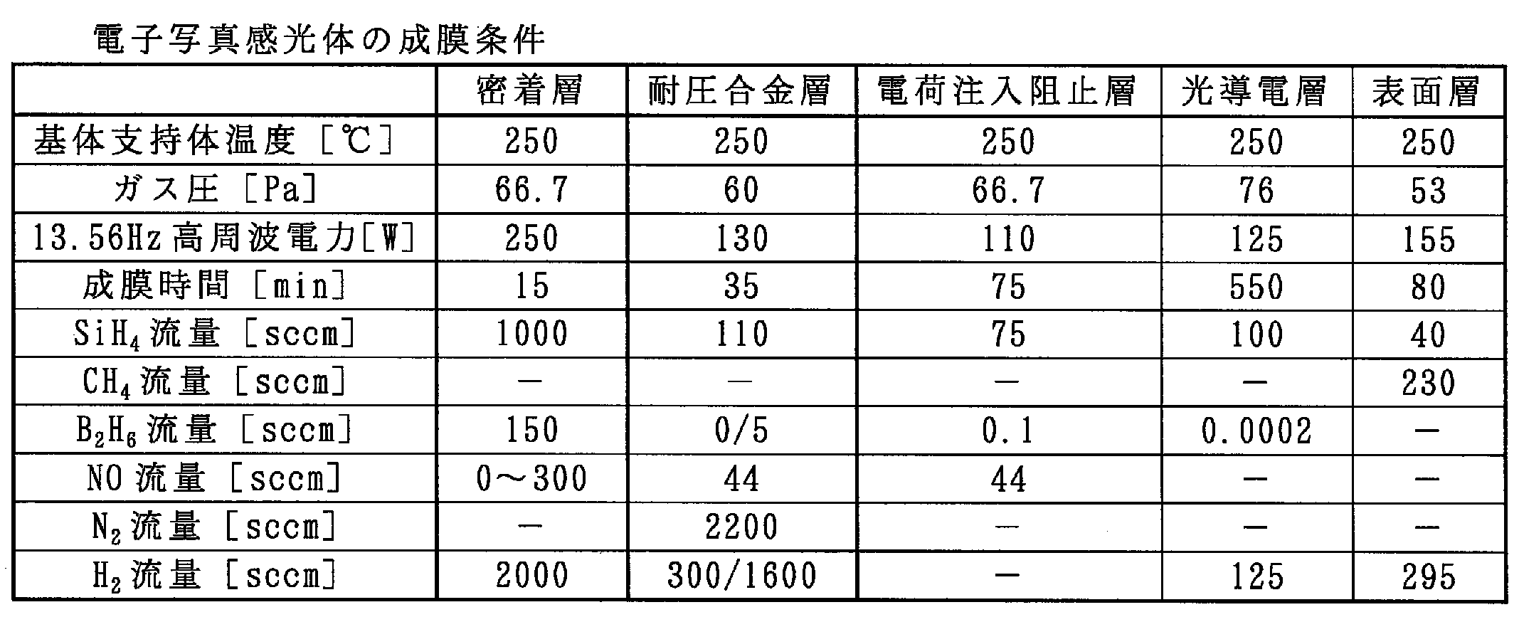
[膜剥がれの発生の有無]
膜剥がれは、目視および光学顕微鏡(「MMFP-TR」;OLYMPAS社製)により確認した。膜剥がれの評価結果については、膜剥がれがないものを「○」、実使用上は問題ない程度の微小な膜剥がれがあるものを「△」、実使用上問題となる程度の膜剥がれが発生しているものを「×」として表3に示した。 [Presence or absence of film peeling]
The film peeling was confirmed visually and with an optical microscope (“MMFP-TR”; manufactured by OLYMPAS). As for the evaluation results of film peeling, “○” indicates that there is no film peeling, “△” indicates that there is no problem in actual use, and “Δ” indicates that there is a problem in actual use. These are shown in Table 3 as “x”.

表3から分かるように、a-SiONB含有層におけるO元素およびN元素の含有量は、原子数を基準としてSi元素を100としたときに、それぞれ1.05%以上および0.630%以上であれば、被覆層の膜剥がれについて、実用上問題ないものであった。とくに、a-SiONB含有層におけるO元素およびN元素の含有量が、それぞれ1.20%以上および0.720%以上のときに、被覆層の膜剥がれが全く発生しないか、ほとんど発生しない結果となった。
As can be seen from Table 3, the contents of O element and N element in the a-SiONB containing layer are 1.05% or more and 0.630% or more, respectively, when the Si element is 100 based on the number of atoms. If so, there was no practical problem with respect to peeling of the coating layer. In particular, when the contents of O element and N element in the a-SiONB containing layer are 1.20% or more and 0.720% or more, respectively, the coating layer does not peel off at all or hardly occurs. became.
したがって、a-SiONB含有層におけるO元素およびN元素の含有量は、被覆層の膜剥がれの発生を抑制する観点からは、原子数を基準としてSi元素を100としたときに、それぞれ1.05%以上および0.630%以上とするのが好ましく、さらに好ましくは、それぞれ1.20%以上および0.720%以上とすればよい。なお、NO/SiH4流量比が0.300を超えると、製造上の爆発発生リスクが高まるため、実質的に製造困難となる。
Therefore, the content of the O element and the N element in the a-SiONB-containing layer is 1.05 when the Si element is 100 based on the number of atoms from the viewpoint of suppressing the occurrence of peeling of the coating layer. % Or more and 0.630% or more, and more preferably 1.20% or more and 0.720% or more, respectively. Note that if the NO / SiH 4 flow rate ratio exceeds 0.300, the risk of explosion in manufacturing increases, so that manufacturing becomes substantially difficult.
本実施例では、a-SiONB含有層におけるB元素の含有量が電気的特性に与える影響を検討した。
In this example, the influence of the B element content in the a-SiONB containing layer on the electrical characteristics was examined.
[電子写真感光体の作成]
電子写真感光体は、基本的に実施例1と同様に表1および表2に示す条件にて作成した。ただし、a-SiONB含有層を形成する場合において、B元素の含有量はa-SiONB含有層を形成するときのB2H6の流量により調整し、NO流量は200sccmに固定した。 [Creation of electrophotographic photoreceptor]
The electrophotographic photoreceptor was prepared under the conditions shown in Tables 1 and 2 basically in the same manner as in Example 1. However, when forming the a-SiONB-containing layer, the content of B element was adjusted by the flow rate of B 2 H 6 when forming the a-SiONB-containing layer, and the NO flow rate was fixed at 200 sccm.
[電気的特性の評価]
電気的特性は、暗部電位および除電後電位として評価した。暗部電位および除電後電位は、電子写真感光体を電位測定機(京セラ株式会社製)に組み込んだ状態で測定した。暗部電位は、電子写真感光体の表面を500Vに帯電させた後の電位として、非接触型表面電位計(「MODEL344」:TREK社製)を用いて測定した。除電後電位は、帯電後の電子写真感光体の表面を除電した後の電位として、接触型表面電位計(「MODEL344」:TREK社製)を用いて測定した。暗部電位および除電後電位の測定結果については、図3に示した。 [Evaluation of electrical characteristics]
Electrical characteristics were evaluated as dark potential and post-static potential. The dark portion potential and the post-static potential were measured in a state where the electrophotographic photosensitive member was incorporated in a potential measuring machine (manufactured by Kyocera Corporation). The dark portion potential was measured as a potential after charging the surface of the electrophotographic photosensitive member to 500 V using a non-contact type surface potential meter (“MODEL 344”: manufactured by TREK). The post-charge potential was measured using a contact type surface potential meter (“MODEL 344”: manufactured by TREK Co., Ltd.) as the potential after the surface of the charged electrophotographic photosensitive member was discharged. The measurement results of the dark part potential and the post-static charge potential are shown in FIG.
図3に示したように、a-SiONB含有層におけるB元素の含有量が大きくなるにつれて暗部電位および除電後電位が大きくなった。実用的に画像形成に問題がない閾値を、暗部電位について500V以上、除電後電位について80V以下と設定すれば、a-SiONB含有層におけるB元素の含有量は、原子数を基準としてSiを元素の含有量を100としたときに200ppm以上1000ppm以下とすればよく、さらに良好な画像を得るためには、Si元素に対するB元素の含有量を350ppm以上700ppm以下に設定すればよいことが分かる。
As shown in FIG. 3, the dark portion potential and the potential after static elimination increased as the B element content in the a-SiONB-containing layer increased. If threshold values that do not cause any problem in image formation are set to 500 V or more for the dark potential and 80 V or less for the potential after static elimination, the content of B element in the a-SiONB-containing layer is determined based on the number of atoms. It is understood that the content of B should be 200 ppm or more and 1000 ppm or less when the content is 100, and in order to obtain a better image, the content of B element with respect to Si element should be set to 350 ppm or more and 700 ppm or less.
本実施例では、a-SiONB含有層の厚みが画像特性に与える影響を検討した。
In this example, the influence of the thickness of the a-SiONB-containing layer on the image characteristics was examined.
[電子写真感光体の作成]
電子写真感光体は、基本的に実施例1と同様に表1および表2に示す条件にて作成した。ただし、a-SiONB含有層を形成する場合において、a-SiONB含有層の厚みは成膜時間により調整し、NO流量は200sccmに固定した。 [Creation of electrophotographic photoreceptor]
The electrophotographic photoreceptor was prepared under the conditions shown in Tables 1 and 2 basically in the same manner as in Example 1. However, when the a-SiONB-containing layer was formed, the thickness of the a-SiONB-containing layer was adjusted by the film formation time, and the NO flow rate was fixed at 200 sccm.
[画像特性の評価]
画像特性は、除電後電位として評価した。除電後電位は、実施例2と同様に測定した。除電後電位の測定結果については、図4に示した。 [Evaluation of image characteristics]
Image characteristics were evaluated as potential after static elimination. The potential after static elimination was measured in the same manner as in Example 2. The measurement results of the potential after static elimination are shown in FIG.
図4に示したように、a-SiONB含有層の厚みが大きくなるにつれて除電後電位が大きくなった。実用的に画像形成に問題がない除電後電位の閾値を80V以下に設定するとすれば、a-SiONB含有層の厚みは、1μm以下に設定すればよいことが分かる。さらに良好な画像を得るためには、a-SiONB含有層の厚みを0.5μm以下に設定すればよい。
As shown in FIG. 4, the potential after static elimination increased as the thickness of the a-SiONB-containing layer increased. Assuming that the threshold value of the post-static potential, which has no practical problem in image formation, is set to 80 V or less, the thickness of the a-SiONB-containing layer may be set to 1 μm or less. In order to obtain a better image, the thickness of the a-SiONB-containing layer may be set to 0.5 μm or less.
本実施例では、グロー放電分解装置を用いてa-SiONB含有層を形成する場合に、高周波電力の大きさが電子写真感光体における膜剥がれの発生および電気特性ムラに与える影響を検討した。
In this example, when the a-SiONB-containing layer was formed using a glow discharge decomposition apparatus, the influence of the magnitude of the high-frequency power on the occurrence of film peeling and the electric characteristic unevenness in the electrophotographic photosensitive member was examined.
[電子写真感光体の作成]
電子写真感光体は、a-SiONB含有層を除いて、実施例1と同様の条件にて作成した。a-SiONB含有層は、高周波電力の大きさ除いて、表4に示した条件で形成した。高周波電力は、表5に示した範囲に設定した。 [Creation of electrophotographic photoreceptor]
The electrophotographic photoreceptor was prepared under the same conditions as in Example 1 except for the a-SiONB-containing layer. The a-SiONB-containing layer was formed under the conditions shown in Table 4 except for the magnitude of the high-frequency power. The high frequency power was set in the range shown in Table 5.

[膜剥がれの発生の有無]
膜剥がれの発生の有無は、実施例1と同様にして検討した。膜剥がれの発生の有無の評価結果は、表5に示した。 [Presence or absence of film peeling]
The presence or absence of film peeling was examined in the same manner as in Example 1. Table 5 shows the evaluation results of the presence or absence of film peeling.
膜剥がれの発生の有無は、実施例1と同様にして検討した。膜剥がれの発生の有無の評価結果は、表5に示した。 [Presence or absence of film peeling]
The presence or absence of film peeling was examined in the same manner as in Example 1. Table 5 shows the evaluation results of the presence or absence of film peeling.
[電気特性ムラ]
電気特性ムラは、電位測定機(京セラ株式会社製)により評価した。電子写真感光体の回転速度は1443.6mm/secとした。電子写真感光体の帯電は、コロナ放電により行なった。このコロナ放電は、グリッド電圧が800V±10Vで、グリッド開効率が95%の帯電器を用いて行なった。電源としては、TREK社製高圧電源「MODEL610E」を用いた。電子写真感光体の露光は、光源としてハロゲンランプ(12V、100W)を連続点灯さるとともに波長720nmの干渉フィルターを用いて行なった。露光エネルギーは1.04μJ/cm2に設定した。除電は、光源として透明フィルター付きLEDユニット(波長660nm、光量600μW/cm2)を用いて行なった。測定時の感光体温度は、42±2℃に設定した。表面電位の値は、TREK社製プローブ「MODEL6000B-7C」を用いて、測定位置は露光後の58°の位置とした。電気特性ムラの評価結果は、表5に示した。 [Electrical characteristics unevenness]
The electrical property unevenness was evaluated by a potential measuring device (manufactured by Kyocera Corporation). The rotational speed of the electrophotographic photosensitive member was 1443.6 mm / sec. The electrophotographic photosensitive member was charged by corona discharge. This corona discharge was performed using a charger having a grid voltage of 800 V ± 10 V and a grid opening efficiency of 95%. As a power source, a high voltage power source “MODEL610E” manufactured by TREK was used. The exposure of the electrophotographic photosensitive member was performed by continuously lighting a halogen lamp (12 V, 100 W) as a light source and using an interference filter having a wavelength of 720 nm. The exposure energy was set to 1.04 μJ / cm 2 . The neutralization was performed using an LED unit with a transparent filter (wavelength: 660 nm, light amount: 600 μW / cm 2 ) as a light source. The photoreceptor temperature at the time of measurement was set to 42 ± 2 ° C. The surface potential was measured using a TREK probe “MODEL6000B-7C”, and the measurement position was 58 ° after exposure. The evaluation results of the electrical characteristic unevenness are shown in Table 5.
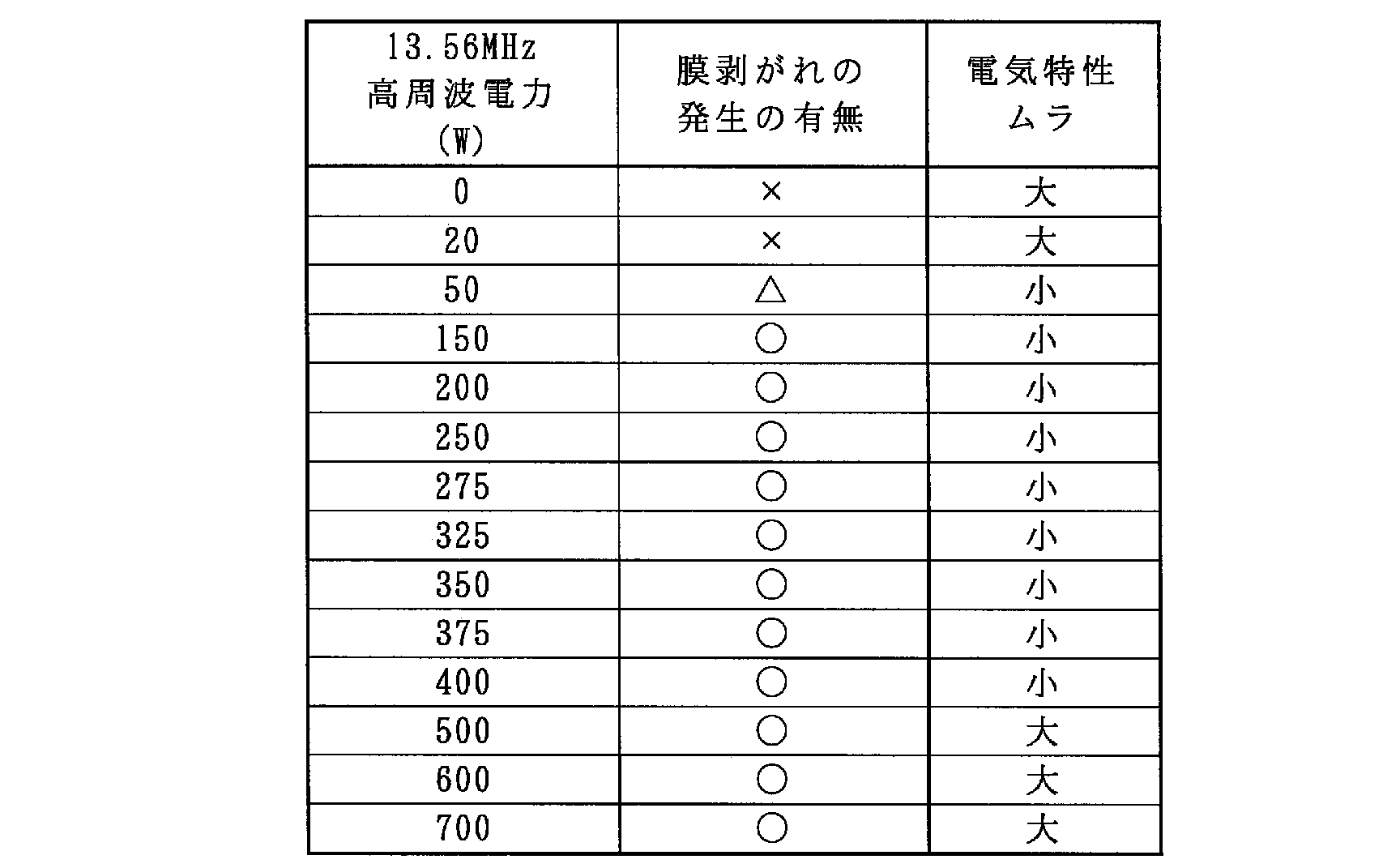
表5から分かるように、被覆層の膜剥がれおよび電気特性ムラの発生を抑制するためには、高周波電力の大きさを50W以上400W以下に設定すればよく、高周波電力の大きさを150W以上400W以下に設定すれば、膜剥がれの発生をより良好に抑制することができる。
As can be seen from Table 5, the magnitude of the high-frequency power may be set to 50 W or more and 400 W or less, and the magnitude of the high-frequency power may be set to 150 W or more and 400 W in order to suppress the peeling of the coating layer and the occurrence of uneven electrical characteristics. If set to the following, the occurrence of film peeling can be suppressed more favorably.
本実施例では、グロー放電分解装置を用いてa-SiONB含有層を形成する場合に、高周波電力1W当たりの原料ガス中のSi流量が電子写真感光体における膜剥がれの発生および解像度に与える影響を検討した。
In this example, when an a-SiONB-containing layer is formed using a glow discharge decomposition apparatus, the influence of the Si flow rate in the source gas per 1 W of high-frequency power on the occurrence of film peeling and resolution on the electrophotographic photoreceptor. investigated.
[電子写真感光体の作成]
電子写真感光体は、a-SiONB含有層を除いて、実施例1と同様の条件にて作成した。a-SiONB含有層は、高周波電力の大きさを除いて、表6に示した条件で形成した。高周波電力は、表7に示した範囲に設定した。 [Creation of electrophotographic photoreceptor]
The electrophotographic photoreceptor was prepared under the same conditions as in Example 1 except for the a-SiONB-containing layer. The a-SiONB-containing layer was formed under the conditions shown in Table 6 except for the magnitude of the high-frequency power. The high frequency power was set in the range shown in Table 7.

[膜剥がれの発生の有無]
膜剥がれの発生の有無は、実施例1と同様にして検討した。膜剥がれの発生の有無の評価結果は、表7に示した。 [Presence or absence of film peeling]
The presence or absence of film peeling was examined in the same manner as in Example 1. Table 7 shows the evaluation results of the presence or absence of film peeling.
膜剥がれの発生の有無は、実施例1と同様にして検討した。膜剥がれの発生の有無の評価結果は、表7に示した。 [Presence or absence of film peeling]
The presence or absence of film peeling was examined in the same manner as in Example 1. Table 7 shows the evaluation results of the presence or absence of film peeling.
[解像度]
解像度は、富士ゼロックス社製「PS5600A」を用いて形成した画像について、qea社製「personal IAS(Image Analysis System)」を用いて、線幅あるいはドットの確認をすることにより評価した。解像度の評価結果については、表7に示した。表7においては、解像度が600dpi以上を「○」とし、解像度が600dpiよりも小さい場合を「×」として示した。 [resolution]
The resolution was evaluated by confirming the line width or dot of an image formed using “PS5600A” manufactured by Fuji Xerox Co., Ltd. using “personal IAS (Image Analysis System)” manufactured by qea. Table 7 shows the resolution evaluation results. In Table 7, “◯” indicates that the resolution is 600 dpi or higher, and “X” indicates that the resolution is smaller than 600 dpi.
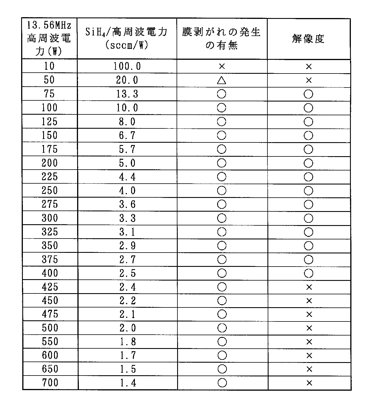
表7から分かるように、被覆層の膜剥がれおよびその他の特性の発生を抑制するためには、高周波電力1W当たりの原料ガス中のSi流量を2.5sccm/W以上13.3sccm/W以下に設定すればよいという結果が得られた。
As can be seen from Table 7, the flow rate of Si in the raw material gas per 1 W of high-frequency power is set to 2.5 sccm / W or more and 13.3 sccm / W or less in order to suppress the peeling of the coating layer and other characteristics. The result that it should just set is obtained.
本実施例では、グロー放電分解装置を用いてa-SiONB含有層を形成する場合に、反応室の圧力が電子写真感光体における膜剥がれの発生および電気特性ムラに与える影響を検討した。
In this example, when the a-SiONB-containing layer was formed using a glow discharge decomposition apparatus, the influence of the pressure in the reaction chamber on the occurrence of film peeling and the electrical property unevenness in the electrophotographic photosensitive member was examined.
[電子写真感光体の作成]
電子写真感光体は、a-SiONB含有層を除いて、実施例1と同様の条件にて作成した。a-SiONB含有層は、圧力を除いて、表8に示した条件で形成した。圧力は、表9に示した範囲に設定した。 [Creation of electrophotographic photoreceptor]
The electrophotographic photoreceptor was prepared under the same conditions as in Example 1 except for the a-SiONB-containing layer. The a-SiONB-containing layer was formed under the conditions shown in Table 8 except for the pressure. The pressure was set in the range shown in Table 9.

[膜剥がれの発生の有無]
膜剥がれの発生の有無は、実施例1と同様にして検討した。膜剥がれの発生の有無の評価結果は、表9に示した。 [Presence or absence of film peeling]
The presence or absence of film peeling was examined in the same manner as in Example 1. Table 9 shows the evaluation results of the presence or absence of film peeling.
膜剥がれの発生の有無は、実施例1と同様にして検討した。膜剥がれの発生の有無の評価結果は、表9に示した。 [Presence or absence of film peeling]
The presence or absence of film peeling was examined in the same manner as in Example 1. Table 9 shows the evaluation results of the presence or absence of film peeling.
[電気特性ムラ]
電気特性ムラは、電位測定機(京セラ株式会社製)を用いて実施例4と同様にして評価した。電気特性ムラの評価結果は、表9に示した。 [Electrical characteristics unevenness]
The electrical property unevenness was evaluated in the same manner as in Example 4 using a potential measuring device (manufactured by Kyocera Corporation). The evaluation results of the electrical characteristic unevenness are shown in Table 9.

表9から分かるように、被覆層の膜剥がれおよび電気特性ムラの発生を抑制するためには、圧力を40Pa以上146.7Pa以下に設定すればよく、圧力を53.3Pa以上133.3Pa以下に設定すれば、膜剥がれの発生をより良好に抑制することができる。
As can be seen from Table 9, the pressure may be set to 40 Pa or more and 146.7 Pa or less, and the pressure may be set to 53.3 Pa or more and 133.3 Pa or less in order to suppress the peeling of the coating layer and the occurrence of uneven electrical characteristics. If set, the occurrence of film peeling can be suppressed more favorably.
本実施例では、グロー放電分解装置を用いてa-SiONB含有層を形成する場合に、成膜時間が電子写真感光体における膜剥がれの発生および電気特性ムラに与える影響を検討した。
In this example, when the a-SiONB-containing layer was formed using a glow discharge decomposition apparatus, the influence of the film formation time on the occurrence of film peeling and the electric characteristic unevenness in the electrophotographic photosensitive member was examined.
[電子写真感光体の作成]
電子写真感光体は、a-SiONB含有層を除いて、実施例1と同様の条件にて作成した。a-SiONB含有層は、成膜時間を除いて、表10に示した条件で形成した。成膜時間は、表11に示した範囲に設定した。 [Creation of electrophotographic photoreceptor]
The electrophotographic photoreceptor was prepared under the same conditions as in Example 1 except for the a-SiONB-containing layer. The a-SiONB-containing layer was formed under the conditions shown in Table 10 except for the film formation time. The film formation time was set in the range shown in Table 11.

[膜剥がれの発生の有無]
膜剥がれの発生の有無は、実施例1と同様にして検討した。膜剥がれの発生の有無の評価結果は、表11に示した。 [Presence or absence of film peeling]
The presence or absence of film peeling was examined in the same manner as in Example 1. Table 11 shows the evaluation results of the presence or absence of film peeling.
膜剥がれの発生の有無は、実施例1と同様にして検討した。膜剥がれの発生の有無の評価結果は、表11に示した。 [Presence or absence of film peeling]
The presence or absence of film peeling was examined in the same manner as in Example 1. Table 11 shows the evaluation results of the presence or absence of film peeling.
[電気特性ムラ]
電気特性ムラは、電位測定機(京セラ株式会社製)を用いて実施例4と同様にして評価した。電気特性ムラの評価結果は、表9に示した。 [Electrical characteristics unevenness]
The electrical property unevenness was evaluated in the same manner as in Example 4 using a potential measuring device (manufactured by Kyocera Corporation). The evaluation results of the electrical characteristic unevenness are shown in Table 9.
電気特性ムラは、電位測定機(京セラ株式会社製)を用いて実施例4と同様にして評価した。電気特性ムラの評価結果は、表9に示した。 [Electrical characteristics unevenness]
The electrical property unevenness was evaluated in the same manner as in Example 4 using a potential measuring device (manufactured by Kyocera Corporation). The evaluation results of the electrical characteristic unevenness are shown in Table 9.

表11から分かるように、被覆層の膜剥がれおよび電気的特性ムラの発生を抑制するためには、成膜時間を3分以上44分以下に設定すればよく、成膜時間を4分以上40分以下に設定すれば、膜剥がれの発生をより良好に抑制することができる。
As can be seen from Table 11, in order to suppress the peeling of the coating layer and the occurrence of uneven electrical characteristics, the film formation time may be set to 3 minutes to 44 minutes, and the film formation time is 4 minutes to 40 minutes. If it is set to less than or equal to minutes, the occurrence of film peeling can be suppressed more favorably.
その一方、本実施例において膜剥がれが適切に抑制されているときのa-SiONB含有層の厚みは、0.15μm以上であり、さらに好ましくは0.20μm以上である。したがって、本実施例の結果から、膜剥がれを抑制するためには、a-SiONB含有層の厚みを0.15μm以上、さらに好ましくは0.20μm以上に設定すればよいことが伺える。
On the other hand, the thickness of the a-SiONB-containing layer when film peeling is appropriately suppressed in this example is 0.15 μm or more, more preferably 0.20 μm or more. Accordingly, it can be seen from the results of this example that the thickness of the a-SiONB-containing layer should be set to 0.15 μm or more, more preferably 0.20 μm or more, in order to suppress film peeling.
Claims (13)
- 導電性基体と、該導電性基体を被覆する被覆層とを備える電子写真感光体であって、
前記被覆層は、感光層と、前記導電性基体と前記感光層との間に位置する耐圧層と、前記導電性基体と前記耐圧層との間に位置するa-SiONB含有層と、を含んでなる、電子写真感光体。 An electrophotographic photosensitive member comprising a conductive substrate and a coating layer covering the conductive substrate,
The covering layer includes a photosensitive layer, a pressure-resistant layer positioned between the conductive substrate and the photosensitive layer, and an a-SiONB-containing layer positioned between the conductive substrate and the pressure-resistant layer. An electrophotographic photoreceptor comprising - 前記a-SiONB含有層におけるN元素の含有量は、原子数を基準として、Si元素の含有量を100としたときに0.630%以上である、請求項1に記載の電子写真感光体。 2. The electrophotographic photosensitive member according to claim 1, wherein the content of N element in the a-SiONB-containing layer is 0.630% or more when the content of Si element is 100 based on the number of atoms.
- 前記a-SiONB含有層におけるO元素の含有量は、原子数を基準として、Si元素の含有量を100としたときに1.05%以上である、請求項1に記載の電子写真感光体。 2. The electrophotographic photosensitive member according to claim 1, wherein the content of O element in the a-SiONB-containing layer is 1.05% or more when the content of Si element is 100, based on the number of atoms.
- 前記a-SiONB含有層におけるB元素の含有量は、Si元素の含有量を100としたときに、200ppm以上1000ppm以下である、請求項1に記載の電子写真感光体。 2. The electrophotographic photoreceptor according to claim 1, wherein the content of B element in the a-SiONB-containing layer is 200 ppm or more and 1000 ppm or less when the content of Si element is 100.
- 前記a-SiONB含有層の厚みは、0.15μm以上1.05μm以下である、請求項1に記載の電子写真感光体。 The electrophotographic photosensitive member according to claim 1, wherein the a-SiONB-containing layer has a thickness of 0.15 µm or more and 1.05 µm or less.
- 前記耐圧層は、a-SiNを含んでいる、請求項1に記載の電子写真感光体。 The electrophotographic photosensitive member according to claim 1, wherein the pressure-resistant layer contains a-SiN.
- 前記耐圧層における窒素原子数とシリコン原子数との合計に対する窒素原子数の比率は、0.01以上0.55以下である、請求項6に記載の電子写真感光体。 The electrophotographic photosensitive member according to claim 6, wherein the ratio of the number of nitrogen atoms to the total number of nitrogen atoms and silicon atoms in the pressure-resistant layer is 0.01 or more and 0.55 or less.
- 前記耐圧層の厚みは、0.5μm以上1.2μm以下である、請求項1に記載の電子写真感光体。 The electrophotographic photosensitive member according to claim 1, wherein the pressure-resistant layer has a thickness of 0.5 μm to 1.2 μm.
- 前記感光層の厚みは、15μm以上90μm以下である、請求項1に記載の電子写真感光体。 The electrophotographic photosensitive member according to claim 1, wherein the photosensitive layer has a thickness of 15 μm or more and 90 μm or less.
- 請求項1に記載の電子写真感光体を備えることを特徴とする、画像形成装置。 An image forming apparatus comprising the electrophotographic photosensitive member according to claim 1.
- 導電性基体上にa-SiONB含有層を形成する第1工程と、前記a-SiONB含有層上に耐圧層を形成する第2工程と、前記耐圧層上に感光層を形成する第3工程と、を含む電子写真感光体の製造方法であって、
前記第1工程は、導電性基体を収容した反応室に原料ガスを供給するとともに、前記導電性基体に高周波電力を供給することにより行なわれ、かつ、
前記高周波電力は、50W以上400W以下に設定される、電子写真感光体の製造方法。 A first step of forming an a-SiONB-containing layer on a conductive substrate, a second step of forming a pressure-resistant layer on the a-SiONB-containing layer, and a third step of forming a photosensitive layer on the pressure-resistant layer. A method for producing an electrophotographic photoreceptor comprising
The first step is performed by supplying a raw material gas to a reaction chamber containing a conductive substrate and supplying high-frequency power to the conductive substrate; and
The method for producing an electrophotographic photosensitive member, wherein the high-frequency power is set to 50 W or more and 400 W or less. - 前記第1工程において、前記原料ガスとしてSi化合物を含有するものが使用され、かつ、前記高周波電力1W当たりの前記Si化合物の流量が2.5sccm以上13.3sccm以下に設定される、請求項11に記載の電子写真感光体の製造方法。 In the first step, a gas containing a Si compound is used as the source gas, and the flow rate of the Si compound per 1 W of the high-frequency power is set to 2.5 sccm or more and 13.3 sccm or less. A process for producing the electrophotographic photosensitive member according to 1.
- 前記第1工程において、前記反応室における圧力が40.0Pa以上146.7Pa以下に設定される、請求項11に記載の電子写真感光体の製造方法。 The method for producing an electrophotographic photosensitive member according to claim 11, wherein, in the first step, the pressure in the reaction chamber is set to 40.0 Pa or more and 146.7 Pa or less.
Priority Applications (1)
| Application Number | Priority Date | Filing Date | Title |
|---|---|---|---|
| JP2009551620A JP5436227B2 (en) | 2008-01-31 | 2009-01-30 | Electrophotographic photoreceptor, image forming apparatus equipped with the same, and method for producing electrophotographic photoreceptor |
Applications Claiming Priority (2)
| Application Number | Priority Date | Filing Date | Title |
|---|---|---|---|
| JP2008022130 | 2008-01-31 | ||
| JP2008-022130 | 2008-01-31 |
Publications (1)
| Publication Number | Publication Date |
|---|---|
| WO2009096552A1 true WO2009096552A1 (en) | 2009-08-06 |
Family
ID=40912895
Family Applications (1)
| Application Number | Title | Priority Date | Filing Date |
|---|---|---|---|
| PCT/JP2009/051637 WO2009096552A1 (en) | 2008-01-31 | 2009-01-30 | Electrophotographic photoreceptor, image-forming device provided with the same, and method for manufacturing an electrophotographic photoreceptor |
Country Status (2)
| Country | Link |
|---|---|
| JP (1) | JP5436227B2 (en) |
| WO (1) | WO2009096552A1 (en) |
Citations (4)
| Publication number | Priority date | Publication date | Assignee | Title |
|---|---|---|---|---|
| JPS59119358A (en) * | 1982-12-27 | 1984-07-10 | Toshiba Corp | Photosensitive body for electrophotography |
| JPS62269147A (en) * | 1986-05-16 | 1987-11-21 | Canon Inc | Light receiving material |
| JPS62276559A (en) * | 1986-05-26 | 1987-12-01 | Canon Inc | Light receiving member |
| JPH0283549A (en) * | 1988-09-20 | 1990-03-23 | Sanyo Electric Co Ltd | Electrostatic latent image carrier |
-
2009
- 2009-01-30 WO PCT/JP2009/051637 patent/WO2009096552A1/en active Application Filing
- 2009-01-30 JP JP2009551620A patent/JP5436227B2/en active Active
Patent Citations (4)
| Publication number | Priority date | Publication date | Assignee | Title |
|---|---|---|---|---|
| JPS59119358A (en) * | 1982-12-27 | 1984-07-10 | Toshiba Corp | Photosensitive body for electrophotography |
| JPS62269147A (en) * | 1986-05-16 | 1987-11-21 | Canon Inc | Light receiving material |
| JPS62276559A (en) * | 1986-05-26 | 1987-12-01 | Canon Inc | Light receiving member |
| JPH0283549A (en) * | 1988-09-20 | 1990-03-23 | Sanyo Electric Co Ltd | Electrostatic latent image carrier |
Also Published As
| Publication number | Publication date |
|---|---|
| JPWO2009096552A1 (en) | 2011-05-26 |
| JP5436227B2 (en) | 2014-03-05 |
Similar Documents
| Publication | Publication Date | Title |
|---|---|---|
| JP4499785B2 (en) | Electrophotographic photoreceptor and image forming apparatus provided with the same | |
| JP4404942B2 (en) | Image forming apparatus | |
| JP4242893B2 (en) | Electrophotographic photoreceptor and image forming apparatus provided with the same | |
| US8055156B2 (en) | Image-forming apparatus which can eliminate static electricity | |
| US8137878B2 (en) | Electrophotographic photoreceptor, method for manufacturing the same, and image-forming apparatus using same | |
| JP4776674B2 (en) | Electrophotographic photoreceptor and image forming apparatus | |
| JP2004077650A (en) | Electrophotographic apparatus | |
| JP4436823B2 (en) | Image forming apparatus | |
| WO2009104466A1 (en) | Electrophotographic photosensitive body and image-forming apparatus comprising the same | |
| JP4242890B2 (en) | Electrophotographic photosensitive member, method for producing the same, and image forming apparatus | |
| JP4996684B2 (en) | Electrophotographic photoreceptor, method for producing the same, and image forming apparatus | |
| JP5436227B2 (en) | Electrophotographic photoreceptor, image forming apparatus equipped with the same, and method for producing electrophotographic photoreceptor | |
| US7672612B2 (en) | Electrophotographic photosensitive member, and image forming apparatus using same | |
| JP2002149029A (en) | Method and apparatus for forming image and photoreceptor | |
| JP4283331B2 (en) | Image forming apparatus | |
| JP5311830B2 (en) | Electrophotographic equipment | |
| JP4273131B2 (en) | Electrophotographic photoreceptor and image forming apparatus provided with the same | |
| WO2020022385A1 (en) | Electrophotographic photoreceptor and image formation device | |
| JP2007293280A (en) | Electrophotographic photosensitive member and image forming apparatus equipped with the same | |
| JP4249751B2 (en) | Image forming apparatus | |
| JPWO2009028448A1 (en) | Electrophotographic photosensitive member and image forming apparatus provided with the electrophotographic photosensitive member | |
| JP2019144476A (en) | Electrophotographic photoreceptor and image forming apparatus including the same | |
| JP2009036932A (en) | Electrophotographic photoreceptor, and image forming apparatus equipped therewith | |
| JPH11212286A (en) | Electrophotographic photoreceptor | |
| JP2009014777A (en) | Inspection method for electrophotographic photoreceptor |
Legal Events
| Date | Code | Title | Description |
|---|---|---|---|
| 121 | Ep: the epo has been informed by wipo that ep was designated in this application |
Ref document number: 09706164 Country of ref document: EP Kind code of ref document: A1 |
|
| WWE | Wipo information: entry into national phase |
Ref document number: 2009551620 Country of ref document: JP |
|
| NENP | Non-entry into the national phase |
Ref country code: DE |
|
| 122 | Ep: pct application non-entry in european phase |
Ref document number: 09706164 Country of ref document: EP Kind code of ref document: A1 |