WO2009087874A1 - Testing apparatus, probe card and testing method - Google Patents
Testing apparatus, probe card and testing method Download PDFInfo
- Publication number
- WO2009087874A1 WO2009087874A1 PCT/JP2008/072967 JP2008072967W WO2009087874A1 WO 2009087874 A1 WO2009087874 A1 WO 2009087874A1 JP 2008072967 W JP2008072967 W JP 2008072967W WO 2009087874 A1 WO2009087874 A1 WO 2009087874A1
- Authority
- WO
- WIPO (PCT)
- Prior art keywords
- test
- signal
- device under
- drivers
- under test
- Prior art date
Links
Images


Classifications
-
- G—PHYSICS
- G01—MEASURING; TESTING
- G01R—MEASURING ELECTRIC VARIABLES; MEASURING MAGNETIC VARIABLES
- G01R31/00—Arrangements for testing electric properties; Arrangements for locating electric faults; Arrangements for electrical testing characterised by what is being tested not provided for elsewhere
- G01R31/28—Testing of electronic circuits, e.g. by signal tracer
- G01R31/317—Testing of digital circuits
- G01R31/3181—Functional testing
- G01R31/319—Tester hardware, i.e. output processing circuits
- G01R31/31917—Stimuli generation or application of test patterns to the device under test [DUT]
- G01R31/31928—Formatter
Definitions
- the present invention relates to a test apparatus, a probe card, and a test method.
- This application is related to the following US applications and claims priority from the following US applications: For designated countries where incorporation by reference of documents is permitted, the contents described in the following application are incorporated into this application by reference and made a part of this application.
- a test apparatus for testing a device under test such as a semiconductor circuit
- an apparatus provided with a plurality of driver comparator pins that exchange signals with the device under test is known.
- a binary test signal can be generated from each driver comparator pin and supplied to the device under test.
- the binary test signal may be a signal having a logic pattern including binary logic values of H logic and L logic, for example.
- FIG. 8 is a diagram illustrating an example of a test apparatus 400 that generates a multi-value test signal.
- the test apparatus 400 includes a pin electronics unit 410 and a probe card 420.
- the pin electronics unit 410 includes a plurality of drivers 412 and a plurality of comparators 414. Each driver 412 outputs a binary test signal.
- the probe card 420 has a plurality of transmission paths 422 and needles 424.
- the plurality of transmission paths 422 are provided in one-to-one correspondence with the plurality of drivers 412.
- Each transmission path 422 transmits a test signal output from the corresponding driver 412.
- the tip of each transmission path 422 is short-circuited in the probe card 420.
- One end of the needle 424 is fixed to each short-circuited transmission path 422 by solder or the like. Further, the other end of the needle 424 contacts a terminal of the device under test and supplies a test signal received via the transmission path 422 to the device under test.
- the plurality of drivers 412 synchronously output the test signals, so that the plurality of test signals are synthesized in the probe card 420, and the multi-value test signals can be supplied to the device under test.
- each driver 412 generates a binary test signal of H logic (1 V) and L logic (0 V).
- the logical value (signal level) of the combined signal is the logical value (0 V) when both drivers 412 output L logic, one driver 412 outputs H logic, and the other driver 412 outputs L logic.
- a multi-value test signal can be generated using a binary driver comparator pin mounted on a conventional test apparatus.
- each driver 412 outputs a test signal at the same time, if the delay amount of each transmission path 422 is different, a multi-value test signal cannot be synthesized accurately.
- TDR Time Domain Reflectometry
- the TDR method is a method for measuring the delay time of a transmission line by inputting a signal to the transmission line with the open end and measuring the delay time of the signal reflected at the front end of the transmission line.
- the comparator 414 since the comparator 414 is connected to the transmission line 422 that is common to the driver 412, the delay of the transmission line 422 is determined from the timing at which the signal is output from the driver 412 and the timing at which the comparator 414 detects the reflected wave. Time can be measured easily.
- the description regarding a prior art document is abbreviate
- the tip of the transmission line 422 is short-circuited and fixed by solder or the like, so that the delay of the transmission line 422 by the TDR method.
- the time cannot be measured. That is, since no reflected wave is generated at the tip of each transmission line 422, the delay time of the transmission line 422 cannot be measured by the TDR method.
- first transmission path 422-1 and the second transmission path 422- 2 are calculated based on the timing at which a signal is output from the first driver 412-1 and the timing at which the second comparator 414-2 detects the signal.
- the sum of delay times in 2 can be measured.
- the delay times of the first transmission path 422-1 and the second transmission path 422-2 cannot be measured, it is difficult to adjust the timing at which each driver 412 outputs a signal. For this reason, it has been difficult to accurately generate a multi-value test signal.
- an object of one aspect of the present invention is to provide a test apparatus, a probe card, and a test method that can solve the above-described problems. This object is achieved by a combination of features described in the independent claims.
- the dependent claims define further advantageous specific examples of the present invention.
- a test apparatus for testing a device under test, wherein a plurality of test signals are synthesized by supplying a test signal output from each to the same terminal of the device under test.
- a plurality of drivers for supplying a multi-value signal to the terminal, and a plurality of drivers are provided in one-to-one correspondence with each of the drivers, and when testing the device under test, each tip is connected to the same terminal in the device under test.
- a plurality of probe pins that are electrically connected to each other so that a signal output from a corresponding driver is supplied to the corresponding terminal of the device under test, and when the device under test is not tested, each tip is electrically open;
- a test apparatus is provided.
- a test apparatus for testing a device under test, a plurality of drivers each outputting a test signal, a pin electronics unit in which a plurality of drivers are formed, and a pin electronics unit A wiring unit that electrically connects the output terminals of a plurality of drivers on the board and generates a multi-value signal in which a plurality of test signals are synthesized, and a multi-value that the wiring unit transmits outside the pin electronics unit And a probe pin that supplies the signal to the device under test.
- a probe card for use in a test apparatus including a plurality of drivers each outputting a test signal, provided in one-to-one correspondence with a plurality of drivers, When testing, when each tip is electrically connected to the same terminal of the device under test, the signal output by the corresponding driver is supplied to the terminal of the device under test, and the device under test is not tested
- a probe card is provided that includes a plurality of probe pins in which the respective tip portions are electrically opened.
- a device under test is used using a test apparatus that includes a plurality of drivers each outputting a test signal and a plurality of probe pins that supply a test signal output from the corresponding driver to the device under test.
- This is a test method for testing a device.
- the tip of each probe pin is opened, the adjustment signal is output to each driver, and the adjustment signal reflected at the tip of the probe pin is measured and measured.
- Based on the results adjust the timing at which each driver outputs the test signal, electrically connect the tip of each probe pin to the same terminal of the device under test, and output the test signal to each driver
- To supply a device under test with a multi-level signal that combines test signals output by multiple drivers. The law provides.
- FIG. 1 is a diagram illustrating a configuration example of a test apparatus 100 according to an embodiment.
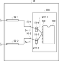
- FIG. 2 is a view showing a probe card 50 together with a device under test 200. An example of the side view which looked at the probe card 50 and the device under test 200 from the position A in FIG. 2 is shown.
- 3 is a diagram illustrating a configuration example of a signal generation unit 12 and a signal processing unit 14.
- FIG. 2 is a flowchart illustrating an operation example of the test apparatus 100. It is a figure which shows the other example of the probe card. It is a figure which shows the other structural example of the pin electronics part 30 and the probe card. It is a figure which shows an example of the test apparatus 400 which produces
- FIG. 1 is a diagram illustrating a configuration example of a test apparatus 100 according to an embodiment.
- the test apparatus 100 tests a device under test such as a semiconductor circuit using a multi-value test signal.
- the test apparatus 100 includes a plurality of signal generation units 12, a plurality of signal processing units 14, a pin electronics unit 30, and a probe card 50.
- the pin electronics unit 30 includes a plurality of drivers 32, a plurality of comparators 34, and a plurality of resistors 36.
- the plurality of drivers 32 are provided in one-to-one correspondence with the plurality of signal generation units 12.
- Each signal generator 12 generates a test signal and supplies it to the corresponding driver 32.
- Each signal generation unit 12 may generate a binary test signal having a logic pattern including binary logic values of H logic and L logic, for example.
- the signal generation unit 12 may generate a voltage waveform that the test signal should have and supply it to the driver 32.
- the driver 32 outputs a voltage corresponding to the received voltage waveform.
- the driver 32 may output a current consumed by the device under test in accordance with the test signal.
- Each driver 32 supplies a test signal to the probe card 50 via the resistor 36.
- the plurality of drivers 32 supply test signals output from the respective terminals to the same terminal of the device under test, thereby supplying a multi-value signal obtained by synthesizing the plurality of test signals to the terminal.
- a plurality of transmission lines 52 and a plurality of probe pins 54 are fixed to the probe card 50.
- the plurality of transmission paths 52 are formed on the probe card 50 in one-to-one correspondence with the plurality of drivers 32.
- the plurality of probe pins 54 are provided in one-to-one correspondence with the plurality of transmission paths 52.
- Each transmission path 52 transmits the signal output from the corresponding driver 32 to the corresponding probe pin 54.
- Each probe pin 54 has a connection portion 56 and a tip portion 58.
- the connecting portion 56 and the tip portion 58 may be both ends of the probe pin 54.
- the connection portion 56 of each probe pin 54 is fixed on the substrate of the probe card 50 and connected to the transmission path 52.
- Each probe pin 54 is electrically connected to the same terminal in the device under test when testing the device under test.
- each probe pin 54 is formed such that the tip portion 58 protrudes from the surface of the probe card 50, and contacts the same terminal of the device under test arranged to face the probe card 50.
- a multi-value signal obtained by synthesizing a plurality of test signals output from the plurality of drivers 32 is supplied to the device under test.
- each probe pin 54 is formed so that each tip 58 is electrically opened when the device under test is not tested. In other words, each probe pin 54 is formed so that the tip 58 is normally open and is electrically connected via the pad of the device under test when testing the device under test.
- the signal output from the driver 32 when the device under test is not tested is reflected at the tip 58 of the probe pin 54.
- the signal reflected at the tip 58 of the probe pin 54 is measured by the corresponding comparator 34.
- the plurality of comparators 34 are provided in one-to-one correspondence with the plurality of drivers 32, and the input ends of the respective comparators 34 are electrically connected to the output ends of the corresponding drivers 32.
- Each comparator 34 measures a response signal output from the device under test when the device under test is tested.
- each comparator 34 measures the adjustment signal output from the driver 32 and the reflected wave thereof.
- Each comparator 34 in this example measures a signal transmitted through a connection point between the resistor 36 and the transmission path 52.
- the comparator 34 receives the adjustment signal output from the driver 32 via the resistor 36 and receives the reflected wave of the adjustment signal via the transmission line 52.
- the comparator 34 is provided in one-to-one correspondence with the driver 32 in one-to-one correspondence with the driver 32 in another example.
- one comparator 34 may be provided for the plurality of drivers 32.
- the comparators 34 are arranged so that the distance (signal transmission time) between the comparator 34 and each driver 32 is sufficiently small to be negligible with respect to the delay time in the transmission path 52.
- the comparator 34 may sequentially measure the adjustment signal output from the driver 32 and the reflected wave thereof for each driver 32.
- the signal processing unit 14 may calculate the delay time in the transmission path 52 based on the elapsed time from when the comparator 34 detects the adjustment signal until the reflected wave of the adjustment signal is detected. For example, the signal processing unit 14 may calculate 1 ⁇ 2 of the elapsed time as the delay time in the transmission path 52. The signal processing unit 14 adjusts the timing at which each driver 32 outputs a test signal based on the delay time in each transmission path 52.
- the device under test can be tested by generating a multi-value test signal of three or more values using the driver 32 that generates a binary signal. Further, the delay time in each transmission path 52 can be easily measured by the TDR method. For this reason, the output timing of the signal in each driver 32 can be easily adjusted, and a multi-value test signal can be generated with high accuracy.
- test apparatus 100 having two drivers 32, two transmission paths 52, and two probe pins 54 will be described. 100 may have a greater number of drivers 32, transmission lines 52, and probe pins 54. Further, the test apparatus 100 may have the same number of other components such as the comparators 34 corresponding thereto. The test apparatus 100 may generate a plurality of multi-value test signals in parallel using these, or may generate a multi-value test signal and a binary test signal in parallel.
- the resistor 36 matches the impedance between the transmission line 52 and the driver 32.
- the resistor 36 may have substantially the same impedance as the transmission line 52.
- the probe card 50 is provided so as to be replaceable with respect to the test apparatus 100.
- the user or the like applies the multi-value test signal of three or more values to the device under test, and the device under test using the binary test signal without using the multi-value test signal.
- the probe card 50 used when testing the above may be prepared in advance. The user or the like may replace the probe card 50 according to the type of test to be performed.
- FIG. 2 is a diagram showing the probe card 50 together with the device under test 200.
- the device under test 200 may be tested in a state where it is formed on a semiconductor wafer on a disk, for example.
- the device under test 200 has a terminal 210. Although one terminal 210 is shown in FIG. 2, the device under test 200 may have a plurality of terminals 210.
- the test apparatus 100 can apply a multi-value test signal to the terminal 210.
- FIG. 3 shows an example of a side view of the probe card 50 and the device under test 200 as seen from the position A in FIG.
- the device under test 200 of this example is arranged to face the probe card 50.
- Each probe pin 54 is formed so as to protrude in the direction of the device under test 200 from the surface of the probe card 50, and contacts a common terminal 210 in the device under test 200.
- the common terminal 210 may have a width that allows contact with the plurality of tip portions 58.
- the width of the common terminal 210 that contacts the plurality of probe pins 54 may be larger than the width of the terminal that contacts one probe pin 54.
- the plurality of probe pins 54 may be formed such that the interval between the tip portions 58 is smaller than the interval between the connection portions 56. Further, the interval between the tip portions 58 may be narrower than the width of the terminal 210 of the device under test 200.
- the intervals between the tip portions 58 of the plurality of probe pins 54 that generate the multi-value test signal may be narrower than the intervals between the tip portions 58 of the plurality of probe pins 54 that generate a plurality of binary test signals in parallel.
- the plurality of probe pins 54 may be arranged in a substantially straight line along an arrangement direction substantially parallel to the terminals of the device under test 200 provided in a substantially straight line. Further, when a plurality of terminals are provided on each side of the device under test 200, the plurality of probe pins 54 may be provided in two rows so as to face each row of terminals.
- the interval in the arrangement direction of the tip portions 58 of some probe pins 54 is the same as that of the tip portions 58 of other probe pins 54.
- a plurality of probe pins 54 may be formed so as to be different from the interval in the arrangement direction. That is, the plurality of probe pins 54 may be formed such that a plurality of types of intervals are mixed as the intervals in the arrangement direction of the tip portions 58 of the plurality of probe pins 54.
- FIG. 4 is a diagram illustrating a configuration example of the signal generation unit 12 and the signal processing unit 14.
- one signal generation unit 12 and one signal processing unit 14 are shown, but each signal generation unit 12 may have the same configuration, and each signal processing unit 14 also has the same configuration. You can do it.
- each signal generation unit 12 includes a pattern generation unit 16, a timing generation unit 20, and a waveform shaping unit 18.
- the pattern generator 16 generates a logical pattern that the test signal and the adjustment signal output from the signal generator 12 should have.
- the pattern generator 16 may generate a binary logic pattern.
- the timing generator 20 generates the timing information of the test signal and the adjustment signal output from the signal generator 12. For example, the timing generator 20 may generate a timing signal that determines the phase (or edge position), period (or bit rate), etc. of the signal.
- the waveform shaping unit 18 generates a test signal and an adjustment signal based on the logic pattern generated by the pattern generation unit 16 and the timing signal generated by the timing generation unit 20.
- the waveform shaping unit 18 may shape the voltage waveform of the signal.
- the waveform shaping unit 18 supplies the generated signal to the driver 32.
- the timing measurement unit 24 receives the signal measured by the comparator 34.
- the comparator 34 of this example outputs a comparison result signal indicating the magnitude relationship between the voltage level of the input signal and the applied reference level VOL as a binary logical value.
- the timing measurement unit 24 sequentially acquires the logical value of the comparison result signal at a timing corresponding to the given strobe signal pulse.
- the signal generator 12 When testing the device under test 200, the signal generator 12 outputs a test signal. For example, the signal generator 12 may output a test signal having a logic pattern determined by a user or the like.
- the comparator 34 receives a response signal output from the device under test 200 in response to the test signal, and the timing measurement unit 24 acquires a logical value pattern of the comparison result signal output from the comparator 34.
- the determination unit 26 determines pass / fail of the device under test 200 based on whether or not the logical value pattern acquired by the timing measurement unit 24 matches a predetermined expected value pattern.
- the signal generator 12 When measuring the delay time of the transmission path 52, the signal generator 12 outputs an adjustment signal. For example, the signal generation unit 12 may output a step signal or one pulse as the adjustment signal.
- the comparator 34 sequentially receives the adjustment signal output from the driver 32 and the reflected wave thereof. In the timing measurement unit 24, the comparator 34 sequentially receives the comparison result signal output for the adjustment signal and the comparison result signal output for the reflected wave, and sequentially acquires the respective logical value patterns.
- the pattern generator 16 and the timing generator 20 When measuring the delay time of the transmission path 52, the pattern generator 16 and the timing generator 20 output a predetermined logic pattern and timing signal so that the driver 32 outputs an adjustment signal.
- the synchronization adjustment unit 22 may instruct that the delay time of the transmission line 52 is measured.
- the synchronization adjustment unit 22 adjusts the timing at which the driver 32 outputs a signal based on the adjustment signal measured by the comparator 34 and the timing measurement unit 24 and the measurement result of the reflected wave. For example, the synchronization adjustment unit 22 may calculate a difference in timing when the comparator 34 detects a corresponding edge in the adjustment signal and the reflected wave based on the measurement result in the timing measurement unit 24. The timing difference corresponds to the delay time of the transmission path 52.
- Each synchronization adjustment unit 22 adjusts the timing at which the corresponding driver 32 outputs a signal based on the delay time of the corresponding transmission line 52. That is, each synchronization adjusting unit 22 is configured so that the test signals applied to the device under test 200 from the respective drivers 32 via the transmission path 52 are applied to the device under test 200 at substantially the same timing. The signal output timing of each driver 32 is adjusted according to the delay time of the transmission path 52.
- each synchronization adjusting unit 22 may adjust the signal output timing of each driver 32 based on the difference in delay time of each transmission path 52 with respect to a predetermined reference delay time. As the reference delay time, the delay time of any one of the transmission paths 52 may be used. In addition, the synchronization adjustment unit 22 may adjust the signal output timing of the driver 32 by adjusting the phase of the timing signal output from the timing generation unit 20.
- the signal output timing in each driver 32 can be adjusted to synthesize a multi-value test signal with high accuracy. For this reason, the device under test 200 can be tested with high accuracy.
- FIG. 5 shows a flowchart for explaining an operation example of the test apparatus 100.
- the test apparatus 100 adjusts the signal output timing of each driver 32 before testing the device under test 200.
- the device under test 200 is not brought into contact with the probe pin 54, and the tip portions 58 of the plurality of probe pins 54 used for generating the multi-value signal are respectively opened (S300).
- an adjustment signal is output from each driver 32 (S302).
- each synchronization adjustment unit 22 may calculate the delay time of each transmission path 52 from the timing difference at which each comparator 34 detects the adjustment signal and the reflected wave.
- each synchronization adjustment unit 22 adjusts the signal output timing in each driver 32 based on the calculated delay time (S308).
- the device under test 200 After adjusting the driver 32, the device under test 200 is arranged at a position facing the probe card 50, and the tip portion 58 of each probe pin 54 that generates a multilevel signal is brought into contact with the same terminal of the device under test 200. (S310). Then, a test signal is output from each driver 32 to test the device under test 200 (S312). With such an operation, the device under test 200 can be tested by generating a multilevel signal with high accuracy.
- FIG. 6 is a diagram illustrating another example of the probe card 50.
- the probe card 50 in this example includes a plurality of transmission paths 52 and a plurality of probe pins 54, similarly to the probe card 50 described with reference to FIGS.
- each probe pin 54 makes a one-to-one contact with each terminal 210 of the device under test 200.
- the terminal 210 may be an electrode formed on a semiconductor wafer.
- Each terminal 210 is connected to a common input pin 230 in the circuit section 220 of the device under test 200.
- FIG. 7 is a diagram illustrating another configuration example of the pin electronics unit 30 and the probe card 50.
- the pin electronics unit 30 of this example includes a plurality of drivers 32, a plurality of comparators 34, and a wiring unit 42.
- the plurality of drivers 32 and the plurality of comparators 34 may be the same as the driver 32 and the plurality of comparators 34 described with reference to FIGS.
- the wiring unit 42 electrically connects the output terminals of the plurality of drivers 32 on the substrate of the pin electronics unit 30 to generate a multi-value signal in which a plurality of test signals are synthesized.
- the wiring unit 42 includes a plurality of resistors 36, a common resistor 38, and a common transmission path 40.
- the plurality of resistors 36 may be the same as the plurality of resistors 36 described in connection with FIGS.
- the common resistor 38 is connected to a plurality of resistors 36.
- One end of the common transmission path 40 is electrically connected to the probe card 50, and the other end is electrically connected to the output end of each driver 32 via the common resistor 38.
- the common transmission path 40 may be provided so that signal delay times from the output ends of the respective drivers 32 to the common transmission path 40 are substantially equal. More specifically, the common transmission line 40 is preferably provided in the vicinity of each driver 32 so that the signal delay time from the output end of each driver 32 to the common transmission line 40 can be regarded as almost zero. .
- the common resistor 38 matches the impedance between the resistor 36 provided at the output of each driver 32 and the common transmission path 40.
- the impedance of the common resistor 38 may be half of the impedance of each resistor 36.
- the probe card 50 has a probe pin 54.
- the probe pin 54 may be the same as the probe pin 54 described in connection with FIGS.
- the probe pin 54 receives the multi-value test signal transmitted by the common transmission path 40 outside the substrate of the pin electronics unit 30 and supplies it to the device under test 200. Note that the probe pins 54 of this example are in one-to-one contact with the terminals 210 of the device under test 200.
- the test apparatus 100 of this example since the signal delay time from each driver 32 to the common transmission path 40 is substantially zero, if the test signals are simultaneously output from each driver 32, the multi-value test signal is accurately obtained. Can be generated well. Further, the common resistor 38 and the common transmission path 40 may be formed in the probe card 50.
- a device under test can be tested by generating a multi-value test signal of three or more values using a driver that generates a binary signal.
- the delay time in each transmission path can be easily measured by the TDR method. For this reason, the output timing of the signal in each driver can be easily adjusted, and a multi-value test signal can be generated with high accuracy.
Abstract
Provided is a testing apparatus for testing a device to be tested. The testing apparatus is provided with a plurality of drivers, which supply a multiple-value signal, wherein a plurality of test signals are synthesized, to a same terminal of the device to be tested, by supplying test signals outputted from respective drivers to the same terminal. The testing apparatus is also provided with a plurality of probe pins, which are arranged one by one for the drivers and electrically connected to the same terminal of the device to be tested at each leading end section, and supply the signals outputted from the corresponding drivers to the terminal of the device to be tested, and permits each leading end section to be in electrically opened state when not testing the device.
Description
本発明は、試験装置、プローブカード、および試験方法に関する。本出願は、下記の米国出願に関連し、下記の米国出願からの優先権を主張する出願である。文献の参照による組み込みが認められる指定国については、下記の出願に記載された内容を参照により本出願に組み込み、本出願の一部とする。
出願番号11/971,207 出願日 2008年1月8日 The present invention relates to a test apparatus, a probe card, and a test method. This application is related to the following US applications and claims priority from the following US applications: For designated countries where incorporation by reference of documents is permitted, the contents described in the following application are incorporated into this application by reference and made a part of this application.
Application No. 11 / 971,207 Application Date January 8, 2008
従来、半導体回路等の被試験デバイスを試験する試験装置において、被試験デバイスとの間で信号を受け渡すドライバコンパレータピンを複数備える装置が知られている。被試験デバイスに試験信号を供給する場合、それぞれのドライバコンパレータピンからは、2値の試験信号を生成して被試験デバイスに供給することができる。2値の試験信号とは、例えばH論理およびL論理の2値の論理値を含む論理パターンを有する信号であってよい。
2. Description of the Related Art Conventionally, in a test apparatus for testing a device under test such as a semiconductor circuit, an apparatus provided with a plurality of driver comparator pins that exchange signals with the device under test is known. When supplying a test signal to the device under test, a binary test signal can be generated from each driver comparator pin and supplied to the device under test. The binary test signal may be a signal having a logic pattern including binary logic values of H logic and L logic, for example.
また、被試験デバイスの試験において、被試験デバイスに3値以上の多値の試験信号を供給したい場合がある。このような場合、多値の試験信号を生成できるドライバコンパレータピンを試験装置に新たに追加することも考えられるが、コストが上昇してしまう。このため、既に実装されている2値のドライバコンパレータピンを用いて、多値の試験信号を生成することが考えられる。
Also, when testing a device under test, it may be desired to supply a multi-value test signal of three or more values to the device under test. In such a case, it may be possible to newly add a driver comparator pin capable of generating a multi-value test signal to the test apparatus, but the cost increases. For this reason, it is conceivable to generate a multi-value test signal using a binary driver comparator pin that is already mounted.
図8は、多値の試験信号を生成する試験装置400の一例を示す図である。試験装置400は、ピンエレクトロニクス部410およびプローブカード420を備える。ピンエレクトロニクス部410は、複数のドライバ412および複数のコンパレータ414を有する。それぞれのドライバ412は、それぞれ2値の試験信号を出力する。
FIG. 8 is a diagram illustrating an example of a test apparatus 400 that generates a multi-value test signal. The test apparatus 400 includes a pin electronics unit 410 and a probe card 420. The pin electronics unit 410 includes a plurality of drivers 412 and a plurality of comparators 414. Each driver 412 outputs a binary test signal.
プローブカード420は、複数の伝送路422およびニードル424を有する。複数の伝送路422は、複数のドライバ412と一対一に対応して設けられる。それぞれの伝送路422は、対応するドライバ412が出力する試験信号を伝送する。また、それぞれの伝送路422の先端は、プローブカード420において短絡される。
The probe card 420 has a plurality of transmission paths 422 and needles 424. The plurality of transmission paths 422 are provided in one-to-one correspondence with the plurality of drivers 412. Each transmission path 422 transmits a test signal output from the corresponding driver 412. In addition, the tip of each transmission path 422 is short-circuited in the probe card 420.
ニードル424は、短絡されたそれぞれの伝送路422に、半田等により一端が固定される。また、ニードル424の他端は、被試験デバイスの端子に接触して、伝送路422を介して受け取る試験信号を、被試験デバイスに供給する。このとき、複数のドライバ412が同期して試験信号を出力することで、プローブカード420において複数の試験信号が合成され、多値の試験信号を被試験デバイスに供給することができる。
One end of the needle 424 is fixed to each short-circuited transmission path 422 by solder or the like. Further, the other end of the needle 424 contacts a terminal of the device under test and supplies a test signal received via the transmission path 422 to the device under test. At this time, the plurality of drivers 412 synchronously output the test signals, so that the plurality of test signals are synthesized in the probe card 420, and the multi-value test signals can be supplied to the device under test.
例えば、それぞれのドライバ412が、H論理(1V)およびL論理(0V)の2値の試験信号を生成する場合を考える。また、2つのドライバ412の出力を短絡して多値の試験信号を生成する場合を考える。この場合の合成信号の論理値(信号レベル)は、2つのドライバ412が共にL論理を出力したときの論理値(0V)、一方のドライバ412がH論理、他方のドライバ412がL論理を出力したときの論理値(0.5V)、および、2つのドライバ412が共にH論理を出力したときの論理値(1V)の3つの論理値を取りうる。
For example, consider a case where each driver 412 generates a binary test signal of H logic (1 V) and L logic (0 V). Consider a case where the outputs of the two drivers 412 are short-circuited to generate a multi-value test signal. In this case, the logical value (signal level) of the combined signal is the logical value (0 V) when both drivers 412 output L logic, one driver 412 outputs H logic, and the other driver 412 outputs L logic. The logic value (0.5V) when the two drivers 412 output H logic, and the logic value (1V) when the two drivers 412 output H logic.
このような構成により、従来の試験装置に実装されている2値のドライバコンパレータピンを用いて、多値の試験信号を生成することができる。ただし、それぞれのドライバ412が同時に試験信号を出力しても、それぞれの伝送路422の遅延量が異なると、多値の試験信号を精度よく合成することができない。
With such a configuration, a multi-value test signal can be generated using a binary driver comparator pin mounted on a conventional test apparatus. However, even if each driver 412 outputs a test signal at the same time, if the delay amount of each transmission path 422 is different, a multi-value test signal cannot be synthesized accurately.
このため、それぞれの伝送路422の遅延量を予め測定して、それぞれの伝送路422の遅延量に応じて、それぞれのドライバ412が試験信号を出力するタイミングを調整することが好ましい。ここで、伝送路422の遅延量を測定する方法として、TDR(Time Domain Reflectometry)法が知られている。
For this reason, it is preferable to measure the delay amount of each transmission path 422 in advance and adjust the timing at which each driver 412 outputs a test signal according to the delay amount of each transmission path 422. Here, as a method of measuring the delay amount of the transmission path 422, a TDR (Time Domain Reflectometry) method is known.
TDR法は、先端が開放状態の伝送路に信号を入力して、伝送路の先端において反射された信号の遅延時間を測定することで、伝送路の遅延時間を測定する方法である。試験装置400では、コンパレータ414が、ドライバ412と共通の伝送路422に接続されるので、ドライバ412から信号を出力したタイミングと、コンパレータ414が反射波を検出するタイミングとから、伝送路422の遅延時間を容易に測定することができる。なお、現時点で先行技術文献の存在を認識していないので、先行技術文献に関する記載を省略する。
The TDR method is a method for measuring the delay time of a transmission line by inputting a signal to the transmission line with the open end and measuring the delay time of the signal reflected at the front end of the transmission line. In the test apparatus 400, since the comparator 414 is connected to the transmission line 422 that is common to the driver 412, the delay of the transmission line 422 is determined from the timing at which the signal is output from the driver 412 and the timing at which the comparator 414 detects the reflected wave. Time can be measured easily. In addition, since the presence of a prior art document is not recognized at this time, the description regarding a prior art document is abbreviate | omitted.
しかし、図8に示したように、多値の試験信号を生成する試験装置400においては、伝送路422の先端が短絡され、半田等により固定されているので、TDR法により伝送路422の遅延時間を測定することができない。つまり、それぞれの伝送路422の先端において反射波が生じないので、TDR法では伝送路422の遅延時間を測定することができない。
However, as shown in FIG. 8, in the test apparatus 400 that generates a multi-value test signal, the tip of the transmission line 422 is short-circuited and fixed by solder or the like, so that the delay of the transmission line 422 by the TDR method. The time cannot be measured. That is, since no reflected wave is generated at the tip of each transmission line 422, the delay time of the transmission line 422 cannot be measured by the TDR method.
なお、第1のドライバ412-1から信号を出力するタイミングと、第2のコンパレータ414-2が当該信号を検出するタイミングとから、第1の伝送路422-1および第2の伝送路422-2における遅延時間の和を測定することはできる。しかし、第1の伝送路422-1および第2の伝送路422-2のそれぞれの遅延時間を測定することはできないので、それぞれのドライバ412が信号を出力するタイミングを調整することは難しい。このため、多値の試験信号を精度よく生成することが困難であった。
Note that the first transmission path 422-1 and the second transmission path 422- 2 are calculated based on the timing at which a signal is output from the first driver 412-1 and the timing at which the second comparator 414-2 detects the signal. The sum of delay times in 2 can be measured. However, since the delay times of the first transmission path 422-1 and the second transmission path 422-2 cannot be measured, it is difficult to adjust the timing at which each driver 412 outputs a signal. For this reason, it has been difficult to accurately generate a multi-value test signal.
そこで本発明の1つの側面においては、上記の課題を解決することのできる試験装置、プローブカード、および試験方法を提供することを目的とする。この目的は請求の範囲における独立項に記載の特徴の組み合わせにより達成される。また従属項は本発明の更なる有利な具体例を規定する。
Therefore, an object of one aspect of the present invention is to provide a test apparatus, a probe card, and a test method that can solve the above-described problems. This object is achieved by a combination of features described in the independent claims. The dependent claims define further advantageous specific examples of the present invention.
本発明の第1の態様においては、被試験デバイスを試験する試験装置であって、それぞれが出力する試験信号を被試験デバイスの同一の端子に供給することで、複数の試験信号が合成された多値の信号を当該端子に供給する複数のドライバと、複数のドライバと一対一に対応して設けられ、被試験デバイスを試験するときに、それぞれの先端部が被試験デバイスにおける同一の端子に電気的に接続されて、対応するドライバが出力する信号を被試験デバイスの当該端子に供給し、被試験デバイスを試験しないときに、それぞれの先端部が電気的に開放状態となる複数のプローブピンとを備える試験装置を提供する。
In the first aspect of the present invention, a test apparatus for testing a device under test, wherein a plurality of test signals are synthesized by supplying a test signal output from each to the same terminal of the device under test. A plurality of drivers for supplying a multi-value signal to the terminal, and a plurality of drivers are provided in one-to-one correspondence with each of the drivers, and when testing the device under test, each tip is connected to the same terminal in the device under test. A plurality of probe pins that are electrically connected to each other so that a signal output from a corresponding driver is supplied to the corresponding terminal of the device under test, and when the device under test is not tested, each tip is electrically open; A test apparatus is provided.
本発明の第2の態様においては、被試験デバイスを試験する試験装置であって、それぞれが試験信号を出力する複数のドライバと、複数のドライバが形成されるピンエレクトロニクス部と、ピンエレクトロニクス部の基板上で、複数のドライバの出力端を電気的に接続し、複数の試験信号が合成された多値の信号を生成する配線部と、ピンエレクトロニクス部の外部において、配線部が伝送する多値の信号を受け取り、被試験デバイスに供給するプローブピンとを備える試験装置を提供する。
According to a second aspect of the present invention, there is provided a test apparatus for testing a device under test, a plurality of drivers each outputting a test signal, a pin electronics unit in which a plurality of drivers are formed, and a pin electronics unit A wiring unit that electrically connects the output terminals of a plurality of drivers on the board and generates a multi-value signal in which a plurality of test signals are synthesized, and a multi-value that the wiring unit transmits outside the pin electronics unit And a probe pin that supplies the signal to the device under test.
本発明の第3の形態においては、それぞれが試験信号を出力する複数のドライバを備える試験装置に用いられるプローブカードであって、複数のドライバと一対一に対応して設けられ、被試験デバイスを試験するときに、それぞれの先端部が被試験デバイスにおける同一の端子に電気的に接続されて、対応するドライバが出力する信号を被試験デバイスの当該端子に供給し、被試験デバイスを試験しないときに、それぞれの先端部が電気的に開放状態となる複数のプローブピンを備えるプローブカードを提供する。
According to a third aspect of the present invention, there is provided a probe card for use in a test apparatus including a plurality of drivers each outputting a test signal, provided in one-to-one correspondence with a plurality of drivers, When testing, when each tip is electrically connected to the same terminal of the device under test, the signal output by the corresponding driver is supplied to the terminal of the device under test, and the device under test is not tested In addition, a probe card is provided that includes a plurality of probe pins in which the respective tip portions are electrically opened.
本発明の第4の形態においては、それぞれが試験信号を出力する複数のドライバと、対応するドライバが出力する試験信号を被試験デバイスに供給する複数のプローブピンとを備える試験装置を用いて被試験デバイスを試験する試験方法であって、それぞれのプローブピンの先端部を開放状態として、それぞれのドライバに調整用信号を出力させ、プローブピンの先端部において反射された調整用信号を測定し、測定結果に基づいてそれぞれのドライバが試験信号を出力するタイミングを調整し、それぞれのプローブピンの先端部を、被試験デバイスの同一の端子に電気的に接続させて、それぞれのドライバに試験信号を出力させることにより、複数のドライバが出力する試験信号を合成した多値の信号を、被試験デバイスに供給する試験方法を提供する。
In the fourth aspect of the present invention, a device under test is used using a test apparatus that includes a plurality of drivers each outputting a test signal and a plurality of probe pins that supply a test signal output from the corresponding driver to the device under test. This is a test method for testing a device. The tip of each probe pin is opened, the adjustment signal is output to each driver, and the adjustment signal reflected at the tip of the probe pin is measured and measured. Based on the results, adjust the timing at which each driver outputs the test signal, electrically connect the tip of each probe pin to the same terminal of the device under test, and output the test signal to each driver To supply a device under test with a multi-level signal that combines test signals output by multiple drivers. The law provides.
なお、上記の発明の概要は、本発明の必要な特徴の全てを列挙したものではなく、これらの特徴群のサブコンビネーションもまた、発明となりうる。
Note that the above summary of the invention does not enumerate all the necessary features of the present invention, and sub-combinations of these feature groups can also be the invention.
12・・・信号生成部、14・・・信号処理部、16・・・パターン発生部、18・・・波形成形部、20・・・タイミング発生部、22・・・同期調整部、24・・・タイミング測定部、26・・・判定部、30・・・ピンエレクトロニクス部、32・・・ドライバ、34・・・コンパレータ、36・・・抵抗、38・・・共通抵抗、40・・・共通伝送路、42・・・配線部、50・・・プローブカード、52・・・伝送路、54・・・プローブピン、56・・・接続部、58・・・先端部、100・・・試験装置、200・・・被試験デバイス、210・・・端子、220・・・回路部、230・・・入力ピン、400・・・試験装置、410・・・ピンエレクトロニクス部、412・・・ドライバ、414・・・コンパレータ、420・・・プローブカード、422・・・伝送路、424・・・ニードル
DESCRIPTION OF SYMBOLS 12 ... Signal generation part, 14 ... Signal processing part, 16 ... Pattern generation part, 18 ... Waveform shaping part, 20 ... Timing generation part, 22 ... Synchronization adjustment part, 24. ..Timing measurement unit, 26 ... determination unit, 30 ... pin electronics unit, 32 ... driver, 34 ... comparator, 36 ... resistance, 38 ... common resistance, 40 ... Common transmission path 42... Wiring section 50... Probe card 52. Transmission path 54. Probe pin 56. Connection section 58. Test apparatus 200 ... Device under test 210 ... Terminal 220 ... Circuit part 230 ... Input pin 400 ... Test apparatus 410 ... Pin electronics part 412 ... Driver, 414... Comparator, 42 ... probe card, 422 ... transmission line, 424 ... needle
以下、発明の実施の形態を通じて本発明の(一)側面を説明するが、以下の実施形態は請求の範囲にかかる発明を限定するものではなく、また実施形態の中で説明されている特徴の組み合わせの全てが発明の解決手段に必須であるとは限らない。
Hereinafter, the (1) aspect of the present invention will be described through embodiments of the invention. However, the following embodiments do not limit the invention according to the scope of claims, and the features described in the embodiments are as follows. Not all combinations are essential for the solution of the invention.
図1は、一つの実施形態に係る試験装置100の構成例を示す図である。試験装置100は、多値の試験信号を用いて半導体回路等の被試験デバイスを試験する。試験装置100は、複数の信号生成部12、複数の信号処理部14、ピンエレクトロニクス部30、および、プローブカード50を備える。
FIG. 1 is a diagram illustrating a configuration example of a test apparatus 100 according to an embodiment. The test apparatus 100 tests a device under test such as a semiconductor circuit using a multi-value test signal. The test apparatus 100 includes a plurality of signal generation units 12, a plurality of signal processing units 14, a pin electronics unit 30, and a probe card 50.
ピンエレクトロニクス部30は、複数のドライバ32、複数のコンパレータ34、および、複数の抵抗36を有する。複数のドライバ32は、複数の信号生成部12と一対一に対応して設けられる。
The pin electronics unit 30 includes a plurality of drivers 32, a plurality of comparators 34, and a plurality of resistors 36. The plurality of drivers 32 are provided in one-to-one correspondence with the plurality of signal generation units 12.
それぞれの信号生成部12は試験信号を生成して、対応するドライバ32に供給する。それぞれの信号生成部12は、例えばH論理およびL論理の2値の論理値を含む論理パターンを有する、2値の試験信号を生成してよい。
Each signal generator 12 generates a test signal and supplies it to the corresponding driver 32. Each signal generation unit 12 may generate a binary test signal having a logic pattern including binary logic values of H logic and L logic, for example.
また、信号生成部12は、試験信号が有するべき電圧波形を生成してドライバ32に供給してよい。ドライバ32は、受け取った電圧波形に応じた電圧を出力する。また、ドライバ32は、当該試験信号に応じて被試験デバイスが消費する電流を出力してよい。
Further, the signal generation unit 12 may generate a voltage waveform that the test signal should have and supply it to the driver 32. The driver 32 outputs a voltage corresponding to the received voltage waveform. The driver 32 may output a current consumed by the device under test in accordance with the test signal.
それぞれのドライバ32は、試験信号を、抵抗36を介してプローブカード50に供給する。本例において複数のドライバ32は、それぞれが出力する試験信号を被試験デバイスの同一の端子に供給することで、複数の試験信号が合成された多値の信号を当該端子に供給する。
Each driver 32 supplies a test signal to the probe card 50 via the resistor 36. In this example, the plurality of drivers 32 supply test signals output from the respective terminals to the same terminal of the device under test, thereby supplying a multi-value signal obtained by synthesizing the plurality of test signals to the terminal.
プローブカード50には、複数の伝送路52および複数のプローブピン54が固定される。複数の伝送路52は、複数のドライバ32と一対一に対応して、プローブカード50上に形成される。また、複数のプローブピン54は、複数の伝送路52と一対一に対応して設けられる。それぞれの伝送路52は、対応するドライバ32が出力する信号を、対応するプローブピン54に伝送する。
A plurality of transmission lines 52 and a plurality of probe pins 54 are fixed to the probe card 50. The plurality of transmission paths 52 are formed on the probe card 50 in one-to-one correspondence with the plurality of drivers 32. The plurality of probe pins 54 are provided in one-to-one correspondence with the plurality of transmission paths 52. Each transmission path 52 transmits the signal output from the corresponding driver 32 to the corresponding probe pin 54.
それぞれのプローブピン54は、接続部56および先端部58を有する。接続部56および先端部58は、プローブピン54の両端であってよい。それぞれのプローブピン54の接続部56は、プローブカード50の基板上に固定され、伝送路52と接続される。
Each probe pin 54 has a connection portion 56 and a tip portion 58. The connecting portion 56 and the tip portion 58 may be both ends of the probe pin 54. The connection portion 56 of each probe pin 54 is fixed on the substrate of the probe card 50 and connected to the transmission path 52.
それぞれのプローブピン54は、被試験デバイスを試験するときに、それぞれの先端部58が被試験デバイスにおける同一の端子に電気的に接続される。例えばそれぞれのプローブピン54は、先端部58がプローブカード50の表面から突出するように形成され、プローブカード50と対向して配置される被試験デバイスの同一の端子と接触する。これにより、複数のドライバ32が出力した複数の試験信号を合成した多値の信号を、被試験デバイスに供給する。
Each probe pin 54 is electrically connected to the same terminal in the device under test when testing the device under test. For example, each probe pin 54 is formed such that the tip portion 58 protrudes from the surface of the probe card 50, and contacts the same terminal of the device under test arranged to face the probe card 50. Thus, a multi-value signal obtained by synthesizing a plurality of test signals output from the plurality of drivers 32 is supplied to the device under test.
また、それぞれのプローブピン54は、被試験デバイスを試験しないときには、それぞれの先端部58が電気的に開放状態となるように形成される。つまり、それぞれのプローブピン54は、通常時には先端部58がそれぞれ開放状態であり、被試験デバイスの試験時には、被試験デバイスのパッド等を介して電気的に接続されるように形成される。
Further, each probe pin 54 is formed so that each tip 58 is electrically opened when the device under test is not tested. In other words, each probe pin 54 is formed so that the tip 58 is normally open and is electrically connected via the pad of the device under test when testing the device under test.
これにより、被試験デバイスを試験しないときにドライバ32が出力する信号は、プローブピン54の先端部58において反射される。プローブピン54の先端部58において反射された信号は、対応するコンパレータ34により測定される。
Thereby, the signal output from the driver 32 when the device under test is not tested is reflected at the tip 58 of the probe pin 54. The signal reflected at the tip 58 of the probe pin 54 is measured by the corresponding comparator 34.
複数のコンパレータ34は、複数のドライバ32と一対一に対応して設けられ、それぞれのコンパレータ34の入力端が、対応するドライバ32の出力端と電気的に接続される。それぞれのコンパレータ34は、被試験デバイスを試験する場合、被試験デバイスが出力する応答信号を測定する。また、伝送路52における遅延時間を測定する場合、それぞれのコンパレータ34は、ドライバ32が出力する調整用信号、および、その反射波を測定する。
The plurality of comparators 34 are provided in one-to-one correspondence with the plurality of drivers 32, and the input ends of the respective comparators 34 are electrically connected to the output ends of the corresponding drivers 32. Each comparator 34 measures a response signal output from the device under test when the device under test is tested. When measuring the delay time in the transmission line 52, each comparator 34 measures the adjustment signal output from the driver 32 and the reflected wave thereof.
本例におけるそれぞれのコンパレータ34は、抵抗36と伝送路52との接続点を伝送する信号を測定する。伝送路52における遅延時間を測定する場合、コンパレータ34は、ドライバ32が出力する調整用信号を抵抗36を介して受け取り、調整用信号の反射波を伝送路52を介して受け取る。
Each comparator 34 in this example measures a signal transmitted through a connection point between the resistor 36 and the transmission path 52. When measuring the delay time in the transmission line 52, the comparator 34 receives the adjustment signal output from the driver 32 via the resistor 36 and receives the reflected wave of the adjustment signal via the transmission line 52.
なお、本例では、コンパレータ34をドライバ32と一対一に対応して設けた例を説明したが、他の例では、コンパレータ34は、複数のドライバ32に対して一つ設けられてもよい。この場合、コンパレータ34と、それぞれのドライバ32との距離(信号伝送時間)が、伝送路52における遅延時間に対して無視できる程度に十分小さくなるようにコンパレータ34を配置する。コンパレータ34は、ドライバ32が出力する調整用信号、および、その反射波を、ドライバ32毎に順次測定してよい。
In this example, the example in which the comparator 34 is provided in one-to-one correspondence with the driver 32 has been described. However, in another example, one comparator 34 may be provided for the plurality of drivers 32. In this case, the comparators 34 are arranged so that the distance (signal transmission time) between the comparator 34 and each driver 32 is sufficiently small to be negligible with respect to the delay time in the transmission path 52. The comparator 34 may sequentially measure the adjustment signal output from the driver 32 and the reflected wave thereof for each driver 32.
信号処理部14は、コンパレータ34が、調整用信号を検出してから、調整用信号の反射波を検出するまでの経過時間に基づいて、伝送路52における遅延時間を算出してよい。例えば信号処理部14は、当該経過時間の1/2を、伝送路52における遅延時間として算出してよい。信号処理部14は、それぞれの伝送路52における遅延時間に基づいて、それぞれのドライバ32が試験信号を出力するタイミングを調整する。
The signal processing unit 14 may calculate the delay time in the transmission path 52 based on the elapsed time from when the comparator 34 detects the adjustment signal until the reflected wave of the adjustment signal is detected. For example, the signal processing unit 14 may calculate ½ of the elapsed time as the delay time in the transmission path 52. The signal processing unit 14 adjusts the timing at which each driver 32 outputs a test signal based on the delay time in each transmission path 52.
このような構成により、2値の信号を生成するドライバ32を用いて、3値以上の多値の試験信号を生成して被試験デバイスを試験することができる。また、それぞれの伝送路52における遅延時間を、TDR法により容易に測定することができる。このため、各ドライバ32における信号の出力タイミングを容易に調整して、多値の試験信号を精度よく生成することができる。
With such a configuration, the device under test can be tested by generating a multi-value test signal of three or more values using the driver 32 that generates a binary signal. Further, the delay time in each transmission path 52 can be easily measured by the TDR method. For this reason, the output timing of the signal in each driver 32 can be easily adjusted, and a multi-value test signal can be generated with high accuracy.
なお、図1から図8に関連して説明する例においては、2個のドライバ32、2個の伝送路52、および、2個のプローブピン54を有する試験装置100を説明するが、試験装置100は、より多数のドライバ32、伝送路52、および、プローブピン54を有してよい。また、試験装置100は、これらに対応するコンパレータ34等の他の構成要素も、これらと同数有してよい。試験装置100は、これらを用いて多値の試験信号を複数個並列に生成してよく、多値の試験信号と2値の試験信号とを並列に生成してもよい。
In the example described with reference to FIGS. 1 to 8, a test apparatus 100 having two drivers 32, two transmission paths 52, and two probe pins 54 will be described. 100 may have a greater number of drivers 32, transmission lines 52, and probe pins 54. Further, the test apparatus 100 may have the same number of other components such as the comparators 34 corresponding thereto. The test apparatus 100 may generate a plurality of multi-value test signals in parallel using these, or may generate a multi-value test signal and a binary test signal in parallel.
また抵抗36は、伝送路52と、ドライバ32との間のインピーダンスを整合させる。例えば抵抗36は、伝送路52と略同一のインピーダンスを有してよい。
Also, the resistor 36 matches the impedance between the transmission line 52 and the driver 32. For example, the resistor 36 may have substantially the same impedance as the transmission line 52.
また、プローブカード50は、試験装置100に対して交換可能に設けられる。使用者等は、被試験デバイスに3値以上の多値の試験信号を印加して試験する場合に用いるプローブカード50と、多値の試験信号を用いず、2値の試験信号で被試験デバイスを試験する場合に用いるプローブカード50とを予め準備してよい。使用者等は、実施すべき試験の種類に応じてプローブカード50を交換してよい。
Also, the probe card 50 is provided so as to be replaceable with respect to the test apparatus 100. The user or the like applies the multi-value test signal of three or more values to the device under test, and the device under test using the binary test signal without using the multi-value test signal. The probe card 50 used when testing the above may be prepared in advance. The user or the like may replace the probe card 50 according to the type of test to be performed.
図2は、プローブカード50を、被試験デバイス200と共に示す図である。被試験デバイス200は、例えば円板上の半導体ウェハに形成された状態で試験されてよい。被試験デバイス200は、端子210を有する。なお、図2においては一つの端子210を示すが、被試験デバイス200は、複数の端子210を有してよい。
FIG. 2 is a diagram showing the probe card 50 together with the device under test 200. The device under test 200 may be tested in a state where it is formed on a semiconductor wafer on a disk, for example. The device under test 200 has a terminal 210. Although one terminal 210 is shown in FIG. 2, the device under test 200 may have a plurality of terminals 210.
上述したように、被試験デバイス200を試験する場合、複数のプローブピン54は、共通の端子210に接触する。これにより、試験装置100は、端子210に多値の試験信号を印加することができる。
As described above, when testing the device under test 200, the plurality of probe pins 54 contact the common terminal 210. Thereby, the test apparatus 100 can apply a multi-value test signal to the terminal 210.
図3は、プローブカード50および被試験デバイス200を、図2における位置Aから見た側面図の一例を示す。本例の被試験デバイス200は、プローブカード50と対向して配置される。それぞれのプローブピン54は、プローブカード50の表面から、被試験デバイス200の方向に突出するように形成され、被試験デバイス200における共通の端子210に接触する。
FIG. 3 shows an example of a side view of the probe card 50 and the device under test 200 as seen from the position A in FIG. The device under test 200 of this example is arranged to face the probe card 50. Each probe pin 54 is formed so as to protrude in the direction of the device under test 200 from the surface of the probe card 50, and contacts a common terminal 210 in the device under test 200.
また、共通の端子210は、複数の先端部58と接触できる程度の幅を有してよい。この場合、複数のプローブピン54と接触する共通の端子210の幅は、一つのプローブピン54と接触する端子の幅より大きくてよい。また、複数のプローブピン54は、それぞれの先端部58の間隔が、それぞれの接続部56の間隔より小さくなるように形成されてよい。また、それぞれの先端部58の間隔は、被試験デバイス200の端子210の幅より狭くてよい。
Further, the common terminal 210 may have a width that allows contact with the plurality of tip portions 58. In this case, the width of the common terminal 210 that contacts the plurality of probe pins 54 may be larger than the width of the terminal that contacts one probe pin 54. In addition, the plurality of probe pins 54 may be formed such that the interval between the tip portions 58 is smaller than the interval between the connection portions 56. Further, the interval between the tip portions 58 may be narrower than the width of the terminal 210 of the device under test 200.
また、多値の試験信号を生成する複数のプローブピン54の先端部58の間隔は、2値の試験信号を並列に複数個生成する複数のプローブピン54の先端部58の間隔より狭くてよい。複数のプローブピン54は、略一直線状に設けられる被試験デバイス200の端子と略平行な配列方向に沿って、略一直線状に配置されてよい。また、被試験デバイス200の両側に、1列ずつ複数の端子が設けられる場合、複数のプローブピン54は、端子の各列に対向するように、2列に分けて設けられてよい。
The intervals between the tip portions 58 of the plurality of probe pins 54 that generate the multi-value test signal may be narrower than the intervals between the tip portions 58 of the plurality of probe pins 54 that generate a plurality of binary test signals in parallel. . The plurality of probe pins 54 may be arranged in a substantially straight line along an arrangement direction substantially parallel to the terminals of the device under test 200 provided in a substantially straight line. Further, when a plurality of terminals are provided on each side of the device under test 200, the plurality of probe pins 54 may be provided in two rows so as to face each row of terminals.
また、多値の試験信号と、2値の試験信号を並列に生成するような場合、一部のプローブピン54の先端部58の配列方向における間隔が、他のプローブピン54の先端部58の配列方向における間隔と異なるように、複数のプローブピン54が形成されてよい。つまり、複数のプローブピン54のそれぞれの先端部58の配列方向の間隔として、複数種類の間隔が混在するように、複数のプローブピン54が形成されてよい。
In addition, when a multi-value test signal and a binary test signal are generated in parallel, the interval in the arrangement direction of the tip portions 58 of some probe pins 54 is the same as that of the tip portions 58 of other probe pins 54. A plurality of probe pins 54 may be formed so as to be different from the interval in the arrangement direction. That is, the plurality of probe pins 54 may be formed such that a plurality of types of intervals are mixed as the intervals in the arrangement direction of the tip portions 58 of the plurality of probe pins 54.
図4は、信号生成部12および信号処理部14の構成例を示す図である。図4では、信号生成部12および信号処理部14を一つずつ示すが、それぞれの信号生成部12はそれぞれ同一の構成を有してよく、それぞれの信号処理部14もそれぞれ同一の構成を有してよい。
FIG. 4 is a diagram illustrating a configuration example of the signal generation unit 12 and the signal processing unit 14. In FIG. 4, one signal generation unit 12 and one signal processing unit 14 are shown, but each signal generation unit 12 may have the same configuration, and each signal processing unit 14 also has the same configuration. You can do it.
本例において、それぞれの信号生成部12は、パターン発生部16、タイミング発生部20、および、波形成形部18を有する。パターン発生部16は、信号生成部12が出力する試験信号および調整用信号が有するべき論理パターンを生成する。パターン発生部16は、2値の論理パターンを生成してよい。
In this example, each signal generation unit 12 includes a pattern generation unit 16, a timing generation unit 20, and a waveform shaping unit 18. The pattern generator 16 generates a logical pattern that the test signal and the adjustment signal output from the signal generator 12 should have. The pattern generator 16 may generate a binary logic pattern.
タイミング発生部20は、信号生成部12が出力する試験信号および調整用信号のタイミング情報を生成する。例えばタイミング発生部20は、信号の位相(またはエッジ位置)、周期(またはビットレート)等を定めるタイミング信号を生成してよい。
The timing generator 20 generates the timing information of the test signal and the adjustment signal output from the signal generator 12. For example, the timing generator 20 may generate a timing signal that determines the phase (or edge position), period (or bit rate), etc. of the signal.
波形成形部18は、パターン発生部16が生成した論理パターン、および、タイミング発生部20が生成したタイミング信号に基づいて、試験信号および調整用信号を生成する。波形成形部18は、信号の電圧波形を成形してよい。波形成形部18は、生成した信号を、ドライバ32に供給する。
The waveform shaping unit 18 generates a test signal and an adjustment signal based on the logic pattern generated by the pattern generation unit 16 and the timing signal generated by the timing generation unit 20. The waveform shaping unit 18 may shape the voltage waveform of the signal. The waveform shaping unit 18 supplies the generated signal to the driver 32.
タイミング測定部24は、コンパレータ34が測定した信号を受け取る。本例のコンパレータ34は、入力される信号の電圧レベルと、与えられる参照レベルVOLとの大小関係を2値の論理値で示す比較結果信号を出力する。タイミング測定部24は、当該比較結果信号の論理値を、与えられるストローブ信号のパルスに応じたタイミングで順次取得する。
The timing measurement unit 24 receives the signal measured by the comparator 34. The comparator 34 of this example outputs a comparison result signal indicating the magnitude relationship between the voltage level of the input signal and the applied reference level VOL as a binary logical value. The timing measurement unit 24 sequentially acquires the logical value of the comparison result signal at a timing corresponding to the given strobe signal pulse.
被試験デバイス200を試験する場合、信号生成部12は試験信号を出力する。例えば信号生成部12は、使用者等により定められる論理パターンを有する試験信号を出力してよい。コンパレータ34は、試験信号に応じて被試験デバイス200が出力する応答信号を受け取り、タイミング測定部24は、コンパレータ34が出力する比較結果信号の論理値パターンを取得する。判定部26は、タイミング測定部24が取得した論理値パターンが、予め定められる期待値パターンと一致するか否かにより、被試験デバイス200の良否を判定する。
When testing the device under test 200, the signal generator 12 outputs a test signal. For example, the signal generator 12 may output a test signal having a logic pattern determined by a user or the like. The comparator 34 receives a response signal output from the device under test 200 in response to the test signal, and the timing measurement unit 24 acquires a logical value pattern of the comparison result signal output from the comparator 34. The determination unit 26 determines pass / fail of the device under test 200 based on whether or not the logical value pattern acquired by the timing measurement unit 24 matches a predetermined expected value pattern.
伝送路52の遅延時間を測定する場合、信号生成部12は調整用信号を出力する。例えば信号生成部12は、ステップ信号または一つのパルスを、調整用信号として出力してよい。コンパレータ34は、ドライバ32が出力する調整用信号と、その反射波を順次受け取る。タイミング測定部24は、コンパレータ34が、調整用信号に対して出力する比較結果信号と、反射波に対して出力する比較結果信号を順次受け取り、それぞれの論理値パターンを順次取得する。
When measuring the delay time of the transmission path 52, the signal generator 12 outputs an adjustment signal. For example, the signal generation unit 12 may output a step signal or one pulse as the adjustment signal. The comparator 34 sequentially receives the adjustment signal output from the driver 32 and the reflected wave thereof. In the timing measurement unit 24, the comparator 34 sequentially receives the comparison result signal output for the adjustment signal and the comparison result signal output for the reflected wave, and sequentially acquires the respective logical value patterns.
伝送路52の遅延時間を測定する場合、パターン発生部16およびタイミング発生部20は、ドライバ32に調整用信号を出力させるべく、所定の論理パターンおよびタイミング信号を出力する。伝送路52の遅延時間を測定する旨は、同期調整部22が指示してよい。
When measuring the delay time of the transmission path 52, the pattern generator 16 and the timing generator 20 output a predetermined logic pattern and timing signal so that the driver 32 outputs an adjustment signal. The synchronization adjustment unit 22 may instruct that the delay time of the transmission line 52 is measured.
同期調整部22は、コンパレータ34およびタイミング測定部24が測定した調整用信号および反射波の測定結果に基づいて、ドライバ32が信号を出力するタイミングを調整する。例えば同期調整部22は、タイミング測定部24における測定結果に基づいて、調整用信号および反射波において対応するエッジがコンパレータ34により検出されたタイミングの差分を算出してよい。当該タイミングの差分が、伝送路52の遅延時間に対応する。
The synchronization adjustment unit 22 adjusts the timing at which the driver 32 outputs a signal based on the adjustment signal measured by the comparator 34 and the timing measurement unit 24 and the measurement result of the reflected wave. For example, the synchronization adjustment unit 22 may calculate a difference in timing when the comparator 34 detects a corresponding edge in the adjustment signal and the reflected wave based on the measurement result in the timing measurement unit 24. The timing difference corresponds to the delay time of the transmission path 52.
それぞれの同期調整部22は、対応する伝送路52の遅延時間に基づいて、対応するドライバ32が信号を出力するタイミングを調整する。つまり、それぞれの同期調整部22は、それぞれのドライバ32から伝送路52を介して被試験デバイス200に印加される試験信号が、略同一のタイミングで被試験デバイス200に印加されるように、それぞれの伝送路52の遅延時間に応じてそれぞれのドライバ32の信号出力タイミングを調整する。
Each synchronization adjustment unit 22 adjusts the timing at which the corresponding driver 32 outputs a signal based on the delay time of the corresponding transmission line 52. That is, each synchronization adjusting unit 22 is configured so that the test signals applied to the device under test 200 from the respective drivers 32 via the transmission path 52 are applied to the device under test 200 at substantially the same timing. The signal output timing of each driver 32 is adjusted according to the delay time of the transmission path 52.
例えばそれぞれの同期調整部22は、予め定められる基準遅延時間に対する、それぞれの伝送路52の遅延時間の差分に基づいて、それぞれのドライバ32の信号出力タイミングを調整してよい。当該基準遅延時間は、いずれかの伝送路52の遅延時間を用いてよい。また、同期調整部22は、タイミング発生部20が出力するタイミング信号の位相を調整することで、ドライバ32の信号出力タイミングを調整してよい。
For example, each synchronization adjusting unit 22 may adjust the signal output timing of each driver 32 based on the difference in delay time of each transmission path 52 with respect to a predetermined reference delay time. As the reference delay time, the delay time of any one of the transmission paths 52 may be used. In addition, the synchronization adjustment unit 22 may adjust the signal output timing of the driver 32 by adjusting the phase of the timing signal output from the timing generation unit 20.
このような構成により、それぞれのドライバ32における信号出力タイミングを調整して、多値の試験信号を精度よく合成することができる。このため、被試験デバイス200を精度よく試験することができる。
With such a configuration, the signal output timing in each driver 32 can be adjusted to synthesize a multi-value test signal with high accuracy. For this reason, the device under test 200 can be tested with high accuracy.
図5は、試験装置100の動作例を説明するフローチャートを示す。試験装置100は、被試験デバイス200を試験する前に、それぞれのドライバ32の信号出力タイミングを調整する。
FIG. 5 shows a flowchart for explaining an operation example of the test apparatus 100. The test apparatus 100 adjusts the signal output timing of each driver 32 before testing the device under test 200.
まず、被試験デバイス200を、プローブピン54と接触させない状態として、多値信号生成に用いる複数のプローブピン54の先端部58を、それぞれ開放状態とする(S300)。次に、この状態を維持して、それぞれのドライバ32から調整用信号を出力する(S302)。
First, the device under test 200 is not brought into contact with the probe pin 54, and the tip portions 58 of the plurality of probe pins 54 used for generating the multi-value signal are respectively opened (S300). Next, maintaining this state, an adjustment signal is output from each driver 32 (S302).
次に、それぞれのコンパレータ34およびタイミング測定部24により、それぞれの調整用信号およびそれらの反射波を測定する(S304)。次に、それぞれの同期調整部22により、それぞれの伝送路52の遅延時間を算出する(S306)。例えば、それぞれの同期調整部22は、それぞれのコンパレータ34が調整用信号および反射波を検出したタイミング差から、それぞれの伝送路52の遅延時間を算出してよい。次に、それぞれの同期調整部22は、算出した遅延時間に基づいて、それぞれのドライバ32における信号出力タイミングを調整する(S308)。
Next, the respective adjustment signals and their reflected waves are measured by the respective comparators 34 and the timing measurement unit 24 (S304). Next, the delay time of each transmission path 52 is calculated by each synchronization adjustment unit 22 (S306). For example, each synchronization adjustment unit 22 may calculate the delay time of each transmission path 52 from the timing difference at which each comparator 34 detects the adjustment signal and the reflected wave. Next, each synchronization adjustment unit 22 adjusts the signal output timing in each driver 32 based on the calculated delay time (S308).
ドライバ32を調整した後、被試験デバイス200をプローブカード50と対向する位置に配置して、多値信号を生成する各プローブピン54の先端部58を、被試験デバイス200の同一端子に接触させる(S310)。そして、それぞれのドライバ32から試験信号を出力して、被試験デバイス200を試験する(S312)。このような動作により、多値信号を精度よく生成して、被試験デバイス200を試験することができる。
After adjusting the driver 32, the device under test 200 is arranged at a position facing the probe card 50, and the tip portion 58 of each probe pin 54 that generates a multilevel signal is brought into contact with the same terminal of the device under test 200. (S310). Then, a test signal is output from each driver 32 to test the device under test 200 (S312). With such an operation, the device under test 200 can be tested by generating a multilevel signal with high accuracy.
図6は、プローブカード50の他の例を示す図である。本例におけるプローブカード50は、図1から図5に関連して説明したプローブカード50と同様に、複数の伝送路52および複数のプローブピン54を有する。ただし、それぞれのプローブピン54は、被試験デバイス200のそれぞれの端子210と一対一に接触する。端子210は、半導体ウェハ上に形成された電極であってよい。それぞれの端子210は、被試験デバイス200の回路部220における共通の入力ピン230に接続される。
FIG. 6 is a diagram illustrating another example of the probe card 50. The probe card 50 in this example includes a plurality of transmission paths 52 and a plurality of probe pins 54, similarly to the probe card 50 described with reference to FIGS. However, each probe pin 54 makes a one-to-one contact with each terminal 210 of the device under test 200. The terminal 210 may be an electrode formed on a semiconductor wafer. Each terminal 210 is connected to a common input pin 230 in the circuit section 220 of the device under test 200.
このような構成によっても、被試験デバイス200をプローブカード50と対向する位置に配置しない場合には、多値の試験信号を生成する複数のプローブピン54の先端部58を開放状態とすることができる。このため、それぞれの伝送路52の遅延時間を容易に測定することができる。
Even in such a configuration, when the device under test 200 is not disposed at a position facing the probe card 50, the tips 58 of the plurality of probe pins 54 that generate a multi-value test signal may be opened. it can. For this reason, the delay time of each transmission path 52 can be easily measured.
図7は、ピンエレクトロニクス部30およびプローブカード50の他の構成例を示す図である。本例のピンエレクトロニクス部30は、複数のドライバ32、複数のコンパレータ34、および、配線部42を有する。複数のドライバ32および複数のコンパレータ34は、図1から図5に関連して説明したドライバ32および複数のコンパレータ34と同一であってよい。
FIG. 7 is a diagram illustrating another configuration example of the pin electronics unit 30 and the probe card 50. The pin electronics unit 30 of this example includes a plurality of drivers 32, a plurality of comparators 34, and a wiring unit 42. The plurality of drivers 32 and the plurality of comparators 34 may be the same as the driver 32 and the plurality of comparators 34 described with reference to FIGS.
配線部42は、ピンエレクトロニクス部30の基板上で、複数のドライバ32の出力端を電気的に接続することで、複数の試験信号が合成された多値の信号を生成する。配線部42は、複数の抵抗36、共通抵抗38、および、共通伝送路40を有する。複数の抵抗36は、図1から図5に関連して説明した複数の抵抗36と同一であってよい。
The wiring unit 42 electrically connects the output terminals of the plurality of drivers 32 on the substrate of the pin electronics unit 30 to generate a multi-value signal in which a plurality of test signals are synthesized. The wiring unit 42 includes a plurality of resistors 36, a common resistor 38, and a common transmission path 40. The plurality of resistors 36 may be the same as the plurality of resistors 36 described in connection with FIGS.
共通抵抗38は、複数の抵抗36と接続される。共通伝送路40は、一端がプローブカード50に電気的に接続され、他端が共通抵抗38を介して、それぞれのドライバ32の出力端に電気的に接続される。共通伝送路40は、それぞれのドライバ32の出力端から、共通伝送路40までの信号遅延時間が略等しくなるように設けられてよい。より具体的には、共通伝送路40は、それぞれのドライバ32の出力端から、共通伝送路40までの信号遅延時間がほぼ零とみなせる程度に、それぞれのドライバ32の近傍に設けられることが好ましい。
The common resistor 38 is connected to a plurality of resistors 36. One end of the common transmission path 40 is electrically connected to the probe card 50, and the other end is electrically connected to the output end of each driver 32 via the common resistor 38. The common transmission path 40 may be provided so that signal delay times from the output ends of the respective drivers 32 to the common transmission path 40 are substantially equal. More specifically, the common transmission line 40 is preferably provided in the vicinity of each driver 32 so that the signal delay time from the output end of each driver 32 to the common transmission line 40 can be regarded as almost zero. .
なお、共通抵抗38は、それぞれのドライバ32の出力に設けられた抵抗36と、共通伝送路40との間でインピーダンスを整合させる。例えば、2つのドライバ32の出力端が共通抵抗38に接続される場合、共通抵抗38のインピーダンスは、それぞれの抵抗36のインピーダンスの半分であってよい。
The common resistor 38 matches the impedance between the resistor 36 provided at the output of each driver 32 and the common transmission path 40. For example, when the output terminals of the two drivers 32 are connected to the common resistor 38, the impedance of the common resistor 38 may be half of the impedance of each resistor 36.
プローブカード50は、プローブピン54を有する。プローブピン54は、図1から図5に関連して説明したプローブピン54と同一であってよい。プローブピン54は、共通伝送路40が伝送した多値の試験信号を、ピンエレクトロニクス部30の基板の外部において受け取り、被試験デバイス200に供給する。なお、本例のプローブピン54は、被試験デバイス200の端子210と一対一に接触する。
The probe card 50 has a probe pin 54. The probe pin 54 may be the same as the probe pin 54 described in connection with FIGS. The probe pin 54 receives the multi-value test signal transmitted by the common transmission path 40 outside the substrate of the pin electronics unit 30 and supplies it to the device under test 200. Note that the probe pins 54 of this example are in one-to-one contact with the terminals 210 of the device under test 200.
本例の試験装置100によれば、それぞれのドライバ32から共通伝送路40までの信号遅延時間が略零であるので、各ドライバ32から試験信号を同時に出力すれば、多値の試験信号を精度よく生成することができる。また、共通抵抗38および共通伝送路40は、プローブカード50に形成されてもよい。
According to the test apparatus 100 of this example, since the signal delay time from each driver 32 to the common transmission path 40 is substantially zero, if the test signals are simultaneously output from each driver 32, the multi-value test signal is accurately obtained. Can be generated well. Further, the common resistor 38 and the common transmission path 40 may be formed in the probe card 50.
上記説明した実施形態によれば、2値の信号を生成するドライバを用いて、3値以上の多値の試験信号を生成して被試験デバイスを試験することができる。また、それぞれの伝送路における遅延時間を、TDR法により容易に測定することができる。このため、各ドライバにおける信号の出力タイミングを容易に調整して、多値の試験信号を精度よく生成することができる。
According to the embodiment described above, a device under test can be tested by generating a multi-value test signal of three or more values using a driver that generates a binary signal. In addition, the delay time in each transmission path can be easily measured by the TDR method. For this reason, the output timing of the signal in each driver can be easily adjusted, and a multi-value test signal can be generated with high accuracy.
以上、本発明を実施の形態を用いて説明したが、本発明の技術的範囲は上記実施の形態に記載の範囲には限定されない。上記実施の形態に、多様な変更または改良を加えることが可能であることが当業者に明らかである。その様な変更または改良を加えた形態も本発明の技術的範囲に含まれ得ることが、請求の範囲の記載から明らかである。
As mentioned above, although this invention was demonstrated using embodiment, the technical scope of this invention is not limited to the range as described in the said embodiment. It will be apparent to those skilled in the art that various modifications or improvements can be added to the above-described embodiment. It is apparent from the scope of the claims that the embodiments added with such changes or improvements can be included in the technical scope of the present invention.
請求の範囲、明細書、および図面中において示した装置、システム、プログラム、および方法における動作、手順、ステップ、および段階等の各処理の実行順序は、特段「より前に」、「先立って」等と明示しておらず、また、前の処理の出力を後の処理で用いるのでない限り、任意の順序で実現しうることに留意すべきである。請求の範囲、明細書、および図面中の動作フローに関して、便宜上「まず、」、「次に、」等を用いて説明したとしても、この順で実施することが必須であることを意味するものではない。
The execution order of each process such as operations, procedures, steps, and stages in the apparatus, system, program, and method shown in the claims, the description, and the drawings is particularly “before” or “prior”. It should be noted that they can be implemented in any order unless the output of the previous process is used in the subsequent process. Regarding the operation flow in the claims, the description, and the drawings, even if it is described using “first”, “next”, etc. for the sake of convenience, it means that it is essential to carry out in this order. is not.
Claims (10)
- 被試験デバイスを試験する試験装置であって、
それぞれが出力する試験信号を被試験デバイスの同一の端子に供給することで、複数の前記試験信号が合成された多値の信号を当該端子に供給する複数のドライバと、
複数の前記ドライバと一対一に対応して設けられ、前記被試験デバイスを試験するときに、それぞれの先端部が前記被試験デバイスにおける同一の端子に電気的に接続されて、対応する前記ドライバが出力する信号を前記被試験デバイスの当該端子に供給し、前記被試験デバイスを試験しないときに、それぞれの前記先端部が電気的に開放状態となる複数のプローブピンと
を備える試験装置。 A test apparatus for testing a device under test,
A plurality of drivers for supplying a multi-valued signal obtained by synthesizing a plurality of the test signals to the terminal by supplying a test signal output by each to the same terminal of the device under test;
A plurality of the drivers are provided in one-to-one correspondence, and when testing the device under test, each tip is electrically connected to the same terminal in the device under test, and the corresponding driver is A test apparatus comprising: a plurality of probe pins that supply a signal to be output to the terminal of the device under test so that the tip ends are electrically opened when the device under test is not tested. - 複数の前記ドライバと一対一に対応して設けられ、対応する前記ドライバが出力する信号を、対応する前記プローブピンに伝送する複数の伝送路を更に備え、
それぞれの前記プローブピンは、前記伝送路と接続される接続部を有し、それぞれの前記先端部の間隔が、それぞれの前記接続部の間隔より小さくなるように形成される
請求項1に記載の試験装置。 A plurality of transmission paths that are provided in one-to-one correspondence with the plurality of drivers, and that transmit signals output by the corresponding drivers to the corresponding probe pins;
The said probe pin has a connection part connected with the said transmission line, and is formed so that the space | interval of each said front-end | tip part may become smaller than the space | interval of each said connection part. Test equipment. - 前記被試験デバイスにおける同一の端子に接続されるべき、それぞれの前記先端部の間隔は、当該端子の幅より小さい
請求項2に記載の試験装置。 The test apparatus according to claim 2, wherein an interval between the tip portions to be connected to the same terminal in the device under test is smaller than a width of the terminal. - 複数の前記伝送路および複数の前記プローブピンが固定されるプローブカードを更に備え、
複数の前記伝送路は、前記プローブカード上に形成され、
複数の前記プローブピンは、前記接続部が前記プローブカード上に固定され、前記先端部が前記プローブカードの表面から突出するように形成される
請求項2または3に記載の試験装置。 A probe card to which the plurality of transmission lines and the plurality of probe pins are fixed;
The plurality of transmission lines are formed on the probe card,
The test apparatus according to claim 2, wherein the plurality of probe pins are formed such that the connection portion is fixed on the probe card and the tip portion protrudes from the surface of the probe card. - 複数の前記ドライバと一対一に対応して設けられ、それぞれの入力端が対応する前記ドライバの出力端と電気的に接続され、入力される信号を測定する複数のコンパレータと、
それぞれの前記ドライバに調整用信号を出力させ、それぞれの前記コンパレータが前記調整用信号の反射波を測定した測定結果に基づいて、それぞれの前記ドライバが前記試験信号を出力するタイミングを調整する同期調整部と
を更に備える請求項2から4のいずれかに記載の試験装置。 A plurality of comparators that are provided in a one-to-one correspondence with the plurality of drivers, each input terminal is electrically connected to the corresponding output terminal of the driver, and measures an input signal;
Synchronous adjustment in which each driver outputs an adjustment signal, and each of the comparators adjusts the timing at which each of the drivers outputs the test signal based on a measurement result obtained by measuring the reflected wave of the adjustment signal. The test apparatus according to claim 2, further comprising: a unit. - 前記同期調整部は、それぞれの前記コンパレータが、対応する前記ドライバが出力した前記調整用信号を検出したタイミング、および、前記プローブピンの前記先端部において反射された前記調整用信号を検出したタイミングに基づいて、対応する前記ドライバが前記試験信号を出力するタイミングを調整する
請求項5に記載の試験装置。 The synchronization adjustment unit is configured so that each of the comparators detects the adjustment signal output from the corresponding driver and detects the adjustment signal reflected at the tip of the probe pin. The test apparatus according to claim 5, wherein a timing at which the corresponding driver outputs the test signal is adjusted based on the test apparatus. - 被試験デバイスを試験する試験装置であって、
それぞれが試験信号を出力する複数のドライバと、
複数の前記ドライバが形成されるピンエレクトロニクス部と、
前記ピンエレクトロニクス部の基板上で、複数の前記ドライバの出力端を電気的に接続し、複数の前記試験信号が合成された多値の信号を生成する配線部と、
前記ピンエレクトロニクス部の外部において、前記配線部が伝送する前記多値の信号を受け取り、前記被試験デバイスに供給するプローブピンと
を備える試験装置。 A test apparatus for testing a device under test,
A plurality of drivers each outputting a test signal;
A pin electronics section in which a plurality of the drivers are formed;
On the substrate of the pin electronics unit, electrically connecting output terminals of a plurality of the drivers, and a wiring unit that generates a multi-value signal in which a plurality of the test signals are combined,
A test apparatus comprising: a probe pin that receives the multi-value signal transmitted by the wiring unit and supplies the multi-value signal to the device under test outside the pin electronics unit. - 前記配線部は、一端が前記プローブピンと接続され、他端が複数の前記ドライバの出力端に接続される共通伝送路を有し、
前記共通伝送路は、それぞれの前記ドライバの出力端から、前記共通伝送路までの信号遅延時間が略等しくなるように形成される
請求項7に記載の試験装置。 The wiring portion has a common transmission line having one end connected to the probe pin and the other end connected to the output ends of the plurality of drivers.
The test apparatus according to claim 7, wherein the common transmission path is formed so that signal delay times from an output end of each driver to the common transmission path are substantially equal. - それぞれが試験信号を出力する複数のドライバを備える試験装置に用いられるプローブカードであって、
複数の前記ドライバと一対一に対応して設けられ、被試験デバイスを試験するときに、それぞれの先端部が前記被試験デバイスにおける同一の端子に電気的に接続されて、対応する前記ドライバが出力する信号を前記被試験デバイスの当該端子に供給し、前記被試験デバイスを試験しないときに、それぞれの前記先端部が電気的に開放状態となる複数のプローブピンを備えるプローブカード。 A probe card used in a test apparatus including a plurality of drivers each outputting a test signal,
Provided in a one-to-one correspondence with the plurality of drivers, and when testing the device under test, each tip is electrically connected to the same terminal in the device under test, and the corresponding driver outputs A probe card comprising a plurality of probe pins in which each of the tip portions is electrically opened when a signal to be supplied is supplied to the terminal of the device under test and the device under test is not tested. - それぞれが試験信号を出力する複数のドライバと、対応する前記ドライバが出力する前記試験信号を被試験デバイスに供給する複数のプローブピンとを備える試験装置を用いて被試験デバイスを試験する試験方法であって、
それぞれの前記プローブピンの先端部を開放状態として、それぞれの前記ドライバに調整用信号を出力させ、前記プローブピンの前記先端部において反射された前記調整用信号を測定し、測定結果に基づいてそれぞれの前記ドライバが前記試験信号を出力するタイミングを調整し、
それぞれの前記プローブピンの前記先端部を、前記被試験デバイスの同一の端子に電気的に接続させて、それぞれの前記ドライバに前記試験信号を出力させることにより、複数の前記ドライバが出力する前記試験信号を合成した多値の信号を、前記被試験デバイスに供給する試験方法。 A test method for testing a device under test using a test apparatus that includes a plurality of drivers each outputting a test signal and a plurality of probe pins that supply the test signal output by the corresponding driver to the device under test. And
With the tip of each probe pin in an open state, each driver outputs an adjustment signal, and the adjustment signal reflected at the tip of the probe pin is measured. Adjusting the timing at which the driver outputs the test signal,
The test that is output by a plurality of drivers by electrically connecting the tip portions of the probe pins to the same terminal of the device under test and outputting the test signals to the drivers. A test method for supplying a multi-value signal obtained by synthesizing signals to the device under test.
Priority Applications (1)
| Application Number | Priority Date | Filing Date | Title |
|---|---|---|---|
| JP2009548874A JPWO2009087874A1 (en) | 2008-01-08 | 2008-12-17 | Test apparatus, probe card, and test method |
Applications Claiming Priority (2)
| Application Number | Priority Date | Filing Date | Title |
|---|---|---|---|
| US11/971,207 US7755375B2 (en) | 2008-01-08 | 2008-01-08 | Test apparatus, probe card, and test method |
| US11/971,207 | 2008-01-08 |
Publications (1)
| Publication Number | Publication Date |
|---|---|
| WO2009087874A1 true WO2009087874A1 (en) | 2009-07-16 |
Family
ID=40844061
Family Applications (1)
| Application Number | Title | Priority Date | Filing Date |
|---|---|---|---|
| PCT/JP2008/072967 WO2009087874A1 (en) | 2008-01-08 | 2008-12-17 | Testing apparatus, probe card and testing method |
Country Status (4)
| Country | Link |
|---|---|
| US (1) | US7755375B2 (en) |
| JP (1) | JPWO2009087874A1 (en) |
| TW (1) | TWI386667B (en) |
| WO (1) | WO2009087874A1 (en) |
Cited By (1)
| Publication number | Priority date | Publication date | Assignee | Title |
|---|---|---|---|---|
| JP2018066739A (en) * | 2016-10-21 | 2018-04-26 | 新特系統股▲フン▼有限公司Sync−Tech System Corporation | Probe Card Module |
Families Citing this family (4)
| Publication number | Priority date | Publication date | Assignee | Title |
|---|---|---|---|---|
| JP5429727B2 (en) * | 2007-08-24 | 2014-02-26 | ワイアイケー株式会社 | Semiconductor test equipment |
| US8988081B2 (en) * | 2011-11-01 | 2015-03-24 | Teradyne, Inc. | Determining propagation delay |
| JP6545213B2 (en) * | 2017-03-17 | 2019-07-17 | アンリツ株式会社 | Ternary signal generator and ternary signal generation method |
| US10564219B2 (en) | 2017-07-27 | 2020-02-18 | Teradyne, Inc. | Time-aligning communication channels |
Citations (6)
| Publication number | Priority date | Publication date | Assignee | Title |
|---|---|---|---|---|
| JPH025937U (en) * | 1988-06-27 | 1990-01-16 | ||
| JPH04259868A (en) * | 1991-02-14 | 1992-09-16 | Advantest Corp | Ic tester |
| JPH09196970A (en) * | 1996-01-24 | 1997-07-31 | Advantest Corp | Probe card |
| JP2001153886A (en) * | 1999-11-26 | 2001-06-08 | Mitsubishi Electric Corp | Probe card, and tester provided with same |
| JP2002257901A (en) * | 2001-02-27 | 2002-09-11 | Ando Electric Co Ltd | Device for adjusting skew timing and its method |
| JP2004117247A (en) * | 2002-09-27 | 2004-04-15 | Advantest Corp | Prober interface device for semiconductor testing device and device interface system for semiconductor testing device |
Family Cites Families (11)
| Publication number | Priority date | Publication date | Assignee | Title |
|---|---|---|---|---|
| US4746855A (en) * | 1984-03-14 | 1988-05-24 | Teradyne, Inc. | Relay multiplexing for circuit testers |
| SE464909B (en) | 1988-02-19 | 1991-07-01 | Tandlaekare Dyfvermark Ab | DENTAL BITKLOSS CONNECT TO SUGKAELLA |
| JPH01287484A (en) * | 1988-05-16 | 1989-11-20 | Hitachi Ltd | Probe head and its manufacture and semiconductor lsi inspecting device using same |
| JP2688941B2 (en) * | 1988-08-29 | 1997-12-10 | 株式会社アドバンテスト | Phase correction device |
| JP2831780B2 (en) * | 1990-02-02 | 1998-12-02 | 株式会社アドバンテスト | IC test equipment |
| US5371654A (en) * | 1992-10-19 | 1994-12-06 | International Business Machines Corporation | Three dimensional high performance interconnection package |
| US6246245B1 (en) * | 1998-02-23 | 2001-06-12 | Micron Technology, Inc. | Probe card, test method and test system for semiconductor wafers |
| US6448799B1 (en) * | 1999-09-30 | 2002-09-10 | Hitachi Electronics Engineering Co., Ltd. | Timing adjustment method and apparatus for semiconductor IC tester |
| US7064564B2 (en) * | 2001-02-01 | 2006-06-20 | Antares Contech, Inc. | Bundled probe apparatus for multiple terminal contacting |
| US20060214679A1 (en) * | 2005-03-28 | 2006-09-28 | Formfactor, Inc. | Active diagnostic interface for wafer probe applications |
| JP4911495B2 (en) * | 2006-05-15 | 2012-04-04 | ルネサスエレクトロニクス株式会社 | Socket for semiconductor integrated circuit |
-
2008
- 2008-01-08 US US11/971,207 patent/US7755375B2/en active Active
- 2008-12-17 JP JP2009548874A patent/JPWO2009087874A1/en active Pending
- 2008-12-17 WO PCT/JP2008/072967 patent/WO2009087874A1/en active Application Filing
-
2009
- 2009-01-07 TW TW098100362A patent/TWI386667B/en active
Patent Citations (6)
| Publication number | Priority date | Publication date | Assignee | Title |
|---|---|---|---|---|
| JPH025937U (en) * | 1988-06-27 | 1990-01-16 | ||
| JPH04259868A (en) * | 1991-02-14 | 1992-09-16 | Advantest Corp | Ic tester |
| JPH09196970A (en) * | 1996-01-24 | 1997-07-31 | Advantest Corp | Probe card |
| JP2001153886A (en) * | 1999-11-26 | 2001-06-08 | Mitsubishi Electric Corp | Probe card, and tester provided with same |
| JP2002257901A (en) * | 2001-02-27 | 2002-09-11 | Ando Electric Co Ltd | Device for adjusting skew timing and its method |
| JP2004117247A (en) * | 2002-09-27 | 2004-04-15 | Advantest Corp | Prober interface device for semiconductor testing device and device interface system for semiconductor testing device |
Cited By (3)
| Publication number | Priority date | Publication date | Assignee | Title |
|---|---|---|---|---|
| JP2018066739A (en) * | 2016-10-21 | 2018-04-26 | 新特系統股▲フン▼有限公司Sync−Tech System Corporation | Probe Card Module |
| KR20180044222A (en) * | 2016-10-21 | 2018-05-02 | 싱크-테크 시스템 코포레이션 | Probe Card Module |
| KR102202461B1 (en) * | 2016-10-21 | 2021-01-14 | 싱크-테크 시스템 코포레이션 | Probe Card Module |
Also Published As
| Publication number | Publication date |
|---|---|
| TWI386667B (en) | 2013-02-21 |
| JPWO2009087874A1 (en) | 2011-05-26 |
| US20090174420A1 (en) | 2009-07-09 |
| US7755375B2 (en) | 2010-07-13 |
| TW200933179A (en) | 2009-08-01 |
Similar Documents
| Publication | Publication Date | Title |
|---|---|---|
| JP5279724B2 (en) | Test apparatus and calibration method | |
| US8239147B2 (en) | Test apparatus and manufacturing method | |
| KR101138296B1 (en) | Tester, driver comparator chip, response measuring device, calibration method, and calibration device | |
| WO2009087874A1 (en) | Testing apparatus, probe card and testing method | |
| US6924651B2 (en) | Printed board inspecting apparatus | |
| US6784684B2 (en) | Testing apparatus including testing board having wirings connected to common point and method of testing semiconductor device by composing signals | |
| KR100736680B1 (en) | Method for calibrating semiconductor device tester | |
| JP5038137B2 (en) | Semiconductor test equipment | |
| KR101178069B1 (en) | Interconnect circuit board, skew measuring method and testing device | |
| KR19990045518A (en) | Automatic Circuit Tester with Waveform Acquisition Mode of Operation | |
| KR100994811B1 (en) | Testing apparatus and performance board | |
| US8892381B2 (en) | Test apparatus and manufacturing method | |
| KR20160059526A (en) | Test apparatus and system for testing electronic device | |
| JP5066184B2 (en) | Test equipment and transmission equipment | |
| JP2000199781A (en) | Semiconductor device tester and its calibration method | |
| US7206985B2 (en) | Method and apparatus for calibrating a test system for an integrated semiconductor circuit | |
| JP4846134B2 (en) | Test apparatus and calibration method | |
| TWI401451B (en) | Output device and test device | |
| JP2011053098A (en) | System and method for inspecting printed circuit board | |
| JP2002122634A (en) | Timing confirmation method for semiconductor test device, and correction method and correction device for timing |
Legal Events
| Date | Code | Title | Description |
|---|---|---|---|
| 121 | Ep: the epo has been informed by wipo that ep was designated in this application |
Ref document number: 08869484 Country of ref document: EP Kind code of ref document: A1 |
|
| WWE | Wipo information: entry into national phase |
Ref document number: 2009548874 Country of ref document: JP |
|
| NENP | Non-entry into the national phase |
Ref country code: DE |
|
| 122 | Ep: pct application non-entry in european phase |
Ref document number: 08869484 Country of ref document: EP Kind code of ref document: A1 |