WO2008014029A2 - Re-configurable impedance matching and harmonic filter system - Google Patents
Re-configurable impedance matching and harmonic filter system Download PDFInfo
- Publication number
- WO2008014029A2 WO2008014029A2 PCT/US2007/067257 US2007067257W WO2008014029A2 WO 2008014029 A2 WO2008014029 A2 WO 2008014029A2 US 2007067257 W US2007067257 W US 2007067257W WO 2008014029 A2 WO2008014029 A2 WO 2008014029A2
- Authority
- WO
- WIPO (PCT)
- Prior art keywords
- variable
- capacitive element
- impedance
- signal
- matching circuit
- Prior art date
- Legal status (The legal status is an assumption and is not a legal conclusion. Google has not performed a legal analysis and makes no representation as to the accuracy of the status listed.)
- Ceased
Links
Classifications
-
- H—ELECTRICITY
- H04—ELECTRIC COMMUNICATION TECHNIQUE
- H04B—TRANSMISSION
- H04B1/00—Details of transmission systems, not covered by a single one of groups H04B3/00 - H04B13/00; Details of transmission systems not characterised by the medium used for transmission
- H04B1/02—Transmitters
- H04B1/04—Circuits
- H04B1/0458—Arrangements for matching and coupling between power amplifier and antenna or between amplifying stages
-
- H—ELECTRICITY
- H04—ELECTRIC COMMUNICATION TECHNIQUE
- H04B—TRANSMISSION
- H04B1/00—Details of transmission systems, not covered by a single one of groups H04B3/00 - H04B13/00; Details of transmission systems not characterised by the medium used for transmission
- H04B1/005—Details of transmission systems, not covered by a single one of groups H04B3/00 - H04B13/00; Details of transmission systems not characterised by the medium used for transmission adapting radio receivers, transmitters andtransceivers for operation on two or more bands, i.e. frequency ranges
- H04B1/0067—Details of transmission systems, not covered by a single one of groups H04B3/00 - H04B13/00; Details of transmission systems not characterised by the medium used for transmission adapting radio receivers, transmitters andtransceivers for operation on two or more bands, i.e. frequency ranges with one or more circuit blocks in common for different bands
Definitions
- the present invention generally relates to communication devices, and more particularly relates to power amplifier line-ups in transceivers and transmitters.
- GSM Global System for Mobile communications
- cellular telephones with, for example, a Global System for Mobile communications (GSM) modulation utilize two frequency bands: 824 MHz to 915 MHz and 1710 MHz to 1910 MHz.
- cellular telephones include multiple power amplifier (PA) line-ups in typical radio frequency front-end modules.
- PA power amplifier
- low frequency band signals e.g., 824 megahertz (MHz) to 915 MHz
- high frequency band signals e.g., 1710 MHz to 1910 MHz.
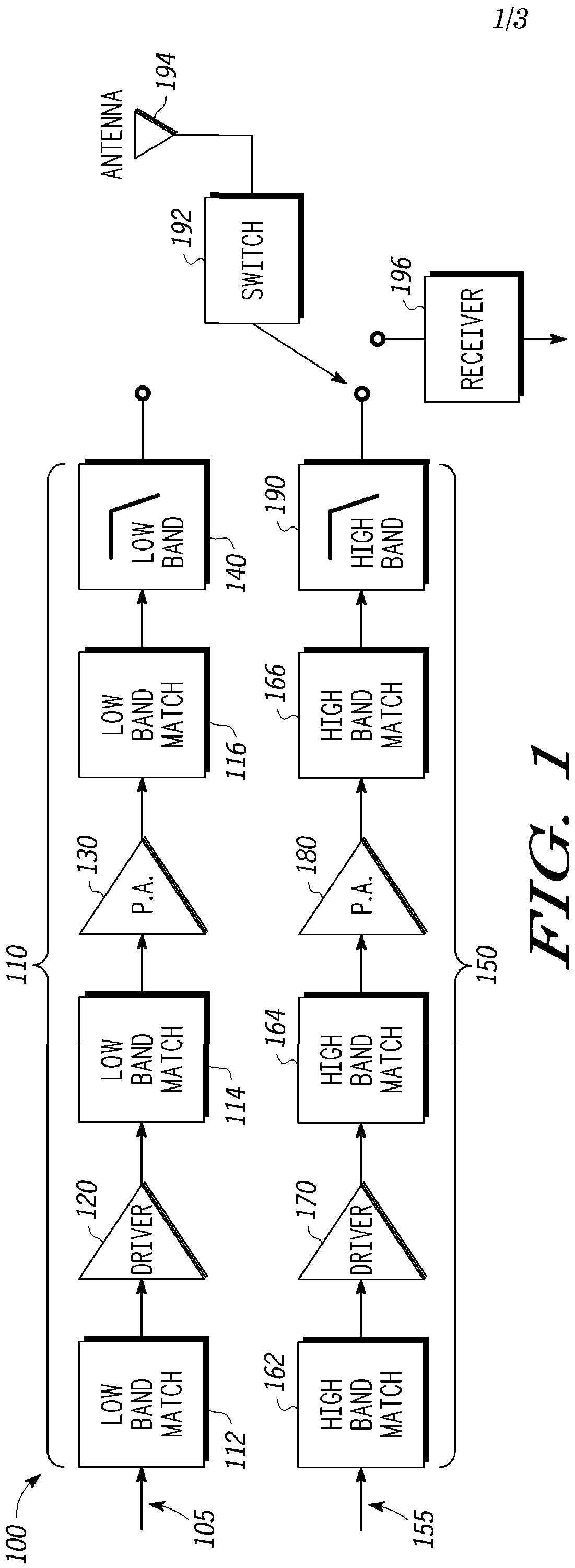
- FIG. 1 is a diagram of a prior art transceiver having a dual power amplifier (PA) line-up;
- PA power amplifier
- FIG. 2 is a diagram of one embodiment of a transceiver including a single PA line-up
- FIG. 3 is a schematic of an embodiment a variable matching circuit included in the single PA line-up of FIG. 2;
- FIG. 4 is a schematic of one embodiment of a variable filter included in the single PA line-up of FIG. 2;
- FIG. 5 is a flow diagram of one embodiment of a method of transmitting a plurality of signals utilizing a single PA line-up.
- a prior art transceiver 100 includes a transmitter having a low frequency power amplifier (PA) line-up 110 for transmitting low frequency signals (e.g., signals having a frequency of 824 MHz to 915 MHz) and a high frequency PA line-up 150 for transmitting high frequency signals (e.g., signals having a frequency of 1710 MHz to 1910 MHz).
- PA power amplifier
- Low frequency PA line-up 110 includes multiple low band matching circuits (e.g., low band matching circuit 112, low band matching circuit 114, and low band matching circuit 116) coupled between various system components (e.g., a driver 120, a PA 130, and a low band filter 140, each of which is discussed below).
- low band matching circuit 112 is coupled to a signal generator (not shown) and an input of driver 120, and is configured to receive low frequency signals 105 from the signal generator.
- Low band matching circuit 114 is coupled to an output of driver 120 and coupled to an input of PA 130
- low band matching circuit 116 is coupled to an output of PA 130 and coupled to an input of low band filter 140.
- high frequency PA line-up 150 also includes multiple high band matching circuits (e.g., high band matching circuit 162, high band matching circuit 164, and high band matching circuit 166) coupled between various system components (e.g., a driver 170, a PA 180, and a high band filter 190, each of which is discussed below).
- high band matching circuit 162 is coupled to the signal generator and an input of driver 170, and is configured to receive high frequency signals 155 from the signal generator.
- High band matching circuit 164 is coupled to an output of driver 170 and coupled to an input of PA 180
- high band matching circuit 166 is coupled to an output of PA 180 and coupled to an input of high band filter 190.
- transceiver 100 includes a switch 192 coupled to an antenna 194, wherein antenna 194 typically includes an impedance requirement for transmitting signals. Furthermore, switch 192 is configured to switch between low frequency PA line-up 110, high frequency PA line-up 150, and a receiver 196.
- transceiver 100 In operation, when transceiver 100 receives a signal (not shown) from, for example, a telecommunications base station (not shown), the signal carrier instructs transceiver 100 which bandwidth (i.e., 824 MHz to 915 MHz or 1710 MHz to 1910 MHz) to utilize when transmitting an output signal. Once transceiver 100 receives this instruction, transceiver 100 will utilize switch 192 to appropriately choose either low frequency PA line-up 110 or high frequency PA line-up 150 depending on whether a low frequency signal 105 or a high frequency signal 155 is to be utilized. [0018] FIG.
- Low/high frequency PA line-up 210 includes a plurality of matching circuits (e.g., matching circuit 212, matching circuit 214, and matching circuit 216) coupled to various system components (e.g., driver 220, PA 230, and low/high band filter 240, each of which is discussed below).
- matching circuits e.g., matching circuit 212, matching circuit 214, and matching circuit 216
- driver 220, PA 230, and low/high band filter 240 e.g., driver 220, PA 230, and low/high band filter 240, each of which is discussed below.
- matching circuit 212 is coupled to an input of a driver 220
- matching circuit 214 is coupled to an output of driver 220 and coupled to an input of a PA 230
- matching circuit 216 is coupled to an output of PA 230 and coupled to an input of a low/high band filter 240
- driver 220 and PA 230 may be any driver or PA, respectively, known in the art or developed in the future capable of amplifying communication signals having low or high frequencies.
- driver 220 and PA 230 are each suitably configured to amplify signals 205 to any desired level.
- driver 220 and PA 230 are each suitably configured to operate at a large enough bandwidth to include substantially all of the frequencies in each of the plurality of bandwidths transmitted by transceiver 200.
- Matching circuits 212, 214, and 216 are each variably configurable to match the impedance of signals 205 between the input and output of their respective system components in transceiver 200.
- matching circuits 212, 214, and 216 are each configurable to variably match the impedance of the system components with which they are respectively coupled between such that low/high frequency PA line-up 210 is capable of transmitting signals having frequencies in more than one frequency band.
- the signals 205 transmitted by low/high frequency PA line-up 210 in one embodiment; include frequencies in a low frequency band (e.g., 824 MHz to 915 MHz) and signals in a high frequency band (e.g., 1710 MHz to 1910 MHz).
- low/high frequency PA line-up 210 is configurable such that low/high frequency PA line-up 210 is able to match the impedance between system components for signals having frequencies in N number of frequency bands, where N is an integer greater than zero.
- matching circuits 212, 214, and 216 are variably configurable to enable proper impedance matching for low/high frequency PA line-up 210 such that signals 205 having a plurality of modulation types may be transmitted.
- low/high frequency PA line-up 210 may be configurable for operating with GSM, Enhanced Data rates for GSM Evolution (EDGE), or Code Division Multiple Access (CDMA) modulations.
- GSM Global System for Mobile Communications
- EDGE Enhanced Data rates for GSM Evolution
- CDMA Code Division Multiple Access
- matching circuits 212, 214, and 216 are variably configurable to enable proper impedance matching for low/high PA line-up 210 for transmitting signals 205 having a plurality of RF power levels.
- low/high frequency PA line-up 210 may be configurable to transmit signals 205 having power in the range of about 1 milliwatts to about 3 Watts.
- matching circuits 212 and 214 are described above as being variably configurable, one embodiment contemplates that only matching circuit 216 is a variable matching circuit and neither matching circuit 212 nor matching circuit 214 are variable matching circuits. In another embodiment, matching circuit 216 and matching circuit 214 are variable matching circuits, and matching circuit 212 is not a variable matching circuit. In yet another embodiment, matching circuit 216 and matching circuit 212 are variable matching circuits, and matching circuit 214 is not a variable matching circuit. Accordingly, when matching circuit 212 and/or 214 are not variable matching circuits, these circuits do not include variable capacitive elements.
- Low/high band filter 240 is configurable to allow desired frequencies to pass through it.
- low/high band filter 240 is a configurable bandpass filter capable of allowing signals 205 in a plurality of frequency bands and modulation types to pass through it.
- Low/high band filter 240 in one embodiment, is configurable to allow signals 205 having frequencies in a low frequency band or signals 205 having frequencies in a high frequency band to pass through low/high band filter 240, depending upon which frequency with which transceiver 200 is transmitting signals.
- low/high band filter 240 is configurable to allow signals 205 having a frequency of, for example, 824 MHz to 915 MHz and 1710 MHz to 1910 MHz to pass through it.
- signals 205 are low frequency signals
- low/high band filter 240 will filter out the harmonic signals of the fundamental frequencies of 824 MHz to 915 MHz.
- signals 205 are high frequency signals
- low/high band filter 240 will filter out the harmonic signals of the fundamental frequencies of 1710 MHz to 1910 MHz.
- low/high PA line-up 210 is capable of tune- matching (via variable matching circuits 212, 214, and 216) a plurality of system components and tune-filtering (via low/high band filter 240) signals 205 having frequencies in multiple frequency bands, multiple modulation types, and/or multiple levels of power.
- low/high band filter 240 is configurable to allow a plurality of signal modulation types to pass through.
- Low/high band filter 240 in one embodiment, is configurable to allow signals having GSM, EDGE, or CDMA modulations to pass through.
- Transceiver 200 also includes a switch 292 to switch between low/high PA lineup 210 and a receiver 296, wherein switch 292 may be any switch known in the art or developed in the future and receiver 296 may be any receiver known in the art or developed in the future.
- receiver 296 is illustrated as having only one receiving path, receiver 296 may include any number of receiving paths to receive signals having frequencies in a plurality of frequency bands.
- switch 292 is coupled to an antenna 294, wherein antenna 294 may be any antenna known in the art or developed in the future.
- antenna 294 includes an impedance requirement of about 50 ⁇ .
- antenna 294 may require any amount of impedance.
- the various system components of low/high frequency PA line-up 210 are each individually and/or collectively configurable to match the overall impedance of PA line-up 210 to the impedance required by antenna 294.
- each of variable matching circuits 212, 214, and 216 are configurable to match the impedance of signals 205 to the inputs and outputs of the system components with which they are respectively coupled between for both low frequency signals and high frequency signals.
- low/high frequency PA line-up 210 is capable of transmitting signals 205 having different frequencies and/or modulations and/or RF power levels. Accordingly, low/high frequency PA line-up 210 is capable of transmitting signals 205 having a frequency in the same frequency band (e.g., 824 MHz to 915 MHz or 1710 MHZ to 1910 MHz), but having different modulation types (e.g., GSM vs. EDGE, GSM vs. CDMA, or EDGE vs. CDMA) and different RF power (e.g., 1 Watt vs. 3 Watts, 0.5 Watts vs.
- modulation types e.g., GSM vs. EDGE, GSM vs. CDMA, or EDGE vs. CDMA
- different RF power e.g., 1 Watt vs. 3 Watts, 0.5 Watts vs.
- signals 205 having the same signal modulation type e.g., CDMA
- signals 205 having the same RF power, but having frequencies in different frequency bands and having different modulation types signals 205 having frequencies in the same frequency band and having the same modulation type, but having different RF power
- signals 205 having frequencies in the same frequency band and having the same RF power, but having different modulation types signals 205 having the same modulation type and the same RF power, but having frequencies in different frequency bands
- low/high frequency PA line-up 210 is capable of transmitting signals 205 having any combination of frequencies in a plurality of frequency bands, modulation types, and RF power levels.
- low/high PA line-up 210 is described as being within transceiver 200, low/high PA line-up 210 may also form a portion of a transmitter. Accordingly, the present disclosure is not limited to transceivers, but also includes any device capable of transmitting signals.
- variable matching circuit 216 includes a variable capacitive element 2160, a variable capacitive element 2161, a capacitive element 2162, a capacitive element 2163, an inductive element 2164, and an inductive element 2165.
- Variable capacitive elements 2160 and 2161 may each be any device capable of variably storing charge for a given electric potential.
- capacitive elements 2160 and 2161 may each be any variable capacitor or variable capacitive element known in the art or developed in the future.
- variable capacitive elements 2160 and 2161 are each micro-electro-mechanical systems (MEMS) capacitive elements.
- MEMS micro-electro-mechanical systems
- capacitive elements 2160 and 2161 are variable capacitive elements. In yet another embodiment, variable capacitive elements 2160 and 2161 are each MEMS variable capacitive elements with separate direct current and radio frequency terminals. In still another embodiment, variable capacitive elements 2160 and 2161 are each tunable MEMS variable capacitive elements with separate direct current and radio frequency terminals. In still another embodiment, variable capacitive elements 2160 and 2161 are each binary MEMS variable capacitive elements with separate DC and RF terminals.
- capacitive elements 2160 and 2161 are each capacitive elements in the range of about 0.5 picofarads (pF) to about 30 pF and capable of being switched ON/OFF. Including separate DC terminals in capacitive elements 2160 and 2161, in various embodiments, enables variable matching circuit 216 to realize proper re-configuration without introducing coupling between DC and RF signals.
- capacitive elements 2162 and 2163 are each capacitive elements in the range of about 0.5 pF to about 30 pF. Accordingly, capacitive elements 2162 and 2163 may be any capacitive element know in the art or developed in the future.
- inductive elements 2164 and 2165 are each inductive elements in the range of about 0.2 nanohenries (nH) to about 10 nH. As such, inductive elements 2164 and 2165 may be any inductive element known in the art or developed in the future.
- variable capacitive element 2160 is coupled in parallel with capacitive element 2162, and variable capacitive element 2160 and capacitive element 2162 are coupled to inductive element 2164 via a node 2166.
- inductive element 2165 is coupled to node 2166 and coupled to variable capacitive element 2161 and capacitive element 2163 via a node 2167, wherein variable capacitive element 2161 and capacitive element 2163 are coupled in parallel with each other.
- variable matching circuit 216 is illustrated with two variable capacitive elements, two capacitive elements, and two inductive elements, however, various embodiments contemplate the use of any number of variable capacitive elements, capacitive elements, and inductive elements to realize the re-configuration of PA 230 output matching for operation in different frequency bands.
- variable matching circuit 216 is capable of impedance matching for at least two frequency bands, and/or for at least two signal modulation types, and/or for at least two power levels.
- variable matching circuits 212 and 214 are configured to operate in a manner similar to variable matching circuit 216 to match the system components with which they are respectively coupled between.
- FIG. 4 is a schematic of one embodiment of low/high band filter 240.
- low/high band filter 240 is a variable harmonic filter including four variable capacitive elements 2400-2403, four capacitive elements 2404- 2407, and two inductive elements 2408-2409.
- Variable capacitive elements 2400-2403 may each be any device capable of variably storing charge for a given electric potential.
- capacitive elements 2400-2403 may each be any variable capacitor or variable capacitive element known in the art or developed in the future.
- variable capacitive elements 2400-2403 are each MEMS variable capacitive elements.
- variable capacitive elements 2400-2403 are each MEMS variable capacitive elements with separate direct current and radio frequency terminals.
- variable capacitive elements 2400-2403 are each tunable MEMS variable capacitive elements with separate direct current and radio frequency terminals.
- variable capacitive elements 2400-2403 are each binary MEMS variable capacitive elements with separate DC and RF terminals.
- capacitive elements 2400-2403 are each capacitive elements in the range of about 0.5 pF to about 30 pF and capable of being switched ON/OFF. Including separate DC terminals in capacitive elements 2400-2403 in various embodiments enables low/high band filter 240 to properly switch state without introducing coupling between DC and RF signals.
- Capacitive elements 2404-2407 may be any capacitor or capacitive element know in the art or developed in the future. In accordance with one embodiment, capacitive elements 2404-2407 are each capacitive elements in the range of about 0.2 pF to about 10 pF.
- inductive elements 2408 and 2409 may be any inductor or inductive element known in the art or developed in the future. In accordance with one embodiment, inductive elements 2408 and 2409 are each inductive elements in the range of about 1.0 nH to about 10 nH.
- variable capacitive element 2400 is coupled in parallel with capacitive element 2404 and inductive element 2408.
- variable capacitive element 2401 is coupled in parallel with capacitive element 2405
- variable capacitive element 2401 and capacitive element 2405 are coupled to variable capacitive element 2400, capacitive element 2404, and inductive element 2408 via a node 2410.
- variable capacitive element 2402 is coupled in parallel with capacitive element 2406 and inductive element 2409, and coupled to variable capacitive element 2401 and capacitive element 2405 via node 2410.
- variable capacitive element 2403 is coupled in parallel with capacitive element 2407, and coupled to variable capacitive element 2402, capacitive element 2406, and inductive element 2409 via a node 2411.
- low/high band filter 240 is illustrated with four variable capacitive elements, four capacitive elements, and two inductive elements, however, various embodiments contemplate the use of any number of variable capacitive elements, capacitive elements, and inductive elements to filter out signals having unwanted frequencies (i.e., signals having frequencies outside the desired transmitted frequency band).
- a controller (not shown) switches OFF variable capacitive elements 2400-2403 to filter out harmonics of the high band fundamental frequency signal. Moreover, the controller switches ON variable capacitive elements 2400-2403 to filter out harmonics of the low band fundamental frequency signal. Accordingly, low/high band filter 240 is capable of allowing signals having frequencies in more than one frequency band to pass through it.
- FIG. 5 is a flow diagram of one embodiment of a method 500 to transmit a plurality of communication signals with different characteristics from a single power amplifier line-up (e.g., low/high frequency PA line-up 210).
- Method 500 initiates by low/high frequency PA line-up 210 transmitting a first signal including the characteristics of a first frequency, a first modulation type, and a first RF power level to an external device (e.g., a telecommunications base-station) (block 510).
- an external device e.g., a telecommunications base-station
- method 500 includes low/high frequency PA line-up 210 transmitting a second signal including the characteristics of a second frequency, a second modulation type, and a second RF power level to the external device, wherein at least one characteristic of the first signal is different from a characteristic of the second signal (block 520).
- method 500 includes low/high frequency PA line-up 210 transmitting the first signal and the second signal with frequencies in the same frequency band (e.g., 824 MHz to 915 MHz, 1710 MHZ to 1910 MHz, and the like), but with different modulation types (e.g., GSM, EDGE, CDMA, or the like) and different RF power levels (e.g., 1 milliWatt to 3 Watts) (block 530).
- method 500 includes low/high frequency PA line-up 210 transmitting the first signal and the second signal with the same signal modulation type (e.g., CDMA), but having frequencies in different frequency bands and with different RF power levels (block 540).
- method 500 includes low/high frequency PA line-up 210 transmitting the first signal and the second signal with the same RF power level, but with frequencies in different frequency bands and with different modulation types (block 550).
- Method 500 includes low/high frequency PA line-up 210 transmitting the first signal and the second signal with frequencies in the same frequency band and with the same modulation type, but having different RF power levels (block 560).
- method 500 includes low/high frequency PA line-up 210 transmitting the first signal and the second signal with frequencies in the same frequency band and with the same RF power level, but having different modulation types (block 570).
- method 500 includes low/high frequency PA line-up 210 transmitting the first signal and the second signal with the same modulation type and the same RF power level, but having frequencies in different frequency bands (block 580). In still another embodiment, method 500 includes low/high frequency PA line-up 210 transmitting the first signal and the second signal with frequencies in different frequency bands, with different modulation types, and with different RF power levels (block 590).
- various embodiments include an apparatus for matching signal impedance between a power amplifier line-up and an antenna.
- the apparatus comprises a variable matching circuit comprising a first input, a first output, and at least a first variable capacitive element, wherein the first input is configured to receive signals from a power amplifier, the variable matching circuit is configured to selectively enable the first variable capacitive element to produce impedance-matched signals; and a variable harmonic filter comprising a second input, a second output, and at least a second variable capacitive element, wherein the second input is coupled to the first output and configured to receive the impedance-matched signals, the variable harmonic filter is configured to selectively enable the second variable capacitive element to filter out undesirable harmonics of the impedance-matched signals to produce filtered, impedance- matched signals, and the second output is configured to be coupled to the antenna.
- variable matching circuit is configured to selectively enable the first variable capacitance element and the variable harmonic filter is configured to selectively enable the second variable capacitive element such that the filtered, impedance-matched signals include at least one of frequencies in a plurality of different frequency bands, a plurality of different modulation types, and a plurality of different RF power levels.
- variable matching circuit is configured to selectively enable the first variable capacitance element and the variable harmonic filter is configured to selectively enable the second variable capacitive element such that the filtered, impedance-matched signals include at least one of frequencies in a plurality of different frequency bands, and wherein a first frequency band is in the range of 824 MHz to 915 MHz, and a second frequency band is in the range of 1710 MHz to 1910 MHz.
- the first variable capacitive element and/or the second variable capacitive element in one embodiment, comprises at least one direct current (DC) terminal and at least one radio frequency (RF) terminal separate from the DC terminal.
- first variable capacitive element and/or the second variable capacitive element is a/are micro-electro-mechanical systems (MEMS) capacitive element(s).
- first variable capacitive element and/or the second variable capacitive element is a/are tunable MEMS capacitive element(s).
- first variable capacitive element and/or the second variable capacitive element is a/are binary MEMS capacitive element(s).
- Various other embodiments include a system for matching signal impedance between a power amplifier line-up and an antenna.
- the system comprises a first matching circuit comprising a first input, a first output, and at least a first capacitive element, wherein the input is configured to be coupled to a signal generator and receive a signal from the signal generator, the first matching circuit is configured to impedance match the signal to produce a first impedance-matched signal; a driver comprising a second input and a second output, wherein the second input is coupled to the first output and configured to receive the first impedance-matched signal, the driver is configured to amplify the first impedance-matched signal to produce a first amplified, impedance-matched signal; a second matching circuit comprising a third input, a third output, and at least a second capacitive element, wherein the third input is coupled to the second output and configured to receive the first amplified, impedance-matched signal, the second matching circuit is configured to impedance match the
- variable matching circuit is configured to selectively enable the first variable capacitance element and the variable harmonic filter is configured to selectively enable the second variable capacitive element such that the filtered, third impedance-matched signal includes at least one of frequencies in a plurality of different frequency bands, a plurality of different modulation types, and a plurality of different RF power levels.
- variable matching circuit is configured to selectively enable the first variable capacitance element and the variable harmonic filter is configured to selectively enable the second variable capacitive element such that the filtered, third impedance-matched signal includes at least one of frequencies in a plurality of different frequency bands, and wherein a first frequency band is in the range of 824 MHz to 915 MHz, and a second frequency band is in the range of 1710 MHz to 1910 MHz.
- the first variable capacitive element and/or the second variable capacitive element in one embodiment, comprises at least one direct current (DC) terminal and at least one radio frequency (RF) terminal separate from the DC terminal.
- the first variable capacitive element and/or the second variable capacitive element is a/are micro-electro-mechanical systems (MEMS) capacitive element(s).
- MEMS micro-electro-mechanical systems
- the first variable capacitive element and/or the second variable capacitive element is a/are tunable MEMS capacitive element(s).
- the first variable capacitive element and/or the second variable capacitive element is a/are binary MEMS capacitive element(s).
- the first matching circuit, the driver, the second matching circuit, the power amplifier, the variable matching circuit, and the variable harmonic filter form a single line-up.
- the first matching circuit is a second variable matching circuit comprising at least a third variable capacitive element.
- the second matching circuit is a third variable matching circuit comprising at least a fourth variable capacitive element.
- various other embodiments include a method to transmit a plurality of communication signals with different characteristics from a single power amplifier lineup to an antenna.
- the method comprises transmitting a first signal including the characteristics of a first frequency, a first modulation type, and a first radio frequency (RF) power level to the external device, and transmitting a second signal including the characteristics of a second frequency, a second modulation type, and a second RF power level to the external device, wherein at least one characteristic of the first signal is different from at least one characteristic of the second signal.
- at least two characteristics of the first signal are different from at least two characteristics of the second signal.
- each of the characteristics of the first signal are different from each of the characteristics of the second signal.
Landscapes
- Engineering & Computer Science (AREA)
- Computer Networks & Wireless Communication (AREA)
- Signal Processing (AREA)
- Transmitters (AREA)
- Amplifiers (AREA)
- Transceivers (AREA)
Abstract
Description
Claims




Priority Applications (2)
| Application Number | Priority Date | Filing Date | Title |
|---|---|---|---|
| JP2009521866A JP5448163B2 (en) | 2006-07-28 | 2007-04-24 | Reconfigurable impedance matching and harmonic filter system |
| CN200780027714.XA CN101502004B (en) | 2006-07-28 | 2007-04-24 | Re-configurable impedance matching and harmonic filter system |
Applications Claiming Priority (2)
| Application Number | Priority Date | Filing Date | Title |
|---|---|---|---|
| US11/494,821 US7567782B2 (en) | 2006-07-28 | 2006-07-28 | Re-configurable impedance matching and harmonic filter system |
| US11/494,821 | 2006-07-28 |
Publications (3)
| Publication Number | Publication Date |
|---|---|
| WO2008014029A2 true WO2008014029A2 (en) | 2008-01-31 |
| WO2008014029A3 WO2008014029A3 (en) | 2008-11-27 |
| WO2008014029A8 WO2008014029A8 (en) | 2009-03-26 |
Family
ID=38982155
Family Applications (1)
| Application Number | Title | Priority Date | Filing Date |
|---|---|---|---|
| PCT/US2007/067257 Ceased WO2008014029A2 (en) | 2006-07-28 | 2007-04-24 | Re-configurable impedance matching and harmonic filter system |
Country Status (5)
| Country | Link |
|---|---|
| US (1) | US7567782B2 (en) |
| JP (1) | JP5448163B2 (en) |
| CN (1) | CN101502004B (en) |
| TW (1) | TW200824308A (en) |
| WO (1) | WO2008014029A2 (en) |
Cited By (7)
| Publication number | Priority date | Publication date | Assignee | Title |
|---|---|---|---|---|
| WO2012061244A1 (en) * | 2010-11-01 | 2012-05-10 | Cree, Inc. | Matching network for transmission circuitry |
| JP2013502189A (en) * | 2009-08-14 | 2013-01-17 | クゥアルコム・インコーポレイテッド | Amplifier with variable matching circuit to improve linearity |
| JP2013502846A (en) * | 2009-08-19 | 2013-01-24 | クゥアルコム・インコーポレイテッド | Digital tunable interstage matching circuit |
| US8750810B2 (en) | 2009-07-24 | 2014-06-10 | Qualcomm Incorporated | Power amplifier with switched output matching for multi-mode operation |
| US8963611B2 (en) | 2009-06-19 | 2015-02-24 | Qualcomm Incorporated | Power and impedance measurement circuits for a wireless communication device |
| US9143172B2 (en) | 2009-06-03 | 2015-09-22 | Qualcomm Incorporated | Tunable matching circuits for power amplifiers |
| US9559639B2 (en) | 2009-08-19 | 2017-01-31 | Qualcomm Incorporated | Protection circuit for power amplifier |
Families Citing this family (49)
| Publication number | Priority date | Publication date | Assignee | Title |
|---|---|---|---|---|
| US8744384B2 (en) | 2000-07-20 | 2014-06-03 | Blackberry Limited | Tunable microwave devices with auto-adjusting matching circuit |
| US7711337B2 (en) | 2006-01-14 | 2010-05-04 | Paratek Microwave, Inc. | Adaptive impedance matching module (AIMM) control architectures |
| US7714676B2 (en) | 2006-11-08 | 2010-05-11 | Paratek Microwave, Inc. | Adaptive impedance matching apparatus, system and method |
| US7535312B2 (en) | 2006-11-08 | 2009-05-19 | Paratek Microwave, Inc. | Adaptive impedance matching apparatus, system and method with improved dynamic range |
| US8364102B2 (en) * | 2007-04-19 | 2013-01-29 | Intel Corporation | Universal front end module for networking device |
| US7917104B2 (en) | 2007-04-23 | 2011-03-29 | Paratek Microwave, Inc. | Techniques for improved adaptive impedance matching |
| US7991363B2 (en) | 2007-11-14 | 2011-08-02 | Paratek Microwave, Inc. | Tuning matching circuits for transmitter and receiver bands as a function of transmitter metrics |
| US8131244B2 (en) * | 2007-12-12 | 2012-03-06 | Broadcom Corporation | Method and system for dynamically adjusting intermediate frequency (IF) and filtering for microwave circuits |
| US8072285B2 (en) | 2008-09-24 | 2011-12-06 | Paratek Microwave, Inc. | Methods for tuning an adaptive impedance matching network with a look-up table |
| US8055212B2 (en) * | 2009-05-26 | 2011-11-08 | ST-Erisson SA | Transmitter phase shift determination and compensation |
| US9026062B2 (en) | 2009-10-10 | 2015-05-05 | Blackberry Limited | Method and apparatus for managing operations of a communication device |
| TWI407690B (en) * | 2010-01-19 | 2013-09-01 | Htc Corp | Broadband antenna matching apparatus and method thereof |
| US8803631B2 (en) | 2010-03-22 | 2014-08-12 | Blackberry Limited | Method and apparatus for adapting a variable impedance network |
| CN101814927B (en) * | 2010-04-14 | 2014-07-02 | 中兴通讯股份有限公司 | Multimode all-frequency-band radio-frequency emitting device and method |
| WO2011133657A2 (en) | 2010-04-20 | 2011-10-27 | Paratek Microwave, Inc. | Method and apparatus for managing interference in a communication device |
| CN101902243B (en) * | 2010-07-28 | 2013-01-02 | 锐迪科创微电子(北京)有限公司 | Configurable multimode radio-frequency front end module and mobile terminal having same |
| CN102135614B (en) * | 2011-01-10 | 2012-11-07 | 同致电子科技(昆山)有限公司 | Circuit for automatically adjusting aftershock of reverse radar sensor |
| JP5648697B2 (en) | 2011-01-19 | 2015-01-07 | 株式会社村田製作所 | Variable reactance circuit and antenna device |
| US8712340B2 (en) | 2011-02-18 | 2014-04-29 | Blackberry Limited | Method and apparatus for radio antenna frequency tuning |
| US8594584B2 (en) | 2011-05-16 | 2013-11-26 | Blackberry Limited | Method and apparatus for tuning a communication device |
| US9564676B2 (en) * | 2011-06-30 | 2017-02-07 | Google Technology Holdings LLC | System and methods for adaptive antenna optimization |
| US9769826B2 (en) | 2011-08-05 | 2017-09-19 | Blackberry Limited | Method and apparatus for band tuning in a communication device |
| CN103138713A (en) * | 2011-11-22 | 2013-06-05 | 中国科学院电子学研究所 | Reconfigurable complex filter and implementation method |
| US20130156074A1 (en) * | 2011-12-14 | 2013-06-20 | Aviacomm Inc. | Wideband rf front-end |
| KR20130093996A (en) * | 2012-02-15 | 2013-08-23 | 한국전자통신연구원 | Impedance matching circuit, power amplifier and manufacturing method for variable capacitor |
| GB2491238B (en) * | 2012-05-15 | 2013-07-03 | Renesas Mobile Corp | Filter circuitry |
| US9853363B2 (en) | 2012-07-06 | 2017-12-26 | Blackberry Limited | Methods and apparatus to control mutual coupling between antennas |
| US9350405B2 (en) | 2012-07-19 | 2016-05-24 | Blackberry Limited | Method and apparatus for antenna tuning and power consumption management in a communication device |
| WO2014013869A1 (en) * | 2012-07-20 | 2014-01-23 | 株式会社村田製作所 | Amplifying module and transmitting module provided with same |
| US9374113B2 (en) * | 2012-12-21 | 2016-06-21 | Blackberry Limited | Method and apparatus for adjusting the timing of radio antenna tuning |
| US10404295B2 (en) | 2012-12-21 | 2019-09-03 | Blackberry Limited | Method and apparatus for adjusting the timing of radio antenna tuning |
| WO2015093462A1 (en) | 2013-12-20 | 2015-06-25 | 株式会社村田製作所 | High-frequency circuit and transceiver circuit using high-frequency circuit |
| US20170019137A1 (en) * | 2014-04-07 | 2017-01-19 | Cavendish Kinetics, Inc. | Device with variable frequency filter for rejecting harmonics |
| US9537452B2 (en) * | 2014-04-29 | 2017-01-03 | Skyworks Solutions, Inc. | Broadband power amplifier systems and methods |
| US20160191085A1 (en) * | 2014-08-13 | 2016-06-30 | Skyworks Solutions, Inc. | Transmit front end module for dual antenna applications |
| DE102014113910A1 (en) * | 2014-09-25 | 2016-03-31 | Huf Hülsbeck & Fürst Gmbh & Co. Kg | Antenna circuit for near-field antennas |
| US9438319B2 (en) | 2014-12-16 | 2016-09-06 | Blackberry Limited | Method and apparatus for antenna selection |
| US11211954B2 (en) * | 2015-03-10 | 2021-12-28 | Blackberry Limited | Supporting multiple frequency bands |
| US9882538B2 (en) * | 2015-03-24 | 2018-01-30 | Skyworks Solutions, Inc. | Distributed output matching network for a radio frequency power amplifier module |
| WO2017062650A1 (en) * | 2015-10-06 | 2017-04-13 | Resonant Inc. | Radio frequency transmit filter with integrated impedance matching network |
| US10523261B2 (en) * | 2016-03-31 | 2019-12-31 | Apple Inc. | Co-channel wireless detection |
| CN106130493A (en) * | 2016-08-29 | 2016-11-16 | 贵州航天林泉电机有限公司 | A kind of low cost microwave radio controlled power amplifying circuit |
| US10404740B2 (en) * | 2016-10-03 | 2019-09-03 | Telepathy Labs, Inc. | System and method for deprovisioning |
| US10305532B1 (en) * | 2018-03-16 | 2019-05-28 | Blackberry Limited | Systems and methods to dynamically change reactance to support multiple RF frequencies |
| CN112400281B (en) * | 2018-06-26 | 2022-02-01 | 株式会社村田制作所 | High-frequency module and communication device |
| CN115001539A (en) * | 2019-04-11 | 2022-09-02 | 奈克赛特公司 | Wireless device configured to transmit power using harvested energy |
| US10658999B1 (en) * | 2019-07-09 | 2020-05-19 | Silicon Laboratories Inc. | On-chip harmonic filtering for radio frequency (RF) communications |
| US11817832B2 (en) | 2020-01-03 | 2023-11-14 | Skyworks Solutions, Inc. | Power amplifier output matching |
| CN112087240B (en) * | 2020-08-13 | 2021-10-08 | 深圳市万联航通电子科技有限公司 | Reconfigurable radio frequency front end and universal device of unmanned aerial vehicle data link |
Family Cites Families (17)
| Publication number | Priority date | Publication date | Assignee | Title |
|---|---|---|---|---|
| JPS6028315A (en) * | 1983-07-27 | 1985-02-13 | Hitachi Ltd | Input filter |
| US5371481A (en) * | 1993-03-24 | 1994-12-06 | Nokia Mobile Phones Ltd. | Tuning techniques for I/Q channel signals in microwave digital transmission systems |
| JP2713128B2 (en) * | 1993-12-28 | 1998-02-16 | 日本電気株式会社 | Diversity reception signal synthesis circuit |
| US6078794A (en) * | 1997-02-19 | 2000-06-20 | Motorola, Inc. | Impedance matching for a dual band power amplifier |
| MY128729A (en) * | 1997-02-25 | 2007-02-28 | Ericsson Telefon Ab L M | Device and process for telecommunication |
| US6307452B1 (en) * | 1999-09-16 | 2001-10-23 | Motorola, Inc. | Folded spring based micro electromechanical (MEM) RF switch |
| JP2001185962A (en) * | 1999-12-27 | 2001-07-06 | Toshiba Corp | Amplifier |
| US6307169B1 (en) * | 2000-02-01 | 2001-10-23 | Motorola Inc. | Micro-electromechanical switch |
| US6384353B1 (en) * | 2000-02-01 | 2002-05-07 | Motorola, Inc. | Micro-electromechanical system device |
| US6507475B1 (en) * | 2000-06-27 | 2003-01-14 | Motorola, Inc. | Capacitive device and method of manufacture |
| JP2003124754A (en) * | 2001-10-18 | 2003-04-25 | Hitachi Ltd | High frequency amplifier |
| US6706548B2 (en) * | 2002-01-08 | 2004-03-16 | Motorola, Inc. | Method of making a micromechanical device |
| US6794101B2 (en) * | 2002-05-31 | 2004-09-21 | Motorola, Inc. | Micro-electro-mechanical device and method of making |
| ATE353774T1 (en) * | 2002-06-25 | 2007-03-15 | Asahi Kasei Chemicals Corp | PHOTOSENSITIVE RESIN COMPOSITION FOR PRINTING PLATE WHICH CAN BE ENGRAVED BY LASER |
| JP2004254155A (en) * | 2003-02-21 | 2004-09-09 | Kanji Otsuka | Signal transmission device and wiring structure |
| US7561851B2 (en) * | 2004-04-01 | 2009-07-14 | Harris Stratex Networks, Inc. | System and method for calibrating modules of a wide-range transceiver |
| JP2006005848A (en) * | 2004-06-21 | 2006-01-05 | Sharp Corp | Power amplifier and high-frequency communication device |
-
2006
- 2006-07-28 US US11/494,821 patent/US7567782B2/en active Active
-
2007
- 2007-04-24 CN CN200780027714.XA patent/CN101502004B/en not_active Expired - Fee Related
- 2007-04-24 WO PCT/US2007/067257 patent/WO2008014029A2/en not_active Ceased
- 2007-04-24 JP JP2009521866A patent/JP5448163B2/en not_active Expired - Fee Related
- 2007-05-10 TW TW096116658A patent/TW200824308A/en unknown
Cited By (13)
| Publication number | Priority date | Publication date | Assignee | Title |
|---|---|---|---|---|
| US9143172B2 (en) | 2009-06-03 | 2015-09-22 | Qualcomm Incorporated | Tunable matching circuits for power amplifiers |
| US8963611B2 (en) | 2009-06-19 | 2015-02-24 | Qualcomm Incorporated | Power and impedance measurement circuits for a wireless communication device |
| US8750810B2 (en) | 2009-07-24 | 2014-06-10 | Qualcomm Incorporated | Power amplifier with switched output matching for multi-mode operation |
| JP2013502189A (en) * | 2009-08-14 | 2013-01-17 | クゥアルコム・インコーポレイテッド | Amplifier with variable matching circuit to improve linearity |
| US8779857B2 (en) | 2009-08-14 | 2014-07-15 | Qualcomm Incorporated | Amplifier with variable matching circuit to improve linearity |
| JP2013502846A (en) * | 2009-08-19 | 2013-01-24 | クゥアルコム・インコーポレイテッド | Digital tunable interstage matching circuit |
| US9559639B2 (en) | 2009-08-19 | 2017-01-31 | Qualcomm Incorporated | Protection circuit for power amplifier |
| JP2016189592A (en) * | 2009-08-19 | 2016-11-04 | クゥアルコム・インコーポレイテッドQualcomm Incorporated | Digital tunable inter-stage matching circuit |
| JP2014239472A (en) * | 2009-08-19 | 2014-12-18 | クゥアルコム・インコーポレイテッドQualcomm Incorporated | Digital tunable inter-stage matching circuit |
| US9000847B2 (en) | 2009-08-19 | 2015-04-07 | Qualcomm Incorporated | Digital tunable inter-stage matching circuit |
| US8611834B2 (en) | 2010-11-01 | 2013-12-17 | Cree, Inc. | Matching network for transmission circuitry |
| US8855584B2 (en) | 2010-11-01 | 2014-10-07 | Cree, Inc. | Matching network for transmission circuitry |
| WO2012061244A1 (en) * | 2010-11-01 | 2012-05-10 | Cree, Inc. | Matching network for transmission circuitry |
Also Published As
| Publication number | Publication date |
|---|---|
| WO2008014029A8 (en) | 2009-03-26 |
| WO2008014029A3 (en) | 2008-11-27 |
| US7567782B2 (en) | 2009-07-28 |
| TW200824308A (en) | 2008-06-01 |
| JP2009545240A (en) | 2009-12-17 |
| US20080026709A1 (en) | 2008-01-31 |
| JP5448163B2 (en) | 2014-03-19 |
| CN101502004A (en) | 2009-08-05 |
| CN101502004B (en) | 2013-03-13 |
Similar Documents
| Publication | Publication Date | Title |
|---|---|---|
| US7567782B2 (en) | Re-configurable impedance matching and harmonic filter system | |
| US11689164B2 (en) | Multi-band power amplifier module | |
| US20120163245A1 (en) | Module for mobile communication terminal and mobile communication terminal | |
| US10277287B2 (en) | Antenna system and harmonic suppression element | |
| CN108288958B (en) | Low-pass filter | |
| WO2008063740A2 (en) | Transmitter with improved power efficiency | |
| CN105375883B (en) | Doherty power amplifier combiner with adjustable impedance termination circuit | |
| US11451198B2 (en) | Multi-band power amplifier module | |
| EP1305885B1 (en) | Method and apparatus for multiple band transmission | |
| CN109417397A (en) | Integrated signal combiner | |
| US10374784B2 (en) | Adaptive multi-carrier filter response systems and methods | |
| KR20160058844A (en) | Systems and methods related to carrier aggregation front-end module applications | |
| KR20080104380A (en) | Transmitters, Power Amplifiers, Filtering Methods, and Transceivers | |
| KR20140085335A (en) | Semiconductor device and adjustment method of filter circuit | |
| US10505702B2 (en) | Transmission/reception module | |
| CN111819791B (en) | Multiplexer, high frequency front end circuit and communication device | |
| CN112400281A (en) | High-frequency module and communication device | |
| US20140254568A1 (en) | Semiconductor module | |
| CN115250095A (en) | Power amplifying module | |
| CN110661543B (en) | Mobile phone device, radio frequency transceiver circuit and impedance adjusting device | |
| US20220311455A1 (en) | Radio-frequency circuit and communication device | |
| CN105490698A (en) | Aggregate signal amplification device and method |
Legal Events
| Date | Code | Title | Description |
|---|---|---|---|
| WWE | Wipo information: entry into national phase |
Ref document number: 200780027714.X Country of ref document: CN |
|
| 121 | Ep: the epo has been informed by wipo that ep was designated in this application |
Ref document number: 07761157 Country of ref document: EP Kind code of ref document: A2 |
|
| WWE | Wipo information: entry into national phase |
Ref document number: 2009521866 Country of ref document: JP |
|
| NENP | Non-entry into the national phase |
Ref country code: DE |
|
| NENP | Non-entry into the national phase |
Ref country code: RU |
|
| 122 | Ep: pct application non-entry in european phase |
Ref document number: 07761157 Country of ref document: EP Kind code of ref document: A2 |