WO2007129702A1 - ケイ素含有化合物及びそれを利用した有機エレクトロルミネッセンス素子 - Google Patents

ケイ素含有化合物及びそれを利用した有機エレクトロルミネッセンス素子 Download PDF

Info

Publication number
WO2007129702A1
WO2007129702A1 PCT/JP2007/059499 JP2007059499W WO2007129702A1 WO 2007129702 A1 WO2007129702 A1 WO 2007129702A1 JP 2007059499 W JP2007059499 W JP 2007059499W WO 2007129702 A1 WO2007129702 A1 WO 2007129702A1
Authority
WO
WIPO (PCT)
Prior art keywords
group
substituted
carbon atoms
unsubstituted
general formula
Prior art date
Legal status (The legal status is an assumption and is not a legal conclusion. Google has not performed a legal analysis and makes no representation as to the accuracy of the status listed.)
Ceased
Application number
PCT/JP2007/059499
Other languages
English (en)
French (fr)
Inventor
Mitsunori Ito
Current Assignee (The listed assignees may be inaccurate. Google has not performed a legal analysis and makes no representation or warranty as to the accuracy of the list.)
Idemitsu Kosan Co Ltd
Original Assignee
Idemitsu Kosan Co Ltd
Priority date (The priority date is an assumption and is not a legal conclusion. Google has not performed a legal analysis and makes no representation as to the accuracy of the date listed.)
Filing date
Publication date
Application filed by Idemitsu Kosan Co Ltd filed Critical Idemitsu Kosan Co Ltd
Priority to JP2008514495A priority Critical patent/JPWO2007129702A1/ja
Priority to US12/299,967 priority patent/US20090236975A1/en
Publication of WO2007129702A1 publication Critical patent/WO2007129702A1/ja
Anticipated expiration legal-status Critical
Ceased legal-status Critical Current

Links

Classifications

    • CCHEMISTRY; METALLURGY
    • C07ORGANIC CHEMISTRY
    • C07FACYCLIC, CARBOCYCLIC OR HETEROCYCLIC COMPOUNDS CONTAINING ELEMENTS OTHER THAN CARBON, HYDROGEN, HALOGEN, OXYGEN, NITROGEN, SULFUR, SELENIUM OR TELLURIUM
    • C07F7/00Compounds containing elements of Groups 4 or 14 of the Periodic Table
    • C07F7/02Silicon compounds
    • C07F7/08Compounds having one or more C—Si linkages
    • C07F7/0803Compounds with Si-C or Si-Si linkages
    • C07F7/0805Compounds with Si-C or Si-Si linkages comprising only Si, C or H atoms
    • CCHEMISTRY; METALLURGY
    • C07ORGANIC CHEMISTRY
    • C07FACYCLIC, CARBOCYCLIC OR HETEROCYCLIC COMPOUNDS CONTAINING ELEMENTS OTHER THAN CARBON, HYDROGEN, HALOGEN, OXYGEN, NITROGEN, SULFUR, SELENIUM OR TELLURIUM
    • C07F7/00Compounds containing elements of Groups 4 or 14 of the Periodic Table
    • C07F7/02Silicon compounds
    • C07F7/08Compounds having one or more C—Si linkages
    • C07F7/0803Compounds with Si-C or Si-Si linkages
    • C07F7/081Compounds with Si-C or Si-Si linkages comprising at least one atom selected from the elements N, O, halogen, S, Se or Te
    • C07F7/0812Compounds with Si-C or Si-Si linkages comprising at least one atom selected from the elements N, O, halogen, S, Se or Te comprising a heterocyclic ring
    • HELECTRICITY
    • H10SEMICONDUCTOR DEVICES; ELECTRIC SOLID-STATE DEVICES NOT OTHERWISE PROVIDED FOR
    • H10KORGANIC ELECTRIC SOLID-STATE DEVICES
    • H10K50/00Organic light-emitting devices
    • H10K50/10OLEDs or polymer light-emitting diodes [PLED]
    • H10K50/11OLEDs or polymer light-emitting diodes [PLED] characterised by the electroluminescent [EL] layers
    • HELECTRICITY
    • H10SEMICONDUCTOR DEVICES; ELECTRIC SOLID-STATE DEVICES NOT OTHERWISE PROVIDED FOR
    • H10KORGANIC ELECTRIC SOLID-STATE DEVICES
    • H10K50/00Organic light-emitting devices
    • H10K50/10OLEDs or polymer light-emitting diodes [PLED]
    • H10K50/14Carrier transporting layers
    • HELECTRICITY
    • H10SEMICONDUCTOR DEVICES; ELECTRIC SOLID-STATE DEVICES NOT OTHERWISE PROVIDED FOR
    • H10KORGANIC ELECTRIC SOLID-STATE DEVICES
    • H10K85/00Organic materials used in the body or electrodes of devices covered by this subclass
    • H10K85/10Organic polymers or oligomers
    • H10K85/111Organic polymers or oligomers comprising aromatic, heteroaromatic, or aryl chains, e.g. polyaniline, polyphenylene or polyphenylene vinylene
    • HELECTRICITY
    • H10SEMICONDUCTOR DEVICES; ELECTRIC SOLID-STATE DEVICES NOT OTHERWISE PROVIDED FOR
    • H10KORGANIC ELECTRIC SOLID-STATE DEVICES
    • H10K85/00Organic materials used in the body or electrodes of devices covered by this subclass
    • H10K85/30Coordination compounds
    • H10K85/321Metal complexes comprising a group IIIA element, e.g. Tris (8-hydroxyquinoline) gallium [Gaq3]
    • H10K85/324Metal complexes comprising a group IIIA element, e.g. Tris (8-hydroxyquinoline) gallium [Gaq3] comprising aluminium, e.g. Alq3
    • HELECTRICITY
    • H10SEMICONDUCTOR DEVICES; ELECTRIC SOLID-STATE DEVICES NOT OTHERWISE PROVIDED FOR
    • H10KORGANIC ELECTRIC SOLID-STATE DEVICES
    • H10K85/00Organic materials used in the body or electrodes of devices covered by this subclass
    • H10K85/40Organosilicon compounds, e.g. TIPS pentacene
    • HELECTRICITY
    • H10SEMICONDUCTOR DEVICES; ELECTRIC SOLID-STATE DEVICES NOT OTHERWISE PROVIDED FOR
    • H10KORGANIC ELECTRIC SOLID-STATE DEVICES
    • H10K85/00Organic materials used in the body or electrodes of devices covered by this subclass
    • H10K85/60Organic compounds having low molecular weight
    • H10K85/615Polycyclic condensed aromatic hydrocarbons, e.g. anthracene
    • H10K85/626Polycyclic condensed aromatic hydrocarbons, e.g. anthracene containing more than one polycyclic condensed aromatic rings, e.g. bis-anthracene
    • HELECTRICITY
    • H10SEMICONDUCTOR DEVICES; ELECTRIC SOLID-STATE DEVICES NOT OTHERWISE PROVIDED FOR
    • H10KORGANIC ELECTRIC SOLID-STATE DEVICES
    • H10K85/00Organic materials used in the body or electrodes of devices covered by this subclass
    • H10K85/60Organic compounds having low molecular weight
    • H10K85/631Amine compounds having at least two aryl rest on at least one amine-nitrogen atom, e.g. triphenylamine
    • CCHEMISTRY; METALLURGY
    • C09DYES; PAINTS; POLISHES; NATURAL RESINS; ADHESIVES; COMPOSITIONS NOT OTHERWISE PROVIDED FOR; APPLICATIONS OF MATERIALS NOT OTHERWISE PROVIDED FOR
    • C09KMATERIALS FOR MISCELLANEOUS APPLICATIONS, NOT PROVIDED FOR ELSEWHERE
    • C09K19/00Liquid crystal materials
    • C09K19/04Liquid crystal materials characterised by the chemical structure of the liquid crystal components, e.g. by a specific unit
    • C09K2019/0477Liquid crystal materials characterised by the chemical structure of the liquid crystal components, e.g. by a specific unit characterized by the positioning of substituents on phenylene

Definitions

  • the present invention relates to a silicon-containing compound and an organic electoluminescence (EL) device using the same, and in particular, to realize a long-life organic EL device with high luminous efficiency and high color purity.
  • the present invention relates to a silicon-containing compound.
  • An organic EL element is a self-luminous element utilizing the principle that a fluorescent substance emits light by recombination energy of holes injected from an anode and electrons injected from a cathode when an electric field is applied.
  • Low-voltage driven organic EL devices using stacked devices (CW Tang, SA Vanslyke, Applied Physics Letters, 51 ⁇ , 913, 1987, etc.) have been made by Eastman Kodak's CW Tang and others. Since then, research on organic EL devices using organic materials as constituent materials has been actively conducted. Tang et al. Use tris (8-hydroxyquinolinol aluminum) for the light-emitting layer and triphenyldiamin derivative for the hole transport layer.
  • the advantages of the stacked structure are that it increases the efficiency of hole injection into the light-emitting layer, increases the efficiency of generating exciters generated by recombination by blocking electrons injected from the cathode, and generates in the light-emitting layer. For example, confining excitons.
  • the device structure of the organic EL device includes a hole transport (injection) layer, a two-layer type of an electron transporting light emitting layer, or a hole transport (injection) layer, a light emitting layer, and an electron transport (injection).
  • the three-layer type is well known.
  • the element structure and the formation method are devised in order to increase the recombination efficiency of injected holes and electrons.
  • luminescent materials such as chelate complexes such as tris (8-quinolinolato) aluminum complex, coumarin derivatives, tetraphenylbutadiene derivatives, bisstyrylarylene derivatives, oxadiazole derivatives, etc. are known. It has been reported that light emission in the visible region up to red can be obtained, and the realization of a color display element is expected (for example, patent documents:! To 3).
  • Non-patent Document 1 organic EL device using an iridium complex as a luminescent material exhibits high luminous efficiency
  • Non-Patent Document 2 organic EL devices using conjugated polymers have been reported by the Cambridge University group (Non-Patent Document 2).
  • PSV polyphenylene vinylene
  • organic EL devices are strikingly characterized by the fact that they can be made into light-emitting devices with low luminance, high brightness, a wide variety of emission wavelengths, high-speed response, thinness, and light weight. This suggests the potential for various uses.
  • Patent Document 4 and Patent Document 5 disclose pyrene compounds having fluorene as a linking group.
  • Patent Document 6 discloses an anthracene compound having two substituted silyl groups, but there are problems such as low luminous efficiency, and higher light output or higher conversion efficiency is required. It does not meet the required characteristics for luminescent materials.
  • Patent Document 1 JP-A-8-239655
  • Patent Document 2 JP-A-7-138561
  • Patent Document 3 JP-A-3-200889
  • Patent Document 4 Japanese Unexamined Patent Application Publication No. 2004-83481
  • Patent Document 5 Japanese Unexamined Patent Application Publication No. 2004-43349
  • Patent Document 6 Japanese Unexamined Patent Publication No. 2006-28175
  • Non-Patent Document 1 Nature, 395, 151 (1998)
  • Non-Patent Document 2 Nature, 347, 539 (1990)
  • the present invention has been made to solve the above-described problems, and includes an organic EL device that has high luminous efficiency, high color purity, and long-life light emission, and a novel key element that realizes the organic EL device.
  • An object is to provide a compound.
  • the present invention has been completed by finding that the above object can be achieved by using a silicon-containing compound having a substituted silyl group represented by 1) as a material for an organic EL device.
  • the term “caine-containing compound” includes a kale-containing anthracene derivative and a kale-containing pyrene derivative described below.
  • the present invention relates to a silicon-containing compound represented by the following general formula (1): (1 1), (1-2), (1-3), (1 4) or (1 5)
  • the present invention provides a silicon-containing compound having:
  • FA is a substituted or unsubstituted condensed ring residue having 8 to 50 nuclear carbon atoms, L to L and
  • Ar to Ar are independently substituted or unsubstituted, which may be the same or different.
  • a, b, d and e are each an integer from 0 to 6
  • c is an integer from:! to 6
  • L cannot be a phenylene group at the same time.
  • FA is a condensed ring residue having a nuclear carbon number of 8 to 20 [anthrylene group and naphthylene.
  • the present invention provides an organic EL element in which an organic thin film layer composed of one layer or a plurality of layers including at least a light emitting layer is sandwiched between a cathode and an anode, wherein at least one layer of the organic thin film layer is
  • the present invention provides an organic EL device containing a silicon-containing compound alone or as a component of a mixture.
  • An organic EL device using the silicon-containing compound of the present invention as a material for an organic EL device has a long lifetime with a high luminous efficiency and a high color purity.
  • the silicon-containing compound of the present invention is represented by the following general formula (1), and the following (1 1), (1-2),
  • L is not simultaneously a phenylene group.
  • L is not simultaneously a phenylene group.
  • FA is a condensed ring residue having a nuclear carbon number of 8-20 [excluding anthrylene and naphthylene groups
  • a and e are each an integer of 0 to 6, preferably: !-4, and more preferably:!-2.
  • b and d are each an integer of 0-6, preferably 0-3, more preferably 0-2.
  • c is an integer of:! to 6, preferably:! to 4, and more preferably:! to 3.
  • the silicon-containing compound represented by the general formula (1) is preferably a silicon-containing compound represented by the following general formulas (3) to (6): Les.
  • FA and FA are substituted or unsubstituted nuclear carbon atoms of 8 to 50.
  • Residues include, for example, naphthalene, phenanthrene, pyrene, anthracene, tetracene, coronene, talycene, fluorene, perylene, benzoanthracene, pentacene, dibenzoanthracene, benzopyrene, benzofunole len, funole lanten, benzofunole lanten, naphthyl fluorane
  • the ring residue is a residue of a compound having a pyrene skeleton (provided that L in the general formula (2)
  • Examples of preferable structures having such a skeleton include the following.
  • Examples of structures having a pyrene skeleton include the following.
  • L to L and Ar to Ar are each independently the same,
  • a substituted or unsubstituted aromatic hydrocarbon group having 6 to 50 (preferably a nuclear carbon number of 6 to 36) aromatic hydrocarbon group, substituted or unsubstituted nuclear carbon number of 3 to 50 (preferably a nuclear carbon)
  • a prime heterocyclic group of 3 to 36 a substituted or unsubstituted condensed aromatic group of 8 to 50 (preferably a nuclear carbon number of 10 to 36), or a substituted or unsubstituted carbon group of 1 to: It is an alkyl group having 10 (preferably 1 to 4 carbon atoms).
  • Examples of the condensed aromatic group having 8 to 50 nuclear carbon atoms represented by L to L and Ar to Ar include FA and
  • Examples are the same as those of the condensed ring residue having 8 to 50 nuclear carbon atoms represented by 1 2 1 6 1 and FA.
  • phenyl group naphthyl group (1-naphthyl group, 2_naphthyl group), anthryl group (1-anthryl group, 2-anthrinol group, 9_anthryl group), phenanthryl group (1-phenanthryl group, 2- Phenanthryl, 3-phenanthryl, 4-phenanthryl, 9_phenanthryl, naphthacenyl (1-naphthacenyl, 2-naphthacenyl, 9-naphthacenyl), pyrenyl (1-pyrenyl, 2-pyrenyl) Group, 4-pyrenyl group), biphenylyl group (2-biphenylyl group, 3-biphenylyl group, 4-biphenylyl group), terfenyl group (p-terphenyl-2-yl group, p- Turfenirou 3—yl group, p terfeninore 2—in
  • pyrrolyl group (1-pyrrolyl group, 2_pyrrolyl group, 3_pyrrolyl group), pyradyl group, pyridinyl group (2_pyridinyl group, 3_pyridinyl group, 4_pyridinyl group), indolyl group (1 — indolyl group) , 2_indolyl group, 3_indolyl group, 4_indolyl group, 5_indolyl group, 6_indolinole group, 7_indolyl group), isoindolyl group (1-isoindolyl group, 2_isoindolyl group, 3_isoindolyl group) 4_isoindolyl group, 5_isoindolyl group, 6-isoindolyl group, 7_isoindolyl group), furyl group (2_furyl group, 3_furyl group), benzo Furanyl group (2
  • the silicon-containing compound represented by the general formula (1) of the present invention has the following partial structure (A): It is preferable that the anthracene derivative is a silicon-containing anthracene derivative which is a residue of the general formula (7) or a residue of the general formula (8).
  • each X is independently a single bond, which may be the same or different, a hydrogen atom, a substituted or unsubstituted aromatic hydrocarbon group having 6 to 50 nuclear carbon atoms, a substituted group. Or unsubstituted aromatic heterocyclic group having 5 to 50 carbon atoms, substituted or unsubstituted anolenoquino group having 1 to 50 carbon atoms, substituted or unsubstituted cycloalkyl group having 3 to 50 carbon atoms, substituted Or an unsubstituted alkoxy group having 1 to 50 carbon atoms, a substituted or unsubstituted aralkyl group having 6 to 50 carbon atoms, a substituted or unsubstituted aryloxy group having 5 to 50 carbon atoms, a substituted or unsubstituted carbon group.
  • Ar and Ar are each independently a substituted or unsubstituted aromatic hydrocarbon group having 6 to 50 nuclear carbon atoms or a substituted or unsubstituted condensed aromatic group having 8 to 50 nuclear carbon atoms.
  • a condensed aromatic group having 8 to 50 nuclear carbon atoms it is a 1-naphthyl group represented by the following general formula (B) or a 2-naphthyl group represented by the following general formula (C) .
  • ⁇ to R 7 are each independently a single bond, a hydrogen atom, or a substituted or unsubstituted alkyl group having 1 to 50 carbon atoms which may be the same or different.
  • f, g, and h are each an integer from 0 to 4, and i is an integer from 1 to 3.
  • i is 2 or more, the groups in [] may be independently the same or different.
  • a 1 and A 2 may be the same or different from each other. They are substituted or unsubstituted aromatic hydrocarbon groups having 6 to 50 nuclear carbon atoms, or substituted or unsubstituted. It is a condensed aromatic group having 8-50 nuclear carbon atoms.
  • Ar and Ar are each independently a single bond, hydrogen atom, which may be the same or different,
  • R U to R 2 ° each independently may be the same or different, a single bond, a hydrogen atom, a substituted or unsubstituted aromatic hydrocarbon group having 6 to 50 carbon atoms, a substituted or unsubstituted nucleus.
  • Substituted or unsubstituted aryloxy group having 5 to 50 carbon atoms substituted or unsubstituted aryloxy group having 5 to 50 carbon atoms, substituted or unsubstituted alkoxy group having 1 to 50 carbon atoms, substituted group, unsubstituted or substituted
  • Ar, Ar, R 19 and R 2 ° may be a plurality, respectively.
  • L, L ′ and Ar and Ar ′ each independently represent a single bond, a hydrogen atom, a substituted or unsubstituted nuclear carbon number of 6 to 50, which may be the same or different.
  • Substituted or unsubstituted aryloxy group having 5 to 50 carbon atoms substituted or unsubstituted aryloxy group having 5 to 50 carbon atoms, substituted or unsubstituted alkoxycarbonyl group having 1 to 50 carbon atoms, substituted or unsubstituted Silyl group, carboxyl group, halogen atom, A cyano group, a nitro group and a hydroxyl group.
  • n and t are integers from 0 to 4.
  • L or Ar is bonded to any one of 1 to 5 positions of pyrene, and L ′ or Ar is bonded to any of 6 to 10 positions of pyrene.
  • (L) _Ar bonded to the 1-5 position of pyrene and (L,) _ Ar ′ bonded to the 6-10 position of pyrene may be the same or different from each other.
  • Examples of the substituent of each group represented by the general formulas (1) to (9) include an alkyl group (methyl group, ethynole group, propyl group, isopropyl group, n butyl group, s butyl group, isobutyl group) , T-butyl, n-pentyl, n-hexyl, n-heptyl, n-octyl, hydroxymethyl, 1-hydroxyethyl, 2-hydroxyethyl, 2-hydroxyisobutyl, 1,2-dihydroxyethyl group, 1,3-dihydroxyisopropyl group, 2,3-dihydroxy-t-butyl group, 1,2,3-trihydroxypropyl group, chloromethyl group, 1-chloroethyl group, 2- Chloroethyl, 2-chloroisobutyl, 1,2-dichloroethyl, 1,3-dichloroisopropyl, 2,3-dichloro-tbut
  • silicon-containing compounds represented by the general formulas (1) to (6) in the present invention are shown below, but are not limited to these exemplified compounds.
  • the organic EL device of the present invention is an organic EL device in which an organic thin film layer having at least one light emitting layer or a multi-layer force is sandwiched between a cathode and an anode, and at least one layer of the organic thin film layer is It contains the above-mentioned compound containing silicon, the above-mentioned element containing an anthracene derivative or the above-mentioned element containing a pyrene derivative alone or as a component of a mixture.
  • the silicon-containing compound, the silicon-containing anthracene derivative or the silicon-containing pyrene derivative of the present invention may be contained in any one of the organic thin film layers, but is particularly preferably used in the emission band. Yes, and more preferable for the light-emitting layer. An element is obtained.
  • caine-containing compound simply includes the silicon-containing anthracene derivative of the present invention or the above-mentioned silicon-containing pyrene derivative.
  • the light emitting layer contains the silicon-containing compound as a light emitting material.
  • the light-emitting layer preferably contains 50 to 99% by weight of 10 to 100% by weight in the light emitting layer, preferably containing the above-mentioned silicon-containing compound as a host material.
  • the light emitting layer further contains a fluorescent or phosphorescent dopant.
  • Examples of the fluorescent dopant include amine compounds, aromatic compounds, chelate complexes such as tris (8-quinolinolato) aluminum complexes, coumarin derivatives, tetraphenylbutadiene derivatives, bisstyrylarylene derivatives, oxadiazole derivatives.
  • the compound is selected in accordance with the required emission color.
  • These fluorescent dopants can be used alone or in combination.
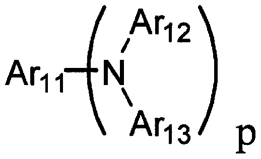
  • styrylamine compound and the styryldiamin compound those represented by the following general formula (a) are preferable.
  • Ar represents a phenyl group, a biphenyl group, a terphenyl group, a stilbene group, a distili group,
  • Ar and Ar are each a hydrogen atom or carbon.
  • An aromatic hydrocarbon group having a number of 6 to 20, Ar, Ar and Ar may be substituted .
  • p is an integer from 1 to 4, and p is preferably an integer from 1 to 2, among them. More preferably, at least one of Ar and Ar is substituted with a styryl group.
  • examples of the aromatic hydrocarbon group having 6 to 20 carbon atoms include a phenyl group, a naphthyl group, an anthranyl group, a phenanthryl group, and a terphenyl group.
  • aromatic amine compound and aromatic diamine compound those represented by the following general formula (b) are preferable.
  • q is an integer from:! to 4, among which q is preferably an integer from:! to 2.
  • examples of the aryl group having 5 to 40 nuclear carbon atoms include a phenyl group, a naphthyl group, an anthranyl group, a phenanthryl group, a pyrenyl group, a coronyl group, a biphenyl group, a terphenyl group, Ryl group, furanyl group, thiophenyl group, benzothiophenyl group, oxadiazolyl group, diphenylanthranyl group, indolyl group, carbazolyl group, pyridinole group, benzoquinolyl group, fluoranthur group, acenaphthofluoranthur group, stilbene Group, perylenyl group, chrysenyl group, picenyl group, triphenylenyl group, rubicenyl group, benzoanthracenyl group, phenylanthranyl group, bisanthracenyl group, or the following general
  • an alkyl group having 1 to 6 carbon atoms (ethyl group, methinole group, i propyl group, n propyl group, s butynole group, t butyl group, pentinole group) Group, hexyl group, cyclopentyl group, cyclohexyl group, etc.), C1-C6 alkoxy group (ethoxy group, methoxy group, i propoxy group, n propoxy group, s butoxy group, t-butoxy group, pentoxy group) Group, hexyloxy group, cyclopentoxy group, cyclohexyloxy group, etc.), aryl group having 5 to 40 nuclear carbon atoms, amino group substituted with aryl group having 5 to 40 nuclear carbon atoms, nuclear carbon number 5 Examples include an ester group having a ⁇ 40 aryl group, an ester group having an alkyl group
  • Examples of the condensed polycyclic aromatic compound include naphthalene, anthracene, phenanthrene, pyrene, coronene, biphenylenole, terfeninole, pyromononore, furan, thiophene, benzothiophene, oxadiazole, indole, Condensed polycyclic aromatic compounds such as carbazole, pyridine, benzoquinoline, fluoranthenine, benzofluoranthene, acenaphthofluoranthenine, stilbene, perylene, taricene, picene, triphenylenine, norevicene, benzoanthracene, etc. preferable.
  • the phosphorescent dopant is preferably a metal complex compound containing at least one metal selected from the group consisting of Ir, Ru, Pd, Pt, Os, and Re. It preferably has at least one skeleton selected from the group consisting of a phenyl pyridine skeleton, a bibilidinole skeleton, and a phenantorin phosphorus skeleton.
  • metal complexes include tris (2-phenylpyridine) iridium, tris (2-phenylpyridine) ruthenium, tris (2-phenylpyridine) palladium, bis (2-phenylpyridine) platinum, Tris (2-phenyl pyridine) osmium, Tris (2-phenyl pyridine) rhenium, Otaethyl platinum vorphyrin, Octaphenyl platinum porphyrin, Ottaethyl palladium porphyrin, Ottaf Strengths such as ⁇ nylpalladium porphyrins and the like are not limited to these, and an appropriate complex is selected from the relationship with the required emission color, device performance, and host compound.
  • the organic EL device of the present invention is a device in which one or more organic thin film layers are formed between an anode and a cathode.
  • a light emitting layer is provided between the anode and the cathode. The light emitting layer
  • a hole injection material or an electron injection material may be included to transport holes injected from the anode or electrons injected from the cathode to the light emitting material in addition to the light emitting material.
  • the light emitting material has a very high fluorescence quantum efficiency, a high hole transport capability and an electron transport capability, and forms a uniform thin film.
  • Multi-layer type organic EL devices are (Anode / Hole injection layer Z Light emitting layer Z Cathode), (Anode / Light emitting layer)
  • Electron injection layer / cathode Electron injection layer / cathode
  • anode / hole injection layer / light emitting layer / electron injection layer / cathode Electron injection layer / cathode
  • a further known light emitting material, doping material, and hole injection are added to the light emitting layer as necessary.
  • Materials and electronic injection materials can also be used.
  • a doping material any of heavy metal complexes represented by phosphorescent iridium can be used in addition to conventional fluorescent materials.
  • the organic EL element can be prevented from deteriorating brightness and life due to quenching by using a multilayer structure. If necessary, a light emitting material, another doping material, a hole injection material, and an electron injection material can be used in combination. In addition, with other doping materials, the luminance and luminous efficiency can be improved, and red and white light emission can be obtained.
  • the hole injection layer, the light emitting layer, and the electron injection layer may each be formed of two or more layers.
  • the layer that injects holes from the electrode is a hole injection layer
  • the layer that receives holes from the hole injection layer and transports holes to the light emitting layer is a hole transport layer.
  • an electron injection layer a layer that injects electrons from an electrode
  • a layer that receives electrons from the electron injection layer and transports electrons to a light emitting layer is referred to as an electron transport layer.
  • each of these layers is selected and used depending on factors such as the energy level of the material, heat resistance, adhesion with the organic thin film layer or the metal electrode.
  • Examples of the light-emitting material or host material that can be used in the light-emitting layer together with the compounds of the general formulas (1) to (6) include anthracene, naphthalene, phenanthrene, pyrene, tetracene, coronene, taricene, fluorescein, perylene, and lid-open perylene.
  • the hole injecting / transporting material has the ability to transport holes, has a hole injecting effect from the anode, an excellent hole injecting effect for the light emitting layer or the light emitting material, and the light emitting layer.
  • a compound that prevents the exciton produced in step 1 from moving to the electron injection layer or the electron injection material and has an excellent thin film forming ability is preferable.
  • phthalocyanine derivatives naphthalocyanine derivatives, porphyrin derivatives, oxazole, oxadiazole, triazole, imidazole, imidazolone, imidazolethione, pyrazoline, pyrazolone, tetrahydroimidazole, oxazole, oxadiazole, hydrazone, and acylhydrazone, Polyarylalkane, stilbene, butadiene, benzidine type triphenylamine, styrinoleamine type triphenylamine, diamine type triphenylamine, and their derivatives, and polymer materials such as polycarbcarbazole, polysilane, and conductive polymers.
  • the powers listed are not limited to these.
  • hole injection / transport materials that can be used in the organic EL device of the present invention, more effective materials are aromatic tertiary amine derivatives or phthalocyanine derivatives.
  • aromatic tertiary amine derivatives include triphenylamine, tritolylamine, tolyldiphenylamine, ⁇ , ⁇ '-diphenyl-1-N, ⁇ , mono (3-methylphenyl) -1,1,1,1-biphenyl 4, 4 '—diamin, ⁇ , ⁇ , ⁇ ', ⁇ '— (4-methylphenyl) 1 1, 1 '-phenyl —4, 4, 1 diamin, ⁇ , ⁇ , ⁇ , ⁇ , 1 ( 4-methylphenyl) 1, 1 '-biphenyl 1 4, 4'-diamin, ⁇ , ⁇ '-diphenyl 1 ⁇ , ⁇ '-dinaphthyl 1, 1' -biphenyl 1 4 , 4, 1, Diamine, ⁇ , ⁇ ,-(Methylphenyl) ⁇ , N '-(4— ⁇ Butylphenyl)-Phenylanthrene 9, 10-Diamine
  • phthalocyanine (p c ) derivatives are H2 Pc, CuPc, CoPc, NiPc, ZnPc, Pd Pc, FePc, MnPc, ClAlPc, ClGaPc, CllnPc, ClSnPc, C12 SiPc, (HO) AlPc, (HO) GaPc, Forces that are phthalocyanine derivatives and naphthalocyanine derivatives such as VOPc, TiOPc, MoOPc, GaPc_O_GaPc, but are not limited thereto.
  • the electron injection / transport material has the ability to transport electrons, has an electron injection effect from the cathode, and has an excellent electron injection effect on the light emitting layer or the light emitting material.
  • a compound that prevents migration of the element to the hole injection layer and has an excellent thin film forming ability is preferred.
  • Specific examples include fluorenone, anthraquinodimethane, diphenoquinone, thiopyrandioxide, oxazole, oxadiazole, triazole, imidazole, perylenetetracarboxylic acid, fluorenylidenemethane, anthraquinodimethane, anthrone, and their derivatives. Power It is not limited to these.
  • the charge injection property can be improved by adding an electron accepting material to the hole injecting material and an electron donating material to the electron injecting material.
  • a more effective electron injection material is a metal complex compound or a nitrogen-containing five-membered ring derivative.
  • metal complex compounds include 8-hydroxyquinolinate tritium, bis (8-hydroxyquinolinato) zinc, bis (8-hydroxyquinolinato) copper, bis (8-hydroxyquinolinato) manganese, tris ( 8-hydroxyquinolinate) aluminum, tris (2-methyl- 1-8 -hydroxyquinolinate) aluminum, tris ( 8 -hydroxyquinolinato) gallium, bis
  • oxazole, thiazole, oxadiazole, thiadiazole or triazole derivative is preferred as the nitrogen-containing five-membered derivative.
  • a light emitting material in addition to the light emitting material represented by the general formulas (1) to (6), a light emitting material, a doping material, a hole injection material, and an electron injection At least one of the materials may be contained in the same layer.
  • a protective layer is provided on the surface of the element, or the entire element is protected by silicon oil, resin, etc. It is also possible.
  • the conductive material used for the anode of the organic EL element a material having a work function larger than 4 eV is suitable, and carbon, aluminum, vanadium, iron, cobalt, nickel, tandasten, silver, gold, Platinum, palladium, etc. and their alloys, metal oxides such as tin oxide and indium oxide used for ITO substrates and NESA substrates, and organic conductive resins such as polythiophene and polypyrrole are used.
  • the conductive material used for the cathode those having a work function smaller than 4 eV are suitable.
  • Examples of the alloy include magnesium Z silver, magnesium Z indium, lithium / aluminum, and the like. Representative examples thereof are not limited to these.
  • the ratio of the alloy is controlled by the temperature of the deposition source, the atmosphere, the degree of vacuum, etc., and is selected to an appropriate ratio.
  • the anode and the cathode may be formed with a layer structure of two or more layers.
  • the substrate is also preferably transparent.
  • the transparent electrode is set using the conductive material described above so as to ensure a predetermined translucency by a method such as vapor deposition or sputtering.
  • the electrode on the light emitting surface should have a light transmittance of 10% or more.
  • the substrate is not limited as long as it has mechanical and thermal strength and is transparent, but includes a glass substrate and a transparent resin film. Examples of transparent resin films include polyethylene, ethylene-butyl acetate copolymer, ethylene-butyl alcohol copolymer, polypropylene, polystyrene, polymethyl metatalylate, polychlorinated butyl, and polybular alcohol.
  • Polyurethane polybutyl butyral, nylon, polyether ether ketone, polysulfone, polyether sulfone, tetrafluoroethylene-perfluoroalkyl vinyl ether copolymer, polyvinyl fluoride, tetrafluoroethylene monoethylene Copolymer, Tetrafluoroethylene monohexafluoropropylene copolymer, Polychlorinated trifluorinated ethylene, Polyvinylidene fluoride, Polyester, Polycarbonate, Polyurethane, Polyimide, Polyetherimide, Polyimide, Polypropylene, etc. .
  • each layer of the organic EL device according to the present invention is performed by a dry film formation method such as vacuum deposition, sputtering, plasma, ion plating, or a wet film formation method such as spin coating, dating, or flow coating.
  • a deviation method can be applied.
  • the film thickness is not particularly limited, but should be set to an appropriate film thickness. If the film thickness is too thick, a large applied voltage is required to obtain a constant light output, resulting in poor efficiency. If the film thickness is too thin, pinholes and the like are generated, and sufficient light emission luminance cannot be obtained even when an electric field is applied.
  • a typical film thickness is in the range of 5 nm to 10 zm.
  • a force in the range of 10 nm force to 0.2 xm is even more preferred.
  • the power for forming a thin film by dissolving or dispersing the material forming each layer in an appropriate solvent such as ethanol, chloroform, tetrahydrofuran, dioxane or the like may be used.
  • An appropriate resin or additive may be used for improving film formability and preventing pinholes in the film.
  • Resins that can be used include insulating resins such as polystyrene, polycarbonate, polyarylate, polyester, polyamide, polyurethane, polysulfone, polymethyl methacrylate, polymethyl acrylate, cellulose, and copolymers thereof, poly _N_ Examples thereof include photoconductive resins such as bull force novasol and polysilane, and conductive resins such as polythiophene and polypyrrole. Examples of additives include antioxidants, ultraviolet absorbers, and plasticizers.
  • the organic EL device of the present invention can be used as a flat light emitter such as a flat panel display of a wall-mounted television, a copying machine, a printer, a light source such as a backlight of a liquid crystal display or instruments, a display board, a marker lamp, and the like.
  • anthracene synthesized in a conventional manner with the obtained intermediate A The derivative boronic acid was reacted with Suzuki coupling reaction to obtain the target compound (H_1). The details are described below.
  • Example 1 Manufacture of organic EL elements' evaluation
  • a glass substrate with a 25 mm ⁇ 75 mm ⁇ l. 1 mm thick IT ⁇ transparent electrode (Zomatic Co., Ltd.) was ultrasonically cleaned in isopropyl alcohol for 5 minutes, followed by UV ozone cleaning for 30 minutes.
  • the glass substrate with the transparent electrode line after cleaning is mounted on the substrate holder of the vacuum deposition apparatus, and first, the transparent electrode is covered on the surface where the transparent electrode line is formed so that the film thickness becomes 60 nm.
  • ⁇ , N, 1bis (N, N, 1-diphenyl) _4-aminophenyl, 1-N, N-diphenyl-1, 4'-diamino-1, 1, 1-biphenyl (hereinafter “TP”) Abbreviated as “D232 membrane”.
  • This TPD232 film functions as a hole injection layer.
  • an N, N, ⁇ ′, N′-tetra (4-biphenyl) -diaminobiphenylene layer (hereinafter abbreviated as “TBDB layer”) was formed to a thickness of 20 nm.
  • This membrane functions as a hole transport layer.
  • a compound (H_l) was deposited as a light emitting material (host material) so as to have a film thickness of 40 nm.
  • This film functions as a light emitting layer.
  • An Alq film having a thickness of 10 nm was formed on this film. This functions as an electron injection layer.
  • Li Li source: manufactured by SAES Getter
  • Alq Alq
  • metal A1 was deposited to form a metal cathode, thereby forming an organic EL device.
  • Table 1 shows the results of the evaluation of the following (1) and (2) using the obtained organic EL device.
  • Example 1 an organic EL device was produced in the same manner except that the compound shown in Table 1 was used as the light emitting material (host material) instead of the compound (H-l), and the results of the evaluation were shown. Shown in 1.
  • Example 1 an organic EL device was manufactured in the same manner except that the comparative compounds 1 to 3 shown in Table 1 were used instead of the compound (H_1) as the light emitting material (host material). Table 1 shows the evaluation results.
  • the organic EL device using the silicon compound of the present invention as a material for an organic EL device has a long lifetime with high luminous efficiency and high color purity. For this reason, it is extremely useful as a highly practical blue organic EL device. It is also extremely useful when applied to white organic EL devices.

Landscapes

  • Chemical & Material Sciences (AREA)
  • Organic Chemistry (AREA)
  • Engineering & Computer Science (AREA)
  • Materials Engineering (AREA)
  • Physics & Mathematics (AREA)
  • Spectroscopy & Molecular Physics (AREA)
  • Optics & Photonics (AREA)
  • Inorganic Chemistry (AREA)
  • Electroluminescent Light Sources (AREA)
  • Organic Low-Molecular-Weight Compounds And Preparation Thereof (AREA)

Abstract

 置換シリル基を有する特定構造のケイ素化合物、並びに、陰極と陽極間に少なくとも発光層を含む一層又は複数層からなる有機薄膜層が挟持されている有機エレクトロルミネッセンス素子であって、該有機薄膜層の少なくとも一層が、前記ケイ素化合物を単独もしくは混合物の成分として含有する有機エレクトロルミネッセンス素子であり、発光効率が高く、色純度が高く、長寿命な発光が得られる有機エレクトロルミネッセンス素子及びそれを実現する新規なケイ素化合物を提供する。

Description

明 細 書
ケィ素含有化合物及びそれを利用した有機エレクト口ルミネッセンス素子 技術分野
[0001] 本発明は、ケィ素含有化合物及びそれを利用した有機エレクト口ルミネッセンス (E L)素子に関し、特に、発光効率が高ぐ色純度が高ぐ長寿命な有機 EL素子及びそ れを実現するケィ素含有化合物に関するものである。
背景技術
[0002] 有機 EL素子は、電界を印加することにより、陽極より注入された正孔と陰極より注 入された電子の再結合エネルギーにより蛍光性物質が発光する原理を利用した自 発光素子である。イーストマン 'コダック社の C. W. Tang等による積層型素子による 低電圧駆動有機 EL素子の報告(C. W. Tang, S. A. Vanslyke,アプライドフィジックス レターズ (Applied Physics Letters) , 51卷、 913頁、 1987年等)がなされて以来、有 機材料を構成材料とする有機 EL素子に関する研究が盛んに行われている。 Tang 等は、トリス(8—ヒドロキシキノリノールアルミニウム)を発光層に、トリフエ二ルジァミン 誘導体を正孔輸送層に用いている。積層構造の利点としては、発光層への正孔の注 入効率を高めること、陰極より注入された電子をブロックして再結合により生成する励 起子の生成効率を高めること、発光層内で生成した励起子を閉じ込めること等が挙 げられる。この例のように有機 EL素子の素子構造としては、正孔輸送 (注入)層、電 子輸送性発光層の二層型、又は正孔輸送 (注入)層、発光層、電子輸送 (注入)層の 3層型等がよく知られている。こうした積層型構造素子では注入された正孔と電子の 再結合効率を高めるため、素子構造や形成方法の工夫がなされている。
また、発光材料としてはトリス(8—キノリノラート)アルミニウム錯体等のキレート錯体 、クマリン誘導体、テトラフエニルブタジエン誘導体、ビススチリルァリーレン誘導体、 ォキサジァゾール誘導体等の発光材料が知られており、それからは青色から赤色ま での可視領域の発光が得られることが報告されており、カラー表示素子の実現が期 待されている(例えば、特許文献:!〜 3)。
[0003] また、最近では、燐光性化合物を発光材料として用レ、、三重項状態のエネルギー を EL発光に用いる検討が多くなされている。例えば、プリンストン大学のグループに より、イリジウム錯体を発光材料として用いた有機 EL素子が、高い発光効率を示すこ とが報告されている(非特許文献 1)。さらに、このような低分子材料を用いた有機 EL 素子の他にも、共役系高分子を用いた有機 EL素子が、ケンブリッジ大学のグループ (非特許文献 2)により報告されている。この報告ではポリフエ二レンビニレン (PPV)を 塗工系で成膜することにより、単層で発光を確認している。
このように有機 EL素子における最近の進歩は著しぐその特徴は低印加電圧で高 輝度、発光波長の多様性、高速応答性、薄型、軽量の発光デバイス化が可能である こと力ら、広汎な用途への可能性を示唆している。
有機発光素子における著しい進歩に伴い、発光材料に対する要求性能も高まって おり、特許文献 4及び特許文献 5には、フルオレンを連結基としたピレン化合物が開 示されている。また、特許文献 6には、置換シリル基を 2つ有するアントラセン化合物 が開示されているが、発光効率が低いなど問題点があり、さらなる高輝度の光出力あ るいは高変換効率が必要とされる発光材料に対する要求特性を満たすには至って いない。また、長時間の使用による経時変化や酸素を含む雰囲気気体や湿気などに よる劣化等の耐久性や、フルカラーディスプレイ等への応用を考慮した色純度の良 い青、緑、赤の発光への要求に対してまだ十分な有機 EL素子用材料、特に発光材 料は見出されていない。
特許文献 1 :特開平 8— 239655号公報
特許文献 2 :特開平 7— 138561号公報
特許文献 3:特開平 3— 200889号公報
特許文献 4:特開 2004— 83481号公報
特許文献 5:特開 2004— 43349号公報
特許文献 6:特開 2006 - 28175号公報
非特許文献 1 : Nature, 395, 151 (1998)
非特許文献 2 : Nature, 347, 539 (1990)
発明の開示
発明が解決しょうとする課題 [0005] 本発明は、前記の課題を解決するためになされたもので、発光効率が高ぐ色純度 が高ぐ長寿命な発光が得られる有機 EL素子及びそれを実現する新規なケィ素含 有化合物を提供することを目的とする。
課題を解決するための手段
[0006] 本発明者らは、前記目的を達成するために鋭意研究を重ねた結果、下記一般式(
1)で表される置換シリル基を有するケィ素含有化合物を有機 EL素子用材料として 用いることで前記の目的を達成することを見出し本発明を完成したものである。
なお、本発明において、ケィ素含有化合物という場合、以下で説明するケィ素含有 アントラセン誘導体及びケィ素含有ピレン誘導体も含む。
すなわち、本発明は、下記一般式(1)で表されるケィ素含有化合物において、 (1 1)、 (1 - 2) , (1 - 3) , (1 4)又は(1 5)の構成を有するケィ素含有化合物を 提供するものである。
[0007] [化 1]
Figure imgf000004_0001
[0008] {式中、 FAは置換もしくは無置換の核炭素数 8〜50の縮合環残基であり、 L〜L及
1 1 2 び Ar〜Arは、それぞれ独立に同一でも異なっていてもよぐ置換もしくは無置換の
1 6
核炭素数 6〜50の芳香族炭化水素基、置換もしくは無置換の核炭素数 3〜50の芳 香族複素環基、置換もしくは無置換の核炭素数 8〜50の縮合芳香族基、又は置換も しくは無置換の炭素数 1〜: 10のアルキル基である。 a、 b、 d及び eはそれぞれ 0〜6の 整数、 cは:!〜 6の整数であり、 a + e≥lである。
(1— 1)ただし、 FAがアントリレン基であり、かつ a = e = lである場合、 Lとしが同時
1 1 2 にフエ二レン基になる場合はなレ、。
(1— 2)ただし、 FAがアントリレン基又はナフチレン基であり、かつ a = e = lである場
1
合、 Lとしが同時にフエ二レン基になる場合はない。
1 2
(1— 3)ただし、 FAが核炭素数 8〜20の縮合環残基であり、かつ a = e = lである場 合、 Lとしが同時にフエ二レン基になる場合はない。
1 2
(1—4)ただし、 FAが核炭素数 8〜20の縮合環残基 [アントリレン基及びナフチレン
1
基を除く。 ]であり、かつ a = e = lである場合、 Lとしが同時にフエ二レン基になる。
1 2
(1— 5)ただし、 FAがピレニレン基であり、かつ a = e = lである場合、 Lとしが同時
1 1 2 にフエ二レン基になる。 }
[0009] また、本発明は、陰極と陽極間に少なくとも発光層を含む一層又は複数層からなる 有機薄膜層が挟持されている有機 EL素子であって、該有機薄膜層の少なくとも一層 が、前記ケィ素含有化合物を単独もしくは混合物の成分として含有する有機 EL素子 を提供するものである。
発明の効果
[0010] 本発明のケィ素含有化合物を有機 EL素子用材料として用いた有機 EL素子は、発 光効率が高ぐ色純度が高ぐ長寿命である。
発明を実施するための最良の形態
[0011] 本発明のケィ素含有化合物は、下記一般式(1)で表され、下記(1一 1)、 (1 - 2) ,
(1 - 3) , (1一 4)又は(1一 5)の構成を有する。
[化 2]
Figure imgf000005_0001
[0012] (l - l) FAがアントリレン基であり、かつ a = e = lである場合、 Lとしが同時にフエ二
1 1 2
レン基になる場合はない。
(1 - 2) FAがアントリレン基又はナフチレン基であり、かつ a = e = lである場合、 Lと
1 1
Lが同時にフエ二レン基になる場合はない。
2
(1 3) FAが核炭素数 8〜20の縮合環残基であり、かつ a = e = lである場合、 Lと
1 1
Lが同時にフエ二レン基になる場合はない。
2
(1— 4) FAが核炭素数 8〜20の縮合環残基 [アントリレン基及びナフチレン基を除く
1
。 ]であり、かつ a = e = lである場合、 Lとしが同時にフエ二レン基になる。
1 2 (1 - 5) FAがピレニレン基であり、かつ a = e = lである場合、 Lとしが同時にフエ二
1 1 2
レン基になる。
[0013] 一般式(1)において、 a及び eはそれぞれ 0〜6の整数であり、:!〜 4であると好ましく 、:!〜 2であるとさらに好ましレ、。 b及び dはそれぞれ 0〜6の整数であり、 0〜3であると 好ましぐ 0〜2であるとさらに好ましレ、。 cは:!〜 6の整数であり、:!〜 4であると好ましく 、:!〜 3であるとさらに好ましい。
また、 a + e≥lであり、:!〜 4であると好ましく、:!〜 2であるとさらに好ましい。
[0014] 本発明において、一般式(1)で表されるケィ素含有化合物は、下記一般式 (2) [前 記一般式(1)で a = b = c = d= lである]で表されるケィ素含有化合物であると好まし レ、。
[化 3]
Figure imgf000006_0001
( 2 )
[0015] 本発明において、一般式(1)で表されるケィ素含有化合物は、下記一般式 (3)〜( 6)のレ、ずれかで表されるケィ素含有化合物であると好ましレ、。
[化 4]
Figure imgf000006_0002
( 5 ) ( 6 )
[0016] 一般式(1)〜(6)において、 FA及び FAは置換もしくは無置換の核炭素数 8〜50
(好ましくは核炭素数 10〜36)の縮合環残基であり、この核炭素数 8〜50の縮合環 残基としては、例えば、ナフタレン、フエナントレン、ピレン、アントラセン、テトラセン、 コロネン、タリセン、フルオレン、ペリレン、ベンゾアントラセン、ペンタセン、ジベンゾァ ントラセン、ベンゾピレン、ベンゾフノレ才レン、フノレ才ランテン、ベンゾフノレ才ランテン、 ナフチルフルオランテン、ジベンゾフルオレン、ジベンゾピレン、ジベンゾフルオラン テン、ナフタセン、ァセナフチルフルオランテン、ベンツアントラセン、ベンツフルォレ ン、フルォレセイン、フタ口ペリレン、ナフタ口ペリレン、ペリノン、フタ口ペリノン、ナフタ 口ペリノン、ジフヱニルブタジエン、テトラフヱニルブタジエン、クマリン、ォキサジァゾ ール、アルダジン、ビスベンゾキサゾリン、ビススチリル、ピラジン、シクロペンタジェン 、ィミン、ジフエニルェチレン、ビュルアントラセン、ジァミノカルバゾール、ピラン、チ ォピラン、ポリメチン、メロシアニン、イミダゾールキレート化合物、ォキシノイド化合物 、キナクリドン、ルブレン、スチルベン系誘導体及び下記構造を有する蛍光色素等挙 の骨格を有する化合物の残基が挙げられ、そのなかでもナフタレン、フエナントレン、 ピレン、アントラセン、テトラセン、コロネン、タリセン、フルオレン、ペリレン、ベンゾアン トラセン、ペンタセン、ジベンゾアントラセン、ベンゾピレン、ベンゾフルオレン、フルォ ランテン、ベンゾフルオランテン、ナフチルフルオランテン、ジベンゾフルオレン、ジべ ンゾピレン、ジベンゾフルオランテン、ナフタセン、又はァセナフチルフルオランテン 骨格を有する化合物の残基が好ましぐピレン、アントラセン、フルオランテン骨格を 有する化合物の残基が好ましぐアントラセン又はピレン骨格を有する化合物の残基 が特に好ましい。
[0017] 一般式(1)の(1 1)の構造において、 FAで表される核炭素数 8〜50の縮合環残
1
基が、アントラセンの骨格を有する化合物の残基である(ただし、 a = e = lである場合 、 Lとしが同時にフエ二レン基になる場合はない。)と好ましぐ前記一般式(2)〜(6)
1 2
のいずれかの FA及び/又は FAで表される核炭素数 8〜50の縮合環残基力 ァ
1 2
ントラセンの骨格を有する化合物の残基である(ただし、前記一般式(2)で Lとしが
1 2 同時にフエ二レン基になる場合はなレ、。 )と好ましい。
[0018] 一般式(1)の(1一 3)の構造において、前記一般式(1)の FAで表される核炭素数
1
8〜50の縮合環残基が、ピレンの骨格を有する化合物の残基である(ただし、 a = e = 1である場合、 Lとしが同時にフヱニレン基になる場合はない。)と好ましぐ前記一 般式(2)〜(6)のレ、ずれかの FA及び/又は FAで表される核炭素数 8〜50の縮合
1 2
環残基が、ピレンの骨格を有する化合物の残基である(ただし、前記一般式(2)で L
1 としが同時にフエ二レン基になる場合はない。)と好ましい。
2
[0019] 一般式(1)の(1一 5)の構造において、前記一般式(1)の FAで表される核炭素数
1
8〜50の縮合環残基が、ピレンの骨格を有する化合物の残基である(ただし、 a = e = 1である場合、 Lとしが同時にフヱニレン基になる。)と好ましぐ前記一般式(2)〜
1 2
(6)のいずれかの FA及び/又は FAで表される核炭素数 8〜50の縮合環残基力
1 2
ピレンの骨格を有する化合物の残基である(ただし、前記一般式(2)で Lとしが同時
1 2 にフエ二レン基になる。)と好ましい。
[0020] このような骨格を有する好ましい構造を例示すると以下のものが挙げられる。
[化 5]
Figure imgf000009_0001
Figure imgf000009_0002
また、ピレン骨格を有する構造を例示すると以下のものが挙げられる。
[化 6] [ oo]
Figure imgf000010_0001
6
l76S0/.00Zdf/X3d
Figure imgf000011_0001
[0023] [化 8]
Figure imgf000012_0001
一般式(1)〜(6)において、 L〜L及び Ar〜Arは、それぞれ独立に、同一でも
1 2 1 6
異なっていてもよぐ置換もしくは無置換の核炭素数 6〜 50 (好ましくは核炭素数 6〜 36)の芳香族炭化水素基、置換もしくは無置換の核炭素数 3〜50 (好ましくは核炭 素数 3〜36)の芳香族複素環基、置換もしくは無置換の核炭素数 8〜50 (好ましくは 核炭素数 10〜36)の縮合芳香族基、又は置換もしくは無置換の炭素数 1〜: 10 (好ま しくは炭素数 1〜4)のアルキル基である。
L 〜L及び Ar〜Arで表される核炭素数 8〜 50の縮合芳香族基としては、 FA及
1 2 1 6 1 び FAで表される核炭素数 8〜50の縮合環残基と同様の例が挙げられる。
2
[0025] L 〜L及び Ar〜Arで表される核炭素数 6〜50の前記芳香族炭化水素基として
1 2 1 6
は、例えば、フエニル基、ナフチル基(1—ナフチル基、 2 _ナフチル基)、アントリル 基(1—アントリル基、 2 アントリノレ基、 9 _アントリル基)、フエナントリル基(1—フエ ナントリル基、 2—フエナントリル基、 3—フエナントリル基、 4—フエナントリル基、 9 _ フエナントリル基)、ナフタセニル基(1—ナフタセニル基、 2_ナフタセニル基、 9—ナ フタセニル基)、ピレニル基(1—ピレニル基、 2—ピレニル基、 4—ピレニル基)、ビフ ェニルイル基(2—ビフエ二ルイル基、 3—ビフエ二ルイル基、 4—ビフエ二ルイル基)、 ターフェ二ルーィル基(p—ターフェ二ルー 4ーィル基、 p—ターフェ二ルー 3—ィル基 、 p ターフェニノレー 2—ィノレ基、 m ターフェニノレー 4ーィノレ基、 m ターフェ二ノレ —3—ィル基、 m—ターフェ二ノレ— 2—ィル基)、トリル基(o トリル基、 m トリル基、 ρ—トリル基)、ブチルフエニル基(p—t ブチルフエニル基)、 p— (2—フエニルプロ ピル)フエニル基、メチルーナフチル基(3—メチルー 2 ナフチル基、 4ーメチノレー 1 —ナフチル基)、メチル—アントリル基(4—メチル— 1—アントリル基)、メチルビフエ二 ノレィル基(4'ーメチルビフエ二ルイル基)、ブチルーターフエ二ルーィル基(4" t— プチルー p—ターフェ二ルー 4ーィル基)等が挙げられる。好ましくはフエニル基、ナ フチル基、ピレニル基である。
[0026] L 〜L及び Ar〜Arで表される核炭素数 6〜50の前記芳香族複素環基としては、
1 2 1 6
例えば、ピロリル基(1—ピロリル基、 2_ピロリル基、 3 _ピロリル基)、ピラジュル基、 ピリジニル基(2 _ピリジニル基、 3 _ピリジニル基、 4_ピリジニル基)、インドリル基(1 —インドリル基、 2_インドリル基、 3_インドリル基、 4_インドリル基、 5_インドリル基 、 6 _インドリノレ基、 7_インドリル基)、イソインドリル基(1—イソインドリル基、 2_イソ インドリル基、 3 _イソインドリル基、 4 _イソインドリル基、 5 _イソインドリル基、 6—ィ ソインドリル基、 7_イソインドリル基)、フリル基(2_フリル基、 3 _フリル基)、ベンゾ フラニル基(2 べンゾフラニル基、 3 べンゾフラニル基、 4一べンゾフラニル基、 5 一べンゾフラニル基、 6—べンゾフラニル基、 7—べンゾフラニル基)、イソベンゾフラ ニル基(1 イソべンゾフラニル基、 3—イソべンゾフラニル基、 4 イソべンゾフラニル 基、 5 _イソべンゾフラニル基、 6 _イソべンゾフラニル基、 7 _イソべンゾフラニル基) 、キノリノレ基(2—キノリノレ基、 3—キノリノレ基、 4一キノリノレ基、 5—キノリノレ基、 6—キノ リル基、 7—キノリノレ基、 8 _キノリル基)、イソキノリル基(1—イソキノリル基、 3_イソキ ノリル基、 4_イソキノリル基、 5_イソキノリル基、 6 _イソキノリノレ基、 7_イソキノリノレ 基、 8_イソキノリル基)、キノキサリニル基(2—キノキサリニル基、 5_キノキサリニノレ 基、 6 _キノキサリニル基)、カルバゾリル基(1 _カルバゾリル基、 2_カルバゾリル基 、 3_カノレバゾリノレ基、 4_カノレバゾリノレ基、 9 _カルバゾリル基)、フエナンスリジニル 基(1—フエナンスリジニル基、 2—フエナンスリジニル基、 3—フエナンスリジニル基、 4—フエナンスリジニル基、 6—フエナンスリジニル基、 7—フエナンスリジニル基、 8_ フエナンスリジニル基、 9 フエナンスリジニル基、 10—フエナンスリジニル基)、アタリ ジニル基(1—アタリジニル基、 2—アタリジニル基、 3—アタリジニル基、 4—アタリジニ ル基、 9—アタリジニル基)、フエナンスロリン一ィル基(1 , 7 フエナンスロリン一 2— イノレ基、 1 , 7—フエナンスロリン 3—ィノレ基、 1 , 7—フエナンスロリン 4ーィノレ基、 1 , 7—フエナンスロリンー5—ィノレ基、 1 , 7—フエナンスロリンー6—ィノレ基、 1, 7—フ ェナンスロリン一 8—ィル基、 1 , 7—フエナンスロリン一 9—ィル基、 1 , 7—フエナンス 口リン一 10—イノレ基、 1 , 8 フエナンスロリン一 2—イノレ基、 1 , 8 フエナンスロリン一 3—ィノレ基、 1 , 8—フエナンスロリン 4ーィノレ基、 1, 8—フエナンスロリン 5—ィノレ 基、 1 , 8—フエナンスロリン一 6—イノレ基、 1, 8—フエナンスロリン一 7—イノレ基、 1, 8 —フエナンスロリン _ 9—ィノレ基、 1 , 8_フエナンスロリン一10—ィノレ基、 1, 9 _フエ ナンスロリン一 2—ィル基、 1, 9—フエナンスロリン一 3—ィル基、 1 , 9—フエナンスロ リン _4—ィノレ基、 1, 9_フエナンスロリン _ 5—ィノレ基、 1 , 9_フエナンスロリン _ 6 —ィル基、 1 , 9—フエナンスロリン一 7—ィル基、 1, 9—フエナンスロリン一 8—ィル基 、 1 , 9—フエナンスロリン一 10—ィル基、 1, 10—フエナンスロリン一 2—ィル基、 1 , 1 0_フエナンスロリン _ 3—ィノレ基、 1 , 10—フエナンスロリン _4—ィノレ基、 1, 10—フ ェナンスロリン一 5—ィル基、 2, 9—フエナンスロリン一 1—ィル基、 2, 9—フエナンス 口リン一 3—ィル基、 2, 9 フエナンスロリン一 4—ィル基、 2, 9 フエナンスロリン一 5 ーィル基、 2, 9 フエナンスロリンー6—ィル基、 2, 9 フエナンスロリンー7 ィル基 、 2, 9 フエナンスロリン一 8—ィル基、 2, 9 フエナンスロリン一 10—ィル基、 2, 8 —フエナンスロリン一 1—ィノレ基、 2, 8_フエナンスロリン一 3—ィノレ基、 2, 8 _フエナ ンスロリン一 4 ィル基、 2, 8 フエナンスロリン一 5 ィル基、 2, 8 フエナンスロリン —6 ィル基、 2, 8 フエナンスロリン一 7 ィル基、 2, 8 フエナンスロリン一 9 ィ ノレ基、 2, 8 フエナンスロリン一 10 ィル基、 2, 7 フエナンスロリン一 1—ィル基、 2 , 7_フエナンスロリン一 3—ィノレ基、 2, 7_フエナンスロリン一 4—ィノレ基、 2, 7_フエ ナンスロリン一 5 ィル基、 2, 7 フエナンスロリン一 6 ィル基、 2, 7 フエナンスロ リン一 8 ィル基、 2, 7 フエナンスロリン一 9 ィル基、 2, 7 フエナンスロリン一 10 —ィル基)、フエナジニル基(1—フエナジニル基、 2—フエナジニル基)、フエノチアジ ニル基(1—フエノチアジニル基、 2—フエノチアジニル基、 3 _フヱノチアジニル基、 4 —フエノチアジニル基、 10—フエノチアジニル基)、フエノキサジニル基(1—フエノキ サジニル基、 2 フエノキサジニル基、 3 フエノキサジニル基、 4 フエノキサジニル 基、 10—フエノキサジニル基)、ォキサゾリル基(2—ォキサゾリル基、 4 ォキサゾリ ル基、 5 ォキサゾリル基、 2 ォキサジァゾリル基、 5 ォキサジァゾリル基)、フラザ ニル基(3 フラザニル基)、チェニル基(2 チェニル基、 3 チェニル基)、メチル ピロ一ルーィル基(2 メチルピロ一ルー 1ーィル基、 2 メチルピロ一ルー 3—ィル 基、 2 メチルピロ一ルー 4ーィル基、 2 メチルピロ一ルー 5—ィル基、 3—メチルビ ロール 1ーィル基、 3 メチルピロ一ルー 2—ィル基、 3 メチルピロ一ルー 4ーィル 基、 3 メチルピロ一ルー 5—ィル基)、ブチルピロ一ルーィル基(2— t ブチルピロ ール _4—ィル基)、 3- (2—フエニルプロピル)ピロール— 1—ィル基、メチル—イン ドリル基(2 メチル _ 1 _インドリル基、 4_メチル_ 1 _ィンドリル基、 2_メチル _ 3 —インドリル基、 4 _メチル _ 3 _インドリル基)、ブチル—インドリル基(2_t_ブチル _ 1 _インドリル基、 4_セ_ブチル_ 1 _ィンドリル基、 2_ _ブチル_ 3_ィンドリノレ 基、 4_t_ブチル _ 3 _インドリル基)等が挙げられる。好ましくはピリジル基、ピリミジ ル基である。
本発明の一般式(1)で表されるケィ素含有化合物は、下記部分構造 (A)が、下記 一般式(7)の残基又は一般式(8)の残基であるケィ素含有アントラセン誘導体である と好ましい。
[化 9]
Figure imgf000016_0001
Figure imgf000016_0002
[0028] [一般式(7)において、 Xは、それぞれ独立に同一でも異なっていてもよぐ単結合、 水素原子、置換もしくは無置換の核炭素数 6〜50の芳香族炭化水素基、置換もしく は無置換の核炭素数 5〜50の芳香族複素環基、置換もしくは無置換の炭素数 1〜5 0のァノレキノレ基、置換もしくは無置換の炭素数 3〜50のシクロアルキル基、置換もしく は無置換の炭素数 1〜50のアルコキシ基、置換もしくは無置換の炭素数 6〜50のァ ラルキル基、置換もしくは無置換の炭素数 5〜50のァリールォキシ基、置換もしくは 無置換の炭素数 5〜50のァリールチオ基、置換もしくは無置換の炭素数 1〜50のァ ルコキシカルボニル基、置換もしくは無置換のシリル基、カルボキシル基、ハロゲン原 子、シァノ基、ニトロ基、ヒドロキシル基である。
Ar及び Arは、それぞれ独立に同一でも異なっていてもよぐ置換もしくは無置換 の核炭素数 6〜 50の芳香族炭化水素基または置換もしくは無置換の核炭素数 8〜 5 0の縮合芳香族基であり、核炭素数 8〜50の縮合芳香族基である場合は、下記一般 式(B)で表される 1 ナフチル基又は下記一般式(C)で表される 2—ナフチル基で ある。ただし、前記一般式(1)において a = e = lである場合、 Arがフエ二レン基にな る場合はない。
[0029] [化 10]
Figure imgf000017_0001
(式中、 ^〜R7は、それぞれ独立に同一でも異なっていてもよぐ単結合、水素原子 又は置換もしくは無置換の炭素数 1〜50のアルキル基である。 )
f、 g、 hはそれぞれ 0〜4の整数であり、 iは 1〜3の整数である。また iが 2以上の場合 は、 [ ]内の基はそれぞれ独立に同一でも異なっていてもよい。 ]
[化 11]
Figure imgf000017_0002
[一般式(8)において、 A1及び A2は、それぞれ独立に同一でも異なっていてもよぐ 置換もしくは無置換の核炭素数 6〜50の芳香族炭化水素基で又は置換もしくは無 置換の核炭素数 8〜50の縮合芳香族基ある。
Ar及び Ar は、それぞれ独立に同一でも異なっていてもよぐ単結合、水素原子、
9 10
置換もしくは無置換の核炭素数 6〜50の芳香族炭化水素基、又は置換もしくは無置 換の核炭素数 8〜50の縮合芳香族基である。
RU〜R2°は、それぞれ独立に同一でも異なっていてもよぐ単結合、水素原子、置 換もしくは無置換の核炭素数 6〜50の芳香族炭化水素基、置換もしくは無置換の核 原子数 5〜50の芳香族複素環基、置換もしくは無置換の炭素数:!〜 50のアルキル 基、置換もしくは無置換の炭素数 3〜50のシクロアルキル基、置換もしくは無置換の 炭素数 1〜50のアルコキシ基、置換もしくは無置換の炭素数 6〜50のァラルキル基 、置換もしくは無置換の炭素数 5〜50のァリールォキシ基、置換もしくは無置換の炭 素数 5〜50のァリールチオ基、置換もしくは無置換の炭素数 1〜50のアルコキシ力 ルポ二ル基、置換もしくは無置換のシリル基、カルボキシル基、ハロゲン原子、シァノ 基、ニトロ基、ヒドロキシル基である。
Ar、 Ar 、 R19及び R2°は、それぞれ複数であってもよい。
9 10
ただし、前記一般式(1)で a = e = lの場合は一般式 (8)において、中心のアントラ センの 9位及び 10位に、該アントラセン上に示す X—Y軸に対して対称型となる基が 結合する場合はない。 ]
[0032] また、本発明の一般式(1)で表されるケィ素含有化合物における(1 _ 3)、 (1 - 5) の場合には、それぞれ、上記部分構造 (A)が、下記一般式(9)の残基において、 (9 _ 1)、(9— 2)の構造を有するケィ素含有ピレン誘導体であると好ましい。
[化 12]
Figure imgf000018_0001
[0033] [一般式(9)において、 L、 L'及び Ar、 Ar'は、それぞれ独立に同一でも異なってい てもよぐ単結合、水素原子、置換もしくは無置換の核炭素数 6〜50の芳香族炭化 水素基、置換もしくは無置換の核原子数 5〜50の芳香族複素環基、置換もしくは無 置換の核炭素数 8〜50の縮合芳香族基、置換もしくは無置換の炭素数 1〜50のァ ルキル基、置換もしくは無置換の炭素数 3〜50のシクロアルキル基、置換もしくは無 置換の炭素数 1〜50のアルコキシ基、置換もしくは無置換の炭素数 6〜50のァラル キル基、置換もしくは無置換の炭素数 5〜50のァリールォキシ基、置換もしくは無置 換の炭素数 5〜50のァリールチオ基、置換もしくは無置換の炭素数 1〜50のアルコ キシカルボニル基、置換もしくは無置換のシリル基、カルボキシル基、ハロゲン原子、 シァノ基、ニトロ基、ヒドロキシル基である。
mおよび sは 0〜2の整数、 nおよび tは 0〜4の整数である。
また、 L又は Arは、ピレンの 1〜5位のいずれかに結合し、 L'又は Ar,は、ピレンの 6〜: 10位のいずれかに結合する。
さらに、ピレンの 1〜5位に結合した(L) _Ar、ピレンの 6〜10位に結合した(L,) _Ar'は、それぞれ独立に同一でも異なっていてもよい。
[0034] (9_ 1)ただし、前記一般式(1)で a = e = lの場合、一般式(9)において、(L) -Ar m と(L' ) -Ar'が同時にフエ二レン基になる場合はない。
[0035] (9— 2)ただし、前記一般式(1)で a = e = lの場合、一般式(9)において(L) _Arと
(L' ) _Ar'が同時にフエ二レン基になる。 ]
[0036] 一般式(1)〜(9)の示す各基の置換基としては、例えば、アルキル基 (メチル基、ェ チノレ基、プロピル基、イソプロピル基、 n ブチル基、 s ブチル基、イソブチル基、 t ブチル基、 n ペンチル基、 n へキシル基、 n—へプチル基、 n—ォクチル基、ヒ ドロキシメチル基、 1ーヒドロキシェチル基、 2—ヒドロキシェチル基、 2—ヒドロキシイソ ブチル基、 1, 2—ジヒドロキシェチル基、 1 , 3—ジヒドロキシイソプロピル基、 2, 3— ジヒドロキシー t ブチル基、 1, 2, 3—トリヒドロキシプロピル基、クロロメチル基、 1 クロ口ェチル基、 2—クロ口ェチル基、 2—クロ口イソブチル基、 1, 2—ジクロ口ェチル 基、 1 , 3—ジクロ口イソプロピル基、 2, 3—ジクロロー t ブチル基、 1, 2, 3—トリクロ 口プロピル基、ブロモメチル基、 1 ブロモェチル基、 2—ブロモェチル基、 2—ブロモ イソブチル基、 1 , 2 ジブロモェチル基、 1, 3 ジブロモイソプロピル基、 2, 3 ジ ブロモー t ブチル基、 1 , 2, 3—トリブロモプロピル基、ョードメチル基、 1ーョードエ チノレ基、 2—ョードエチル基、 2 _ョードイソブチル基、 1 , 2 _ジョードエチル基、 1, 3—ジョードイソプロピル基、 2, 3—ジョード— _ブチル基、 1, 2, 3_トリョードプロ ピル基、アミノメチル基、 1 _アミノエチノレ基、 2 _アミノエチノレ基、 2—ァミノイソブチル 基、 1 , 2—ジアミノエチル基、 1 , 3—ジァミノイソプロピル基、 2, 3—ジァミノ _t—ブ チル基、 1, 2, 3 _トリァミノプロピル基、シァノメチノレ基、 1—シァノエチル基、 2—シ ァノエチル基、 2 _シァノイソブチル基、 1, 2 _ジシァノエチル基、 1 , 3—ジシァノィ ソプロピル基、 2, 3—ジシァノ一 t_ブチル基、 1 , 2, 3 _トリシアノプロピル基、ニトロ メチノレ基、 1一二トロェチル基、 2—二トロェチル基、 2—二トロイソブチル基、 1 , 2— ジニトロェチル基、 1 , 3 ジニトロイソプロピル基、 2, 3 ジニトロ t ブチル基、 1 , 2, 3 トリニトロプロピノレ基、シクロプロピル基、シクロブチル基、シクロペンチル基、 シクロへキシル基、 4—メチルシクロへキシル基、 1—ァダマンチル基、 2—ァダマン チノレ基、 1ーノノレボノレニノレ基、 2 _ノルボルニル基等)、炭素数 1〜6のアルコキシ基( エトキシ基、メトキシ基、 i_プロポキシ基、 n_プロポキシ基、 s _ブトキシ基、 t_ブト キシ基、ペントキシ基、へキシルォキシ基、シクロペントキシ基、シクロへキシルォキシ 基等)、核原子数 5〜40のァリール基、核原子数 5〜40のァリール基で置換されたァ ミノ基、核原子数 5〜40のァリール基を有するエステル基、炭素数 1〜6のアルキル 基を有するエステル基、シァノ基、ニトロ基、ハロゲン原子、トリアリールシリノレ基、トリ アルキルシリル基、ァリールアルキルシリル基、ピリジル基等が挙げられる。
本発明における一般式(1)〜(6)で表されるケィ素含有化合物の具体例を以下に 示すが、これら例示化合物に限定されるものではない。
[化 13]
Figure imgf000021_0001
[0038] [化 14]
Figure imgf000022_0001
[0039] [化 15]
Figure imgf000023_0001
[0040] [化 16]
Figure imgf000024_0001
[0041] [化 17]
Figure imgf000025_0001
次に、本発明の有機 EL素子について説明する。
本発明の有機 EL素子は、陰極と陽極間に少なくとも発光層を含む一層又は複数 層力 なる有機薄膜層が挟持されている有機 EL素子であって、該有機薄膜層の少 なくとも一層が、前記ケィ素含有化合物、前記ケィ素含有アントラセン誘導体又は前 記ケィ素含有ピレン誘導体を単独もしくは混合物の成分として含有するものである。 本発明のケィ素含有化合物、ケィ素含有アントラセン誘導体又はケィ素含有ピレン 誘導体は、上記有機薄膜層のいずれの層に含有させてもよいが、特に好ましくは発 光帯域に用レ、た場合であり、さらに好ましくは発光層に用レ、た場合に優れた有機 EL 素子が得られる。
なお、以下、単に「ケィ素含有化合物」と言った場合、本発明のケィ素含有アントラ セン誘導体又は前記ケィ素含有ピレン誘導体も含む。
本発明の有機 EL素子は、前記発光層が、前記ケィ素含有化合物を発光材料とし て含有すると好ましい。また、前記ケィ素含有化合物をホスト材料として含有すると好 ましぐ発光層中に 10〜: 100重量%含有していると好ましぐ 50〜99重量%含有し ていることが好ましい。
さらに、前記発光層が、さらに蛍光性又はりん光性のドーパントを含有すると好まし レ、。
[0043] 前記蛍光性ドーパントとしては、アミン系化合物、芳香族化合物、トリス(8—キノリノ ラート)アルミニウム錯体等のキレート錯体、クマリン誘導体、テトラフヱニルブタジエン 誘導体、ビススチリルァリーレン誘導体、ォキサジァゾール誘導体等から、要求される 発光色に合わせて選ばれる化合物であることが好ましぐ特に、ァリールァミン化合 物、ァリールジァミン化合物が挙げられ、その中でもスチリルァミン化合物、スチリノレ ジァミン化合物、芳香族ァミン化合物、芳香族ジァミン化合物、縮合多環芳香族化合 物(ァミン化合物を除く)がさらに好ましい。これらの蛍光性ドーパントは単独でもまた 複数組み合わせて使用してもよレ、。
スチリルァミン化合物及びスチリルジァミンィ匕合物としては、下記一般式(a)で表さ れるものが好ましい。
[0044] [化 18]
Figure imgf000026_0001
(式中、 Ar は、フエ二ル基、ビフヱニル基、ターフェニル基、スチルベン基、ジスチリ
11
ルァリール基から選ばれる基であり、 Ar 及び Ar は、それぞれ水素原子又は炭素
12 13
数が 6〜20の芳香族炭化水素基であり、 Ar 、Ar 及び Ar は置換されていてもよい 。 pは 1〜4の整数であり、そのなかでも pは 1〜2の整数であるのが好ましレ、。さらに好 ましくは Ar 及び Ar の少なくとも一方はスチリル基で置換されている。)
12 13
ここで、炭素数が 6〜20の芳香族炭化水素基としては、フエ二ル基、ナフチル基、 アントラニル基、フエナンスリル基、ターフェニル基等が挙げられる。
芳香族ァミン化合物及び芳香族ジァミン化合物としては、下記一般式 (b)で表され るものが好ましい。
[化 19]
Figure imgf000027_0001
(式中、 Ar〜Ar は、置換もしくは無置換の核炭素数 5
14 16 〜40のァリール基である。 q は:!〜 4の整数であり、そのなかでも qは:!〜 2の整数であるのが好ましい。 )
[0046] ここで、核炭素数が 5〜40のァリール基としては、例えば、フエニル基、ナフチル基 、アントラニル基、フエナンスリル基、ピレニル基、コロニル基、ビフエ二ル基、ターフェ ニル基、ピロ一リル基、フラニル基、チオフェニル基、ベンゾチオフェニル基、ォキサ ジァゾリル基、ジフエ二ルアントラニル基、インドリル基、カルバゾリル基、ピリジノレ基、 ベンゾキノリル基、フルオランテュル基、ァセナフトフルオランテュル基、スチルベン 基、ペリレニル基、クリセ二ル基、ピセニル基、トリフヱニレニル基、ルビセニル基、ベ ンゾアントラセニル基、フエ二ルアントラニル基、ビスアントラセニル基、又は下記一般 式(c), (d)で示されるァリール基等が挙げられ、ナフチル基、アントラニル基、クリセ ニル基、ピレニル基、又は一般式 (d)で示されるァリール基が好ましい。
[0047] [化 20]
Figure imgf000028_0001
(c) (d)
(一般式(c)において、 rは:!〜 3の整数である。 )
[0048] なお、前記ァリール基の好ましい置換基としては、炭素数 1〜6のアルキル基(ェチ ル基、メチノレ基、 i プロピル基、 n プロピル基、 s ブチノレ基、 t ブチル基、ペン チノレ基、へキシル基、シクロペンチル基、シクロへキシル基等)、炭素数 1〜6のアル コキシ基(エトキシ基、メトキシ基、 i プロポキシ基、 n プロポキシ基、 s ブトキシ基 、 t—ブトキシ基、ペントキシ基、へキシルォキシ基、シクロペントキシ基、シクロへキシ ルォキシ基等)、核炭素数 5〜40のァリール基、核炭素数 5〜40のァリール基で置 換されたアミノ基、核炭素数 5〜40のァリール基を有するエステル基、炭素数 1〜6の アルキル基を有するエステル基、シァノ基、ニトロ基、ハロゲン原子等が挙げられる。 前記縮合多環芳香族化合物(ァミン化合物を除く)としては、ナフタレン、アントラセ ン、フエナントレン、ピレン、コロネン、ビフエ二ノレ、ターフェ二ノレ、ピロ一ノレ、フラン、チ ォフェン、ベンゾチォフェン、ォキサジァゾール、インドール、カルバゾール、ピリジン 、ベンゾキノリン、フルオランテニン、ベンゾフルオランテン、ァセナフトフルオランテニ ン、スチルベン、ペリレン、タリセン、ピセン、トリフエ二レニン、ノレビセン、ベンゾアント ラセン等の縮合多環芳香族化合物及びその誘導体が好ましい。
[0049] 前記りん光性のドーパントは、 Ir、 Ru、 Pd、 Pt、 Os、及び Reからなる群から選択さ れる少なくとも一つの金属を含む金属錯体化合物であることが好ましぐ配位子は、 フエ二ルビリジン骨格、ビビリジノレ骨格及びフエナント口リン骨格からなる群から選択さ れる少なくとも一つの骨格を有することが好ましい。このような金属錯体の具体例は、 トリス(2—フエ二ルビリジン)イリジウム、トリス(2—フエ二ルビリジン)ルテニウム、トリス (2—フエ二ルビリジン)パラジウム、ビス(2—フエ二ルビリジン)白金、トリス(2—フエ二 ルビリジン)オスミウム、トリス(2—フエ二ルビリジン)レニウム、オタタエチル白金ボルフ ィリン、ォクタフエニル白金ポルフィリン、オタタエチルパラジウムポルフィリン、オタタフ ヱニルパラジウムポルフィリン等が挙げられる力 これらに限定されるものではなぐ要 求される発光色、素子性能、ホストィヒ合物との関係から適切な錯体が選ばれるもので ある。
[0050] 以下、本発明の有機 EL素子の素子構成について説明する。
本発明の有機 EL素子は、陽極と陰極間に一層もしくは多層の有機薄膜層を形成 した素子である。一層型の場合、陽極と陰極との間に発光層を設けている。発光層は
、発光材料を含有し、それに加えて陽極から注入した正孔、もしくは陰極から注入し た電子を発光材料まで輸送させるために、正孔注入材料もしくは電子注入材料を含 有しても良い。し力 ながら、発光材料は、極めて高い蛍光量子効率、高い正孔輸送 能力及び電子輸送能力を併せ持ち、均一な薄膜を形成することが好ましい。
多層型の有機 EL素子は、 (陽極/正孔注入層 Z発光層 Z陰極)、 (陽極/発光層
/電子注入層/陰極)、(陽極/正孔注入層/発光層/電子注入層/陰極)の多 層構成で積層したものがある。
[0051] 発光層には、必要に応じて、本発明の一般式(1)〜(6)のいずれかで表される発 光材料に加えてさらなる公知の発光材料、ドーピング材料、正孔注入材料や電子注 入材料を使用することもできる。ドーピング材料としては、従来の蛍光発光性材料に カロえて、りん光発光性のイリジウムに代表される重金属錯体のいずれも使用すること ができる。有機 EL素子は、多層構造にすることにより、クェンチングによる輝度や寿 命の低下を防ぐことができる。必要があれば、発光材料、他のドーピング材料、正孔 注入材料や電子注入材料を組み合わせて使用することができる。また、他のドーピン グ材料により、発光輝度や発光効率の向上、赤色や白色の発光を得ることもできる。 また、正孔注入層、発光層、電子注入層は、それぞれ二層以上の層構成により形 成されても良い。その際には、正孔注入層の場合、電極から正孔を注入する層を正 孔注入層、正孔注入層から正孔を受け取り発光層まで正孔を輸送する層を正孔輸 送層と呼ぶ。同様に、電子注入層の場合、電極から電子を注入する層を電子注入層 、電子注入層から電子を受け取り発光層まで電子を輸送する層を電子輸送層と呼ぶ 。これらの各層は、材料のエネルギー準位、耐熱性、有機薄膜層もしくは金属電極と の密着性等の各要因により選択されて使用される。 [0052] 一般式(1)〜(6)の化合物と共に発光層に使用できる発光材料又はホスト材料とし ては、アントラセン、ナフタレン、フエナントレン、ピレン、テトラセン、コロネン、タリセン 、フルォレセイン、ペリレン、フタ口ペリレン、ナフタ口ペリレン、ペリノン、フタ口ペリノン 、ナフタ口ペリノン、ジフヱニルブタジエン、テトラフヱニルブタジエン、クマリン、ォキサ ジァゾール、アルダジン、ビスベンゾキサゾリン、ビススチリル、ピラジン、シクロペンタ ジェン、キノリン金属錯体、ァミノキノリン金属錯体、ベンゾキノリン金属錯体、ィミン、 ジフエニルェチレン、ビュルアントラセン、ジァミノカルバゾール、ピラン、チォピラン、 ポリメチン、メロシアニン、イミダゾールキレート化ォキシノイド化合物、キナクリドン、ル プレン、スチルベン系誘導体及び蛍光色素等が挙げられるが、これらに限定されるも のではない。
[0053] 正孔注入'輸送材料としては、正孔を輸送する能力を持ち、陽極からの正孔注入効 果、発光層又は発光材料に対して優れた正孔注入効果を有し、発光層で生成した 励起子の電子注入層又は電子注入材料への移動を防止し、かつ薄膜形成能力の 優れた化合物が好ましい。具体的には、フタロシアニン誘導体、ナフタロシアニン誘 導体、ポルフィリン誘導体、ォキサゾール、ォキサジァゾール、トリァゾール、イミダゾ ール、イミダゾロン、イミダゾールチオン、ピラゾリン、ピラゾロン、テトラヒドロイミダゾー ノレ、ォキサゾール、ォキサジァゾール、ヒドラゾン、ァシルヒドラゾン、ポリアリールアル カン、スチルベン、ブタジエン、ベンジジン型トリフエニルァミン、スチリノレアミン型トリフ ェニルァミン、ジァミン型トリフエニルァミン等と、それらの誘導体、及びポリビエルカル バゾール、ポリシラン、導電性高分子等の高分子材料が挙げられる力 これらに限定 されるものではない。
[0054] 本発明の有機 EL素子において使用できる正孔注入 ·輸送材料の中で、さらに効果 的な材料は、芳香族三級アミン誘導体もしくはフタロシアニン誘導体である。
芳香族三級アミン誘導体の具体例は、トリフエニルァミン、トリトリルァミン、トリルジフ ェニルァミン、 Ν, Ν'—ジフエニル一 N, Ν,一(3—メチルフエ二ル)一 1 , 1,一ビフエ 二ノレ一 4, 4 '—ジァミン、 Ν, Ν, Ν', Ν'— (4—メチルフエ二ル)一 1, 1 '—フエニル —4, 4,一ジァミン、 Ν, Ν, Ν,, Ν,一(4—メチルフエ二ル)一 1 , 1 '—ビフエニル一 4 , 4'—ジァミン、 Ν, Ν'—ジフエニル一 Ν, Ν'—ジナフチル一 1 , 1 '—ビフエニル一 4 , 4,一ジァミン、 Ν, Ν, - (メチルフエニル) Ν, N' - (4— η ブチルフエニル) - フエナントレン一 9, 10—ジァミン、 Ν, Ν ビス(4—ジ一 4—トリルァミノフエ二ル)一 4 フエ二ルーシクロへキサン等、もしくはこれらの芳香族三級アミン骨格を有したオリ ゴマーもしくはポリマーである力 S、これらに限定されるものではない。
フタロシアニン(pc)誘導体の具体例は、 H2 Pc、 CuPc、 CoPc、 NiPc、 ZnPc、 Pd Pc、 FePc、 MnPc、 ClAlPc, ClGaPc、 CllnPc、 ClSnPc、 C12 SiPc、 (HO)AlPc 、(HO) GaPc、 V〇Pc、 TiOPc、 MoOPc、 GaPc_〇_GaPc等のフタロシアニン誘 導体及びナフタロシアニン誘導体である力 これらに限定されるものではない。
[0055] 電子注入'輸送材料としては、電子を輸送する能力を持ち、陰極からの電子注入効 果、発光層又は発光材料に対して優れた電子注入効果を有し、発光層で生成した 励起子の正孔注入層への移動を防止し、かつ薄膜形成能力の優れた化合物が好ま しレ、。具体的には、フルォレノン、アントラキノジメタン、ジフエノキノン、チォピランジオ キシド、ォキサゾール、ォキサジァゾール、トリァゾール、イミダゾール、ペリレンテトラ カルボン酸、フレオレニリデンメタン、アントラキノジメタン、アントロン等とそれらの誘 導体が挙げられる力 これらに限定されるものではなレ、。また、正孔注入材料に電子 受容物質を、電子注入材料に電子供与性物質を添加することにより電荷注入性を向 上させることもできる。
[0056] 本発明の有機 EL素子において、さらに効果的な電子注入材料は、金属錯体化合 物もしくは含窒素五員環誘導体である。
金属錯体化合物の具体例は、 8—ヒドロキシキノリナ一トリチウム、ビス(8—ヒドロキ シキノリナート)亜鉛、ビス(8—ヒドロキシキノリナート)銅、ビス(8—ヒドロキシキノリナ ート)マンガン、トリス(8—ヒドロキシキノリナート)アルミニウム、トリス(2—メチル一8— ヒドロキシキノリナート)アルミニウム、トリス(8—ヒドロキシキノリナート)ガリウム、ビス
0 -ヒドロキシベンゾ [h]キノリナート)ベリリウム、ビス(10—ヒドロキシベンゾ [h]キノリ ナート)亜鉛、ビス(2—メチル _8 _キノリナート)クロ口ガリウム、ビス(2—メチル _ 8 —キノリナート)(o_クレゾラート)ガリウム、ビス(2—メチル _ 8 _キノリナート)(1—ナ フトラート)アルミニウム、ビス(2—メチル _8 _キノリナート)(2—ナフトラート)ガリウム 等が挙げられる力 S、これらに限定されるものではない。 また、含窒素五員誘導体は、ォキサゾール、チアゾール、ォキサジァゾール、チア ジァゾールもしくはトリァゾール誘導体が好ましレ、。具体的には、 2, 5—ビス(1—フエ 二ル)一 1, 3, 4—ォキサゾール、ジメチノレ POP〇P、 2, 5—ビス(1—フエ二ル)一 1 , 3, 4_チアゾール、 2, 5_ビス(1—フエ二ル)一 1, 3, 4_ォキサジァゾール、 2_ ( 4' _tert_ブチルフエ二ル)— 5_ (4 "—ビフエニル) 1, 3, 4_ォキサジァゾール、 2 , 5_ビス(1—ナフチル) _ 1, 3, 4_ォキサジァゾール、 1 , 4_ビス [2— (5—フエ ニルォキサジァゾリル)]ベンゼン、 1 , 4_ビス「2_ (5—フエニルォキサジァゾリル) _4_tert_ブチルベンゼン]、 2 - (4'—tertブチルフエニル) _ 5 _ (4',一ビフエ二 ノレ)一 1 , 3, 4—チアジアゾール、 2, 5_ビス(1—ナフチル) _ 1, 3, 4—チアジアゾ ール、 1 , 4 _ビス [2— (5—フエ二ルチアジァゾリル)]ベンゼン、 2_ (4,— tert—ブ チルフエ二ル)一 5— (4"—ビフエ二ル)一 1, 3, 4_トリァゾーノレ、 2, 5—ビス(1—ナ フチル)_ 1, 3, 4 _トリァゾール、 1 , 4 _ビス [2— (5—フエニルトリァゾリル)]ベンゼ ン等が挙げられるが、これらに限定されるものではない。
[0057] 本発明の有機 EL素子においては、有機薄膜層中に、一般式(1)〜(6)で表される 発光材料の他に、発光材料、ドーピング材料、正孔注入材料及び電子注入材料の 少なくとも 1種が同一層に含有されてもよい。また、本発明により得られた有機 EL素 子の、温度、湿度、雰囲気等に対する安定性の向上のために、素子の表面に保護層 を設けたり、シリコンオイル、樹脂等により素子全体を保護することも可能である。
[0058] 有機 EL素子の陽極に使用される導電性材料としては、 4eVより大きな仕事関数を 持つものが適しており、炭素、アルミニウム、バナジウム、鉄、コバルト、ニッケル、タン ダステン、銀、金、白金、パラジウム等及びそれらの合金、 ITO基板、 NESA基板に 使用される酸化スズ、酸化インジウム等の酸化金属、さらにはポリチォフェンやポリピ ロール等の有機導電性樹脂が用いられる。
陰極に使用される導電性物質としては、 4eVより小さな仕事関数を持つものが適し ており、マグネシウム、カルシウム、錫、鉛、チタニウム、イットリウム、リチウム、ルテニ ゥム、マンガン、アルミニウム等及びそれらの合金が用いられる力 これらに限定され るものではない。合金としては、マグネシウム Z銀、マグネシウム Zインジウム、リチウ ム/アルミニウム等が代表例として挙げられる力 これらに限定されるものではない。 合金の比率は、蒸着源の温度、雰囲気、真空度等により制御され、適切な比率に選 択される。
前記陽極及び陰極は、必要があれば二層以上の層構成により形成されていても良 レ、。有機 EL素子では、効率良く発光させるために、少なくとも一方の面は素子の発 光波長領域にぉレ、て充分透明にすることが望ましレ、。
[0059] また、基板も透明であることが望ましい。透明電極は、上記の導電性材料を使用し て、蒸着やスパッタリング等の方法で所定の透光性が確保するように設定する。発光 面の電極は、光透過率を 10%以上にすることが望ましい。基板は、機械的、熱的強 度を有し、透明性を有するものであれば限定されるものではなレ、が、ガラス基板及び 透明性樹脂フィルムがある。透明性樹脂フィルムとしては、ポリエチレン、エチレン— 酢酸ビュル共重合体、エチレン—ビュルアルコール共重合体、ポリプロピレン、ポリス チレン、ポリメチルメタアタリレート、ポリ塩化ビュル、ポリビュルアルコ
ール、ポリビュルブチラール、ナイロン、ポリエーテルエーテルケトン、ポリサルホン、 ポリエーテルサルフォン、テトラフルォロエチレン一パーフルォロアルキルビニルエー テル共重合体、ポリビニルフルオライド、テトラフルォロエチレン一エチレン共重合体 、テトラフルォロエチレン一へキサフルォロプロピレン共重合体、ポリクロ口トリフルォ 口エチレン、ポリビニリデンフルオライド、ポリエステル、ポリカーボネート、ポリウレタン 、ポリイミド、ポリエーテルイミド、ポリイミド、ポリプロピレン等が挙げられる。
[0060] 本発明に係わる有機 EL素子の各層の形成は、真空蒸着、スパッタリング、プラズマ 、イオンプレーティング等の乾式成膜法やスピンコーティング、デイツビング、フローコ 一ティング等の湿式成膜法のレ、ずれの方法を適用することができる。膜厚は特に限 定されるものではないが、適切な膜厚に設定する必要がある。膜厚が厚すぎると、一 定の光出力を得るために大きな印加電圧が必要になり効率が悪くなる。膜厚が薄す ぎるとピンホール等が発生して、電界を印加しても充分な発光輝度が得られない。通 常の膜厚は 5nmから 10 z mの範囲が適している力 10nm力ら 0. 2 x mの範囲がさ らに好ましい。湿式成膜法の場合、各層を形成する材料を、エタノール、クロ口ホルム 、テトラヒドロフラン、ジォキサン等の適切な溶媒に溶解又は分散させて薄膜を形成 する力 その溶媒はいずれであっても良い。また、いずれの有機薄膜層においても、 成膜性向上、膜のピンホール防止等のため適切な樹脂や添加剤を使用しても良い。 使用の可能な樹脂としては、ポリスチレン、ポリカーボネート、ポリアリレート、ポリエス テル、ポリアミド、ポリウレタン、ポリスルフォン、ポリメチルメタタリレート、ポリメチルァク リレート、セルロース等の絶縁性樹脂及びそれらの共重合体、ポリ _N_ビュル力ノレ バゾール、ポリシラン等の光導電性樹脂、ポリチォフェン、ポリピロール等の導電性樹 脂を挙げられる。また、添加剤としては、酸化防止剤、紫外線吸収剤、可塑剤等を挙 げられる。
[0061] 以上のように、有機 EL素子の有薄膜機層に本発明の一般式(1)〜(6)のいずれか で表わされるケィ素含有化合物を用いることにより、発光効率が高ぐ耐熱性に優れ 、寿命が長ぐ色純度が良い有機 EL素子を得ることができる。
本発明の有機 EL素子は、壁掛けテレビのフラットパネルディスプレイ等の平面発光 体、複写機、プリンター、液晶ディスプレイのバックライト又は計器類等の光源、表示 板、標識灯等に利用できる。
実施例
[0062] 次に、実施例を用いて本発明をさらに詳しく説明するが、本発明はこれらの実施例 に限定されるものではない。
合成実施例 1 (化合物 (H— 1)の合成)
以下の反応経路で化合物 (H— 1)を合成した。
[0063] [化 21]
Figure imgf000034_0001
中間体 A H— 1
[0064] 300ml三つ口フラスコに、 1 , 4 ジョードベンゼン 16· 5g (50mmol)を入れ容器 内をアルゴン置換した。次いで脱水トルエン 50ml、脱水エーテル 50mlを入れて攪 拌しながら、ドライアイス/メタノールバスにて、 78°Cまで冷却した。その後、 n—ブ チルリチウム 1. 6Mへキサン溶液 20· 6ml (55mmol)を 10分かけて滴下した。—20 °Cで 1時間攪拌した後に再び— 78°Cまで冷却した。次いで、トリフエエルシリルクロラ イド 16. 2g/脱水トルエン 100ml溶液を 20分かけて滴下し、そのまま 1時間攪拌、 反応した。その後、室温まで昇温し 2時間攪拌した。一晩後、トルエン/イオン交換 水で抽出しカラムクロマトグラフィーで精製し中間体 A15. lg (収率 65. 4%)を得た 次に、得られた中間体 Aと定法にて合成したアントラセン誘導体のボロン酸とを鈴木 カップリング反応にて反応させて目的化合物(H_ 1)を得た。以下にその詳細を述 ベる。
100ml三つ口フラスコに、中間体 A6. 47g (14. Ommol)、アントラセン誘導体ボロ ン酸 6. 80g (14. 7mmol)、テトラキス (トリフエニルホスフィン)パラジウム(0) 0. 49g ( 0. 42mmol)を入れ容器内をアルゴン置換した。さらにトルエン 40ml、 1, 2_ジメト キシェタン 40ml及び 2M—炭酸ナトリウム水溶液 21ml (3eq)を加え、 90。Cのオイル バスで 8時間加熱還流した。ー晚後、析出物をろ別しトルエン、メタノーノレ、イオン交 換水で洗浄し、 目的物である化合物 H— 1を 8. 47g (収率 84. 6%)を得た。
得られた化合物について FD— MS (フィールドディソープシヨンマススペクトル)を 測定し、この化合物を H—1と同定した。その結果を以下に示す。
FD-MS calcd for C H Si=715 , found m/z=715(M+, 100)
54 38
合成実施例 2 (化合物(H— 2)の合成)
以下の反応経路で化合物(H— 2)を合成した。
[化 22]
Figure imgf000035_0001
中間体 A 中間体 B H - 2
100ml三つ口フラスコに、合成実施例 1で合成した中間体 A7. 28g (15. 8mmol) 、 3, 5—ジブロモフエニルボロン酸 4. 20g (15. Ommol)、テトラキス (トリフエニルホス フィン)パラジウム(0) 0. 35g (0. 3mmol)を入れ容器内をアルゴン置換した。さらにト ルェン 50ml、及び 2M—炭酸ナトリウム水溶液 23ml (3eq)を加え、 100°Cのオイノレ バスで 8時間加熱還流した。一晩後、塩化メチレン/イオン交換水で抽出しカラムク 口マトグラフィ一で精製し中間体 Β7· 44g (収率 87· 0%)を得た。
次に、 100ml三つ口フラスコに、中間体 Β2· 85g (5. Ommol)、 1—ピレンボロン酸 2. 58g (10. 5mmol)、テトラキス (トリフエニルホスフィン)パラジウム(0) 0. 23g (0. 3 mmol)を入れ容器内をアルゴン置換した。さらにトルエン 20ml、及び 2M_炭酸ナト リウム水溶液 7. 5ml (3eq)をカ卩え、 90°Cのオイルバスで 8時間加熱還流した。ー晚 後、トルエン Zイオン交換水で抽出しカラムクロマトグラフィーで精製し目的物である H— 2を3. lg (収率76. 1 %)を得た。
得られた化合物について FD— MSを測定し、この化合物を H— 2と同定した。その 結果を以下に示す。
FD-MS calcd for C H Si=815 , found m/z=815(M+, 100)
[0067] 合成実施例 3 (化合物 (H— 3)の合成)
以下の反応経路で化合物(H— 3)を合成した。
[化 23]
Figure imgf000036_0001
中間体 A H - 3
[0068] 中間体 Aを用いて、定法に従い化合物 H— 3を合成し、 FD— MSを測定し同定し た。その結果を以下に示す。
FD-MS calcd for C H Si =871 , found m/z=871(M+,100)
[0069] 実施例 1 (有機 EL素子の製造'評価)
25mm X 75mm X l . 1mm厚の IT〇透明電極付きガラス基板(ジォマティック社製 )をイソプロピルアルコール中で超音波洗浄を 5分間行なった後、 UVオゾン洗浄を 3 0分間行なった。洗浄後の透明電極ライン付きガラス基板を真空蒸着装置の基板ホ ルダ一に装着し、まず透明電極ラインが形成されている側の面上に前記透明電極を 覆うようにして膜厚 60nmとなるように Ν, N,一ビス(N, N,一ジフエ二ノレ _4—ァミノ フエニル)一 N, N—ジフエニル一 4, 4'—ジァミノ一 1, 1,一ビフエニル膜(以下「TP D232膜」と略記する。)を成膜した。この TPD232膜は、正孔注入層として機能する 。この TPD232膜上に膜厚 20nmとなるように N, N, Ν' , N'—テトラ(4—ビフエ二 ル)—ジアミノビフエ二レン層(以下「TBDB層」と略記する。)を成膜した。この膜は正 孔輸送層として機能する。さらに膜厚 40nmとなるように発光材料 (ホスト材料)として 化合物 (H_ l)を蒸着し成膜した。同時に発光分子として、下記のスチリル基を有す るアミンィ匕合物 D1を化合物(H_ 1)に対し重量比 D1: (H_ 1) = 3: 40で蒸着した。 この膜は、発光層として機能する。この膜上に膜厚 10nmの Alq膜を成膜した。これ は、電子注入層として機能する。この後、還元性ドーパントである Li (Li源:サエスゲッ ター社製)と Alqを二元蒸着させ、電子注入層(陰極)として八 丄1膜(膜厚10^!1)を 形成した。この Alq: Li膜上に金属 A1を蒸着させ金属陰極を形成し有機 EL素子を形 成した。
得られた有機 EL素子にっレ、て、下記(1)及び(2)の評価を行った結果を表 1に示 す。
(1)初期性能:所定の電圧を印可し、その時の電流値を測定すると同時に、輝度計( ミノルタ社製分光輝度放射計 CS— 1000)で発光輝度値と CIE1931色度座標を測 定し、発光効率を算出し評価した。
(2)寿命:初期輝度 lOOOcd/m2で定電流駆動し、発光輝度の半減時間で評価した [化 24]
Figure imgf000037_0001
D l Alq 実施例 2〜9
実施例 1において、発光材料 (ホスト材料)として化合物(H—l)の代わりに表 1に 記載の化合物を用いた以外は同様にして有機 EL素子を製造し、同様に評価した結 果を表 1に示す。
[化 25]
Figure imgf000038_0001
H H - 8 H - 9 比較例 1〜3
実施例 1におレ、て、発光材料 (ホスト材料)として化合物(H_ 1)の代わりに表 1に 記載の比較化合物 1〜3を用いた以外は同様にして有機 EL素子を製造し、同様に 評価した結果を表 1に示す。
[化 26]
Figure imgf000038_0002
比較化合物 1 比較化合物 2 比較化合物 3 [表 1] 表
Figure imgf000039_0001
[0074] 表 1に示したように、発光層が本発明のケィ素化合物を含む実施例の有機 EL素子 は、比較例 1〜3に比べ、高効率かつ長寿命で色純度の高い青色発光が得られた。 産業上の利用可能性
[0075] 以上詳細に説明したように、本発明のケィ素化合物を有機 EL素子用材料として用 いた有機 EL素子は、発光効率が高ぐ色純度が高ぐ長寿命である。このため、実用 性の高い青色用有機 EL素子として極めて有用である。また、白色用有機 EL素子へ 応用した場合も極めて有用である。

Claims

請求の範囲
下記一般式(1)で表されるケィ素含有化合物。
Figure imgf000040_0001
(式中、 FAは置換もしくは無置換の核炭素数 8〜50の縮合環残基であり、 L〜L及
1 1 2 び Ar〜Arは、それぞれ独立に同一でも異なっていてもよぐ置換もしくは無置換の
1 6
核炭素数 6〜50の芳香族炭化水素基、置換もしくは無置換の核炭素数 3〜50の芳 香族複素環基、置換もしくは無置換の核炭素数 8〜50の縮合芳香族基、又は置換も しくは無置換の炭素数 1〜: 10のアルキル基である。 a、 b、 d及び eはそれぞれ 0〜6の 整数、 cは:!〜 6の整数であり、 a + e≥lである。ただし、 FAがアントリレン基であり、
1
かつ a = e = lである場合、 Lとしが同時にフエ二レン基になる場合はなレ、。 )
1 2
下記一般式(1)で表されるケィ素含有化合物。
[化 2]
Figure imgf000040_0002
(式中、 FAは置換もしくは無置換の核炭素数 8〜50の縮合環残基であり、 L〜L及
1 1 2 び Ar〜Arは、それぞれ独立に同一でも異なっていてもよぐ置換もしくは無置換の
1 6
核炭素数 6〜50の芳香族炭化水素基、置換もしくは無置換の核炭素数 3〜50の芳 香族複素環基、置換もしくは無置換の核炭素数 8〜50の縮合芳香族基、又は置換も しくは無置換の炭素数 1〜: 10のアルキル基である。 a、 b、 d及び eはそれぞれ 0〜6の 整数、 cは:!〜 6の整数であり、 a + e≥lである。ただし、 FAがアントリレン基又はナフ
1
チレン基であり、かつ a = e = lである場合、 Lとしが同時にフエ二レン基になる場合
1 2
はない。 ) [3] 下記一般式(1)で表されるケィ素含有化合物。
[化 3]
Figure imgf000041_0001
( 1 )
(式中、 FAは置換もしくは無置換の核炭素数 8〜50の縮合環残基であり、 L〜L及
1 1 2 び Ar〜Arは、それぞれ独立に同一でも異なっていてもよぐ置換もしくは無置換の
1 6
核炭素数 6〜50の芳香族炭化水素基、置換もしくは無置換の核炭素数 3〜50の芳 香族複素環基、置換もしくは無置換の核炭素数 8〜50の縮合芳香族基、又は置換も しくは無置換の炭素数 1〜: 10のアルキル基である。 a、 b、 d及び eはそれぞれ 0〜6の 整数、 cは:!〜 6の整数であり、 a + e≥lである。ただし、 FAが核炭素数 8〜20の縮
1
合環残基であり、かつ a = e = lである場合、 Lとしが同時にフエ二レン基になる場合
1 2
はない。 )
[4] 下記一般式(1)で表されるケィ素含有化合物。
[化 4]
Figure imgf000041_0002
(式中、 FAは置換もしくは無置換の核炭素数 8〜50の縮合環残基であり、 L〜L及
1 1 2 び Ar〜Arは、それぞれ独立に同一でも異なっていてもよぐ置換もしくは無置換の
1 6
核炭素数 6〜50の芳香族炭化水素基、置換もしくは無置換の核炭素数 3〜50の芳 香族複素環基、置換もしくは無置換の核炭素数 8〜50の縮合芳香族基、又は置換も しくは無置換の炭素数 1〜: 10のアルキル基である。 a、 b、 d及び eはそれぞれ 0〜6の 整数、 cは:!〜 6の整数であり、 a + e≥lである。ただし、 FAが核炭素数 8〜20の縮
1
合環残基 [アントリレン基及びナフチレン基を除く]であり、かつ a = e = lである場合、 Lとしが同時にフエ二レン基になる。 ) 下記一般式(1)で表されるケィ素含有化合物。
Figure imgf000042_0001
(式中、 FAは置換もしくは無置換の核炭素数 8〜50の縮合環残基であり、 L〜L及
1 2 び Ar〜Arは、それぞれ独立に同一でも異なっていてもよぐ置換もしくは無置換の
1 6
核炭素数 6〜50の芳香族炭化水素基、置換もしくは無置換の核炭素数 3〜50の芳 香族複素環基、置換もしくは無置換の核炭素数 8〜50の縮合芳香族基、又は置換も しくは無置換の炭素数 1〜: 10のアルキル基である。 a、 b、 d及び eはそれぞれ 0〜6の 整数、 cは:!〜 6の整数であり、 a + e≥lである。ただし、 FAがピレニレン基であり、か
1
つ a = e = lである場合、 Lとしが同時にフエ二レン基になる。 )
1 2
[6] 下記一般式(2) [前記一般式( 1 )で a = b = c = d = 1である]で表される請求項 1〜 5のレ、ずれか一項に記載のケィ素含有化合物。
[化 6]
Figure imgf000042_0002
(式中、 FA、 L、 L及び Ar〜Arは、それぞれ前記 FA、 L、 L、 Ar〜Arと同じで
1 1 2 1 6 1 1 2 1 6 ある。 )
下記一般式(3)〜(6)のレ、ずれかで表される請求項:!〜 5のレ、ずれか一項に記載 のケィ素含有化合物。
[化 7]
Figure imgf000043_0001
FA†
Figure imgf000043_0002
( 5 ) ' 1 Ar2 ( 6 )
(式中、 FA及び FAは、それぞれ前記 FAと同じ、 L及び Ar〜Arは、それぞれ前
1 2 1 1 1 3
記し、 Ar〜Arと同じである。)
1 1 3
[8] 前記 FA及び/又は FAで表される核炭素数 8〜50の縮合環残基が、ナフタレン
1 2
、フエナントレン、ピレン、アントラセン、テトラセン、コロネン、タリセン、フルオレン、ぺ リレン、ベンゾアントラセン、ペンタセン、ジベンゾアントラセン、ベンゾピレン、ベンゾ フルオレン、フルオランテン、ベンゾフルオランテン、ナフチルフルオランテン、ジベン ゾフルオレン、ジベンゾピレン、ジベンゾフルオランテン、ナフタセン又はァセナフチ ルフルオランテンの骨格を有する化合物の残基である請求項 1〜7のいずれか一項 に記載のケィ素含有化合物。
[9] 前記一般式(1)の FAで表される核炭素数 8〜50の縮合環残基が、アントラセンの
1
骨格を有する化合物の残基である(ただし、 a = e = lである場合、 Lとしが同時にフ
1 2
ヱ二レン基になる場合はない。)請求項 1記載のケィ素含有アントラセン誘導体。
[10] 前記一般式(2)〜(6)のレ、ずれかの FA及び Z又は FAで表される核炭素数 8〜5
1 2
0の縮合環残基が、アントラセンの骨格を有する化合物の残基である(ただし、前記 一般式(2)で Lとしが同時にフエ二レン基になる場合はなレ、。)請求項 6又は 7記載
1 2
のケィ素含有アントラセン誘導体。
[11] 前記一般式(1)において下記部分構造 (A)が、下記一般式(7)の残基であること を特徴とする請求項 1に記載のケィ素含有:
[化 8]
Figure imgf000044_0001
[一般式(7)において、 Xは、それぞれ独立に同一でも異なっていてもよぐ単結合、 水素原子、置換もしくは無置換の核炭素数 6〜50の芳香族炭化水素基、置換もしく は無置換の核炭素数 5〜50の芳香族複素環基、置換もしくは無置換の炭素数 1〜5 0のァノレキノレ基、置換もしくは無置換の炭素数 3〜50のシクロアルキル基、置換もしく は無置換の炭素数 1〜50のアルコキシ基、置換もしくは無置換の炭素数 6〜50のァ ラルキル基、置換もしくは無置換の炭素数 5〜50のァリールォキシ基、置換もしくは 無置換の炭素数 5〜50のァリールチオ基、置換もしくは無置換の炭素数 1〜50のァ ルコキシカルボニル基、置換もしくは無置換のシリル基、カルボキシル基、ハロゲン原 子、シァノ基、ニトロ基、ヒドロキシル基である。
Ar及び Arは、それぞれ独立に同一でも異なっていてもよぐ置換もしくは無置換 の核炭素数 6〜50の芳香族炭化水素基または置換もしくは無置換の核炭素数 8〜5 0の縮合芳香族基であり、核炭素数 8〜50の縮合芳香族基である場合は、下記一般 式 (B)で表される 1一ナフチル基又は下記一般式 (C)で表される 2 _ナフチル基で ある。ただし、前記一般式(1)において a = e = lである場合、 Arがフエ二レン基にな る場合はない。
[化 9]
Figure imgf000044_0002
(式中、 I^〜R7は、それぞれ独立に同一でも異なっていてもよぐ単結合、水素原子 又は置換もしくは無置換の炭素数 1〜50のアルキル基である。 )
f、 g、 hはそれぞれ 0〜4の整数であり、 iは 1〜3の整数である。また iが 2以上の場合 は、 [ ]内の基はそれぞれ独立に同一でも異なっていてもよい。 ]
前記一般式(1)におレ、て下記部分構造 (A)力 S、下記一般式 (8)の残基であること を特徴とする請求項 1に記載のケィ素含有アントラセン誘導体。
[化 10]
Figure imgf000045_0001
Figure imgf000045_0002
[一般式(8)において、 A1及び A2は、それぞれ独立に同一でも異なっていてもよぐ 置換もしくは無置換の核炭素数 6〜50の芳香族炭化水素基で又は置換もしくは無 置換の核炭素数 8〜50の縮合芳香族基ある。
Ar及び Ar は、それぞれ独立に同一でも異なっていてもよぐ単結合、水素原子、
9 10
置換もしくは無置換の核炭素数 6〜50の芳香族炭化水素基、又は置換もしくは無置 換の核炭素数 8〜50の縮合芳香族基である。
RU〜R2°は、それぞれ独立に同一でも異なっていてもよぐ単結合、水素原子、置 換もしくは無置換の核炭素数 6〜50の芳香族炭化水素基、置換もしくは無置換の核 原子数 5〜50の芳香族複素環基、置換もしくは無置換の炭素数 1〜50のアルキル 基、置換もしくは無置換の炭素数 3〜50のシクロアルキル基、置換もしくは無置換の 炭素数 1〜50のアルコキシ基、置換もしくは無置換の炭素数 6〜50のァラルキル基 、置換もしくは無置換の炭素数 5〜50のァリールォキシ基、置換もしくは無置換の炭 素数 5〜50のァリールチオ基、置換もしくは無置換の炭素数 1〜50のアルコキシ力 ルポ二ル基、置換もしくは無置換のシリル基、カルボキシル基、ハロゲン原子、シァノ 基、ニトロ基、ヒドロキシル基である。
Ar、 Ar 、 R19及び R2°は、それぞれ複数であってもよい。
9 10
ただし、前記一般式(1)で a = e = lの場合は一般式 (8)において、中心のアントラ センの 9位及び 10位に、該アントラセン上に示す X—Y軸に対して対称型となる基が 結合する場合はない。 ]
[13] 前記一般式(1)の FAで表される核炭素数 8〜50の縮合環残基が、ピレンの骨格
1
を有する化合物の残基である(ただし、 a = e = lである場合、 Lとしが同時にフエユレ
1 2
ン基になる場合はなレ、。 )請求項 3記載のケィ素含有ピレン誘導体。
[14] 前記一般式(2)〜(6)のレ、ずれかの FA及び Z又は FAで表される核炭素数 8〜5
1 2
0の縮合環残基が、ピレンの骨格を有する化合物の残基である(ただし、前記一般式 (2)で Lとしが同時にフエ二レン基になる場合はなレ、。)請求項 6又は 7記載のケィ素
1 2
含有ピレン誘導体。
[15] 前記一般式(1)において下記部分構造 (A)が、一般式(9)の残基であることを特 徴とする請求項 3記載のケィ素含有ピレン誘導体。
[化 11]
Figure imgf000046_0001
Figure imgf000046_0002
[一般式(9)において、 L、 L'及び Ar、 Ar'は、それぞれ独立に同一でも異なってい てもよぐ単結合、水素原子、置換もしくは無置換の核炭素数 6〜50の芳香族炭化 水素基、置換もしくは無置換の核原子数 5〜50の芳香族複素環基、置換もしくは無 置換の核炭素数 8〜50の縮合芳香族基、置換もしくは無置換の炭素数 1〜50のァ ルキル基、置換もしくは無置換の炭素数 3〜50のシクロアルキル基、置換もしくは無 置換の炭素数 1〜50のアルコキシ基、置換もしくは無置換の炭素数 6〜50のァラノレ キル基、置換もしくは無置換の炭素数 5〜50のァリールォキシ基、置換もしくは無置 換の炭素数 5〜50のァリールチオ基、置換もしくは無置換の炭素数 1〜50のアルコ キシカルボニル基、置換もしくは無置換のシリル基、カルボキシル基、ハロゲン原子、 シァノ基、ニトロ基、ヒドロキシル基である。
mおよび sは 0〜2の整数、 nおよび tは 0〜4の整数である。
また、 L又は Arは、ピレンの 1〜5位のいずれかに結合し、 L'又は Ar,は、ピレンの 6〜: 10位のいずれかに結合する。
さらに、ピレンの 1〜5位に結合した(L) —Ar、ピレンの 6〜: 10位に結合した(L,) m s Ar'は、それぞれ独立に同一でも異なっていてもよい。
ただし、前記一般式(1)で a = e = lの場合、一般式(9)において、(L) Arと(L' ) 一 Ar'が同時にフエ二レン基になる場合はなレ、。 ]
s
[16] 前記一般式(1)の FAで表される核炭素数 8〜50の縮合環残基が、ピレンの骨格
1
を有する化合物の残基である(ただし、 a = e = lである場合、 Lとしが同時にフエニレ
1 2
ン基になる。 )請求項 5記載のケィ素含有ピレン誘導体。
[17] 前記一般式(2)〜(6)のレ、ずれかの FA及び/又は FAで表される核炭素数 8〜5
1 2
0の縮合環残基が、ピレンの骨格を有する化合物の残基である(ただし、前記一般式 (2)で Lとしが同時にフヱニレン基になる。)請求項 6又は 7に記載のケィ素含有ピレ
1 2
ン誘導体。
[18] 前記一般式(1)におレ、て下記部分構造 (A)が、一般式(9)の残基であることを特 徴とする請求項 5記載のケィ素含有ピレン誘導体。
[化 12]
Figure imgf000048_0001
Figure imgf000048_0002
[一般式(9)において、 L、 L'及び Ar、 Ar'は、それぞれ独立に同一でも異なってい てもよぐ単結合、水素原子、置換もしくは無置換の核炭素数 6〜50の芳香族炭化 水素基、置換もしくは無置換の核原子数 5〜50の芳香族複素環基、置換もしくは無 置換の核炭素数 8〜50の縮合芳香族基、置換もしくは無置換の炭素数 1〜50のァ ルキル基、置換もしくは無置換の炭素数 3〜50のシクロアルキル基、置換もしくは無 置換の炭素数 1〜50のアルコキシ基、置換もしくは無置換の炭素数 6〜50のァラル キル基、置換もしくは無置換の炭素数 5〜50のァリールォキシ基、置換もしくは無置 換の炭素数 5〜50のァリールチオ基、置換もしくは無置換の炭素数 1〜50のアルコ キシカルボニル基、置換もしくは無置換のシリル基、カルボキシル基、ハロゲン原子、 シァノ基、ニトロ基、ヒドロキシル基である。
mおよび sは 0〜2の整数、 nおよび tは 0〜4の整数である。
また、 L又は Arは、ピレンの 1〜5位のいずれかに結合し、 L'又は Ar,は、ピレンの 6〜: 10位のいずれかに結合する。
さらに、ピレンの 1〜5位に結合した(L) _Ar、ピレンの 6〜10位に結合した(L,)
_Ar'は、それぞれ独立に同一でも異なっていてもよい。
ただし、前記一般式(1)で a = e = lの場合、一般式(9)において (L) Arと(L' )
—Ar,が同時にフエ二レン基になる。 ]
陰極と陽極間に少なくとも発光層を含む一層又は複数層力 なる有機薄膜層が挟 持されている有機エレクト口ルミネッセンス素子であって、該有機薄膜層の少なくとも 一層が請求項 1〜8のいずれか一項に記載のケィ素含有化合物を単独もしくは混合 物の成分として含有する有機エレクト口ルミネッセンス素子。
[20] 前記発光層が、請求項:!〜 8のいずれか一項に記載のケィ素含有化合物を発光材 料として含有する請求項 19に記載の有機エレクト口ルミネッセンス素子。
[21] 前記発光層が、請求項 1〜8のいずれか一項に記載のケィ素含有化合物をホスト 材料として含有する請求項 19又は 20に記載の有機エレクト口ルミネッセンス素子。
[22] 陰極と陽極間に少なくとも発光層を含む一層又は複数層からなる有機薄膜層が挟 持されている有機エレクト口ルミネッセンス素子であって、該有機薄膜層の少なくとも 一層が請求項 9〜: 12のいずれか一項に記載のケィ素含有アントラセン誘導体を単独 もしくは混合物の成分として含有する有機エレクト口ルミネッセンス素子。
[23] 前記発光層が、請求項 9〜: 12のいずれか一項に記載のケィ素含有アントラセン誘 導体を発光材料として含有する請求項 22に記載の有機エレクト口ルミネッセンス素子
[24] 前記発光層が、請求項 9〜: 12のいずれか一項に記載のケィ素含有アントラセン誘 導体をホスト材料として含有する請求項 22又は 23に記載の有機エレクト口ルミネッセ ンス素子。
[25] 陰極と陽極間に少なくとも発光層を含む一層又は複数層力 なる有機薄膜層が挟 持されている有機エレクト口ルミネッセンス素子であって、該有機薄膜層の少なくとも 一層が請求項 13〜: 18のいずれか一項に記載のケィ素含有ピレン誘導体を単独もし くは混合物の成分として含有する有機エレクト口ルミネッセンス素子。
[26] 前記発光層が、請求項 13〜: 18のいずれか一項に記載のケィ素含有ピレン誘導体 を発光材料として含有する請求項 25に記載の有機エレクト口ルミネッセンス素子。
[27] 前記発光層が、請求項 13〜: 18のいずれか一項に記載のケィ素含有ピレン誘導体 をホスト材料として含有する請求項 25又は 26に記載の有機エレクト口ルミネッセンス 素子。
[28] 前記発光層が、さらに蛍光性又はりん光性のドーパントを含有する請求項 19〜27 のいずれか一項に記載の有機エレクト口ルミネッセンス素子。
[29] 前記発光層が、ァリールァミン化合物及び Z又はァリールジァミン化合物を含有す る請求項 28に記載の有機エレクト口ルミネッセンス素子。
[30] 前記発光層が、スチリルァミン化合物及び/又はスチリルジァミン化合物を含有す る請求項 29に記載の有機エレクト口ルミネッセンス素子。
[31] 前記発光層が、芳香族ァミン化合物及び/又は芳香族ジァミン化合物を含有する 請求項 29に記載の有機エレクト口ルミネッセンス素子。
[32] 前記発光層が、縮合多環芳香族化合物 (ァミン化合物を除く)を含有する請求項 2
9に記載の有機エレクト口ルミネッセンス素子。
[33] 前記発光層が、金属錯体化合物を含有する請求項 28に記載の有機エレクト口ルミ ネッセンス素子。
PCT/JP2007/059499 2006-05-09 2007-05-08 ケイ素含有化合物及びそれを利用した有機エレクトロルミネッセンス素子 Ceased WO2007129702A1 (ja)

Priority Applications (2)

Application Number Priority Date Filing Date Title
JP2008514495A JPWO2007129702A1 (ja) 2006-05-09 2007-05-08 ケイ素含有化合物及びそれを利用した有機エレクトロルミネッセンス素子
US12/299,967 US20090236975A1 (en) 2006-05-09 2007-05-08 Silicon-containing compound and organic electroluminescent device utilizing the same

Applications Claiming Priority (2)

Application Number Priority Date Filing Date Title
JP2006-129849 2006-05-09
JP2006129849 2006-05-09

Publications (1)

Publication Number Publication Date
WO2007129702A1 true WO2007129702A1 (ja) 2007-11-15

Family

ID=38667810

Family Applications (1)

Application Number Title Priority Date Filing Date
PCT/JP2007/059499 Ceased WO2007129702A1 (ja) 2006-05-09 2007-05-08 ケイ素含有化合物及びそれを利用した有機エレクトロルミネッセンス素子

Country Status (5)

Country Link
US (1) US20090236975A1 (ja)
JP (1) JPWO2007129702A1 (ja)
KR (1) KR20090018901A (ja)
TW (1) TW200811192A (ja)
WO (1) WO2007129702A1 (ja)

Cited By (10)

* Cited by examiner, † Cited by third party
Publication number Priority date Publication date Assignee Title
JP2009179627A (ja) * 2007-12-31 2009-08-13 Gracel Display Inc 有機エレクトロルミネセント化合物及びこれを使用する発光ダイオード
JP2010527995A (ja) * 2007-05-21 2010-08-19 グラセル・ディスプレイ・インコーポレーテッド 有機電界発光化合物及びこれを使用している有機発光ダイオード
US8192848B2 (en) 2008-01-11 2012-06-05 E I Du Pont De Nemours And Company Substituted pyrenes and associated production methods for luminescent applications
US8257836B2 (en) 2006-12-29 2012-09-04 E I Du Pont De Nemours And Company Di-substituted pyrenes for luminescent applications
US8431245B2 (en) 2009-09-29 2013-04-30 E. I. Du Pont De Nemours And Company Deuterated compounds for luminescent applications
US8497495B2 (en) 2009-04-03 2013-07-30 E I Du Pont De Nemours And Company Electroactive materials
US8759818B2 (en) 2009-02-27 2014-06-24 E I Du Pont De Nemours And Company Deuterated compounds for electronic applications
JP2014209618A (ja) * 2013-03-29 2014-11-06 コニカミノルタ株式会社 有機エレクトロルミネッセンス用化合物、有機エレクトロルミネッセンス素子、それを具備した照明装置及び表示装置
JP2019116467A (ja) * 2017-12-12 2019-07-18 サイノラ ゲゼルシャフト ミット ベシュレンクテル ハフツング 光電子デバイスに用いるための有機分子
CN110156824A (zh) * 2018-02-13 2019-08-23 北京绿人科技有限责任公司 有机发光化合物及其应用和有机电致发光器件

Families Citing this family (10)

* Cited by examiner, † Cited by third party
Publication number Priority date Publication date Assignee Title
WO2009066600A1 (ja) * 2007-11-19 2009-05-28 Idemitsu Kosan Co., Ltd. モノベンゾクリセン誘導体、及びそれを含む有機エレクトロルミネッセンス素子用材料、並びにそれを用いた有機エレクトロルミネッセンス素子
JP5624518B2 (ja) * 2011-06-16 2014-11-12 ユー・ディー・シー アイルランド リミテッド 有機電界発光素子、該素子用材料、並びに該素子を用いた発光装置、表示装置及び照明装置
US8409729B2 (en) 2011-07-28 2013-04-02 Universal Display Corporation Host materials for phosphorescent OLEDs
KR102162796B1 (ko) * 2013-08-22 2020-10-08 삼성디스플레이 주식회사 유기 발광 소자
KR102083986B1 (ko) * 2013-08-22 2020-03-05 삼성디스플레이 주식회사 안트라센계 화합물 및 이를 포함한 유기 발광 소자
US9761814B2 (en) * 2014-11-18 2017-09-12 Universal Display Corporation Organic light-emitting materials and devices
US11706972B2 (en) 2015-09-08 2023-07-18 Universal Display Corporation Organic electroluminescent materials and devices
CN110386947B (zh) * 2018-04-16 2023-05-30 北京绿人科技有限责任公司 有机发光化合物及其应用和有机电致发光器件
CN110894203B (zh) * 2018-09-13 2022-10-11 北京绿人科技有限责任公司 有机发光化合物及其应用和有机电致发光器件
KR102573734B1 (ko) * 2018-12-12 2023-08-31 주식회사 엘지화학 신규한 안트라센 화합물 및 이를 이용한 유기발광 소자

Citations (10)

* Cited by examiner, † Cited by third party
Publication number Priority date Publication date Assignee Title
JP2004103463A (ja) * 2002-09-11 2004-04-02 Konica Minolta Holdings Inc 有機エレクトロルミネッセンス素子及びそれを用いた表示装置
JP2004253298A (ja) * 2003-02-21 2004-09-09 Konica Minolta Holdings Inc 白色発光有機エレクトロルミネッセンス素子
WO2005010012A1 (ja) * 2003-07-28 2005-02-03 Semiconductor Energy Laboratory Co., Ltd. 発光性有機化合物およびそれを用いた発光素子
WO2005042668A1 (en) * 2003-10-24 2005-05-12 Eastman Kodak Company Electroluminescent device with anthracene derivative host
JP2005222948A (ja) * 2004-02-09 2005-08-18 Xerox Corp 有機エレクトロルミネセンス素子に使用する新規青色発光体
US20050214566A1 (en) * 2004-03-23 2005-09-29 Jianmin Shi Organic electroluminescent devices
WO2005090365A1 (ja) * 2004-03-18 2005-09-29 Sharp Kabushiki Kaisha 有機シラン化合物、その製造方法及びその用途
US20060226768A1 (en) * 2005-04-08 2006-10-12 Chen-Ping Yu Silicon-contained anthracene compound for organic electroluminescent device
WO2006127315A2 (en) * 2005-05-25 2006-11-30 Eastman Kodak Company Oled-electron transporting layer
WO2007065550A1 (de) * 2005-12-08 2007-06-14 Merck Patent Gmbh Neue materialien für organische elektrolumineszenzvorrichtungen

Family Cites Families (2)

* Cited by examiner, † Cited by third party
Publication number Priority date Publication date Assignee Title
US7887931B2 (en) * 2003-10-24 2011-02-15 Global Oled Technology Llc Electroluminescent device with anthracene derivative host
TWI290582B (en) * 2004-07-06 2007-12-01 Au Optronics Corp Anthracene compound and organic electroluminescent device including the anthracene compound

Patent Citations (10)

* Cited by examiner, † Cited by third party
Publication number Priority date Publication date Assignee Title
JP2004103463A (ja) * 2002-09-11 2004-04-02 Konica Minolta Holdings Inc 有機エレクトロルミネッセンス素子及びそれを用いた表示装置
JP2004253298A (ja) * 2003-02-21 2004-09-09 Konica Minolta Holdings Inc 白色発光有機エレクトロルミネッセンス素子
WO2005010012A1 (ja) * 2003-07-28 2005-02-03 Semiconductor Energy Laboratory Co., Ltd. 発光性有機化合物およびそれを用いた発光素子
WO2005042668A1 (en) * 2003-10-24 2005-05-12 Eastman Kodak Company Electroluminescent device with anthracene derivative host
JP2005222948A (ja) * 2004-02-09 2005-08-18 Xerox Corp 有機エレクトロルミネセンス素子に使用する新規青色発光体
WO2005090365A1 (ja) * 2004-03-18 2005-09-29 Sharp Kabushiki Kaisha 有機シラン化合物、その製造方法及びその用途
US20050214566A1 (en) * 2004-03-23 2005-09-29 Jianmin Shi Organic electroluminescent devices
US20060226768A1 (en) * 2005-04-08 2006-10-12 Chen-Ping Yu Silicon-contained anthracene compound for organic electroluminescent device
WO2006127315A2 (en) * 2005-05-25 2006-11-30 Eastman Kodak Company Oled-electron transporting layer
WO2007065550A1 (de) * 2005-12-08 2007-06-14 Merck Patent Gmbh Neue materialien für organische elektrolumineszenzvorrichtungen

Cited By (17)

* Cited by examiner, † Cited by third party
Publication number Priority date Publication date Assignee Title
US8257836B2 (en) 2006-12-29 2012-09-04 E I Du Pont De Nemours And Company Di-substituted pyrenes for luminescent applications
JP2010527995A (ja) * 2007-05-21 2010-08-19 グラセル・ディスプレイ・インコーポレーテッド 有機電界発光化合物及びこれを使用している有機発光ダイオード
JP2009179627A (ja) * 2007-12-31 2009-08-13 Gracel Display Inc 有機エレクトロルミネセント化合物及びこれを使用する発光ダイオード
JP2014131064A (ja) * 2007-12-31 2014-07-10 Gracel Display Inc 有機エレクトロルミネセント化合物及びこれを使用する発光ダイオード
JP2014116639A (ja) * 2007-12-31 2014-06-26 Gracel Display Inc 有機エレクトロルミネセント化合物及びこれを使用する発光ダイオード
JP2014112717A (ja) * 2007-12-31 2014-06-19 Gracel Display Inc 有機エレクトロルミネセント化合物及びこれを使用する発光ダイオード
US8192848B2 (en) 2008-01-11 2012-06-05 E I Du Pont De Nemours And Company Substituted pyrenes and associated production methods for luminescent applications
US8383251B2 (en) 2008-01-11 2013-02-26 E I Du Pont De Nemours And Company Substituted pyrenes and associated production methods for luminescent applications
US8759818B2 (en) 2009-02-27 2014-06-24 E I Du Pont De Nemours And Company Deuterated compounds for electronic applications
US8890131B2 (en) 2009-02-27 2014-11-18 E I Du Pont De Nemours And Company Deuterated compounds for electronic applications
US8497495B2 (en) 2009-04-03 2013-07-30 E I Du Pont De Nemours And Company Electroactive materials
US8431245B2 (en) 2009-09-29 2013-04-30 E. I. Du Pont De Nemours And Company Deuterated compounds for luminescent applications
JP2014209618A (ja) * 2013-03-29 2014-11-06 コニカミノルタ株式会社 有機エレクトロルミネッセンス用化合物、有機エレクトロルミネッセンス素子、それを具備した照明装置及び表示装置
US10135002B2 (en) 2013-03-29 2018-11-20 Konica Minolta, Inc. Organic electroluminescent element, and lighting device and display device which are provided with same
JP2019116467A (ja) * 2017-12-12 2019-07-18 サイノラ ゲゼルシャフト ミット ベシュレンクテル ハフツング 光電子デバイスに用いるための有機分子
US11552262B2 (en) 2017-12-12 2023-01-10 Samsung Display Co., Ltd. Organic molecules for use in optoelectronic devices
CN110156824A (zh) * 2018-02-13 2019-08-23 北京绿人科技有限责任公司 有机发光化合物及其应用和有机电致发光器件

Also Published As

Publication number Publication date
US20090236975A1 (en) 2009-09-24
TW200811192A (en) 2008-03-01
KR20090018901A (ko) 2009-02-24
JPWO2007129702A1 (ja) 2009-09-17

Similar Documents

Publication Publication Date Title
WO2007129702A1 (ja) ケイ素含有化合物及びそれを利用した有機エレクトロルミネッセンス素子
JP5351018B2 (ja) アントラセン誘導体及びそれを利用した有機エレクトロルミネッセンス素子
KR101293320B1 (ko) 방향족 아민 유도체 및 그것을 이용한 유기 일렉트로루미네센스 소자
JP5608095B2 (ja) 芳香族アミン誘導体及び有機エレクトロルミネッセンス素子
KR101446401B1 (ko) 방향족 아민 유도체 및 유기 전기발광 소자
JP5429673B2 (ja) 芳香族アミン誘導体、及びそれらを用いた有機エレクトロルミネッセンス素子
CN102482215B (zh) 芳胺衍生物及使用该芳胺衍生物的有机电致发光元件
WO2007004364A1 (ja) ピレン誘導体及びそれらを用いた有機エレクトロルミネッセンス素子
JP4838969B2 (ja) 新規スチリル化合物及び有機エレクトロルミネッセンス素子
JP4025111B2 (ja) 新規アントラセン化合物及びそれを利用した有機エレクトロルミネッセンス素子
KR101789858B1 (ko) 방향족 아민 유도체 및 그것을 이용한 유기 전기발광 소자
CN102325751A (zh) 芳香族胺衍生物及有机电致发光元件
KR20020062940A (ko) 신규 아릴아민 화합물 및 유기 전기발광 소자
WO2006137210A1 (ja) ベンゾチオフェン誘導体及びそれを利用した有機エレクトロルミネッセンス素子
KR20070028284A (ko) 플루오렌계 유도체 및 이를 이용한 유기 전기발광 소자
CN102414164A (zh) 芳香族胺衍生物及使用了它的有机电致发光元件
JPWO2011077690A1 (ja) ピレン誘導体及びそれを用いた有機エレクトロルミネッセンス素子
JP2014522380A (ja) ナフタレン誘導体、それを用いた有機材料、及びそれを用いた有機el素子
JP2011037743A (ja) ピレン誘導体及びこれを用いた有機発光素子
TWI476177B (zh) 芳香族胺衍生物以及使用該衍生物的有機電致發光元件

Legal Events

Date Code Title Description
121 Ep: the epo has been informed by wipo that ep was designated in this application

Ref document number: 07742934

Country of ref document: EP

Kind code of ref document: A1

WWE Wipo information: entry into national phase

Ref document number: 2008514495

Country of ref document: JP

WWE Wipo information: entry into national phase

Ref document number: 1020087027359

Country of ref document: KR

NENP Non-entry into the national phase

Ref country code: DE

WWE Wipo information: entry into national phase

Ref document number: 12299967

Country of ref document: US

122 Ep: pct application non-entry in european phase

Ref document number: 07742934

Country of ref document: EP

Kind code of ref document: A1