WO2006123791A1 - Liquid crystal display device and method for manufacturing liquid crystal display device - Google Patents
Liquid crystal display device and method for manufacturing liquid crystal display device Download PDFInfo
- Publication number
- WO2006123791A1 WO2006123791A1 PCT/JP2006/310068 JP2006310068W WO2006123791A1 WO 2006123791 A1 WO2006123791 A1 WO 2006123791A1 JP 2006310068 W JP2006310068 W JP 2006310068W WO 2006123791 A1 WO2006123791 A1 WO 2006123791A1
- Authority
- WO
- WIPO (PCT)
- Prior art keywords
- liquid crystal
- substrate
- alignment film
- spacer
- display element
- Prior art date
Links
Classifications
-
- G—PHYSICS
- G02—OPTICS
- G02F—OPTICAL DEVICES OR ARRANGEMENTS FOR THE CONTROL OF LIGHT BY MODIFICATION OF THE OPTICAL PROPERTIES OF THE MEDIA OF THE ELEMENTS INVOLVED THEREIN; NON-LINEAR OPTICS; FREQUENCY-CHANGING OF LIGHT; OPTICAL LOGIC ELEMENTS; OPTICAL ANALOGUE/DIGITAL CONVERTERS
- G02F1/00—Devices or arrangements for the control of the intensity, colour, phase, polarisation or direction of light arriving from an independent light source, e.g. switching, gating or modulating; Non-linear optics
- G02F1/01—Devices or arrangements for the control of the intensity, colour, phase, polarisation or direction of light arriving from an independent light source, e.g. switching, gating or modulating; Non-linear optics for the control of the intensity, phase, polarisation or colour
- G02F1/13—Devices or arrangements for the control of the intensity, colour, phase, polarisation or direction of light arriving from an independent light source, e.g. switching, gating or modulating; Non-linear optics for the control of the intensity, phase, polarisation or colour based on liquid crystals, e.g. single liquid crystal display cells
- G02F1/133—Constructional arrangements; Operation of liquid crystal cells; Circuit arrangements
- G02F1/1333—Constructional arrangements; Manufacturing methods
- G02F1/1337—Surface-induced orientation of the liquid crystal molecules, e.g. by alignment layers
-
- G—PHYSICS
- G02—OPTICS
- G02F—OPTICAL DEVICES OR ARRANGEMENTS FOR THE CONTROL OF LIGHT BY MODIFICATION OF THE OPTICAL PROPERTIES OF THE MEDIA OF THE ELEMENTS INVOLVED THEREIN; NON-LINEAR OPTICS; FREQUENCY-CHANGING OF LIGHT; OPTICAL LOGIC ELEMENTS; OPTICAL ANALOGUE/DIGITAL CONVERTERS
- G02F1/00—Devices or arrangements for the control of the intensity, colour, phase, polarisation or direction of light arriving from an independent light source, e.g. switching, gating or modulating; Non-linear optics
- G02F1/01—Devices or arrangements for the control of the intensity, colour, phase, polarisation or direction of light arriving from an independent light source, e.g. switching, gating or modulating; Non-linear optics for the control of the intensity, phase, polarisation or colour
- G02F1/13—Devices or arrangements for the control of the intensity, colour, phase, polarisation or direction of light arriving from an independent light source, e.g. switching, gating or modulating; Non-linear optics for the control of the intensity, phase, polarisation or colour based on liquid crystals, e.g. single liquid crystal display cells
- G02F1/133—Constructional arrangements; Operation of liquid crystal cells; Circuit arrangements
- G02F1/1333—Constructional arrangements; Manufacturing methods
- G02F1/1339—Gaskets; Spacers; Sealing of cells
- G02F1/13394—Gaskets; Spacers; Sealing of cells spacers regularly patterned on the cell subtrate, e.g. walls, pillars
Definitions
- Liquid crystal display element and method for manufacturing liquid crystal display element Liquid crystal display element and method for manufacturing liquid crystal display element
- the present invention relates to a liquid crystal display element used in a liquid crystal display device or the like, and more particularly to a liquid crystal display element excellent in display quality with a small cell gap variation.
- Liquid crystal display devices have features such as power saving, light weight, thinness, and the like, and are rapidly spreading in recent years in place of conventional CRT displays.
- a liquid crystal display element constituting a general liquid crystal display device has a configuration in which a liquid crystal layer consisting of a liquid crystal substance regularly arranged between two substrates having an alignment film is sandwiched, and a voltage is applied between the substrates. It has a function to display an image by changing the alignment state of the liquid crystal substance.
- the display quality of an image by a liquid crystal display element depends on the alignment state of the liquid crystal substance, and good display quality can be obtained by making the alignment state of the liquid crystal molecules uniform.
- the cell gap corresponds to the thickness of the liquid crystal layer, and fixing the substrate so that the cell gap is uniform with high accuracy is essential to obtain excellent display quality.
- liquid crystal display devices have recently been increasing in screen size, and display quality is poor due to changes in the cell gap between the top and bottom of the screen due to the influence of gravity and the like. Such a problem is particularly a problem in a liquid crystal display element using a ferroelectric liquid crystal.
- Ferroelectric liquid crystal is a liquid crystal suitable for high-speed devices whose response speed is as short as ⁇ s.
- the state of the liquid crystal layer when no voltage is applied is stable in one state (hereinafter referred to as “monostable”). It has been attracting attention as enabling gradation display by continuously changing the inclination of the axis) and analog-modulating the transmitted light intensity (Non-Patent Document 1, FIG. 13).
- the ferroelectric liquid crystal capable of being monostable in the liquid crystal layer the cholesteric phase is used in the temperature lowering process.
- (Ch) A material that changes phase with the chiral smectic C (SmC *) phase and does not pass through the smectic A (SmA) phase, and a phase change with the Ch—SmA—SmC * during the cooling process, via the SmA phase. It is known that the material shows SmC * phase (Fig. 14).
- Ferroelectric liquid crystals have defects called so-called zigzag defects and hairpin defects that are difficult to align due to higher molecular ordering than other liquid crystals typified by nematic liquid crystals. Causes a decrease in contrast due to light leakage.
- a ferroelectric liquid crystal that does not have an SmA phase in the phase sequence generates two regions with different layer normal directions (hereinafter referred to as “double domain”) (FIG. 14).
- Double domain is a black / white reversal display during driving, which is a big problem (Fig. 15).
- a ferroelectric liquid crystal having an SmA phase in the phase series usually has two stable states with respect to a single-layer normal, and is known to exhibit bistability. Is difficult to get. For this reason, in liquid crystal display elements using ferroelectric liquid crystals, the ferroelectric liquid crystal, which is inherently difficult to control the alignment, is stabilized in a monostable state, and therefore the cell gap varies. It is necessary that this does not occur.
- the cell gap of the liquid crystal display element is kept constant by a method in which a member usually called a spacer is arranged between the substrates.
- a method using a spacer is roughly divided into a method using a bead-shaped spacer and a method using a columnar or wall-shaped spacer.
- the method using a bead-shaped spacer is a method of controlling the cell gap by making a bead-shaped spacer having a uniform particle size present in the liquid crystal layer, and the cell gap can be easily reduced. It has an advantage in that it can be made uniform.
- the location of the bead spacers in the liquid crystal layer cannot be controlled. As a result of the arrangement of the spacers, there is a problem that the display quality of the liquid crystal display element is degraded.
- the method using a bead-shaped spacer is not a method of positively fixing two substrates, and therefore a force that has a good effect on external forces in the direction of narrowing the cell gap. There is also a problem that it is not effective against external forces.
- Patent Document 1 uses a spacer having a photothermal conversion function, and after placing the spacer between two substrates having a thermoplastic alignment film, light irradiation is performed.
- a method is disclosed in which the spacers are heated and the alignment films and the spacers of both the substrates are fused to fix both the substrates with a constant cell gap.
- Such a method is useful in that the substrate can be firmly fixed with a constant cell gap.
- the constituent materials of the force-directing film are limited to thermoplastic materials, so there is a problem that the applicable range is narrow. is there.
- Patent Document 1 Japanese Patent Application Laid-Open No. 2004-13098
- Non-Patent Literature l NONAKA, T “LI, J., OGAWA, A” HORNUNG, B “SCHMIDT, W., WINGEN, R” and DUBAL, H "1999, Liq. Cryst., 26, 1599.
- the present invention has been made in view of the above-mentioned problems, and has as its main object to provide a liquid crystal display element having a display quality excellent in that a substrate is firmly fixed with a uniform cell gap. Is.
- the present invention provides a first substrate, a first electrode formed on the first substrate, a spacer formed on the first electrode, and the first electrode.
- a spacer-side substrate having one electrode and a first alignment film formed on the spacer; a second substrate; a second electrode formed on the second substrate; and the second electrode.
- a counter substrate having a second alignment film formed thereon is disposed so that the first alignment film and the second alignment film face each other, and a liquid crystal is interposed between the spacer-side substrate and the counter substrate.
- a liquid crystal display element having a liquid crystal layer sandwiched between material forces, wherein a reactive alignment layer made of a curable resin is formed on at least one of the first alignment film and the second alignment film, And the above Provided is a liquid crystal display element characterized in that a spacer-side substrate and the counter substrate are bonded to each other through the reactive alignment layer.
- the liquid crystal display element of the present invention has a reactive alignment layer in which at least one of the spacer-side substrate or the counter substrate is formed of a cured curable resin, and the reactive alignment layer is The spacer-side substrate and the counter substrate are bonded to each other, whereby the spacer-one substrate and the counter substrate can be firmly fixed with a uniform cell gap. Therefore, according to the present invention, it is possible to obtain a liquid crystal display element excellent in display quality without causing a cell gap variation due to an external force.
- the curable resin is formed by fixing a reactive liquid crystal.
- the alignment regulating power of the reactive alignment layer with respect to the liquid crystal material can be improved. Therefore, the liquid crystal material in the liquid crystal layer can be improved. This is because the orientation of the film can be improved.
- the reactive liquid crystal exhibits a nematic phase. This is because the nematic phase is relatively easy to control the alignment among the liquid crystal phases.
- the reactive liquid crystal preferably has a polymerizable liquid crystal monomer.
- the polymerizable liquid crystal monomer can be aligned at a lower temperature and easily aligned with higher sensitivity than other polymerizable liquid crystal materials, that is, a polymerizable liquid crystal oligomer or a polymerizable liquid crystal polymer. It is also the power that can be.
- the polymerizable liquid crystal monomer is preferably a monoacrylate monomer or a ditalate monomer.
- a monoacrylate monomer or a diacrylate monomer is a polymer that can be easily polymerized while maintaining a good orientation state.
- the diatalylate monomer is a compound represented by the following formula (1).
- X in the formula is hydrogen, alkyl having 1 to 20 carbons, alkyl having 1 to 20 carbons, alkyloxy having 1 to 20 carbons, or alkyloxycarbo having 1 to 20 carbons.
- -L formyl, C1-C20 alkyl carboyl, C1-C20 alkyl carboxy, halogen, cyano or -tro, m represents an integer in the range of 2-20 .
- the diatalylate monomer is preferably a compound represented by the following formula (2).
- n represents an integer in the range of 2 to 8.
- the first alignment film and the second alignment film are preferably photo-alignment films. Since the photo-alignment process in forming the photo-alignment film is a non-contact alignment process, it is useful in that it can control the quantitative alignment process without generating static electricity or dust.
- the constituent material of the photo-alignment film is a photoreactive material that imparts anisotropy to the photo-alignment film by causing a photoreaction or a photoisomerization reaction.
- the photo-alignment type material contains a photoisomerization reactive compound that imparts anisotropy to the photo-alignment film.
- a sealant made of an ultraviolet ray curable resin is provided between the spacer side substrate and the counter substrate. This is because the liquid crystal substance can be prevented from leaking from the liquid crystal layer by having the sealing agent. Further, since the sealing agent is made of an ultraviolet curable resin, for example, when the ultraviolet curable resin is used as the curable resin constituting the reactive alignment layer, the sealing agent and the reactive orientation are used. This is because the layer and the layer can be simultaneously cured, so that the method for producing the liquid crystal display element of the present invention can be simplified.
- the liquid crystal display element of the present invention is preferably driven by an active matrix method using a thin film transistor (TFT).
- TFT thin film transistor
- the target pixel can be reliably turned on and off, enabling high-quality displays.
- a TFT substrate in which TFT elements are arranged in a matrix on one substrate and a common electrode substrate in which a common electrode is formed over the entire display area on the other substrate are combined to share the common electrode substrate.
- a micro color filter with a matrix of TFT elements arranged between the electrode and the substrate is formed and used as a color liquid crystal display element.
- the present invention provides a first substrate, a first electrode formed on the first substrate, a spacer formed on the first electrode, the first electrode, and the spacer.
- a spacer-side substrate having a first alignment film formed on the spacer; a second substrate; a second electrode formed on the second substrate; and a second electrode formed on the second electrode.
- An uncured reactive alignment layer forming step for forming a polymerizable alignment layer, and the spacer-side substrate so that the first alignment film and the second alignment film face each other through the uncured reactive alignment layer.
- a liquid crystal display element substrate pair forming step for forming a liquid crystal display element substrate pair by bonding the counter substrate and the counter substrate, and a liquid crystal display element substrate pair formed by the liquid crystal display element substrate pair forming step.
- a liquid crystal layer that forms a liquid crystal layer between the spacer substrate and the counter substrate And a liquid crystal display device manufacturing method characterized by comprising: a forming step.
- the present invention provides a first substrate, a first electrode formed on the first substrate, a spacer formed on the first electrode, the first electrode and the spacer.
- a spacer-side substrate having a first alignment film formed on the substrate; a second substrate; a second electrode formed on the second substrate; and a second electrode formed on the second electrode.
- the first alignment film and the second alignment film are directed through the liquid crystal dropping step and the uncured reactive alignment layer. After the spacer-side substrate and the counter substrate are brought into contact with each other, the curable resin is cured to bond the spacer-side substrate and the counter substrate. And a process for producing a liquid crystal display element.
- the spacer-side substrate and the counter substrate can be firmly fixed via the reactive alignment layer, a liquid crystal display excellent in display quality with no cell gap variation. An element can be manufactured.
- the present invention provides a first substrate, a first electrode formed on the first substrate, and a spacer formed on the first electrode.
- a spacer-side substrate having the first electrode and the first alignment film formed on the spacer; a second substrate; and a second electrode formed on the second substrate;
- a counter substrate having a second alignment film formed on the second electrode is disposed so that the first alignment film and the second alignment film face each other, and the spacer side substrate and the counter substrate are arranged.
- a liquid crystal display element having a liquid crystal layer made of a ferroelectric liquid crystal sandwiched therebetween, wherein reactive liquid crystal is fixed on either the first alignment film or the second alignment film.
- the spacer-side substrate and the counter substrate are made of the reactive liquid layer.
- the liquid crystal display element of the present invention has a reactive liquid crystal layer in which either the spacer-side substrate or the counter substrate has immobilized a reactive liquid crystal, and the reactive liquid crystal layer is interposed therebetween.
- the spacer-side substrate and the counter substrate are bonded to each other, whereby the spacer-side substrate and the counter substrate can be firmly fixed with a uniform cell gap. Therefore, according to the present invention, it is possible to obtain a liquid crystal display element excellent in display quality in which the cell gap does not vary due to external force.
- the reactive liquid crystal layer in the present invention is formed by fixing the reactive liquid crystal, and therefore can function as an alignment film for aligning the ferroelectric liquid crystal constituting the liquid crystal layer. Therefore, the alignment of the ferroelectric liquid crystal can be controlled more effectively than when only the alignment film is used. Furthermore, according to the present invention, since either the spacer side substrate or the counter substrate has a reactive liquid crystal layer in which reactive liquid crystals are fixed, zigzag defects, hairpin defects, double domains, etc. The generation of alignment defects can be suppressed, and a monostable operation mode can be realized using a strong dielectric liquid crystal.
- the present invention also provides a first substrate, a first electrode formed on the first substrate, a spacer formed on the first electrode, the first electrode, and the spacer.
- a spacer-side substrate having a first alignment film formed on the substrate, and a first reactive liquid crystal layer formed on the first alignment film and immobilizing the reactive liquid crystal, and a second substrate
- a second electrode formed on the second substrate A second alignment film formed on the second electrode; and a second liquid crystal formed on the second alignment film and having a reactive liquid crystal fixed thereon.
- a counter substrate having two reactive liquid crystal layers is bonded so that the first reactive liquid crystal layer and the second reactive liquid crystal layer face each other, and the spacer side substrate and the counter substrate are opposed to each other.
- a liquid crystal display element in which a liquid crystal layer made of a ferroelectric liquid crystal is sandwiched between substrates, comprising the first reactive liquid crystal layer.
- the liquid crystal display element of the present invention includes the spacer-side substrate and the counter substrate bonded together via the first reactive liquid crystal layer and the second reactive liquid crystal layer.
- the spacer substrate and the counter substrate can be firmly fixed with a uniform cell gap. Therefore, according to the present invention, it is possible to obtain a liquid crystal display element having excellent display quality without causing a cell gap variation due to an external force.
- the spacer-side substrate and the counter substrate are By having the reactive liquid crystal layer, the alignment of the ferroelectric liquid crystal can be controlled more effectively than the case where the spacer side substrate and the counter substrate have only the alignment film. Further, a reactive liquid crystal constituting the first reactive liquid crystal layer formed on the first alignment film and a reactive liquid crystal constituting the second reactive liquid crystal layer formed on the second alignment film are provided. By using different yarns, the occurrence of alignment defects such as zigzag defects, hairpin defects, and double domains can be suppressed, and a monostable operation mode can be realized using a ferroelectric liquid crystal.
- the reactive liquid crystal preferably exhibits a nematic phase. This is because the nematic phase is relatively easy to control the alignment among the liquid crystal phases.
- the reactive liquid crystal has a polymerizable liquid crystal monomer.
- the polymerizable liquid crystal monomer can be aligned at a lower temperature and easily aligned with higher sensitivity than other polymerizable liquid crystal materials, that is, a polymerizable liquid crystal oligomer or a polymerizable liquid crystal polymer. It is also the power that can be.
- the polymerizable liquid crystal monomer is preferably a monoacrylate monomer or a ditalylate monomer.
- a monoacrylate monomer or a diacrylate monomer is a polymer that can be easily polymerized while maintaining a good orientation state.
- the diatalylate monomer is preferably a compound represented by the following formula (1).
- X in the formula is hydrogen, alkyl having 1 to 20 carbon atoms, alkyl having 1 to 20 carbon atoms, alkyloxy having 1 to 20 carbon atoms, alkyloxycarbon having 1 to 20 carbon atoms, Rumyl represents an alkyl carboyl having 1 to 20 carbon atoms, an alkyl carboxy having 1 to 20 carbon atoms, halogen, cyano or -toro, and m represents an integer within the range of 2 to 20.
- the diathalate monomer is preferably a compound represented by the following formula (2).
- R 31 , R 32 and R 33 are each independently
- n represents an integer in the range of 2 to 8.
- the first alignment film and the second alignment film are photo-alignment films. Since the photo-alignment process in forming the photo-alignment film is a non-contact alignment process, it is useful in that it can control the quantitative alignment process without generating static electricity or dust.
- the constituent material of the photo-alignment film is a photoreactive material that imparts anisotropy to the photo-alignment film by causing a photoreaction, or a photoisomerization reaction.
- the photo-alignment type material contains a photoisomerization reactive compound that imparts anisotropy to the photo-alignment film. This is because by using such a material, anisotropy can be easily imparted to the photo-alignment film.
- the ferroelectric liquid crystal is mono-stabilized. This is because gradation display is possible because the transmitted light intensity can be analog-modulated by continuously changing the director of the liquid crystal by changing the voltage.
- a sealant made of an ultraviolet ray curable resin is provided between the spacer side substrate and the counter substrate. This is because the liquid crystal substance can be prevented from leaking from the liquid crystal layer by having the sealing agent. Also, above When the sealing agent is composed of an ultraviolet curable resin, for example, when an ultraviolet curable resin is used as the curable resin constituting the reactive alignment layer, the sealing agent and the reactive alignment layer are used. This is because the curing process can be performed at the same time, so that the method for producing the liquid crystal display element of the present invention can be simplified.
- the liquid crystal display element of the present invention is preferably driven by an active matrix method using a thin film transistor (TFT).
- TFT thin film transistor
- the target pixel can be reliably turned on and off, enabling high-quality displays.
- a TFT substrate in which TFT elements are arranged in a matrix on one substrate and a common electrode substrate in which a common electrode is formed over the entire display area on the other substrate are combined to share the common electrode substrate.
- a micro color filter with a matrix of TFT elements arranged between the electrode and the substrate is formed and used as a color liquid crystal display element.
- the liquid crystal display element according to the invention is preferably driven by a field sequential color system. Since the liquid crystal display device according to the invention can align the ferroelectric liquid crystal without causing alignment defects with a fast response speed, it can be driven by the field sequential color method to reduce power consumption and cost. This is because a bright and high-definition color video display with a wide viewing angle can be realized.
- the present invention also provides a first substrate, a first electrode formed on the first substrate, a spacer formed on the first electrode, the first electrode, and the spacer.
- a spacer-side substrate having a first alignment film formed on the substrate; a second substrate; a second electrode formed on the second substrate; and a second electrode formed on the second electrode.
- the first alignment film and the second alignment film face each other through the uncured reactive liquid crystal layer forming step for forming the uncured reactive liquid crystal layer formed by the uncured reactive liquid crystal layer forming step.
- the reactive liquid crystal is fixed.
- the upper-spacer-side substrate and the counter substrate are bonded to each other to display the liquid crystal display element.
- the spacer-side substrate and the counter substrate can be firmly fixed via the reactive liquid crystal layer, a liquid crystal display excellent in display quality with no cell gap variation. An element can be manufactured.
- the liquid crystal display device manufactured according to the present invention has a reactive liquid crystal layer on either the first alignment film or the second alignment film, thereby allowing zigzag defects and hairpins in the ferroelectric liquid crystal. It is possible to obtain a liquid crystal display element capable of suppressing the generation of alignment defects such as defects and double domains and realizing a monostable operation mode using a ferroelectric liquid crystal.
- the present invention also provides a first substrate, a first electrode formed on the first substrate, a spacer formed on the first electrode, the first electrode, and the spacer.
- a spacer-side substrate having a first alignment film formed on the substrate; a second substrate; a second electrode formed on the second substrate; and a second electrode formed on the second electrode.
- a method of manufacturing a liquid crystal display element using a counter substrate having a second alignment film, wherein the uncured reactivity includes reactive liquid crystals having different compositions on the first alignment film and the second alignment film.
- a liquid crystal layer forming step of forming a liquid crystal layer made of a ferroelectric liquid crystal between a spacer side substrate and a counter substrate of the substrate pair for the liquid crystal display element. Provide a method.
- a reactive liquid crystal contained in the uncured reactive liquid crystal layer formed on the first alignment film, and a reactive liquid crystal contained in the uncured reactive liquid crystal layer formed on the second alignment film This makes it possible to suppress the occurrence of alignment defects such as zigzag defects, hairpin defects, and double domains, and to realize a monostable operation mode using a ferroelectric liquid crystal. Obtainable.
- the present invention provides a first substrate, a first electrode formed on the first substrate, a spacer formed on the first electrode, the first electrode and the spacer.
- a spacer-side substrate having a first alignment film formed on the substrate; a second substrate; a second electrode formed on the second substrate; and a second electrode formed on the second electrode.
- An uncured reactive liquid formed by the dropping liquid crystal dropping step and the uncured reactive liquid crystal layer forming step The spacer-side substrate and the counter substrate are brought into contact with each other so that the first alignment film and the second alignment film face each other through a crystal layer, and then the reactive liquid crystal is fixed. And a substrate bonding step for bonding the spacer side substrate and the counter substrate.
- a method for manufacturing a liquid crystal display element is provided.
- the present invention also provides a first substrate, a first electrode formed on the first substrate, a spacer formed on the first electrode, the first electrode, and the spacer.
- a spacer-side substrate having a first alignment film formed on the substrate; a second substrate; a second electrode formed on the second substrate; and a second electrode formed on the second electrode.
- a heated ferroelectric material is applied to either the first alignment film or the second alignment film.
- the liquid crystal is dropped on the first alignment film by the liquid crystal dropping step and the uncured reactive liquid crystal layer forming step. After the uncured reactive liquid crystal layer formed and the uncured reactive liquid crystal layer formed on the second alignment film are brought into contact with each other, the reactive liquid crystal is fixed and sealed.
- a method for manufacturing a liquid crystal display element comprising: a substrate bonding step for bonding the spacer side substrate and the counter substrate.
- the present invention has an effect that a liquid crystal display element excellent in display quality in which a substrate is firmly fixed with a uniform cell gap can be obtained.
- FIG. 1 is a schematic cross-sectional view showing an example of a liquid crystal display element of a first embodiment of the present invention.
- FIG. 2 is a schematic cross-sectional view showing an example of a spacer-side substrate used in the liquid crystal display element of the first embodiment of the present invention.
- FIG. 3 is a schematic plan view showing another example of a spacer-side substrate used in the liquid crystal display element of the first embodiment of the present invention.
- FIG. 4 is a schematic perspective view showing another example of the liquid crystal display element of the first embodiment of the present invention.
- FIG. 5 is a process chart showing an example of a method for producing a liquid crystal display element according to the first embodiment of the present invention.
- FIG. 6 is a process diagram showing another example of a method for producing a liquid crystal display element according to the first embodiment of the present invention.
- FIG. 7 is a schematic cross-sectional view showing an example of a liquid crystal display device of a second embodiment of the present invention.
- FIG. 8 is a schematic cross-sectional view showing an example of a spacer-side substrate used in the liquid crystal display element of the second embodiment of the present invention.
- FIG. 9 is a process diagram showing an example of a method for producing a liquid crystal display element of a second embodiment of the present invention.
- FIG. 10 is a process diagram showing another example of a method for producing a liquid crystal display element according to the second embodiment of the present invention.
- FIG. 11 is a process diagram showing another example of a method for producing a liquid crystal display element according to the second embodiment of the present invention.
- FIG. 12 is a process diagram showing another example of a method for manufacturing a liquid crystal display element according to the second embodiment of the present invention. is there.
- FIG. 13 is a graph showing a change in transmittance with respect to an applied voltage of a ferroelectric liquid crystal.
- FIG. 14 A diagram showing a difference in orientation due to a difference in phase sequence of a ferroelectric liquid crystal.
- FIG. 15 A photograph showing a double domain which is an orientation defect of a ferroelectric liquid crystal.
- FIG. 16 is a schematic diagram showing the behavior of liquid crystal molecules.
- the present invention relates to a liquid crystal display element and a method for manufacturing the liquid crystal display element.
- the liquid crystal display element of the present invention and the method of manufacturing the liquid crystal display element depend on its configuration. Each can be divided into two embodiments.
- liquid crystal display element of the present invention and the method for manufacturing the liquid crystal display element will be described in detail for each embodiment.
- the liquid crystal display element of this embodiment includes a first substrate, a first electrode formed on the first substrate, a spacer formed on the first electrode, the first electrode, and the first electrode.
- the counter substrate having the second alignment film is disposed so that the first alignment film and the second alignment film face each other, and a liquid crystal material having a liquid crystal material force is provided between the spacer-side substrate and the counter substrate.
- a liquid crystal display element having a layer sandwiched thereon, wherein a reactive alignment layer made of a curable resin is formed on at least one of the first alignment film and the second alignment film, and the above The spacer side substrate and the counter substrate are bonded via the reactive alignment layer. It is characterized by.
- FIG. 1 (a) is a schematic cross-sectional view showing an example of the liquid crystal display element of this embodiment.
- the liquid crystal display element 10 of the present embodiment includes a first substrate la, a first electrode 2a formed on the first substrate, and a scan formed on the first electrode.
- Spacer 4 first alignment film 3a formed on first electrode 2a and spacer 4, and reactive alignment layer formed on first alignment film 3a and made of curable resin
- the liquid crystal display element of this embodiment may include a sealing agent 7 for preventing leakage of a liquid crystal substance, and polarizing plates 8a and 8b.
- the spacer-side substrate and the counter substrate are bonded to each other via the reactive alignment layer, so that both substrates can be formed with a uniform cell gap. It can be firmly fixed. Therefore, according to this embodiment, it is possible to obtain a liquid crystal display element that does not cause cell gap fluctuation and has excellent display quality stability.
- a highly anisotropic material such as reactive liquid crystal as a constituent material of the reactive alignment layer, the alignment ability of the reactive liquid crystal layer with respect to the liquid crystal material is improved. It becomes possible.
- the reactive alignment layer included in the liquid crystal display element of this embodiment is formed on at least one alignment film of the spacer side substrate and the counter substrate, and bonds the spacer side substrate and the counter substrate. It has the function to do.
- the reactive orientation layer in this embodiment consists of curable resin.
- the reactive alignment layer used in this embodiment will be described.
- the curable resin constituting the reactive alignment layer in this embodiment exhibits adhesion to the spacer-side substrate and the counter substrate, and the alignment ability of the liquid crystal material constituting the liquid crystal layer. If it has, it will not be specifically limited.
- a curable resin include a thermosetting resin that is polymerized by heat treatment and an active radiation curable resin that is polymerized by irradiation with actinic radiation.
- an active radiation curable resin it is preferable to use an active radiation curable resin.
- a thermosetting resin it is necessary to perform a heating process. Therefore, other members constituting the liquid crystal display element of this embodiment may be thermally damaged by such a heating process. This is because such fears have the advantage of actinic radiation curable resin.
- Examples of the actinic radiation curable resin include an electron beam curable resin cured by irradiation with an electron beam and a photocurable resin cured by light irradiation.
- photo-curing resin This is because the manufacturing process of the liquid crystal display element of this embodiment can be simplified.
- the photocurable resin preferably has a reactive liquid crystal immobilized thereon. Since the reactive liquid crystal exhibits liquid crystallinity and can be regularly arranged by the alignment regulating force of the alignment film, the alignment ability of the reactive alignment layer with respect to the liquid crystal substance can be improved. is there.
- the “immobilization” means a state in which, for example, when the reactive liquid crystal contains a polymerizable liquid crystal monomer, the polymerizable liquid crystal monomer is overlapped and cured.
- the reactive liquid crystal preferably exhibits a nematic phase. This is because the nematic phase is relatively easy to control the alignment among the liquid crystal phases.
- any of a polymerizable liquid crystal monomer, a polymerizable liquid crystal oligomer, and a polymerizable liquid crystal polymer can be used.
- a polymerizable liquid crystal monomer is preferably used. Used.
- the polymerizable liquid crystal monomer can be aligned at a lower temperature and easily aligned with a higher temperature than other polymerizable liquid crystal materials, that is, a polymerizable liquid crystal oligomer or a polymerizable liquid crystal polymer. That's right.
- the polymerizable liquid crystal monomer is not particularly limited as long as it is a liquid crystal monomer having a polymerizable functional group, and examples thereof include a monoacrylate monomer and a ditalylate monomer. These polymerizable liquid crystal monomers may be used alone or in combination of two or more.
- the monoacrylate monomer for example, a compound represented by the following formula can be exemplified.
- A, B, D, E and F represent benzene, cyclohexane or pyrimidine, and these may have a substituent such as halogen.
- a and B, or D and E may be bonded via a bonding group such as an acetylene group, a methylene group, or an ester group.
- M 1 and M 2 may be any of a hydrogen atom, an alkyl group having 3 to 9 carbon atoms, an alkoxycarbonyl group having 3 to 9 carbon atoms, or a cyan group.
- the attaroyloxy group at the molecular chain end and A or D may be bonded via a spacer such as an alkylene group having 3 to 6 carbon atoms.
- examples of the ditalate monomer include compounds represented by the following formulas.
- X and Y are hydrogen, alkyl having 1 to 20 carbons, or having 1 to 20 carbons.
- M represents an integer in the range of 2-20.
- examples of diatalylate monomers include compounds represented by the following formulae.
- R 31 , R 32 and R 33 are each independently
- Examples of the compound of the formula (2) include compounds represented by the following formula (3).
- X is preferably a carbon having 1 to 20 carbon atoms, preferably methyl or chlorine. It is preferably an alkyloxycarbol having a number of 1 to 20, particularly CH (CH) OCO
- specific examples of the compound represented by the above formula (2) include Ade force Kirakol PLC-72 09 (Asahi Denka Kogyo Co., Ltd.), Ade force Kirakol PCL-7183 (Asahi Denka Kogyo Co., Ltd.) and the like. That's right.
- the polymerizable liquid crystal monomer used in the present embodiment is preferably a ditalylate monomer. This is because the diatalylate monomer can maintain the orientation state well by being polymerized.
- the polymerizable liquid crystal monomer described above does not have to exhibit a nematic phase itself.
- these polymerizable liquid crystal monomers may be used in a mixture of two or more as described above, and the composition in which these are mixed, that is, the reactive liquid crystal exhibits a nematic phase. If so, it is from.
- a photopolymerization initiator or a polymerization inhibitor may be added to the reactive liquid crystal as necessary.
- the photopolymerization initiator that can be used in this embodiment include benzyl (also referred to as bibenzoyl), benzoin isobutyl ether, benzoin isopropyl ether, benzophenone, benzoyl benzoic acid, benzoyl methyl benzoate, and 4-benzoyl 4'-methyl diphenol- Rusulfide, benzylmethyl ketal, dimethylaminomethyl benzoate, 2-n butoxetyl 4-dimethylaminobenzoate, isoamyl dimethylaminobenzoate, 3, 3'-dimethyl-4-methoxybenzophenone, methylobenzoylformate , 2-Methyl-1 (4 (methylthio) phenol) — 2 Morpholinopropane 1-one, 2-Benzyl-2-dimethylamino 1-
- a sensitizer can be added within the range without impairing the object of the present invention.
- the amount of addition of such a photopolymerization initiator is generally 0.01 to 20% by mass, preferably 0.1 to 10% by mass, more preferably 0.5 to 5%.
- the reactive liquid crystal can be added within the range of mass%.
- a photopolymerization initiation assistant can be used in combination.
- photopolymerization initiation assistants include tertiary amines such as triethanolamine and methyljetanolamine, and benzoic acid derivatives such as 2-dimethylaminoethylbenzoic acid and 4-dimethylamidobenzoate.
- the power S that can be done is not limited to these.
- the reactive alignment layer included in the liquid crystal display element of this embodiment may be formed on at least one of the first alignment film on the spacer side substrate and the second alignment film on the counter substrate.
- FIG. 1 (a) shows an embodiment in which the reactive alignment layer 5 is formed on the first alignment film 3a of the spacer-side substrate 11 as described above.
- the reactive alignment layer 5 is formed on the second alignment film 3b of the counter substrate 12.
- the reactive alignment layer 5 is formed on the first alignment film 3a of the spacer-side substrate 11 and on the second alignment film 3b of the counter substrate 12. Can be mentioned.
- the reactive alignment layer is formed on the first alignment film of the spacer-side substrate, on the second alignment film of the counter substrate, or on the spacer-side substrate. Any of the modes formed on the first alignment film and the second alignment film of the counter substrate may be used. In particular, it is preferable that the reactive alignment layer in this embodiment is formed on the second alignment film of the counter substrate.
- the reactive alignment layer is formed on the spacer side substrate, the presence of the spacer may cause the reactive alignment layer to become non-uniform in thickness, and may cause uneven effect of the curable resin. This is because there is no such problem on the counter substrate.
- the reactive alignment layer has a thickness of Inn! ⁇ 3 ⁇ more preferable than within lOOOnm!
- the thickness of the reactive alignment layer may or may not be uniform.
- the portion A formed on the spacer 4 and two spacers are formed.
- the thicknesses of the reactive alignment layers in the portion B formed between 4 and the portion C formed in the wall of the spacer 4 are the same as long as they are all within the above range. It ’s different!
- the reactive alignment layer in the present embodiment has a function of adhering the spacer side substrate and the counter substrate, but the term “adhesion” as used herein means that the spacer side substrate and the counter substrate are not in contact with each other. More specifically, it means that they are in contact with each other with a degree of adhesive force that is not separated from each other by their own weight.
- the spacer-side substrate used in this embodiment includes a first substrate, a first electrode formed on the first substrate, a spacer formed on the first electrode, and the first electrode. 1 electrode and a first alignment film formed on the spacer.
- the spacer used for the spacer-side substrate is formed on the first substrate and has a function of maintaining a uniform cell gap between the spacer-side substrate and the counter substrate.
- the spacer-side substrate and the counter substrate are bonded to each other at a portion where the spacer is formed.
- the shape of the spacer used for the spacer-side substrate is such that the spacer is partially positioned.
- the shape is not particularly limited as long as the spacer-side substrate and the counter substrate can be bonded to each other, and a shape capable of expressing necessary adhesive force is assigned according to the number of spacers formed on the first substrate. It can be decided at will.
- the shape of the spacer used in this embodiment for example, the cross-sectional shape of the surface perpendicular to the first substrate is square, rectangular, or trapezoidal, and the cross-sectional shape of the surface parallel to the first substrate is , Circular, polygonal, square, rectangular, or trapezoidal.
- Specific examples of the shape include a wall shape shown in FIG. 3 (a) and a columnar shape shown in FIG. 3 (b). In FIGS. 3 (a) and 3 (b), the description of the first alignment film and the reactive alignment layer is omitted.
- the spacers are usually formed at a plurality of locations on the first substrate, but it is preferable that the plurality of spacers be regularly formed at predetermined positions. If the formation positions of multiple spacers are disordered, the holding power of the cell gap against the external force becomes non-uniform, and depending on the position, the display quality may be deteriorated due to fluctuations in the cell gap. is there.
- the pitch between the spacers may be appropriately determined according to the driving method of the liquid crystal display element of the present embodiment.
- the pitch between the spacers is preferably an integer multiple of the pitch of the pixel electrodes. In particular, it is preferably 2 to 50 times the pixel electrode pitch, more preferably 5 to 20 times, and within the range of 50 / ⁇ ⁇ to 3 ⁇ .
- the pitch of the spacer is the distance from the center to the center of the adjacent spacer.
- the spacer has a wall shape as shown in Fig. 3 (a)
- the distance between the centers of adjacent spacers (the distance indicated by D in Fig. 3 (a)) is within the above range. If it is.
- the spacer is columnar
- the distance between the centers of at least one of the adjacent spacers is within the above range. For example, FIG.
- the distance indicated by E or F in Figure 3 (b) must be within the above range! ,.
- the width of the spacer is not particularly limited as long as the spacer-side substrate and the counter substrate can be bonded to each other and the display quality does not deteriorate. Above all, this implementation In an embodiment, the width of the spacer is preferably in the range of 1 ⁇ m to 20 ⁇ m, particularly preferably in the range of 2 m to 10 m. If the width of the spacer is narrower than the above range, it may be difficult to form the spacer with high accuracy. Further, if the width of the spacer is wider than the above range, for example, when the liquid crystal display element of this embodiment is driven by an active matrix method using a thin film transistor (TFT).
- TFT thin film transistor
- the effective pixel area is reduced and the aperture ratio power of the entire liquid crystal display element is reduced.
- the height of the spacer is not particularly limited as long as it is not more than the thickness of the liquid crystal layer described later and does not impair the orientation of the liquid crystal substance constituting the liquid crystal layer.
- the height of the spacer is substantially the same as the thickness of the liquid crystal layer. Thereby, it is also a force that can effectively improve the impact resistance.
- the range of 1 ⁇ to 20 / ⁇ m is preferable, and the range of 1 m to 10 m is particularly preferable, but the range of 1.2 m to 5 m is preferable.
- the pitch, width, and height of the spacers are values measured by observation using a scanning electron microscope (SEM).
- the spacer is formed so as to avoid the pixel region. This is because the alignment of the liquid crystal material is likely to occur near the spacer, and it is preferable that the spacer is formed in the region without affecting the image display.
- the surface on which the spacer is formed on the first substrate is not particularly limited as long as it is a surface capable of fixing the spacer. Therefore, it may be formed on the surface of the first substrate or may be formed on the surface of the first electrode, but in the present embodiment, it is preferably formed on the surface of the first electrode.
- the number of spacers formed on the first substrate is not particularly limited as long as it is plural.
- the size of the liquid crystal display element, the shape of the spacers, the spacers are not particularly limited. What is necessary is just to determine arbitrarily according to the adhesive force etc. which are calculated
- the material for forming the spacer is generally a spacer of a liquid crystal display element. It is not particularly limited as long as the material is used. Specifically, rosin can be mentioned, among which photosensitive rosin is preferably used. This is because photosensitive resin is easily patterned.
- the photosensitive resin used in this embodiment is not particularly limited as long as it is generally used for a spacer of a liquid crystal display element. For example, “A-2. Production of liquid crystal display element” described later.
- the materials described in the “Method” section can be used.
- the first substrate used in this embodiment is not particularly limited as long as it is generally used as a substrate for a liquid crystal display element.
- a glass plate, a plastic plate, and the like are preferable.
- the surface roughness (RSM value) of one substrate is preferably lOnm or less, more preferably 3 nm or less, and still more preferably lnm or less.
- the surface roughness can be determined by means of an atomic force microscope (AFM: ATOMIC FORCE MICROSCOPE).
- the first electrode used for the spacer side substrate is not particularly limited as long as it is generally used as an electrode of a liquid crystal display element, but there are few of the first electrode and the second electrode described later. It is preferable that one of them is formed of a transparent conductor. Preferred examples of the transparent conductor material include indium oxide, tin oxide, and indium tin oxide (ITO).
- the liquid crystal display element of the present embodiment is an active matrix type liquid crystal display element using TFT, one of the first electrode of the spacer side substrate and the second electrode layer of the counter substrate is transparent.
- the difference between the uneven portions of the electrode layer formed by the pixel electrode, TFT element, X electrode, and y electrode is preferably 0.2 m or less. This is because if the unevenness of the electrode layer is more than 0, alignment disorder is likely to occur.
- the first alignment film used for the spacer side substrate is not particularly limited, but when a reactive liquid crystal is used as the curable resin, a film having alignment ability for the reactive liquid crystal is preferable. This is because the use of the one having the alignment ability with respect to the reactive liquid crystal can improve the alignment ability of the liquid crystal molecules of the reactive alignment layer, thereby improving the alignment stability of the liquid crystal substance constituting the liquid crystal layer.
- a first alignment film for example, a force that can be subjected to a rubbing process, a photo-alignment process or the like can be used.
- a photo-alignment film that has been subjected to a photo-alignment process is preferably used.
- the photo-alignment process is a non-contact alignment process, which is useful in that it enables quantitative control of the alignment process without generation of static electricity or dust.
- a photo-alignment film will be described.
- the photo-alignment film is formed by irradiating the first substrate coated with the constituent material of the photo-alignment film, which will be described later, with light having a controlled polarization to cause photoexcitation reaction (decomposition, isomerization, dimerization). It gives direction.
- the constituent material of the photo-alignment film used for the first alignment film is particularly limited as long as it causes anisotropy in the first alignment film by irradiating light and causing a photoexcitation reaction. It is not a thing.
- a photoreactive material that imparts anisotropy to the photoalignment film by causing a large photoreaction, and an anisotropy to the photoalignment film by causing a photoisomerization reaction. It can be divided into photoisomerization and reaction type materials.
- the wavelength region of the light that causes the photo-excitation reaction of the constituent material of the photo-alignment film is preferably in the range of ultraviolet light, that is, in the range of 10 ⁇ m to 400nm, preferably in the range of 250nm to 380nm. More preferably. Each will be described below.
- the photoreactive constituent material is a material that imparts anisotropy to the photoalignment film by causing a photoreaction.
- the photo-reactive constituent material used in this embodiment is not particularly limited as long as it has such characteristics.
- the photo-dimer reaction or the photo-decomposition reaction is performed.
- it is a material that imparts anisotropy to the photo-alignment film.
- the photodimerization reaction is a reaction in which a reaction site oriented in the polarization direction by light irradiation undergoes radical polymerization to polymerize two molecules, and this reaction stabilizes the orientation in the polarization direction.
- the photodecomposition reaction is a reaction that decomposes molecular chains such as polyimide aligned in the polarization direction by light irradiation. This reaction leaves molecular chains aligned in the direction perpendicular to the polarization direction, and is different from the photo-alignment film. It can be given a direction.
- a material that imparts anisotropy to the first alignment film by the photodimer reaction is used. More preferred to use.
- the photoreactive material utilizing such photodimerization reaction is not particularly limited as long as it is a material that can impart anisotropy to the first alignment film by the photodimerization reaction.
- a photodimerization-reactive compound having a radical polymerizable functional group and having dichroism that makes absorption different depending on the polarization direction By radical polymerization of the reaction sites oriented in the polarization direction, the orientation of the photodimer-reactive compound is stabilized, and anisotropy can be easily imparted to the first alignment film. Because.
- Examples of the photodimerization reactive compound having such characteristics include dimer compounds having at least one reaction site selected from the group consisting of ester, coumarin ester, coumarin, quinoline, chalcone group and cinnamoyl group as side chains. Mention may be made of reactive polymers.
- the photodimer-reactive compound is preferably a dimer-reactive polymer containing any of cinnamate, coumarin or quinoline as a side chain. This is a force that can easily give anisotropy to the first alignment film by radical polymerization of OC and ⁇ unsaturated ketone double bonds oriented in the polarization direction as reaction sites.
- the main chain of the dimer-reactive polymer is not particularly limited as long as it is generally known as a polymer main chain, but the side chain such as an aromatic hydrocarbon group is not limited.
- V which does not have a substituent containing a large number of ⁇ electrons that hinders the interaction between the reactive sites of V, is preferable!
- the weight average molecular weight of the dimerization reactive polymer is not particularly limited, but is preferably in the range of 5,000 to 40,000 S, preferably in the range of 10,000 to 20,000 More preferably, it is within.
- the weight average molecular weight is determined by gel permeation chromatography. It can be measured by the Fi (GPC) method. If the weight-average molecular weight of the dimerization reactive polymer is too small, it may not be possible to impart appropriate anisotropy to the first alignment film. On the other hand, if it is too large, the viscosity of the coating liquid at the time of forming the first alignment film becomes high, and it may be difficult to form a uniform coating film.
- dimer-reactive polymer examples include compounds represented by the following formulae.
- Nio Te, M 11 and M 1 are each independently, represent a monomer unit of a homopolymer or copolymer.
- ethylene, acrylate, methacrylate, 2-chloro acrylate, acrylamide, methacrylamide, 2-chloroacrylamide, styrene derivatives, maleic acid derivatives, siloxane and the like can be mentioned.
- M 12 may be acrylonitrile, methacrylonitryl, methacrylate, methyl methacrylate, hydroxyalkyl acrylate or hydroxyalkyl methacrylate.
- n represents an integer of 4 to 30,000.
- D 1 and D 2 represent spacer units.
- R 1 is a group represented by — A 1 — (Z 1 — B 1 ) — Z 2 —
- R 2 is represented by — A 1 — (Z 1 — B 1 ) — Z 3 —. It is a group.
- a 1 and B 1 are each independently a covalent single bond, pyridin-1,2,5-dinole, pyrimidine-1,2,5-dinole, 1,4-cyclohexylene, 1,3-diol.
- Xanthone 2,5-diyl or 1,4-phenolene which may have a substituent.
- Z 1 and Z 2 are each independently a single covalent bond, —CH—CH —, —CH 2 O OCH CONR RNCO COO or OOC.
- z 3 is a hydrogen atom, an alkyl or alkoxy having 1 to 12 carbon atoms which may have a substituent, a nitro-containing nitro, or a halogen.
- z is an integer of 0-4.
- E 1 represents a photodimer reaction site, and examples thereof include a cinnamate ester, coumarin, quinoline, chalcone group, and cinnamoyl group.
- j and k are each independently 0 or 1;
- dimer-reactive polymer include compounds represented by the following formulae.
- a U ⁇ B 1,4 monophenylene, covalent single bond, pyridine 1,2,5-diyl, pyrimidine 1,2,5-diyl,
- Z 1 1 and Z 12 -CH 2 -CH 2 one, one COO-one OOC—, or a shared simple association t: an integer from 0 to 4
- dimer-reactive polymers it is particularly preferable that it is at least one of compounds 1 to 4 represented by the following formula! /.
- the photodimer-reactive compound various photodimerization reaction sites and substituents are selected from the above-mentioned compounds according to the required characteristics for the first alignment film. be able to. Further, the photodimer-reactive compound can be used alone or in combination of two or more.
- the photoreactive material utilizing the photodimerization reaction includes additives within a range that does not interfere with the photoalignment of the first alignment film. You may go out.
- the additive include a polymerization initiator and a polymerization inhibitor.
- the polymerization initiator or polymerization inhibitor may be appropriately selected from generally known compounds according to the type of the photodimerization reactive compound.
- the addition amount of the polymerization initiator or the polymerization inhibitor is preferably in the range of 0.001% to 20% by mass with respect to the photodimerization reactive compound. The range of 0.1% to 5% by mass More preferably, it is within. This is because if the addition amount of the polymerization initiator or polymerization inhibitor is too small, the polymerization may not be started (prohibited), whereas if too large, the reaction may be inhibited.
- the light is irradiated in the polarization direction.
- the material is not particularly limited as long as it is a material that causes a reaction of decomposing molecular chains such as oriented polyimide. Examples of such photoreactive materials include polyimides manufactured by Nissan Chemical Industries, Ltd.
- the photoisomerism type material here is a material that imparts anisotropy to the first alignment film by causing a photoisomerism reaction as described above, and is a material having such characteristics. There is no particular limitation as long as it is present.
- a photoisomerization-reactive compound that imparts anisotropy to the first alignment film by causing a photoisomerization reaction.
- Such a photoisomerism-reactive compound is not particularly limited as long as it is a material having the above-mentioned characteristics, but dichroism with different absorption depending on the polarization direction. It is preferable that the compound has a photoisomerism reaction upon irradiation with light. This is a force capable of easily imparting anisotropy to the first alignment film by causing isomerization of the reaction site oriented in the polarization direction of the photoisomerization reactive compound having such characteristics. .
- the photoisomerization reaction that produces such a photoisomerism-reactive compound is preferably a cis-trans-isomerism reaction. This is because either of the cis or trans isomers is increased by light irradiation, whereby anisotropy can be imparted to the first alignment film.
- photoisomerism-reactive compounds examples include monomolecular compounds or polymerizable monomers that are polymerized by light or heat. These may be appropriately selected according to the type of liquid crystal material used.
- the anisotropy is imparted to the first alignment film by light irradiation and then polymerized to stabilize the anisotropy. Therefore, it is preferable to use a polymerizable monomer.
- these polymerizable monomers after imparting anisotropy to the first alignment film, it can be easily polymerized while maintaining its anisotropy in a good state. A rate monomer is preferred.
- the polymerization monomer may be a monofunctional monomer or a polyfunctional monomer. However, since the anisotropy of the first alignment film due to polymerization becomes more stable, Two officers It is preferred to be a Noh monomer.
- photoisomerism-reactive compounds include compounds having a cis-trans isomerization-reactive skeleton such as an azobenzene skeleton or a stilbene skeleton.
- the number of cis-trans isomerism reactive skeletons contained in the molecule may be one or two or more, but the alignment control of the liquid crystal substance becomes easy. Therefore, two are preferable.
- the cis-trans isomerism-reactive skeleton may have a substituent in order to further enhance the interaction with the liquid crystal molecules.
- the substituent is not particularly limited as long as it can enhance the interaction with the liquid crystal molecules and does not interfere with the orientation of the cis-trans isomerism-reactive skeleton.
- a carboxyl group, sodium sulfonate Group, hydroxyl group and the like can be appropriately selected according to the type of liquid crystal material used.
- the photoisomerization reactive compound includes an aromatic hydrocarbon group and the like so that the interaction with the liquid crystal molecule can be further enhanced.
- the cis-trans isomerism-reactive skeleton and the aromatic hydrocarbon group which may have a group containing a large number of ⁇ electrons, may be bonded via a bonding group.
- the bonding group is not particularly limited as long as the interaction with the liquid crystal molecule can be enhanced. For example, COO—, one OCO, one ⁇ , one C ⁇ C one, —CH 2 —CH one, —CH O, one OCH—
- a polymerizable monomer when used as the photoisomerization-reactive compound, it preferably has the cis-trans isomerism-reactive skeleton as a side chain.
- the cis-trans isomerism-reactive skeleton as a side chain, the effect of anisotropy imparted to the first alignment film is further increased, and the liquid crystal substance constituting the liquid crystal layer can be improved. This is because it is particularly suitable for array control.
- the aromatic hydrocarbon group or bonding group contained in the molecule is contained in the side chain together with the cis-trans isomerism-reactive skeleton so as to enhance the interaction with the liquid crystal molecule. It is preferable.
- a cis-trans isomerism reactive skeleton is oriented in the side chain of the polymerizable monomer.
- an aliphatic hydrocarbon group such as an alkylene group may be included as a spacer.
- the photoisomeric-reactive compounds used in the present embodiment are intramolecular. It is preferable that the compound has an azobenzene skeleton. This is because the azobenzene skeleton contains a lot of ⁇ electrons and is particularly suitable for stabilizing the alignment of the liquid crystal substance constituting the liquid crystal layer, which has a high interaction with liquid crystal molecules.
- the cis isomer of the azobenzene skeleton is chemically unstable compared to the trans isomer, the force to return to the trans isomer either thermally or by absorbing visible light. It becomes the same probability whether it becomes the right transformer. Therefore, if the ultraviolet light continues to be absorbed, the ratio of the right-hand trans isomer increases, and the average orientation direction of the azobenzene skeleton becomes perpendicular to the polarization direction of the ultraviolet light.
- the alignment direction of the azobenzene skeleton can be aligned, anisotropy can be imparted to the first alignment film, and the alignment of the liquid crystal molecules on the film can be controlled. is there.
- examples of the monomolecular compound include compounds represented by the following formulae. [0148] [Chemical 14]
- each of R 41 independently represents a hydroxy group.
- R 42 is — (A 41 — B 41 — A 41 )
- (D 41 ) — represents a linking group represented by R 43 is represented by (D 41 ) — (A 41 — B 41 — A 41 ) — nnm
- a 41 represents a divalent hydrocarbon group
- B 41 represents —O—, —COO—, one OCO—, one CONH—, one NHCO—, one NHCOO— or one OCONH—
- m Represents an integer of 0-3.
- D 41 represents a divalent hydrocarbon group when m is 0, and when m is an integer of 1 to 3, 1 O—, 1 COO—, 1 OCO—, 1 CONH—, 1 NHCO—, 1 NH COO — Or one OCONH—, and n represents 0 or 1.
- R 44 each independently represents a nitrogen atom, a carboxy group, a halogenated methyl group, a halogenated methoxy group, a cyano group, a nitrogen group, a methoxy group or a methoxycarbonyl group.
- the carboxy group may form a salt with the alkali metal.
- Each R 45 independently represents a carboxy group, a sulfo group, a -toxyl group, an amino group or a hydroxy group.
- a carboxy group or a sulfo group may form a salt with an alkali metal.
- examples of the polymerizable monomer having the azobenzene skeleton as a side chain include compounds represented by the following formulae.
- each R 51 independently represents a (meth) attaroyloxy group, a (meth) acrylamide group, a buroxy group, a buroxy carbonyl group, a burino mino carbo ol group, a vinyl imi It represents a no-carboxoxy group, a bur group, an isopropoxy group, an iso-propoxy carbonyl group, an iso-probe rimino carbo- caryl group, an iso-pro- leumino carboxy-oxy group, an isopropenyl group or an epoxy group.
- R 52 represents a linking group represented by — (A 51 B 51 — A 51 ) ⁇ (D 5 —, and R 53 represents (D 51 ) — (A 51 — B 51 — A 51 ) —. Concatenated nnm
- a 51 represents a divalent hydrocarbon group
- B 51 represents —O—, —COO—, —OC 2 O, 1 CONH, 1 NHCO, 1 NHCOO or 1 OCONH
- m is 0 to 3 Represents an integer.
- D 51 represents a divalent hydrocarbon group when m is 0, and represents one O, one COO, one OCO, one CONH, one NHCO, one NHCOO or OCONH when m is an integer of 1 to 3, n represents 0 or 1.
- R 54 each independently represents a halogen atom, a carboxy group, a halogenated methyl group, a halogenated methoxy group, a cyano group, a nitro group, a methoxy group or a methoxycarbon group.
- the carboxy group may form a salt with an alkali metal.
- Each R 55 independently represents a carboxy group, a sulfo group, a nitro group, an amino group or a hydroxy group.
- a carboxy group or a sulfo group may form a salt with an alkali metal.
- a cis-trans isomerism reactive skeleton and substituents can be variously selected from such photoisomerism reactivity compounds according to required characteristics. it can.
- These photoisomerization-reactive compounds can be used singly or in combination of two or more.
- the photoisomerization type material used in this embodiment may contain an additive within a range that does not interfere with the photoalignment property of the photoalignment film. Good.
- examples of the additive include a polymerization initiator and a polymerization inhibitor.
- the polymerization initiator or polymerization inhibitor may be appropriately selected from generally known compounds according to the type of the photoisomerization-reactive compound.
- the addition amount of the polymerization initiator or the polymerization inhibitor is preferably in the range of 0.001% by mass to 20% by mass with respect to the photoisomerization reactive compound. More preferably within the range. This is because if the addition amount of the polymerization initiator or polymerization inhibitor is too small, the polymerization may not be started (prohibited), whereas if too large, the reaction may be inhibited.
- a reactive alignment layer may be formed on the first alignment film of the spacer side substrate.
- the reactive alignment layer used for the spacer-side substrate is the same as that described in the section “1. Reactive alignment layer” above, and thus the description thereof is omitted here.
- the counter substrate in this embodiment has a second substrate, a second electrode formed on the second substrate, and a second alignment film formed on the second electrode.
- a reactive alignment layer may be formed on the second alignment film.
- the second substrate, the second electrode, and the second alignment film used for the counter substrate are the first substrate, the first electrode, and the first alignment described in the section “2. Spacer side substrate”. Since it is the same as the film, the explanation here is omitted.
- the reactive alignment layer used for the counter substrate is the same as that described in the section “1. Reactive alignment layer”, and thus the description thereof is omitted here.
- the liquid crystal layer included in the liquid crystal display element of this embodiment has liquid crystal substance power.
- the liquid crystal substance constituting the liquid crystal layer is not particularly limited, and a liquid crystal substance generally used for a liquid crystal display element can be used.
- the liquid crystal layer preferably has a thickness in the range of 1 ⁇ to 20 / ⁇ m, more preferably 1 ⁇ to 10 / ⁇ ⁇ , and even more preferably 1.2 / ⁇ ⁇ to 5 Within the range of / ⁇ ⁇ . This is because if the thickness of the liquid crystal layer is too thin, the contrast may be lowered. Conversely, if the thickness of the liquid crystal layer is too thick, the liquid crystal substance may be oriented.
- the liquid crystal display element in this embodiment may have other configurations in addition to the spacer side substrate, the counter substrate, and the liquid crystal layer. Examples of such other configurations include a polarizing plate and a sealant. [0165] In the present embodiment, it is preferable to have a sealing agent between the spacer-side substrate and the counter substrate. This is because the liquid crystal substance can be prevented from leaking from the liquid crystal layer by having the sealing agent.
- a constituent material of the sealant used in this embodiment those generally used for a sealant of a liquid crystal display element can be used. As such a material, for example, rosin can be used, and a shift between thermosetting rosin and ultraviolet curable rosin can also be used.
- the sealing agent is made of an ultraviolet curable resin.
- the sealing agent comprises an ultraviolet curable resin
- the sealing agent and the reactive alignment layer can be simultaneously cured, so that the manufacturing method of the liquid crystal display element of this embodiment can be simplified.
- the sealant used in this embodiment include a UV curable sealant (trade name LCB610: manufactured by EHC).
- the polarizing plate used in the present embodiment is not particularly limited as long as it transmits only a specific direction of the wave of light, and is generally used as a polarizing plate of a liquid crystal display element. Can be used.
- the driving method of the liquid crystal display device of the present embodiment is preferably an active matrix method using a thin film transistor (TFT).
- TFT thin film transistor
- FIG. 4 is a schematic perspective view showing an example of an active matrix type liquid crystal display element using TFTs of the present embodiment.
- the liquid crystal display element 20 illustrated in FIG. 4 includes a TFT substrate 21a in which TFTs 25 are arranged in a matrix on one substrate 22a, and a common electrode substrate 21b in which a common electrode 23 is formed on the other substrate 22b. It is what you have.
- An X electrode 24x, a y electrode 24y, and a pixel electrode 24t are formed on the TFT substrate 21a.
- the X electrode 24x and the y electrode 24y are arranged vertically and horizontally, respectively, and the TFT element 25 is activated by capturing a signal on these electrodes 24x and 24y, and the liquid crystal material Can be driven.
- the portion where X electrode 24x and y electrode 24y intersect is insulated by an insulating layer (not shown), and the signal of X electrode 24x and the signal of y electrode 24y move independently. Can be made.
- the portion surrounded by the X electrode 24x and the y electrode 24y is a pixel that is the minimum unit for driving the liquid crystal display element of this embodiment, and each pixel has at least one TFT element 25 and pixel electrode 24t. Formed!
- the TFT element 25 of each pixel can be operated by sequentially applying a signal voltage to the X electrode 24x and the y electrode 24y.
- the spacer-side substrate is the TFT substrate
- the counter substrate is the common electrode substrate.
- the counter substrate may be the TFT substrate
- the spacer substrate may be the common electrode substrate.
- the liquid crystal display element of this embodiment can be used as a color liquid crystal display element by being driven by an active matrix method using the thin film transistor (TFT) and employing a color filter method or a field sequential color method.
- TFT thin film transistor
- the method for producing a liquid crystal display element of the present embodiment is not particularly limited as long as it is a method capable of producing each of the components described above.
- the section "A-2. Method for producing liquid crystal display element” It can manufacture with the manufacturing method demonstrated in (1).
- the method of manufacturing a liquid crystal display element according to this embodiment includes a first substrate, a first electrode formed on the first substrate, a spacer formed on the first electrode, and the first electrode. And a spacer side substrate having a first alignment film formed on the spacer, a second substrate, a second electrode formed on the second substrate, and the second electrode.
- This is a method for manufacturing a liquid crystal display element using a counter substrate having a second alignment film formed thereon.
- the method for producing a liquid crystal display element of the present embodiment can be roughly divided into two embodiments depending on the method for forming the liquid crystal layer. Hereinafter, the manufacturing method of the liquid crystal display element of this embodiment will be described separately for each embodiment.
- a liquid crystal display device manufacturing method includes a first substrate, a first electrode formed on the first substrate, a spacer formed on the first electrode, and the first electrode. And a spacer side substrate having a first alignment film formed on the spacer, a second substrate, a second electrode formed on the second substrate, and the second electrode.
- An uncured reactive alignment layer forming step for forming an uncured reactive alignment layer containing fat, and the first alignment film and the second alignment film facing each other through the uncured reactive alignment layer. After contacting the spacer side substrate and the counter substrate, by curing the curable resin, the above A liquid crystal display element substrate pair forming step of bonding a spacer side substrate and the counter substrate to form a liquid crystal display element substrate pair, and a liquid crystal display element substrate pair forming step.
- a liquid crystal layer forming step for forming a liquid crystal layer between the spacer side substrate of the pair of substrates and the counter substrate is characterized by the fact that the liquid crystal layer is formed.
- FIG. 5 is a process diagram illustrating an example of a method for manufacturing a liquid crystal display element according to this embodiment.
- the manufacturing method of this embodiment first, the first substrate la, the first electrode 2a formed on the first substrate la, and the spacer formed on the first electrode 2a.
- a spacer-side substrate 11 having a substrate 4 and a first alignment film 3a formed on the first electrode 2a and the spacer 4; a second substrate 2a; and the second substrate 2a.
- a counter substrate 12 having a second electrode 2b formed on the second electrode 2b and a second alignment film 3b formed on the second electrode 2b is prepared (FIG. 5A).
- an uncured reactive alignment layer made of an uncured curable resin is formed on the first alignment film 3a of the spacer-side substrate 11 (uncured reactive alignment layer forming step: FIG. (b)).
- the uncured reactive alignment layer ⁇ formed on the first alignment film 3a of the spacer-side substrate 11 and the second alignment film 3b of the counter substrate 12 were brought into contact with each other so as to face each other.
- the uncured curable resin contained in the uncured reactive alignment layer 5 is cured to form the reactive alignment layer 5 so that the spacer-side substrate 11 and the counter substrate 12 are bonded.
- a liquid crystal display element substrate pair 40 liquid crystal display element substrate pair formation process: FIG.
- a sealant 7 may be formed between the side substrate 11 and the counter substrate 12.
- a liquid crystal layer 6 is formed by injecting a liquid crystal material between the spacer-side substrate 11 and the counter substrate 12 of the liquid crystal display element substrate pair 40 (liquid crystal layer forming step: FIG. )).
- a liquid crystal display element is manufactured by the above process.
- the uncured reactive alignment layer forming step includes an uncured curable resin formed on at least one of the first alignment film on the spacer-side substrate and the second alignment film on the counter substrate. This is a step of forming a curing reactive alignment layer.
- the uncured reactive alignment layer formed in this step becomes a reactive alignment layer by curing the above-mentioned uncured curable resin in the substrate pair forming step for liquid crystal display elements described later. is there.
- the spacer side substrate forming step includes a first substrate, a first electrode formed on the first substrate, a spacer formed on the first electrode, the first electrode, and the first electrode. This is a step of forming a spacer side substrate having a first alignment film formed on the spacer.
- the spacer-side substrate forming process includes a first electrode forming process for forming the first electrode on the first substrate and a spacer on the first electrode formed by the first electrode forming process. And a first alignment film forming step for forming a first alignment film on the first electrode and the spacer after the spacer formation step.
- the first electrode forming step is a step of forming the first electrode layer on the first substrate.
- the method for forming the first electrode on the first substrate in this step is not particularly limited as long as the first electrode can be formed with a uniform thickness.
- Examples of the method for forming the first electrode include chemical vapor deposition (CVD), physical vapor deposition (PVD) such as sputtering, ion plating, and vacuum deposition.
- CVD chemical vapor deposition
- PVD physical vapor deposition
- a patterning method for the electrode layer a general electrode patterning method can be applied as a general electrode patterning method can be applied.
- the spacer forming step is a step of forming a spacer on the first electrode formed in the first electrode forming step.
- the method for forming the spacer on the first electrode is not particularly limited as long as it is a method capable of accurately forming a spacer having a desired shape at a predetermined position.
- Nagu General patterning method can be applied.
- Such a patterning method can be formed by a known method such as a 2P (Photo Polymerization) method, a photolithography method, an inkjet method, or a screen printing method.
- a spacer is formed by peeling the original plate.
- a material as exemplified in the above-mentioned 2P method is applied onto a substrate, the coated film is exposed through a desired photomask for forming a spacer, and then developed.
- the above (meta) atelate means talate, and means metatalate.
- the first alignment film forming step is a step of forming the first alignment film on the first electrode and the spacer formed by the first electrode forming step and the spacer forming step.
- a rubbing alignment film or a photo-alignment film may be formed.
- a photo-alignment film-forming coating solution obtained by diluting the constituent material of the photo-alignment film with an organic solvent is applied on the electrode layer and dried.
- the content of the photodimer-reactive compound or photoisomerism-reactive compound in the coating liquid for forming a photo-alignment film is within the range of 0.05% by mass to 10% by mass. It is preferable that it is within the range of 0.2% by mass to 2% by mass. If the content is less than the above range, it will be difficult to impart appropriate anisotropy to the first alignment film. Conversely, if the content is more than the above range, the viscosity of the photoalignment film-forming coating solution will be low. Since it becomes higher, it is a force that makes it difficult to form a uniform coating film.
- Examples of the application method of the coating liquid for forming a photo-alignment film include spin coating, roll coating, rod bar coating, spray coating, air knife coating, slot die coating, and wire bar coating. be able to.
- the thickness of the film obtained by applying the coating liquid for forming a photo-alignment film is Inn! It is preferably in the range of ⁇ 20 OOnm, more preferably in the range of 3 nm to lOOnm. This is because if the thickness of the film is thinner than the above range, sufficient optical alignment may not be obtained, and conversely, if the thickness is thicker than the above range, it may be disadvantageous in terms of cost.
- Anisotropy is imparted to the obtained film by performing a photo-alignment treatment. Specifically, by irradiating the obtained film with light whose polarization is controlled, a photoexcitation reaction is caused and anisotropy can be imparted.
- the wavelength region of the light to be irradiated may be appropriately selected according to the constituent material of the first photo-alignment film, but is preferably in the ultraviolet light range, that is, in the range of 100 nm to 400 nm, more preferably 250 nm. Within the range of ⁇ 380 nm.
- the photo-alignment treatment is performed, and then the polymer is formed by heating.
- the anisotropy imparted to the alignment film can be stabilized.
- the method for forming the rubbing film in the first alignment film forming step is not particularly limited, and generally a rubbing film forming method for a liquid crystal display element can be applied.
- the constituent material and other points of the first alignment film are the same as those described in the above section “A-1.
- the counter substrate forming step is a step of forming a counter substrate having a second substrate, a second electrode formed on the second substrate, and a second alignment film formed on the second electrode.
- a second electrode is formed on the second substrate, and a second alignment film is formed on the second electrode formed by the second electrode forming step.
- a second alignment film forming step is a step of forming a counter substrate having a second substrate, a second electrode formed on the second substrate, and a second alignment film formed on the second electrode formed by the second electrode forming step.
- the second electrode forming step is a step of forming the second electrode on the second substrate.
- the method of forming the second electrode in the second electrode forming step is the same as that described in the section “(1) Spacer side substrate forming step 0 First electrode forming step” described above. Is omitted
- the constituent material of the second electrode and other points related to the second electrode, refer to the section “A-1. Since it is the same as that described in, the explanation here is omitted.
- the second alignment film forming step is a step of forming the second alignment film on the second electrode formed by the second electrode forming step.
- the method for forming the second alignment film in the second alignment film forming step is the same as that described in the section “(1) Spacer side substrate forming step iii) First alignment film forming step”. The description here is omitted.
- an uncured reactive alignment layer composed of an uncured curable resin is provided on at least one of the first alignment film of the spacer-side substrate or the second alignment film of the counter substrate.
- a method of applying an alignment treatment by applying a coating solution for forming a reactive alignment layer containing an uncured curable resin examples include forming a dry film containing a curable curable resin in advance and laminating the film.
- the coating for forming a reactive alignment layer containing an uncured curable resin is used.
- a method of applying a working solution and performing an alignment treatment is preferable. This is because such a method has an advantage that the uncured reactive alignment layer process can be simplified.
- the solvent used in the coating solution for the reactive alignment layer is one that can dissolve the curable resin and does not inhibit the alignment ability of the first alignment film or the second alignment film. If there is no particular limitation.
- Solvents such as t-butyl alcohol, diacetone alcohol, glycerin, monoacetin, ethylene glycol, triethylene glycol, hexylene glycol; phenol, parachlore
- phenols such as lofenol
- methyl mouth solve, ethyl acetate mouth sorb, butyl mouth mouth sorb, and ethylene glycol monomethyl ether acetate can be used.
- the use of a single type of solvent may result in insufficient solubility of the curable resin or the first alignment film may be eroded as described above.
- this inconvenience can be avoided by using a mixture of two or more solvents.
- hydrocarbons and darlicol monoether acetate solvents are preferable as single solvents, and mixed solvents are preferably a mixture of ethers or ketones and glycol solvents. It is a system.
- the concentration of the coating solution for the reactive alignment layer depends on the solubility of the curable resin and the thickness of the reactive alignment layer to be formed. It is adjusted in the range of mass% to 40 mass%, preferably 1 mass% to 20 mass%. If the concentration of the coating liquid for the reactive alignment layer is lower than the above range, for example, when the reactive liquid crystal is used as the curable resin, the reactive liquid crystal may be oriented, conversely If the concentration of the coating liquid for the reactive alignment layer is higher than the above range, the viscosity of the coating liquid for the reactive alignment layer is increased, so that it may be difficult to form a uniform coating film.
- polyester (meth) acrylate which is obtained by reacting a polyester prepolymer obtained by condensing a polyhydric alcohol and a monobasic acid or polybasic acid with (meth) acrylic acid
- Polyurethane (meth) acrylate obtained by reacting a compound having a vinyl group and two isocyanate groups with each other and then reacting the reaction product with (meth) acrylic acid
- bisphenol A type epoxy resin Bisphenol F type epoxy resin Bisphenol F type epoxy resin, novolak type epoxy resin, polycarboxylic acid polyglycidyl ester, polyol polyglycidyl ether, aliphatic or cycloaliphatic epoxy resin, ammine epoxy resin, triphenol methane type epoxy resin , Epoxy resin such as dihydroxybenzene type epoxy resin, and photopolymerizable compound such as epoxy (meth) acrylate obtained by reacting
- the solvent is removed after the application of the reactive alignment layer coating solution.
- the removal of the solvent may be carried out under reduced pressure or by heating, or a combination thereof. Etc.
- the applied curable resin exhibits an alignment ability for the liquid crystal substance in the liquid crystal layer by performing an alignment treatment.
- alignment treatment include rubbing treatment, electric field application, magnetic field application, and light irradiation.
- the applied reactive liquid crystal is aligned by the action of the first alignment film so as to have liquid crystal regularity. This is usually performed by a method such as a method of heat treatment below the N—I transition point.
- the N—I transition point indicates the temperature at which the liquid crystal phase transitions to the isotropic phase.
- the thickness of the uncured reactive alignment layer is Inn! It is preferably within the range of ⁇ lOOOnm, more preferably 3 ⁇ ! Within the range of lOOnm. If the uncured reactive alignment layer becomes thick beyond the above range, it becomes difficult to form an uncured reactive alignment layer with excellent flatness. This is because there is a possibility. On the other hand, if the thickness is smaller than the above range, the adhesive force between the spacer-side substrate and the counter substrate may be lowered when a liquid crystal display element is formed.
- the liquid crystal display element substrate pair forming step in the present embodiment includes the first alignment film and the second alignment film through an uncured reactive alignment layer formed on at least one of the spacer side substrate or the counter substrate.
- the spacer-side substrate and the counter substrate are brought into contact with each other so as to face each other, and then the curable resin is cured to bond the spacer-side substrate and the counter substrate to form a liquid crystal display. This is a step of forming a device substrate pair.
- the method of curing the curable resin contained in the uncured reactive alignment layer may be determined according to the properties of the curable resin. Therefore, for example, when an ultraviolet curable resin is used as the curable resin, the curable resin can be cured by irradiating an ultraviolet ray having a wavelength capable of curing the curable resin.
- the curing treatment may be performed under a temperature condition in which the reactive liquid crystal becomes a liquid crystal phase, or at a temperature lower than the temperature at which the liquid crystal phase becomes. Moto ⁇ . This is because the polymerizable liquid crystal material once in the liquid crystal phase does not suddenly disturb the alignment state even if the temperature is lowered thereafter.
- a sealant made of fat may be simultaneously cured to form a sealant between the spacer-side substrate and the counter substrate.
- the liquid crystal layer forming step is a step of forming a liquid crystal layer having a liquid crystal material force between the spacer side substrate of the liquid crystal display element substrate pair formed by the liquid crystal display element substrate pair forming step and the counter substrate.
- a liquid crystal layer can be formed by aligning the substance.
- the method for injecting the liquid crystal material in this step is not particularly limited, and a method generally used as a method for producing a liquid crystal cell can be used. For example, it is possible to use a method in which an isotropic liquid is made by heating a liquid crystal substance and then injected using the capillary effect and sealed with an adhesive. The injected liquid crystal substance can be aligned by slow cooling.
- liquid crystal substance used in the liquid crystal layer forming composition and other points are the same as those described in the above section "A-1 1.
- the driving method and use of the liquid crystal display element obtained by the method for manufacturing a liquid crystal display element according to this embodiment are the same as those described in the above section “A-1. Is omitted.
- a method for manufacturing a liquid crystal display element according to this aspect includes a first substrate, a first electrode formed on the first substrate, a spacer formed on the first electrode, the first electrode, A spacer-side substrate having a first alignment film formed on the spacer, a second substrate, a second electrode formed on the second substrate, and formed on the second electrode
- An uncured reactive alignment layer forming step for forming an uncured reactive alignment layer, and the uncured reactive alignment layer After the forming step, a liquid crystal dropping step of dropping a liquid crystal substance on either the first alignment film or the second alignment film, the first alignment film and the above through the uncured reactive alignment layer
- a liquid crystal dropping step of dropping a liquid crystal substance on either the first alignment film or the second alignment film, the first alignment film and the above through the uncured reactive alignment layer The spacer side substrate and the counter substrate are brought into contact with each other so that the second alignment film faces each other, and then the curable resin is cured to thereby form the spacer side substrate and the counter substrate.
- a substrate bonding step for bonding the substrate for bonding the substrate.
- FIG. 6 is a process diagram illustrating an example of a method for manufacturing a liquid crystal display element according to this embodiment.
- the first substrate la, the first electrode 2a formed on the first substrate la, and the first electrode 2a are formed.
- a counter substrate 12 having a second electrode 2b formed on the substrate 2a and a second alignment film 3b formed on the second electrode 2b is prepared (FIG. 6 (a)).
- an uncured reactive alignment layer ⁇ made of uncured curable resin is formed on the first alignment film 3a of the spacer-side substrate 11 (uncured reactive alignment layer forming step: FIG. 6 (b))
- the liquid crystal material 16 is dropped in an isotropic liquid state onto the uncured reactive alignment layer 5 ′ (liquid crystal dropping step: FIG. 6).
- the liquid crystal material 16 flows in the region separated by the spacer 4, and the region separated by the spacer 4 is filled with the liquid crystal material 16.
- the spacer-side substrate 11 on which the liquid crystal substance 16 is dropped and the counter substrate 12 are opposed so that the first alignment film 3a and the second alignment film 3b face each other through the uncured reactive alignment layer ⁇ .
- the pressure between the spacer-side substrate 11 and the counter substrate 12 is sufficiently reduced.
- the spacer-side substrate 11 and the counter substrate 12 are superposed under reduced pressure, and a predetermined pressure is applied to make the cell gap uniform. Further, by returning to normal pressure, further pressure is applied between the spacer-side substrate 11 and the counter substrate 12.
- the uncured curable resin contained in the uncured reactive alignment layer 5 is cured to form the reactive alignment layer 5, thereby bonding the spacer-side substrate 11 and the counter substrate 12 (substrate adhesion).
- Fig. 6 (d) also uncured curability When the resin is cured to form the reactive alignment layer 5, a sealant made of uncured curable resin is simultaneously cured to seal between the spacer side substrate 11 and the counter substrate 12.
- the sealed liquid crystal material is aligned.
- a liquid crystal display element is manufactured by the above process.
- the spacer-side substrate and the counter substrate can be firmly fixed via the reactive alignment layer, so that the liquid crystal display element having excellent display quality without cell gap fluctuations. Can be manufactured.
- the liquid crystal dropping step in this embodiment is a step of dropping a liquid crystal substance on either the first alignment film or the second alignment film after the uncured reactive alignment layer forming step.
- the liquid crystal substance When the liquid crystal substance is dropped, the liquid crystal substance may be heated to a temperature at which it becomes isotropic. At this time, the substrate onto which the liquid crystal substance is dropped may be heated in advance.
- the dropping method of the liquid crystal substance is not particularly limited as long as it can drop a predetermined amount that can be sealed.
- a method of dropping intermittently or a method of dropping continuously may be used.
- the substrate onto which the liquid crystal substance is dropped may be a spacer-side substrate or a counter substrate.
- the liquid crystal material is dropped on the uncured reactive alignment layer of the spacer side substrate.
- it may be dropped on the second alignment film of the counter substrate.
- the liquid crystal material may be dropped on the first alignment film of the spacer side substrate. It may be dropped on the uncured reactive alignment layer of the counter substrate.
- the liquid crystal substance contains the spacer.
- a pair that can be dropped on the uncured reactive alignment layer of the side substrate It may be dropped on the uncured reactive alignment layer of the counter substrate.
- the spacer-side substrate and the counter substrate are brought into contact so that the first alignment film and the second alignment film face each other through the uncured reactive alignment layer, and then the curable resin. Is a process of bonding the spacer side substrate and the counter substrate by curing
- the chamber is evacuated to sufficiently reduce the pressure between the spacer-side substrate and the counter substrate. This can prevent voids from remaining in the liquid crystal cell.
- the spacer-side substrate and the counter substrate face each other, the spacer-side substrate and the counter substrate are brought into contact with each other under reduced pressure, and a certain pressure is applied so that the cell gap becomes uniform. preferable. Then, it is preferable to apply more pressure between the spacer side substrate and the counter substrate by returning the inside of the chamber to normal pressure. As a result, the cell gap can be made more uniform.
- liquid crystal display device Next, a liquid crystal display device according to a second embodiment of the present invention will be described.
- the liquid crystal display element of this embodiment is further roughly divided into two embodiments depending on the structure of the reactive liquid crystal layer formed by fixing the reactive liquid crystal.
- liquid crystal display element of the present embodiment will be further described in detail for each embodiment.
- Liquid crystal of this embodiment The display element is formed on the first substrate, the first electrode formed on the first substrate, the spacer formed on the first electrode, and the first electrode and the spacer.
- a reactive liquid crystal layer formed by immobilizing reactive liquid crystal is formed on either the first alignment film or the second alignment film, and the liquid crystal display element.
- the spacer side substrate and the counter substrate are bonded together via the reactive liquid crystal layer! It is an.
- FIG. 7 (a) is a schematic cross-sectional view showing an example of the liquid crystal display element of this embodiment.
- the liquid crystal display element 30a of the present embodiment is formed on the first substrate 31a, the first electrode 32a formed on the first substrate 31a, and the first electrode 32a.
- the spacer 34, the first alignment film 33a formed on the first electrode 32a and the spacer 34, and the first alignment film 33a are formed on the first alignment film 33a to fix the reactive liquid crystal.
- the counter substrate 32 having the formed second alignment film 33b is disposed so that the reactive liquid crystal layer 35 and the second alignment film 33b adhere to each other, and the spacer one-side substrate 31 and the above-described second alignment film 33b
- a liquid crystal layer 36 made of a ferroelectric liquid crystal is sandwiched between opposing substrates 32.
- the liquid crystal display element of this embodiment may include a sealing agent 37 for preventing leakage of ferroelectric liquid crystal and polarizing plates 38a and 38b.
- either the spacer-side substrate or the counter substrate has a reactive liquid crystal layer in which a reactive liquid crystal is immobilized, and the reactive liquid crystal layer is interposed through the reactive liquid crystal layer.
- the spacer-side substrate and the counter substrate can be firmly fixed with a uniform cell gap. Therefore, according to this aspect, it is possible to obtain a liquid crystal display element excellent in display quality in which the cell gap does not vary due to external force.
- the reactive liquid crystal layer in this embodiment is formed on the first alignment of the spacer-side substrate or on the second alignment film of the counter substrate.
- the reactive liquid crystal can be regularly arranged by the action of the first alignment film or the second alignment film.
- the reactive liquid crystal layer can function as an alignment film for aligning the ferroelectric liquid crystal.
- the reactive liquid crystal is relatively similar in structure to the ferroelectric liquid crystal, so that the interaction with the ferroelectric liquid crystal becomes strong. Therefore, the liquid crystal display element of this embodiment can control the alignment of the ferroelectric liquid crystal more effectively than the case where only the alignment film is used by having the reactive liquid crystal layer.
- the liquid crystal display element of the present embodiment includes the reactive liquid crystal layer on either the first alignment film or the second alignment film so that the ferroelectric layer constituting the liquid crystal layer is formed. Because it becomes easy to make liquid crystal monostable, it is possible to suppress the occurrence of alignment defects such as zigzag defects, hairpin defects and double domains, and to realize monostable operation modes using ferroelectric liquid crystals. Can do.
- the mechanism by which the ferroelectric liquid crystal is monostable by having the reactive liquid crystal layer is not clear, but is thought to be due to the following mechanism. In other words, the reactive liquid crystal layer is formed on either the first alignment film or the second alignment film, so that it has alignment ability for ferroelectric liquid crystals and has a different composition from each other.
- the liquid crystal layer is sandwiched between the alignment films. For this reason, there is a difference in the interaction between the ferroelectric liquid crystal and the alignment film above and below the liquid crystal layer. Therefore, it is considered that the polarization direction of the ferroelectric liquid crystal is aligned in one direction and monostable.
- the reactive liquid crystal layer which the liquid crystal display element of this aspect has is demonstrated.
- the reactive liquid crystal layer included in the liquid crystal display element of this embodiment is formed on one of the first alignment film of the spacer-side substrate and the second alignment film of the counter substrate, and the spacer-side substrate It has a function of bonding the counter substrate.
- the reactive liquid crystal can be aligned by the action of the first alignment film or the second alignment film, for example, by irradiating ultraviolet rays to polymerize the reactive liquid crystal and fixing the alignment state
- Ferroelectric liquid crystal It can function as an alignment film for alignment.
- the reactive liquid crystal is fixed, it has an advantage that it is not affected by temperature or the like.
- reactive liquid crystals are relatively similar in structure to ferroelectric liquid crystals, and interact more strongly with ferroelectric liquid crystals, so that they are more effective than using alignment films alone. It is possible to control the alignment of the liquid crystal.
- the reactive liquid crystal used in the reactive liquid crystal layer exhibits an adhesive property with respect to the spacer side substrate and the counter substrate, and is a ferroelectric that constitutes the liquid crystal layer by being regularly arranged.
- the liquid crystal is not particularly limited as long as it exhibits alignment ability with respect to the liquid crystal.
- the reactive liquid crystal used in this embodiment is the same as that described in the above section “A-1.
- the reactive liquid crystal layer included in the liquid crystal display element of this embodiment may be formed on either the first alignment film of the spacer side substrate or the second alignment film of the counter substrate. As described above, refer to the drawings for each mode when the reactive liquid crystal layer is formed on at least one of the first alignment film of the spacer-side substrate or the second alignment film of the counter substrate. However, it explains concretely.
- FIG. 7A shows an embodiment in which the reactive liquid crystal layer 35 is formed on the first alignment film 33a of the spacer-side substrate 31 as described above.
- FIG. 7B an embodiment in which the reactive liquid crystal layer 35 is formed on the second alignment film 33b of the counter substrate 32. Can be listed.
- the reactive liquid crystal layer in this embodiment may be either an embodiment formed on the first alignment film of the spacer side substrate or an embodiment formed on the second alignment film of the counter substrate. .
- the embodiment in which the reactive liquid crystal layer in this embodiment is formed on the second alignment film of the counter substrate is preferable.
- the thickness of the reactive liquid crystal layer becomes non-uniform due to the presence of the spacer, and the effect of the curable resin is uneven. Because there is no such problem on the opposite substrate.
- the reactive liquid crystal layer has a thickness of Inn! ⁇ 3 ⁇ more preferable than within lOOOnm! Within the range of lOOnm. This is because if the reactive liquid crystal layer is thicker than the above range, anisotropy more than necessary may occur. Further, if the thickness is less than the above range, the adhesive force between the spacer side substrate and the counter substrate may be insufficient.
- the thickness of the reactive liquid crystal layer may or may not be uniform.
- the reactive liquid crystal layer when the reactive liquid crystal layer is formed on the first alignment film of the spacer-side substrate as shown in FIG. 8, a portion A formed on the spacer 34 and two spacers are formed.
- the thickness of the reactive liquid crystal layer in the portion B formed between the spacers 34 and the portion C formed in the wall portion of the spacer 34 may be the same as long as they are all within the above range. ! It's different from !!
- the reactive liquid crystal layer in this embodiment has a function of adhering the spacer side substrate and the counter substrate, but the term “adhesion” used here means that the spacer side substrate and the counter substrate do not come into contact with each other. More specifically, it means that they are in contact with each other with a degree of adhesive force that is not separated by their own weight.
- the spacer one-side substrate used in this embodiment includes a first substrate, a first electrode formed on the first substrate, a spacer formed on the first electrode, and the above-described first substrate.
- the spacer-side substrate of this embodiment may have the above-described reactive liquid crystal layer on the first alignment film.
- the counter substrate in this aspect includes a second substrate, a second electrode formed on the second substrate, and a second alignment film formed on the second electrode.
- the counter substrate of this embodiment may have the above-described reactive liquid crystal layer on the first alignment film.
- the second substrate, the second electrode, and the second alignment film used for the counter substrate are the first substrate, the first electrode, and the first electrode described in the section “2. Spacer side substrate”. Since it is the same as the alignment film, description thereof is omitted here.
- the reactive liquid crystal layer used for the counter substrate is the same as that described in the section “1. Reactive liquid crystal layer”, and thus the description thereof is omitted here.
- the liquid crystal layer used in this embodiment is configured by sandwiching a ferroelectric liquid crystal between the spacer side substrate and the counter substrate.
- the ferroelectric liquid crystal used in this embodiment is not particularly limited as long as it exhibits a chiral smetatic C phase (SmC *).
- phase series of ferroelectric liquid crystal for example, nematic phase (N)-cholesteric phase (Ch)-chiral smetatic phase C (SmC *) phase change, nematic phase (N)-chiral smetatic C Phase change with phase (SmC *), Nematic phase (N) —Smectic A phase (SmA) One-phase Irrus metatic Phase change with C phase (SmC *), Nematic phase (N) —Cholesteric phase ( Ch) —smetatic A phase (SmA) —chiral smetatic C phase (SmC *) phase change and the like.
- a ferroelectric liquid crystal having a phase sequence passing through an SmA phase as illustrated in the lower part of FIG. 14 is used in order to compensate for the volume change by reducing the interval between smectic layers in the process of phase change.
- the smectic layer has a curved chevron structure, and domains with different major axis directions of liquid crystal molecules are formed depending on the bending direction, and alignment defects such as zigzag defects and hairpin defects are likely to occur at the interface.
- a ferroelectric liquid crystal having a phase sequence that does not pass through the SmA phase as illustrated in the upper part of FIG. 14 is likely to generate two regions (double domains) having different layer normal directions. In this embodiment, the monodomain alignment of the ferroelectric liquid crystal without causing such alignment defects can be obtained. is there.
- liquid crystal display element of this embodiment When the liquid crystal display element of this embodiment is driven by a field sequential color system, it is preferable to use a liquid crystal material exhibiting monostability.
- a liquid crystal material that exhibits monostability By using a liquid crystal material that exhibits monostability, it is possible to drive by an active matrix method using thin film transistors (TFTs), and to control gradation by voltage modulation, resulting in high definition and high quality. This is because the display can be realized.
- TFTs thin film transistors
- “showing monostability” means a state in which the state of the ferroelectric liquid crystal when no voltage is applied is stabilized in one state. More specifically, as shown in FIG. 16, the liquid crystal molecule 50 has two stable states inclined by a tilt angle ⁇ with respect to the layer normal z, and operates between the two stable states on the cone. However, when no voltage is applied, the liquid crystal molecules 50 are stabilized in one of the above states.
- liquid crystal molecules operate only when a positive or negative voltage is applied.
- Half- V shaped switching hereinafter referred to as HV-shaped
- switching Those exhibiting characteristics are particularly preferred.
- Using a ferroelectric liquid crystal exhibiting such HV-shaped switching characteristics makes it possible to take a sufficiently long opening time as a black-and-white shutter, thereby making it possible to display each color that is temporally switched brighter. This is because a bright color display liquid crystal display element can be realized.
- the “HV-shaped switching characteristics” refers to electro-optical characteristics in which the light transmittance with respect to the applied voltage is asymmetric.
- Such a ferroelectric liquid crystal can be variously selected according to the medium required characteristics of a generally known liquid crystal material.
- the liquid crystal material that does not pass through the SmA phase is preferably a material that expresses the SmC * phase from the Ch phase without passing through the SmA phase.
- a liquid crystal material is suitable for exhibiting HV-shaped switching characteristics.
- the liquid crystal material that passes through the SmA phase a material that exhibits the SmC * phase through the Ch phase SmA phase is preferable because of a wide range of material selection.
- the SmC * phase It is possible to use a single liquid crystal material as shown below.
- host liquid crystal non-strong liquid crystal
- a liquid crystal material exhibiting a phase sequence as described above has a low viscosity and can realize faster response.
- the host liquid crystal is preferably a material exhibiting an SmC phase in a wide temperature range, and is generally known as a host liquid crystal of a ferroelectric liquid crystal without particular limitation as long as it is known. be able to.
- Ra and Rb are each a linear or branched alkyl group, an alkoxy group, an alkoxy carbo ol group, an alkano oxy group or an alkoxy carbo oxy group
- Q ⁇ Q 2 and Q 3 Are 1,4-phenylene group, 1,4-cyclohexylene group, pyridine-1,2,5 diyl group, pyrazine-1,2,5 diyl group, pyridazine-1,3,6 diyl group, 1,3 dioxane, respectively. 2, 5 diyl groups, and these groups may have a substituent such as a halogen atom, a hydroxyl group, or a cyan group.
- X 1 and Y 1 are COO—, — OCO—, —CH, respectively. O—, —OCH—, —CH 2 CH—, —C ⁇ C— or a single bond
- M is 0 or 1.
- the above compounds can be used alone or in combination of two or more.
- the optically active substance added to the host liquid crystal is not particularly limited as long as it is a material capable of inducing an appropriate helical pitch with a large spontaneous polarization, and generally has a liquid crystal composition exhibiting an S mC phase. What is known as a material added to a thing can be used. In particular, a material that can induce large spontaneous polarization with a small addition amount is preferable. Examples of such an optically active substance include the following general formula:
- Rc is a linear or branched alkyl group optionally having an asymmetric carbon atom , Alkoxy group, alcohol A xycarbonyl group, an alkanoyloxy group or an alkoxycarboxoxy group, wherein Rd is a linear or branched alkyl group having an asymmetric carbon atom, an alkoxy group, an alkoxycarbo group, an alkanoyl group. A xy group or an alkoxycarboxoxy group, wherein Rc and Rd may be substituted with a halogen atom, a cyano group or a hydroxyl group. ) Can be used.
- the above compounds may be used alone or in combination of two or more.
- ferroelectric liquid crystal passing through the SmA phase include "FELIXM4851-100" manufactured by AZ Electronic Materials.
- the ferroelectric liquid crystal is preferably mono-stabilized in the liquid crystal layer. Since the ferroelectric liquid crystal is monostable in the liquid crystal layer, the transmitted light intensity can be analog-modulated by continuously changing the director of the liquid crystal due to voltage change, and gradation display is possible. It is.
- the thickness of the liquid crystal layer is preferably in the range of 1 ⁇ m to 5 m, more preferably 1
- the liquid crystal display element in this embodiment may have other configurations in addition to the spacer side substrate, the counter substrate, and the liquid crystal layer. Such other configurations are the same as those described in the section “A-1. Liquid crystal display element” above, and thus the description thereof is omitted here.
- the driving method of the liquid crystal display device of this embodiment is preferably an active matrix method using a thin film transistor (TFT). This is because by adopting an active matrix system using TFT elements, the target pixel can be reliably turned on and off, and a high-quality display becomes possible.
- TFT thin film transistor
- the liquid crystal display element of this embodiment is formed by an active matrix method using the TFT element.
- the spacer substrate may be the TFT substrate
- the counter substrate may be the common electrode substrate
- the counter substrate may be the TFT substrate
- the spacer substrate is the common substrate. It may be an electrode substrate.
- the liquid crystal display element of this embodiment can be a liquid crystal display element capable of color display by employing a color filter method or a field sequential power error method.
- a color display is possible by arranging a micro color filter on the TFT substrate side or the common electrode substrate side over the liquid crystal display element shown in FIG.
- the liquid crystal display element of this embodiment is particularly preferably driven by a field sequential color system.
- the field sequential color method divides one pixel in time, and high-speed response is required to obtain good video display characteristics.
- color display becomes possible by combining with an LED light source without using a micro color filter.
- the ferroelectric liquid crystal can be aligned without causing alignment defects, high-speed color response with a wide viewing angle and high-definition color display can be realized.
- the field sequential color method it is not necessary to form a black matrix on the common electrode substrate side. Therefore, a reactive liquid crystal layer can be formed in the liquid crystal display element manufacturing method of the present embodiment described later. Because it becomes easier, they have advantages in terms of productivity.
- the ferroelectric liquid crystal exhibits a chiral smetatic C phase from the cholesteric phase without passing through the smectic A phase, and is monostable. It is preferable to use a liquid crystal material exhibiting the following. Such a liquid crystal material exhibits HV-shaped switching characteristics as described above, and can have a sufficiently long opening time as a black and white shutter. As a result, each color that is switched over time can be displayed brighter, and a bright full-color liquid crystal display device can be realized.
- the liquid crystal display element of this embodiment can be basically driven by a force segment method driven by an active matrix method using TFTs.
- the method for producing the liquid crystal display element of the present embodiment is not particularly limited as long as it is a method capable of producing each of the components described above. For example, in the section "B-2. It can be manufactured by the manufacturing method described.
- the liquid crystal display element of this aspect includes a first substrate, a first electrode formed on the first substrate, a spacer formed on the first electrode, the first electrode, and the spacer.
- a spacer-side substrate having a first alignment film formed on the first substrate, and a first reactive liquid crystal layer formed on the first alignment film and formed by fixing the reactive liquid crystal; and a second substrate
- a counter substrate having the second reactive liquid crystal layer is bonded so that the first reactive liquid crystal layer and the second reactive liquid crystal layer face each other, and the spacer side substrate and A liquid crystal display element comprising a liquid crystal layer made of a ferroelectric liquid crystal sandwiched between the opposing substrates,
- the reactive liquid crystal composing the first reactive liquid crystal layer and the reactive liquid crystal composing the second reactive liquid crystal layer have different compositions.
- FIG. 7 (c) is a schematic sectional view showing an example of the liquid crystal display element of this embodiment.
- the liquid crystal display element 30b of the present embodiment is formed on the first substrate 31a, the first electrode 32a formed on the first substrate 31a, and the first electrode 32a.
- the spacer 34, the first alignment film 33a formed on the first electrode 32a and the spacer 34, and the first alignment film 33a are formed on the first alignment film 33a to fix the reactive liquid crystal.
- the liquid crystal layer 35a and the second reactive liquid crystal layer 35b are bonded so as to face each other, and between the spacer side substrate 31 'and the counter substrate 3
- the reactive liquid crystal constituting the reactive liquid crystal layer 35a and the reactive liquid crystal constituting the second reactive liquid crystal layer 35b have different compositions.
- the liquid crystal display element of this embodiment may include a sealing agent 37 that prevents leakage of the ferroelectric liquid crystal, and polarizing plates 38a and 38b.
- the liquid crystal display element of the present embodiment has the above spacer-side substrate and the counter substrate bonded together via the first reactive liquid crystal layer and the second reactive liquid crystal layer.
- the spacer substrate and the counter substrate can be firmly fixed with a uniform cell gap. Therefore, according to this aspect, it is possible to obtain a liquid crystal display element excellent in display quality without causing cell gap fluctuation due to external force.
- the spacer-side substrate and the counter substrate have only the alignment film because the spacer-side substrate and the counter substrate have a reactive liquid crystal layer.
- the alignment of the ferroelectric liquid crystal can be controlled more effectively than the case.
- a reactive liquid crystal constituting the first reactive liquid crystal layer formed on the first alignment film and a reactive liquid crystal constituting the second reactive liquid crystal layer formed on the second alignment film are provided.
- a spacer-side substrate used in the liquid crystal display element of the present aspect includes a first substrate, a first electrode formed on the first substrate, a spacer formed on the first electrode, A first alignment film formed on the first electrode and the spacer; and a first reactive liquid crystal layer formed on the first alignment film and formed by fixing a reactive liquid crystal.
- the first substrate, the first electrode, the spacer, and the first alignment film are described in the section “B-1 1. First mode 2. Spacer side substrate”. Since it is the same as that described above, the description here is omitted.
- the reactive liquid crystal constituting the first reactive liquid crystal layer is not particularly limited as long as the reactive liquid crystal is different from the reactive liquid crystal constituting the second reactive liquid crystal described later.
- First reactive liquid crystal layer The matters relating to the reactive liquid crystal and other first reactive liquid crystal layers constituting the same are the same as those described in the section “B-1 1. First embodiment 1. Reactive liquid crystal layer” above. The description here is omitted.
- the counter substrate used in the liquid crystal display element of this aspect includes a second substrate, a second electrode formed on the second substrate, a second alignment film formed on the second electrode, and the second substrate. And a second reactive liquid crystal layer formed on the alignment film and having a reactive liquid crystal fixed thereon.
- the second substrate, the second electrode, and the second alignment film are the same as those described in the above section “B-1-1. First mode 3. Counter substrate”. The explanation here is omitted.
- the reactive liquid crystal constituting the second reactive liquid crystal layer is not particularly limited as long as the reactive liquid crystal is different from the reactive liquid crystal constituting the first reactive liquid crystal described above.
- the matters relating to the reactive liquid crystal constituting the second reactive liquid crystal layer and the other second reactive liquid crystal layer are described in the section “B-1 1. First embodiment 1. Reactive liquid crystal layer” above. Since this is the same as that described above, the description here is omitted.
- liquid crystal layer used in the liquid crystal display element of the present embodiment is the same as that described in the above section “B-1— 1. First embodiment 4. Liquid crystal layer”, and thus the description thereof is omitted here. .
- the method of manufacturing a liquid crystal display element according to this embodiment includes a first substrate, a first electrode formed on the first substrate, a spacer formed on the first electrode, and the first electrode. And a spacer side substrate having a first alignment film formed on the spacer, a second substrate, a second electrode formed on the second substrate, and the second electrode.
- Second configuration formed above A liquid crystal display device manufacturing method using a counter substrate having a counter film.
- the method for producing a liquid crystal display device of this embodiment can be roughly divided into four embodiments depending on the form of the uncured reactive liquid crystal layer forming step and the method of forming the liquid crystal layer.
- a liquid crystal display device manufacturing method includes a first substrate, a first electrode formed on the first substrate, a spacer formed on the first electrode, and the first electrode. And a spacer side substrate having a first alignment film formed on the spacer, a second substrate, a second electrode formed on the second substrate, and the second electrode.
- a method of manufacturing a liquid crystal display element using a counter substrate having a second alignment film formed thereon including a reactive liquid crystal on either the first alignment film or the second alignment film
- the reaction is performed.
- FIG. 9 is a process diagram showing an example of the manufacturing method of this embodiment.
- a first substrate 31a, a first electrode 32a formed on the first substrate 31a, and a spacer formed on the first electrode 32a are used.
- Spacer 34, spacer-side substrate 31 having first electrode 32a and first alignment film 33a formed on spacer 34, second substrate 31b, and second substrate A counter substrate 32 having a second electrode 32b formed on 31b and a second alignment film 33b formed on the second electrode 32b is prepared (FIG. 9 (a)).
- an uncured reactive liquid crystal layer 35 ′ containing reactive liquid crystals is formed on the first alignment film 33 a of the spacer-side substrate 31 (uncured reactive liquid crystal layer forming step: FIG. 9B). ).
- the spacer side substrate 31 ′ and the counter substrate 32 are brought into contact so that the first alignment film 33 a and the second alignment film 33 b face each other through the uncured reactive liquid crystal layer 35 ′.
- the reactive liquid crystal is fixed by ultraviolet irradiation or the like, whereby the spacer-side substrate and the counter substrate are bonded to form a liquid crystal display element substrate pair 40 ′ (liquid crystal display). Element substrate pair formation process: Fig. 9 (c)).
- a liquid crystal layer 36 is formed (liquid crystal layer forming step: FIG. 9 (d)).
- a liquid crystal display element is manufactured by the above process.
- the spacer-side substrate and the counter substrate can be firmly fixed via the reactive liquid crystal layer, a liquid crystal display excellent in display quality with no cell gap variation. An element can be manufactured.
- the liquid crystal display device manufactured according to the present embodiment has a reactive liquid crystal layer on either the first alignment film or the second alignment film, thereby causing a zigzag defect in a ferroelectric liquid crystal or a hairpin. It is possible to obtain a liquid crystal display element that can suppress the occurrence of alignment defects such as defects and double domains and can realize a monostable operation mode using a ferroelectric liquid crystal.
- the uncured reactive liquid crystal layer forming step includes an uncured liquid crystal containing a reactive liquid crystal on either the first alignment film of the spacer-side substrate or the second alignment film of the counter substrate. This is a step of forming a reactive liquid crystal layer.
- the uncured reactive liquid crystal layer formed in this step becomes a reactive liquid crystal layer by fixing the reactive liquid crystal in the liquid crystal display element substrate pair forming step described later.
- the uncured reactive liquid crystal layer forming step in this embodiment will be described.
- the spacer-side substrate forming step includes a first substrate, a first electrode formed on the first substrate, a spacer formed on the first electrode, the first electrode, and the spacer. This is a step of forming a spacer side substrate having a first alignment film formed on the substrate.
- a spacer-side substrate forming process includes a first electrode forming process for forming the first electrode on the first substrate and a spacer on the first electrode formed by the first electrode forming process.
- the first electrode forming step is a step of forming the first electrode layer on the first substrate.
- the first substrate used in the first substrate forming process is the same as that described in the section “B-1— 1. First mode 2. Spacer side substrate” above, so it is explained here. Is omitted.
- the method for forming the first electrode on the first substrate is not particularly limited as long as it can form the first electrode having a uniform thickness.
- the method for forming such a first electrode is the same as the method described in the section “A-2. Manufacturing method of liquid crystal display element” above, and thus the description thereof is omitted here.
- the spacer forming step is a step of forming a spacer on the first electrode formed in the first electrode forming step.
- the method of forming the spacer on the first electrode is not particularly limited as long as it is a method capable of accurately forming a spacer having a desired shape at a predetermined position. Nagu General patterning method can be applied. Such a patterning method is the same as the method described in the above section “A-2. Manufacturing method of liquid crystal display element”, and thus the description thereof is omitted here.
- the first alignment film forming step is a step of forming the first alignment film on the first electrode and the spacer formed by the first electrode forming step and the spacer forming step.
- a rubbing alignment film or a photo-alignment film may be formed.
- the method for forming the photo-alignment film and the rubbing alignment film in this step is the same as the method described in the above section “A-2. Manufacturing method of liquid crystal display element”. Description of is omitted.
- the counter substrate forming step is a step of forming a counter substrate having a second substrate, a second electrode formed on the second substrate, and a second alignment film formed on the second electrode.
- a second electrode is formed on the second substrate, and a second alignment film is formed on the second electrode formed by the second electrode forming step.
- a second alignment film forming step is a step of forming a counter substrate having a second substrate, a second electrode formed on the second substrate, and a second alignment film formed on the second electrode formed by the second electrode forming step.
- the second electrode forming step is a step of forming the second electrode on the second substrate.
- the formation method of the second electrode in the second electrode formation step is the same as that described in “1. Spacer side substrate formation step 0”. Since it is the same as that described in the section of the “first electrode forming step”, the description is omitted here.
- the second alignment film forming step is a step of forming the second alignment film on the second electrode formed by the second electrode forming step.
- the method for forming the second alignment film in the second alignment film forming step is the same as that described in the above section “1. Spacer-side substrate forming step iii) First alignment film forming step”. The description in is omitted.
- the method for forming the uncured reactive liquid crystal layer is the same as the method described in the above section “A-2. Method for producing a liquid crystal display element”, and thus the description thereof is omitted here. .
- the liquid crystal display element substrate pair forming step in this aspect includes the first alignment film and the second alignment layer via an uncured reactive liquid crystal layer formed on either the spacer side substrate or the counter substrate.
- the spacer-side substrate and the counter substrate are brought into contact with each other so that the alignment film faces each other, and then the reactive liquid crystal contained in the uncured reactive liquid crystal layer is fixed to thereby fix the spacer.
- the substrate on the liquid crystal display element is formed by bonding the cir-side substrate and the counter substrate.
- the reactive liquid crystal can be fixed and the reactive liquid crystal can be fixed. Especially if it is a method capable of adhering the spacer side substrate and the counter substrate with fixing It is not limited.
- a method of irradiating active radiation that activates the polymerization of the polymerizable liquid crystal material can be suitably used as such a method.
- the actinic radiation mentioned here refers to radiation capable of causing polymerization on the polymerizable liquid crystal material.
- Such actinic radiation is not particularly limited as long as it is a radiation capable of polymerizing a polymerizable liquid crystal material! /, But usually ultraviolet light from the viewpoint of the ease of equipment and the like. Alternatively, visible light is used, and irradiation light having a wavelength force of Sl 50 to 500 nm, preferably 250 to 450 nm, and more preferably 300 to 400 nm is used.
- a method of irradiating a polymerizable liquid crystal material in which the photopolymerization initiator generates radicals with ultraviolet rays and the polymerizable liquid crystal material undergoes radical polymerization with active radiation as ultraviolet rays Is preferred and is a way. This is because the method of using ultraviolet rays as the actinic radiation is an already established technique, so that it can be easily applied to this embodiment including the photopolymerization initiator to be used.
- low pressure mercury lamp sterilization lamp, fluorescent chemical lamp, black light
- high pressure discharge lamp high pressure mercury lamp, metal nitride lamp
- short arc discharge lamp ultra high pressure mercury lamp
- xenon lamps and mercury xenon lamps
- Irradiation intensity is appropriately adjusted according to the composition of the reactive liquid crystal and the amount of photopolymerization initiator.
- Irradiation with such actinic radiation may be performed under a temperature condition in which the polymerizable liquid crystal material becomes a liquid crystal phase, or may be performed at a temperature lower than a temperature at which the liquid crystal phase becomes. This is because the alignment state of the polymerizable liquid crystal material that has become the liquid crystal phase is not suddenly disturbed even if the temperature is lowered thereafter.
- a method for fixing the alignment state of the polymerizable liquid crystal material in addition to the method of irradiating the active radiation, a method of heating to polymerize the polymerizable liquid crystal material can be used.
- the reactive liquid crystal used in this case it is preferable that the polymerizable liquid crystal monomer contained in the reactive liquid crystal is thermally polymerized below the NI transition point of the reactive liquid crystal.
- uncured soot formed on at least one of the spacer side substrate and the counter substrate uncured soot formed on at least one of the spacer side substrate and the counter substrate.
- a sealant made of fat may be simultaneously cured to form a sealant between the spacer-side substrate and the counter substrate.
- the liquid crystal layer forming step is a step of forming a liquid crystal layer made of ferroelectric liquid crystal between the spacer side substrate and the counter substrate of the liquid crystal display element substrate pair formed by the liquid crystal display element substrate pair forming step. It is.
- a liquid crystal layer can be formed by injecting a ferroelectric liquid crystal between the spacer side substrate and the counter substrate of the liquid crystal display element substrate pair.
- the method for injecting the ferroelectric liquid crystal in this step is not particularly limited, and a method generally used as a method for producing a liquid crystal cell can be used.
- a method of forming an isotropic liquid by heating a composition for forming a liquid crystal layer containing a ferroelectric liquid crystal and then injecting it using a chiral effect and sealing with an adhesive can be used.
- the ferroelectric liquid crystal can be arranged by slowly cooling after injecting the liquid crystal layer forming composition.
- a method of manufacturing a liquid crystal display element according to this aspect includes a first substrate and a first substrate formed on the first substrate.
- a spacer-side substrate having an electrode, a spacer formed on the first electrode, a first alignment film formed on the first electrode and the spacer, and a second substrate And a second substrate formed on the second substrate, and a second alignment film formed on the second electrode.
- An uncured reactive liquid crystal layer forming step of forming an uncured reactive liquid crystal layer containing reactive liquid crystals having different compositions on the film and the second alignment film; and the uncured reactive liquid crystal layer forming step The uncured reactive liquid crystal layer formed on the first alignment film and the uncured reactive liquid crystal layer formed on the second alignment film are brought into contact with each other, and then the reactive liquid crystal is By fixing the spacer, the spacer side substrate and the counter substrate are adhered to each other.
- FIG. 10 is a process diagram showing an example of the manufacturing method of this embodiment.
- a first substrate 31a a first electrode 32a formed on the first substrate 31a, and a spacer formed on the first electrode 32a.
- a spacer-side substrate 31 having a first alignment film 33a formed on the first electrode 32a and the spacer 34
- a second substrate 31b a second substrate 31b.
- a counter substrate 32 having the second electrode 32b formed and the second alignment film 33b formed on the second electrode 32b is prepared (FIG. 10A).
- uncured reactive liquid crystal layers (35, 35b ′) containing reactive liquid crystals having different compositions are formed on the first alignment film 31a and the second alignment film 32a (uncured reactivity).
- Liquid crystal layer forming process Fig. 10 (b)).
- the uncured reactive liquid crystal layer 35 formed on the first alignment film 33a and the uncured reactive liquid crystal layer 35 formed on the second alignment film 33b face each other and contact each other.
- the spacer side substrate and the counter substrate are bonded to form the liquid crystal display element substrate pair 40 ′ (liquid crystal display element substrate pair forming process: FIG. 10 (c)).
- a liquid crystal layer made of a ferroelectric liquid crystal is injected between the spacer side substrate 31 and the counter substrate 32 of the liquid crystal display element substrate pair 40 ′, and then sealed with a sealant 37.
- a liquid crystal layer 36 is formed (liquid crystal layer forming step: FIG. 10 (d)).
- a liquid crystal display element is manufactured by the above process.
- an uncured reactive liquid crystal layer is formed on the first alignment film and the second alignment film, whereby only the alignment film is formed. Therefore, it is possible to obtain a liquid crystal display element in which the orientation of the ferroelectric liquid crystal is controlled more than in the case.
- liquid crystal displays that can suppress the occurrence of alignment defects such as zigzag defects, hairpin defects, and double domains, and realize a monostable operation mode using ferroelectric liquid crystals. Can be obtained.
- the uncured reactive liquid crystal layer forming step includes an uncured liquid crystal containing reactive liquid crystals having different compositions on the first alignment film of the spacer-side substrate and the second alignment film of the counter substrate. This is a step of forming an uncured reactive liquid crystal layer containing reactive liquid crystals.
- an uncured reactive liquid crystal layer is formed on the spacer side substrate and the counter substrate, and the uncured reactive liquid crystal layer formed on the spacer side substrate is formed.
- the liquid crystal display of the first embodiment is different in that the composition of the reactive liquid crystal contained in the reactive liquid crystal layer is different from the composition of the reactive liquid crystal contained in the uncured reactive liquid crystal layer formed on the counter substrate. Unlike the device manufacturing method.
- the uncured reactive liquid crystal layer forming step is a method of forming an uncured reactive liquid crystal layer on the first alignment film of the spacer-side substrate and on the second alignment film of the counter substrate. Since this is the same as that described in the section “B-2-1. First embodiment 1. Uncured reactive liquid crystal layer forming step”, description thereof is omitted here.
- spacer-side substrate forming step for forming the spacer-side substrate used in the present embodiment and the counter-substrate forming step for forming the counter substrate used in the present embodiment are described above. Since this is the same as that described in the section “B-2-1. First aspect”, the explanation is omitted here.
- liquid crystal display element substrate pair forming step and the liquid crystal layer forming step in this embodiment are the same as those described in the above section “B-2-1. First embodiment”, description thereof is omitted here. .
- a method for manufacturing a liquid crystal display element according to this aspect includes a first substrate, a first electrode formed on the first substrate, a spacer formed on the first electrode, the first electrode, A spacer-side substrate having a first alignment film formed on the spacer, a second substrate, a second electrode formed on the second substrate, and formed on the second electrode
- the first alignment film or the second alignment film was heated.
- a liquid crystal dropping step of dropping ferroelectric liquid crystal and the above-mentioned uncured reactive liquid crystal layer forming step The spacer-side substrate and the counter substrate are brought into contact with each other so that the first alignment film and the second alignment film face each other through an uncured reactive liquid crystal layer, and then the reactive liquid crystal is fixed.
- a substrate bonding step for bonding the spacer-side substrate and the counter substrate to each other.
- FIG. 11 is a process diagram showing an example of a method for manufacturing the liquid crystal display element of this embodiment.
- the manufacturing method of the liquid crystal display element according to this embodiment includes a first substrate 31a, a first electrode 32a formed on the first substrate 31a, and formed on the first electrode 32a. Spacer 3 4 and the first electrode 32a and the first alignment film 33a formed on the spacer 34, the spacer-side substrate 31, the second substrate 31b, and the second substrate 31b.
- a counter substrate 32 having the second electrode 32b formed and the second alignment film 33b formed on the second electrode 32b is prepared (FIG. 11 (a)).
- an uncured reactive liquid crystal layer 35 containing reactive liquid crystals is formed on the first alignment film 33a of the spacer-side substrate 31 (uncured reactive liquid crystal layer forming step: FIG. 11 (b). ).
- the spacer-side substrate 31 is heated to a temperature at which the ferroelectric liquid crystal becomes isotropic, and an uncured reactive liquid crystal layer is used using a dispenser in which the ferroelectric liquid crystal is placed in a heated syringe.
- a ferroelectric liquid crystal 46 is dropped onto 35 'in the state of an isotropic liquid (liquid crystal dropping process: FIG. Ll (c)). At this time, the ferroelectric liquid crystal 46 flows in the region separated by the spacer 34, and the region separated by the spacer 34 is filled with the ferroelectric liquid crystal 46.
- the first alignment film 33a and the second alignment film 33b face each other through the uncured reactive liquid crystal layer 35 ′ between the spacer-side substrate 31 on which the ferroelectric liquid crystal 46 is dropped and the counter substrate 32.
- the space between the spacer side substrate 31 and the counter substrate 32 is sufficiently reduced.
- the spacer side substrate 31 and the counter substrate 32 are overlapped under reduced pressure, and a predetermined pressure is applied to make the cell gap uniform.
- further pressure is applied between the spacer-side substrate 31 and the counter substrate 32.
- the spacer-side substrate 31 and the counter substrate 32 are bonded by fixing the reactive liquid crystal contained in the uncured reactive liquid crystal layer 35 by ultraviolet irradiation or the like (substrate bonding process: FIG. 11 ( d)).
- the sealed ferroelectric liquid crystal is oriented by slowly cooling to room temperature.
- a liquid crystal display element is manufactured by the above process.
- the spacer-side substrate and the counter substrate can be firmly fixed via the reactive liquid crystal layer, a liquid crystal display element excellent in display quality with no cell gap variation is manufactured. can do.
- the liquid crystal display device manufactured according to the present embodiment has a reactive liquid crystal layer on either the first alignment film or the second alignment film, thereby allowing zigzag defects, hairpin defects, It is possible to obtain a liquid crystal display element capable of suppressing the occurrence of alignment defects such as domains and realizing a monostable operation mode using a ferroelectric liquid crystal.
- the liquid crystal dropping step in this embodiment is a step of dropping the heated ferroelectric liquid crystal on either the first alignment film or the second alignment film after the uncured reactive liquid crystal layer forming step.
- the ferroelectric liquid crystal is dripped after being heated to a temperature at which it becomes an isotropic phase or a nematic phase.
- the temperature at this time can be set, for example, in the vicinity of the nematic phase isotropic phase transition temperature. At this time, it is preferable to preheat the substrate on which the ferroelectric liquid crystal is dropped to the above temperature.
- ferroelectric liquid crystal is the same as that described in the above-mentioned section “B-1. Liquid crystal display element”, and thus description thereof is omitted here.
- the other points of the dropping method of the ferroelectric liquid crystal are the same as those described in the section of the second aspect of the above “A-2. Manufacturing method of liquid crystal display element”. Is omitted.
- the substrate bonding process is such that the first alignment film and the second alignment film face each other through the uncured reactive liquid crystal layer formed by the uncured reactive liquid crystal layer formation process. This is a step of bonding the spacer-side substrate and the counter substrate by fixing the reactive liquid crystal after contacting the substrate.
- Book A method of manufacturing a liquid crystal display element according to an aspect includes a first substrate, a first electrode formed on the first substrate, a spacer formed on the first electrode, the first electrode, and the first electrode.
- a spacer-side substrate having a first alignment film formed on the spacer; a second substrate; a second electrode formed on the second substrate; and a second electrode formed on the second electrode.
- the uncured reactive liquid crystal layer forming step for forming the conductive liquid crystal layer and the uncured reactive liquid crystal layer forming step either the first alignment film or the second alignment film was heated.
- the liquid crystal dropping step of dripping the strong dielectric liquid crystal and the uncured reactive liquid crystal layer forming step described above An uncured reactive liquid crystal layer formed on a counter film and an uncured reactive liquid crystal layer formed on the second alignment film are brought into contact with each other, and then the reactive liquid crystal is fixed. And a substrate bonding step for bonding the spacer-side substrate and the counter substrate.
- FIG. 12 is a process diagram showing an example of a method for manufacturing the liquid crystal display element of this embodiment.
- first the first substrate 31a, the first electrode 32a formed on the first substrate 31a, the spacer 34 formed on the first electrode 32a, and the first electrode 31a.
- Spacer side substrate 31 having first electrode 32a and first alignment film 33a formed on spacer 34, second substrate 31b, and second electrode formed on second substrate 31b
- a counter substrate 32 having 32b and a second alignment film 33b formed on the second electrode 32b is prepared (FIG. 12 (a)).
- uncured reactive liquid crystal layers 35 and 35 containing reactive liquid crystals having different compositions are formed on the first alignment film 31a and the second alignment film 32a (uncured reactive liquid crystal layer formation).
- the spacer-side substrate 31 is heated to a temperature at which the ferroelectric liquid crystal becomes isotropic, and an uncured reactive liquid crystal layer is used using a dispenser in which the ferroelectric liquid crystal is placed in a heated syringe.
- a ferroelectric liquid crystal 46 is dropped on the surface 35 in the form of an isotropic liquid (liquid crystal dropping process: Fig. 12 (c)).
- the ferroelectric liquid crystal 46 flows in the region separated by the spacer 34, and the region separated by the spacer 34 is filled with the ferroelectric liquid crystal 46.
- the spacer-side substrate 31 on which the ferroelectric liquid crystal 46 is dropped and the counter substrate 32 are opposed so that the uncured reactive liquid crystal layer 35 and the uncured reactive liquid crystal layer 35 face each other, and the spacer The pressure between the spacer side substrate 31 and the counter substrate 32 is sufficiently reduced.
- the uncured reactive liquid crystal layer 35a formed on the first alignment film 33a and the uncured reactive liquid crystal layer 35b formed on the second alignment film 33b are brought into contact with each other and then reacted.
- the spacer side substrate and the counter substrate are bonded (substrate bonding process: Fig. 12 (d)).
- the sealed ferroelectric liquid crystal is oriented by slowly cooling to room temperature.
- a liquid crystal display element is manufactured by the above process.
- the uncured reactive liquid crystal layer is formed on the first alignment film and the second alignment film, so that only the alignment film is used.
- a liquid crystal display element in which the orientation of the ferroelectric liquid crystal is controlled can be obtained.
- the reactive liquid crystal contained in the uncured reactive liquid crystal layer formed on the first alignment film and the reactive liquid crystal contained in the uncured reactive liquid crystal layer formed on the second alignment film are: Due to the different composition, it is possible to suppress the occurrence of alignment defects such as zigzag defects, hairpin defects and double domains, and to obtain a liquid crystal display capable of realizing a monostable operation mode using a ferroelectric liquid crystal. It can be done.
- the uncured reactive liquid crystal layer forming step is the same as in the above “B-2-1. First embodiment", and the liquid crystal dropping step and the substrate adhering step are described in "B-2-”. Since this is the same as “3rd mode”, the explanation here is omitted.
- the present invention is not limited to the above embodiment.
- the above embodiment is merely an example, and has any configuration that is substantially the same as the technical idea described in the claims of the present invention and that exhibits the same operational effects. Are also included in the technical scope of the present invention.
- Example 1 Spin coating method with photosensitive resin material (NN780 manufactured by JSR Corporation) on ITO thin film of glass substrate (100mm x 100mm x 0.7mm) with indium tin oxide (ITO) thin film on two surfaces (2000 rpm, 10 seconds), and vacuum drying, followed by drying on a hot plate at 90 ° C for 3 minutes. Then, it was patterned into a stripe shape having a width of 10 m and a pitch of lm m by a photolithography method, and baked at 230 ° C. for 30 minutes. As a result, a spacer with a height of 1.5 m was formed on one substrate on the ITO thin film on the glass substrate.
- photosensitive resin material N780 manufactured by JSR Corporation
- ITO indium tin oxide
- a solution obtained by dissolving Compound II represented by the following formula in cyclopentanone (5% by mass) on the second alignment film of the counter substrate was laminated by a spin coating method (1500 rpm, 15 seconds), and then hot-plated. After drying at ° C for 3 minutes, a UV curable sealant (LCB610: EHC) was applied to one substrate with a seal dispenser.
- a UV curable sealant (LCB610: EHC) was applied to one substrate with a seal dispenser.
- the substrate was assembled in parallel with the polarized UV irradiation direction, and exposed to lOOOmiZcm 2 at 25 ° C with non-polarized UV light while applying pressure.
- the liquid crystal is “R2301” (manufactured by AZ Electronic Materials). The liquid crystal is attached to the upper part of the inlet, and the oven is used to raise the nematic phase isotropic phase transition temperature by 10 ° C to 20 ° C! The injection was carried out at a normal temperature.
- the liquid crystal display device manufactured in this way was placed under the cross-coll of the polarizing plate, and when the center of the display part was pushed with a load lOOg with a bar with a tip diameter of 1 cm, the display color was around the bar tip. The change of the liquid crystal and the disorder of the liquid crystal orientation were not seen.
- a UV curable sealant (LCB610: EHC) was applied to one substrate with a seal dispenser.
- the substrate was assembled in parallel with the polarized UV irradiation direction, and unpolarized UV light was exposed to lOOOmjZcm 2 at 55 ° C under pressure.
- the liquid crystal is “R2301” (manufactured by AZ-Electric-Nick Materials).
- the liquid crystal is attached to the upper part of the inlet, and the oven is used to raise the nematic phase isotropic phase transition temperature by 10 ° C to 20 ° C. ! Inject at temperature and slowly cool to room temperature [7.
- the liquid crystal display device thus fabricated was placed under the cross-coll of the polarizing plate, and when the center of the display part was pressed with a bar with a tip diameter of 1 cm under a load of 100 g, the display color was displayed around the bar tip. The change in the liquid crystal orientation occurred, and the order of the liquid crystal alignment was destroyed.
- the substrate was assembled in parallel with the polarized UV irradiation direction, and unpolarized ultraviolet light was exposed to 1000mi / cm2 at 55 ° C while applying pressure.
- the liquid crystal is “R2301” (manufactured by AZ Electronic Materials), the liquid crystal is attached to the top of the injection port, and the oven is used to raise the nematic to isotropic phase transition temperature by 10 ° C to 20 ° C! The injection was carried out and the temperature was slowly returned to room temperature.
- the liquid crystal display device thus fabricated was placed under the cross-coll of the polarizing plate, and when the center of the display part was pressed with a load lOOg with a bar with a tip diameter of 1 cm, the display color was displayed around the bar tip. The change of the liquid crystal and the disorder of the liquid crystal orientation were not seen.
- a liquid crystal display device was produced in the same manner as in Example 1 except that the compound ⁇ was changed to Adeki Kirakol PLC-7209 (manufactured by Asahi Denka Kogyo Co., Ltd.).
- a liquid crystal display device was produced in the same manner as in Example 1 except that the compound ⁇ was changed to Adeki Kirakol PLC-7183 (Asahi Denka Kogyo Co., Ltd.).
- a spacer side substrate and a counter substrate were formed by the same method as in Example 1 above.
- the dissolved spacer Ade force on the first alignment layer side substrate Kirakoru PLC-7209 manufactured by Asahi Denka Kogyo Co., Ltd.
- cyclopentanone 5 mass 0/0
- solution spin coating 150 Orpm, 15 seconds
- Ade force Kirakol PLC-7183 (Asahi Denki Kogyo Co., Ltd.) Dissolved in the mouth pentanone (5 mass 0/0) solution was deposited by spin coating (1500 rpm, 15 seconds), dried 55 ° C, 3 minutes on a hot plate.
- a UV curable sealing material (LCB610: EHC) was applied to one of the spacer side substrate or the counter substrate with a seal dispenser.
- the substrate was assembled parallel to the direction of polarized UV irradiation, and unpolarized UV light was exposed to lOOOmjZcm 2 at 55 ° C while applying pressure.
- the liquid crystal is “R2301” (manufactured by AZ Electronic Materials). The liquid crystal is attached to the top of the injection port, and the oven is used to raise the nematic to isotropic phase transition temperature by 10 ° C to 20 ° C! ⁇ Slowly returned to room temperature.
- a solution obtained by dissolving Compound II represented by the above formula in cyclopentanone (5 mass%) was laminated by spin coating (1500 rpm, 15 seconds), and hot After drying at a rate of 55 ° C. for 3 minutes, a UV curable sealant (LCB610: EHC) was applied to one substrate with a seal dispenser.
- LCB610: EHC UV curable sealant
- the substrate was assembled in parallel with the polarized UV irradiation direction, and unpolarized UV light was exposed to lOOOmiZcm 2 at 25 ° C while applying pressure.
- the liquid crystal is “R2301” (manufactured by AZ Electronic Materials). The liquid crystal is attached to the upper part of the inlet, and the oven is used to raise the nematic phase isotropic phase transition temperature by 10 ° C to 20 ° C! The injection was carried out at a normal temperature.
- the liquid crystal display device manufactured in this way was placed under the cross-coll of the polarizing plate, and when the center of the display part was pushed with a load lOOg with a rod with a tip diameter of 1 cm, the display color around the bar tip The change of the liquid crystal and the disorder of the liquid crystal orientation were not seen.
- a UV curable sealant (LCB610: EHC) was applied to one of the substrates with a seal dispenser.
- the substrate was assembled in parallel with the polarized UV irradiation direction, and unpolarized UV light was exposed to lOOOmjZcm 2 at 55 ° C under pressure.
- the liquid crystal is “R2301” (manufactured by AZ-Electric-Nick Materials).
- the liquid crystal is attached to the upper part of the inlet, and the oven is used to raise the nematic phase isotropic phase transition temperature by 10 ° C to 20 ° C. ! Inject at temperature and slowly cool to room temperature [7.
- a liquid crystal display device was produced in the same manner as in Example 1 except that Compound II was changed to Adeki Kirakol PLC-7209 (manufactured by Asahi Denka Kogyo Co., Ltd.).
- This liquid crystal display element was placed under the cross-col of the polarizing plate, and when the center of the display unit was pushed with a load of 1 OOg with a bar with a tip diameter of 1 cm, the display color changed around the bar tip and the liquid crystal orientation was disturbed. Was not seen.
- a liquid crystal display device was produced in the same manner as in Example 1 except that the compound ⁇ was changed to Adeki Kirakol PLC-7183 (Asahi Denka Kogyo Co., Ltd.).
- This liquid crystal display element was placed under the cross-col of the polarizing plate, and when the center of the display unit was pushed with a load of 1 OOg with a bar with a tip diameter of 1 cm, the display color changed around the bar tip and the liquid crystal orientation was disturbed. Was not seen.
- a spacer side substrate and a counter substrate were formed by the same method as in Example 1 above.
- the dissolved spacer Ade force on the first alignment layer side substrate Kirakoru PLC-7209 manufactured by Asahi Denka Kogyo Co., Ltd.
- cyclopentanone 5 mass 0/0
- solution spin coating 150 Orpm, 15 seconds
- a UV curable sealing material (LCB610: EHC) was applied to one of the spacer side substrate or the counter substrate with a seal dispenser.
- the substrate was assembled parallel to the direction of polarized UV irradiation, and unpolarized UV light was exposed to lOOOmjZcm 2 at 55 ° C while applying pressure.
- the liquid crystal is “R2301” (manufactured by AZ Electronic Materials). The liquid crystal is attached to the top of the injection port, and the oven is used to raise the nematic to isotropic phase transition temperature by 10 ° C to 20 ° C! ⁇ Slowly returned to room temperature.
Abstract
Disclosed is a liquid crystal display device comprising a spacer side substrate having a first electrode and a spacer formed on a first substrate and a first alignment film formed on the first electrode and the spacer, a counter substrate having a second electrode and a second alignment film formed on a second substrate, and a liquid crystal layer held between the spacer side substrate and the counter substrate. By forming a reactive alignment layer composed of a cured product of a curable resin on at least one of the first alignment film and the second alignment film and bonding the spacer side substrate and the counter substrate via the reactive alignment layer, there can be obtained a liquid crystal display device with excellent display quality wherein the substrates are strongly bonded with each other with a uniform cell gap.
Description
明 細 書 Specification
液晶表示素子および液晶表示素子の製造方法 Liquid crystal display element and method for manufacturing liquid crystal display element
技術分野 Technical field
[0001] 本発明は、液晶表示装置等に用いられる液晶表示素子に関するものであり、より詳 しくはセルギャップの変動が少なぐ表示品質に優れた液晶表示素子に関するもの である。 The present invention relates to a liquid crystal display element used in a liquid crystal display device or the like, and more particularly to a liquid crystal display element excellent in display quality with a small cell gap variation.
背景技術 Background art
[0002] 液晶表示装置は、その省電力、軽量、薄型等といった特徴を有することから、従来 の CRTディスプレイに替わり、近年急速に普及している。一般的な液晶表示装置を 構成する液晶表示素子は、配向膜を有する 2枚の基板間に規則的に配列した液晶 物質カゝらなる液晶層を挟持した構成を有し、上記基板間に電圧を印加することにより 液晶物質の配列状態を変化させて映像を表示する機能を有する。 [0002] Liquid crystal display devices have features such as power saving, light weight, thinness, and the like, and are rapidly spreading in recent years in place of conventional CRT displays. A liquid crystal display element constituting a general liquid crystal display device has a configuration in which a liquid crystal layer consisting of a liquid crystal substance regularly arranged between two substrates having an alignment film is sandwiched, and a voltage is applied between the substrates. It has a function to display an image by changing the alignment state of the liquid crystal substance.
[0003] 液晶表示素子による画像の表示品質は上記液晶物質の配列状態に依存し、上記 液晶分子の配列状態を均一にすることにより良好な表示品質を得ることができる。こ のような液晶物質の配列状態に影響する因子は数多く知られている力 その一つに 液晶層を挟持する 2枚の基板の間隔 (セルギャップ)がある。セルギャップは液晶層の 厚みに相当し、セルギャップが高精度で均一になるように基板を固定することが優れ た表示品質を得るために不可欠とされている。特に、最近では液晶表示装置の大画 面化が進んでおり、重力等の影響により画面上部と画面下部とでセルギャップの変 動することによる表示品質の悪ィ匕が問題となっている。このような問題は、強誘電性 液晶を用いた液晶表示素子にぉ 、て特に問題となる。 [0003] The display quality of an image by a liquid crystal display element depends on the alignment state of the liquid crystal substance, and good display quality can be obtained by making the alignment state of the liquid crystal molecules uniform. There are many known factors that affect the alignment of liquid crystal materials. One of them is the distance between two substrates (cell gap) that sandwiches the liquid crystal layer. The cell gap corresponds to the thickness of the liquid crystal layer, and fixing the substrate so that the cell gap is uniform with high accuracy is essential to obtain excellent display quality. In particular, liquid crystal display devices have recently been increasing in screen size, and display quality is poor due to changes in the cell gap between the top and bottom of the screen due to the influence of gravity and the like. Such a problem is particularly a problem in a liquid crystal display element using a ferroelectric liquid crystal.
[0004] 強誘電性液晶(FLC)は、応答速度が μ sオーダーと極めて短ぐ高速デバイスに 適した液晶である。近年、電圧非印加時の液晶層の状態がひとつの状態で安定ィ匕し ている(以下、これを「単安定」と称する。)強誘電性液晶が、電圧変化により液晶のダ ィレクタ (分子軸の傾き)を連続的に変化させ透過光度をアナログ変調することで階調 表示を可能とするものとして注目されている(非特許文献 1、図 13)。上記液晶層に ぉ 、て単安定ィ匕が可能な強誘電性液晶としては、降温過程にお 、てコレステリック相
(Ch)—カイラルスメタチック C (SmC*)相と相変化し、スメクチック A (SmA)相を経 由しない材料と、降温過程において Ch— SmA— SmC*と相変化し、 SmA相を経由 して SmC*相を示す材料とが知られている(図 14)。 [0004] Ferroelectric liquid crystal (FLC) is a liquid crystal suitable for high-speed devices whose response speed is as short as μs. In recent years, the state of the liquid crystal layer when no voltage is applied is stable in one state (hereinafter referred to as “monostable”). It has been attracting attention as enabling gradation display by continuously changing the inclination of the axis) and analog-modulating the transmitted light intensity (Non-Patent Document 1, FIG. 13). As the ferroelectric liquid crystal capable of being monostable in the liquid crystal layer, the cholesteric phase is used in the temperature lowering process. (Ch) —A material that changes phase with the chiral smectic C (SmC *) phase and does not pass through the smectic A (SmA) phase, and a phase change with the Ch—SmA—SmC * during the cooling process, via the SmA phase. It is known that the material shows SmC * phase (Fig. 14).
[0005] 強誘電性液晶は、ネマチック液晶に代表される他の液晶に比べて分子の秩序性が 高いために配向が難しぐジグザグ欠陥やヘアピン欠陥と呼ばれる欠陥が発生しや すぐこのような欠陥は、光漏れによるコントラスト低下の原因になる。また、相系列に SmA相を有しない強誘電性液晶は、層法線方向の異なる二つの領域 (以下、これを 「ダブルドメイン」と称する。)を発生する(図 14)。このようなダブルドメインは、駆動時 に白黒反転した表示になり、大きな問題となる(図 15)。一方、相系列に SmA相を有 する強誘電性液晶は、通常、 1層法線に対して二つの安定状態を有し、双安定性を 示すことが知られているため、単安定の状態を得ることが困難である。このようなこと から、強誘電性液晶を用いた液晶表示素子においては、本来的に配列を制御するこ とが難しい強誘電性液晶を、単安定状態で安定化させるため、特にセルギャップに 変動が生じないことが必要になるのである。 [0005] Ferroelectric liquid crystals have defects called so-called zigzag defects and hairpin defects that are difficult to align due to higher molecular ordering than other liquid crystals typified by nematic liquid crystals. Causes a decrease in contrast due to light leakage. In addition, a ferroelectric liquid crystal that does not have an SmA phase in the phase sequence generates two regions with different layer normal directions (hereinafter referred to as “double domain”) (FIG. 14). Such a double domain is a black / white reversal display during driving, which is a big problem (Fig. 15). On the other hand, a ferroelectric liquid crystal having an SmA phase in the phase series usually has two stable states with respect to a single-layer normal, and is known to exhibit bistability. Is difficult to get. For this reason, in liquid crystal display elements using ferroelectric liquid crystals, the ferroelectric liquid crystal, which is inherently difficult to control the alignment, is stabilized in a monostable state, and therefore the cell gap varies. It is necessary that this does not occur.
[0006] 液晶表示素子のセルギャップは、通常スぺーサ一と称される部材を基板の間に配 置する方法により一定に保たれている。このようなスぺーサーを用いる方法は、ビー ズ状スぺーサ一を用いる方法と、柱または壁状のスぺーサーを用いる方法とに大別 される。 [0006] The cell gap of the liquid crystal display element is kept constant by a method in which a member usually called a spacer is arranged between the substrates. Such a method using a spacer is roughly divided into a method using a bead-shaped spacer and a method using a columnar or wall-shaped spacer.
[0007] ビーズ状スぺーサーを用いる方法は、粒径が均一であるビーズ状スぺーサーを液 晶層中に存在させることによって、セルギャップを制御する方法であり、簡易的にセ ルギャップを均一化できる点において利点を有している。し力し、ビーズ状スぺーサ 一を用いる方法においては、液晶層中のビーズ状スぺーサ一の配置場所を制御す ることができないため、画像表示に不可欠な画素部にもビーズ状スぺーサ一が配置 されてしまう結果、液晶表示素子の表示品質の低下を引き起こす問題点がある。また 、ビーズ状スぺーサーを用いる方法は、 2枚の基板を積極的に固定する方法ではな いため、セルギャップが狭まる方向の外力に対しては良好な効果を示す力 セルギヤ ップが拡がる方向の外力に対しては効果がな 、と 、う問題もある。 [0007] The method using a bead-shaped spacer is a method of controlling the cell gap by making a bead-shaped spacer having a uniform particle size present in the liquid crystal layer, and the cell gap can be easily reduced. It has an advantage in that it can be made uniform. However, in the method using bead spacers, the location of the bead spacers in the liquid crystal layer cannot be controlled. As a result of the arrangement of the spacers, there is a problem that the display quality of the liquid crystal display element is degraded. In addition, the method using a bead-shaped spacer is not a method of positively fixing two substrates, and therefore a force that has a good effect on external forces in the direction of narrowing the cell gap. There is also a problem that it is not effective against external forces.
[0008] 一方、柱または壁状のスぺーサーを用いる方法では、フォトリソグラフィ一法等によ
り画像表示に不可欠な画素部以外の部位にスぺーサーを配置することができるため[0008] On the other hand, in a method using a column or wall spacer, a photolithography method or the like is used. Spacers can be placed in areas other than the pixel area, which is essential for image display
、表示品質の低下を防止することができる利点を有している。しかし、この方法も 2枚 の基板を積極的に固定する方法ではないため、セルギャップが拡がる方向の外力に 対しては効果がない。 , It has the advantage of preventing the deterioration of display quality. However, this method is also not a method of positively fixing two substrates, so it has no effect on external forces that increase the cell gap.
[0009] このような状況下、特許文献 1には光熱変換機能を有するスぺーサーを用い、熱可 塑性の配向膜を有する 2枚の基板間に当該スぺーサーを配置した後、光照射を実施 することにより、スぺーサーを発熱させ、両基板の配向膜とスぺーサ一とを融着するこ とにより両基板を一定のセルギャップで固定する方法が開示されている。このような方 法は基板を一定のセルギャップで強固に固定できる点においては有用である力 配 向膜の構成材料が熱可塑性の材料に限られてしまうため、適用できる範囲が狭い問 題がある。 Under such circumstances, Patent Document 1 uses a spacer having a photothermal conversion function, and after placing the spacer between two substrates having a thermoplastic alignment film, light irradiation is performed. By implementing the above, a method is disclosed in which the spacers are heated and the alignment films and the spacers of both the substrates are fused to fix both the substrates with a constant cell gap. Such a method is useful in that the substrate can be firmly fixed with a constant cell gap. The constituent materials of the force-directing film are limited to thermoplastic materials, so there is a problem that the applicable range is narrow. is there.
[0010] 特許文献 1 :特開 2004— 13098号公報 Patent Document 1: Japanese Patent Application Laid-Open No. 2004-13098
非特許文献 l :NONAKA, T" LI, J., OGAWA, A" HORNUNG, B" SCHMIDT, W., WINGEN, R" and DUBAL, H" 1999, Liq. Cryst., 26, 1599. Non-Patent Literature l: NONAKA, T "LI, J., OGAWA, A" HORNUNG, B "SCHMIDT, W., WINGEN, R" and DUBAL, H "1999, Liq. Cryst., 26, 1599.
発明の開示 Disclosure of the invention
発明が解決しょうとする課題 Problems to be solved by the invention
[0011] 本発明は、上記問題点に鑑みてなされたものであり、基板が均一なセルギャップで 強固に固定されており、表示品質に優れた液晶表示素子を提供することを主目的と するものである。 The present invention has been made in view of the above-mentioned problems, and has as its main object to provide a liquid crystal display element having a display quality excellent in that a substrate is firmly fixed with a uniform cell gap. Is.
課題を解決するための手段 Means for solving the problem
[0012] 上記課題を達成するために本発明は、第 1基板と、上記第 1基板上に形成された第 1電極と、上記第 1電極上に形成されたスぺーサ一と、上記第 1電極および上記スぺ ーサー上に形成された第 1配向膜とを有するスぺーサー側基板、および、第 2基板と 、上記第 2基板上に形成された第 2電極と、上記第 2電極上に形成された第 2配向膜 とを有する対向基板を、上記第 1配向膜と、上記第 2配向膜とが向かい合うように配 置し、上記スぺーサー側基板および上記対向基板間に液晶物質力 なる液晶層を 挟持してなる液晶表示素子であって、上記第 1配向膜上または上記第 2配向膜上の 少なくとも一方に硬化性榭脂からなる反応性配向層が形成されており、かつ、上記ス
ぺーサ一側基板と上記対向基板とが、上記反応性配向層を介して接着されているこ とを特徴とする液晶表示素子を提供する。 To achieve the above object, the present invention provides a first substrate, a first electrode formed on the first substrate, a spacer formed on the first electrode, and the first electrode. A spacer-side substrate having one electrode and a first alignment film formed on the spacer; a second substrate; a second electrode formed on the second substrate; and the second electrode. A counter substrate having a second alignment film formed thereon is disposed so that the first alignment film and the second alignment film face each other, and a liquid crystal is interposed between the spacer-side substrate and the counter substrate. A liquid crystal display element having a liquid crystal layer sandwiched between material forces, wherein a reactive alignment layer made of a curable resin is formed on at least one of the first alignment film and the second alignment film, And the above Provided is a liquid crystal display element characterized in that a spacer-side substrate and the counter substrate are bonded to each other through the reactive alignment layer.
[0013] 本発明の液晶表示素子は、上記スぺーサー側基板または上記対向基板の少なくと も一方が硬化性榭脂の硬化物からなる反応性配向層を有し、当該反応性配向層を 介して上記スぺーサー側基板と上記対向基板とが接着されていることにより、上記ス ぺーサ一側基板と上記対向基板とを均一なセルギャップで強固に固定することがで きる。したがって、本発明によれば、外力によってセルギャップの変動が生じることの な、、表示品質に優れた液晶表示素子を得ることができる。 [0013] The liquid crystal display element of the present invention has a reactive alignment layer in which at least one of the spacer-side substrate or the counter substrate is formed of a cured curable resin, and the reactive alignment layer is The spacer-side substrate and the counter substrate are bonded to each other, whereby the spacer-one substrate and the counter substrate can be firmly fixed with a uniform cell gap. Therefore, according to the present invention, it is possible to obtain a liquid crystal display element excellent in display quality without causing a cell gap variation due to an external force.
[0014] 上記発明にお 、ては、上記硬化性榭脂が、反応性液晶を固定ィ匕してなるものであ ることが好ま U、。上記硬化性榭脂として反応性液晶を固定ィ匕してなるものを用いる ことにより、上記反応性配向層の液晶物質に対する配向規制力を向上させることがで きるため、上記液晶層中の液晶物質の配向性を向上することができるからである。 [0014] In the above invention, it is preferable that the curable resin is formed by fixing a reactive liquid crystal. By using the curable resin having a fixed liquid crystal as the curable resin, the alignment regulating power of the reactive alignment layer with respect to the liquid crystal material can be improved. Therefore, the liquid crystal material in the liquid crystal layer can be improved. This is because the orientation of the film can be improved.
[0015] また、上記発明にお 、ては、上記反応性液晶が、ネマチック相を発現するものであ ることが好ましい。ネマチック相は、液晶相の中でも配向制御が比較的容易であるか らである。 [0015] In the above invention, it is preferable that the reactive liquid crystal exhibits a nematic phase. This is because the nematic phase is relatively easy to control the alignment among the liquid crystal phases.
[0016] また、上記発明にお 、ては、上記反応性液晶が、重合性液晶モノマーを有すること が好ましい。重合性液晶モノマーは、他の重合性液晶材料、すなわち重合性液晶ォ リゴマーや重合性液晶ポリマーと比較して、より低温で配向が可能であり、かつ配向 に際しての感度も高ぐ容易に配向させることができる力もである。 [0016] In the above invention, the reactive liquid crystal preferably has a polymerizable liquid crystal monomer. The polymerizable liquid crystal monomer can be aligned at a lower temperature and easily aligned with higher sensitivity than other polymerizable liquid crystal materials, that is, a polymerizable liquid crystal oligomer or a polymerizable liquid crystal polymer. It is also the power that can be.
[0017] さらに上記発明においては、上記重合性液晶モノマーは、モノアクリレートモノマー またはジアタリレートモノマーであることが好まし 、。モノアクリレートモノマーまたはジ アタリレートモノマーは、配向状態を良好に維持したまま容易に重合させることができ るカゝらである。 [0017] Further, in the above invention, the polymerizable liquid crystal monomer is preferably a monoacrylate monomer or a ditalate monomer. A monoacrylate monomer or a diacrylate monomer is a polymer that can be easily polymerized while maintaining a good orientation state.
[0018] さらにまた上記発明においては、上記ジアタリレートモノマーは、下記式(1)で表さ れる化合物であることが好まし 、。 [0018] Furthermore, in the above invention, it is preferable that the diatalylate monomer is a compound represented by the following formula (1).
[0019] [化 1]
 [0019] [Chemical 1]
[0020] ここで、式中の Xは、水素、炭素数 1〜20のアルキル、炭素数 1〜20のァルケ-ル 、炭素数 1〜20のアルキルォキシ、炭素数 1〜20のアルキルォキシカルボ-ル、ホ ルミル、炭素数 1〜20のアルキルカルボ-ル、炭素数 1〜20のアルキルカルボ-ル ォキシ、ハロゲン、シァノまたは-トロを表し、 mは 2〜20の範囲内の整数を表す。 [0020] Here, X in the formula is hydrogen, alkyl having 1 to 20 carbons, alkyl having 1 to 20 carbons, alkyloxy having 1 to 20 carbons, or alkyloxycarbo having 1 to 20 carbons. -L, formyl, C1-C20 alkyl carboyl, C1-C20 alkyl carboxy, halogen, cyano or -tro, m represents an integer in the range of 2-20 .
[0021] また上記発明においては、上記ジアタリレートモノマーは、下記式(2)で表される化 合物であることが好ましい。 [0021] Further, in the above invention, the diatalylate monomer is preferably a compound represented by the following formula (2).
[0022] [化 2] [0022] [Chemical 2]

[0023] ここで、式中の Zdlおよび は、各々独立して直接結合している— COO—、— OC O—、 一 O—、 一 CH CH 一、 一 CH = CH—、 一 C≡C一、 一 OCH —、 一 CH O [0023] Here, Z dl and in the formula are each independently and directly bonded—COO—, —OC 2 O—, 1 O—, 1 CH 2 CH 1, 1 CH = CH—, 1 C≡ C one, one OCH —, one CH O
2 2 twenty two
―、— CH R32および R33は、各々独
 ―, ― CH R 32 and R 33 are
立して水素または炭素数 1〜5のアルキルを表し、 kおよび mは 0または 1を表し、 nは 2〜8の範囲内の整数を表す。 And represents hydrogen or alkyl having 1 to 5 carbon atoms, k and m represent 0 or 1, and n represents an integer in the range of 2 to 8.
[0024] また本発明においては、上記第 1配向膜および上記第 2配向膜が、光配向膜であ ることが好ましい。光配向膜を形成する際の光配向処理は、非接触配向処理である ことから静電気や塵の発生がなぐ定量的な配向処理の制御ができる点で有用であ るカゝらである。 In the present invention, the first alignment film and the second alignment film are preferably photo-alignment films. Since the photo-alignment process in forming the photo-alignment film is a non-contact alignment process, it is useful in that it can control the quantitative alignment process without generating static electricity or dust.
[0025] さらに上記発明においては、上記光配向膜の構成材料は、光反応を生じることによ り上記光配向膜に異方性を付与する光反応型の材料、または光異性化反応を生じ ることにより上記光配向膜に異方性を付与する光異性化反応性化合物を含む光異 性ィ匕型の材料であることが好ましい。このような材料を用いることにより、光配向膜に
容易に異方性を付与することができるからである。 [0025] Further, in the above invention, the constituent material of the photo-alignment film is a photoreactive material that imparts anisotropy to the photo-alignment film by causing a photoreaction or a photoisomerization reaction. Thus, it is preferable that the photo-alignment type material contains a photoisomerization reactive compound that imparts anisotropy to the photo-alignment film. By using such materials, the photo-alignment film This is because anisotropy can be easily imparted.
[0026] また、本発明においては、上記スぺーサー側基板と上記対向基板との間に、紫外 線硬化性榭脂からなるシール剤を有することが好まし ヽ。上記シール剤を有すること により、上記液晶層から液晶物質が漏洩することを防止できるからである。また、上記 シール剤が紫外線硬化性榭脂からなることにより、例えば、上記反応性配向層を構 成する硬化性榭脂として紫外線硬化性榭脂を用いた場合に、シール剤と反応性配 向層とを同時に硬化処理することが可能になるため、本発明の液晶表示素子の製造 方法を簡略ィ匕することができるからである。 [0026] In the present invention, it is preferable that a sealant made of an ultraviolet ray curable resin is provided between the spacer side substrate and the counter substrate. This is because the liquid crystal substance can be prevented from leaking from the liquid crystal layer by having the sealing agent. Further, since the sealing agent is made of an ultraviolet curable resin, for example, when the ultraviolet curable resin is used as the curable resin constituting the reactive alignment layer, the sealing agent and the reactive orientation are used. This is because the layer and the layer can be simultaneously cured, so that the method for producing the liquid crystal display element of the present invention can be simplified.
[0027] また、本発明の液晶表示素子は、薄膜トランジスタ (TFT)を用いたアクティブマトリ ックス方式により駆動させることが好ましい。 TFT素子を用いたアクティブマトリックス 方式を採用することにより、目的の画素を確実に点灯、消灯できるため高品質なディ スプレイが可能となるからである。さらに、一方の基板上に TFT素子をマトリックス状 に配置してなる TFT基板と、他方の基板上の表示部全域に共通電極を形成してなる 共通電極基板とを組み合わせ、上記共通電極基板の共通電極と基板との間に TFT 素子のマトリックス配置させたマイクロカラーフィルタを形成し、カラーの液晶表示素 子として用いることちでさる。 [0027] The liquid crystal display element of the present invention is preferably driven by an active matrix method using a thin film transistor (TFT). This is because by adopting an active matrix method using TFT elements, the target pixel can be reliably turned on and off, enabling high-quality displays. In addition, a TFT substrate in which TFT elements are arranged in a matrix on one substrate and a common electrode substrate in which a common electrode is formed over the entire display area on the other substrate are combined to share the common electrode substrate. A micro color filter with a matrix of TFT elements arranged between the electrode and the substrate is formed and used as a color liquid crystal display element.
[0028] また、本発明は、第 1基板と、上記第 1基板上に形成された第 1電極と、上記第 1電 極上に形成されたスぺーサ一と、上記第 1電極および上記スぺーサー上に形成され た第 1配向膜とを有するスぺーサー側基板、および、第 2基板と、上記第 2基板上に 形成された第 2電極と、上記第 2電極上に形成された第 2配向膜とを有する対向基板 を用いる液晶表示素子の製造方法であって、上記第 1配向膜上または上記第 2配向 膜上の少なくとも一方に未硬化の硬化性榭脂を含む未硬化反応性配向層を形成す る未硬化反応性配向層形成工程と、上記未硬化反応性配向層を介して上記第 1配 向膜と上記第 2配向膜とが向かい合うように上記スぺーサー側基板と上記対向基板 とを接触させた後、上記硬化性榭脂を硬化することにより、上記スぺーサー側基板と 上記対向基板とを接着させて液晶表示素子用基板対を形成する液晶表示素子用基 板対形成工程と、上記液晶表示素子用基板対形成工程により形成された液晶表示 素子用基板対のスぺーサー側基板と対向基板との間に、液晶層を形成する液晶層
形成工程と、からなることを特徴とする液晶表示素子の製造方法を提供する。 [0028] Further, the present invention provides a first substrate, a first electrode formed on the first substrate, a spacer formed on the first electrode, the first electrode, and the spacer. A spacer-side substrate having a first alignment film formed on the spacer; a second substrate; a second electrode formed on the second substrate; and a second electrode formed on the second electrode. A method for producing a liquid crystal display element using a counter substrate having a second alignment film, wherein the uncured reaction includes an uncured curable resin on at least one of the first alignment film and the second alignment film. An uncured reactive alignment layer forming step for forming a polymerizable alignment layer, and the spacer-side substrate so that the first alignment film and the second alignment film face each other through the uncured reactive alignment layer. And the counter substrate are brought into contact with each other, and the spacer side group is obtained by curing the curable resin. And a liquid crystal display element substrate pair forming step for forming a liquid crystal display element substrate pair by bonding the counter substrate and the counter substrate, and a liquid crystal display element substrate pair formed by the liquid crystal display element substrate pair forming step. A liquid crystal layer that forms a liquid crystal layer between the spacer substrate and the counter substrate And a liquid crystal display device manufacturing method characterized by comprising: a forming step.
[0029] さらに本発明は、第 1基板と、上記第 1基板上に形成された第 1電極と、上記第 1電 極上に形成されたスぺーサ一と、上記第 1電極および上記スぺーサー上に形成され た第 1配向膜とを有するスぺーサー側基板、および、第 2基板と、上記第 2基板上に 形成された第 2電極と、上記第 2電極上に形成された第 2配向膜とを有する対向基板 を用いる液晶表示素子の製造方法であって、上記第 1配向膜上または上記第 2配向 膜上の少なくとも一方に未硬化の硬化性榭脂を含む未硬化反応性配向層を形成す る未硬化反応性配向層形成工程と、上記未硬化反応性配向層形成工程後、上記第 1配向膜上または上記第 2配向膜上のいずれか一方に液晶物質を滴下する液晶滴 下工程と、上記未硬化反応性配向層を介して上記第 1配向膜と上記第 2配向膜とが 向かい合うように上記スぺーサー側基板と上記対向基板とを接触させた後、上記硬 化性榭脂を硬化することにより、上記スぺーサー側基板と上記対向基板とを接着させ る基板接着工程と、を有することを特徴とする液晶表示素子の製造方法を提供する。 [0029] Further, the present invention provides a first substrate, a first electrode formed on the first substrate, a spacer formed on the first electrode, the first electrode and the spacer. A spacer-side substrate having a first alignment film formed on the substrate; a second substrate; a second electrode formed on the second substrate; and a second electrode formed on the second electrode. A method of manufacturing a liquid crystal display element using a counter substrate having two alignment films, wherein the uncured reactivity includes an uncured curable resin on at least one of the first alignment film and the second alignment film. After the uncured reactive alignment layer forming step for forming the alignment layer and the uncured reactive alignment layer forming step, a liquid crystal material is dropped on either the first alignment film or the second alignment film. The first alignment film and the second alignment film are directed through the liquid crystal dropping step and the uncured reactive alignment layer. After the spacer-side substrate and the counter substrate are brought into contact with each other, the curable resin is cured to bond the spacer-side substrate and the counter substrate. And a process for producing a liquid crystal display element.
[0030] 本発明によれば、上記スぺーサー側基板と上記対向基板とを反応性配向層を介し て強固に固定することができるため、セルギャップの変動のない表示品質に優れた 液晶表示素子を製造することができる。 [0030] According to the present invention, since the spacer-side substrate and the counter substrate can be firmly fixed via the reactive alignment layer, a liquid crystal display excellent in display quality with no cell gap variation. An element can be manufactured.
[0031] また、上記課題を達成するために本発明は、第 1基板と、上記第 1基板上に形成さ れた第 1電極と、上記第 1電極上に形成されたスぺーサ一と、上記第 1電極および上 記スぺーサー上に形成された第 1配向膜とを有するスぺーサー側基板、および、第 2 基板と、上記第 2基板上に形成された第 2電極と、上記第 2電極上に形成された第 2 配向膜とを有する対向基板を、上記第 1配向膜と、上記第 2配向膜とが向かい合うよ うに配置し、上記スぺーサー側基板および上記対向基板間に強誘電性液晶からなる 液晶層を挟持してなる液晶表示素子であって、上記第 1配向膜上または上記第 2配 向膜上のいずれか一方に、反応性液晶を固定ィ匕してなる反応性液晶層が形成され ており、かつ、上記スぺーサー側基板と上記対向基板とが、上記反応性液晶層を介 して接着されていることを特徴とする液晶表示素子を提供する。 In order to achieve the above object, the present invention provides a first substrate, a first electrode formed on the first substrate, and a spacer formed on the first electrode. A spacer-side substrate having the first electrode and the first alignment film formed on the spacer; a second substrate; and a second electrode formed on the second substrate; A counter substrate having a second alignment film formed on the second electrode is disposed so that the first alignment film and the second alignment film face each other, and the spacer side substrate and the counter substrate are arranged. A liquid crystal display element having a liquid crystal layer made of a ferroelectric liquid crystal sandwiched therebetween, wherein reactive liquid crystal is fixed on either the first alignment film or the second alignment film. And the spacer-side substrate and the counter substrate are made of the reactive liquid layer. To provide a liquid crystal display element characterized by and through the layers are adhered.
[0032] 本発明の液晶表示素子は、上記スぺーサー側基板または上記対向基板のいずれ か一方が反応性液晶を固定化した反応性液晶層を有し、当該反応性液晶層を介し
て上記スぺーサー側基板と上記対向基板とが接着されていることにより、上記スぺー サー側基板と上記対向基板とを均一なセルギャップで強固に固定することができる。 したがって、本発明によれば、外力によってセルギャップの変動が生じることのない、 表示品質に優れた液晶表示素子を得ることができる。 [0032] The liquid crystal display element of the present invention has a reactive liquid crystal layer in which either the spacer-side substrate or the counter substrate has immobilized a reactive liquid crystal, and the reactive liquid crystal layer is interposed therebetween. Thus, the spacer-side substrate and the counter substrate are bonded to each other, whereby the spacer-side substrate and the counter substrate can be firmly fixed with a uniform cell gap. Therefore, according to the present invention, it is possible to obtain a liquid crystal display element excellent in display quality in which the cell gap does not vary due to external force.
[0033] また本発明における反応性液晶層は、反応性液晶を固定化してなるものであるの で、上記液晶層を構成する強誘電性液晶を配向させるための配向膜として機能する ことができるため、配向膜のみを用いた場合よりも効果的に強誘電性液晶の配向を 制御することができる。さらに、本発明によれば上記スぺーサー側基板または上記対 向基板のいずれか一方が反応性液晶を固定ィ匕した反応性液晶層を有することにより 、ジグザグ欠陥、ヘアピン欠陥やダブルドメイン等の配向欠陥の発生を抑制し、強誘 電性液晶を用いて単安定性の動作モードを実現することができる。 In addition, the reactive liquid crystal layer in the present invention is formed by fixing the reactive liquid crystal, and therefore can function as an alignment film for aligning the ferroelectric liquid crystal constituting the liquid crystal layer. Therefore, the alignment of the ferroelectric liquid crystal can be controlled more effectively than when only the alignment film is used. Furthermore, according to the present invention, since either the spacer side substrate or the counter substrate has a reactive liquid crystal layer in which reactive liquid crystals are fixed, zigzag defects, hairpin defects, double domains, etc. The generation of alignment defects can be suppressed, and a monostable operation mode can be realized using a strong dielectric liquid crystal.
[0034] また本発明は、第 1基板と、上記第 1基板上に形成された第 1電極と、上記第 1電極 上に形成されたスぺーサ一と、上記第 1電極および上記スぺーサー上に形成された 第 1配向膜と、上記第 1配向膜上に形成され、反応性液晶を固定化してなる第 1反応 性液晶層とを有するスぺーサー側基板、および、第 2基板と、上記第 2基板上に形成 された第 2電極と、上記第 2電極上に形成された第 2配向膜と、上記第 2配向膜上に 形成され、反応性液晶を固定化してなる第 2反応性液晶層とを有する対向基板が、 上記第 1反応性液晶層と、上記第 2反応性液晶層とが向かい合うように接着されてお り、かつ、上記スぺーサー側基板および上記対向基板間に強誘電性液晶からなる液 晶層を挟持してなる液晶表示素子であって、上記第 1反応性液晶層を構成する反応 性液晶と、上記第 2反応性液晶層を構成する反応性液晶とが、異なる糸且成であること を特徴とする液晶表示素子を提供する。 [0034] The present invention also provides a first substrate, a first electrode formed on the first substrate, a spacer formed on the first electrode, the first electrode, and the spacer. A spacer-side substrate having a first alignment film formed on the substrate, and a first reactive liquid crystal layer formed on the first alignment film and immobilizing the reactive liquid crystal, and a second substrate A second electrode formed on the second substrate; a second alignment film formed on the second electrode; and a second liquid crystal formed on the second alignment film and having a reactive liquid crystal fixed thereon. A counter substrate having two reactive liquid crystal layers is bonded so that the first reactive liquid crystal layer and the second reactive liquid crystal layer face each other, and the spacer side substrate and the counter substrate are opposed to each other. A liquid crystal display element in which a liquid crystal layer made of a ferroelectric liquid crystal is sandwiched between substrates, comprising the first reactive liquid crystal layer. A reactive liquid crystal that the reactive liquid crystal which constitutes the second reactive liquid crystal layer to provide a liquid crystal display device which is a different thread 且成.
[0035] 本発明の液晶表示素子は、上記第 1反応性液晶層および上記第 2反応性液晶層 を介して上記スぺーサー側基板と上記対向基板とが接着されていることにより、上記 スぺーサー側基板と上記対向基板とを均一なセルギャップで強固に固定することが できる。したがって、本発明によれば、外力によってセルギャップの変動が生じること のな 、、表示品質に優れた液晶表示素子を得ることができる。 [0035] The liquid crystal display element of the present invention includes the spacer-side substrate and the counter substrate bonded together via the first reactive liquid crystal layer and the second reactive liquid crystal layer. The spacer substrate and the counter substrate can be firmly fixed with a uniform cell gap. Therefore, according to the present invention, it is possible to obtain a liquid crystal display element having excellent display quality without causing a cell gap variation due to an external force.
[0036] また、本発明の液晶表示素子は、上記スぺーサー側基板および上記対向基板が
反応性液晶層を有することにより、上記スぺーサー側基板および上記対向基板が配 向膜のみを有する場合よりも効果的に強誘電性液晶の配向を制御することができる。 また、上記第 1配向膜上に形成された第 1反応性液晶層を構成する反応性液晶と、 上記第 2配向膜上に形成された第 2反応性液晶層を構成する反応性液晶とが、異な る糸且成であることにより、ジグザグ欠陥、ヘアピン欠陥やダブルドメイン等の配向欠陥 の発生を抑制し、強誘電性液晶を用いて単安定性の動作モードを実現することがで きる。 [0036] Further, in the liquid crystal display element of the present invention, the spacer-side substrate and the counter substrate are By having the reactive liquid crystal layer, the alignment of the ferroelectric liquid crystal can be controlled more effectively than the case where the spacer side substrate and the counter substrate have only the alignment film. Further, a reactive liquid crystal constituting the first reactive liquid crystal layer formed on the first alignment film and a reactive liquid crystal constituting the second reactive liquid crystal layer formed on the second alignment film are provided. By using different yarns, the occurrence of alignment defects such as zigzag defects, hairpin defects, and double domains can be suppressed, and a monostable operation mode can be realized using a ferroelectric liquid crystal.
[0037] 上記発明にお 、ては、上記反応性液晶が、ネマチック相を発現するものであること が好ましい。ネマチック相は、液晶相の中でも配向制御が比較的容易であるからであ る。 [0037] In the above invention, the reactive liquid crystal preferably exhibits a nematic phase. This is because the nematic phase is relatively easy to control the alignment among the liquid crystal phases.
[0038] また。上記発明にお 、ては、上記反応性液晶が、重合性液晶モノマーを有すること が好ましい。重合性液晶モノマーは、他の重合性液晶材料、すなわち重合性液晶ォ リゴマーや重合性液晶ポリマーと比較して、より低温で配向が可能であり、かつ配向 に際しての感度も高ぐ容易に配向させることができる力もである。 [0038] Also. In the above invention, it is preferable that the reactive liquid crystal has a polymerizable liquid crystal monomer. The polymerizable liquid crystal monomer can be aligned at a lower temperature and easily aligned with higher sensitivity than other polymerizable liquid crystal materials, that is, a polymerizable liquid crystal oligomer or a polymerizable liquid crystal polymer. It is also the power that can be.
[0039] さらに上記発明においては、上記重合性液晶モノマーは、モノアクリレートモノマー またはジアタリレートモノマーであることが好まし 、。モノアクリレートモノマーまたはジ アタリレートモノマーは、配向状態を良好に維持したまま容易に重合させることができ るカゝらである。 [0039] Further, in the above invention, the polymerizable liquid crystal monomer is preferably a monoacrylate monomer or a ditalylate monomer. A monoacrylate monomer or a diacrylate monomer is a polymer that can be easily polymerized while maintaining a good orientation state.
[0040] さらにまた上記発明においては、上記ジアタリレートモノマーは、下記式(1)で表さ れる化合物であることが好まし 、。 [0040] Furthermore, in the above-described invention, the diatalylate monomer is preferably a compound represented by the following formula (1).
[0041] [化 3] [0041] [Chemical 3]

ここで、式中の Xは、水素、炭素数 1〜20のアルキル、炭素数 1〜20のァルケ-ル 炭素数 1〜20のアルキルォキシ、炭素数 1〜20のアルキルォキシカルボ-ル、ホ
ルミル、炭素数 1〜20のアルキルカルボ-ル、炭素数 1〜20のアルキルカルボ-ル ォキシ、ハロゲン、シァノまたは-トロを表し、 mは 2〜20の範囲内の整数を表す。 Here, X in the formula is hydrogen, alkyl having 1 to 20 carbon atoms, alkyl having 1 to 20 carbon atoms, alkyloxy having 1 to 20 carbon atoms, alkyloxycarbon having 1 to 20 carbon atoms, Rumyl represents an alkyl carboyl having 1 to 20 carbon atoms, an alkyl carboxy having 1 to 20 carbon atoms, halogen, cyano or -toro, and m represents an integer within the range of 2 to 20.
[0043] また上記発明においては、上記ジアタリレートモノマーは、下記式(2)で表される化 合物であることが好ましい。 [0043] In the above invention, the diathalate monomer is preferably a compound represented by the following formula (2).
[0044] [化 4] [0044] [Chemical 4]

[0045] ここで、式中の Z および Z は、各々独立して直接結合している COO—、 -OC O 、 一 O—、 -CH CH 一、 一 CH = CH 、 一 C≡C一、 一 OCH —、 一 CH O Here, Z and Z in the formula are each independently directly bonded COO—, —OC 2 O, 1 O—, —CH 2 CH 1, 1 CH = CH 1, 1 C≡C 1, One OCH —, One CH O
2 2 2 2 2 2 2 2
―、— CH CH COO—、 -OCOCH CH—を表し、 R31、 R32および R33は、各々独 -,-CH CH COO-, -OCOCH CH-, R 31 , R 32 and R 33 are each independently
2 2 2 2 2 2 2 2
立して水素または炭素数 1〜5のアルキルを表し、 kおよび mは 0または 1を表し、 nは 2〜8の範囲内の整数を表す。 And represents hydrogen or alkyl having 1 to 5 carbon atoms, k and m represent 0 or 1, and n represents an integer in the range of 2 to 8.
[0046] また本発明においては、上記第 1配向膜および上記第 2配向膜が、光配向膜であ ることが好ましい。光配向膜を形成する際の光配向処理は、非接触配向処理である ことから静電気や塵の発生がなぐ定量的な配向処理の制御ができる点で有用であ るカゝらである。 In the present invention, it is preferable that the first alignment film and the second alignment film are photo-alignment films. Since the photo-alignment process in forming the photo-alignment film is a non-contact alignment process, it is useful in that it can control the quantitative alignment process without generating static electricity or dust.
[0047] さらに上記発明においては、上記光配向膜の構成材料は、光反応を生じることによ り上記光配向膜に異方性を付与する光反応型の材料、または光異性化反応を生じ ることにより上記光配向膜に異方性を付与する光異性化反応性化合物を含む光異 性ィ匕型の材料であることが好ましい。このような材料を用いることにより、光配向膜に 容易に異方性を付与することができるからである。 [0047] Further, in the above invention, the constituent material of the photo-alignment film is a photoreactive material that imparts anisotropy to the photo-alignment film by causing a photoreaction, or a photoisomerization reaction. Thus, it is preferable that the photo-alignment type material contains a photoisomerization reactive compound that imparts anisotropy to the photo-alignment film. This is because by using such a material, anisotropy can be easily imparted to the photo-alignment film.
[0048] また、上記発明にお 、ては、上記強誘電性液晶が単安定化されて 、ることが好まし い。電圧変化により液晶のダイレクタを連続的に変化させて透過光度をアナログ変調 できるため、階調表示が可能となるからである。 [0048] In the above invention, it is preferable that the ferroelectric liquid crystal is mono-stabilized. This is because gradation display is possible because the transmitted light intensity can be analog-modulated by continuously changing the director of the liquid crystal by changing the voltage.
[0049] また、本発明においては、上記スぺーサー側基板と上記対向基板との間に、紫外 線硬化性榭脂からなるシール剤を有することが好まし ヽ。上記シール剤を有すること により、上記液晶層から液晶物質が漏洩することを防止できるからである。また、上記
シール剤が紫外線硬化性榭脂からなることにより、例えば、上記反応性配向層を構 成する硬化性榭脂として紫外線硬化性榭脂を用いた場合に、シール剤と反応性配 向層とを同時に硬化処理することが可能になるため、本発明の液晶表示素子の製造 方法を簡略ィ匕することができるからである。 [0049] In the present invention, it is preferable that a sealant made of an ultraviolet ray curable resin is provided between the spacer side substrate and the counter substrate. This is because the liquid crystal substance can be prevented from leaking from the liquid crystal layer by having the sealing agent. Also, above When the sealing agent is composed of an ultraviolet curable resin, for example, when an ultraviolet curable resin is used as the curable resin constituting the reactive alignment layer, the sealing agent and the reactive alignment layer are used. This is because the curing process can be performed at the same time, so that the method for producing the liquid crystal display element of the present invention can be simplified.
[0050] また、本発明の液晶表示素子は、薄膜トランジスタ (TFT)を用いたアクティブマトリ ックス方式により駆動させることが好ましい。 TFT素子を用いたアクティブマトリックス 方式を採用することにより、目的の画素を確実に点灯、消灯できるため高品質なディ スプレイが可能となるからである。さらに、一方の基板上に TFT素子をマトリックス状 に配置してなる TFT基板と、他方の基板上の表示部全域に共通電極を形成してなる 共通電極基板とを組み合わせ、上記共通電極基板の共通電極と基板との間に TFT 素子のマトリックス配置させたマイクロカラーフィルタを形成し、カラーの液晶表示素 子として用いることちでさる。 [0050] The liquid crystal display element of the present invention is preferably driven by an active matrix method using a thin film transistor (TFT). This is because by adopting an active matrix method using TFT elements, the target pixel can be reliably turned on and off, enabling high-quality displays. In addition, a TFT substrate in which TFT elements are arranged in a matrix on one substrate and a common electrode substrate in which a common electrode is formed over the entire display area on the other substrate are combined to share the common electrode substrate. A micro color filter with a matrix of TFT elements arranged between the electrode and the substrate is formed and used as a color liquid crystal display element.
[0051] さらに、上記発明に係る液晶表示素子は、フィールドシーケンシャルカラー方式に より駆動させるものであることが好ましい。上記発明に係る液晶表示素子は、応答速 度が速ぐ配向欠陥を生じることなく強誘電性液晶を配向させることができるので、フ ィールドシーケンシャルカラー方式により駆動させることにより、低消費電力かつ低コ ストで、視野角が広ぐ明るく高精細なカラー動画表示を実現することができるからで ある。 [0051] Further, the liquid crystal display element according to the invention is preferably driven by a field sequential color system. Since the liquid crystal display device according to the invention can align the ferroelectric liquid crystal without causing alignment defects with a fast response speed, it can be driven by the field sequential color method to reduce power consumption and cost. This is because a bright and high-definition color video display with a wide viewing angle can be realized.
[0052] また本発明は、第 1基板と、上記第 1基板上に形成された第 1電極と、上記第 1電極 上に形成されたスぺーサ一と、上記第 1電極および上記スぺーサー上に形成された 第 1配向膜とを有するスぺーサー側基板、および、第 2基板と、上記第 2基板上に形 成された第 2電極と、上記第 2電極上に形成された第 2配向膜とを有する対向基板を 用いる液晶表示素子の製造方法であって、上記第 1配向膜上または上記第 2配向膜 上のいずれか一方に反応性液晶を含む未硬化反応性液晶層を形成する未硬化反 応性液晶層形成工程と、上記未硬化反応性液晶層形成工程により形成された未硬 化反応性液晶層を介して上記第 1配向膜と上記第 2配向膜とが向かい合うように上 記スぺーサー側基板と上記対向基板とを接触させた後、上記反応性液晶を固定ィ匕 することにより、上気スぺーサー側基板と上記対向基板とを接着させて液晶表示素
子用基板対を形成する液晶表示素子用基板対形成工程と、上記液晶表示素子用 基板対形成工程により形成された液晶表示素子用基板対のスぺーサー側基板と対 向基板との間に、強誘電性液晶からなる液晶層を形成する液晶層形成工程と、を有 することを特徴とする液晶表示素子の製造方法を提供する。 [0052] The present invention also provides a first substrate, a first electrode formed on the first substrate, a spacer formed on the first electrode, the first electrode, and the spacer. A spacer-side substrate having a first alignment film formed on the substrate; a second substrate; a second electrode formed on the second substrate; and a second electrode formed on the second electrode. A method of manufacturing a liquid crystal display element using a counter substrate having a second alignment film, wherein the uncured reactive liquid crystal layer includes a reactive liquid crystal on either the first alignment film or the second alignment film. The first alignment film and the second alignment film face each other through the uncured reactive liquid crystal layer forming step for forming the uncured reactive liquid crystal layer formed by the uncured reactive liquid crystal layer forming step. After the spacer side substrate and the counter substrate are brought into contact with each other, the reactive liquid crystal is fixed. By adhering, the upper-spacer-side substrate and the counter substrate are bonded to each other to display the liquid crystal display element. Between the spacer-side substrate and the counter substrate of the liquid crystal display element substrate pair formed by the liquid crystal display element substrate pair forming step. And a liquid crystal layer forming step of forming a liquid crystal layer made of a ferroelectric liquid crystal.
[0053] 本発明によれば、上記スぺーサー側基板と上記対向基板とを反応性液晶層を介し て強固に固定することができるため、セルギャップの変動のない表示品質に優れた 液晶表示素子を製造することができる。 [0053] According to the present invention, since the spacer-side substrate and the counter substrate can be firmly fixed via the reactive liquid crystal layer, a liquid crystal display excellent in display quality with no cell gap variation. An element can be manufactured.
また本発明により製造される液晶表示素子は、上記第 1配向膜上または上記第 2配 向膜上のいずれか一方に反応性液晶層を有することにより、強誘電性液晶のジグザ グ欠陥、ヘアピン欠陥やダブルドメイン等の配向欠陥の発生を抑制し、強誘電性液 晶を用いて単安定性の動作モードを実現することができる液晶表示素子を得ることが できる。 In addition, the liquid crystal display device manufactured according to the present invention has a reactive liquid crystal layer on either the first alignment film or the second alignment film, thereby allowing zigzag defects and hairpins in the ferroelectric liquid crystal. It is possible to obtain a liquid crystal display element capable of suppressing the generation of alignment defects such as defects and double domains and realizing a monostable operation mode using a ferroelectric liquid crystal.
[0054] また本発明は、第 1基板と、上記第 1基板上に形成された第 1電極と、上記第 1電極 上に形成されたスぺーサ一と、上記第 1電極および上記スぺーサー上に形成された 第 1配向膜とを有するスぺーサー側基板、および、第 2基板と、上記第 2基板上に形 成された第 2電極と、上記第 2電極上に形成された第 2配向膜とを有する対向基板を 用いる液晶表示素子の製造方法であって、上記第 1配向膜上と、上記第 2配向膜上 とに互いに異なる組成の反応性液晶を含む未硬化反応性液晶層を形成する未硬化 反応性液晶層形成工程と、上記未硬化反応性液晶層形成工程により上記第 1配向 膜上に形成された未硬化反応性液晶層と、上記第 2配向膜上に形成された未硬化 反応性液晶層とを向かい合わせて接触させた後、上記反応性液晶を固定ィ匕すること により、上気スぺーサー側基板と上記対向基板とを接着させて液晶表示素子用基板 対を形成する液晶表示素子用基板対形成工程と、上記液晶表示素子用基板対形 成工程により形成された液晶表示素子用基板対のスぺーサー側基板と対向基板と の間に、強誘電性液晶からなる液晶層を形成する液晶層形成工程と、を有することを 特徴とする液晶表示素子の製造方法を提供する。 [0054] The present invention also provides a first substrate, a first electrode formed on the first substrate, a spacer formed on the first electrode, the first electrode, and the spacer. A spacer-side substrate having a first alignment film formed on the substrate; a second substrate; a second electrode formed on the second substrate; and a second electrode formed on the second electrode. A method of manufacturing a liquid crystal display element using a counter substrate having a second alignment film, wherein the uncured reactivity includes reactive liquid crystals having different compositions on the first alignment film and the second alignment film. An uncured reactive liquid crystal layer forming step for forming a liquid crystal layer, an uncured reactive liquid crystal layer formed on the first alignment film by the uncured reactive liquid crystal layer forming step, and the second alignment film After the formed uncured reactive liquid crystal layer is brought into contact with each other, the reactive liquid crystal is fixed. To form a pair of liquid crystal display element substrates by bonding the upper-spacer-side substrate and the counter substrate, and the liquid crystal display element substrate pair formation step. A liquid crystal layer forming step of forming a liquid crystal layer made of a ferroelectric liquid crystal between a spacer side substrate and a counter substrate of the substrate pair for the liquid crystal display element. Provide a method.
[0055] 本発明の液晶表示素子の製造方法によれば、上記第 1配向膜上および上記第 2 配向膜上に未硬化反応性液晶層が形成されていることにより、配向膜のみを用いた
場合よりも強誘電性液晶の配向が制御された液晶表示素子を得ることができる。また[0055] According to the method for manufacturing a liquid crystal display element of the present invention, since the uncured reactive liquid crystal layer is formed on the first alignment film and the second alignment film, only the alignment film is used. A liquid crystal display element in which the orientation of the ferroelectric liquid crystal is controlled more than the case can be obtained. Also
、上記第 1配向膜上に形成された未硬化反応性液晶層に含まれる反応性液晶と、上 記第 2配向膜上に形成された未硬化反応性液晶層に含まれる反応性液晶とが、異 なる組成であることにより、ジグザグ欠陥、ヘアピン欠陥やダブルドメイン等の配向欠 陥の発生を抑制し、強誘電性液晶を用いて単安定性の動作モードを実現することが できる液晶表示を得ることができる。 A reactive liquid crystal contained in the uncured reactive liquid crystal layer formed on the first alignment film, and a reactive liquid crystal contained in the uncured reactive liquid crystal layer formed on the second alignment film. This makes it possible to suppress the occurrence of alignment defects such as zigzag defects, hairpin defects, and double domains, and to realize a monostable operation mode using a ferroelectric liquid crystal. Obtainable.
[0056] さらに本発明は、第 1基板と、上記第 1基板上に形成された第 1電極と、上記第 1電 極上に形成されたスぺーサ一と、上記第 1電極および上記スぺーサー上に形成され た第 1配向膜とを有するスぺーサー側基板、および、第 2基板と、上記第 2基板上に 形成された第 2電極と、上記第 2電極上に形成された第 2配向膜とを有する対向基板 を用いる液晶表示素子の製造方法であって、上記第 1配向膜上または上記第 2配向 膜上のいずれか一方に反応性液晶を含む未硬化反応性液晶層を形成する未硬化 反応性液晶層形成工程と、上記未硬化反応性液晶層形成工程後、上記第 1配向膜 上または上記第 2配向膜上のいずれか一方に、加温した強誘電性液晶を滴下する 液晶滴下工程と、上記未硬化反応性液晶層形成工程により形成された未硬化反応 性液晶層を介して上記第 1配向膜と上記第 2配向膜とが向かい合うように上記スぺー サー側基板と上記対向基板とを接触させた後、上記反応性液晶を固定ィ匕することに より、上記スぺーサー側基板と上記対向基板とを接着させる基板接着工程と、を有す ることを特徴とする液晶表示素子の製造方法を提供する。 [0056] Further, the present invention provides a first substrate, a first electrode formed on the first substrate, a spacer formed on the first electrode, the first electrode and the spacer. A spacer-side substrate having a first alignment film formed on the substrate; a second substrate; a second electrode formed on the second substrate; and a second electrode formed on the second electrode. A method of manufacturing a liquid crystal display element using a counter substrate having two alignment films, wherein an uncured reactive liquid crystal layer containing reactive liquid crystals is provided on either the first alignment film or the second alignment film. After forming the uncured reactive liquid crystal layer and forming the uncured reactive liquid crystal layer, a heated ferroelectric liquid crystal is applied to either the first alignment film or the second alignment film. An uncured reactive liquid formed by the dropping liquid crystal dropping step and the uncured reactive liquid crystal layer forming step. The spacer-side substrate and the counter substrate are brought into contact with each other so that the first alignment film and the second alignment film face each other through a crystal layer, and then the reactive liquid crystal is fixed. And a substrate bonding step for bonding the spacer side substrate and the counter substrate. A method for manufacturing a liquid crystal display element is provided.
[0057] また本発明は、第 1基板と、上記第 1基板上に形成された第 1電極と、上記第 1電極 上に形成されたスぺーサ一と、上記第 1電極および上記スぺーサー上に形成された 第 1配向膜とを有するスぺーサー側基板、および、第 2基板と、上記第 2基板上に形 成された第 2電極と、上記第 2電極上に形成された第 2配向膜とを有する対向基板を 用いる液晶表示素子の製造方法であって、上記第 1配向膜上と、上記第 2配向膜上 とに互いに異なる組成の反応性液晶を含む未硬化反応性液晶層を形成する未硬化 反応性液晶層形成工程と、上記未硬化反応性液晶層形成工程後、上記第 1配向膜 上または上記第 2配向膜上のいずれか一方に、加温した強誘電性液晶を滴下する 液晶滴下工程と、上記未硬化反応性液晶層形成工程により上記第 1配向膜上に形
成された未硬化反応性液晶層と、上記第 2配向膜上に形成された未硬化反応性液 晶層とを向かい合わせて接触させた後、上記反応性液晶を固定ィ匕することにより、上 記スぺーサー側基板と上記対向基板とを接着させる基板接着工程と、を有することを 特徴とする液晶表示素子の製造方法を提供する。 [0057] The present invention also provides a first substrate, a first electrode formed on the first substrate, a spacer formed on the first electrode, the first electrode, and the spacer. A spacer-side substrate having a first alignment film formed on the substrate; a second substrate; a second electrode formed on the second substrate; and a second electrode formed on the second electrode. A method of manufacturing a liquid crystal display element using a counter substrate having a second alignment film, wherein the uncured reactivity includes reactive liquid crystals having different compositions on the first alignment film and the second alignment film. After the uncured reactive liquid crystal layer forming step for forming the liquid crystal layer and the uncured reactive liquid crystal layer forming step, a heated ferroelectric material is applied to either the first alignment film or the second alignment film. The liquid crystal is dropped on the first alignment film by the liquid crystal dropping step and the uncured reactive liquid crystal layer forming step. After the uncured reactive liquid crystal layer formed and the uncured reactive liquid crystal layer formed on the second alignment film are brought into contact with each other, the reactive liquid crystal is fixed and sealed. There is provided a method for manufacturing a liquid crystal display element, comprising: a substrate bonding step for bonding the spacer side substrate and the counter substrate.
発明の効果 The invention's effect
[0058] 本発明は、基板が均一なセルギャップで強固に固定された、表示品質に優れる液 晶表示素子を得ることできるという効果を奏する。 The present invention has an effect that a liquid crystal display element excellent in display quality in which a substrate is firmly fixed with a uniform cell gap can be obtained.
図面の簡単な説明 Brief Description of Drawings
[0059] [図 1]本発明の第 1実施態様の液晶表示素子の一例を示す概略断面図である。 FIG. 1 is a schematic cross-sectional view showing an example of a liquid crystal display element of a first embodiment of the present invention.
[図 2]本発明の第 1実施態様の液晶表示素子に用いられるスぺーサー側基板の一例 を示す概略断面図である。 FIG. 2 is a schematic cross-sectional view showing an example of a spacer-side substrate used in the liquid crystal display element of the first embodiment of the present invention.
[図 3]本発明の第 1実施態様の液晶表示素子に用いられるスぺーサー側基板の他の 例を示す概略平面図である。 FIG. 3 is a schematic plan view showing another example of a spacer-side substrate used in the liquid crystal display element of the first embodiment of the present invention.
[図 4]本発明の第 1実施態様の液晶表示素子の他の例を示す概略斜視図である。 FIG. 4 is a schematic perspective view showing another example of the liquid crystal display element of the first embodiment of the present invention.
[図 5]本発明の第 1実施態様の液晶表示素子の製造方法の一例を示す工程図であ る。 FIG. 5 is a process chart showing an example of a method for producing a liquid crystal display element according to the first embodiment of the present invention.
[図 6]本発明の第 1実施態様の液晶表示素子の製造方法の他の例を示す工程図で ある。 FIG. 6 is a process diagram showing another example of a method for producing a liquid crystal display element according to the first embodiment of the present invention.
[図 7]本発明の第 2実施態様の液晶表示素子の一例を示す概略断面図である。 FIG. 7 is a schematic cross-sectional view showing an example of a liquid crystal display device of a second embodiment of the present invention.
[図 8]本発明の第 2実施態様の液晶表示素子に用いられるスぺーサー側基板の一例 を示す概略断面図である。 FIG. 8 is a schematic cross-sectional view showing an example of a spacer-side substrate used in the liquid crystal display element of the second embodiment of the present invention.
[図 9]本発明の第 2実施態様の液晶表示素子の製造方法の一例を示す工程図であ る。 FIG. 9 is a process diagram showing an example of a method for producing a liquid crystal display element of a second embodiment of the present invention.
[図 10]本発明の第 2実施態様の液晶表示素子の製造方法の他の例を示す工程図で ある。 FIG. 10 is a process diagram showing another example of a method for producing a liquid crystal display element according to the second embodiment of the present invention.
[図 11]本発明の第 2実施態様の液晶表示素子の製造方法の他の例を示す工程図で ある。 FIG. 11 is a process diagram showing another example of a method for producing a liquid crystal display element according to the second embodiment of the present invention.
[図 12]本発明の第 2実施態様の液晶表示素子の製造方法の他の例を示す工程図で
ある。 FIG. 12 is a process diagram showing another example of a method for manufacturing a liquid crystal display element according to the second embodiment of the present invention. is there.
[図 13]強誘電性液晶の印加電圧に対する透過率の変化を示したグラフである。 FIG. 13 is a graph showing a change in transmittance with respect to an applied voltage of a ferroelectric liquid crystal.
[図 14]強誘電性液晶の有する相系列の相違による配向の違いを示した図である [図 15]強誘電性液晶の配向欠陥であるダブルドメインを示した写真である。 [FIG. 14] A diagram showing a difference in orientation due to a difference in phase sequence of a ferroelectric liquid crystal. [FIG. 15] A photograph showing a double domain which is an orientation defect of a ferroelectric liquid crystal.
圆 16]液晶分子の挙動を示す模式図である。 [16] FIG. 16 is a schematic diagram showing the behavior of liquid crystal molecules.
符号の説明 Explanation of symbols
la、 31a · · - 第 1基板 la, 31a
lb、 31b - -. 第 2基板 lb, 31b--. Second board
2a、 32a ·■ . 第 1電極 2a, 32a
2b、 32b · -- 第 2電極 2b, 32b
33、 33a ·■ - 第 1配向膜 33, 33a
3b、 33b - ·· 第 2配向膜 3b, 33b-... Second alignment film
4、 34 … スぺーサー 4, 34… Spacer
5 … 反応性配向層 5… Reactive alignment layer
5' … 未硬化反応性配向層 5 '… Uncured reactive alignment layer
35 … 反応性液晶層 35… Reactive liquid crystal layer
35' … 未硬化反応性液晶層 35 '… Uncured reactive liquid crystal layer
6、 36 … 液晶層 6, 36… Liquid crystal layer
7、 37 … シール剤 7, 37… Sealing agent
8a、 8b、 38a, 38b … 偏光板 8a, 8b, 38a, 38b… Polarizing plate
10、 30a, 30b … 液晶表示素子 10, 30a, 30b… Liquid crystal display element
11、 31 … スぺーサー側基板 11, 31… Spacer side board
12、 32 … 対向基板 12, 32… Counter substrate
16 … 液晶物質 16… Liquid crystal material
46 … 強誘電性液晶 46… Ferroelectric liquid crystal
発明を実施するための最良の形態 BEST MODE FOR CARRYING OUT THE INVENTION
本発明は液晶表示素子および液晶表示素子の製造方法に関するものである。 ここで、本発明の液晶表示素子および液晶表示素子の製造方法はその構成により
それぞれ 2つの実施態様に分類することができる。 The present invention relates to a liquid crystal display element and a method for manufacturing the liquid crystal display element. Here, the liquid crystal display element of the present invention and the method of manufacturing the liquid crystal display element depend on its configuration. Each can be divided into two embodiments.
以下、各実施態様に分けて本発明の液晶表示素子および液晶表示素子の製造方 法について詳細に説明する。 Hereinafter, the liquid crystal display element of the present invention and the method for manufacturing the liquid crystal display element will be described in detail for each embodiment.
[0062] A.第 1実施態様 [0062] A. First embodiment
A— 1.液晶表示素子 A— 1. Liquid crystal display element
まず、本発明の第 1実施態様の液晶表示素子について説明する。本実施態様の液 晶表示素子は、第 1基板と、上記第 1基板上に形成された第 1電極と、上記第 1電極 上に形成されたスぺーサ一と、上記第 1電極および上記スぺーサー上に形成された 第 1配向膜とを有するスぺーサー側基板、および、第 2基板と、上記第 2基板上に形 成された第 2電極と、上記第 2電極上に形成された第 2配向膜とを有する対向基板を 、上記第 1配向膜と、上記第 2配向膜とが向かい合うように配置し、上記スぺーサー 側基板および上記対向基板間に液晶物質力 なる液晶層を挟持してなる液晶表示 素子であって、上記第 1配向膜上または上記第 2配向膜上の少なくとも一方に、硬化 性榭脂からなる反応性配向層が形成されており、かつ、上記スぺーサー側基板と上 記対向基板とが、上記反応性配向層を介して接着されていることを特徴とするもので ある。 First, the liquid crystal display element of the first embodiment of the present invention will be described. The liquid crystal display element of this embodiment includes a first substrate, a first electrode formed on the first substrate, a spacer formed on the first electrode, the first electrode, and the first electrode. A spacer-side substrate having a first alignment film formed on the spacer, a second substrate, a second electrode formed on the second substrate, and formed on the second electrode The counter substrate having the second alignment film is disposed so that the first alignment film and the second alignment film face each other, and a liquid crystal material having a liquid crystal material force is provided between the spacer-side substrate and the counter substrate. A liquid crystal display element having a layer sandwiched thereon, wherein a reactive alignment layer made of a curable resin is formed on at least one of the first alignment film and the second alignment film, and the above The spacer side substrate and the counter substrate are bonded via the reactive alignment layer. It is characterized by.
[0063] 次に、本実施態様の液晶表示素子について図を参照しながら説明する。図 1 (a)は 本実施態様の液晶表示素子の一例を示す概略断面図である。図 1 (a)に示すように 本実施態様の液晶表示素子 10は、第 1基板 laと、上記第 1基板上に形成された第 1 電極 2aと、上記第 1電極上に形成されたスぺーサー 4と、上記第 1電極 2aおよび上 記スぺーサー 4上に形成された第 1配向膜 3aと、上記第 1配向膜 3a上に形成され、 硬化性榭脂からなる反応性配向層 5とを有するスぺーサー側基板 11、および、第 2 基板 lbと、上記第 2基板 lb上に形成された第 2電極 2bと、上記第 2電極 2b上に形成 された第 2配向膜 3bとを有する対向基板 12が、上記反応性配向層 5と、上記第 2配 向膜 3bとが接着するように配置されており、上記スぺーサー側基板 11および上記対 向基板 12間に液晶物質力もなる液晶層 6を挟持してなるものである。図 1に例示する ように、本実施態様の液晶表示素子は、液晶物質の漏洩を防止するシール剤 7、お よび偏光板 8a、 8bを有していてもよい。
[0064] 本実施態様の液晶表示素子は、上記スぺーサー側基板と上記対向基板とが、上 記反応性配向層を介して接着されて 、ることにより、両基板を均一なセルギャップで 強固に固定することができる。したがって本実施態様によればセルギャップの変動が 生じることのない、表示品質の安定性に優れた液晶表示素子を得ることができる。ま た本実施態様によれば、上記反応性配向層の構成材料として、例えば反応性液晶 等の異方性の高い材料を用いることにより、上記反応性液晶層の液晶材料に対する 配向能を向上することが可能になる。 Next, the liquid crystal display element of this embodiment will be described with reference to the drawings. FIG. 1 (a) is a schematic cross-sectional view showing an example of the liquid crystal display element of this embodiment. As shown in FIG. 1 (a), the liquid crystal display element 10 of the present embodiment includes a first substrate la, a first electrode 2a formed on the first substrate, and a scan formed on the first electrode. Spacer 4, first alignment film 3a formed on first electrode 2a and spacer 4, and reactive alignment layer formed on first alignment film 3a and made of curable resin And a second substrate lb, a second electrode 2b formed on the second substrate lb, and a second alignment film 3b formed on the second electrode 2b. Is disposed so that the reactive alignment layer 5 and the second alignment film 3b adhere to each other, and a liquid crystal is interposed between the spacer-side substrate 11 and the counter substrate 12. The liquid crystal layer 6 also has a material force. As illustrated in FIG. 1, the liquid crystal display element of this embodiment may include a sealing agent 7 for preventing leakage of a liquid crystal substance, and polarizing plates 8a and 8b. [0064] In the liquid crystal display element of this embodiment, the spacer-side substrate and the counter substrate are bonded to each other via the reactive alignment layer, so that both substrates can be formed with a uniform cell gap. It can be firmly fixed. Therefore, according to this embodiment, it is possible to obtain a liquid crystal display element that does not cause cell gap fluctuation and has excellent display quality stability. In addition, according to this embodiment, by using a highly anisotropic material such as reactive liquid crystal as a constituent material of the reactive alignment layer, the alignment ability of the reactive liquid crystal layer with respect to the liquid crystal material is improved. It becomes possible.
[0065] 以下、本実施態様の液晶表示素子の各構成について詳細に説明する。 [0065] Hereinafter, each configuration of the liquid crystal display element of the present embodiment will be described in detail.
[0066] 1.反応性配向層 [0066] 1. Reactive alignment layer
まず、本実施態様の液晶表示素子が有する反応性配向層について説明する。本 実施態様の液晶表示素子が有する反応性配向層は、上記スぺーサー側基板と上記 対向基板との少なくとも一方の配向膜上に形成され、上記スぺーサー側基板と上記 対向基板とを接着する機能を有するものである。また、本実施態様における反応性 配向層は、硬化性榭脂からなるものである。以下、本実施態様に用いられる反応性 配向層について説明する。 First, the reactive alignment layer which the liquid crystal display element of this embodiment has is demonstrated. The reactive alignment layer included in the liquid crystal display element of this embodiment is formed on at least one alignment film of the spacer side substrate and the counter substrate, and bonds the spacer side substrate and the counter substrate. It has the function to do. Moreover, the reactive orientation layer in this embodiment consists of curable resin. Hereinafter, the reactive alignment layer used in this embodiment will be described.
[0067] (1)硬化性榭脂 [0067] (1) Curable resin
本実施態様における反応性配向層を構成する硬化性榭脂は、上記スぺーサー側 基板と上記対向基板とに対して密着性を示し、かつ、上記液晶層を構成する液晶物 質の配向能を有するものであれば特に限定されな 、。このような硬化性榭脂としては 、加熱処理により重合される熱硬化性榭脂、および活性放射線の照射により重合さ れる活性放射線硬化性榭脂を挙げることができるが、本実施態様にぉ ヽては活性放 射線硬化性榭脂を用いることが好まし ヽ。熱硬化性榭脂を用いる場合は加温処理を することが必要であるため、このような加温処理により本実施態様の液晶表示素子を 構成する他の部材が熱的ダメージを受けてしまう可能性があるが、活性放射線硬化 性榭脂ではこのような恐れが無 ヽと 、う利点を有するからである。 The curable resin constituting the reactive alignment layer in this embodiment exhibits adhesion to the spacer-side substrate and the counter substrate, and the alignment ability of the liquid crystal material constituting the liquid crystal layer. If it has, it will not be specifically limited. Examples of such a curable resin include a thermosetting resin that is polymerized by heat treatment and an active radiation curable resin that is polymerized by irradiation with actinic radiation. For example, it is preferable to use an active radiation curable resin. When a thermosetting resin is used, it is necessary to perform a heating process. Therefore, other members constituting the liquid crystal display element of this embodiment may be thermally damaged by such a heating process. This is because such fears have the advantage of actinic radiation curable resin.
[0068] 上記活性放射線硬化性榭脂としては、電子線の照射により硬化される電子線硬化 性榭脂、および光照射により硬化される光硬化性榭脂を挙げることができるが、本実 施態様にお!、ては光硬化性榭脂を用いることが好ま 、。光硬化性榭脂を用いるこ
とにより、本実施態様の液晶表示素子の製造工程を簡略ィ匕することができるからであ る。 [0068] Examples of the actinic radiation curable resin include an electron beam curable resin cured by irradiation with an electron beam and a photocurable resin cured by light irradiation. In an embodiment, it is preferable to use a photocurable resin. Use photo-curing resin This is because the manufacturing process of the liquid crystal display element of this embodiment can be simplified.
[0069] 本実施態様においては、上記光硬化性榭脂が反応性液晶を固定ィ匕したものである ことが好ましい。反応性液晶は液晶性を示すことから、上記配向膜の配向規制力によ り規則的に配列することができるため、上記反応性配向層の液晶物質に対する配向 能を向上することができるからである。ここで上記「固定化」とは、例えば上記反応性 液晶に重合性液晶モノマーが含まれている場合に、上記重合性液晶モノマーが重 合して硬化して 、る状態を意味する。 [0069] In the present embodiment, the photocurable resin preferably has a reactive liquid crystal immobilized thereon. Since the reactive liquid crystal exhibits liquid crystallinity and can be regularly arranged by the alignment regulating force of the alignment film, the alignment ability of the reactive alignment layer with respect to the liquid crystal substance can be improved. is there. Here, the “immobilization” means a state in which, for example, when the reactive liquid crystal contains a polymerizable liquid crystal monomer, the polymerizable liquid crystal monomer is overlapped and cured.
[0070] 上記反応性液晶としては、ネマチック相を発現するものであることが好ま 、。ネマ チック相は、液晶相の中でも配向制御が比較的容易であるからである。 [0070] The reactive liquid crystal preferably exhibits a nematic phase. This is because the nematic phase is relatively easy to control the alignment among the liquid crystal phases.
[0071] また、上記反応性液晶としては、重合性液晶モノマー、重合性液晶オリゴマー、お よび重合性液晶ポリマーのいずれかを用いることができる力 本実施態様において は、重合性液晶モノマーが好適に用いられる。重合性液晶モノマーは、他の重合性 液晶材料、すなわち重合性液晶オリゴマーや重合性液晶ポリマーと比較して、より低 温で配向が可能であり、かつ配向に際しての感度も高ぐ容易に配向させることがで さるカゝらである。 [0071] Further, as the reactive liquid crystal, any of a polymerizable liquid crystal monomer, a polymerizable liquid crystal oligomer, and a polymerizable liquid crystal polymer can be used. In the present embodiment, a polymerizable liquid crystal monomer is preferably used. Used. The polymerizable liquid crystal monomer can be aligned at a lower temperature and easily aligned with a higher temperature than other polymerizable liquid crystal materials, that is, a polymerizable liquid crystal oligomer or a polymerizable liquid crystal polymer. That's right.
[0072] 上記重合性液晶モノマーとしては、重合性官能基を有する液晶モノマーであれば 特に限定はされなぐ例えばモノアクリレートモノマー、ジアタリレートモノマー等が挙 げられる。また、これらの重合性液晶モノマーは単独で用いてもよぐ 2種以上を混合 して用いてもよい。 [0072] The polymerizable liquid crystal monomer is not particularly limited as long as it is a liquid crystal monomer having a polymerizable functional group, and examples thereof include a monoacrylate monomer and a ditalylate monomer. These polymerizable liquid crystal monomers may be used alone or in combination of two or more.
[0073] モノアクリレートモノマーとしては、例えば下記式で表される化合物を例示すること ができる。 [0073] As the monoacrylate monomer, for example, a compound represented by the following formula can be exemplified.
[0074] [化 5]
 [0074] [Chemical 5]

[0075] 上記式にお!、て、 A、 B、 D、 Eおよび Fはベンゼン、シクロへキサンまたはピリミジン を表し、これらはハロゲン等の置換基を有していてもよい。また、 Aおよび B、あるいは Dおよび Eは、アセチレン基、メチレン基、エステル基等の結合基を介して結合してい てもよい。 M1および M2は、水素原子、炭素数 3〜9のアルキル基、炭素数 3〜9のァ ルコキシカルボ-ル基、またはシァノ基のいずれであってもよい。さらに、分子鎖末端 のアタリロイルォキシ基と Aまたは Dとは、炭素数 3〜6のアルキレン基等のスぺーサ 一を介して結合して ヽてもよ ヽ。 In the above formula, A, B, D, E and F represent benzene, cyclohexane or pyrimidine, and these may have a substituent such as halogen. A and B, or D and E may be bonded via a bonding group such as an acetylene group, a methylene group, or an ester group. M 1 and M 2 may be any of a hydrogen atom, an alkyl group having 3 to 9 carbon atoms, an alkoxycarbonyl group having 3 to 9 carbon atoms, or a cyan group. Furthermore, the attaroyloxy group at the molecular chain end and A or D may be bonded via a spacer such as an alkylene group having 3 to 6 carbon atoms.
[0076] また、ジアタリレートモノマーとしては、例えば下記式に示すような化合物を挙げるこ とがでさる。 [0076] Further, examples of the ditalate monomer include compounds represented by the following formulas.
[0077] [化 6] [0077] [Chemical 6]

1) 1)
[0078] [化 7] [0078] [Chemical 7]

[0079] 上記式において、 Xおよび Yは、水素、炭素数 1〜20のアルキル、炭素数 1〜20の
ァルケ-ル、炭素数 1〜20のアルキルォキシ、炭素数 1〜20のアルキルォキシカル ボ -ル、ホルミル、炭素数 1〜20のアルキルカルボ-ル、炭素数 1〜20のアルキル力 ルボニルォキシ、ハロゲン、シァノまたは-トロを表す。また、 mは 2〜20の範囲内の 整数を表す。 [0079] In the above formula, X and Y are hydrogen, alkyl having 1 to 20 carbons, or having 1 to 20 carbons. Alkyl, C1-C20 alkyloxy, C1-C20 alkyloxycarbol, formyl, C1-C20 alkyl carboyl, C1-C20 alkyl force rubonyloxy, halogen , Ciano or-Toro. M represents an integer in the range of 2-20.
[0080] さらに、ジアタリレートモノマーとしては下記式に示すような化合物を挙げることもで きる。 [0080] Further, examples of diatalylate monomers include compounds represented by the following formulae.
[0081] [化 8] [0081] [Chemical 8]

[0082] ここで、式中の Z および Z は、各々独立して直接結合している COO—、 -OC O 、 一 O—、 -CH CH 一、 一 CH = CH 、 一 C≡C一、 一 OCH —、 一 CH O Here, Z and Z in the formula are each independently directly bonded COO—, —OC 2 O, 1 O—, —CH 2 CH 1, 1 CH = CH 1, 1 C≡C 1, One OCH —, One CH O
2 2 2 2 2 2 2 2
―、— CH CH COO—、 -OCOCH CH—を表し、 R31、 R32および R33は、各々独 -,-CH CH COO-, -OCOCH CH-, R 31 , R 32 and R 33 are each independently
2 2 2 2 2 2 2 2
立して水素または炭素数 1〜5のアルキルを表し、 kおよび mは 0または 1を表し、 nは Represents hydrogen or alkyl having 1 to 5 carbon atoms, k and m represent 0 or 1, and n represents
2〜8の範囲内の整数を表す。 Represents an integer in the range of 2-8.
[0083] 上記式(2)の化合物の例としては、下記式(3)で表される化合物を挙げることがで きる。 [0083] Examples of the compound of the formula (2) include compounds represented by the following formula (3).
[0084] [化 9]
 [0084] [Chemical 9]
[0085] 上記式(3)において、 Z および Z は、各々独立して直接結合している COO— 、 一 OCO 、 一 O—、 -CH CH 一、 一 CH = CH―、 一 C≡C一、 一 OCH —、 一 [0085] In the above formula (3), Z and Z are each independently directly bonded COO—, 1 OCO, 1 O—, —CH 2 CH 1, 1 CH = CH—, 1 C≡C 1 , One OCH —, one
2 2 2 2 2 2
CH O—、― CH CH COO—、 -OCOCH CH—を表し、 mは 0または 1を表し、 nCH O—, —CH CH COO—, —OCOCH CH—, m represents 0 or 1, n
2 2 2 2 2 2 2 2 2 2
は 2〜8の範囲内の整数を表す。 Represents an integer in the range of 2-8.
[0086] 本実施態様においては、中でも上記式(1)および上記式(2)で表される化合物が 好適に用いられる。また、上記式(1)に示す化合物の場合、 Xとしては、炭素数 1〜2 0のアルキルォキシカルボ-ル、メチルまたは塩素であることが好ましぐ中でも炭素
数 1〜20のアルキルォキシカルボ-ル、特に CH (CH ) OCOであることが好ましい In the present embodiment, among them, compounds represented by the above formula (1) and the above formula (2) are preferably used. In the case of the compound represented by the above formula (1), X is preferably a carbon having 1 to 20 carbon atoms, preferably methyl or chlorine. It is preferably an alkyloxycarbol having a number of 1 to 20, particularly CH (CH) OCO
3 2 4 3 2 4
。また、上記式(2)で表される化合物の具体例としては、アデ力キラコール PLC— 72 09 (旭電化工業社製)、アデ力キラコール PCL— 7183 (旭電化工業社製)等を挙げ ることがでさる。 . Further, specific examples of the compound represented by the above formula (2) include Ade force Kirakol PLC-72 09 (Asahi Denka Kogyo Co., Ltd.), Ade force Kirakol PCL-7183 (Asahi Denka Kogyo Co., Ltd.) and the like. That's right.
[0087] 本実施態様に用いられる重合性液晶モノマーは、上記の中でもジアタリレートモノ マーであることが好ましい。ジアタリレートモノマーは、重合させることにより、配向状 態を良好に維持することができるからである。 [0087] Among the above, the polymerizable liquid crystal monomer used in the present embodiment is preferably a ditalylate monomer. This is because the diatalylate monomer can maintain the orientation state well by being polymerized.
[0088] 上述した重合性液晶モノマーはそれ自体がネマチック相を発現するものでなくても よい。本実施態様において、これらの重合性液晶モノマーは上述したように 2種以上 を混合して用いてもょ ヽものであり、これらを混合した組成物すなわち反応性液晶が 、ネマチック相を発現するものであればょ 、からである。 [0088] The polymerizable liquid crystal monomer described above does not have to exhibit a nematic phase itself. In the present embodiment, these polymerizable liquid crystal monomers may be used in a mixture of two or more as described above, and the composition in which these are mixed, that is, the reactive liquid crystal exhibits a nematic phase. If so, it is from.
[0089] さらに本実施態様においては、必要に応じて上記反応性液晶に光重合開始剤や 重合禁止剤を添加してもよい。本実施態様に用いることができる光重合開始剤として は、ベンジル(ビベンゾィルとも言う)、ベンゾインイソブチルエーテル、ベンゾインイソ プロピルエーテル、ベンゾフエノン、ベンゾィル安息香酸、ベンゾィル安息香酸メチル 、 4一べンゾィルー 4'ーメチルジフエ-ルサルファイド、ベンジルメチルケタール、ジメ チルァミノメチルベンゾエート、 2— n ブトキシェチル 4 ジメチルァミノべンゾェ ート、 P ジメチルァミノ安息香酸イソァミル、 3, 3'—ジメチルー 4ーメトキシベンゾフ ェノン、メチロベンゾィルフォーメート、 2—メチルー 1一(4 (メチルチオ)フエ-ル) — 2 モルフォリノプロパン一 1 オン、 2 -ベンジル - 2-ジメチルァミノ 1— (4— モルフォリノフエ-ル)一ブタン一 1—オン、 1— (4—ドデシルフェ-ル) 2—ヒドロキ シ 2—メチルプロパン 1 オン、 1ーヒドロキシシクロへキシルフェニルケトン、 2— ヒドロキシ一 2—メチル 1—フエ-ルプロパン一 1—オン、 1— (4—イソプロピルフエ ニル)ー2—ヒドロキシー2—メチルプロパンー1 オン、 2—クロ口チォキサントン、 2, 4 ジェチルチオキサントン 2, 4 ジイソプロピルチォキサントン、 2, 4 ジメチルチ ォキサントン、イソプロピノレチォキサントン、 1 クロロー 4 プロポキシチォキサントン 等を挙げることができる。なお、光重合開始剤の他に増感剤を、本発明の目的が損 なわれな!、範囲で添加することも可能である。
[0090] このような光重合開始剤の添カ卩量としては、一般的には 0. 01〜20質量%、好まし くは 0. 1〜10質量%、より好ましくは 0. 5〜5質量%の範囲で上記反応性液晶に添 カロすることがでさる。 Furthermore, in this embodiment, a photopolymerization initiator or a polymerization inhibitor may be added to the reactive liquid crystal as necessary. Examples of the photopolymerization initiator that can be used in this embodiment include benzyl (also referred to as bibenzoyl), benzoin isobutyl ether, benzoin isopropyl ether, benzophenone, benzoyl benzoic acid, benzoyl methyl benzoate, and 4-benzoyl 4'-methyl diphenol- Rusulfide, benzylmethyl ketal, dimethylaminomethyl benzoate, 2-n butoxetyl 4-dimethylaminobenzoate, isoamyl dimethylaminobenzoate, 3, 3'-dimethyl-4-methoxybenzophenone, methylobenzoylformate , 2-Methyl-1 (4 (methylthio) phenol) — 2 Morpholinopropane 1-one, 2-Benzyl-2-dimethylamino 1- (4-Morpholinophenol) 1-Butane 1-one, 1 — (4-Dodecylphenol) 2-hydroxy 2-methylpropane 1-one, 1-hydroxycyclohexyl phenyl ketone, 2-hydroxy-1-2-methyl 1-phenylpropane-1-one, 1- (4-isopropylphenyl) -2-hydroxy-2-methylpro Examples thereof include panone-one, 2-chlorodithioxanthone, 2,4 jetylthioxanthone 2,4 diisopropylthioxanthone, 2,4 dimethylthixanthone, isopropinoretioxanthone, 1 chloro-4 propoxythioxanthone and the like. In addition to the photopolymerization initiator, a sensitizer can be added within the range without impairing the object of the present invention. [0090] The amount of addition of such a photopolymerization initiator is generally 0.01 to 20% by mass, preferably 0.1 to 10% by mass, more preferably 0.5 to 5%. The reactive liquid crystal can be added within the range of mass%.
[0091] さらに、上記光重合開始剤を用いる場合には、光重合開始助剤を併用することが できる。このような光重合開始助剤としては、トリエタノールァミン、メチルジェタノール ァミン等の 3級ァミン類や、 2—ジメチルアミノエチル安息香酸、 4ージメチルアミド安 息香酸ェチル等の安息香酸誘導体を例示することができる力 S、これらに限られるもの ではない。 [0091] Furthermore, when the photopolymerization initiator is used, a photopolymerization initiation assistant can be used in combination. Examples of such photopolymerization initiation assistants include tertiary amines such as triethanolamine and methyljetanolamine, and benzoic acid derivatives such as 2-dimethylaminoethylbenzoic acid and 4-dimethylamidobenzoate. The power S that can be done is not limited to these.
[0092] (2)反応性配向層 [0092] (2) Reactive alignment layer
本実施態様の液晶表示素子が有する反応性配向層は、上記スぺーサー側基板の 第 1配向膜上または上記対向基板の第 2配向膜上の少なくとも一方に形成されてい れば良い。このように反応性配向層が、上記スぺーサー側基板の第 1配向膜上また は上記対向基板の第 2配向膜上の少なくとも一方に形成されている場合の各態様に ついて図を参照しながら具体的に説明する。図 1 (a)は上述したように、反応性配向 層 5が上記スぺーサー側基板 11の第 1配向膜 3a上に形成されている態様である。本 実施態様における反応性配向層の態様としては上記態様の他に、図 1 (b)に示すよ うに、反応性配向層 5が上記対向基板 12の第 2配向膜 3b上に形成されている態様と 、図 1 (c)に示すように、反応性配向層 5が、上記スぺーサー側基板 11の第 1配向膜 3a上および上記対向基板 12の第 2配向膜 3b上に形成されている態様を挙げること ができる。 The reactive alignment layer included in the liquid crystal display element of this embodiment may be formed on at least one of the first alignment film on the spacer side substrate and the second alignment film on the counter substrate. As described above, refer to the drawings for each mode when the reactive alignment layer is formed on at least one of the first alignment film of the spacer-side substrate or the second alignment film of the counter substrate. However, it explains concretely. FIG. 1 (a) shows an embodiment in which the reactive alignment layer 5 is formed on the first alignment film 3a of the spacer-side substrate 11 as described above. As an embodiment of the reactive alignment layer in this embodiment, in addition to the above-described embodiment, as shown in FIG. 1 (b), the reactive alignment layer 5 is formed on the second alignment film 3b of the counter substrate 12. As shown in FIG. 1 (c), the reactive alignment layer 5 is formed on the first alignment film 3a of the spacer-side substrate 11 and on the second alignment film 3b of the counter substrate 12. Can be mentioned.
本実施態様における反応性配向層は、スぺーサー側基板の第 1配向膜上に形成 された態様、対向基板の第 2配向膜上に形成された態様、または、スぺーサー側基 板の第 1配向膜上および対向基板の第 2配向膜上に形成された態様のいずれの態 様であっても良い。なかでも本実施態様における反応性配向層は対向基板の第 2配 向膜上に形成された態様が好ま ヽ。反応性配向層をスぺーサー側基板上に形成 する場合、スぺーサ一の存在により反応性配向層の膜厚が不均一になったり、また、 硬化性榭脂の効果ムラが発生する恐れがあるが、対向基板上であればこのような問 題がないからである。
[0093] 上記反応性配向層の厚みは、 Inn!〜 lOOOnmの範囲内であることが好ましぐより 好ましくは 3ηπ!〜 lOOnmの範囲内である。反応性配向層が上記範囲を超えて厚く なると必要以上の異方性が生じてしまう場合があるからである。また上記範囲より薄 ヽ と上記スぺーサー側基板と上記対向基板との接着力が不十分になってしまう場合が あるからである。 In this embodiment, the reactive alignment layer is formed on the first alignment film of the spacer-side substrate, on the second alignment film of the counter substrate, or on the spacer-side substrate. Any of the modes formed on the first alignment film and the second alignment film of the counter substrate may be used. In particular, it is preferable that the reactive alignment layer in this embodiment is formed on the second alignment film of the counter substrate. When the reactive alignment layer is formed on the spacer side substrate, the presence of the spacer may cause the reactive alignment layer to become non-uniform in thickness, and may cause uneven effect of the curable resin. This is because there is no such problem on the counter substrate. [0093] The reactive alignment layer has a thickness of Inn! ~ 3ηπ more preferable than within lOOOnm! Within the range of lOOnm. This is because if the reactive alignment layer is thicker than the above range, anisotropy more than necessary may occur. Further, if the thickness is less than the above range, the adhesive force between the spacer side substrate and the counter substrate may be insufficient.
[0094] また本実施態様においては、上記反応性配向層の厚みは均一であっても良ぐま た均一でなくても良い。例えば、図 2に示すように反応性配向層がスぺーサー側基板 の第 1配向膜上に形成されている場合、スぺーサー 4上に形成されている部位 Aと、 2つのスぺーサー 4の間に形成されている部位 Bと、スぺーサー 4の壁部に形成され ている部位 Cとにおける反応性配向層の厚みは、上記範囲内であればすべて同一 であっても互 ヽに異なって!/ヽても良!、。 [0094] In this embodiment, the thickness of the reactive alignment layer may or may not be uniform. For example, as shown in FIG. 2, when the reactive alignment layer is formed on the first alignment film of the spacer-side substrate, the portion A formed on the spacer 4 and two spacers are formed. The thicknesses of the reactive alignment layers in the portion B formed between 4 and the portion C formed in the wall of the spacer 4 are the same as long as they are all within the above range. It ’s different!
[0095] (3)その他 [0095] (3) Other
本実施態様における反応性配向層は、スぺーサー側基板と対向基板とを接着する 機能を有するが、ここでいう接着とはスぺーサー側基板と対向基板とが接触して離れ な 、ことを 、、より具体的には互いに自重では離れな 、程度の接着力を有して接 触していることを意味する。 The reactive alignment layer in the present embodiment has a function of adhering the spacer side substrate and the counter substrate, but the term “adhesion” as used herein means that the spacer side substrate and the counter substrate are not in contact with each other. More specifically, it means that they are in contact with each other with a degree of adhesive force that is not separated from each other by their own weight.
[0096] 2.スぺーサー側基板 [0096] 2. Spacer side substrate
次に、本実施態様に用いられるスぺーサー側基板について説明する。本実施態様 に用いられるスぺーサー側基板は、第 1基板と、上記第 1基板上に形成された第 1電 極と、上記第 1電極上に形成されたスぺーサ一と、上記第 1電極および上記スぺーサ 一上に形成された第 1配向膜とを有するものである。以下、このようなスぺーサー側 基板の各構成について説明する。 Next, the spacer side substrate used in this embodiment will be described. The spacer-side substrate used in this embodiment includes a first substrate, a first electrode formed on the first substrate, a spacer formed on the first electrode, and the first electrode. 1 electrode and a first alignment film formed on the spacer. Hereinafter, each configuration of the spacer side substrate will be described.
[0097] (1)スぺーサー [0097] (1) Spacer
スぺーサー側基板に用いられるスぺーサ一は、第 1基板上に形成され、スぺーサ 一側基板と対向基板とのセルギャップを均一に保つ機能を有するものである。また、 本実施態様の液晶表示素子においては、スぺーサ一が形成されている部位で上記 スぺーサー側基板と上記対向基板とが接着することになる。 The spacer used for the spacer-side substrate is formed on the first substrate and has a function of maintaining a uniform cell gap between the spacer-side substrate and the counter substrate. In the liquid crystal display element of this embodiment, the spacer-side substrate and the counter substrate are bonded to each other at a portion where the spacer is formed.
[0098] スぺーサー側基板に用いられるスぺーサ一の形状は、スぺーサ一部位においてス
ぺーサ一側基板と上記対向基板とを接着できる形状であれば特に限定されず、第 1 基板上に形成するスぺーサ一の数等に応じて、必要な接着力を発現できる形状を任 意に決定することができる。本実施態様に用いられるスぺーサ一の形状としては、例 えば、第 1基板に垂直な面の断面形状が正方形、長方形、または台形であって、第 1 基板に平行な面の断面形状が、円形、多角形、正方形、長方形、または台形である ものを挙げることができる。具体的な形状としては、図 3 (a)に示す壁状のものや、図 3 (b)に示す柱状のものを例示することができる。なお、図 3 (a)、(b)においては第 1配 向膜および反応性配向層の記載は省略する。 [0098] The shape of the spacer used for the spacer-side substrate is such that the spacer is partially positioned. The shape is not particularly limited as long as the spacer-side substrate and the counter substrate can be bonded to each other, and a shape capable of expressing necessary adhesive force is assigned according to the number of spacers formed on the first substrate. It can be decided at will. As the shape of the spacer used in this embodiment, for example, the cross-sectional shape of the surface perpendicular to the first substrate is square, rectangular, or trapezoidal, and the cross-sectional shape of the surface parallel to the first substrate is , Circular, polygonal, square, rectangular, or trapezoidal. Specific examples of the shape include a wall shape shown in FIG. 3 (a) and a columnar shape shown in FIG. 3 (b). In FIGS. 3 (a) and 3 (b), the description of the first alignment film and the reactive alignment layer is omitted.
[0099] 上記スぺーサ一は、通常、第 1基板上の複数箇所に形成されるが、複数のスぺー サ一は所定の位置に規則的に形成されていることが好ましい。複数のスぺーサ一の 形成位置が無秩序であると、外力に対するセルギャップの保持力が不均一となって しまい、位置によってはセルギャップの変動による表示品質の低下が発生する恐れ があるからである。 The spacers are usually formed at a plurality of locations on the first substrate, but it is preferable that the plurality of spacers be regularly formed at predetermined positions. If the formation positions of multiple spacers are disordered, the holding power of the cell gap against the external force becomes non-uniform, and depending on the position, the display quality may be deteriorated due to fluctuations in the cell gap. is there.
[0100] 上記スぺーサーを規則的に形成する場合において、スぺーサ一間のピッチは本実 施態様の液晶表示素子の駆動方法等に応じて適宜決定すればよい。例えば、本実 施態様の液晶表示素子を、薄膜トランジスタ (TFT)を用いたアクティブマトリックス方 式により駆動する場合、上記スぺーサ一間のピッチは、画素電極のピッチの整数倍 であることが好ましぐなかでも、画素電極のピッチの 2〜50倍、より好ましくは 5〜20 倍であって、かつ、 50 /ζ πι〜3πιπιの範囲内であることが好ましい。 [0100] When the spacers are regularly formed, the pitch between the spacers may be appropriately determined according to the driving method of the liquid crystal display element of the present embodiment. For example, when the liquid crystal display element of this embodiment is driven by an active matrix method using thin film transistors (TFTs), the pitch between the spacers is preferably an integer multiple of the pitch of the pixel electrodes. In particular, it is preferably 2 to 50 times the pixel electrode pitch, more preferably 5 to 20 times, and within the range of 50 / ζ πι to 3πιπι.
なお、スぺーサ一のピッチとは、隣接するスぺーサ一の中心部から中心部までの距 離をいう。例えば、スぺーサーを図 3 (a)に示すような壁状とする場合は、隣り合うスぺ ーサ一の中心間距離 (図 3 (a)中、 Dで示す距離)が上記範囲内であればよい。一方 、スぺーサーを柱状とする場合は、隣り合う複数のスぺーサ一のうち、少なくとも一つ のスぺーサ一との中心間距離が、上記範囲内であればよぐ例えば、図 3 (b)に示す ように柱状スぺーサーを規則的に配置する場合は、図 3 (b)中、 Eまたは Fで示す距 離の!/、ずれか一方が上記範囲内であればよ!、。 The pitch of the spacer is the distance from the center to the center of the adjacent spacer. For example, if the spacer has a wall shape as shown in Fig. 3 (a), the distance between the centers of adjacent spacers (the distance indicated by D in Fig. 3 (a)) is within the above range. If it is. On the other hand, when the spacer is columnar, the distance between the centers of at least one of the adjacent spacers is within the above range. For example, FIG. When the columnar spacers are regularly arranged as shown in (b), the distance indicated by E or F in Figure 3 (b) must be within the above range! ,.
[0101] また、スぺーサ一の幅は、スぺーサー側基板と対向基板とを接着することができ、 かつ、表示品質の低下が生じない範囲であれば特に限定されない。なかでも本実施
態様においては、スぺーサ一の幅が 1 μ m〜20 μ mの範囲内であることが好ましぐ 特に 2 m〜10 mの範囲内であることが好ましい。スぺーサ一の幅が上記範囲より も狭いと、精度良くスぺーサーを形成することが困難となる場合がある力もである。ま た、スぺーサ一の幅が上記範囲よりも広いと、例えば、本実施態様の液晶表示素子 を、薄膜トランジスタ (TFT)を用いたアクティブマトリックス方式により駆動する場合に[0101] Further, the width of the spacer is not particularly limited as long as the spacer-side substrate and the counter substrate can be bonded to each other and the display quality does not deteriorate. Above all, this implementation In an embodiment, the width of the spacer is preferably in the range of 1 μm to 20 μm, particularly preferably in the range of 2 m to 10 m. If the width of the spacer is narrower than the above range, it may be difficult to form the spacer with high accuracy. Further, if the width of the spacer is wider than the above range, for example, when the liquid crystal display element of this embodiment is driven by an active matrix method using a thin film transistor (TFT).
、有効画素面積が小さくなり、液晶表示素子全体の開口率力 、さくなつてしまう結果As a result, the effective pixel area is reduced and the aperture ratio power of the entire liquid crystal display element is reduced.
、表示品質が低下する恐れがある力 である。 This is a force that may degrade the display quality.
[0102] さらに、スぺーサ一の高さは、後述する液晶層の厚み以下であり、かつ液晶層を構 成する液晶物質の配向性を害さない範囲であれば特に限定されるものではないが、 スぺーサ一の高さが液晶層の厚みとほぼ同一であることが好ましい。これにより、耐 衝撃性を効果的に向上させることができる力もである。具体的には 1 μ πι〜20 /ζ mの 範囲内が好ましぐ特に 1 m〜10 mの範囲内が好ましぐ中でも 1. 2 m〜5 mの範囲内が好ましい。 [0102] Further, the height of the spacer is not particularly limited as long as it is not more than the thickness of the liquid crystal layer described later and does not impair the orientation of the liquid crystal substance constituting the liquid crystal layer. However, it is preferable that the height of the spacer is substantially the same as the thickness of the liquid crystal layer. Thereby, it is also a force that can effectively improve the impact resistance. Specifically, the range of 1 μπι to 20 / ζ m is preferable, and the range of 1 m to 10 m is particularly preferable, but the range of 1.2 m to 5 m is preferable.
[0103] なお、上記スぺーサ一のピッチ、幅および高さは、走査型電子顕微鏡 (SEM)を用 いて観察することによって測定した値とする。 [0103] Note that the pitch, width, and height of the spacers are values measured by observation using a scanning electron microscope (SEM).
[0104] また、スぺーサ一の形成位置としては、画素領域を避けて形成されて ヽることが好 ましい。スぺーサー付近では液晶物質の配向不良が生じやすいので、画像表示に 影響のな 、領域にスぺーサ一が形成されて 、ることが好まし 、からである。 [0104] Further, it is preferable that the spacer is formed so as to avoid the pixel region. This is because the alignment of the liquid crystal material is likely to occur near the spacer, and it is preferable that the spacer is formed in the region without affecting the image display.
[0105] また、第 1基板上におけるスぺーサ一の形成面としては、スぺーサーを固着できる 面であれば特に限定されるものではない。したがって、第 1基板表面に形成されてい ても良ぐまた第 1電極表面上に形成されていても良いが、本実施態様においては第 1電極表面上に形成されていることが好ましい。第 1電極表面上にスぺーサーを形成 することにより、第 2電極との間でショートするおそれがなくなり、かつ、製造工程が簡 略ィ匕できる力 である。 [0105] Further, the surface on which the spacer is formed on the first substrate is not particularly limited as long as it is a surface capable of fixing the spacer. Therefore, it may be formed on the surface of the first substrate or may be formed on the surface of the first electrode, but in the present embodiment, it is preferably formed on the surface of the first electrode. By forming a spacer on the surface of the first electrode, there is no possibility of short-circuiting with the second electrode, and the manufacturing process can be simplified.
[0106] さらに、第 1基板上に形成されるスぺーサ一の数としては、複数であれば特に限定 されるものではなぐ液晶表示素子の大きさ、スぺーサ一の形状、スぺーサー側基板 と対向基板との間に求める接着力等に応じて任意に決定すればよい。 [0106] Further, the number of spacers formed on the first substrate is not particularly limited as long as it is plural. The size of the liquid crystal display element, the shape of the spacers, the spacers are not particularly limited. What is necessary is just to determine arbitrarily according to the adhesive force etc. which are calculated | required between a side substrate and a counter substrate.
[0107] 上記スぺーサーを形成する材料としては、一般に液晶表示素子のスぺーサ一とし
て用いられて 、る材料であれば特に限定されるものではな 、。具体的には榭脂を挙 げることができ、中でも感光性榭脂が好ましく用いられる。感光性榭脂はパターニン グが容易であるからである。本実施態様に用いられる感光性榭脂としては、一般に液 晶表示素子のスぺーサ一に用いられるものであれば特に限定されるものではなぐ 例えば後述する「A— 2.液晶表示素子の製造方法」の項に記載する材料を用いるこ とがでさる。 [0107] The material for forming the spacer is generally a spacer of a liquid crystal display element. It is not particularly limited as long as the material is used. Specifically, rosin can be mentioned, among which photosensitive rosin is preferably used. This is because photosensitive resin is easily patterned. The photosensitive resin used in this embodiment is not particularly limited as long as it is generally used for a spacer of a liquid crystal display element. For example, “A-2. Production of liquid crystal display element” described later. The materials described in the “Method” section can be used.
[0108] (2)第 1基板 [0108] (2) First substrate
次に、本実施態様に用いられる第 1基板について説明する。本実施態様に用いる 第 1基板は、一般に液晶表示素子の基板として用いられるものであれば特に限定さ れるものではなぐ例えばガラス板、プラスチック板などが好ましく挙げられる。上記第 Next, the first substrate used in this embodiment will be described. The first substrate used in this embodiment is not particularly limited as long as it is generally used as a substrate for a liquid crystal display element. For example, a glass plate, a plastic plate, and the like are preferable. Above
1基板の表面粗さ(RSM値)は、 lOnm以下であることが好ましぐより好ましくは 3nm 以下、さらに好ましくは lnm以下の範囲内である。なお、本実施態様において上記 表面粗さは、原子間力顕微鏡 (AFM : ATOMIC FORCE MICROSCOPE)に より柳』定することができる。 The surface roughness (RSM value) of one substrate is preferably lOnm or less, more preferably 3 nm or less, and still more preferably lnm or less. In this embodiment, the surface roughness can be determined by means of an atomic force microscope (AFM: ATOMIC FORCE MICROSCOPE).
[0109] (3)第 1電極 [0109] (3) First electrode
次に、スぺーサー側基板に用いられる第 1電極について説明する。スぺーサー側 基板に用いる第 1電極は、一般に液晶表示素子の電極として用いられて 、るもので あれば特に限定されるものではないが、第 1電極および後述する第 2電極のうち少な くとも一方が透明導電体で形成されることが好ましい。透明導電体の材料としては、 酸化インジウム、酸化錫、酸化インジウム錫 (ITO)等が好ましく挙げられる。本実施 態様の液晶表示素子を、 TFTを用いたアクティブマトリックス方式の液晶表示素子と する場合には、スぺーサー側基板の第 1電極および対向基板の第 2電極層のうち、 一方を上記透明導電体で形成される全面共通電極とし、他方には X電極と y電極を マトリックス状に配列し、 X電極と y電極で囲まれた部分に TFT素子および画素電極 を配置する力 である。この場合に、画素電極、 TFT素子、 X電極および y電極により 形成される電極層の凹凸部の差は、 0. 2 m以下であることが好ましい。電極層の 凹凸部の差が 0. を超えると、配向乱れを生じやすいからである。 Next, the first electrode used for the spacer side substrate will be described. The first electrode used for the substrate on the spacer side is not particularly limited as long as it is generally used as an electrode of a liquid crystal display element, but there are few of the first electrode and the second electrode described later. It is preferable that one of them is formed of a transparent conductor. Preferred examples of the transparent conductor material include indium oxide, tin oxide, and indium tin oxide (ITO). When the liquid crystal display element of the present embodiment is an active matrix type liquid crystal display element using TFT, one of the first electrode of the spacer side substrate and the second electrode layer of the counter substrate is transparent. This is a force for arranging the TFT element and the pixel electrode in a portion surrounded by the X electrode and the y electrode by arranging the X electrode and the y electrode in a matrix shape on the other side as a common electrode formed of a conductor. In this case, the difference between the uneven portions of the electrode layer formed by the pixel electrode, TFT element, X electrode, and y electrode is preferably 0.2 m or less. This is because if the unevenness of the electrode layer is more than 0, alignment disorder is likely to occur.
[0110] (4)第 1配向膜
次にスぺーサー側基板に用いられる第 1配向膜について説明する。スぺーサー側 基板に用いられる第 1配向膜としては特に限定されるものではないが、上記硬化性 榭脂として反応性液晶を用いた場合に、反応性液晶に対する配向能を有するものが 好ましい。反応性液晶に対する配向能を有するものを用いることにより、反応性配向 層の液晶分子の配向能を向上できるため、液晶層を構成する液晶物質の配向安定 性を向上することができるからである。このような第 1配向膜としては、例えばラビング 処理、光配向処理等を施したものを用いることができる力 本実施態様においては光 配向処理を施した光配向膜を用いることが好ましい。光配向処理は非接触配向処理 であることから静電気や塵の発生がなぐ定量的な配向処理の制御ができる点で有 用であるからである。以下、このような光配向膜について説明する。 [0110] (4) First alignment film Next, the first alignment film used for the spacer side substrate will be described. The first alignment film used for the spacer-side substrate is not particularly limited, but when a reactive liquid crystal is used as the curable resin, a film having alignment ability for the reactive liquid crystal is preferable. This is because the use of the one having the alignment ability with respect to the reactive liquid crystal can improve the alignment ability of the liquid crystal molecules of the reactive alignment layer, thereby improving the alignment stability of the liquid crystal substance constituting the liquid crystal layer. As such a first alignment film, for example, a force that can be subjected to a rubbing process, a photo-alignment process or the like can be used. In this embodiment, a photo-alignment film that has been subjected to a photo-alignment process is preferably used. This is because the photo-alignment process is a non-contact alignment process, which is useful in that it enables quantitative control of the alignment process without generation of static electricity or dust. Hereinafter, such a photo-alignment film will be described.
[0111] 光配向膜は、後述する光配向膜の構成材料を塗布した第 1基板に偏光を制御した 光を照射し、光励起反応 (分解、異性化、二量化)を生じさせることにより、異方性を 付与するものである。 [0111] The photo-alignment film is formed by irradiating the first substrate coated with the constituent material of the photo-alignment film, which will be described later, with light having a controlled polarization to cause photoexcitation reaction (decomposition, isomerization, dimerization). It gives direction.
[0112] 第 1配向膜に用いられる光配向膜の構成材料は、光を照射して光励起反応を生じ ることにより、第 1配向膜に異方性を発現するものであれば特に限定されるものでは ない。このような材料としては、大きぐ光反応を生じることにより光配向膜に異方性を 付与する光反応型の材料と、光異性化反応を生じることにより光配向膜に異方性を 付与する光異性ィ匕反応型の材料とに分けることができる。なお、上記光配向膜の構 成材料が光励起反応を生じる光の波長領域は、紫外光城の範囲内、すなわち 10η m〜400nmの範囲内であることが好ましぐ 250nm〜380nmの範囲内であることが より好ましい。以下、それぞれについて説明する。 [0112] The constituent material of the photo-alignment film used for the first alignment film is particularly limited as long as it causes anisotropy in the first alignment film by irradiating light and causing a photoexcitation reaction. It is not a thing. As such a material, a photoreactive material that imparts anisotropy to the photoalignment film by causing a large photoreaction, and an anisotropy to the photoalignment film by causing a photoisomerization reaction. It can be divided into photoisomerization and reaction type materials. The wavelength region of the light that causes the photo-excitation reaction of the constituent material of the photo-alignment film is preferably in the range of ultraviolet light, that is, in the range of 10ηm to 400nm, preferably in the range of 250nm to 380nm. More preferably. Each will be described below.
[0113] (光反応型) [0113] (Photoreactive type)
まず、光反応型の構成材料について説明する。上述したように、光反応型の構成 材料とは、光反応を生じることにより光配向膜に異方性を付与する材料である。本実 施態様に用いられる光反応型の構成材料としては、このような特性を有するものであ れば特に限定されるものではないが、これらの中でも、光二量ィ匕反応または光分解 反応を生じることにより上記光配向膜に異方性を付与する材料であることが好ましい
[0114] ここで、光二量化反応とは、光照射により偏光方向に配向した反応部位がラジカル 重合して分子 2個が重合する反応を 、 、、この反応により偏光方向の配向を安定ィ匕 し、光配向膜に異方性を付与することができるものである。一方、光分解反応とは、光 照射により偏光方向に配向したポリイミドなどの分子鎖を分解する反応をいい、この 反応により偏光方向に垂直な方向に配向した分子鎖を残し、光配向膜に異方性を付 与することができるものである。本実施態様においては、これらの光反応型の材料の 中でも、露光感度が高ぐ材料選択の幅が広いことから、光二量ィ匕反応により第 1配 向膜に異方性を付与する材料を用いることがより好まし 、。 First, a photoreactive component material will be described. As described above, the photoreactive constituent material is a material that imparts anisotropy to the photoalignment film by causing a photoreaction. The photo-reactive constituent material used in this embodiment is not particularly limited as long as it has such characteristics. Among these, the photo-dimer reaction or the photo-decomposition reaction is performed. Preferably, it is a material that imparts anisotropy to the photo-alignment film. [0114] Here, the photodimerization reaction is a reaction in which a reaction site oriented in the polarization direction by light irradiation undergoes radical polymerization to polymerize two molecules, and this reaction stabilizes the orientation in the polarization direction. Anisotropy can be imparted to the photo-alignment film. On the other hand, the photodecomposition reaction is a reaction that decomposes molecular chains such as polyimide aligned in the polarization direction by light irradiation. This reaction leaves molecular chains aligned in the direction perpendicular to the polarization direction, and is different from the photo-alignment film. It can be given a direction. In the present embodiment, among these photoreactive materials, since the range of material selection with high exposure sensitivity is wide, a material that imparts anisotropy to the first alignment film by the photodimer reaction is used. More preferred to use.
[0115] このような光二量ィ匕反応を利用した光反応型の材料としては、光二量化反応により 第 1配向膜に異方性を付与することができる材料であれば特に限定されるものではな いが、ラジカル重合性の官能基を有し、かつ、偏光方向により吸収を異にする二色性 を有する光二量化反応性化合物を含むことが好ま 、。偏光方向に配向した反応部 位をラジカル重合することにより、光二量ィ匕反応性ィ匕合物の配向が安定ィ匕し、第 1配 向膜に容易に異方性を付与することができるからである。 [0115] The photoreactive material utilizing such photodimerization reaction is not particularly limited as long as it is a material that can impart anisotropy to the first alignment film by the photodimerization reaction. However, it is preferable to include a photodimerization-reactive compound having a radical polymerizable functional group and having dichroism that makes absorption different depending on the polarization direction. By radical polymerization of the reaction sites oriented in the polarization direction, the orientation of the photodimer-reactive compound is stabilized, and anisotropy can be easily imparted to the first alignment film. Because.
[0116] このような特性を有する光二量化反応性化合物としては、側鎖としてケィ皮酸エス テル、クマリン、キノリン、カルコン基およびシンナモイル基力 選ばれる少なくとも 1種 の反応部位を有する二量ィ匕反応性ポリマーを挙げることができる。 [0116] Examples of the photodimerization reactive compound having such characteristics include dimer compounds having at least one reaction site selected from the group consisting of ester, coumarin ester, coumarin, quinoline, chalcone group and cinnamoyl group as side chains. Mention may be made of reactive polymers.
[0117] これらの中でも光二量ィ匕反応性ィ匕合物としては、側鎖としてケィ皮酸エステル、クマ リンまたはキノリンのいずれかを含む二量ィ匕反応性ポリマーであることが好ましい。偏 光方向に配向した OC、 β不飽和ケトンの二重結合が反応部位となってラジカル重合 することにより、第 1配向膜に容易に異方性を付与することができる力 である。 [0117] Among these, the photodimer-reactive compound is preferably a dimer-reactive polymer containing any of cinnamate, coumarin or quinoline as a side chain. This is a force that can easily give anisotropy to the first alignment film by radical polymerization of OC and β unsaturated ketone double bonds oriented in the polarization direction as reaction sites.
[0118] 上記二量ィ匕反応性ポリマーの主鎖としては、ポリマー主鎖として一般に知られてい るものであれば特に限定されるものではないが、芳香族炭化水素基などの、上記側 鎖の反応部位同士の相互作用を妨げるような π電子を多く含む置換基を有していな V、ものであることが好まし!/、。 [0118] The main chain of the dimer-reactive polymer is not particularly limited as long as it is generally known as a polymer main chain, but the side chain such as an aromatic hydrocarbon group is not limited. V, which does not have a substituent containing a large number of π electrons that hinders the interaction between the reactive sites of V, is preferable!
[0119] 上記二量化反応性ポリマーの重量平均分子量は、特に限定されるものではないが 、 5, 000〜40, 000の範囲内であること力 S好ましく、 10, 000〜20, 000の範囲内で あることがより好ましい。なお、重量平均分子量は、ゲルパーミエーシヨンクロマトダラ
フィ (GPC)法により測定することができる。上記二量化反応性ポリマーの重量平均分 子量が小さすぎると、第 1配向膜に適度な異方性を付与することができない場合があ る。逆に、大きすぎると、第 1配向膜形成時の塗工液の粘度が高くなり、均一な塗膜 を形成しにくい場合がある。 [0119] The weight average molecular weight of the dimerization reactive polymer is not particularly limited, but is preferably in the range of 5,000 to 40,000 S, preferably in the range of 10,000 to 20,000 More preferably, it is within. The weight average molecular weight is determined by gel permeation chromatography. It can be measured by the Fi (GPC) method. If the weight-average molecular weight of the dimerization reactive polymer is too small, it may not be possible to impart appropriate anisotropy to the first alignment film. On the other hand, if it is too large, the viscosity of the coating liquid at the time of forming the first alignment film becomes high, and it may be difficult to form a uniform coating film.
[0120] 二量ィ匕反応性ポリマーとしては、下記式で表される化合物を例示することができる。 [0120] Examples of the dimer-reactive polymer include compounds represented by the following formulae.
[0121] [化 10] [0121] [Chemical 10]

[0122] 上記式にぉ 、て、 M11および M1は、それぞれ独立して、単重合体または共重合体 の単量体単位を表す。例えば、エチレン、アタリレート、メタタリレート、 2—クロロアタリ レート、アクリルアミド、メタクリルアミド、 2—クロ口アクリルアミド、スチレン誘導体、マレ イン酸誘導体、シロキサンなどが挙げられる。 M12としては、アクリロニトリル、メタクリロ 二トリル、メタタリレート、メチルメタタリレート、ヒドロキシアルキルアタリレートまたはヒド ロキシアルキルメタタリレートであってもよい。 Xおよび yは、共重合体とした場合の各 単量体単位のモル比を表すものであり、それぞれ、 0< x≤l、 0≤y< lであり、かつ 、 x+y= lを満たす数である。 nは 4〜30, 000の整数を表す。 D1および D2は、スぺ ーサー単位を表す。 [0122] The above equation Nio Te,, M 11 and M 1 are each independently, represent a monomer unit of a homopolymer or copolymer. For example, ethylene, acrylate, methacrylate, 2-chloro acrylate, acrylamide, methacrylamide, 2-chloroacrylamide, styrene derivatives, maleic acid derivatives, siloxane and the like can be mentioned. M 12 may be acrylonitrile, methacrylonitryl, methacrylate, methyl methacrylate, hydroxyalkyl acrylate or hydroxyalkyl methacrylate. X and y represent the molar ratio of each monomer unit in the case of a copolymer, and 0 <x≤l, 0≤y <l, and x + y = l. It is a number that satisfies. n represents an integer of 4 to 30,000. D 1 and D 2 represent spacer units.
[0123] R1は— A1— (Z1— B1) — Z2—で表される基であり、 R2は— A1— (Z1— B1) — Z3— で表される基である。ここで、 A1および B1は、それぞれ独立して、共有単結合、ピリジ ン一 2, 5—ジィノレ、ピリミジン一 2, 5—ジィノレ、 1, 4—シクロへキシレン、 1, 3—ジォ キサン一 2, 5—ジィル、または置換基を有していてもよい 1, 4—フエ-レンを表す。 また、 Z1および Z2は、それぞれ独立して、共有単結合、—CH—CH —、—CH O
OCH CONR RNCO COO または OOC を表す。 R[0123] R 1 is a group represented by — A 1 — (Z 1 — B 1 ) — Z 2 —, and R 2 is represented by — A 1 — (Z 1 — B 1 ) — Z 3 —. It is a group. Here, A 1 and B 1 are each independently a covalent single bond, pyridin-1,2,5-dinole, pyrimidine-1,2,5-dinole, 1,4-cyclohexylene, 1,3-diol. Xanthone 2,5-diyl or 1,4-phenolene which may have a substituent. Z 1 and Z 2 are each independently a single covalent bond, —CH—CH —, —CH 2 O OCH CONR RNCO COO or OOC. R
2 2
は、水素原子または低級アルキル基であり、 z3は、水素原子、置換基を有していても よい、炭素数 1〜12のアルキルまたはアルコキシ、シァ入ニトロ、ハロゲンである。 z は、 0〜4の整数である。 E1は、光二量ィ匕反応部位を表し、例えば、ケィ皮酸エステ ル、クマリン、キノリン、カルコン基、シンナモイル基などが挙げられる。 jおよび kは、そ れぞれ独立して、 0または 1である。 Is a hydrogen atom or a lower alkyl group, and z 3 is a hydrogen atom, an alkyl or alkoxy having 1 to 12 carbon atoms which may have a substituent, a nitro-containing nitro, or a halogen. z is an integer of 0-4. E 1 represents a photodimer reaction site, and examples thereof include a cinnamate ester, coumarin, quinoline, chalcone group, and cinnamoyl group. j and k are each independently 0 or 1;
[0124] このような二量ィ匕反応性ポリマーとして、より好ましくは、下記式で表される化合物を 挙げることができる。 [0124] More preferable examples of such a dimer-reactive polymer include compounds represented by the following formulae.
[0125] [化 11]
 [0125] [Chemical 11]
AU ^ B : 1 , 4一フエ二レン、共有単結合、 ピリジン一 2, 5—ジィル、 ピリミジン一 2, 5—ジィル、A U ^ B: 1,4 monophenylene, covalent single bond, pyridine 1,2,5-diyl, pyrimidine 1,2,5-diyl,
1. 4—シクロへキシレン、または1. 4-cyclohexylene, or
1 . 3 ジ才キサン一 2, 5—ジィル1.3 3 years old
Z1 1および Z12: -CH2 -CH2一、一 COO - 一 OOC—、または共有単結会 t:0~4の整数Z 1 1 and Z 12 : -CH 2 -CH 2 one, one COO-one OOC—, or a shared simple association t: an integer from 0 to 4
'2:低級アルキル' 2 : Lower alkyl
: 4~30, 000の整数 : Integer between 4 and 30,000

[0126] 上記二量ィ匕反応性ポリマーの中でも、下記式で表される化合物 1〜4の少なくとも 一つであることが特に好まし!/、。 [0126] Among the above-mentioned dimer-reactive polymers, it is particularly preferable that it is at least one of compounds 1 to 4 represented by the following formula! /.
[0127] [化 12]
[0127] [Chemical 12]


[0128] 本実施態様においては、光二量ィ匕反応性ィ匕合物として、上述した化合物の中から 、第 1配向膜に対する要求特性に応じて、光二量化反応部位や置換基を種々選択 することができる。また、光二量ィ匕反応性ィ匕合物は、 1種単独でも 2種以上を組み合 わせて用いることもできる。 In this embodiment, as the photodimer-reactive compound, various photodimerization reaction sites and substituents are selected from the above-mentioned compounds according to the required characteristics for the first alignment film. be able to. Further, the photodimer-reactive compound can be used alone or in combination of two or more.
[0129] また、光二量ィ匕反応を利用した光反応型の材料としては、上記光二量化反応性化 合物のほか、第 1配向膜の光配列性を妨げない範囲内で添加剤を含んでいてもよい 。上記添加剤としては、重合開始剤、重合禁止剤などが挙げられる。 [0129] In addition to the photodimerization reactive compound, the photoreactive material utilizing the photodimerization reaction includes additives within a range that does not interfere with the photoalignment of the first alignment film. You may go out. Examples of the additive include a polymerization initiator and a polymerization inhibitor.
[0130] 重合開始剤または重合禁止剤は、一般に公知の化合物の中から、光二量化反応 性ィ匕合物の種類によって適宜選択して用いればょ ヽ。重合開始剤または重合禁止 剤の添加量は、光二量化反応性化合物に対し、 0. 001質量%〜20質量%の範囲 内であることが好ましぐ 0. 1質量%〜5質量%の範囲内であることがより好ましい。 重合開始剤または重合禁止剤の添加量が小さすぎると重合が開始 (禁止)されない 場合があり、逆に大きすぎると、反応が阻害される場合があるからである。 [0130] The polymerization initiator or polymerization inhibitor may be appropriately selected from generally known compounds according to the type of the photodimerization reactive compound. The addition amount of the polymerization initiator or the polymerization inhibitor is preferably in the range of 0.001% to 20% by mass with respect to the photodimerization reactive compound. The range of 0.1% to 5% by mass More preferably, it is within. This is because if the addition amount of the polymerization initiator or polymerization inhibitor is too small, the polymerization may not be started (prohibited), whereas if too large, the reaction may be inhibited.
[0131] なお、光分解反応を利用した光反応型の材料としては、光照射により偏光方向に
配向したポリイミドなどの分子鎖を分解する反応を生じる材料であれば特に限定され ない。このような光反応型の材料としては、例えば日産化学工業 (株)製のポリイミド「[0131] Note that as a photoreactive material using a photodecomposition reaction, the light is irradiated in the polarization direction. The material is not particularly limited as long as it is a material that causes a reaction of decomposing molecular chains such as oriented polyimide. Examples of such photoreactive materials include polyimides manufactured by Nissan Chemical Industries, Ltd.
RN1199」などを挙げることができる。 RN1199 ”.
[0132] (光異性化型) [0132] (Photoisomerization type)
次に、光異性化型の材料について説明する。ここでいう光異性ィ匕型の材料とは、上 述したように光異性ィ匕反応を生じることにより第 1配向膜に異方性を付与する材料で あり、このような特性を有する材料であれば特に限定されるものではない。なかでも本 実施態様においては、光異性ィ匕反応を生じることにより上記第 1配向膜に異方性を 付与する光異性ィ匕反応性ィ匕合物を含むものであることが好まし 、。このような光異性 化反応性化合物を含むことにより、光照射により、複数の異性体のうち安定な異性体 が増加し、それにより第 1配向膜に容易に異方性を付与することができる力 である。 Next, the photoisomerization type material will be described. The photoisomerism type material here is a material that imparts anisotropy to the first alignment film by causing a photoisomerism reaction as described above, and is a material having such characteristics. There is no particular limitation as long as it is present. In particular, in the present embodiment, it is preferable to include a photoisomerization-reactive compound that imparts anisotropy to the first alignment film by causing a photoisomerization reaction. By including such a photoisomerization-reactive compound, stable isomers among a plurality of isomers are increased by light irradiation, whereby anisotropy can be easily imparted to the first alignment film. Power.
[0133] このような光異性ィ匕反応性ィ匕合物としては、上記のような特性を有する材料であれ ば特に限定されるものではないが、偏光方向により吸収を異にする二色性を有し、か つ、光照射により光異性ィ匕反応を生じるものであることが好ましい。このような特性を 有する光異性化反応性化合物の偏光方向に配向した反応部位の異性化を生じさせ ることにより、上記第 1配向膜に容易に異方性を付与することができる力 である。 [0133] Such a photoisomerism-reactive compound is not particularly limited as long as it is a material having the above-mentioned characteristics, but dichroism with different absorption depending on the polarization direction. It is preferable that the compound has a photoisomerism reaction upon irradiation with light. This is a force capable of easily imparting anisotropy to the first alignment film by causing isomerization of the reaction site oriented in the polarization direction of the photoisomerization reactive compound having such characteristics. .
[0134] このような光異性ィ匕反応性ィ匕合物が生じる光異性ィ匕反応としては、シス一トランス 異性ィ匕反応であることが好ま 、。光照射によりシス体またはトランス体の 、ずれかの 異性体が増加し、それにより第 1配向膜に異方性を付与することができるからである。 [0134] The photoisomerization reaction that produces such a photoisomerism-reactive compound is preferably a cis-trans-isomerism reaction. This is because either of the cis or trans isomers is increased by light irradiation, whereby anisotropy can be imparted to the first alignment film.
[0135] このような光異性ィ匕反応性ィ匕合物としては、単分子化合物、または、光もしくは熱に より重合する重合性モノマーを挙げることができる。これらは用いられる液晶物質の種 類に応じて適宜選択すればよいが、光照射により第 1配向膜に異方性を付与した後 、ポリマー化することにより、その異方性を安定ィ匕することができることから、重合性モ ノマーを用いることが好ましい。このような重合性モノマーの中でも、第 1配向膜に異 方性を付与した後、その異方性を良好な状態に維持したまま容易にポリマー化でき ること力ら、アタリレートモノマー、メタタリレートモノマーであることが好ましい。 [0135] Examples of such photoisomerism-reactive compounds include monomolecular compounds or polymerizable monomers that are polymerized by light or heat. These may be appropriately selected according to the type of liquid crystal material used. However, the anisotropy is imparted to the first alignment film by light irradiation and then polymerized to stabilize the anisotropy. Therefore, it is preferable to use a polymerizable monomer. Among these polymerizable monomers, after imparting anisotropy to the first alignment film, it can be easily polymerized while maintaining its anisotropy in a good state. A rate monomer is preferred.
[0136] 上記重合 ¾モノマーは、単官能のモノマーであっても、多官能のモノマーであって もよいが、ポリマー化による第 1配向膜の異方性がより安定なものとなることから、 2官
能のモノマーであることが好まし 、。 [0136] The polymerization monomer may be a monofunctional monomer or a polyfunctional monomer. However, since the anisotropy of the first alignment film due to polymerization becomes more stable, Two officers It is preferred to be a Noh monomer.
[0137] このような光異性ィ匕反応性ィ匕合物としては、具体的には、ァゾベンゼン骨格ゃスチ ルベン骨格などのシス トランス異性化反応性骨格を有する化合物を挙げることがで きる。 [0137] Specific examples of such photoisomerism-reactive compounds include compounds having a cis-trans isomerization-reactive skeleton such as an azobenzene skeleton or a stilbene skeleton.
[0138] この場合に、分子内に含まれるシス—トランス異性ィ匕反応性骨格の数は、 1つであ つても 2つ以上であってもよいが、液晶物質の配向制御が容易となることから、 2つで あることが好ましい。 [0138] In this case, the number of cis-trans isomerism reactive skeletons contained in the molecule may be one or two or more, but the alignment control of the liquid crystal substance becomes easy. Therefore, two are preferable.
[0139] 上記シス トランス異性ィ匕反応性骨格は、液晶分子との相互作用をより高めるため に置換基を有していてもよい。置換基は、液晶分子との相互作用を高めることができ 、かつ、シス トランス異性ィ匕反応性骨格の配向を妨げないものであれば特に限定さ れるものではなぐ例えば、カルボキシル基、スルホン酸ナトリウム基、水酸基などが 挙げられる。これらの構造は、用いられる液晶物質の種類に応じて、適宜選択するこ とがでさる。 [0139] The cis-trans isomerism-reactive skeleton may have a substituent in order to further enhance the interaction with the liquid crystal molecules. The substituent is not particularly limited as long as it can enhance the interaction with the liquid crystal molecules and does not interfere with the orientation of the cis-trans isomerism-reactive skeleton. For example, a carboxyl group, sodium sulfonate Group, hydroxyl group and the like. These structures can be appropriately selected according to the type of liquid crystal material used.
[0140] また、光異性化反応性化合物としては、分子内にシス—トランス異性ィ匕反応性骨格 以外にも、液晶分子との相互作用をより高められるように、芳香族炭化水素基などの π電子が多く含まれる基を有していてもよぐシス トランス異性ィ匕反応性骨格と芳香 族炭化水素基は、結合基を介して結合していてもよい。結合基は、液晶分子との相 互作用を高められるものであれば特に限定されるものではなぐ例えば、 COO—、 一 OCO 、 一 Ο 、 一 C≡C一、 -CH -CH 一、 -CH O 、 一 OCH—などが [0140] In addition to the cis-trans isomerism reactive skeleton in the molecule, the photoisomerization reactive compound includes an aromatic hydrocarbon group and the like so that the interaction with the liquid crystal molecule can be further enhanced. The cis-trans isomerism-reactive skeleton and the aromatic hydrocarbon group, which may have a group containing a large number of π electrons, may be bonded via a bonding group. The bonding group is not particularly limited as long as the interaction with the liquid crystal molecule can be enhanced. For example, COO—, one OCO, one 、, one C≡C one, —CH 2 —CH one, —CH O, one OCH—
2 2 2 2 挙げられる。 2 2 2 2
[0141] なお、光異性化反応性化合物として、重合性モノマーを用いる場合には、上記シス —トランス異性ィ匕反応性骨格を、側鎖として有していることが好ましい。上記シス—ト ランス異性ィ匕反応性骨格を側鎖として有していることにより、第 1配向膜に付与される 異方性の効果がより大きなものとなり、上記液晶層を構成する液晶物質の配列制御 に特に適したものとなるからである。この場合に、前述した分子内に含まれる芳香族 炭化水素基や結合基は、液晶分子との相互作用が高められるように、シス トランス 異性ィ匕反応性骨格と共に、側鎖に含まれていることが好ましい。 [0141] When a polymerizable monomer is used as the photoisomerization-reactive compound, it preferably has the cis-trans isomerism-reactive skeleton as a side chain. By having the cis-trans isomerism-reactive skeleton as a side chain, the effect of anisotropy imparted to the first alignment film is further increased, and the liquid crystal substance constituting the liquid crystal layer can be improved. This is because it is particularly suitable for array control. In this case, the aromatic hydrocarbon group or bonding group contained in the molecule is contained in the side chain together with the cis-trans isomerism-reactive skeleton so as to enhance the interaction with the liquid crystal molecule. It is preferable.
[0142] また、上記重合性モノマーの側鎖には、シス—トランス異性ィ匕反応性骨格が配向し
やすくなるように、アルキレン基などの脂肪族炭化水素基をスぺーサ一として有して いてもよい。 [0142] Further, a cis-trans isomerism reactive skeleton is oriented in the side chain of the polymerizable monomer. In order to facilitate, an aliphatic hydrocarbon group such as an alkylene group may be included as a spacer.
[0143] 上述したような単分子化合物または重合性モノマーの光異性ィ匕反応性ィ匕合物の中 でも、本実施態様に用いられる光異性ィ匕反応性ィ匕合物としては、分子内にァゾベン ゼン骨格を有する化合物であることが好ましい。ァゾベンゼン骨格は、 π電子を多く 含むため、液晶分子との相互作用が高ぐ上記液晶層を構成する液晶物質の配向 安定化に特に適して 、るからである。 [0143] Among the above-mentioned photoisomeric-reactive compounds of monomolecular compounds or polymerizable monomers, the photoisomeric-reactive compounds used in the present embodiment are intramolecular. It is preferable that the compound has an azobenzene skeleton. This is because the azobenzene skeleton contains a lot of π electrons and is particularly suitable for stabilizing the alignment of the liquid crystal substance constituting the liquid crystal layer, which has a high interaction with liquid crystal molecules.
[0144] 以下、ァゾベンゼン骨格が光異性ィ匕反応を生じることにより第 1配向膜に異方性を 付与できる理由について説明する。まず、ァゾベンゼン骨格に、直線偏光紫外光を 照射すると、下記式に示されるように、分子長軸が偏光方向に配向しているトランス 体のァゾベンゼン骨格が、シス体に変化する。 [0144] Hereinafter, the reason why anisotropy can be imparted to the first alignment film by causing a photoisomerization reaction of the azobenzene skeleton will be described. First, when linearly polarized ultraviolet light is irradiated to the azobenzene skeleton, the trans azobenzene skeleton whose molecular long axis is oriented in the polarization direction changes to a cis isomer as shown in the following formula.
[0145] [化 13] [0145] [Chemical 13]

トランス体 シス体 トランス体 Trans form cis form trans form
[0146] ァゾベンゼン骨格のシス体は、トランス体に比べて化学的に不安定であるため、熱 的にまたは可視光を吸収してトランス体に戻る力 このとき、上記式の左のトランス体 になる力右のトランス体になるかは同じ確率で起こる。そのため、紫外光を吸収し続 けると、右側のトランス体の割合が増加し、ァゾベンゼン骨格の平均配向方向は紫外 光の偏光方向に対して垂直になる。本実施態様においては、この現象を利用するこ とにより、ァゾベンゼン骨格の配向方向を揃え、第 1配向膜に異方性を付与し、その 膜上の液晶分子の配向を制御することができるのである。 [0146] Since the cis isomer of the azobenzene skeleton is chemically unstable compared to the trans isomer, the force to return to the trans isomer either thermally or by absorbing visible light. It becomes the same probability whether it becomes the right transformer. Therefore, if the ultraviolet light continues to be absorbed, the ratio of the right-hand trans isomer increases, and the average orientation direction of the azobenzene skeleton becomes perpendicular to the polarization direction of the ultraviolet light. In this embodiment, by utilizing this phenomenon, the alignment direction of the azobenzene skeleton can be aligned, anisotropy can be imparted to the first alignment film, and the alignment of the liquid crystal molecules on the film can be controlled. is there.
[0147] このような分子内にァゾベンゼン骨格を有する化合物のうち、単分子化合物として は、例えば、下記式で表される化合物を挙げることができる。
[0148] [化 14] [0147] Among such compounds having an azobenzene skeleton in the molecule, examples of the monomolecular compound include compounds represented by the following formulae. [0148] [Chemical 14]

[0149] 上記式中、 R41は各々独立して、ヒドロキシ基を表す。 R42は—(A41— B41— A41)[0149] In the above formula, each of R 41 independently represents a hydroxy group. R 42 is — (A 41 — B 41 — A 41 )
— (D41) —で表される連結基を表し、 R43は (D41) — (A41— B41— A41) —で表され n n m — (D 41 ) — represents a linking group represented by R 43 is represented by (D 41 ) — (A 41 — B 41 — A 41 ) — nnm
る連結基を表す。ここで、 A41は二価の炭化水素基を表し、 B41は— O—、— COO— 、 一 OCO—、 一 CONH—、 一 NHCO—、 一 NHCOO—または一 OCONH—を表 し、 mは 0〜3の整数を表す。 D41は、 mが 0のとき二価の炭化水素基を表し、 mが 1〜 3の整数のとき一O—、 一COO—、 一OCO—、 一CONH—、 一 NHCO—、 一NH COO—または一 OCONH—を表し、 nは 0または 1を表す。 R44は各々独立して、ノヽ ロゲン原子、カルボキシ基、ハロゲン化メチル基、ハロゲン化メトキシ基、シァノ基、二 トロ基、メトキシ基またはメトキシカルボ二ル基を表す。ただし、カルボキシ基はアル力 リ金属と塩を形成していてもよい。 R45は各々独立して、カルボキシ基、スルホ基、 -ト 口基、アミノ基またはヒドロキシ基を表す。ただし、カルボキシ基またはスルホ基はアル カリ金属と塩を形成して 、てもよ 、。 Represents a linking group. Here, A 41 represents a divalent hydrocarbon group, B 41 represents —O—, —COO—, one OCO—, one CONH—, one NHCO—, one NHCOO— or one OCONH—, m Represents an integer of 0-3. D 41 represents a divalent hydrocarbon group when m is 0, and when m is an integer of 1 to 3, 1 O—, 1 COO—, 1 OCO—, 1 CONH—, 1 NHCO—, 1 NH COO — Or one OCONH—, and n represents 0 or 1. R 44 each independently represents a nitrogen atom, a carboxy group, a halogenated methyl group, a halogenated methoxy group, a cyano group, a nitrogen group, a methoxy group or a methoxycarbonyl group. However, the carboxy group may form a salt with the alkali metal. Each R 45 independently represents a carboxy group, a sulfo group, a -toxyl group, an amino group or a hydroxy group. However, a carboxy group or a sulfo group may form a salt with an alkali metal.
[0150] 上記式で表される化合物の具体例としては、下記の化合物を挙げることができる。 [0150] Specific examples of the compound represented by the above formula include the following compounds.
[0151] [化 15]
[0151] [Chemical 15]


[0152] また、上記ァゾベンゼン骨格を側鎖として有する重合性モノマーとしては、例えば、 下記式で表される化合物を挙げることができる。 [0152] Further, examples of the polymerizable monomer having the azobenzene skeleton as a side chain include compounds represented by the following formulae.
[0153] [化 16] [0153] [Chemical 16]
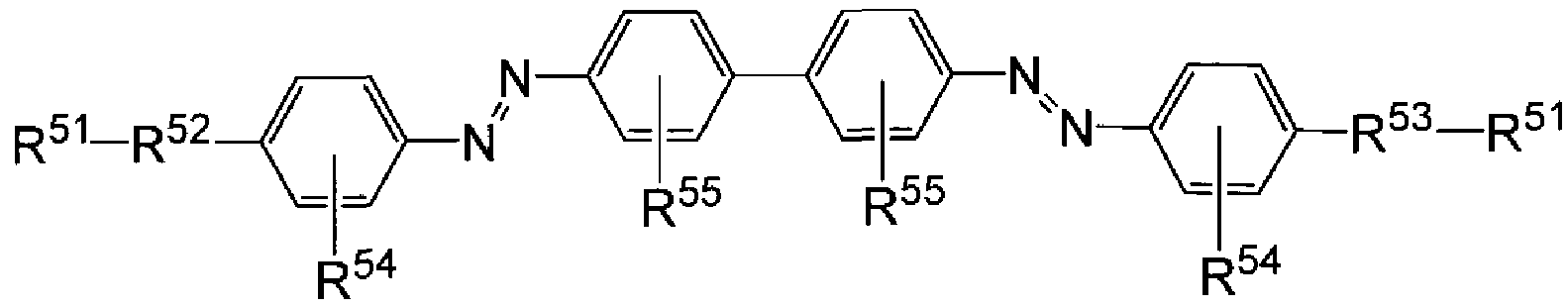
[0154] 上記式中、 R51は各々独立して、(メタ)アタリロイルォキシ基、(メタ)アクリルアミド基 、ビュルォキシ基、ビュルォキシカルボニル基、ビュルィミノカルボ-ル基、ビニルイミ
ノカルボ-ルォキシ基、ビュル基、イソプロぺ-ルォキシ基、イソプロべ-ルォキシカ ルボニル基、イソプロべ-ルイミノカルボ-ル基、イソプロべ-ルイミノカルボ-ルォキ シ基、イソプロぺニル基またはエポキシ基を表す。 R52は—(A51 B51— A51) - (D5 —で表される連結基を表し、 R53は (D51) — (A51— B51— A51) —で表される連結 n n m [0154] In the above formula, each R 51 independently represents a (meth) attaroyloxy group, a (meth) acrylamide group, a buroxy group, a buroxy carbonyl group, a burino mino carbo ol group, a vinyl imi It represents a no-carboxoxy group, a bur group, an isopropoxy group, an iso-propoxy carbonyl group, an iso-probe rimino carbo- caryl group, an iso-pro- leumino carboxy-oxy group, an isopropenyl group or an epoxy group. R 52 represents a linking group represented by — (A 51 B 51 — A 51 ) − (D 5 —, and R 53 represents (D 51 ) — (A 51 — B 51 — A 51 ) —. Concatenated nnm
基を表す。ここで、 A51は二価の炭化水素基を表し、 B51は— O—、— COO—、 -OC O 、 一CONH 、 一 NHCO 、 一 NHCOO または一OCONH を表し、 mは 0〜3の整数を表す。 D51は、 mが 0のとき二価の炭化水素基を表し、 mが 1〜3の整 数のとき一 O 、 一 COO 、 一 OCO 、 一 CONH 、 一 NHCO 、 一 NHCOO または OCONH を表し、 nは 0または 1を表す。 R54は各々独立して、ハロゲン 原子、カルボキシ基、ハロゲン化メチル基、ハロゲン化メトキシ基、シァノ基、ニトロ基 、メトキシ基またはメトキシカルボ-ル基を表す。ただし、カルボキシ基はアルカリ金属 と塩を形成していてもよい。 R55は各々独立して、カルボキシ基、スルホ基、ニトロ基、 アミノ基またはヒドロキシ基を表す。ただし、カルボキシ基またはスルホ基はアルカリ金 属と塩を形成して 、てもよ 、。 Represents a group. Here, A 51 represents a divalent hydrocarbon group, B 51 represents —O—, —COO—, —OC 2 O, 1 CONH, 1 NHCO, 1 NHCOO or 1 OCONH, and m is 0 to 3 Represents an integer. D 51 represents a divalent hydrocarbon group when m is 0, and represents one O, one COO, one OCO, one CONH, one NHCO, one NHCOO or OCONH when m is an integer of 1 to 3, n represents 0 or 1. R 54 each independently represents a halogen atom, a carboxy group, a halogenated methyl group, a halogenated methoxy group, a cyano group, a nitro group, a methoxy group or a methoxycarbon group. However, the carboxy group may form a salt with an alkali metal. Each R 55 independently represents a carboxy group, a sulfo group, a nitro group, an amino group or a hydroxy group. However, a carboxy group or a sulfo group may form a salt with an alkali metal.
[0155] 上記式で表される化合物の具体例としては、下記の化合物を挙げることができる。 [0155] Specific examples of the compound represented by the above formula include the following compounds.
[0156] [化 17]
[0156] [Chemical 17]
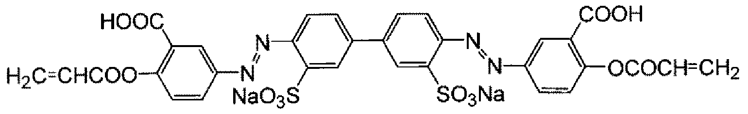

[0157] 本実施態様においては、このような光異性ィ匕反応性ィ匕合物の中から、要求特性に 応じて、シス—トランス異性ィ匕反応性骨格や置換基を種々選択することができる。な お、これらの光異性化反応性化合物は、 1種単独でも 2種以上を組み合わせて用い ることちでさる。 In this embodiment, a cis-trans isomerism reactive skeleton and substituents can be variously selected from such photoisomerism reactivity compounds according to required characteristics. it can. These photoisomerization-reactive compounds can be used singly or in combination of two or more.
[0158] 本実施態様に用いられる光異性ィ匕型の材料としては、上記光異性化反応性化合 物のほか、光配向膜の光配列性を妨げない範囲内で添加剤を含んでいてもよい。上 記光異性ィ匕反応性ィ匕合物として重合性モノマーを用いる場合には、添加剤としては 、重合開始剤、重合禁止剤などが挙げられる。 [0158] In addition to the photoisomerization reactive compound, the photoisomerization type material used in this embodiment may contain an additive within a range that does not interfere with the photoalignment property of the photoalignment film. Good. In the case where a polymerizable monomer is used as the photoisomerism-reactive compound, examples of the additive include a polymerization initiator and a polymerization inhibitor.
[0159] 重合開始剤または重合禁止剤は、一般に公知の化合物の中から、光異性化反応 性ィ匕合物の種類によって適宜選択して用いればょ ヽ。重合開始剤または重合禁止 剤の添加量は、光異性化反応性化合物に対し、 0. 001質量%〜20質量%の範囲 内であることが好ましぐ 0. 1質量%〜5質量%の範囲内であることがより好ましい。
重合開始剤または重合禁止剤の添加量が小さすぎると重合が開始 (禁止)されない 場合があり、逆に大きすぎると、反応が阻害される場合があるからである。 [0159] The polymerization initiator or polymerization inhibitor may be appropriately selected from generally known compounds according to the type of the photoisomerization-reactive compound. The addition amount of the polymerization initiator or the polymerization inhibitor is preferably in the range of 0.001% by mass to 20% by mass with respect to the photoisomerization reactive compound. More preferably within the range. This is because if the addition amount of the polymerization initiator or polymerization inhibitor is too small, the polymerization may not be started (prohibited), whereas if too large, the reaction may be inhibited.
[0160] (5)反応性配向層 [0160] (5) Reactive alignment layer
上記スぺーサー側基板の第 1配向膜上には反応性配向層が形成されていても良 い。スぺーサー側基板に用いられる反応性配向層については、上記「1.反応性配 向層」の項に記載したものと同様であるため、ここでの説明は省略する。 A reactive alignment layer may be formed on the first alignment film of the spacer side substrate. The reactive alignment layer used for the spacer-side substrate is the same as that described in the section “1. Reactive alignment layer” above, and thus the description thereof is omitted here.
[0161] 3.対向基板 [0161] 3. Counter substrate
次に、本実施態様に用いられる対向基板について説明する。本実施態様における 対向基板は、第 2基板と、上記第 2基板上に形成された第 2電極と、上記第 2電極上 に形成された第 2配向膜とを有するものである。また、第 2配向膜上には反応性配向 層が形成されていても良い。 Next, the counter substrate used in this embodiment will be described. The counter substrate in this embodiment has a second substrate, a second electrode formed on the second substrate, and a second alignment film formed on the second electrode. A reactive alignment layer may be formed on the second alignment film.
ここで、上記対向基板に用いられる第 2基板、第 2電極、および第 2配向膜は、上記 「2.スぺーサー側基板」の項に記載した第 1基板、第 1電極および第 1配向膜と同様 であるため、ここでの説明は省略する。また、対向基板に用いられる反応性配向層に ついては、上記「1.反応性配向層」の項に記載したものと同様であるため、ここでの 説明は省略する。 Here, the second substrate, the second electrode, and the second alignment film used for the counter substrate are the first substrate, the first electrode, and the first alignment described in the section “2. Spacer side substrate”. Since it is the same as the film, the explanation here is omitted. In addition, the reactive alignment layer used for the counter substrate is the same as that described in the section “1. Reactive alignment layer”, and thus the description thereof is omitted here.
[0162] 4.液晶層 [0162] 4. Liquid crystal layer
本実施態様の液晶表示素子が有する液晶層は液晶物質力 なるものである。液晶 層を構成する液晶物質は特に限定されるものではなぐ一般に液晶表示素子に用い られる液晶物質を用いることができる。 The liquid crystal layer included in the liquid crystal display element of this embodiment has liquid crystal substance power. The liquid crystal substance constituting the liquid crystal layer is not particularly limited, and a liquid crystal substance generally used for a liquid crystal display element can be used.
[0163] 上記液晶層の厚みは、 1 μ πι〜20 /ζ mの範囲内であるのが好ましぐより好ましくは 1 πι〜10 /ζ πι、さらに好ましくは 1. 2 /ζ πι〜5 /ζ πιの範囲内である。液晶層の厚み が薄すぎるとコントラストが低下するおそれがあり、逆に液晶層の厚みが厚すぎると液 晶物質が配向しに《なる可能性があるからである。 [0163] The liquid crystal layer preferably has a thickness in the range of 1 μπι to 20 / ζ m, more preferably 1 πι to 10 / ζ πι, and even more preferably 1.2 / ζ πι to 5 Within the range of / ζ πι. This is because if the thickness of the liquid crystal layer is too thin, the contrast may be lowered. Conversely, if the thickness of the liquid crystal layer is too thick, the liquid crystal substance may be oriented.
[0164] 5.その他 [0164] 5. Other
本実施態様における液晶表示素子は上記スぺーサー側基板、対向基板および液 晶層以外に他の構成を有していてもよい。このような他の構成としては、偏光板とシ ール剤とを挙げることができる。
[0165] 本実施態様においては、上記スぺーサー側基板と上記対向基板との間に、シール 剤を有することが好ましい。上記シール剤を有することにより、上記液晶層から液晶 物質が漏洩することを防止できるからである。本実施態様に用いられるシール剤の構 成材料としては、一般に液晶表示素子のシール剤に用いられるものを使用すること ができる。このような材料としては、例えば榭脂が挙げられ、熱硬化性榭脂および紫 外線硬化性榭脂の 、ずれも用いることができる。なかでも本実施態様にぉ 、ては、 上記シール剤が紫外線硬化性榭脂からなることが好ま ヽ。上記シール剤が紫外線 硬化性榭脂からなることにより、例えば、上記反応性配向層を構成する硬化性榭脂と して紫外線硬化性榭脂を用いた場合に、シール剤と反応性配向層とを同時に硬化 処理することが可能になるため、本実施態様の液晶表示素子の製造方法を簡略ィ匕 することができるカゝらである。本実施態様に用いられるシール剤としては、例えば、 U V硬化シール剤(商品名 LCB610 :EHC社製)を挙げることができる。 The liquid crystal display element in this embodiment may have other configurations in addition to the spacer side substrate, the counter substrate, and the liquid crystal layer. Examples of such other configurations include a polarizing plate and a sealant. [0165] In the present embodiment, it is preferable to have a sealing agent between the spacer-side substrate and the counter substrate. This is because the liquid crystal substance can be prevented from leaking from the liquid crystal layer by having the sealing agent. As a constituent material of the sealant used in this embodiment, those generally used for a sealant of a liquid crystal display element can be used. As such a material, for example, rosin can be used, and a shift between thermosetting rosin and ultraviolet curable rosin can also be used. In particular, in this embodiment, it is preferable that the sealing agent is made of an ultraviolet curable resin. When the sealing agent comprises an ultraviolet curable resin, for example, when an ultraviolet curable resin is used as the curable resin constituting the reactive alignment layer, the sealing agent and the reactive alignment layer Can be simultaneously cured, so that the manufacturing method of the liquid crystal display element of this embodiment can be simplified. Examples of the sealant used in this embodiment include a UV curable sealant (trade name LCB610: manufactured by EHC).
[0166] 本実施態様に用いられる偏光板は、光の波動のうち特定方向のみを透過させるも のであれば特に限定されるものではなぐ一般に液晶表示素子の偏光板として用い られて 、るものを使用することができる。 [0166] The polarizing plate used in the present embodiment is not particularly limited as long as it transmits only a specific direction of the wave of light, and is generally used as a polarizing plate of a liquid crystal display element. Can be used.
[0167] 本実施態様の液晶表示装置の駆動方法は、薄膜トランジスタ (TFT)を用いたァク ティブマトリックス方式であることが好まし 、。 TFT素子を用いたアクティブマトリックス 方式を採用することにより、目的の画素を確実に点灯、消灯できるため高品質なディ スプレイが可能となる力もである。 [0167] The driving method of the liquid crystal display device of the present embodiment is preferably an active matrix method using a thin film transistor (TFT). By adopting an active matrix method using TFT elements, the target pixel can be reliably turned on and off, which enables high-quality display.
[0168] 本実施態様の TFTを用いたアクティブマトリックス方式の液晶表示素子の一例を示 す概略斜視図を図 4に示す。図 4に例示する液晶表示素子 20は、一方の基板 22a 上に TFT25がマトリックス状に配置された TFT基板 21aと、他方の基板 22b上に共 通電極 23が形成された共通電極基板 21bとを有するものである。 TFT基板 21aには 、 X電極 24x、 y電極 24yおよび画素電極 24tが形成されている。このような液晶表示 素子 20において、 X電極 24xおよび y電極 24yはそれぞれ縦横に配列しており、これ らの電極 24xおよび 24yに信号をカ卩えることにより TFT素子 25を作動させ、液晶物 質を駆動させることができる。 X電極 24xおよび y電極 24yが交差した部分は、図示し ないが絶縁層で絶縁されており、 X電極 24xの信号と y電極 24yの信号とは独立に動
作することができる。 X電極 24xおよび y電極 24yにより囲まれた部分は、本実施態様 の液晶表示素子を駆動する最小単位である画素であり、各画素には少なくとも 1っ以 上の TFT素子 25および画素電極 24tが形成されて!、る。この液晶表示素子 20では 、 X電極 24xおよび y電極 24yに順次信号電圧を加えることにより、各画素の TFT素 子 25を動作させることができる。 FIG. 4 is a schematic perspective view showing an example of an active matrix type liquid crystal display element using TFTs of the present embodiment. The liquid crystal display element 20 illustrated in FIG. 4 includes a TFT substrate 21a in which TFTs 25 are arranged in a matrix on one substrate 22a, and a common electrode substrate 21b in which a common electrode 23 is formed on the other substrate 22b. It is what you have. An X electrode 24x, a y electrode 24y, and a pixel electrode 24t are formed on the TFT substrate 21a. In such a liquid crystal display element 20, the X electrode 24x and the y electrode 24y are arranged vertically and horizontally, respectively, and the TFT element 25 is activated by capturing a signal on these electrodes 24x and 24y, and the liquid crystal material Can be driven. The portion where X electrode 24x and y electrode 24y intersect is insulated by an insulating layer (not shown), and the signal of X electrode 24x and the signal of y electrode 24y move independently. Can be made. The portion surrounded by the X electrode 24x and the y electrode 24y is a pixel that is the minimum unit for driving the liquid crystal display element of this embodiment, and each pixel has at least one TFT element 25 and pixel electrode 24t. Formed! In the liquid crystal display element 20, the TFT element 25 of each pixel can be operated by sequentially applying a signal voltage to the X electrode 24x and the y electrode 24y.
なお、図 4において、液晶層および配向膜は省略している。 In FIG. 4, the liquid crystal layer and the alignment film are omitted.
[0169] 本実施態様の液晶表示素子を上記 TFT素子を用いたアクティブマトリックス方式に より駆動する場合においては、上記スぺーサー側基板を上記 TFT基板とし、上記対 向基板を上記共通電極基板としても良ぐまた上記対向基板を上記 TFT基板とし、 上記スぺーサー側基板を上記共通電極基板としても良い。 [0169] When the liquid crystal display element of this embodiment is driven by the active matrix method using the TFT element, the spacer-side substrate is the TFT substrate, and the counter substrate is the common electrode substrate. The counter substrate may be the TFT substrate, and the spacer substrate may be the common electrode substrate.
[0170] 次に、本実施態様の液晶表示素子の用途について説明する。本実施態様の液晶 表示素子は、上記薄膜トランジスタ (TFT)を用いたアクティブマトリックス方式により 駆動させ、カラーフィルタ方式またはフィールドシーケンシャルカラー方式を採用する ことによりカラーの液晶表示素子として用いることができる。 Next, the use of the liquid crystal display element of this embodiment will be described. The liquid crystal display element of this embodiment can be used as a color liquid crystal display element by being driven by an active matrix method using the thin film transistor (TFT) and employing a color filter method or a field sequential color method.
[0171] 本実施態様の液晶表示素子の製造方法は、上述した内容の各構成を製造できる 方法であれば、特に限定されないが、例えば、「A— 2.液晶表示素子の製造方法」 の項において説明する製造方法により製造することができる。 [0171] The method for producing a liquid crystal display element of the present embodiment is not particularly limited as long as it is a method capable of producing each of the components described above. For example, the section "A-2. Method for producing liquid crystal display element" It can manufacture with the manufacturing method demonstrated in (1).
[0172] A— 2.液晶表示素子の製造方法 [0172] A— 2. Method of manufacturing liquid crystal display element
次に、本発明の第 1実施態様の液晶表示素子の製造方法について説明する。本 実施態様の液晶表示素子の製造方法は、第 1基板と、上記第 1基板上に形成された 第 1電極と、上記第 1電極上に形成されたスぺーサ一と、上記第 1電極および上記ス ぺーサ一上に形成された第 1配向膜とを有するスぺーサー側基板、および、第 2基 板と、上記第 2基板上に形成された第 2電極と、上記第 2電極上に形成された第 2配 向膜とを有する対向基板を用いる液晶表示素子の製造方法である。 Next, a method for manufacturing the liquid crystal display element of the first embodiment of the present invention will be described. The method of manufacturing a liquid crystal display element according to this embodiment includes a first substrate, a first electrode formed on the first substrate, a spacer formed on the first electrode, and the first electrode. And a spacer side substrate having a first alignment film formed on the spacer, a second substrate, a second electrode formed on the second substrate, and the second electrode. This is a method for manufacturing a liquid crystal display element using a counter substrate having a second alignment film formed thereon.
[0173] 本実施態様の液晶表示素子の製造方法は、液晶層の形成方法により 2態様に大 別することができる。以下、各態様に分けて本実施態様の液晶表示素子の製造方法 について説明する。 [0173] The method for producing a liquid crystal display element of the present embodiment can be roughly divided into two embodiments depending on the method for forming the liquid crystal layer. Hereinafter, the manufacturing method of the liquid crystal display element of this embodiment will be described separately for each embodiment.
[0174] A— 2— 1.第 1態様
まず、本実施態様の液晶表示素子の製造方法の第 1態様について説明する。本態 様の液晶表示素子の製造方法は、第 1基板と、上記第 1基板上に形成された第 1電 極と、上記第 1電極上に形成されたスぺーサ一と、上記第 1電極および上記スぺーサ 一上に形成された第 1配向膜とを有するスぺーサー側基板、および、第 2基板と、上 記第 2基板上に形成された第 2電極と、上記第 2電極上に形成された第 2配向膜とを 有する対向基板を用いる液晶表示素子の製造方法であって、上記第 1配向膜上また は上記第 2配向膜上の少なくとも一方に未硬化の硬化性榭脂を含む未硬化反応性 配向層を形成する未硬化反応性配向層形成工程と、上記未硬化反応性配向層を介 して上記第 1配向膜と上記第 2配向膜とが向かい合うように上記スぺーサー側基板と 上記対向基板とを接触させた後、上記硬化性榭脂を硬化することにより、上記スぺー サー側基板と上記対向基板とを接着させて液晶表示素子用基板対を形成する液晶 表示素子用基板対形成工程と、上記液晶表示素子用基板対形成工程により形成さ れた液晶表示素子用基板対のスぺーサー側基板と対向基板との間に、液晶層を形 成する液晶層形成工程と、カゝらなることを特徴とするものである。 [0174] A— 2— 1. First aspect First, a first aspect of the method for manufacturing a liquid crystal display element of this embodiment will be described. A liquid crystal display device manufacturing method according to this aspect includes a first substrate, a first electrode formed on the first substrate, a spacer formed on the first electrode, and the first electrode. And a spacer side substrate having a first alignment film formed on the spacer, a second substrate, a second electrode formed on the second substrate, and the second electrode. A method of manufacturing a liquid crystal display device using a counter substrate having a second alignment film formed thereon, wherein at least one of the first alignment film and the second alignment film is uncured curable resin. An uncured reactive alignment layer forming step for forming an uncured reactive alignment layer containing fat, and the first alignment film and the second alignment film facing each other through the uncured reactive alignment layer. After contacting the spacer side substrate and the counter substrate, by curing the curable resin, the above A liquid crystal display element substrate pair forming step of bonding a spacer side substrate and the counter substrate to form a liquid crystal display element substrate pair, and a liquid crystal display element substrate pair forming step. A liquid crystal layer forming step for forming a liquid crystal layer between the spacer side substrate of the pair of substrates and the counter substrate is characterized by the fact that the liquid crystal layer is formed.
本態様の液晶表示素子の製造方法について、図を参照しながら説明する。図 5は 本態様に係る液晶表示素子の製造方法の一例を工程図である。図 5に示すように本 態様の製造方法は、まず、第 1基板 laと、上記第 1基板 la上に形成された第 1電極 2 aと、上記第 1電極 2a上に形成されたスぺーサー 4と、上記第 1電極 2aおよび上記ス ぺーサ一 4上に形成された第 1配向膜 3aとを有するスぺーサー側基板 11、および、 第 2基板 2aと、上記第 2基板 2a上に形成された第 2電極 2bと、上記第 2電極 2b上に 形成された第 2配向膜 3bとを有する対向基板 12を用意する(図 5 (a) )。 The manufacturing method of the liquid crystal display element of this aspect is demonstrated referring a figure. FIG. 5 is a process diagram illustrating an example of a method for manufacturing a liquid crystal display element according to this embodiment. As shown in FIG. 5, in the manufacturing method of this embodiment, first, the first substrate la, the first electrode 2a formed on the first substrate la, and the spacer formed on the first electrode 2a. A spacer-side substrate 11 having a substrate 4 and a first alignment film 3a formed on the first electrode 2a and the spacer 4; a second substrate 2a; and the second substrate 2a. A counter substrate 12 having a second electrode 2b formed on the second electrode 2b and a second alignment film 3b formed on the second electrode 2b is prepared (FIG. 5A).
次に、上記スぺーサー側基板 11の上記第 1配向膜 3a上に未硬化の硬化性榭脂か らなる未硬化反応性配向^を形成する (未硬化反応性配向層形成工程:図 5 (b) )。 次に、上記スぺーサー側基板 11の第 1配向膜 3a上に形成された上記未硬化反応 性配向層^と、上記対向基板 12の上記第 2配向膜 3bとを向かい合うように接触させ た後、上記未硬化反応性配向層 5Ίこ含まれる未硬化の硬化性榭脂を硬化し、反応 性配向層 5とすることにより、上記スぺーサー側基板 11と上記対向基板 12とを接着さ せて液晶表示素子用基板対 40を形成する (液晶表示素子用基板対形成工程:図 5 (
c) ) 0また、上記未硬化の硬化性榭脂を硬化して反応性配向層 5を形成する際に、未 硬化の硬化性榭脂からなるシール剤を同時に硬化させて、上記スぺーサー側基板 1 1と上記対向基板 12との間をシール剤 7を形成しても良い。 Next, an uncured reactive alignment layer made of an uncured curable resin is formed on the first alignment film 3a of the spacer-side substrate 11 (uncured reactive alignment layer forming step: FIG. (b)). Next, the uncured reactive alignment layer ^ formed on the first alignment film 3a of the spacer-side substrate 11 and the second alignment film 3b of the counter substrate 12 were brought into contact with each other so as to face each other. Thereafter, the uncured curable resin contained in the uncured reactive alignment layer 5 is cured to form the reactive alignment layer 5 so that the spacer-side substrate 11 and the counter substrate 12 are bonded. To form a liquid crystal display element substrate pair 40 (liquid crystal display element substrate pair formation process: FIG. c)) 0 Further , when the uncured curable resin is cured to form the reactive alignment layer 5, a sealant made of the uncured curable resin is simultaneously cured to form the spacer. A sealant 7 may be formed between the side substrate 11 and the counter substrate 12.
次に、上記液晶表示素子用基板対 40のスぺーサー側基板 11と対向基板 12との 間に、液晶物質を注入することにより液晶層 6を形成する (液晶層形成工程:図 5 (d) )。本態様は、以上の工程により液晶表示素子を製造するものである。 Next, a liquid crystal layer 6 is formed by injecting a liquid crystal material between the spacer-side substrate 11 and the counter substrate 12 of the liquid crystal display element substrate pair 40 (liquid crystal layer forming step: FIG. )). In this embodiment, a liquid crystal display element is manufactured by the above process.
[0176] 本態様によれば、上記スぺーサー側基板と上記対向基板とを反応性配向層を介し て強固に固定することができるため、セルギャップの変動のない表示品質に優れた 液晶表示素子を製造することができる。 [0176] According to this aspect, since the spacer-side substrate and the counter substrate can be firmly fixed via the reactive alignment layer, a liquid crystal display excellent in display quality with no cell gap variation An element can be manufactured.
以下、本態様の液晶表示素子の製造方法について詳細に説明する。 Hereafter, the manufacturing method of the liquid crystal display element of this aspect is demonstrated in detail.
[0177] 1.未硬化反応性配向層形成工程 [0177] 1. Uncured reactive alignment layer formation process
まず、本態様における未硬化反応性配向層形成工程について説明する。本態様 における未硬化反応性配向層形成工程は、上記スぺーサー側基板の第 1配向膜上 または上記対向基板の第 2配向膜上の少なくとも一方に、未硬化の硬化性榭脂から なる未硬化反応性配向層を形成する工程である。 First, the uncured reactive alignment layer forming step in this embodiment will be described. In the present embodiment, the uncured reactive alignment layer forming step includes an uncured curable resin formed on at least one of the first alignment film on the spacer-side substrate and the second alignment film on the counter substrate. This is a step of forming a curing reactive alignment layer.
なお、本工程により形成される未硬化反応性配向層は、後述する液晶表示素子用 基板対形成工程において上記未硬化の硬化性榭脂が硬化されることにより、反応性 配向層となるものである。 The uncured reactive alignment layer formed in this step becomes a reactive alignment layer by curing the above-mentioned uncured curable resin in the substrate pair forming step for liquid crystal display elements described later. is there.
以下、本態様における未硬化反応性配向層形成工程について説明する。 Hereinafter, the uncured reactive alignment layer forming step in this embodiment will be described.
[0178] (1)スぺーサー側基板形成工程 [0178] (1) Spacer side substrate formation process
本態様にお!ヽて用いるスぺーサー側基板を形成するスぺーサー側基板形成工程 について説明する。スぺーサー側基板形成工程は、第 1基板と、上記第 1基板上に 形成された第 1電極と、上記第 1電極上に形成されたスぺーサ一と、上記第 1電極お よび上記スぺーサー上に形成された第 1配向膜とを有するスぺーサー側基板を形成 する工程である。通常このようなスぺーサー側基板形成工程は、第 1基板上に第 1電 極を形成する第 1電極形成工程と、上記第 1電極形成工程により形成された第 1電極 上にスぺーサーを形成するスぺーサ一形成工程と、上記スぺーサ一形成工程の後、 第 1電極上とスぺーサー上に第 1配向膜を形成する第 1配向膜形成工程とからなる。
[0179] i)第 1電極形成工程 A spacer-side substrate forming step for forming a spacer-side substrate used in this embodiment will be described. The spacer side substrate forming step includes a first substrate, a first electrode formed on the first substrate, a spacer formed on the first electrode, the first electrode, and the first electrode. This is a step of forming a spacer side substrate having a first alignment film formed on the spacer. In general, the spacer-side substrate forming process includes a first electrode forming process for forming the first electrode on the first substrate and a spacer on the first electrode formed by the first electrode forming process. And a first alignment film forming step for forming a first alignment film on the first electrode and the spacer after the spacer formation step. [0179] i) First electrode formation step
まず、第 1電極形成工程について説明する。第 1電極形成工程は第 1基板上に第 1 電極層を形成する工程である。 First, the first electrode forming process will be described. The first electrode forming step is a step of forming the first electrode layer on the first substrate.
[0180] 本工程において上記第 1基板上に第 1電極を形成する方法としては、厚みが均一 な第 1電極を形成できる方法であれば特に限定されるものではな 、。このような第 1電 極の形成方法としては、例えば化学蒸着 (CVD)法や、スパッタリング法、イオンプレ 一ティング法、真空蒸着法等の物理蒸着 (PVD)法などを挙げることができる。また、 電極層のパター-ング方法としては、一般的な電極のパター-ング方法を適用する ことができる。 [0180] The method for forming the first electrode on the first substrate in this step is not particularly limited as long as the first electrode can be formed with a uniform thickness. Examples of the method for forming the first electrode include chemical vapor deposition (CVD), physical vapor deposition (PVD) such as sputtering, ion plating, and vacuum deposition. Further, as a patterning method for the electrode layer, a general electrode patterning method can be applied.
[0181] なお、本工程に用いられる第 1基板および第 1電極のその他の点については、上記 「A— 1.液晶表示素子 2.スぺーサー側基板」の項に記載したものと同様であるた め、ここでの説明は省略する。 [0181] The other points of the first substrate and the first electrode used in this step are the same as those described in the above section “A-1. Liquid crystal display element 2. Spacer side substrate”. Therefore, the explanation here is omitted.
[0182] ii)スぺーサ一形成工程 [0182] ii) Spacer formation process
次に、スぺーサ一形成工程について説明する。スぺーサ一形成工程は上記第 1電 極形成工程より形成された第 1電極上にスぺーサーを形成する工程である。 Next, the spacer forming process will be described. The spacer forming step is a step of forming a spacer on the first electrode formed in the first electrode forming step.
[0183] 第 1電極上へのスぺーサ一の形成方法としては、所定の位置に所望の形状のスぺ 一サーを精度良く形成することが可能な方法であれば特に限定されるものではなぐ 一般的なパターユング法を適用することができる。このようなパターユング法としては 、 2P (Photo Polymerization)法、フォトリソグラフィ一法、インクジェット法、スクリ ーン印刷法等の公知の方法により形成することができる。 2P法では、例えば、ェチレ ングリコール(メタ)アタリレート、ジエチレングリコールジ(メタ)アタリレート、プロピレン グリコールジ (メタ)アタリレート、ジプロピレングリコールジ (メタ)アタリレート、ポリェチ レングリコールジ(メタ)アタリレート、ポリプロピレングリコールジ (メタ)アタリレート、へ キサングリコールジ (メタ)アタリレート、ネオペンチルグリコールジ (メタ)アタリレート、 グリセリンジ (メタ)アタリレート、グリセリントリジ (メタ)アタリレート、トリメチロールプロパ ンジ (メタ)アタリレート、 1, 4 ブタンジオールジアタリレート、ペンタエリスリトール (メ タ)アタリレート、ジペンタエリスリトールトリ(メタ)アタリレート、ペンタエリスリトールテト ラ(メタ)アタリレート、ジペンタエリスリトールへキサ (メタ)アタリレート、ジペンタエリスリ
トールペンタ (メタ)アタリレート等の紫外線硬化性モノマーや、ウレタンアタリレート、 エポキシアタリレート、ポリエステルアタリレート、エポキシ、ビュルエーテル、ポリエン' チオール系等のオリゴマー、光二量ィ匕反応を起こすポリビニル桂皮酸系榭脂等の光 架橋型ポリマー等の榭脂組成物を基材上に塗布し、スぺーサ一形成用の原版を塗 布膜に圧着した状態で紫外線を照射して硬化させ、その後、原版を剥離することによ りスぺーサーを形成する。また、フォトリソグラフィ一法では、上述の 2P法で例示した ような材料を基材上に塗布し、スぺーサ一形成用の所望のフォトマスクを介して塗布 膜を露光し、その後、現像することによりスぺーサーを形成する。なお、上記の (メタ) アタリレートとは、アタリレートある 、はメタタリレートを意味する。 [0183] The method for forming the spacer on the first electrode is not particularly limited as long as it is a method capable of accurately forming a spacer having a desired shape at a predetermined position. Nagu General patterning method can be applied. Such a patterning method can be formed by a known method such as a 2P (Photo Polymerization) method, a photolithography method, an inkjet method, or a screen printing method. In the 2P method, for example, ethylene glycol (meth) acrylate, diethylene glycol di (meth) acrylate, propylene glycol di (meth) acrylate, dipropylene glycol di (meth) acrylate, polyethylene glycol di (meth) acrylate Polypropylene glycol di (meth) acrylate, hexane glycol di (meth) acrylate, neopentyl glycol di (meth) acrylate, glycerol di (meth) acrylate, glycerol tridi (meth) acrylate, trimethylolproparate 1,4-butanediol diatalylate, pentaerythritol (meth) acrylate, dipentaerythritol tri (meth) acrylate, pentaerythritol tetra (meth) acrylate, dipe Ntaerythritol hexa (meth) atalylate, dipentaerythri UV curable monomers such as tall penta (meth) acrylate, urethane acrylate, epoxy acrylate, polyester acrylate, epoxy, butyl ether, polyene thiol-based oligomers, polyvinyl cinnamate that causes photodimerization reaction A resin composition such as a photocrosslinkable polymer such as a resin-based resin is coated on a substrate, and the original for forming the spacer is cured by being irradiated with ultraviolet rays in a state where it is pressed against the coating film. A spacer is formed by peeling the original plate. In the photolithography method, a material as exemplified in the above-mentioned 2P method is applied onto a substrate, the coated film is exposed through a desired photomask for forming a spacer, and then developed. To form a spacer. Note that the above (meta) atelate means talate, and means metatalate.
[0184] なお、スぺーサ一のその他の点については、上記「A— 1.液晶表示素子 2.スぺ 一サー側基板」の項に記載したものと同様であるため、ここでの説明は省略する。 [0184] The other points of the spacer are the same as those described in the above section "A- 1. Liquid crystal display element 2. Spacer side substrate". Is omitted.
[0185] iii)第 1配向膜形成工程 [0185] iii) First alignment film forming step
次に、第 1配向膜形成工程について説明する。第 1配向膜形成工程は上記第 1電 極形成工程およびスぺーサ一形成工程により形成された、第 1電極およびスぺーサ 一上に第 1配向膜を形成する工程である。第 1配向膜形成工程においては、ラビング 配向膜を形成してもよぐ光配向膜を形成してもよい。 Next, the first alignment film forming step will be described. The first alignment film forming step is a step of forming the first alignment film on the first electrode and the spacer formed by the first electrode forming step and the spacer forming step. In the first alignment film forming step, a rubbing alignment film or a photo-alignment film may be formed.
[0186] a.光配向膜の形成方法 [0186] a. Method of forming photo-alignment film
第 1配向膜形成工程において光配向膜を形成するには、まず光配向膜の構成材 料を有機溶剤で希釈した光配向膜形成用塗工液を電極層上に塗布し、乾燥させる。 この場合に、光配向膜形成用塗工液中の光二量ィ匕反応性ィ匕合物または光異性ィ匕 反応性化合物の含有量は、 0. 05質量%〜 10質量%の範囲内であることが好ましく 、 0. 2質量%〜2質量%の範囲内であることがより好ましい。含有量が上記範囲より 少ないと、第 1配向膜に適度な異方性を付与することが困難となり、逆に含有量が上 記範囲より多いと、光配向膜形成用塗工液の粘度が高くなるので均一な塗膜を形成 しにくくなる力 である。 In order to form the photo-alignment film in the first alignment film forming step, first, a photo-alignment film-forming coating solution obtained by diluting the constituent material of the photo-alignment film with an organic solvent is applied on the electrode layer and dried. In this case, the content of the photodimer-reactive compound or photoisomerism-reactive compound in the coating liquid for forming a photo-alignment film is within the range of 0.05% by mass to 10% by mass. It is preferable that it is within the range of 0.2% by mass to 2% by mass. If the content is less than the above range, it will be difficult to impart appropriate anisotropy to the first alignment film. Conversely, if the content is more than the above range, the viscosity of the photoalignment film-forming coating solution will be low. Since it becomes higher, it is a force that makes it difficult to form a uniform coating film.
[0187] 光配向膜形成用塗工液の塗布方法としては、例えばスピンコート法、ロールコート 法、ロッドバーコート法、スプレーコート法、エアナイフコート法、スロットダイコート法、 ワイヤーバーコート法などを用いることができる。
[0188] 上記光配向膜形成用塗工液を塗布することにより得られる膜の厚みは、 Inn!〜 20 OOnmの範囲内であることが好ましく、より好ましくは 3nm〜 lOOnmの範囲内である。 膜の厚みが上記範囲より薄いと十分な光配列性を得ることができない可能性があり、 逆に厚みが上記範囲より厚いとコスト的に不利になる場合があるからである。 [0187] Examples of the application method of the coating liquid for forming a photo-alignment film include spin coating, roll coating, rod bar coating, spray coating, air knife coating, slot die coating, and wire bar coating. be able to. [0188] The thickness of the film obtained by applying the coating liquid for forming a photo-alignment film is Inn! It is preferably in the range of ˜20 OOnm, more preferably in the range of 3 nm to lOOnm. This is because if the thickness of the film is thinner than the above range, sufficient optical alignment may not be obtained, and conversely, if the thickness is thicker than the above range, it may be disadvantageous in terms of cost.
[0189] 得られた膜には光配向処理を施すことによって異方性を付与する。具体的には、得 られた膜に、偏光を制御した光を照射することにより、光励起反応を生じさせて異方 性を付与することができる。照射する光の波長領域は、第 1光配向膜の構成材料に 応じて適宜選択すればよいが、紫外光域の範囲内、すなわち 100nm〜400nmの 範囲内であることが好ましく、より好ましくは 250nm〜380nmの範囲内である。 [0189] Anisotropy is imparted to the obtained film by performing a photo-alignment treatment. Specifically, by irradiating the obtained film with light whose polarization is controlled, a photoexcitation reaction is caused and anisotropy can be imparted. The wavelength region of the light to be irradiated may be appropriately selected according to the constituent material of the first photo-alignment film, but is preferably in the ultraviolet light range, that is, in the range of 100 nm to 400 nm, more preferably 250 nm. Within the range of ~ 380 nm.
[0190] さらに、光配向膜の構成材料として、光異性化反応性化合物の中でも重合性モノ マーを用いた場合には、光配向処理を行った後、加熱することにより、ポリマー化し、 第 1配向膜に付与された異方性を安定ィ匕することができる。 [0190] Further, when a polymerizable monomer is used as a constituent material of the photo-alignment film among the photoisomerization-reactive compounds, the photo-alignment treatment is performed, and then the polymer is formed by heating. The anisotropy imparted to the alignment film can be stabilized.
[0191] b.ラビング膜の形成方法 [0191] b. Method of forming rubbing film
第 1配向膜形成工程においてラビング膜を形成する方法としては特に限定されるも のではなぐ一般に液晶表示素子用のラビング膜の形成方法を適用することができる The method for forming the rubbing film in the first alignment film forming step is not particularly limited, and generally a rubbing film forming method for a liquid crystal display element can be applied.
[0192] cその他 [0192] cOther
なお、第 1配向膜の構成材料およびその他の点については、上記「A—1.液晶表 示素子 2.スぺーサー側基板」の項に記載したものと同様であるため、ここでの説明 は省略する。 The constituent material and other points of the first alignment film are the same as those described in the above section “A-1. Liquid crystal display element 2. Spacer side substrate”, and therefore are described here. Is omitted.
[0193] (2)対向基板形成工程 [0193] (2) Opposing substrate formation process
次に、本態様の液晶表示素子の製造方法に用いる対向基板を形成する対向基板 形成工程について説明する。対向基板形成工程は、第 2基板と、上記第 2基板上に 形成された第 2電極と、上記第 2電極上に形成された第 2配向膜とを有する対向基板 を形成する工程である。通常このような対向基板形成工程は、第 2基板上に第 2電極 を形成する第 2電極形成工程と、上記第 2電極形成工程により形成された第 2電極上 に第 2配向膜を形成する第 2配向膜形成工程とからなる。 Next, a counter substrate forming process for forming a counter substrate used in the method for manufacturing a liquid crystal display element of this aspect will be described. The counter substrate forming step is a step of forming a counter substrate having a second substrate, a second electrode formed on the second substrate, and a second alignment film formed on the second electrode. Usually, in the counter substrate forming step, a second electrode is formed on the second substrate, and a second alignment film is formed on the second electrode formed by the second electrode forming step. A second alignment film forming step.
[0194] i)第 2電極形成工程
第 2電極形成工程は、第 2基板上に第 2電極を形成する工程である。第 2電極形成 工程における第 2電極の形成方法は、上述した「(1)スぺーサー側基板形成工程 0 第 1電極形成工程」の項に記載したものと同様であるため、ここでの説明は省略する I) Second electrode formation process The second electrode forming step is a step of forming the second electrode on the second substrate. The method of forming the second electrode in the second electrode forming step is the same as that described in the section “(1) Spacer side substrate forming step 0 First electrode forming step” described above. Is omitted
[0195] また、第 2電極形成工程に用いる第 2基板、第 2電極の構成材料および第 2電極に 関するその他の点については、上記「A— 1.液晶表示素子 3.対向基板」の項に 記載したものと同様であるため、ここでの説明は省略する。 [0195] Also, regarding the second substrate used in the second electrode formation step, the constituent material of the second electrode, and other points related to the second electrode, refer to the section “A-1. Since it is the same as that described in, the explanation here is omitted.
[0196] ii)第 2配向膜形成工程 [0196] ii) Second alignment film formation step
第 2配向膜形成工程は、上記第 2電極形成工程により形成された第 2電極上に第 2 配向膜を形成する工程である。第 2配向膜形成工程における第 2配向膜の形成方法 については、上記「(1)スぺーサー側基板形成工程 iii)第 1配向膜形成工程」の項 に記載したものと同様であるため、ここでの説明は省略する。 The second alignment film forming step is a step of forming the second alignment film on the second electrode formed by the second electrode forming step. The method for forming the second alignment film in the second alignment film forming step is the same as that described in the section “(1) Spacer side substrate forming step iii) First alignment film forming step”. The description here is omitted.
[0197] また、第 2配向膜の構成材料およびその他の点については、上記「A— 1.液晶表 示素子 3.対向基板」の項に記載したものと同様であるため、ここでの説明は省略す る。 [0197] In addition, the constituent material and other points of the second alignment film are the same as those described in the above section "A- 1. Liquid crystal display element 3. Counter substrate". Is omitted.
[0198] (3)未硬化反応性配向層の形成方法 [0198] (3) Method for forming uncured reactive alignment layer
次に本工程において、上記スぺーサー側基板の第 1配向膜上または上記対向基 板の第 2配向膜上の少なくとも一方に、未硬化の硬化性榭脂からなる未硬化反応性 配向層を形成する方法について説明する。 Next, in this step, an uncured reactive alignment layer composed of an uncured curable resin is provided on at least one of the first alignment film of the spacer-side substrate or the second alignment film of the counter substrate. A method of forming will be described.
[0199] 本工程において、未硬化反応性配向層を形成する方法としては、未硬化の硬化性 榭脂を含む反応性配向層形成用塗工液を塗布し、配向処理を行う方法と、未硬化の 硬化性榭脂を含むドライフィルム等を予め形成し、これを積層する方法とを挙げること ができるが、本態様においては、未硬化の硬化性榭脂を含む反応性配向層形成用 塗工液を塗布し、配向処理を行う方法が好ましい。このような方法によれば未硬化反 応性配向層工程を簡略ィ匕することが可能である利点を有するからである。 [0199] In this step, as a method of forming an uncured reactive alignment layer, a method of applying an alignment treatment by applying a coating solution for forming a reactive alignment layer containing an uncured curable resin, Examples of the method include forming a dry film containing a curable curable resin in advance and laminating the film. In this embodiment, the coating for forming a reactive alignment layer containing an uncured curable resin is used. A method of applying a working solution and performing an alignment treatment is preferable. This is because such a method has an advantage that the uncured reactive alignment layer process can be simplified.
[0200] 上記反応性配向層用塗工液に用いる溶媒としては、上記硬化性榭脂等を溶解す ることができ、かつ第 1配向膜または第 2配向膜の配向能を阻害しないものであれば 特に限定はされない。例えば、ベンゼン、トルエン、キシレン、 n—ブチルベンゼン、
ジェチルベンゼン、テトラリン等の炭化水素類;メトキシベンゼン、 1, 2—ジメトキシべ ンゼン、ジエチレングリコールジメチルエーテル等のエーテル類;アセトン、メチルェ チルケトン、メチルイソブチルケトン、シクロへキサノン、 2, 4 ペンタンジオン等のケ トン類;酢酸ェチル、プロピレングリコールモノメチルエーテルアセテート、プロピレン グリコールモノェチルエーテルアセテート、 y ブチロラタトン等のエステル類; 2—ピ 口リドン、 N—メチルー 2—ピロリドン、ジメチルホルムアミド、ジメチルァセトアミド等の アミド系溶媒; t—ブチルアルコール、ジアセトンアルコール、グリセリン、モノァセチン 、エチレングリコーノレ、トリエチレングリコール、へキシレングリコール等のアルコール 類;フエノール、パラクロロフエノール等のフエノール類;メチルセ口ソルブ、ェチルセ口 ソルブ、ブチルセ口ソルブ、エチレングリコールモノメチルエーテルアセテート等のセ 口ソルブ類等の 1種または 2種以上が使用可能である。 [0200] The solvent used in the coating solution for the reactive alignment layer is one that can dissolve the curable resin and does not inhibit the alignment ability of the first alignment film or the second alignment film. If there is no particular limitation. For example, benzene, toluene, xylene, n-butylbenzene, Hydrocarbons such as jetylbenzene and tetralin; ethers such as methoxybenzene, 1,2-dimethoxybenzene and diethylene glycol dimethyl ether; ketones such as acetone, methyl ethyl ketone, methyl isobutyl ketone, cyclohexanone and 2, 4 pentanedione Tones; Esters such as ethyl acetate, propylene glycol monomethyl ether acetate, propylene glycol monoethyl ether acetate, and butyrolatataton; Amides such as 2-pyridone, N-methyl-2-pyrrolidone, dimethylformamide, dimethylacetamide, etc. Solvents; alcohols such as t-butyl alcohol, diacetone alcohol, glycerin, monoacetin, ethylene glycol, triethylene glycol, hexylene glycol; phenol, parachlore One or two or more kinds of phenols such as lofenol; such as methyl mouth solve, ethyl acetate mouth sorb, butyl mouth mouth sorb, and ethylene glycol monomethyl ether acetate can be used.
[0201] また、単一種の溶媒を使用しただけでは、上記硬化性榭脂等の溶解性が不十分で あったり、上述したように第 1配向膜が侵食されたりする場合がある。しかしながら、 2 種以上の溶媒を混合使用することにより、この不都合を回避することができる。上記 の溶媒のなかにあって、単独溶媒として好ましいものは、炭化水素類とダリコールモノ エーテルアセテート系溶媒であり、混合溶媒として好ましいのは、エーテル類または ケトン類と、グリコール系溶媒との混合系である。 [0201] Further, the use of a single type of solvent may result in insufficient solubility of the curable resin or the first alignment film may be eroded as described above. However, this inconvenience can be avoided by using a mixture of two or more solvents. Among the above-mentioned solvents, hydrocarbons and darlicol monoether acetate solvents are preferable as single solvents, and mixed solvents are preferably a mixture of ethers or ketones and glycol solvents. It is a system.
[0202] 反応性配向層用塗工液の濃度は、硬化性榭脂の溶解性や、形成しょうとする反応 性配向層の厚みに依存するため一概には規定できないが、通常は 0. 1質量%〜40 質量%、好ましくは 1質量%〜20質量%の範囲で調整される。反応性配向層用塗工 液の濃度が上記範囲より低いと、例えば、上記硬化性榭脂として反応性液晶を用い た場合に、反応性液晶が配向しに《なる可能性があり、逆に反応性配向層用塗工 液の濃度が上記範囲より高いと、反応性配向層用塗工液の粘度が高くなるので均一 な塗膜を形成しにくくなる場合があるカゝらである。 [0202] The concentration of the coating solution for the reactive alignment layer depends on the solubility of the curable resin and the thickness of the reactive alignment layer to be formed. It is adjusted in the range of mass% to 40 mass%, preferably 1 mass% to 20 mass%. If the concentration of the coating liquid for the reactive alignment layer is lower than the above range, for example, when the reactive liquid crystal is used as the curable resin, the reactive liquid crystal may be oriented, conversely If the concentration of the coating liquid for the reactive alignment layer is higher than the above range, the viscosity of the coating liquid for the reactive alignment layer is increased, so that it may be difficult to form a uniform coating film.
[0203] さらに、上記反応性配向層用塗工液には、本発明の目的を損なわない範囲内で、 下記に示すような化合物を添加することができる。添加できる化合物としては、例えば 、多価アルコールと 1塩基酸または多塩基酸を縮合して得られるポリエステルプレポリ マーに、(メタ)アクリル酸を反応させて得られるポリエステル (メタ)アタリレート;ポリオ
ール基と 2個のイソシァネート基を持つ化合物を互いに反応させた後、その反応生成 物に (メタ)アクリル酸を反応させて得られるポリウレタン (メタ)アタリレート;ビスフエノ ール A型エポキシ榭脂、ビスフエノール F型エポキシ榭脂、ノボラック型エポキシ榭脂 、ポリカルボン酸ポリグリシジルエステル、ポリオ一ルポリグリシジルエーテル、脂肪族 または脂環式エポキシ榭脂、ァミンエポキシ榭脂、トリフエノールメタン型エポキシ榭 脂、ジヒドロキシベンゼン型エポキシ榭脂等のエポキシ榭脂と、(メタ)アクリル酸を反 応させて得られるエポキシ (メタ)アタリレート等の光重合性ィ匕合物;アクリル基ゃメタク リル基を有する光重合性の液晶性化合物等が挙げられる。上記反応性液晶に対す るこれら化合物の添加量は、本発明の目的が損なわれない範囲で選択される。これ らの化合物の添カ卩により、硬化性榭脂の硬化性が向上し、得られる反応性配向層の 機械強度が増大し、またその安定性が改善される。 [0203] Furthermore, the following compounds can be added to the reactive alignment layer coating solution as long as the object of the present invention is not impaired. Examples of the compound that can be added include polyester (meth) acrylate, which is obtained by reacting a polyester prepolymer obtained by condensing a polyhydric alcohol and a monobasic acid or polybasic acid with (meth) acrylic acid; Polyurethane (meth) acrylate obtained by reacting a compound having a vinyl group and two isocyanate groups with each other and then reacting the reaction product with (meth) acrylic acid; bisphenol A type epoxy resin Bisphenol F type epoxy resin, novolak type epoxy resin, polycarboxylic acid polyglycidyl ester, polyol polyglycidyl ether, aliphatic or cycloaliphatic epoxy resin, ammine epoxy resin, triphenol methane type epoxy resin , Epoxy resin such as dihydroxybenzene type epoxy resin, and photopolymerizable compound such as epoxy (meth) acrylate obtained by reacting (meth) acrylic acid; acrylic group has methacrylic group Examples include photopolymerizable liquid crystal compounds. The amount of these compounds added to the reactive liquid crystal is selected in such a range that the object of the present invention is not impaired. Addition of these compounds improves the curability of the curable resin, increases the mechanical strength of the resulting reactive alignment layer, and improves its stability.
[0204] このような反応性配向層用塗工液を塗布する方法としては、スピンコート法、ロール コート法、プリント法、ディップコート法、カーテンコート法 (ダイコート法)、キャスティン グ法、バーコート法、ブレードコート法、スプレーコート法、グラビアコート法、リバース コート法、押し出しコート法等が挙げられる。 [0204] As a method for applying such a coating solution for the reactive alignment layer, spin coating, roll coating, printing, dip coating, curtain coating (die coating), casting, bar Examples thereof include a coating method, a blade coating method, a spray coating method, a gravure coating method, a reverse coating method, and an extrusion coating method.
[0205] また、上記反応性配向層用塗工液を塗布した後は、溶媒を除去するのであるが、こ の溶媒の除去は、例えば、減圧除去もしくは加熱除去、さらにはこれらを組み合わせ る方法等により行われる。 [0205] Further, the solvent is removed after the application of the reactive alignment layer coating solution. For example, the removal of the solvent may be carried out under reduced pressure or by heating, or a combination thereof. Etc.
[0206] 塗布された硬化性榭脂は、配向処理を行うことにより液晶層中の液晶物質に対する 配向能を発現する。このような配向処理はラビング処理、電場の付与、磁場の付与、 および光照射による方法等を挙げることができる。 [0206] The applied curable resin exhibits an alignment ability for the liquid crystal substance in the liquid crystal layer by performing an alignment treatment. Examples of such alignment treatment include rubbing treatment, electric field application, magnetic field application, and light irradiation.
[0207] 上記硬化性榭脂として反応性液晶を用いる場合は、塗布された反応性液晶を、第 1配向膜の作用により配向させて液晶規則性を有する状態とする。これは、通常 N— I転移点以下で熱処理する方法等の方法により行われる。ここで、 N— I転移点とは、 液晶相から等方相へ転移する温度を示すものである。 [0207] When a reactive liquid crystal is used as the curable resin, the applied reactive liquid crystal is aligned by the action of the first alignment film so as to have liquid crystal regularity. This is usually performed by a method such as a method of heat treatment below the N—I transition point. Here, the N—I transition point indicates the temperature at which the liquid crystal phase transitions to the isotropic phase.
[0208] 上記未硬化反応性配向層の厚みは、 Inn!〜 lOOOnmの範囲内であることが好まし ぐより好ましくは 3ηπ!〜 lOOnmの範囲内である。未硬化反応性配向層が上記範囲 を超えて厚くなると平面性に優れた未硬化反応性配向層を形成することが困難とな
る可能性あるからである。また、上記範囲よりも薄いと液晶表示素子を形成した際に、 上記スぺーサー側基板と上記対向基板との接着力が低くなつてしまう場合があるから である。 [0208] The thickness of the uncured reactive alignment layer is Inn! It is preferably within the range of ~ lOOOnm, more preferably 3ηπ! Within the range of lOOnm. If the uncured reactive alignment layer becomes thick beyond the above range, it becomes difficult to form an uncured reactive alignment layer with excellent flatness. This is because there is a possibility. On the other hand, if the thickness is smaller than the above range, the adhesive force between the spacer-side substrate and the counter substrate may be lowered when a liquid crystal display element is formed.
[0209] なお、本工程に用いられる硬化性榭脂およびその他の点については、上記「A— 1 .液晶表示素子 1.反応性配向層」の項に記載したものと同様であるため、ここでの 説明は省略する。 [0209] The curable resin used in this step and other points are the same as those described in the above section "A-1. Liquid crystal display element 1. Reactive alignment layer". The explanation in is omitted.
[0210] 2.液晶表示素子用基板対形成工程 [0210] 2. Liquid crystal display element substrate pairing process
次に、本態様における液晶表示素子用基板対形成工程について説明する。本態 様における液晶表示素子用基板対形成工程は、上記スぺーサー側基板または上記 対向基板の少なくとも一方に形成された未硬化反応性配向層を介して上記第 1配向 膜と上記第 2配向膜とが向かい合うように上記スぺーサー側基板と上記対向基板とを 接触させた後、上記硬化性榭脂を硬化することにより、上記スぺーサー側基板と上記 対向基板とを接着させて液晶表示素子用基板対を形成する工程である。 Next, the liquid crystal display element substrate pair forming step in this embodiment will be described. The liquid crystal display element substrate pair forming step in the present embodiment includes the first alignment film and the second alignment film through an uncured reactive alignment layer formed on at least one of the spacer side substrate or the counter substrate. The spacer-side substrate and the counter substrate are brought into contact with each other so as to face each other, and then the curable resin is cured to bond the spacer-side substrate and the counter substrate to form a liquid crystal display. This is a step of forming a device substrate pair.
[0211] 本工程において、上記未硬化反応性配向層に含まれる硬化性榭脂を硬化する方 法は、硬化性榭脂の性質に応じて決定すればよい。したがって、例えば上記硬化性 榭脂として紫外線硬化榭脂を用いる場合は、上記硬化性榭脂を硬化できる波長の紫 外線を照射することにより、上記硬化性榭脂を硬化することができる。また、上記硬化 性榭脂として反応性液晶を用いる場合、このような硬化処理は、反応性液晶が液晶 相となる温度条件で行ってもよく、また液晶相となる温度より低 、温度で行ってもょ ヽ 。一旦液晶相となった重合性液晶材料は、その後温度を低下させても、配向状態が 急に乱れることはないからである。 [0211] In this step, the method of curing the curable resin contained in the uncured reactive alignment layer may be determined according to the properties of the curable resin. Therefore, for example, when an ultraviolet curable resin is used as the curable resin, the curable resin can be cured by irradiating an ultraviolet ray having a wavelength capable of curing the curable resin. When a reactive liquid crystal is used as the curable resin, the curing treatment may be performed under a temperature condition in which the reactive liquid crystal becomes a liquid crystal phase, or at a temperature lower than the temperature at which the liquid crystal phase becomes. Moto ヽ. This is because the polymerizable liquid crystal material once in the liquid crystal phase does not suddenly disturb the alignment state even if the temperature is lowered thereafter.
[0212] また本工程においては、上述した硬化性榭脂を硬化して反応性配向層を形成する 際に、上記スぺーサー側基板および上記対向基板の少なくとも一方に形成された未 硬化の榭脂からなるシール剤を同時に硬化させて、上記スぺーサー側基板と上記対 向基板との間にシール剤を形成しても良い。このように硬化処理により上記反応性配 向層と上記シール剤を同時に形成することにより、本態様の製造方法を簡略ィ匕する ことができる。 [0212] In this step, the uncured soot formed on at least one of the spacer-side substrate and the counter substrate when the reactive alignment layer is formed by curing the curable resin described above. A sealant made of fat may be simultaneously cured to form a sealant between the spacer-side substrate and the counter substrate. Thus, the manufacturing method of this aspect can be simplified by forming the said reactive orientation layer and the said sealing agent simultaneously by a hardening process.
[0213] 3.液晶層形成工程
次に、本態様における液晶層形成工程について説明する。液晶層形成工程は上 記液晶表示素子用基板対形成工程により形成された液晶表示素子用基板対のスぺ 一サー側基板と対向基板との間に、液晶物質力もなる液晶層を形成する工程である [0213] 3. Liquid crystal layer formation process Next, the liquid crystal layer forming step in this embodiment will be described. The liquid crystal layer forming step is a step of forming a liquid crystal layer having a liquid crystal material force between the spacer side substrate of the liquid crystal display element substrate pair formed by the liquid crystal display element substrate pair forming step and the counter substrate. Is
[0214] 本工程においては、上記液晶表示素子用基板対形成工程により形成された液晶 表示素子用基板対のスぺーサー側基板と対向基板との間に、液晶物質を注入した 後、上記液晶物質を配向させることにより液晶層を形成することができる。本工程に おける液晶物質の注入方法としては、特に限定されるものではなぐ一般に液晶セル の作製方法として用いられる方法を使用することができる。例えば、液晶物質を加温 することにより等方性液体とした後にキヤピラリー効果を利用して注入し、接着剤で封 鎖する方法を用いることができる。注入された液晶物質は徐冷することにより、配向さ せることができる。 [0214] In this step, after injecting a liquid crystal substance between the spacer-side substrate and the counter substrate of the liquid crystal display element substrate pair formed by the liquid crystal display element substrate pair forming step, A liquid crystal layer can be formed by aligning the substance. The method for injecting the liquid crystal material in this step is not particularly limited, and a method generally used as a method for producing a liquid crystal cell can be used. For example, it is possible to use a method in which an isotropic liquid is made by heating a liquid crystal substance and then injected using the capillary effect and sealed with an adhesive. The injected liquid crystal substance can be aligned by slow cooling.
[0215] なお、上記液晶層形成用組成物に用いられる液晶物質およびその他の点につい ては、上記「A— 1.液晶表示素子 5.その他」の項に記載したものと同様であるため 、ここでの説明は省略する。 [0215] The liquid crystal substance used in the liquid crystal layer forming composition and other points are the same as those described in the above section "A-1 1. Liquid crystal display element 5. Others". The description here is omitted.
[0216] 4.その他 [0216] 4. Other
本態様に係る液晶表示素子の製造方法により得られる液晶表示素子の駆動方法 および用途については、上記「A— 1.液晶表示素子」の項に記載したものと同様で あるため、ここでの説明は省略する。 The driving method and use of the liquid crystal display element obtained by the method for manufacturing a liquid crystal display element according to this embodiment are the same as those described in the above section “A-1. Is omitted.
[0217] A— 2— 2.第 2態様 [0217] A— 2— 2. Second mode
次に、本実施態様の液晶表示素子の製造方法の第 2態様について説明する。本 態様の液晶表示素子の製造方法は、第 1基板と、上記第 1基板上に形成された第 1 電極と、上記第 1電極上に形成されたスぺーサ一と、上記第 1電極および上記スぺー サー上に形成された第 1配向膜とを有するスぺーサー側基板、および、第 2基板と、 上記第 2基板上に形成された第 2電極と、上記第 2電極上に形成された第 2配向膜と を有する対向基板を用いる液晶表示素子の製造方法であって、上記第 1配向膜上ま たは上記第 2配向膜上の少なくとも一方に未硬化の硬化性榭脂を含む未硬化反応 性配向層を形成する未硬化反応性配向層形成工程と、上記未硬化反応性配向層
形成工程後、上記第 1配向膜上または上記第 2配向膜上のいずれか一方に液晶物 質を滴下する液晶滴下工程と、上記未硬化反応性配向層を介して上記第 1配向膜と 上記第 2配向膜とが向かい合うように上記スぺーサー側基板と上記対向基板とを接 触させた後、上記硬化性榭脂を硬化することにより、上記スぺーサー側基板と上記対 向基板とを接着させる基板接着工程と、を有することを特徴とするものである。 Next, a second aspect of the method for manufacturing a liquid crystal display element of this embodiment will be described. A method for manufacturing a liquid crystal display element according to this aspect includes a first substrate, a first electrode formed on the first substrate, a spacer formed on the first electrode, the first electrode, A spacer-side substrate having a first alignment film formed on the spacer, a second substrate, a second electrode formed on the second substrate, and formed on the second electrode A liquid crystal display device manufacturing method using a counter substrate having a second alignment film formed with an uncured curable resin on at least one of the first alignment film and the second alignment film. An uncured reactive alignment layer forming step for forming an uncured reactive alignment layer, and the uncured reactive alignment layer After the forming step, a liquid crystal dropping step of dropping a liquid crystal substance on either the first alignment film or the second alignment film, the first alignment film and the above through the uncured reactive alignment layer The spacer side substrate and the counter substrate are brought into contact with each other so that the second alignment film faces each other, and then the curable resin is cured to thereby form the spacer side substrate and the counter substrate. And a substrate bonding step for bonding the substrate.
本態様の液晶表示素子の製造方法について、図を参照しながら説明する。図 6は 本態様に係る液晶表示素子の製造方法の一例を工程図である。図 6に示すように本 態様の液晶表示素子の製造方法は、まず、第 1基板 laと、上記第 1基板 la上に形成 された第 1電極 2aと、上記第 1電極 2a上に形成されたスぺーサー 4と、上記第 1電極 2aおよび上記スぺーサー 4上に形成された第 1配向膜 3aとを有するスぺーサー側基 板 11、および、第 2基板 2aと、上記第 2基板 2a上に形成された第 2電極 2bと、上記 第 2電極 2b上に形成された第 2配向膜 3bとを有する対向基板 12を用意する(図 6 (a ) )。 The manufacturing method of the liquid crystal display element of this aspect is demonstrated referring a figure. FIG. 6 is a process diagram illustrating an example of a method for manufacturing a liquid crystal display element according to this embodiment. As shown in FIG. 6, in the method of manufacturing the liquid crystal display element of this embodiment, first, the first substrate la, the first electrode 2a formed on the first substrate la, and the first electrode 2a are formed. A spacer substrate 11 having a spacer 4, a first alignment film 3a formed on the first electrode 2a and the spacer 4, a second substrate 2a, and the second substrate 2a. A counter substrate 12 having a second electrode 2b formed on the substrate 2a and a second alignment film 3b formed on the second electrode 2b is prepared (FIG. 6 (a)).
次に、上記スぺーサー側基板 11の上記第 1配向膜 3a上に未硬化の硬化性榭脂か らなる未硬化反応性配向層^を形成する (未硬化反応性配向層形成工程:図 6 (b) ) 次に、シリンジに液晶物質を入れたディスペンサーを用いて、未硬化反応性配向層 5'上に液晶物質 16を等方性液体の状態で滴下する(液晶滴下工程:図 6 (c) )。この 際、液晶物質 16がスぺーサー 4で隔てられた領域内を流動して、スぺーサー 4で隔 てられた領域内が液晶物質 16で充填される。 Next, an uncured reactive alignment layer ^ made of uncured curable resin is formed on the first alignment film 3a of the spacer-side substrate 11 (uncured reactive alignment layer forming step: FIG. 6 (b)) Next, using a dispenser in which a liquid crystal material is placed in a syringe, the liquid crystal material 16 is dropped in an isotropic liquid state onto the uncured reactive alignment layer 5 ′ (liquid crystal dropping step: FIG. 6). (c)). At this time, the liquid crystal material 16 flows in the region separated by the spacer 4, and the region separated by the spacer 4 is filled with the liquid crystal material 16.
次に、液晶物質 16が滴下されたスぺーサー側基板 11と、対向基板 12とを、未硬化 反応性配向層^を介して第 1配向膜 3aおよび第 2配向膜 3bが向かい合うように対向 させ、スぺーサー側基板 11および対向基板 12の間を十分減圧する。そして、減圧 下でスぺーサー側基板 11および対向基板 12を重ね合わせ、所定の圧力を加えて セルギャップを均一にする。さらに、常圧に戻すことで、スぺーサー側基板 11および 対向基板 12の間にさらに圧力を加える。そして、未硬化反応性配向層 5Ίこ含まれる 未硬化の硬化性榭脂を硬化し、反応性配向層 5とすることにより、スぺーサー側基板 11と対向基板 12とを接着させる (基板接着工程:図 6 (d) )。また、未硬化の硬化性
榭脂を硬化して反応性配向層 5を形成する際に、未硬化の硬化性榭脂からなるシー ル剤を同時に硬化させて、スぺーサー側基板 11と対向基板 12との間をシール剤 7を 形成してちょい。 Next, the spacer-side substrate 11 on which the liquid crystal substance 16 is dropped and the counter substrate 12 are opposed so that the first alignment film 3a and the second alignment film 3b face each other through the uncured reactive alignment layer ^. And the pressure between the spacer-side substrate 11 and the counter substrate 12 is sufficiently reduced. Then, the spacer-side substrate 11 and the counter substrate 12 are superposed under reduced pressure, and a predetermined pressure is applied to make the cell gap uniform. Further, by returning to normal pressure, further pressure is applied between the spacer-side substrate 11 and the counter substrate 12. Then, the uncured curable resin contained in the uncured reactive alignment layer 5 is cured to form the reactive alignment layer 5, thereby bonding the spacer-side substrate 11 and the counter substrate 12 (substrate adhesion). Process: Fig. 6 (d)). Also uncured curability When the resin is cured to form the reactive alignment layer 5, a sealant made of uncured curable resin is simultaneously cured to seal between the spacer side substrate 11 and the counter substrate 12. Form Agent 7.
その後、図示しないが、封入された液晶物質を配向させる。本態様は、以上の工程 により液晶表示素子を製造するものである。 Thereafter, although not shown, the sealed liquid crystal material is aligned. In this embodiment, a liquid crystal display element is manufactured by the above process.
[0219] 本態様によれば、スぺーサー側基板と対向基板とを反応性配向層を介して強固に 固定することができるため、セルギャップの変動のな 、表示品質に優れた液晶表示 素子を製造することができる。 [0219] According to this aspect, the spacer-side substrate and the counter substrate can be firmly fixed via the reactive alignment layer, so that the liquid crystal display element having excellent display quality without cell gap fluctuations. Can be manufactured.
[0220] 以下、本態様の液晶表示素子の製造方法について詳細に説明する。なお、未硬 化反応性配向層形成工程については、上記「A— 2— 1.第 1態様」と同様であるの で、ここでの説明は省略する。 [0220] Hereinafter, a method for producing the liquid crystal display element of this embodiment will be described in detail. The uncured reactive alignment layer forming step is the same as in the above “A-2- 1. First mode”, and thus the description thereof is omitted here.
[0221] 1.液晶滴下工程 [0221] 1. Liquid crystal dropping process
本態様における液晶滴下工程は、未硬化反応性配向層形成工程後、第 1配向膜 上または第 2配向膜上のいずれか一方に液晶物質を滴下する工程である。 The liquid crystal dropping step in this embodiment is a step of dropping a liquid crystal substance on either the first alignment film or the second alignment film after the uncured reactive alignment layer forming step.
[0222] 液晶物質を滴下する際には、液晶物質を等方相になる温度まで加温してもよい。ま たこの際、液晶物質が滴下される基板を、あらかじめ加熱しておいてもよい。 [0222] When the liquid crystal substance is dropped, the liquid crystal substance may be heated to a temperature at which it becomes isotropic. At this time, the substrate onto which the liquid crystal substance is dropped may be heated in advance.
[0223] 液晶物質の滴下方法としては、封入可能な所定量を滴下することができる方法であ れば特に限定されるものではない。例えば、間欠的に滴下する方法であってもよぐ 連続的に滴下する方法であってもよい。 [0223] The dropping method of the liquid crystal substance is not particularly limited as long as it can drop a predetermined amount that can be sealed. For example, a method of dropping intermittently or a method of dropping continuously may be used.
[0224] また、液晶物質が滴下される基板は、スぺーサー側基板であってもよぐ対向基板 であってもよい。例えば、スぺーサー側基板の第 1配向膜上にのみ未硬化反応性配 向層が形成されている場合、液晶物質は、スぺーサー側基板の未硬化反応性配向 層上に滴下してもよぐ対向基板の第 2配向膜上に滴下してもよい。また例えば、対 向基板の第 2配向膜上にのみ未硬化反応性配向層が形成されている場合、液晶物 質は、スぺーサー側基板の第 1配向膜上に滴下してもよぐ対向基板の未硬化反応 性配向層上に滴下してもよい。さらに例えば、スぺーサー側基板の第 1配向膜上およ び対向基板の第 2配向膜上のいずれにも未硬化反応性配向層が形成されている場 合、液晶物質は、スぺーサー側基板の未硬化反応性配向層上に滴下してもよぐ対
向基板の未硬化反応性配向層上に滴下してもよい。中でも、スぺーサー側基板およ び対向基板の位置合わせが容易であることから、スぺーサー側基板上に液晶物質を 滴下することが好ましい。 [0224] The substrate onto which the liquid crystal substance is dropped may be a spacer-side substrate or a counter substrate. For example, when an uncured reactive alignment layer is formed only on the first alignment film of the spacer side substrate, the liquid crystal material is dropped on the uncured reactive alignment layer of the spacer side substrate. Alternatively, it may be dropped on the second alignment film of the counter substrate. For example, when an uncured reactive alignment layer is formed only on the second alignment film of the counter substrate, the liquid crystal material may be dropped on the first alignment film of the spacer side substrate. It may be dropped on the uncured reactive alignment layer of the counter substrate. Further, for example, when an uncured reactive alignment layer is formed on both the first alignment film of the spacer-side substrate and the second alignment film of the counter substrate, the liquid crystal substance contains the spacer. A pair that can be dropped on the uncured reactive alignment layer of the side substrate It may be dropped on the uncured reactive alignment layer of the counter substrate. In particular, it is preferable to drop the liquid crystal substance on the spacer side substrate because the alignment of the spacer side substrate and the counter substrate is easy.
[0225] 2.基板接着工程 [0225] 2.Board bonding process
本態様における基板接着工程は、未硬化反応性配向層を介して第 1配向膜と第 2 配向膜とが向かい合うようにスぺーサー側基板と対向基板とを接触させた後、硬化性 榭脂を硬化することにより、スぺーサー側基板と対向基板とを接着させる工程である In the substrate bonding step in this embodiment, the spacer-side substrate and the counter substrate are brought into contact so that the first alignment film and the second alignment film face each other through the uncured reactive alignment layer, and then the curable resin. Is a process of bonding the spacer side substrate and the counter substrate by curing
[0226] スぺーサー側基板と対向基板とを対向させる際には、チャンバ一内を排気して、ス ぺーサ一側基板および対向基板間を十分に減圧することが好ましい。これにより、液 晶セル内に空隙が残るのを防ぐことができる。 [0226] When the spacer-side substrate and the counter substrate are opposed to each other, it is preferable that the chamber is evacuated to sufficiently reduce the pressure between the spacer-side substrate and the counter substrate. This can prevent voids from remaining in the liquid crystal cell.
[0227] また、スぺーサー側基板および対向基板を対向させた後は、減圧下でスぺーサー 側基板および対向基板を接触させ、セルギャップが均一になるように一定の圧力を 加えることが好ましい。そして、チャンバ一内を常圧に戻すことにより、スぺーサー側 基板および対向基板間にさらに圧力を加えることが好ましい。これにより、セルギヤッ プをより均一にすることができる力もである。 [0227] In addition, after the spacer-side substrate and the counter substrate face each other, the spacer-side substrate and the counter substrate are brought into contact with each other under reduced pressure, and a certain pressure is applied so that the cell gap becomes uniform. preferable. Then, it is preferable to apply more pressure between the spacer side substrate and the counter substrate by returning the inside of the chamber to normal pressure. As a result, the cell gap can be made more uniform.
[0228] なお、未硬化反応性配向層の硬化性榭脂を硬化する方法等につ!、ては、上記「A [0228] It should be noted that the method for curing the curable resin of the uncured reactive alignment layer, etc.
- 2- 1.第 1態様」の液晶表示素子用基板対形成工程に記載したものと同様である ので、ここでの説明は省略する。 Since this is the same as that described in the liquid crystal display element substrate pair forming step of “2-1. First Mode”, the description thereof is omitted here.
[0229] B.第 2実施態様 [0229] B. Second embodiment
B- 1.液晶表示素子 B- 1. Liquid crystal display element
次に、本発明の第 2実施態様の液晶表示素子について説明する。本実施態様の 液晶表示素子は反応性液晶を固定ィ匕してなる反応性液晶層の構成により、さらに 2 態様に大別される。 Next, a liquid crystal display device according to a second embodiment of the present invention will be described. The liquid crystal display element of this embodiment is further roughly divided into two embodiments depending on the structure of the reactive liquid crystal layer formed by fixing the reactive liquid crystal.
以下、本実施態様の液晶表示素子について、さらに各態様に分けて詳細に説明す る。 Hereinafter, the liquid crystal display element of the present embodiment will be further described in detail for each embodiment.
[0230] B— 1 1.第 1の態様 [0230] B— 1 1. First mode
まず、本実施態様の液晶表示素子の第 1の態様について説明する。本態様の液晶
表示素子は、第 1基板と、上記第 1基板上に形成された第 1電極と、上記第 1電極上 に形成されたスぺーサ一と、上記第 1電極および上記スぺーサー上に形成された第 1配向膜とを有するスぺーサー側基板、および、第 2基板と、上記第 2基板上に形成 された第 2電極と、上記第 2電極上に形成された第 2配向膜とを有する対向基板を、 上記第 1配向膜と、上記第 2配向膜とが向かい合うように配置し、上記スぺーサー側 基板および上記対向基板間に強誘電性液晶からなる液晶層を挟持してなる液晶表 示素子であって、上記第 1配向膜上または上記第 2配向膜上のいずれか一方に、反 応性液晶を固定化してなる反応性液晶層が形成されており、かつ、上記スぺーサー 側基板と上記対向基板とが、上記反応性液晶層を介して接着されて!ヽることを特徴と するものである。 First, a first aspect of the liquid crystal display element of this embodiment will be described. Liquid crystal of this embodiment The display element is formed on the first substrate, the first electrode formed on the first substrate, the spacer formed on the first electrode, and the first electrode and the spacer. A spacer-side substrate, a second substrate, a second electrode formed on the second substrate, and a second alignment film formed on the second electrode. A counter substrate having a liquid crystal layer composed of a ferroelectric liquid crystal sandwiched between the spacer-side substrate and the counter substrate. A reactive liquid crystal layer formed by immobilizing reactive liquid crystal is formed on either the first alignment film or the second alignment film, and the liquid crystal display element. The spacer side substrate and the counter substrate are bonded together via the reactive liquid crystal layer! It is an.
[0231] 次に、本態様の液晶表示素子について図を参照しながら説明する。図 7 (a)は本態 様の液晶表示素子の一例を示す概略断面図である。図 7 (a)に示すように本態様の 液晶表示素子 30aは、第 1基板 31aと、上記第 1基板 31a上に形成された第 1電極 3 2aと、上記第 1電極 32a上に形成されたスぺーサー 34と、上記第 1電極 32aおよび 上記スぺーサー 34上に形成された第 1配向膜 33aと、上記第 1配向膜 33a上に形成 され、反応性液晶を固定ィ匕してなる反応性液晶層 35とを有するスぺーサー側基板 3 1、および、第 2基板 31bと、上記第 2基板 3 lb上に形成された第 2電極 32bと、上記 第 2電極 32b上に形成された第 2配向膜 33bとを有する対向基板 32が、上記反応性 液晶層 35と、上記第 2配向膜 33bとが接着するように配置されており、上記スぺーサ 一側基板 31および上記対向基板 32間に強誘電性液晶からなる液晶層 36を挟持し てなるものである。図 7 (a)に例示するように、本態様の液晶表示素子は、強誘電性 液晶の漏洩を防止するシール剤 37、および偏光板 38a、 38bを有していてもよい。 [0231] Next, the liquid crystal display element of this embodiment will be described with reference to the drawings. FIG. 7 (a) is a schematic cross-sectional view showing an example of the liquid crystal display element of this embodiment. As shown in FIG. 7 (a), the liquid crystal display element 30a of the present embodiment is formed on the first substrate 31a, the first electrode 32a formed on the first substrate 31a, and the first electrode 32a. The spacer 34, the first alignment film 33a formed on the first electrode 32a and the spacer 34, and the first alignment film 33a are formed on the first alignment film 33a to fix the reactive liquid crystal. A spacer-side substrate 31 having a reactive liquid crystal layer 35, a second substrate 31b, a second electrode 32b formed on the second substrate 3lb, and formed on the second electrode 32b. The counter substrate 32 having the formed second alignment film 33b is disposed so that the reactive liquid crystal layer 35 and the second alignment film 33b adhere to each other, and the spacer one-side substrate 31 and the above-described second alignment film 33b A liquid crystal layer 36 made of a ferroelectric liquid crystal is sandwiched between opposing substrates 32. As illustrated in FIG. 7A, the liquid crystal display element of this embodiment may include a sealing agent 37 for preventing leakage of ferroelectric liquid crystal and polarizing plates 38a and 38b.
[0232] 本態様の液晶表示素子は、上記スぺーサー側基板または上記対向基板のいずれ か一方が反応性液晶を固定化した反応性液晶層を有し、当該反応性液晶層を介し て上記スぺーサー側基板と上記対向基板が接着されていることにより、上記スぺー サー側基板と上記対向基板とを均一なセルギャップで強固に固定することができる。 したがって、本態様によれば、外力によってセルギャップの変動が生じることのない、 表示品質に優れた液晶表示素子を得ることができる。
[0233] また本態様における反応性液晶層は、上記スぺーサー側基板の第 1配向上、また は上記対向基板の第 2配向膜上に形成されることから、反応性液晶層を構成する反 応性液晶は、上記第 1配向膜または上記第 2配向膜の作用より、規則的に配列する ことが可能になる。このように反応性液晶が規則的に配列した状態で反応性液晶を 固定ィ匕することにより、上記反応性液晶層は強誘電性液晶を配向させるための配向 膜として機能することができる。また、上記反応性液晶は、強誘電性液晶と構造が比 較的類似していることから、強誘電性液晶との相互作用が強くなる。したがって、本態 様の液晶表示素子は、上記反応性液晶層を有することにより、配向膜のみを用いた 場合よりも効果的に強誘電性液晶の配向を制御することができる。 [0232] In the liquid crystal display element of this embodiment, either the spacer-side substrate or the counter substrate has a reactive liquid crystal layer in which a reactive liquid crystal is immobilized, and the reactive liquid crystal layer is interposed through the reactive liquid crystal layer. By bonding the spacer-side substrate and the counter substrate, the spacer-side substrate and the counter substrate can be firmly fixed with a uniform cell gap. Therefore, according to this aspect, it is possible to obtain a liquid crystal display element excellent in display quality in which the cell gap does not vary due to external force. [0233] The reactive liquid crystal layer in this embodiment is formed on the first alignment of the spacer-side substrate or on the second alignment film of the counter substrate. The reactive liquid crystal can be regularly arranged by the action of the first alignment film or the second alignment film. By fixing the reactive liquid crystal in a state where the reactive liquid crystal is regularly arranged in this manner, the reactive liquid crystal layer can function as an alignment film for aligning the ferroelectric liquid crystal. In addition, the reactive liquid crystal is relatively similar in structure to the ferroelectric liquid crystal, so that the interaction with the ferroelectric liquid crystal becomes strong. Therefore, the liquid crystal display element of this embodiment can control the alignment of the ferroelectric liquid crystal more effectively than the case where only the alignment film is used by having the reactive liquid crystal layer.
[0234] さらに、本態様の液晶表示素子は、上記第 1配向膜上または上記第 2配向膜上の Vヽずれか一方に上記反応性液晶層を有することにより、液晶層を構成する強誘電性 液晶を単安定ィ匕することが容易になるため、ジグザグ欠陥、ヘアピン欠陥やダブルド メイン等の配向欠陥の発生を抑制し、強誘電性液晶を用いて単安定性の動作モード を実現することができる。上記反応性液晶層を有することにより、強誘電性液晶を単 安定ィ匕できる機構は明らかではないが、次のような機構によるものと考えられる。すな わち、上記第 1配向膜上または上記第 2配向膜上のいずれか一方に反応性液晶層 が形成されていることにより、強誘電性液晶に対する配向能を有し、互いに組成の異 なる配向膜により上記液晶層が挟持されることになる。このため液晶層の上下におい て、強誘電性液晶と配向膜との相互作用に差異が生じるため、強誘電性液晶の分極 方向が一方向に揃い、単安定化するものと考えられる。 [0234] Further, the liquid crystal display element of the present embodiment includes the reactive liquid crystal layer on either the first alignment film or the second alignment film so that the ferroelectric layer constituting the liquid crystal layer is formed. Because it becomes easy to make liquid crystal monostable, it is possible to suppress the occurrence of alignment defects such as zigzag defects, hairpin defects and double domains, and to realize monostable operation modes using ferroelectric liquid crystals. Can do. The mechanism by which the ferroelectric liquid crystal is monostable by having the reactive liquid crystal layer is not clear, but is thought to be due to the following mechanism. In other words, the reactive liquid crystal layer is formed on either the first alignment film or the second alignment film, so that it has alignment ability for ferroelectric liquid crystals and has a different composition from each other. The liquid crystal layer is sandwiched between the alignment films. For this reason, there is a difference in the interaction between the ferroelectric liquid crystal and the alignment film above and below the liquid crystal layer. Therefore, it is considered that the polarization direction of the ferroelectric liquid crystal is aligned in one direction and monostable.
[0235] 以下、本態様の液晶表示素子の各構成について詳細に説明する。 [0235] Hereinafter, each configuration of the liquid crystal display element of this embodiment will be described in detail.
[0236] 1.反応性液晶層 [0236] 1. Reactive liquid crystal layer
まず、本態様の液晶表示素子が有する反応性液晶層について説明する。本態様 の液晶表示素子が有する反応性液晶層は、上記スぺーサー側基板の第 1配向膜と 上記対向基板の第 2配向膜とのいずれか一方に形成され、上記スぺーサー側基板と 上記対向基板とを接着する機能を有するものである。また、反応性液晶は、第 1配向 膜または第 2配向膜の作用により配向することができるため、例えば紫外線を照射し て反応性液晶を重合させ、その配向状態を固定ィ匕することにより、強誘電性液晶を
配向させるための配向膜として機能することができる。また、反応性液晶は固定化さ れているため、温度等の影響を受けないという利点を有する。さらに、反応性液晶は 、強誘電性液晶と構造が比較的類似しており、強誘電性液晶との相互作用が強くな るため、配向膜のみを用いた場合よりも効果的に強誘電性液晶の配向を制御するこ とがでさる。 First, the reactive liquid crystal layer which the liquid crystal display element of this aspect has is demonstrated. The reactive liquid crystal layer included in the liquid crystal display element of this embodiment is formed on one of the first alignment film of the spacer-side substrate and the second alignment film of the counter substrate, and the spacer-side substrate It has a function of bonding the counter substrate. In addition, since the reactive liquid crystal can be aligned by the action of the first alignment film or the second alignment film, for example, by irradiating ultraviolet rays to polymerize the reactive liquid crystal and fixing the alignment state, Ferroelectric liquid crystal It can function as an alignment film for alignment. Further, since the reactive liquid crystal is fixed, it has an advantage that it is not affected by temperature or the like. In addition, reactive liquid crystals are relatively similar in structure to ferroelectric liquid crystals, and interact more strongly with ferroelectric liquid crystals, so that they are more effective than using alignment films alone. It is possible to control the alignment of the liquid crystal.
以下、本態様に用いられる反応性液晶層につ 、て説明する。 Hereinafter, the reactive liquid crystal layer used in this embodiment will be described.
[0237] (1)反応性液晶 [0237] (1) Reactive liquid crystal
上記反応性液晶層に用いられる反応性液晶は、上記スぺーサー側基板と上記対 向基板とに対して密着性を示し、かつ、規則的に配列することによって上記液晶層を 構成する強誘電性液晶に対して配向能を示すものであれば特に限定されな ヽ。 ここで、本態様に用いられる反応性液晶は、上記「A— 1.液晶表示素子 1.反応 性配向層」の項において記載したものと同様であるため、ここでの説明は省略する。 The reactive liquid crystal used in the reactive liquid crystal layer exhibits an adhesive property with respect to the spacer side substrate and the counter substrate, and is a ferroelectric that constitutes the liquid crystal layer by being regularly arranged. The liquid crystal is not particularly limited as long as it exhibits alignment ability with respect to the liquid crystal. Here, the reactive liquid crystal used in this embodiment is the same as that described in the above section “A-1. Liquid crystal display element 1. Reactive alignment layer”, and the description thereof is omitted here.
[0238] (2)反応性液晶層 [0238] (2) Reactive liquid crystal layer
本態様の液晶表示素子が有する反応性液晶層は、上記スぺーサー側基板の第 1 配向膜上または上記対向基板の第 2配向膜上のいずれか一方に形成されていれば 良い。このように反応性液晶層が、上記スぺーサー側基板の第 1配向膜上または上 記対向基板の第 2配向膜上の少なくとも一方に形成されている場合の各態様につい て図を参照しながら具体的に説明する。図 7 (a)は上述したように、反応性液晶層 35 が上記スぺーサー側基板 31の第 1配向膜 33a上に形成されている態様である。本態 様における反応性液晶層の態様としては上記態様の他に、図 7 (b)に示すように、反 応性液晶層 35が上記対向基板 32の第 2配向膜 33b上に形成されている態様を挙 げることができる。 The reactive liquid crystal layer included in the liquid crystal display element of this embodiment may be formed on either the first alignment film of the spacer side substrate or the second alignment film of the counter substrate. As described above, refer to the drawings for each mode when the reactive liquid crystal layer is formed on at least one of the first alignment film of the spacer-side substrate or the second alignment film of the counter substrate. However, it explains concretely. FIG. 7A shows an embodiment in which the reactive liquid crystal layer 35 is formed on the first alignment film 33a of the spacer-side substrate 31 as described above. As an embodiment of the reactive liquid crystal layer in this embodiment, in addition to the above embodiment, as shown in FIG. 7B, an embodiment in which the reactive liquid crystal layer 35 is formed on the second alignment film 33b of the counter substrate 32. Can be listed.
本態様における反応性液晶層は、スぺーサー側基板の第 1配向膜上に形成された 態様、または、対向基板の第 2配向膜上に形成された態様のいずれの態様であって も良い。なかでも本態様における反応性液晶層は対向基板の第 2配向膜上に形成さ れた態様が好ましい。反応性液晶層をスぺーサー側基板上に形成する場合、スぺー サ一の存在により反応性液晶層の膜厚が不均一になったり、また、硬化性榭脂の効 果ムラが発生する恐れがある力 対向基板上であればこのような問題がないからであ
る。 The reactive liquid crystal layer in this embodiment may be either an embodiment formed on the first alignment film of the spacer side substrate or an embodiment formed on the second alignment film of the counter substrate. . In particular, the embodiment in which the reactive liquid crystal layer in this embodiment is formed on the second alignment film of the counter substrate is preferable. When the reactive liquid crystal layer is formed on the spacer side substrate, the thickness of the reactive liquid crystal layer becomes non-uniform due to the presence of the spacer, and the effect of the curable resin is uneven. Because there is no such problem on the opposite substrate The
[0239] 上記反応性液晶層の厚みは、 Inn!〜 lOOOnmの範囲内であることが好ましぐより 好ましくは 3ηπ!〜 lOOnmの範囲内である。反応性液晶層が上記範囲を超えて厚く なると必要以上の異方性が生じてしまう場合があるからである。また上記範囲より薄 ヽ と上記スぺーサー側基板と上記対向基板との接着力が不十分になってしまう場合が あるからである。 [0239] The reactive liquid crystal layer has a thickness of Inn! ~ 3ηπ more preferable than within lOOOnm! Within the range of lOOnm. This is because if the reactive liquid crystal layer is thicker than the above range, anisotropy more than necessary may occur. Further, if the thickness is less than the above range, the adhesive force between the spacer side substrate and the counter substrate may be insufficient.
[0240] また本態様においては、上記反応性液晶層の厚みは均一であっても良ぐまた均 一でなくても良い。例えば、図 8に示すように反応性液晶層がスぺーサー側基板の第 1配向膜上に形成されている場合、スぺーサー 34上に形成されている部位 Aと、 2つ のスぺーサー 34の間に形成されている部位 Bと、スぺーサー 34の壁部に形成されて いる部位 Cとにおける反応性液晶層の厚みは、上記範囲内であればすべて同一で あっても互!ヽに異なって!/ヽても良!、。 [0240] In this embodiment, the thickness of the reactive liquid crystal layer may or may not be uniform. For example, when the reactive liquid crystal layer is formed on the first alignment film of the spacer-side substrate as shown in FIG. 8, a portion A formed on the spacer 34 and two spacers are formed. The thickness of the reactive liquid crystal layer in the portion B formed between the spacers 34 and the portion C formed in the wall portion of the spacer 34 may be the same as long as they are all within the above range. ! It's different from !!
[0241] (3)その他 [0241] (3) Other
本態様における反応性液晶層は、スぺーサー側基板と対向基板とを接着する機能 を有するが、ここでいう接着とはスぺーサー側基板と対向基板とが接触して離れない ことを 、 、、より具体的には互いに自重では離れな 、程度の接着力を有して接触し ていることを意味する。 The reactive liquid crystal layer in this embodiment has a function of adhering the spacer side substrate and the counter substrate, but the term “adhesion” used here means that the spacer side substrate and the counter substrate do not come into contact with each other. More specifically, it means that they are in contact with each other with a degree of adhesive force that is not separated by their own weight.
[0242] 2.スぺーサー側基板 [0242] 2. Spacer side board
次に、本態様に用いられるスぺーサー側基板について説明する。本態様に用いら れるスぺーサ一側基板は、第 1基板と、上記第 1基板上に形成された第 1電極と、上 記第 1電極上に形成されたスぺーサ一と、上記第 1電極および上記スぺーサー上に 形成された第 1配向膜とを有するものである。また、本態様のスぺーサー側基板は上 記第 1配向膜上に上述した反応性液晶層を有している場合もある。 Next, the spacer side substrate used in this embodiment will be described. The spacer one-side substrate used in this embodiment includes a first substrate, a first electrode formed on the first substrate, a spacer formed on the first electrode, and the above-described first substrate. A first alignment film formed on the spacer and the first electrode. In addition, the spacer-side substrate of this embodiment may have the above-described reactive liquid crystal layer on the first alignment film.
[0243] ここで、本態様に用いられるスぺーサー側基板におけるスぺーサ一、第 1基板、第 1電極、および、第 1配向膜については、上記「A— 1.液晶表示素子 2.スぺーサ 一側基板」の項において記載したものと同様であるため、ここでの説明は省略する。 また、上記スぺーサー側基板に用いられる反応性液晶層については、上記「1.反 応性液晶層」の項に記載したものと同様であるため、ここでの説明は省略する。
[0244] 3.対向基板 [0243] Here, regarding the spacer, the first substrate, the first electrode, and the first alignment film in the spacer-side substrate used in this embodiment, the above-mentioned "A-1. Liquid crystal display element 2. Since it is the same as that described in the section “Spacer One Side Substrate”, the description thereof is omitted here. The reactive liquid crystal layer used for the spacer-side substrate is the same as that described in the section “1. Reactive liquid crystal layer”, and the description thereof is omitted here. [0244] 3. Counter substrate
次に、本態様に用いられる対向基板について説明する。本態様における対向基板 は、第 2基板と、上記第 2基板上に形成された第 2電極と、上記第 2電極上に形成さ れた第 2配向膜とを有するものである。また、本態様の対向基板は上記第 1配向膜上 に上述した反応性液晶層を有して 、る場合もある。 Next, the counter substrate used in this embodiment will be described. The counter substrate in this aspect includes a second substrate, a second electrode formed on the second substrate, and a second alignment film formed on the second electrode. The counter substrate of this embodiment may have the above-described reactive liquid crystal layer on the first alignment film.
ここで、上記対向基板に用いられる第 2基板、第 2電極、および第 2配向膜は、上記 「2.スぺーサー側基板」の項に記載した、第 1基板、第 1電極および第 1配向膜と同 様であるため、ここでの説明は省略する。また、対向基板に用いられる反応性液晶層 については、上記「1.反応性液晶層」の項に記載したものと同様であるため、ここで の説明は省略する。 Here, the second substrate, the second electrode, and the second alignment film used for the counter substrate are the first substrate, the first electrode, and the first electrode described in the section “2. Spacer side substrate”. Since it is the same as the alignment film, description thereof is omitted here. In addition, the reactive liquid crystal layer used for the counter substrate is the same as that described in the section “1. Reactive liquid crystal layer”, and thus the description thereof is omitted here.
[0245] 4.液晶層 [0245] 4. Liquid crystal layer
本態様に用いられる液晶層は、強誘電性液晶を上記スぺーサー側基板と上記対 向基板とにより狭持させることにより構成されている。本態様に用いられる強誘電性液 晶は、カイラルスメタチック C相(SmC*)を発現するものであれば特に限定されるもの ではない。強誘電性液晶の相系列としては、例えばネマチック相(N) —コレステリック 相(Ch)—カイラルスメタチック C相(SmC*)と相変化するもの、ネマチック相(N) - カイラルスメタチック C相(SmC*)と相変化するもの、ネマチック相(N)—スメクチック A相 (SmA)一力イラルスメタチック C相(SmC*)と相変化するもの、ネマチック相(N) —コレステリック相(Ch)—スメタチック A相 (SmA)—カイラルスメタチック C相(SmC* )と相変化するもの、などを挙げることができる。 The liquid crystal layer used in this embodiment is configured by sandwiching a ferroelectric liquid crystal between the spacer side substrate and the counter substrate. The ferroelectric liquid crystal used in this embodiment is not particularly limited as long as it exhibits a chiral smetatic C phase (SmC *). As the phase series of ferroelectric liquid crystal, for example, nematic phase (N)-cholesteric phase (Ch)-chiral smetatic phase C (SmC *) phase change, nematic phase (N)-chiral smetatic C Phase change with phase (SmC *), Nematic phase (N) —Smectic A phase (SmA) One-phase Irrus metatic Phase change with C phase (SmC *), Nematic phase (N) —Cholesteric phase ( Ch) —smetatic A phase (SmA) —chiral smetatic C phase (SmC *) phase change and the like.
[0246] 一般に、図 14下段に例示するような SmA相を経由する相系列を有する強誘電性 液晶は、相変化の過程において、スメクチック層の層間隔が縮まり、その体積変化を 補償するためにスメクチック層が曲がったシェブロン構造を有し、この曲げの方向によ つて液晶分子の長軸方向が異なるドメインが形成され、その境界面にジグザグ欠陥 やヘアピン欠陥と呼ばれる配向欠陥が発生しやすい。また一般に、図 14上段に例示 するような SmA相を経由しない相系列を有する強誘電性液晶は、層法線方向の異 なる二つの領域 (ダブルドメイン)が発生しやすい。本態様においては、このような配 向欠陥を生じさせることなぐ強誘電性液晶のモノドメイン配向を得ることができるので
ある。 In general, a ferroelectric liquid crystal having a phase sequence passing through an SmA phase as illustrated in the lower part of FIG. 14 is used in order to compensate for the volume change by reducing the interval between smectic layers in the process of phase change. The smectic layer has a curved chevron structure, and domains with different major axis directions of liquid crystal molecules are formed depending on the bending direction, and alignment defects such as zigzag defects and hairpin defects are likely to occur at the interface. In general, a ferroelectric liquid crystal having a phase sequence that does not pass through the SmA phase as illustrated in the upper part of FIG. 14 is likely to generate two regions (double domains) having different layer normal directions. In this embodiment, the monodomain alignment of the ferroelectric liquid crystal without causing such alignment defects can be obtained. is there.
[0247] 本態様の液晶表示素子をフィールドシーケンシャルカラー方式により駆動させる場 合には、単安定性を示す液晶材料を用いることが好ましい。単安定性を示す液晶材 料を用いることにより、薄膜トランジスタ (TFT)を用いたアクティブマトリックス方式に よる駆動が可能になり、また、電圧変調により階調制御が可能になり、高精細で高品 位の表示を実現することができるからである。 [0247] When the liquid crystal display element of this embodiment is driven by a field sequential color system, it is preferable to use a liquid crystal material exhibiting monostability. By using a liquid crystal material that exhibits monostability, it is possible to drive by an active matrix method using thin film transistors (TFTs), and to control gradation by voltage modulation, resulting in high definition and high quality. This is because the display can be realized.
[0248] ここで「単安定性を示す」とは、電圧非印加時の強誘電性液晶の状態がひとつの状 態で安定化している状態をいう。具体的に説明すると、図 16に示すように、液晶分子 50は層法線 zに対しチルト角士 Θだけ傾く二つの安定状態を有し、この二つの安定 状態間をコーン上に動作することができるが、電圧非印加時に液晶分子 50が上記コ 、ずれかひとつの状態で安定化して 、る状態を!、う。 Here, “showing monostability” means a state in which the state of the ferroelectric liquid crystal when no voltage is applied is stabilized in one state. More specifically, as shown in FIG. 16, the liquid crystal molecule 50 has two stable states inclined by a tilt angle Θ with respect to the layer normal z, and operates between the two stable states on the cone. However, when no voltage is applied, the liquid crystal molecules 50 are stabilized in one of the above states.
[0249] 単安定性を示す液晶材料の中でも、例えば図 13左下に示すような、正負いずれか の電圧を印加したときにのみ液晶分子が動作する、 half— V shaped switching ( 以下、 HV字型スイッチングと称する。)特性を示すものが特に好ましい。このような H V字型スイッチング特性を示す強誘電性液晶を用いると、白黒シャッターとしての開 口時間を十分に長くとることができ、これにより時間的に切り替えられる各色をより明る く表示することができ、明るいカラー表示の液晶表示素子を実現することができるから である。 [0249] Among liquid crystal materials exhibiting monostability, for example, as shown in the lower left of Fig. 13, liquid crystal molecules operate only when a positive or negative voltage is applied. Half- V shaped switching (hereinafter referred to as HV-shaped) (Referred to as switching.) Those exhibiting characteristics are particularly preferred. Using a ferroelectric liquid crystal exhibiting such HV-shaped switching characteristics makes it possible to take a sufficiently long opening time as a black-and-white shutter, thereby making it possible to display each color that is temporally switched brighter. This is because a bright color display liquid crystal display element can be realized.
ここで「HV字型スイッチング特性」とは、印加電圧に対する光透過率が非対称な電 気光学特性をいう。 Here, the “HV-shaped switching characteristics” refers to electro-optical characteristics in which the light transmittance with respect to the applied voltage is asymmetric.
[0250] このような強誘電性液晶としては、一般に知られる液晶材料の中力 要求特性に応 じて種々選択することができる。 [0250] Such a ferroelectric liquid crystal can be variously selected according to the medium required characteristics of a generally known liquid crystal material.
[0251] SmA相を経由しない液晶材料としては、 Ch相から SmA相を経由しないで SmC* 相を発現するものが好ましい。このような液晶材料は、 HV字型スイッチング特性を示 すものとして好適である。具体的には、 AZエレクトロニックマテリアルズ社製「R2301[0251] The liquid crystal material that does not pass through the SmA phase is preferably a material that expresses the SmC * phase from the Ch phase without passing through the SmA phase. Such a liquid crystal material is suitable for exhibiting HV-shaped switching characteristics. Specifically, "R2301" manufactured by AZ Electronic Materials
」が挙げられる。 ".
[0252] また、 SmA相を経由する液晶材料としては、材料選択の幅が広!ヽことから、 Ch相 力 SmA相を経由して SmC*相を発現するものが好ましい。この場合、 SmC*相を
示す単一の液晶材料を用いることもできる力 低粘度で SmC相を示しやす 、ノン力 ィラルな液晶(以下、ホスト液晶とする場合がある。 )に、それ自身では SmC相を示さ ないが大きな自発分極と適当な螺旋ピッチを誘起する光学活性物質を少量添加する ことにより、上記のような相系列を示す液晶材料が、低粘度であり、より速い応答性を 実現できることから好ま 、。 [0252] Further, as the liquid crystal material that passes through the SmA phase, a material that exhibits the SmC * phase through the Ch phase SmA phase is preferable because of a wide range of material selection. In this case, the SmC * phase It is possible to use a single liquid crystal material as shown below. Low viscosity, easy to show SmC phase, non-strong liquid crystal (hereinafter sometimes referred to as host liquid crystal), itself does not show SmC phase, but large By adding a small amount of an optically active substance that induces spontaneous polarization and an appropriate helical pitch, a liquid crystal material exhibiting a phase sequence as described above has a low viscosity and can realize faster response.
[0253] 上記ホスト液晶としては、広い温度範囲で SmC相を示す材料であることが好ましく 、一般に強誘電性液晶のホスト液晶として知られて 、るものであれば特に限定される ことなく使用することができる。例えば、下記一般式: [0253] The host liquid crystal is preferably a material exhibiting an SmC phase in a wide temperature range, and is generally known as a host liquid crystal of a ferroelectric liquid crystal without particular limitation as long as it is known. be able to. For example, the general formula:
Ra— Q1— X1 (GT Y1) — Q"— Rb Ra— Q 1 — X 1 (GT Y 1 ) — Q "— Rb
(式中、 Raおよび Rbはそれぞれ、直鎖状もしくは分岐状のアルキル基、アルコキシ基 、アルコキシカルボ-ル基、アルカノィルォキシ基またはアルコキシカルボ-ルォキシ 基であり、 Q\ Q2および Q3はそれぞれ、 1, 4 フエ-レン基、 1, 4ーシクロへキシレ ン基、ピリジン一 2, 5 ジィル基、ピラジン一 2, 5 ジィル基、ピリダジン一 3, 6 ジ ィル基、 1, 3 ジォキサン 2, 5 ジィル基であり、これらの基はハロゲン原子、水 酸基、シァノ基等の置換基を有していてもよぐ X1および Y1はそれぞれ、 COO—、 — OCO—、— CH O—、— OCH―、— CH CH―、— C≡C—または単結合であ (Wherein Ra and Rb are each a linear or branched alkyl group, an alkoxy group, an alkoxy carbo ol group, an alkano oxy group or an alkoxy carbo oxy group, Q \ Q 2 and Q 3 Are 1,4-phenylene group, 1,4-cyclohexylene group, pyridine-1,2,5 diyl group, pyrazine-1,2,5 diyl group, pyridazine-1,3,6 diyl group, 1,3 dioxane, respectively. 2, 5 diyl groups, and these groups may have a substituent such as a halogen atom, a hydroxyl group, or a cyan group. X 1 and Y 1 are COO—, — OCO—, —CH, respectively. O—, —OCH—, —CH 2 CH—, —C≡C— or a single bond
2 2 2 2 2 2 2 2
り、 mは 0または 1である。)で表される化合物を使用することができる。ホスト液晶とし ては、上記化合物を 1種単独でも 2種以上を組み合わせて用いることもできる。 M is 0 or 1. ) Can be used. As the host liquid crystal, the above compounds can be used alone or in combination of two or more.
[0254] 上記ホスト液晶に添加する光学活性物質としては、自発分極が大きぐ適当な螺旋 ピッチを誘起する能力を持った材料であれば特に限定されるものではなぐ一般に S mC相を示す液晶組成物に添加する材料として知られるものを使用することができる 。特に少量の添加量で大きな自発分極を誘起できる材料であることが好ましい。この ような光学活性物質としては、例えば、下記一般式: [0254] The optically active substance added to the host liquid crystal is not particularly limited as long as it is a material capable of inducing an appropriate helical pitch with a large spontaneous polarization, and generally has a liquid crystal composition exhibiting an S mC phase. What is known as a material added to a thing can be used. In particular, a material that can induce large spontaneous polarization with a small addition amount is preferable. Examples of such an optically active substance include the following general formula:
Rc - Q1 - Za - Q2 - Zb - Q3 - Zc - Rd Rc-Q 1 -Za-Q 2 -Zb-Q 3 -Zc-Rd
(式中、 Rd、 Q\ Q2、 Q3は上記一般式と同じ意味を表し、 Zaおよび Zbは COO— 、 一 OCO 、 一 CH O 、 一 OCH —、 一 CH CH 一、 C≡C一、 CH=N—、 (In the formula, Rd, Q \ Q 2 and Q 3 represent the same meaning as in the above general formula, and Za and Zb are COO—, one OCO, one CH 2 O, one OCH —, one CH CH one, one C≡C one. , CH = N—,
2 2 2 2 2 2 2 2
N = N 、 一 N (→0) =N—、—C ( = 0) S—または単結合であり、 Rcは不斉炭素 原子を有していてもよい直鎖状もしくは分岐状のアルキル基、アルコキシ基、アルコ
キシカルボ-ル基、アルカノィルォキシ基またはアルコキシカルボ-ルォキシ基であ り、 Rdは不斉炭素原子を有する直鎖状もしくは分岐状のアルキル基、アルコキシ基、 アルコキシカルボ-ル基、アルカノィルォキシ基またはアルコキシカルボ-ルォキシ 基であり、 Rcおよび Rdはハロゲン原子、シァノ基、水酸基で置換されていてもよい。 ) で表される化合物を使用することができる。光学活性物質としては、上記化合物を 1 種単独でも 2種以上を組み合わせて用いることもできる。 N = N, 1 N (→ 0) = N—, —C (= 0) S— or a single bond, Rc is a linear or branched alkyl group optionally having an asymmetric carbon atom , Alkoxy group, alcohol A xycarbonyl group, an alkanoyloxy group or an alkoxycarboxoxy group, wherein Rd is a linear or branched alkyl group having an asymmetric carbon atom, an alkoxy group, an alkoxycarbo group, an alkanoyl group. A xy group or an alkoxycarboxoxy group, wherein Rc and Rd may be substituted with a halogen atom, a cyano group or a hydroxyl group. ) Can be used. As the optically active substance, the above compounds may be used alone or in combination of two or more.
[0255] SmA相を経由する強誘電性液晶として、具体的には、 AZエレクトロニックマテリア ルズ社製「FELIXM4851— 100」などが挙げられる。 [0255] Specific examples of the ferroelectric liquid crystal passing through the SmA phase include "FELIXM4851-100" manufactured by AZ Electronic Materials.
[0256] 上記強誘電性液晶は、液晶層にお 、て単安定化されて 、ることが好ま 、。液晶 層中において上記強誘電性液晶が単安定ィ匕されていることによって電圧変化により 液晶のダイレクタを連続的に変化させて透過光度をアナログ変調できるようになり、階 調表示が可能となるからである。 [0256] The ferroelectric liquid crystal is preferably mono-stabilized in the liquid crystal layer. Since the ferroelectric liquid crystal is monostable in the liquid crystal layer, the transmitted light intensity can be analog-modulated by continuously changing the director of the liquid crystal due to voltage change, and gradation display is possible. It is.
[0257] 上記液晶層の厚みは、 1 μ m〜5 mの範囲内であるのが好ましぐより好ましくは 1The thickness of the liquid crystal layer is preferably in the range of 1 μm to 5 m, more preferably 1
. 2 111〜2 )« 111、さらに好ましくは1. 2 πι〜1. 5 mの範囲内である。液晶層の厚 みが薄すぎるとコントラストが低下するおそれがあり、逆に液晶層の厚みが厚すぎると 強誘電性液晶が配向しに《なる可能性があるからである。 2 111 to 2 ) «111, more preferably 1.2 πι to 1.5 m. This is because if the thickness of the liquid crystal layer is too thin, the contrast may be lowered. Conversely, if the thickness of the liquid crystal layer is too thick, the ferroelectric liquid crystal may be oriented.
[0258] 5.その他 [0258] 5. Other
本態様における液晶表示素子は上記スぺーサー側基板、対向基板および液晶層 以外に他の構成を有していてもよい。このような他の構成としては、上記「A— 1.液 晶表示素子」の項において説明したものと同様であるため、ここでの説明は省略する The liquid crystal display element in this embodiment may have other configurations in addition to the spacer side substrate, the counter substrate, and the liquid crystal layer. Such other configurations are the same as those described in the section “A-1. Liquid crystal display element” above, and thus the description thereof is omitted here.
[0259] 本態様の液晶表示装置の駆動方法は、薄膜トランジスタ (TFT)を用いたアクティブ マトリックス方式であることが好まし 、。 TFT素子を用いたアクティブマトリックス方式を 採用することにより、目的の画素を確実に点灯、消灯できるため高品質なディスプレ ィが可能となるからである。 [0259] The driving method of the liquid crystal display device of this embodiment is preferably an active matrix method using a thin film transistor (TFT). This is because by adopting an active matrix system using TFT elements, the target pixel can be reliably turned on and off, and a high-quality display becomes possible.
ここで、上記アクティブマトリックス方式の具体例については、上記図 4に示すような ものを挙げることができる。 Here, specific examples of the active matrix method include those shown in FIG.
[0260] 本態様の液晶表示素子を上記 TFT素子を用いたアクティブマトリックス方式により
駆動する場合においては、上記スぺーサー側基板を上記 TFT基板とし、上記対向 基板を上記共通電極基板としても良ぐまた上記対向基板を上記 TFT基板とし、上 記スぺーサー側基板を上記共通電極基板としても良い。 [0260] The liquid crystal display element of this embodiment is formed by an active matrix method using the TFT element. In the case of driving, the spacer substrate may be the TFT substrate, the counter substrate may be the common electrode substrate, the counter substrate may be the TFT substrate, and the spacer substrate is the common substrate. It may be an electrode substrate.
[0261] 本態様の液晶表示素子は、カラーフィルタ方式またはフィールドシーケンシャル力 ラー方式を採用することによりカラー表示が可能な液晶表示素子とすることができる。 例えば図 4に示す液晶表示素子にぉ ヽて、 TFT基板側または共通電極基板側にマ イクロカラーフィルタを配置することにより、カラー表示が可能である。 [0261] The liquid crystal display element of this embodiment can be a liquid crystal display element capable of color display by employing a color filter method or a field sequential power error method. For example, a color display is possible by arranging a micro color filter on the TFT substrate side or the common electrode substrate side over the liquid crystal display element shown in FIG.
[0262] 本態様の液晶表示素子は、特にフィールドシーケンシャルカラー方式により駆動さ せることが好ましい。フィールドシーケンシャルカラー方式は、 1画素を時間分割する ものであり、良好な動画表示特性を得るためには高速応答性を必要とする。本態様 においては、強誘電性液晶の高速応答性を利用することにより、マイクロカラーフィル タを用いることなぐ LED光源と組み合わせることによってカラー表示が可能になる。 また、配向欠陥を生じることなく強誘電性液晶を配向させることができるので、視野角 が広ぐ高速応答性を有し、高精細なカラー表示を実現することができる。また、フィ 一ルドシーケンシャルカラー方式によれば上記共通電極基板側にブラックマトリクス を形成する必要がなくなるため、後述する本態様の液晶表示素子の製造方法におい て、反応性液晶層を形成することが容易になるため、生産性の面において利点を有 するカゝらである。 [0262] The liquid crystal display element of this embodiment is particularly preferably driven by a field sequential color system. The field sequential color method divides one pixel in time, and high-speed response is required to obtain good video display characteristics. In this embodiment, by utilizing the high-speed response of the ferroelectric liquid crystal, color display becomes possible by combining with an LED light source without using a micro color filter. In addition, since the ferroelectric liquid crystal can be aligned without causing alignment defects, high-speed color response with a wide viewing angle and high-definition color display can be realized. In addition, according to the field sequential color method, it is not necessary to form a black matrix on the common electrode substrate side. Therefore, a reactive liquid crystal layer can be formed in the liquid crystal display element manufacturing method of the present embodiment described later. Because it becomes easier, they have advantages in terms of productivity.
[0263] 本態様の液晶表示素子をフィールドシーケンシャルカラー方式により駆動させる場 合、強誘電性液晶としては、コレステリック相からスメクチック A相を経由しないでカイ ラルスメタチック C相を発現し、単安定性を示す液晶材料を用いることが好ましい。こ のような液晶材料は、上述したように HV字型スイッチング特性を示すものであり、白 黒シャッターとしての開口時間を十分に長くとることができる。それにより時間的に切り 替えられる各色をより明るく表示することができ、明るいフルカラーの液晶表示素子を 実現することができる。 [0263] When the liquid crystal display element of this embodiment is driven by the field sequential color method, the ferroelectric liquid crystal exhibits a chiral smetatic C phase from the cholesteric phase without passing through the smectic A phase, and is monostable. It is preferable to use a liquid crystal material exhibiting the following. Such a liquid crystal material exhibits HV-shaped switching characteristics as described above, and can have a sufficiently long opening time as a black and white shutter. As a result, each color that is switched over time can be displayed brighter, and a bright full-color liquid crystal display device can be realized.
[0264] 上記強誘電性液晶が単安定性を示す場合、本態様の液晶表示素子は、基本的に は TFTを用いたアクティブマトリックス方式により駆動させる力 セグメント方式による 駆動も可能である。
[0265] 本態様の液晶表示素子の製造方法は、上述した内容の各構成を製造できる方法 であれば、特に限定されないが、例えば、「B— 2.液晶表示素子の製造方法」の項 において説明する製造方法により製造することができる。 [0264] When the ferroelectric liquid crystal exhibits monostability, the liquid crystal display element of this embodiment can be basically driven by a force segment method driven by an active matrix method using TFTs. [0265] The method for producing the liquid crystal display element of the present embodiment is not particularly limited as long as it is a method capable of producing each of the components described above. For example, in the section "B-2. It can be manufactured by the manufacturing method described.
[0266] B— 1 2.第 2の態様 [0266] B— 1 2. Second mode
次に、本実施態様の液晶表示素子の第 2の態様について説明する。本態様の液晶 表示素子は、第 1基板と、上記第 1基板上に形成された第 1電極と、上記第 1電極上 に形成されたスぺーサ一と、上記第 1電極および上記スぺーサー上に形成された第 1配向膜と、上記第 1配向膜上に形成され、反応性液晶を固定化してなる第 1反応性 液晶層とを有するスぺーサー側基板、および、第 2基板と、上記第 2基板上に形成さ れた第 2電極と、上記第 2電極上に形成された第 2配向膜と、上記第 2配向膜上に形 成され、反応性液晶を固定化してなる第 2反応性液晶層とを有する対向基板が、上 記第 1反応性液晶層と、上記第 2反応性液晶層とが向かい合うように接着されており 、かつ、上記スぺーサー側基板および上記対向基板間に強誘電性液晶からなる液 晶層を挟持してなる液晶表示素子であって、 Next, a second aspect of the liquid crystal display element of this embodiment will be described. The liquid crystal display element of this aspect includes a first substrate, a first electrode formed on the first substrate, a spacer formed on the first electrode, the first electrode, and the spacer. A spacer-side substrate having a first alignment film formed on the first substrate, and a first reactive liquid crystal layer formed on the first alignment film and formed by fixing the reactive liquid crystal; and a second substrate A second electrode formed on the second substrate; a second alignment film formed on the second electrode; and a reactive liquid crystal formed on the second alignment film to fix the reactive liquid crystal. A counter substrate having the second reactive liquid crystal layer is bonded so that the first reactive liquid crystal layer and the second reactive liquid crystal layer face each other, and the spacer side substrate and A liquid crystal display element comprising a liquid crystal layer made of a ferroelectric liquid crystal sandwiched between the opposing substrates,
上記第 1反応性液晶層を構成する反応性液晶と、上記第 2反応性液晶層を構成す る反応性液晶とが、異なる組成であることを特徴とするものである。 The reactive liquid crystal composing the first reactive liquid crystal layer and the reactive liquid crystal composing the second reactive liquid crystal layer have different compositions.
[0267] 次に、本態様の液晶表示素子について図を参照しながら説明する。図 7 (c)は本態 様の液晶表示素子の一例を示す概略断面図である。図 7 (c)に示すように本態様の 液晶表示素子 30bは、第 1基板 31aと、上記第 1基板 31a上に形成された第 1電極 3 2aと、上記第 1電極 32a上に形成されたスぺーサー 34と、上記第 1電極 32aおよび 上記スぺーサー 34上に形成された第 1配向膜 33aと、上記第 1配向膜 33a上に形成 され、反応性液晶を固定ィ匕してなる第 1反応性液晶層 35aとを有するスぺーサー側 基板 31 '、および、第 2基板 31bと、上記第 2基板 31b上に形成された第 2電極 32bと 、上記第 2電極 32b上に形成された第 2配向膜 33bと、上記第 2配向膜 33b上に形成 され、反応性液晶を固定ィ匕してなる第 2反応性液晶層 35bとを有する対向基板 32, 1S 上記第 1反応性液晶層 35aと、上記第 2反応性液晶層 35bとが向かい合うように 接着されており、かつ、上記スぺーサー側基板 31 'および上記対向基板間 32'に強 誘電性液晶からなる液晶層 36を挟持してなる液晶表示素子であって、上記第 1反応
性液晶層 35aを構成する反応性液晶と、上記第 2反応性液晶層 35bを構成する反応 性液晶とが、異なる組成であることを特徴とするものである。また、図 7 (c)に例示する ように、本態様の液晶表示素子は、強誘電性液晶の漏洩を防止するシール剤 37、 および偏光板 38a、 38bを有していてもよい。 [0267] Next, the liquid crystal display element of this embodiment will be described with reference to the drawings. FIG. 7 (c) is a schematic sectional view showing an example of the liquid crystal display element of this embodiment. As shown in FIG. 7 (c), the liquid crystal display element 30b of the present embodiment is formed on the first substrate 31a, the first electrode 32a formed on the first substrate 31a, and the first electrode 32a. The spacer 34, the first alignment film 33a formed on the first electrode 32a and the spacer 34, and the first alignment film 33a are formed on the first alignment film 33a to fix the reactive liquid crystal. A spacer-side substrate 31 ′ having a first reactive liquid crystal layer 35a and a second substrate 31b; a second electrode 32b formed on the second substrate 31b; and a second electrode 32b. A counter substrate 32, 1S having the second alignment film 33b formed, and a second reactive liquid crystal layer 35b formed on the second alignment film 33b and formed by fixing a reactive liquid crystal. The liquid crystal layer 35a and the second reactive liquid crystal layer 35b are bonded so as to face each other, and between the spacer side substrate 31 'and the counter substrate 3 A liquid crystal display element having a liquid crystal layer 36 composed of a ferroelectric liquid crystal sandwiched between 2 ′, the first reaction The reactive liquid crystal constituting the reactive liquid crystal layer 35a and the reactive liquid crystal constituting the second reactive liquid crystal layer 35b have different compositions. In addition, as illustrated in FIG. 7C, the liquid crystal display element of this embodiment may include a sealing agent 37 that prevents leakage of the ferroelectric liquid crystal, and polarizing plates 38a and 38b.
[0268] 本態様の液晶表示素子は、上記第 1反応性液晶層および上記第 2反応性液晶層 を介して上記スぺーサー側基板と上記対向基板とが接着されていることにより、上記 スぺーサー側基板と上記対向基板とを均一なセルギャップで強固に固定することが できる。したがって、本態様によれば、外力によってセルギャップの変動が生じること のな、、表示品質に優れた液晶表示素子を得ることができる。 [0268] The liquid crystal display element of the present embodiment has the above spacer-side substrate and the counter substrate bonded together via the first reactive liquid crystal layer and the second reactive liquid crystal layer. The spacer substrate and the counter substrate can be firmly fixed with a uniform cell gap. Therefore, according to this aspect, it is possible to obtain a liquid crystal display element excellent in display quality without causing cell gap fluctuation due to external force.
[0269] また、本態様の液晶表示素子は、上記スぺーサー側基板および上記対向基板が 反応性液晶層を有することにより、上記スぺーサー側基板および上記対向基板が配 向膜のみを有する場合よりも効果的に強誘電性液晶の配向を制御することができる。 また、上記第 1配向膜上に形成された第 1反応性液晶層を構成する反応性液晶と、 上記第 2配向膜上に形成された第 2反応性液晶層を構成する反応性液晶とが、異な る糸且成であることにより、ジグザグ欠陥、ヘアピン欠陥やダブルドメイン等の配向欠陥 の発生を抑制し、強誘電性液晶を用いて単安定性の動作モードを実現することがで きる。 [0269] Further, in the liquid crystal display element of this embodiment, the spacer-side substrate and the counter substrate have only the alignment film because the spacer-side substrate and the counter substrate have a reactive liquid crystal layer. The alignment of the ferroelectric liquid crystal can be controlled more effectively than the case. Further, a reactive liquid crystal constituting the first reactive liquid crystal layer formed on the first alignment film and a reactive liquid crystal constituting the second reactive liquid crystal layer formed on the second alignment film are provided. By using different yarns, the occurrence of alignment defects such as zigzag defects, hairpin defects, and double domains can be suppressed, and a monostable operation mode can be realized using a ferroelectric liquid crystal.
[0270] 以下、本態様の液晶表示素子の各構成について説明する。 [0270] Hereinafter, each configuration of the liquid crystal display element of this embodiment will be described.
[0271] 1.スぺーサー側基板 [0271] 1. Spacer side board
本態様の液晶表示素子に用いられるスぺーサー側基板は、第 1基板と、上記第 1 基板上に形成された第 1電極と、上記第 1電極上に形成されたスぺーサ一と、上記第 1電極および上記スぺーサー上に形成された第 1配向膜と、上記第 1配向膜上に形 成され、反応性液晶を固定ィ匕してなる第 1反応性液晶層とを有するものである。なお 、上記第 1基板、上記第 1電極、上記スぺーサ一、および上記第 1配向膜については 、上記「B— 1 1.第 1の態様 2.スぺーサー側基板」の項に記載したものと同様で あるため、ここでの説明は省略する。 A spacer-side substrate used in the liquid crystal display element of the present aspect includes a first substrate, a first electrode formed on the first substrate, a spacer formed on the first electrode, A first alignment film formed on the first electrode and the spacer; and a first reactive liquid crystal layer formed on the first alignment film and formed by fixing a reactive liquid crystal. Is. The first substrate, the first electrode, the spacer, and the first alignment film are described in the section “B-1 1. First mode 2. Spacer side substrate”. Since it is the same as that described above, the description here is omitted.
[0272] 上記第 1反応性液晶層を構成する反応性液晶は、後述する第 2反応性液晶を構成 する反応性液晶と異なる糸且成のものであれば特に限定されな 、。第 1反応性液晶層
を構成する反応性液晶およびその他の第 1反応性液晶層に関する事項については 、上記「B— 1 1.第 1の態様 1.反応性液晶層」の項に記載したものと同様である ため、ここでの説明は省略する。 [0272] The reactive liquid crystal constituting the first reactive liquid crystal layer is not particularly limited as long as the reactive liquid crystal is different from the reactive liquid crystal constituting the second reactive liquid crystal described later. First reactive liquid crystal layer The matters relating to the reactive liquid crystal and other first reactive liquid crystal layers constituting the same are the same as those described in the section “B-1 1. First embodiment 1. Reactive liquid crystal layer” above. The description here is omitted.
[0273] 2.対向基板 [0273] 2. Counter substrate
本態様の液晶表示素子に用いられる対向基板は、第 2基板と、上記第 2基板上に 形成された第 2電極と、上記第 2電極上に形成された第 2配向膜と、上記第 2配向膜 上に形成され、反応性液晶を固定ィ匕してなる第 2反応性液晶層とを有するものである 。なお、上記第 2基板、上記第 2電極、および上記第 2配向膜については、上記「B— 1 - 1.第 1の態様 3.対向基板」の項に記載したものと同様であるため、ここでの説 明は省略する。 The counter substrate used in the liquid crystal display element of this aspect includes a second substrate, a second electrode formed on the second substrate, a second alignment film formed on the second electrode, and the second substrate. And a second reactive liquid crystal layer formed on the alignment film and having a reactive liquid crystal fixed thereon. The second substrate, the second electrode, and the second alignment film are the same as those described in the above section “B-1-1. First mode 3. Counter substrate”. The explanation here is omitted.
[0274] 上記第 2反応性液晶層を構成する反応性液晶は、上述した第 1反応性液晶を構成 する反応性液晶と異なる糸且成のものであれば特に限定されな 、。第 2反応性液晶層 を構成する反応性液晶およびその他の第 2反応性液晶層に関する事項にっ 、ては 、上記「B— 1 1.第 1態様 1.反応性液晶層」の項に記載したものと同様であるた め、ここでの説明は省略する。 [0274] The reactive liquid crystal constituting the second reactive liquid crystal layer is not particularly limited as long as the reactive liquid crystal is different from the reactive liquid crystal constituting the first reactive liquid crystal described above. The matters relating to the reactive liquid crystal constituting the second reactive liquid crystal layer and the other second reactive liquid crystal layer are described in the section “B-1 1. First embodiment 1. Reactive liquid crystal layer” above. Since this is the same as that described above, the description here is omitted.
[0275] 3.液晶層 [0275] 3. Liquid crystal layer
本態様の液晶表示素子に用いられる液晶層については、上記「B—1— 1.第 1の 態様 4.液晶層」の項に記載したものと同様であるため、ここでの説明は省略する。 The liquid crystal layer used in the liquid crystal display element of the present embodiment is the same as that described in the above section “B-1— 1. First embodiment 4. Liquid crystal layer”, and thus the description thereof is omitted here. .
[0276] 4.その他 [0276] 4. Other
本態様の液晶表示素子に関するその他の事項については、上記「B— 1 1.第 1 の態様 5.その他」の項に記載したものと同様であるため、ここでの説明は省略する Other matters relating to the liquid crystal display element of this embodiment are the same as those described in the above section “B-1 1. First embodiment 5. Others”, and thus the description thereof is omitted here.
[0277] B- 2.液晶表示素子の製造方法 [0277] B-2. Manufacturing method of liquid crystal display element
次に、本発明の第 2実施態様の液晶表示素子の製造方法について説明する。本 実施態様の液晶表示素子の製造方法は、第 1基板と、上記第 1基板上に形成された 第 1電極と、上記第 1電極上に形成されたスぺーサ一と、上記第 1電極および上記ス ぺーサ一上に形成された第 1配向膜とを有するスぺーサー側基板、および、第 2基 板と、上記第 2基板上に形成された第 2電極と、上記第 2電極上に形成された第 2配
向膜とを有する対向基板を用いる液晶表示素子の製造方法である。 Next, a method for manufacturing a liquid crystal display element according to the second embodiment of the present invention will be described. The method of manufacturing a liquid crystal display element according to this embodiment includes a first substrate, a first electrode formed on the first substrate, a spacer formed on the first electrode, and the first electrode. And a spacer side substrate having a first alignment film formed on the spacer, a second substrate, a second electrode formed on the second substrate, and the second electrode. Second configuration formed above A liquid crystal display device manufacturing method using a counter substrate having a counter film.
[0278] 本実施態様の液晶表示素子の製造方法は、未硬化反応性液晶層形成工程の態 様、および、液晶層の形成方法により 4態様に大別することができる。 [0278] The method for producing a liquid crystal display device of this embodiment can be roughly divided into four embodiments depending on the form of the uncured reactive liquid crystal layer forming step and the method of forming the liquid crystal layer.
以下、各態様に分けて本実施態様の液晶表示素子の製造方法にっ 、て説明する Hereinafter, the method for manufacturing the liquid crystal display element of this embodiment will be described separately for each embodiment.
[0279] B— 2— 1.第 1態様 [0279] B— 2— 1. First aspect
まず、本実施態様の液晶表示素子の製造方法の第 1態様について説明する。本態 様の液晶表示素子の製造方法は、第 1基板と、上記第 1基板上に形成された第 1電 極と、上記第 1電極上に形成されたスぺーサ一と、上記第 1電極および上記スぺーサ 一上に形成された第 1配向膜とを有するスぺーサー側基板、および、第 2基板と、上 記第 2基板上に形成された第 2電極と、上記第 2電極上に形成された第 2配向膜とを 有する対向基板を用いる液晶表示素子の製造方法であって、上記第 1配向膜上また は上記第 2配向膜上のいずれか一方に反応性液晶を含む未硬化反応性液晶層を 形成する未硬化反応性液晶層形成工程と、上記未硬化反応性液晶層形成工程によ り形成された未硬化反応性液晶層を介して上記第 1配向膜と上記第 2配向膜とが向 力 、合うように上記スぺーサー側基板と上記対向基板とを接触させた後、上記反応 性液晶を固定ィ匕することにより、上記スぺーサー側基板と上記対向基板とを接着させ て液晶表示素子用基板対を形成する液晶表示素子用基板対形成工程と、上記液晶 表示素子用基板対形成工程により形成された液晶表示素子用基板対のスぺーサー 側基板と対向基板との間に、強誘電性液晶からなる液晶層を形成する液晶層形成 工程と、を有することを特徴とするものである。 First, a first aspect of the method for manufacturing a liquid crystal display element of this embodiment will be described. A liquid crystal display device manufacturing method according to this aspect includes a first substrate, a first electrode formed on the first substrate, a spacer formed on the first electrode, and the first electrode. And a spacer side substrate having a first alignment film formed on the spacer, a second substrate, a second electrode formed on the second substrate, and the second electrode. A method of manufacturing a liquid crystal display element using a counter substrate having a second alignment film formed thereon, the method including a reactive liquid crystal on either the first alignment film or the second alignment film An uncured reactive liquid crystal layer forming step for forming an uncured reactive liquid crystal layer, and the first alignment film and the above through the uncured reactive liquid crystal layer formed by the uncured reactive liquid crystal layer forming step. After the spacer-side substrate and the counter substrate are brought into contact with each other so that the second alignment film has a directivity, the reaction is performed. A liquid crystal display element substrate pair forming step of forming a liquid crystal display element substrate pair by adhering the spacer side substrate and the counter substrate by fixing a liquid crystal liquid crystal; and the liquid crystal display element substrate. A liquid crystal layer forming step of forming a liquid crystal layer made of a ferroelectric liquid crystal between the spacer side substrate and the counter substrate of the pair of liquid crystal display element substrates formed by the pair forming step. To do.
[0280] 次に、本態様の液晶表示素子の製造方法について図を参照しながら説明する。図 9は、本態様の製造方法の一例を示す工程図である。図 9に示すように本態様の製 造方法は、まず、第 1基板 31aと、上記第 1基板 31a上に形成された第 1電極 32aと、 上記第 1電極 32a上に形成されたスぺーサー 34と、上記第 1電極 32aおよび上記ス ぺーサ一 34上に形成された第 1配向膜 33aとを有するスぺーサー側基板 31、およ び、第 2基板 31bと、上記第 2基板 31b上に形成された第 2電極 32bと、上記第 2電極 32b上に形成された第 2配向膜 33bとを有する対向基板 32を用意する(図 9 (a) )。
次に、上記スぺーサー側基板 31の上記第 1配向膜 33a上に反応性液晶を含む未 硬化反応性液晶層 35 'を形成する (未硬化反応性液晶層形成工程:図 9 (b) )。 次に、上記未硬化反応性液晶層 35 'を介して上記第 1配向膜 33aと上記第 2配向 膜 33bとが向かい合うように上記スぺーサー側基板 31 'と上記対向基板 32とを接触 させた後、紫外線照射等によって上記反応性液晶を固定ィ匕することにより、上記スぺ 一サー側基板と上記対向基板とを接着させて液晶表示素子用基板対 40'を形成す る (液晶表示素子用基板対形成工程:図 9 (c) )。 Next, a method for manufacturing the liquid crystal display element of the present embodiment will be described with reference to the drawings. FIG. 9 is a process diagram showing an example of the manufacturing method of this embodiment. As shown in FIG. 9, in the manufacturing method of this embodiment, first, a first substrate 31a, a first electrode 32a formed on the first substrate 31a, and a spacer formed on the first electrode 32a are used. Spacer 34, spacer-side substrate 31 having first electrode 32a and first alignment film 33a formed on spacer 34, second substrate 31b, and second substrate A counter substrate 32 having a second electrode 32b formed on 31b and a second alignment film 33b formed on the second electrode 32b is prepared (FIG. 9 (a)). Next, an uncured reactive liquid crystal layer 35 ′ containing reactive liquid crystals is formed on the first alignment film 33 a of the spacer-side substrate 31 (uncured reactive liquid crystal layer forming step: FIG. 9B). ). Next, the spacer side substrate 31 ′ and the counter substrate 32 are brought into contact so that the first alignment film 33 a and the second alignment film 33 b face each other through the uncured reactive liquid crystal layer 35 ′. Thereafter, the reactive liquid crystal is fixed by ultraviolet irradiation or the like, whereby the spacer-side substrate and the counter substrate are bonded to form a liquid crystal display element substrate pair 40 ′ (liquid crystal display). Element substrate pair formation process: Fig. 9 (c)).
次に、上記液晶表示素子用基板対 40'のスぺーサー側基板 31と対向基板 32との 間に、強誘電性液晶からなる液晶層を注入した後、シール剤 37により封止することに より液晶層 36を形成する (液晶層形成工程:図 9 (d) )。本態様は、以上の工程により 液晶表示素子を製造ものである。 Next, after injecting a liquid crystal layer made of ferroelectric liquid crystal between the spacer side substrate 31 and the counter substrate 32 of the liquid crystal display element substrate pair 40 ′, sealing with a sealing agent 37 is performed. Thus, a liquid crystal layer 36 is formed (liquid crystal layer forming step: FIG. 9 (d)). In this embodiment, a liquid crystal display element is manufactured by the above process.
[0281] 本態様によれば、上記スぺーサー側基板と上記対向基板とを反応性液晶層を介し て強固に固定することができるため、セルギャップの変動のない表示品質に優れた 液晶表示素子を製造することができる。 [0281] According to this aspect, since the spacer-side substrate and the counter substrate can be firmly fixed via the reactive liquid crystal layer, a liquid crystal display excellent in display quality with no cell gap variation. An element can be manufactured.
[0282] また本態様により製造される液晶表示素子は、上記第 1配向膜または上記第 2配向 膜のいずれか一方に反応性液晶層を有することにより、強誘電性液晶のジグザグ欠 陥、ヘアピン欠陥やダブルドメイン等の配向欠陥の発生を抑制し、強誘電性液晶を 用いて単安定性の動作モードを実現することができる液晶表示素子を得ることができ る。 [0282] Further, the liquid crystal display device manufactured according to the present embodiment has a reactive liquid crystal layer on either the first alignment film or the second alignment film, thereby causing a zigzag defect in a ferroelectric liquid crystal or a hairpin. It is possible to obtain a liquid crystal display element that can suppress the occurrence of alignment defects such as defects and double domains and can realize a monostable operation mode using a ferroelectric liquid crystal.
以下、本態様の液晶表示素子の製造方法について詳細に説明する。 Hereafter, the manufacturing method of the liquid crystal display element of this aspect is demonstrated in detail.
[0283] 1.未硬化反応性液晶層形成工程 [0283] 1. Uncured reactive liquid crystal layer formation process
まず、本態様における未硬化反応性液晶層形成工程について説明する。本態様 における未硬化反応性液晶層形成工程は、上記スぺーサー側基板の第 1配向膜上 または、上記対向基板の第 2配向膜上のいずれか一方に、反応性液晶を含む未硬 化反応性液晶層を形成する工程である。 First, the uncured reactive liquid crystal layer forming step in this embodiment will be described. In the present embodiment, the uncured reactive liquid crystal layer forming step includes an uncured liquid crystal containing a reactive liquid crystal on either the first alignment film of the spacer-side substrate or the second alignment film of the counter substrate. This is a step of forming a reactive liquid crystal layer.
なお、本工程により形成される未硬化反応性液晶層は、後述する液晶表示素子用 基板対形成工程において上記反応性液晶が固定ィ匕されることにより、反応性液晶層 となるものである。
以下、本態様における未硬化反応性液晶層形成工程にっ 、て説明する。 The uncured reactive liquid crystal layer formed in this step becomes a reactive liquid crystal layer by fixing the reactive liquid crystal in the liquid crystal display element substrate pair forming step described later. Hereinafter, the uncured reactive liquid crystal layer forming step in this embodiment will be described.
[0284] (1)スぺーサー側基板工程 [0284] (1) Spacer side substrate process
本態様の液晶表示素子の製造方法に用いるスぺーサー側基板を形成するスぺー サー側基板形成工程について説明する。スぺーサー側基板形成工程は、第 1基板と 、上記第 1基板上に形成された第 1電極と、上記第 1電極上に形成されたスぺーサー と、上記第 1電極および上記スぺーサー上に形成された第 1配向膜とを有するスぺー サー側基板を形成する工程である。通常このようなスぺーサー側基板形成工程は、 第 1基板上に第 1電極を形成する第 1電極形成工程と、上記第 1電極形成工程により 形成された第 1電極上にスぺーサーを形成するスぺーサ一形成工程と、上記スぺー サー形成工程の後、第 1電極上とスぺーサー上に第 1配向膜を形成する第 1配向膜 形成工程とからなる。 A spacer-side substrate forming step for forming a spacer-side substrate used in the method for manufacturing a liquid crystal display element of this embodiment will be described. The spacer-side substrate forming step includes a first substrate, a first electrode formed on the first substrate, a spacer formed on the first electrode, the first electrode, and the spacer. This is a step of forming a spacer side substrate having a first alignment film formed on the substrate. Usually, such a spacer-side substrate forming process includes a first electrode forming process for forming the first electrode on the first substrate and a spacer on the first electrode formed by the first electrode forming process. A spacer forming process to be formed, and a first alignment film forming process for forming a first alignment film on the first electrode and the spacer after the spacer forming process.
[0285] i)第 1電極形成工程 I) First electrode formation process
まず、第 1電極形成工程について説明する。第 1電極形成工程は第 1基板上に第 1 電極層を形成する工程である。 First, the first electrode forming process will be described. The first electrode forming step is a step of forming the first electrode layer on the first substrate.
[0286] a.第 1基板 [0286] a. First board
第 1基板形成工程に用いられる第 1基板については、上記「B— 1— 1.第 1の態様 2.スぺーサー側基板」の項に記載したものと同様であるため、ここでの説明は省略 する。 The first substrate used in the first substrate forming process is the same as that described in the section “B-1— 1. First mode 2. Spacer side substrate” above, so it is explained here. Is omitted.
[0287] b.第 1電極の形成方法 [0287] b. Method of forming first electrode
上記第 1基板上に第 1電極を形成する方法としては、厚みが均一な第 1電極を形成 できる方法であれば特に限定されるものではな 、。このような第 1電極の形成方法と しては、上記「A— 2.液晶表示素子の製造方法」の項において説明した方法と同様 であるため、ここでの説明は省略する。 The method for forming the first electrode on the first substrate is not particularly limited as long as it can form the first electrode having a uniform thickness. The method for forming such a first electrode is the same as the method described in the section “A-2. Manufacturing method of liquid crystal display element” above, and thus the description thereof is omitted here.
[0288] なお、第 1電極のその他の点については、上記「B— 1 1.第 1の態様 2.スぺー サー側基板」の項に記載したものと同様であるため、ここでの説明は省略する。 [0288] The other points of the first electrode are the same as those described in the above-mentioned section "B-1 1. First mode 2. Spacer side substrate". Is omitted.
[0289] ii)スぺーサ一形成工程 [0289] ii) Spacer formation process
次に、スぺーサ一形成工程について説明する。スぺーサ一形成工程は上記第 1電 極形成工程より形成された第 1電極上にスぺーサーを形成する工程である。
[0290] 第 1電極上へのスぺーサ一の形成方法としては、所定の位置に所望の形状のスぺ 一サーを精度良く形成することが可能な方法であれば特に限定されるものではなぐ 一般的なパターユング法を適用することができる。このようなパターユング法としては 、上記「A— 2.液晶表示素子の製造方法」の項において説明した方法と同様である ため、ここでの説明は省略する。 Next, the spacer forming process will be described. The spacer forming step is a step of forming a spacer on the first electrode formed in the first electrode forming step. [0290] The method of forming the spacer on the first electrode is not particularly limited as long as it is a method capable of accurately forming a spacer having a desired shape at a predetermined position. Nagu General patterning method can be applied. Such a patterning method is the same as the method described in the above section “A-2. Manufacturing method of liquid crystal display element”, and thus the description thereof is omitted here.
[0291] また、スぺーサ一のその他の点については、上記「B—1— 1.第 1の態様 2.スぺ 一サー側基板」の項に記載したものと同様であるため、ここでの説明は省略する。 [0291] The other points of the spacer are the same as those described in the section “B-1— 1. First aspect 2. Spacer side substrate” above. The description in is omitted.
[0292] iii)第 1配向膜形成工程 [0292] iii) First alignment film formation step
次に、第 1配向膜形成工程について説明する。第 1配向膜形成工程は上記第 1電 極形成工程およびスぺーサ一形成工程により形成された、第 1電極およびスぺーサ 一上に第 1配向膜を形成する工程である。第 1配向膜形成工程においては、ラビング 配向膜を形成してもよぐ光配向膜を形成してもよい。 Next, the first alignment film forming step will be described. The first alignment film forming step is a step of forming the first alignment film on the first electrode and the spacer formed by the first electrode forming step and the spacer forming step. In the first alignment film forming step, a rubbing alignment film or a photo-alignment film may be formed.
ここで、本工程において上記光配向膜およびラビング配向膜を形成する方法につ いては、上記「A— 2.液晶表示素子の製造方法」の項において説明した方法と同様 であるため、ここでの説明は省略する。 Here, the method for forming the photo-alignment film and the rubbing alignment film in this step is the same as the method described in the above section “A-2. Manufacturing method of liquid crystal display element”. Description of is omitted.
[0293] また、第 1配向膜の構成材料およびその他の点については、上記「B— 1— 1.第 1 の態様 2.スぺーサー側基板」の項に記載したものと同様であるため、ここでの説明 は省略する。 [0293] The constituent materials and other points of the first alignment film are the same as those described in the section "B-1— 1. First embodiment 2. Spacer side substrate" above. The explanation here is omitted.
[0294] (2)対向基板形成工程 [0294] (2) Opposing substrate formation process
次に、本態様の液晶表示素子の製造方法に用いる対向基板を形成する対向基板 形成工程について説明する。対向基板形成工程は、第 2基板と、上記第 2基板上に 形成された第 2電極と、上記第 2電極上に形成された第 2配向膜とを有する対向基板 を形成する工程である。通常このような対向基板形成工程は、第 2基板上に第 2電極 を形成する第 2電極形成工程と、上記第 2電極形成工程により形成された第 2電極上 に第 2配向膜を形成する第 2配向膜形成工程とからなる。 Next, a counter substrate forming process for forming a counter substrate used in the method for manufacturing a liquid crystal display element of this aspect will be described. The counter substrate forming step is a step of forming a counter substrate having a second substrate, a second electrode formed on the second substrate, and a second alignment film formed on the second electrode. Usually, in the counter substrate forming step, a second electrode is formed on the second substrate, and a second alignment film is formed on the second electrode formed by the second electrode forming step. A second alignment film forming step.
[0295] i)第 2電極形成工程 [0295] i) Second electrode formation step
第 2電極形成工程は、第 2基板上に第 2電極を形成する工程である。第 2電極形成 工程における第 2電極の形成方法は、上述した「1.スぺーサー側基板形成工程 0
第 1電極形成工程」の項に記載したものと同様であるため、ここでの説明は省略する The second electrode forming step is a step of forming the second electrode on the second substrate. The formation method of the second electrode in the second electrode formation step is the same as that described in “1. Spacer side substrate formation step 0”. Since it is the same as that described in the section of the “first electrode forming step”, the description is omitted here.
[0296] また、第 2電極形成工程に用いる第 2基板、第 2電極の構成材料および第 2電極に 関するその他の点については、上記「B— 1 1.第 1の態様 3.対向基板」の項に 記載したものと同様であるため、ここでの説明は省略する。 [0296] Regarding the second substrate used in the second electrode formation step, the constituent material of the second electrode, and other points related to the second electrode, refer to "B-1 1. First mode 3. Counter substrate" above. Since this is the same as that described in the section, the explanation here is omitted.
[0297] ii)第 2配向膜形成工程 [0297] ii) Second alignment film formation step
第 2配向膜形成工程は、上記第 2電極形成工程により形成された第 2電極上に第 2 配向膜を形成する工程である。第 2配向膜形成工程における第 2配向膜の形成方法 については、上記「1.スぺーサー側基板形成工程 iii)第 1配向膜形成工程」の項に 記載したものと同様であるため、ここでの説明は省略する。 The second alignment film forming step is a step of forming the second alignment film on the second electrode formed by the second electrode forming step. The method for forming the second alignment film in the second alignment film forming step is the same as that described in the above section “1. Spacer-side substrate forming step iii) First alignment film forming step”. The description in is omitted.
[0298] また、第 2配向膜の構成材料およびその他の点については、上記「B— 1— 1.第 1 の態様 3.対向基板」の項に記載したものと同様であるため、ここでの説明は省略す る。 [0298] The constituent material and other points of the second alignment film are the same as those described in the section "B-1— 1. First embodiment 3. Opposite substrate". The description of is omitted.
[0299] (3)未硬化反応性液晶層の形成方法 [0299] (3) Method for forming uncured reactive liquid crystal layer
本工程において、未硬化反応性液晶層形成する方法については、上記「A— 2.液 晶表示素子の製造方法」の項において説明した方法と同様であるため、ここでの説 明は省略する。 In this step, the method for forming the uncured reactive liquid crystal layer is the same as the method described in the above section “A-2. Method for producing a liquid crystal display element”, and thus the description thereof is omitted here. .
[0300] 2.液晶表示素子用基板対形成工程 [0300] 2. Substrate pair formation process for liquid crystal display elements
次に本態様における晶表示素子用基板対形成工程について説明する。本態様に おける液晶表示素子用基板対形成工程は、上記スぺーサー側基板または上記対向 基板のいずれか一方に形成された未硬化反応性液晶層を介して上記第 1配向膜と 上記第 2配向膜とが向かい合うように上記スぺーサー側基板と上記対向基板とを接 触させた後、上記未硬化反応性液晶層に含まれる反応性液晶を固定化することによ り、上記スぺーサー側基板と上記対向基板とを接着させて液晶表示素子用基板対を 形成する工程である。 Next, the crystal display element substrate pair forming step in this embodiment will be described. The liquid crystal display element substrate pair forming step in this aspect includes the first alignment film and the second alignment layer via an uncured reactive liquid crystal layer formed on either the spacer side substrate or the counter substrate. The spacer-side substrate and the counter substrate are brought into contact with each other so that the alignment film faces each other, and then the reactive liquid crystal contained in the uncured reactive liquid crystal layer is fixed to thereby fix the spacer. In this step, the substrate on the liquid crystal display element is formed by bonding the cir-side substrate and the counter substrate.
[0301] 本工程にぉ ヽて、上記未硬化反応性液晶層中に含まれる反応性液晶を固定化さ せる方法としては、反応性液晶を固定ィ匕することができ、かつ反応性液晶の固定ィ匕 に伴って上記スぺーサー側基板と上記対向基板とを接着できる方法であれば特に
限定されない。通常、反応性液晶は重合性液晶材料を有するものであるため、このよ うな方法としては重合性液晶材料の重合を活性ィ匕する活性放射線を照射する方法 を好適に用いることができる。なお、ここでいう活性放射線とは、重合性液晶材料に 対して重合を起こさせる能力がある放射線を 、う。 [0301] As a method of fixing the reactive liquid crystal contained in the uncured reactive liquid crystal layer over the present step, the reactive liquid crystal can be fixed and the reactive liquid crystal can be fixed. Especially if it is a method capable of adhering the spacer side substrate and the counter substrate with fixing It is not limited. In general, since the reactive liquid crystal has a polymerizable liquid crystal material, a method of irradiating active radiation that activates the polymerization of the polymerizable liquid crystal material can be suitably used as such a method. The actinic radiation mentioned here refers to radiation capable of causing polymerization on the polymerizable liquid crystal material.
[0302] このような活性放射線としては、重合性液晶材料を重合させることが可能な放射線 であれば特に限定されるものではな!/、が、通常は装置の容易性等の観点から紫外光 または可視光線が使用され、波長力 Sl50〜500nm、好ましくは 250〜450nm、さら に好ましくは 300〜400nmの照射光が用いられる。 [0302] Such actinic radiation is not particularly limited as long as it is a radiation capable of polymerizing a polymerizable liquid crystal material! /, But usually ultraviolet light from the viewpoint of the ease of equipment and the like. Alternatively, visible light is used, and irradiation light having a wavelength force of Sl 50 to 500 nm, preferably 250 to 450 nm, and more preferably 300 to 400 nm is used.
[0303] 本態様にぉ ヽては、光重合開始剤が紫外線でラジカルを発生し、重合性液晶材料 がラジカル重合するような重合性液晶材料に対して、紫外線を活性放射線として照 射する方法が好まし 、方法であると 、える。活性放射線として紫外線を用いる方法は 、既に確立された技術であることから、用いる光重合開始剤を含めて、本態様への応 用が容易であるからである。 [0303] For this embodiment, a method of irradiating a polymerizable liquid crystal material in which the photopolymerization initiator generates radicals with ultraviolet rays and the polymerizable liquid crystal material undergoes radical polymerization with active radiation as ultraviolet rays. Is preferred and is a way. This is because the method of using ultraviolet rays as the actinic radiation is an already established technique, so that it can be easily applied to this embodiment including the photopolymerization initiator to be used.
[0304] この照射光の光源としては、低圧水銀ランプ (殺菌ランプ、蛍光ケミカルランプ、ブラ ックライト)、高圧放電ランプ (高圧水銀ランプ、メタルノヽライドランプ)、ショートアーク 放電ランプ (超高圧水銀ランプ、キセノンランプ、水銀キセノンランプ)などが例示でき る。なかでもメタルノヽライドランプ、キセノンランプ、高圧水銀ランプ等の使用が推奨さ れる。また、照射強度は、反応性液晶の組成や光重合開始剤の多寡によって適宜調 整されて照射される。 [0304] As the light source of this irradiation light, low pressure mercury lamp (sterilization lamp, fluorescent chemical lamp, black light), high pressure discharge lamp (high pressure mercury lamp, metal nitride lamp), short arc discharge lamp (ultra high pressure mercury lamp, Examples include xenon lamps and mercury xenon lamps). In particular, the use of metal-no-ride lamps, xenon lamps, high-pressure mercury lamps, etc. is recommended. Irradiation intensity is appropriately adjusted according to the composition of the reactive liquid crystal and the amount of photopolymerization initiator.
[0305] このような活性照射線の照射は、上記重合性液晶材料が液晶相となる温度条件で 行ってもよぐまた液晶相となる温度より低い温度で行ってもよい。ー且液晶相となつ た重合性液晶材料は、その後温度を低下させても、配向状態が急に乱れることはな いからである。 [0305] Irradiation with such actinic radiation may be performed under a temperature condition in which the polymerizable liquid crystal material becomes a liquid crystal phase, or may be performed at a temperature lower than a temperature at which the liquid crystal phase becomes. This is because the alignment state of the polymerizable liquid crystal material that has become the liquid crystal phase is not suddenly disturbed even if the temperature is lowered thereafter.
[0306] また、重合性液晶材料の配向状態を固定ィ匕する方法としては、上記の活性放射線 を照射する方法以外にも、加熱して重合性液晶材料を重合させる方法も用いること ができる。この場合に用いられる反応性液晶としては、反応性液晶の N—I転移点以 下で、反応性液晶に含有される重合性液晶モノマーが熱重合するものであることが 好ましい。
[0307] また本工程においては、上述した反応性液晶を固定化して反応性液晶層を形成す る際に、上記スぺーサー側基板および上記対向基板の少なくとも一方に形成された 未硬化の榭脂からなるシール剤を同時に硬化させて、上記スぺーサー側基板と上記 対向基板との間にシール剤を形成しても良い。このように硬化処理により上記反応性 液晶層と上記シール剤を同時に形成することにより、本態様の製造方法を簡略ィ匕す ることがでさる。 [0306] Further, as a method for fixing the alignment state of the polymerizable liquid crystal material, in addition to the method of irradiating the active radiation, a method of heating to polymerize the polymerizable liquid crystal material can be used. As the reactive liquid crystal used in this case, it is preferable that the polymerizable liquid crystal monomer contained in the reactive liquid crystal is thermally polymerized below the NI transition point of the reactive liquid crystal. [0307] Also, in this step, when forming the reactive liquid crystal layer by fixing the reactive liquid crystal described above, uncured soot formed on at least one of the spacer side substrate and the counter substrate. A sealant made of fat may be simultaneously cured to form a sealant between the spacer-side substrate and the counter substrate. Thus, by simultaneously forming the reactive liquid crystal layer and the sealing agent by a curing treatment, the manufacturing method of this embodiment can be simplified.
[0308] 3.液晶層形成工程 [0308] 3. Liquid crystal layer formation process
次に、液晶層形成工程について説明する。液晶層形成工程は上記液晶表示素子 用基板対形成工程により形成された液晶表示素子用基板対のスぺーサー側基板と 対向基板との間に、強誘電性液晶からなる液晶層を形成する工程である。 Next, the liquid crystal layer forming step will be described. The liquid crystal layer forming step is a step of forming a liquid crystal layer made of ferroelectric liquid crystal between the spacer side substrate and the counter substrate of the liquid crystal display element substrate pair formed by the liquid crystal display element substrate pair forming step. It is.
[0309] 本工程においては、液晶表示素子用基板対のスぺーサー側基板と対向基板との 間に強誘電性液晶を注入することにより液晶層を形成することができる。本工程にお ける強誘電性液晶の注入方法としては、特に限定されるものではなぐ一般に液晶セ ルの作製方法として用いられる方法を使用することができる。例えば、強誘電性液晶 を含む液晶層形成用組成物を加温することにより等方性液体とした後にキヤビラリ一 効果を利用して注入し、接着剤で封鎖する方法を用いることができる。上記強誘電性 液晶は、上記液晶層形成用組成物を注入した後、徐冷することにより配列することが できる。 In this step, a liquid crystal layer can be formed by injecting a ferroelectric liquid crystal between the spacer side substrate and the counter substrate of the liquid crystal display element substrate pair. The method for injecting the ferroelectric liquid crystal in this step is not particularly limited, and a method generally used as a method for producing a liquid crystal cell can be used. For example, a method of forming an isotropic liquid by heating a composition for forming a liquid crystal layer containing a ferroelectric liquid crystal and then injecting it using a chiral effect and sealing with an adhesive can be used. The ferroelectric liquid crystal can be arranged by slowly cooling after injecting the liquid crystal layer forming composition.
[0310] なお、上記液晶層形成用組成物に用いられる強誘電性液晶および液晶層に関す るその他の点については、上記「B— 1 1.第 1の態様 4.液晶層」の項に記載した ものと同様であるため、ここでの説明は省略する。 [0310] For other points regarding the ferroelectric liquid crystal and the liquid crystal layer used in the composition for forming a liquid crystal layer, see the section "B-1 1. First embodiment 4. Liquid crystal layer" above. Since it is the same as what was described, description here is abbreviate | omitted.
[0311] 4.その他 [0311] 4. Other
本態様に係る液晶表示素子の製造方法により得られる液晶表示素子の駆動方法 および用途については、上記「B— 1 1.第 1の態様 5.その他」の項に記載したも のと同様であるため、ここでの説明は省略する。 The driving method and use of the liquid crystal display element obtained by the method for manufacturing the liquid crystal display element according to this aspect are the same as those described in the above section “B-1 1. First aspect 5. Others”. Therefore, the description here is omitted.
[0312] B- 2- 2.第 2態様 [0312] B- 2- 2. Second mode
次に、本実施態様の液晶表示素子の製造方法の第 2態様について説明する。本 態様の液晶表示素子の製造方法は、第 1基板と、上記第 1基板上に形成された第 1
電極と、上記第 1電極上に形成されたスぺーサ一と、上記第 1電極および上記スぺー サー上に形成された第 1配向膜とを有するスぺーサー側基板、および、第 2基板と、 上記第 2基板上に形成された第 2電極と、上記第 2電極上に形成された第 2配向膜と を有する対向基板を用いる液晶表示素子の製造方法であって、上記第 1配向膜上と 、上記第 2配向膜上とに互いに異なる組成の反応性液晶を含む未硬化反応性液晶 層を形成する未硬化反応性液晶層形成工程と、上記未硬化反応性液晶層形成ェ 程により上記第 1配向膜上に形成された未硬化反応性液晶層と、上記第 2配向膜上 に形成された未硬化反応性液晶層とを向かい合わせて接触させた後、上記反応性 液晶を固定ィ匕することにより、上記スぺーサー側基板と上記対抗基板とを接着させて 液晶表示素子用基板対を形成する液晶表示素子用基板対形成工程と、上記液晶 表示素子用基板対形成工程により形成された液晶表示素子用基板対のスぺーサー 側基板と対向基板との間に、強誘電性液晶からなる液晶層を形成する液晶層形成 工程と、を有することを特徴とするものである。 Next, a second aspect of the method for manufacturing a liquid crystal display element of this embodiment will be described. A method of manufacturing a liquid crystal display element according to this aspect includes a first substrate and a first substrate formed on the first substrate. A spacer-side substrate having an electrode, a spacer formed on the first electrode, a first alignment film formed on the first electrode and the spacer, and a second substrate And a second substrate formed on the second substrate, and a second alignment film formed on the second electrode. An uncured reactive liquid crystal layer forming step of forming an uncured reactive liquid crystal layer containing reactive liquid crystals having different compositions on the film and the second alignment film; and the uncured reactive liquid crystal layer forming step The uncured reactive liquid crystal layer formed on the first alignment film and the uncured reactive liquid crystal layer formed on the second alignment film are brought into contact with each other, and then the reactive liquid crystal is By fixing the spacer, the spacer side substrate and the counter substrate are adhered to each other. A liquid crystal display element substrate pair forming step for forming a crystal display element substrate pair, and a spacer of the liquid crystal display element substrate pair formed by the liquid crystal display element substrate pair forming step between a side substrate and a counter substrate And a liquid crystal layer forming step of forming a liquid crystal layer made of a ferroelectric liquid crystal.
次に、本態様の製造方法について図を参照しながら説明する。図 10は本態様の製 造方法の一例を示す工程図である。図 10に示すように本態様の製造方法は、まず、 第 1基板 31aと、上記第 1基板 31a上に形成された第 1電極 32aと、上記第 1電極 32a 上に形成されたスぺーサー 34と、上記第 1電極 32aおよび上記スぺーサー 34上に 形成された第 1配向膜 33aとを有するスぺーサー側基板 31、および、第 2基板 31bと 、上記第 2基板 31b上に形成された第 2電極 32bと、上記第 2電極 32b上に形成され た第 2配向膜 33bとを有する対向基板 32を用意する(図 10 (a) )。 Next, the manufacturing method of this aspect is demonstrated, referring a figure. FIG. 10 is a process diagram showing an example of the manufacturing method of this embodiment. As shown in FIG. 10, in the manufacturing method of this embodiment, first, a first substrate 31a, a first electrode 32a formed on the first substrate 31a, and a spacer formed on the first electrode 32a. 34, a spacer-side substrate 31 having a first alignment film 33a formed on the first electrode 32a and the spacer 34, a second substrate 31b, and a second substrate 31b. A counter substrate 32 having the second electrode 32b formed and the second alignment film 33b formed on the second electrode 32b is prepared (FIG. 10A).
次に、上記第 1配向膜 31a上と、上記第 2配向膜 32a上とに互いに異なる組成の反 応性液晶を含む未硬化反応性液晶層(35 、 35b')を形成する (未硬化反応性液 晶層形成工程:図 10 (b) )。 Next, uncured reactive liquid crystal layers (35, 35b ′) containing reactive liquid crystals having different compositions are formed on the first alignment film 31a and the second alignment film 32a (uncured reactivity). Liquid crystal layer forming process: Fig. 10 (b)).
次に、上記第 1配向膜 33a上に形成された未硬化反応性液晶層 35 と、上記第 2 配向膜 33b上に形成された未硬化反応性液晶層 35 とを向かい合わせて接触させ た後、上記反応性液晶を固定ィ匕することにより、上記スぺーサー側基板と上記対向 基板とを接着させて液晶表示素子用基板対 40'を形成する (液晶表示素子用基板 対形成工程:図 10 (c) )。
次に、上記液晶表示素子用基板対 40'のスぺーサー側基板 31と対向基板 32との 間に、強誘電性液晶からなる液晶層を注入した後、シール剤 37により封止することに より液晶層 36を形成する (液晶層形成工程:図 10 (d) )。本態様は、上記工程により 液晶表示素子を製造するものである。 Next, the uncured reactive liquid crystal layer 35 formed on the first alignment film 33a and the uncured reactive liquid crystal layer 35 formed on the second alignment film 33b face each other and contact each other. Then, by fixing the reactive liquid crystal, the spacer side substrate and the counter substrate are bonded to form the liquid crystal display element substrate pair 40 ′ (liquid crystal display element substrate pair forming process: FIG. 10 (c)). Next, a liquid crystal layer made of a ferroelectric liquid crystal is injected between the spacer side substrate 31 and the counter substrate 32 of the liquid crystal display element substrate pair 40 ′, and then sealed with a sealant 37. Thus, a liquid crystal layer 36 is formed (liquid crystal layer forming step: FIG. 10 (d)). In this embodiment, a liquid crystal display element is manufactured by the above process.
[0314] 本態様の液晶表示素子の製造方法によれば、上記第 1配向膜上および上記第 2配 向膜上に未硬化反応性液晶層が形成されて 、ることにより、配向膜のみを用 、た場 合よりも強誘電性液晶の配向が制御された液晶表示素子を得ることができる。また、 上記第 1配向膜上に形成された未硬化反応性液晶層に含まれる反応性液晶と、上 記第 2配向膜上に形成された未硬化反応性液晶層に含まれる反応性液晶とが、異 なる組成であることにより、ジグザグ欠陥、ヘアピン欠陥やダブルドメイン等の配向欠 陥の発生を抑制し、強誘電性液晶を用いて単安定性の動作モードを実現することが できる液晶表示を得ることができる。 [0314] According to the method for manufacturing a liquid crystal display element of this embodiment, an uncured reactive liquid crystal layer is formed on the first alignment film and the second alignment film, whereby only the alignment film is formed. Therefore, it is possible to obtain a liquid crystal display element in which the orientation of the ferroelectric liquid crystal is controlled more than in the case. A reactive liquid crystal included in the uncured reactive liquid crystal layer formed on the first alignment film; and a reactive liquid crystal included in the uncured reactive liquid crystal layer formed on the second alignment film. However, with different compositions, liquid crystal displays that can suppress the occurrence of alignment defects such as zigzag defects, hairpin defects, and double domains, and realize a monostable operation mode using ferroelectric liquid crystals. Can be obtained.
以下、本態様の液晶表示素子の製造方法につ!、て説明する。 Hereinafter, a method for manufacturing the liquid crystal display element of this embodiment will be described.
[0315] 1.未硬化反応性液晶層形成工程 [0315] 1. Uncured reactive liquid crystal layer formation process
本態様における未硬化反応性液晶層形成工程は、上記スぺーサー側基板の第 1 配向膜上と、上記対向基板の第 2配向膜上に、互いに異なる組成の反応性液晶を含 む未硬化反応性液晶を含む未硬化反応性液晶層を形成する工程である。本態様に おける未硬化反応性液晶層形成工程は、上記スぺーサー側基板と、上記対向基板 とに未硬化反応性液晶層を形成し、上記スぺーサー側基板に形成された未硬化反 応性液晶層に含まれる反応性液晶の組成と、上記対向基板に形成された未硬化反 応性液晶層に含まれる反応性液晶の組成とが異なる点にぉ ヽて上記第 1実施態様 の液晶表示素子の製造方法と異なって 、る。 In the present embodiment, the uncured reactive liquid crystal layer forming step includes an uncured liquid crystal containing reactive liquid crystals having different compositions on the first alignment film of the spacer-side substrate and the second alignment film of the counter substrate. This is a step of forming an uncured reactive liquid crystal layer containing reactive liquid crystals. In the uncured reactive liquid crystal layer forming step in this embodiment, an uncured reactive liquid crystal layer is formed on the spacer side substrate and the counter substrate, and the uncured reactive liquid crystal layer formed on the spacer side substrate is formed. The liquid crystal display of the first embodiment is different in that the composition of the reactive liquid crystal contained in the reactive liquid crystal layer is different from the composition of the reactive liquid crystal contained in the uncured reactive liquid crystal layer formed on the counter substrate. Unlike the device manufacturing method.
[0316] 本態様における未硬化反応性液晶層形成工程は、上記スぺーサー側基板の第 1 配向膜上と、上記対向基板の第 2配向膜上に未硬化反応性液晶層を形成する方法 は、上記「B— 2— 1.第 1態様 1.未硬化反応性液晶層形成工程」の項に記載した ものと同様であるため、ここでの説明は省略する。 [0316] In the present embodiment, the uncured reactive liquid crystal layer forming step is a method of forming an uncured reactive liquid crystal layer on the first alignment film of the spacer-side substrate and on the second alignment film of the counter substrate. Since this is the same as that described in the section “B-2-1. First embodiment 1. Uncured reactive liquid crystal layer forming step”, description thereof is omitted here.
[0317] また、本態様に用いられるスぺーサー側基板を形成するスぺーサー側基板形成ェ 程、および、本態様に用いられる対向基板を形成する対向基板形成工程は、上記「
B- 2- 1.第 1態様」の項に記載したものと同様であるため、ここでの説明は省略す る。 [0317] Further, the spacer-side substrate forming step for forming the spacer-side substrate used in the present embodiment, and the counter-substrate forming step for forming the counter substrate used in the present embodiment are described above. Since this is the same as that described in the section “B-2-1. First aspect”, the explanation is omitted here.
[0318] 2.その他 [0318] 2.Other
本態様における液晶表示素子用基板対形成工程および液晶層形成工程は、上記 「B— 2—1.第 1態様」の項に記載したものと同様であるため、ここでの説明は省略す る。 Since the liquid crystal display element substrate pair forming step and the liquid crystal layer forming step in this embodiment are the same as those described in the above section “B-2-1. First embodiment”, description thereof is omitted here. .
[0319] 本態様に係る液晶表示素子の製造方法により得られる液晶表示素子の駆動方法 および用途については、上記「B— 1 1.第 1の態様 6.その他」の項に記載したも のと同様であるため、ここでの説明は省略する。 [0319] The driving method and use of the liquid crystal display element obtained by the method of manufacturing a liquid crystal display element according to this aspect are the same as those described in the above section "B-1 1. First aspect 6. Others". Since it is similar, description here is abbreviate | omitted.
[0320] B- 2- 3.第 3態様 [0320] B- 2- 3. Third embodiment
次に、本実施態様の液晶表示素子の製造方法の第 3態様について説明する。本 態様の液晶表示素子の製造方法は、第 1基板と、上記第 1基板上に形成された第 1 電極と、上記第 1電極上に形成されたスぺーサ一と、上記第 1電極および上記スぺー サー上に形成された第 1配向膜とを有するスぺーサー側基板、および、第 2基板と、 上記第 2基板上に形成された第 2電極と、上記第 2電極上に形成された第 2配向膜と を有する対向基板を用いる液晶表示素子の製造方法であって、上記第 1配向膜上ま たは上記第 2配向膜上のいずれか一方に反応性液晶を含む未硬化反応性液晶層 を形成する未硬化反応性液晶層形成工程と、上記未硬化反応性液晶層形成工程 後、上記第 1配向膜上または上記第 2配向膜上のいずれか一方に、加温した強誘電 性液晶を滴下する液晶滴下工程と、上記未硬化反応性液晶層形成工程により形成 された未硬化反応性液晶層を介して上記第 1配向膜と上記第 2配向膜とが向かい合 うように上記スぺーサー側基板と上記対向基板とを接触させた後、上記反応性液晶 を固定ィ匕することにより、上記スぺーサー側基板と上記対向基板とを接着させる基板 接着工程と、を有することを特徴とするものである。 Next, a third aspect of the method for manufacturing a liquid crystal display element of this embodiment will be described. A method for manufacturing a liquid crystal display element according to this aspect includes a first substrate, a first electrode formed on the first substrate, a spacer formed on the first electrode, the first electrode, A spacer-side substrate having a first alignment film formed on the spacer, a second substrate, a second electrode formed on the second substrate, and formed on the second electrode A method of manufacturing a liquid crystal display element using a counter substrate having a second alignment film formed on the first alignment film or an uncured liquid crystal containing a reactive liquid crystal on either the first alignment film or the second alignment film. After the uncured reactive liquid crystal layer forming step for forming the reactive liquid crystal layer and the uncured reactive liquid crystal layer forming step, either the first alignment film or the second alignment film was heated. Formed by a liquid crystal dropping step of dropping ferroelectric liquid crystal and the above-mentioned uncured reactive liquid crystal layer forming step. The spacer-side substrate and the counter substrate are brought into contact with each other so that the first alignment film and the second alignment film face each other through an uncured reactive liquid crystal layer, and then the reactive liquid crystal is fixed. And a substrate bonding step for bonding the spacer-side substrate and the counter substrate to each other.
[0321] 次に、本態様の液晶表示素子の製造方法について図を参照しながら説明する。図 11は、本態様の液晶表示素子の製造方法の一例を示す工程図である。図 11に示 すように本態様の液晶表示素子の製造方法は、まず、第 1基板 31aと、上記第 1基板 31a上に形成された第 1電極 32aと、上記第 1電極 32a上に形成されたスぺーサー 3
4と、上記第 1電極 32aおよび上記スぺーサー 34上に形成された第 1配向膜 33aとを 有するスぺーサー側基板 31、および、第 2基板 31bと、上記第 2基板 31b上に形成さ れた第 2電極 32bと、上記第 2電極 32b上に形成された第 2配向膜 33bとを有する対 向基板 32を用意する(図 11 (a) )。 [0321] Next, a method for producing the liquid crystal display element of the present embodiment will be described with reference to the drawings. FIG. 11 is a process diagram showing an example of a method for manufacturing the liquid crystal display element of this embodiment. As shown in FIG. 11, the manufacturing method of the liquid crystal display element according to this embodiment includes a first substrate 31a, a first electrode 32a formed on the first substrate 31a, and formed on the first electrode 32a. Spacer 3 4 and the first electrode 32a and the first alignment film 33a formed on the spacer 34, the spacer-side substrate 31, the second substrate 31b, and the second substrate 31b. A counter substrate 32 having the second electrode 32b formed and the second alignment film 33b formed on the second electrode 32b is prepared (FIG. 11 (a)).
次に、上記スぺーサー側基板 31の上記第 1配向膜 33a上に反応性液晶を含む未 硬化反応性液晶層 35,を形成する (未硬化反応性液晶層形成工程:図 11 (b) )。 次に、スぺーサー側基板 31を、強誘電性液晶が等方相になる温度まで加熱し、加 熱したシリンジに強誘電性液晶を入れたディスペンサーを用いて、未硬化反応性液 晶層 35'上に強誘電性液晶 46を等方性液体の状態で滴下する (液晶滴下工程:図 l l (c) )。この際、強誘電性液晶 46がスぺーサー 34で隔てられた領域内を流動して 、スぺーサー 34で隔てられた領域内が強誘電性液晶 46で充填される。 Next, an uncured reactive liquid crystal layer 35 containing reactive liquid crystals is formed on the first alignment film 33a of the spacer-side substrate 31 (uncured reactive liquid crystal layer forming step: FIG. 11 (b). ). Next, the spacer-side substrate 31 is heated to a temperature at which the ferroelectric liquid crystal becomes isotropic, and an uncured reactive liquid crystal layer is used using a dispenser in which the ferroelectric liquid crystal is placed in a heated syringe. A ferroelectric liquid crystal 46 is dropped onto 35 'in the state of an isotropic liquid (liquid crystal dropping process: FIG. Ll (c)). At this time, the ferroelectric liquid crystal 46 flows in the region separated by the spacer 34, and the region separated by the spacer 34 is filled with the ferroelectric liquid crystal 46.
次に、強誘電性液晶 46が滴下されたスぺーサー側基板 31と、対向基板 32とを、未 硬化反応性液晶層 35'を介して第 1配向膜 33aおよび第 2配向膜 33bが向かい合う ように対向させ、スぺーサー側基板 31および対向基板 32の間を十分減圧する。そし て、減圧下でスぺーサー側基板 31および対向基板 32を重ね合わせ、所定の圧力を 加えてセルギャップを均一にする。さらに、常圧に戻すことで、スぺーサー側基板 31 および対向基板 32の間にさらに圧力を加える。そして、紫外線照射等によって未硬 化反応性液晶層 35,に含まれる反応性液晶を固定化することにより、スぺーサー側 基板 31と対向基板 32とを接着させる (基板接着工程:図 11 (d) )。 Next, the first alignment film 33a and the second alignment film 33b face each other through the uncured reactive liquid crystal layer 35 ′ between the spacer-side substrate 31 on which the ferroelectric liquid crystal 46 is dropped and the counter substrate 32. The space between the spacer side substrate 31 and the counter substrate 32 is sufficiently reduced. Then, the spacer side substrate 31 and the counter substrate 32 are overlapped under reduced pressure, and a predetermined pressure is applied to make the cell gap uniform. Furthermore, by returning to normal pressure, further pressure is applied between the spacer-side substrate 31 and the counter substrate 32. Then, the spacer-side substrate 31 and the counter substrate 32 are bonded by fixing the reactive liquid crystal contained in the uncured reactive liquid crystal layer 35 by ultraviolet irradiation or the like (substrate bonding process: FIG. 11 ( d)).
その後、図示しないが、常温まで徐冷することにより封入された強誘電性液晶を配 向させる。本態様は、以上の工程により液晶表示素子を製造するものである。 Thereafter, although not shown, the sealed ferroelectric liquid crystal is oriented by slowly cooling to room temperature. In this embodiment, a liquid crystal display element is manufactured by the above process.
本態様によれば、上記スぺーサー側基板と上記対向基板とを反応性液晶層を介し て強固に固定することができるため、セルギャップの変動のない表示品質に優れた 液晶表示素子を製造することができる。 According to this aspect, since the spacer-side substrate and the counter substrate can be firmly fixed via the reactive liquid crystal layer, a liquid crystal display element excellent in display quality with no cell gap variation is manufactured. can do.
また本態様により製造される液晶表示素子は、上記第 1配向膜または上記第 2配向 膜のいずれか一方に反応性液晶層を有することにより、強誘電性液晶のジグザグ欠 陥、ヘアピン欠陥やダブルドメイン等の配向欠陥の発生を抑制し、強誘電性液晶を 用いて単安定性の動作モードを実現することができる液晶表示素子を得ることができ
る。 In addition, the liquid crystal display device manufactured according to the present embodiment has a reactive liquid crystal layer on either the first alignment film or the second alignment film, thereby allowing zigzag defects, hairpin defects, It is possible to obtain a liquid crystal display element capable of suppressing the occurrence of alignment defects such as domains and realizing a monostable operation mode using a ferroelectric liquid crystal. The
[0323] 以下、本態様の液晶表示素子の製造方法について詳細に説明する。なお、未硬 化反応性液晶層形成工程については、上記「B— 2— 1.第 1態様」と同様であるので [0323] Hereinafter, a method for producing the liquid crystal display element of this embodiment will be described in detail. The uncured reactive liquid crystal layer forming step is the same as in “B-2-1. First embodiment” above.
、ここでの説明は省略する。 Explanation here is omitted.
[0324] 1.液晶滴下工程 [0324] 1. Liquid crystal dropping process
本態様における液晶滴下工程は、未硬化反応性液晶層形成工程後、第 1配向膜 上または第 2配向膜上のいずれか一方に、加温した強誘電性液晶を滴下する工程 である。 The liquid crystal dropping step in this embodiment is a step of dropping the heated ferroelectric liquid crystal on either the first alignment film or the second alignment film after the uncured reactive liquid crystal layer forming step.
[0325] 本工程においては、強誘電性液晶を等方相またはネマチック相になる温度までカロ 温してから滴下する。この際の温度としては、例えばネマチック相一等方相転移温度 付近に設定することができる。またこの際、強誘電性液晶が滴下される基板を、あら 力じめ上記の温度まで加熱することが好ま 、。 [0325] In this step, the ferroelectric liquid crystal is dripped after being heated to a temperature at which it becomes an isotropic phase or a nematic phase. The temperature at this time can be set, for example, in the vicinity of the nematic phase isotropic phase transition temperature. At this time, it is preferable to preheat the substrate on which the ferroelectric liquid crystal is dropped to the above temperature.
[0326] なお、強誘電性液晶については、上記「B— 1.液晶表示素子」の項に記載したもの と同様であるので、ここでの説明は省略する。また、強誘電性液晶の滴下方法のその 他の点については、上記「A— 2.液晶表示素子の製造方法」の第 2態様の項に記載 したものと同様であるので、ここでの説明は省略する。 Note that the ferroelectric liquid crystal is the same as that described in the above-mentioned section “B-1. Liquid crystal display element”, and thus description thereof is omitted here. The other points of the dropping method of the ferroelectric liquid crystal are the same as those described in the section of the second aspect of the above “A-2. Manufacturing method of liquid crystal display element”. Is omitted.
[0327] 2.基板接着工程 [0327] 2.Board bonding process
本態様における基板接着工程は、未硬化反応性液晶層形成工程により形成され た未硬化反応性液晶層を介して第 1配向膜と第 2配向膜とが向かい合うようにスぺー サー側基板と対向基板とを接触させた後、反応性液晶を固定化することにより、スぺ 一サー側基板と対向基板とを接着させる工程である。 In this embodiment, the substrate bonding process is such that the first alignment film and the second alignment film face each other through the uncured reactive liquid crystal layer formed by the uncured reactive liquid crystal layer formation process. This is a step of bonding the spacer-side substrate and the counter substrate by fixing the reactive liquid crystal after contacting the substrate.
[0328] なお、スぺーサー側基板および対向基板を対向させる方法については、上記「A— 2.液晶表示素子の製造方法」の第 2態様の項に記載したものと同様であるので、こ こでの説明は省略する。また、未硬化反応性液晶層の反応性液晶を固定化させる方 法等については、上記「B— 2— 1.第 1態様」の液晶表示素子用基板対形成工程に 記載したものと同様であるので、ここでの説明は省略する。 [0328] The method for making the spacer-side substrate and the counter substrate face each other is the same as that described in the section of the second aspect of "A-2. Manufacturing method of liquid crystal display element" above. The explanation here is omitted. The method for immobilizing the reactive liquid crystal in the uncured reactive liquid crystal layer is the same as that described in the above-mentioned “B-2-1. First aspect” substrate pair formation step for liquid crystal display elements. Since there is, explanation here is omitted.
[0329] B- 2-4.第 4態様 [0329] B-2-4. Fourth aspect
次に、本実施態様の液晶表示素子の製造方法の第 4態様について説明する。本
態様の液晶表示素子の製造方法は、第 1基板と、上記第 1基板上に形成された第 1 電極と、上記第 1電極上に形成されたスぺーサ一と、上記第 1電極および上記スぺー サー上に形成された第 1配向膜とを有するスぺーサー側基板、および、第 2基板と、 上記第 2基板上に形成された第 2電極と、上記第 2電極上に形成された第 2配向膜と を有する対向基板を用いる液晶表示素子の製造方法であって、上記第 1配向膜上と 、上記第 2配向膜上とに互いに異なる組成の反応性液晶を含む未硬化反応性液晶 層を形成する未硬化反応性液晶層形成工程と、上記未硬化反応性液晶層形成ェ 程後、上記第 1配向膜上または上記第 2配向膜上のいずれか一方に、加温した強誘 電性液晶を滴下する液晶滴下工程と、上記未硬化反応性液晶層形成工程により上 記第 1配向膜上に形成された未硬化反応性液晶層と、上記第 2配向膜上に形成され た未硬化反応性液晶層とを向かい合わせて接触させた後、上記反応性液晶を固定 化することにより、上記スぺーサー側基板と上記対向基板とを接着させる基板接着工 程と、を有することを特徴とするものである。 Next, a fourth aspect of the method for manufacturing a liquid crystal display element of this embodiment will be described. Book A method of manufacturing a liquid crystal display element according to an aspect includes a first substrate, a first electrode formed on the first substrate, a spacer formed on the first electrode, the first electrode, and the first electrode. A spacer-side substrate having a first alignment film formed on the spacer; a second substrate; a second electrode formed on the second substrate; and a second electrode formed on the second electrode. A method for producing a liquid crystal display device using a counter substrate having a second alignment film, wherein the uncured reaction includes reactive liquid crystals having different compositions on the first alignment film and the second alignment film. After the uncured reactive liquid crystal layer forming step for forming the conductive liquid crystal layer and the uncured reactive liquid crystal layer forming step, either the first alignment film or the second alignment film was heated. The liquid crystal dropping step of dripping the strong dielectric liquid crystal and the uncured reactive liquid crystal layer forming step described above An uncured reactive liquid crystal layer formed on a counter film and an uncured reactive liquid crystal layer formed on the second alignment film are brought into contact with each other, and then the reactive liquid crystal is fixed. And a substrate bonding step for bonding the spacer-side substrate and the counter substrate.
次に、本態様の液晶表示素子の製造方法について図を参照しながら説明する。図 12は本態様の液晶表示素子の製造方法の一例を示す工程図である。図 12に示す ように、まず、第 1基板 31aと、上記第 1基板 31a上に形成された第 1電極 32aと、上 記第 1電極 32a上に形成されたスぺーサー 34と、上記第 1電極 32aおよび上記スぺ ーサー 34上に形成された第 1配向膜 33aとを有するスぺーサー側基板 31、および、 第 2基板 31bと、上記第 2基板 31b上に形成された第 2電極 32bと、上記第 2電極 32 b上に形成された第 2配向膜 33bとを有する対向基板 32を用意する(図 12 (a) )。 次に、上記第 1配向膜 31a上と、上記第 2配向膜 32a上とに互いに異なる組成の反 応性液晶を含む未硬化反応性液晶層 35 、 35 を形成する (未硬化反応性液晶 層形成工程:図 12 (b) )。 Next, the manufacturing method of the liquid crystal display element of this aspect is demonstrated, referring a figure. FIG. 12 is a process diagram showing an example of a method for manufacturing the liquid crystal display element of this embodiment. As shown in FIG. 12, first, the first substrate 31a, the first electrode 32a formed on the first substrate 31a, the spacer 34 formed on the first electrode 32a, and the first electrode 31a. Spacer side substrate 31 having first electrode 32a and first alignment film 33a formed on spacer 34, second substrate 31b, and second electrode formed on second substrate 31b A counter substrate 32 having 32b and a second alignment film 33b formed on the second electrode 32b is prepared (FIG. 12 (a)). Next, uncured reactive liquid crystal layers 35 and 35 containing reactive liquid crystals having different compositions are formed on the first alignment film 31a and the second alignment film 32a (uncured reactive liquid crystal layer formation). Process: Fig. 12 (b)).
次に、スぺーサー側基板 31を、強誘電性液晶が等方相になる温度まで加熱し、加 熱したシリンジに強誘電性液晶を入れたディスペンサーを用いて、未硬化反応性液 晶層 35 上に強誘電性液晶 46を等方性液体の状態で滴下する (液晶滴下工程: 図 12 (c) )。この際、強誘電性液晶 46がスぺーサー 34で隔てられた領域内を流動し て、スぺーサー 34で隔てられた領域内が強誘電性液晶 46で充填される。
次に、強誘電性液晶 46が滴下されたスぺーサー側基板 31と、対向基板 32とを、未 硬化反応性液晶層 35 および未硬化反応性液晶層 35 が向かい合うように対向さ せ、スぺーサー側基板 31および対向基板 32の間を十分減圧する。 Next, the spacer-side substrate 31 is heated to a temperature at which the ferroelectric liquid crystal becomes isotropic, and an uncured reactive liquid crystal layer is used using a dispenser in which the ferroelectric liquid crystal is placed in a heated syringe. A ferroelectric liquid crystal 46 is dropped on the surface 35 in the form of an isotropic liquid (liquid crystal dropping process: Fig. 12 (c)). At this time, the ferroelectric liquid crystal 46 flows in the region separated by the spacer 34, and the region separated by the spacer 34 is filled with the ferroelectric liquid crystal 46. Next, the spacer-side substrate 31 on which the ferroelectric liquid crystal 46 is dropped and the counter substrate 32 are opposed so that the uncured reactive liquid crystal layer 35 and the uncured reactive liquid crystal layer 35 face each other, and the spacer The pressure between the spacer side substrate 31 and the counter substrate 32 is sufficiently reduced.
次に、第 1配向膜 33a上に形成された未硬化反応性液晶層 35aと、第 2配向膜 33b 上に形成された未硬化反応性液晶層 35bとを向かい合わせて接触させた後、反応 性液晶を固定ィ匕することにより、スぺーサー側基板と対向基板とを接着させる(基板 接着工程:図 12 (d) )。 Next, the uncured reactive liquid crystal layer 35a formed on the first alignment film 33a and the uncured reactive liquid crystal layer 35b formed on the second alignment film 33b are brought into contact with each other and then reacted. By fixing the liquid crystal, the spacer side substrate and the counter substrate are bonded (substrate bonding process: Fig. 12 (d)).
その後、図示しないが、常温まで徐冷することにより封入された強誘電性液晶を配 向させる。本態様は、以上の工程により液晶表示素子を製造するものである。 Thereafter, although not shown, the sealed ferroelectric liquid crystal is oriented by slowly cooling to room temperature. In this embodiment, a liquid crystal display element is manufactured by the above process.
[0331] 本態様の液晶表示素子の製造方法によれば、第 1配向膜上および第 2配向膜上に 未硬化反応性液晶層が形成されていることにより、配向膜のみを用いた場合よりも強 誘電性液晶の配向が制御された液晶表示素子を得ることができる。また、第 1配向膜 上に形成された未硬化反応性液晶層に含まれる反応性液晶と、第 2配向膜上に形 成された未硬化反応性液晶層に含まれる反応性液晶とが、異なる組成であること〖こ より、ジグザグ欠陥、ヘアピン欠陥やダブルドメイン等の配向欠陥の発生を抑制し、 強誘電性液晶を用いて単安定性の動作モードを実現することができる液晶表示を得 ることがでさる。 [0331] According to the method for manufacturing a liquid crystal display element of this embodiment, the uncured reactive liquid crystal layer is formed on the first alignment film and the second alignment film, so that only the alignment film is used. In addition, a liquid crystal display element in which the orientation of the ferroelectric liquid crystal is controlled can be obtained. The reactive liquid crystal contained in the uncured reactive liquid crystal layer formed on the first alignment film and the reactive liquid crystal contained in the uncured reactive liquid crystal layer formed on the second alignment film are: Due to the different composition, it is possible to suppress the occurrence of alignment defects such as zigzag defects, hairpin defects and double domains, and to obtain a liquid crystal display capable of realizing a monostable operation mode using a ferroelectric liquid crystal. It can be done.
[0332] なお、未硬化反応性液晶層形成工程については、上記「B— 2— 1.第 1態様」と同 様であり、液晶滴下工程および基板接着工程については、上記「B— 2— 3.第 3態 様」と同様であるので、ここでの説明は省略する。 [0332] The uncured reactive liquid crystal layer forming step is the same as in the above "B-2-1. First embodiment", and the liquid crystal dropping step and the substrate adhering step are described in "B-2-". Since this is the same as “3rd mode”, the explanation here is omitted.
[0333] なお、本発明は、上記実施形態に限定されるものではない。上記実施形態は、例 示であり、本発明の特許請求の範囲に記載された技術的思想と実質的に同一な構 成を有し、同様な作用効果を奏するものは、いかなるものであっても本発明の技術的 範囲に包含される。 [0333] The present invention is not limited to the above embodiment. The above embodiment is merely an example, and has any configuration that is substantially the same as the technical idea described in the claims of the present invention and that exhibits the same operational effects. Are also included in the technical scope of the present invention.
実施例 Example
[0334] 以下、本発明について実施例を用いて具体的に説明する。 Hereinafter, the present invention will be specifically described with reference to examples.
[0335] I.第 1実施態様の液晶表示素子および液晶表示素子の製造方法について [0335] I. Liquid crystal display element of first embodiment and method of manufacturing liquid crystal display element
[0336] 1- 1.実施例 1
2枚の表面に酸化インジウムスズ (ITO)薄膜を形成したガラス基板(100mm X 10 0mm X 0. 7mm)の ITO薄膜上に、感光性榭脂材料 (JSR (株)製 NN780)をスピ ンコート法(2000rpm、 10秒間)により塗布し、真空乾燥を行い、ホットプレートで 90 °C、 3分間乾燥を行なった。その後、フォトリソグラフィ一法により幅 10 m、ピッチ lm mのストライプ状にパターユングし、 230°Cで 30分間焼成した。これにより一方の基 板に高さ 1. 5 mのスぺーサーをガラス基板の ITO薄膜上に形成した。 [0336] 1- 1. Example 1 Spin coating method with photosensitive resin material (NN780 manufactured by JSR Corporation) on ITO thin film of glass substrate (100mm x 100mm x 0.7mm) with indium tin oxide (ITO) thin film on two surfaces (2000 rpm, 10 seconds), and vacuum drying, followed by drying on a hot plate at 90 ° C for 3 minutes. Then, it was patterned into a stripe shape having a width of 10 m and a pitch of lm m by a photolithography method, and baked at 230 ° C. for 30 minutes. As a result, a spacer with a height of 1.5 m was formed on one substrate on the ITO thin film on the glass substrate.
[0337] 次に、上記基板に下記式で表される化合物 Iをシクロペンタノンに溶解(2質量%)し た溶液をスピンコート法(1500rpm、 15秒間)により塗布し、ホットプレートで 130°C、 10分間乾燥を行なった。その後、偏光紫外線光で lOOmi露光して光配向処理を施 し、スぺーサー側基板と、対向基板とを作製した。 [0337] Next, a solution obtained by dissolving Compound I represented by the following formula in cyclopentanone (2% by mass) on the substrate was applied by spin coating (1500 rpm, 15 seconds), and 130 ° on a hot plate. C, dried for 10 minutes. After that, lOOmi exposure was performed with polarized ultraviolet light to perform photo-alignment treatment, and a spacer side substrate and a counter substrate were produced.
上記対向基板の第 2配向膜上に下記式で表される化合物 IIをシクロペンタノンに溶 解(5質量%)した溶液をスピンコート法(1500rpm、 15秒間)により積層し、ホットプ レートで 55°Cで 3分間乾燥させた後、片方の基板に UV硬化シール材 (LCB610: E HC社)をシールディスペンサーで塗布した。 A solution obtained by dissolving Compound II represented by the following formula in cyclopentanone (5% by mass) on the second alignment film of the counter substrate was laminated by a spin coating method (1500 rpm, 15 seconds), and then hot-plated. After drying at ° C for 3 minutes, a UV curable sealant (LCB610: EHC) was applied to one substrate with a seal dispenser.
[0338] [化 18]
[0338] [Chemical 18]


[0339] 次に、上記基板を偏光 UV照射方向と平行に組み立て、圧力をかけながら無偏光 紫外線を 25°Cで lOOOmiZcm2露光した。液晶は「R2301」(AZエレクトロニックマ テリアルズ社製)を用い、注入口上部に液晶を付着し、オーブンを用いて、ネマチック 相一等方相転移温度より 10°C〜20°C高!ヽ温度で注入を行!ヽゆっくりと常温に戻し た。 [0339] Next, the substrate was assembled in parallel with the polarized UV irradiation direction, and exposed to lOOOmiZcm 2 at 25 ° C with non-polarized UV light while applying pressure. The liquid crystal is “R2301” (manufactured by AZ Electronic Materials). The liquid crystal is attached to the upper part of the inlet, and the oven is used to raise the nematic phase isotropic phase transition temperature by 10 ° C to 20 ° C! The injection was carried out at a normal temperature.
[0340] このようにして作製した液晶表示素子を偏光板のクロス-コル下に置き、先端径が 1 cmの棒により荷重 lOOgで表示部の中央を押したところ、棒先の周囲に表示色の変 化や液晶配向の乱れはみられな力つた。 [0340] The liquid crystal display device manufactured in this way was placed under the cross-coll of the polarizing plate, and when the center of the display part was pushed with a load lOOg with a bar with a tip diameter of 1 cm, the display color was around the bar tip. The change of the liquid crystal and the disorder of the liquid crystal orientation were not seen.
[0341] 1- 2.比較例 [0341] 1- 2. Comparative Example
2枚の表面に酸化インジウムスズ (ITO)薄膜を形成したガラス基板(100mm X 10 Omm X 0. 7mm)の ITO薄膜上に、感光性榭脂材料 (JSR (株)製 NN780)をスピ ンコート法(2000rpm、 10秒間)により塗布し、真空乾燥を行い、ホットプレートで 90
°C、 3分間乾燥を行なった。その後、フォトリソグラフィ一法により幅 10 m、ピッチ lm mのストライプ状にパターユングし、 230°Cで 30分間焼成した。これにより一方の基 板に高さ 1. 5 mのスぺーサーをガラス基板の ITO薄膜上に形成した。 Spin coating method with photosensitive resin material (NN780 manufactured by JSR Corporation) on ITO thin film of glass substrate (100mm X 10 Omm X 0.7 mm) with indium tin oxide (ITO) thin film on two surfaces (2000 rpm, 10 seconds) Apply, vacuum dry, and hot plate 90 Drying was performed at ° C for 3 minutes. Then, it was patterned into a stripe shape having a width of 10 m and a pitch of lm m by a photolithography method, and baked at 230 ° C. for 30 minutes. As a result, a spacer with a height of 1.5 m was formed on one substrate on the ITO thin film on the glass substrate.
[0342] 次に、上記基板に上記式で表される化合物 Iをシクロペンタノンに溶解(2質量%)し た溶液をスピンコート法(1500rpm、 15秒間)により塗布し、ホットプレートで 130°C、 10分間乾燥を行なった。その後、偏光紫外線光で lOOmi露光して光配向処理を施 し、スぺーサー側基板と対向基板とを形成した。 [0342] Next, a solution obtained by dissolving Compound I represented by the above formula in cyclopentanone (2 mass%) on the substrate was applied by spin coating (1500 rpm, 15 seconds), and 130 ° on a hot plate. C, dried for 10 minutes. After that, lOOmi exposure was performed with polarized ultraviolet light and photo-alignment treatment was performed to form a spacer side substrate and a counter substrate.
[0343] 次に、片方の基板に UV硬化シール材(LCB610 :EHC社)をシールデイスペンサ 一で塗布した。基板を偏光 UV照射方向と平行の状態に組み立て、圧力をかけなが ら無偏光紫外線を 55°Cで lOOOmjZcm2露光した。液晶は「R2301」(AZエレクト口 ニックマテリアルズ社製)を用い、注入口上部に液晶を付着し、オーブンを用いて、ネ マチック相一等方相転移温度より 10°C〜20°C高!、温度で注入を行 、ゆっくりと常温 【し し 7こ。 [0343] Next, a UV curable sealant (LCB610: EHC) was applied to one substrate with a seal dispenser. The substrate was assembled in parallel with the polarized UV irradiation direction, and unpolarized UV light was exposed to lOOOmjZcm 2 at 55 ° C under pressure. The liquid crystal is “R2301” (manufactured by AZ-Electric-Nick Materials). The liquid crystal is attached to the upper part of the inlet, and the oven is used to raise the nematic phase isotropic phase transition temperature by 10 ° C to 20 ° C. ! Inject at temperature and slowly cool to room temperature [7.
[0344] このようにして作製した液晶表示素子を偏光板のクロス-コル下に置き、先端径が 1 cmの棒により荷重 100gで表示部の中央を押したところ、棒先の周囲に表示色の変 化が現れ、液晶配向の秩序の破壊が起こった。 [0344] The liquid crystal display device thus fabricated was placed under the cross-coll of the polarizing plate, and when the center of the display part was pressed with a bar with a tip diameter of 1 cm under a load of 100 g, the display color was displayed around the bar tip. The change in the liquid crystal orientation occurred, and the order of the liquid crystal alignment was destroyed.
[0345] 1- 3.実施例 2 [0345] 1- 3. Example 2
2枚の表面に酸化インジウムスズ (ITO)薄膜を形成したガラス基板(100mm X 10 Omm X 0. 7mm)の ITO薄膜上に、感光性榭脂材料 (JSR (株)製 NN780)をスピ ンコート法(2000rpm、 10秒間)により塗布し、真空乾燥を行い、ホットプレートで 90 °C、 3分間乾燥を行なった。その後、フォトリソグラフィ一法により幅 10 m、ピッチ lm mのストライプ状にパターユングし、 230°Cで 30分間焼成した。これにより一方の基 板に高さ 1. 5 mのスぺーサーをガラス基板の ITO薄膜上に形成した。 Spin coating method with photosensitive resin material (NN780 manufactured by JSR Corporation) on ITO thin film of glass substrate (100mm X 10 Omm X 0.7 mm) with indium tin oxide (ITO) thin film on two surfaces (2000 rpm, 10 seconds), and vacuum drying, followed by drying on a hot plate at 90 ° C for 3 minutes. Then, it was patterned into a stripe shape having a width of 10 m and a pitch of lm m by a photolithography method, and baked at 230 ° C. for 30 minutes. As a result, a spacer with a height of 1.5 m was formed on one substrate on the ITO thin film on the glass substrate.
[0346] 次に、上記基板に上記式で表される化合物 Iをシクロペンタノンに溶解(2質量%)し た溶液をスピンコート法(1500rpm、 15秒間)により塗布し、ホットプレートで 130°C、 10分間乾燥を行なった。その後、偏光紫外線光で lOOmi露光して光配向処理を施 し、スぺーサー側基板と、対向基板とを形成した。 [0346] Next, a solution obtained by dissolving Compound I represented by the above formula in cyclopentanone (2% by mass) on the substrate was applied by spin coating (1500 rpm, 15 seconds), and 130 ° on a hot plate. C, dried for 10 minutes. After that, lOOmi exposure was performed with polarized ultraviolet light to perform photo-alignment processing, and a spacer side substrate and a counter substrate were formed.
第二配向膜上に上記式で表される化合物 IIIをシクロペンタノンに溶解(5質量%)し
た溶液をスピンコート法(1500rpm、 15秒間)により積層し、ホットプレートで 55°Cで 3分間乾燥させた後、片方の基板に UV硬化シール材 (LCB610 :EHC社)をシール ディスペンサーで塗布した。 Compound III represented by the above formula is dissolved in cyclopentanone (5% by mass) on the second alignment film. The solution was layered by spin coating (1500 rpm, 15 seconds), dried on a hot plate at 55 ° C for 3 minutes, and then UV cured sealant (LCB610: EHC) was applied to one substrate with a seal dispenser .
[0347] 次に、基板を偏光 UV照射方向と平行に組み立て、圧力をかけながら無偏光紫外 線を 55°Cで 1000mi/cm2露光した。液晶は「R2301」(AZエレクトロニックマテリア ルズ社製)を用い、注入口上部に液晶を付着し、オーブンを用いて、ネマチック相— 等方相転移温度より 10°C〜20°C高!、温度で注入を行 、ゆっくりと常温に戻した。 [0347] Next, the substrate was assembled in parallel with the polarized UV irradiation direction, and unpolarized ultraviolet light was exposed to 1000mi / cm2 at 55 ° C while applying pressure. The liquid crystal is “R2301” (manufactured by AZ Electronic Materials), the liquid crystal is attached to the top of the injection port, and the oven is used to raise the nematic to isotropic phase transition temperature by 10 ° C to 20 ° C! The injection was carried out and the temperature was slowly returned to room temperature.
[0348] このようにして作製した液晶表示素子を偏光板のクロス-コル下に置き、先端径が 1 cmの棒により荷重 lOOgで表示部の中央を押したところ、棒先の周囲に表示色の変 化や液晶配向の乱れはみられな力つた。 [0348] The liquid crystal display device thus fabricated was placed under the cross-coll of the polarizing plate, and when the center of the display part was pressed with a load lOOg with a bar with a tip diameter of 1 cm, the display color was displayed around the bar tip. The change of the liquid crystal and the disorder of the liquid crystal orientation were not seen.
[0349] 1-4.実施例 3 [0349] 1-4. Example 3
上記化合物 Πをアデ力キラコール PLC— 7209 (旭電化工業社製)に変更したこと 以外は、上記実施例 1と同様の方法により液晶表示素子を作製した。 A liquid crystal display device was produced in the same manner as in Example 1 except that the compound 化合物 was changed to Adeki Kirakol PLC-7209 (manufactured by Asahi Denka Kogyo Co., Ltd.).
この液晶表示素子を偏光板のクロス-コル下に置き、先端径が lcmの棒により荷重 1 00gで表示部の中央を押したところ、棒先の周囲に表示色の変化や液晶配向の乱 れはみられなかった。 When this liquid crystal display element was placed under the cross-col of the polarizing plate and the center of the display part was pushed with a load of 100 g with a bar with a tip diameter of lcm, the display color changed around the bar tip and the liquid crystal orientation was disturbed. Was not seen.
[0350] 1- 5.実施例 4 [0350] 1- 5. Example 4
上記化合物 Πをアデ力キラコール PLC— 7183 (旭電化工業社製)に変更したこと 以外は、上記実施例 1と同様の方法により液晶表示素子を作製した。 A liquid crystal display device was produced in the same manner as in Example 1 except that the compound 化合物 was changed to Adeki Kirakol PLC-7183 (Asahi Denka Kogyo Co., Ltd.).
この液晶表示素子を偏光板のクロス-コル下に置き、先端径が lcmの棒により荷重 1 00gで表示部の中央を押したところ、棒先の周囲に表示色の変化や液晶配向の乱 れはみられなかった。 When this liquid crystal display element was placed under the cross-col of the polarizing plate and the center of the display part was pushed with a load of 100 g with a bar with a tip diameter of lcm, the display color changed around the bar tip and the liquid crystal orientation was disturbed. Was not seen.
[0351] 1-6.実施例 5 [0351] 1-6. Example 5
上記実施例 1と同様の方法により、スぺーサー側基板と、対向基板とを形成した。 次に、上記スぺーサー側基板の第 1配向膜上にアデ力キラコール PLC— 7209 (旭 電化工業社製)をシクロペンタノンに溶解(5質量0 /0)した溶液をスピンコート法(150 Orpm、 15秒間)により積層し、ホットプレートで 55°C、 3分間乾燥させた。一方、上記 対向基板の第 2配向膜上にアデ力キラコール PLC— 7183 (旭電ィ匕工業社製)をシク
口ペンタノンに溶解(5質量0 /0)した溶液をスピンコート法(1500rpm、 15秒間)により 積層し、ホットプレートで 55°C、 3分間乾燥させた。 A spacer side substrate and a counter substrate were formed by the same method as in Example 1 above. Next, the dissolved spacer Ade force on the first alignment layer side substrate Kirakoru PLC-7209 (manufactured by Asahi Denka Kogyo Co., Ltd.) in cyclopentanone (5 mass 0/0) solution spin coating (150 Orpm, 15 seconds) and dried on a hot plate at 55 ° C for 3 minutes. On the other hand, Ade force Kirakol PLC-7183 (Asahi Denki Kogyo Co., Ltd.) Dissolved in the mouth pentanone (5 mass 0/0) solution was deposited by spin coating (1500 rpm, 15 seconds), dried 55 ° C, 3 minutes on a hot plate.
上記スぺーサー側基板または上記対向基板のうち、片方の基板に UV硬化シール 材 (LCB610: EHC社)をシールディスペンサーで塗布した。基板を偏光 UV照射方 向と平行に組み立て、圧力をかけながら無偏光紫外線を 55°Cで lOOOmjZcm2露 光した。液晶は「R2301」(AZエレクトロニックマテリアルズ社製)を用い、注入口上部 に液晶を付着し、オーブンを用いて、ネマチック相—等方相転移温度より 10°C〜20 °C高!ヽ温度で注入を行!ヽゆっくりと常温に戻した。 A UV curable sealing material (LCB610: EHC) was applied to one of the spacer side substrate or the counter substrate with a seal dispenser. The substrate was assembled parallel to the direction of polarized UV irradiation, and unpolarized UV light was exposed to lOOOmjZcm 2 at 55 ° C while applying pressure. The liquid crystal is “R2301” (manufactured by AZ Electronic Materials). The liquid crystal is attached to the top of the injection port, and the oven is used to raise the nematic to isotropic phase transition temperature by 10 ° C to 20 ° C!注入 Slowly returned to room temperature.
この液晶パネルを偏光板のクロス-コル下に置き、先端径が lcmの棒により荷重 10 Ogで表示部の中央を押したところ、棒先の周囲に表示色の変化や液晶配向の乱れ はみられなかった。 When this LCD panel is placed under the cross-coll of the polarizing plate and the center of the display is pushed with a load of 10 Og by a bar with a tip diameter of 1 cm, the display color changes and the liquid crystal orientation is disturbed around the bar tip. I couldn't.
[0352] II.第 2実施態様の液晶表示素子および液晶表示素子の製造方法について II. Liquid crystal display element of second embodiment and method for manufacturing liquid crystal display element
[0353] II 1.実施例 1 [0353] II 1. Example 1
(スぺーサ一の作製) (Manufacture of spacers)
2枚の表面に酸化インジウムスズ (ITO)薄膜を形成したガラス基板(100mm X 10 Omm X 0. 7mm)の ITO薄膜上に、感光性榭脂材料 (JSR (株)製 NN780)をスピ ンコート法(2000rpm、 10秒間)により塗布し、真空乾燥を行い、ホットプレートで 90 °C、 3分間乾燥を行なった。その後、フォトリソグラフィ一法により幅 10 m、ピッチ lm mのストライプ状にパターユングし、 230°Cで 30分間焼成した。これにより一方の基 板に高さ 1. 5 mのスぺーサーをガラス基板の ITO薄膜上に形成した。 Spin coating method with photosensitive resin material (NN780 manufactured by JSR Corporation) on ITO thin film of glass substrate (100mm X 10 Omm X 0.7 mm) with indium tin oxide (ITO) thin film on two surfaces (2000 rpm, 10 seconds), and vacuum drying, followed by drying on a hot plate at 90 ° C for 3 minutes. Then, it was patterned into a stripe shape having a width of 10 m and a pitch of lm m by a photolithography method, and baked at 230 ° C. for 30 minutes. As a result, a spacer with a height of 1.5 m was formed on one substrate on the ITO thin film on the glass substrate.
[0354] 次に、上記基板に上記式で表される化合物 Iをシクロペンタノンに溶解(2質量%)し た溶液をスピンコート法(1500rpm、 15秒間)により塗布し、ホットプレートで 130°C、 10分間乾燥を行なった。その後、偏光紫外線光で lOOmi露光して光配向処理を施 し、スぺーサー側基板と、対向基板とを作製した。 [0354] Next, a solution obtained by dissolving Compound I represented by the above formula in cyclopentanone (2% by mass) on the substrate was applied by spin coating (1500 rpm, 15 seconds), and 130 ° on a hot plate. C, dried for 10 minutes. After that, lOOmi exposure was performed with polarized ultraviolet light to perform photo-alignment treatment, and a spacer side substrate and a counter substrate were produced.
[0355] 上記対向基板の第 2配向膜上に上記式で表される化合物 IIをシクロペンタノンに溶 解(5質量%)した溶液をスピンコート法(1500rpm、 15秒間)により積層し、ホットプ レートで 55°Cで 3分間乾燥させた後、片方の基板に UV硬化シール材 (LCB610: E HC社)をシールディスペンサーで塗布した。
[0356] 次に、上記基板を偏光 UV照射方向と平行に組み立て、圧力をかけながら無偏光 紫外線を 25°Cで lOOOmiZcm2露光した。液晶は「R2301」(AZエレクトロニックマ テリアルズ社製)を用い、注入口上部に液晶を付着し、オーブンを用いて、ネマチック 相一等方相転移温度より 10°C〜20°C高!ヽ温度で注入を行!ヽゆっくりと常温に戻し た。 [0355] On the second alignment film of the counter substrate, a solution obtained by dissolving Compound II represented by the above formula in cyclopentanone (5 mass%) was laminated by spin coating (1500 rpm, 15 seconds), and hot After drying at a rate of 55 ° C. for 3 minutes, a UV curable sealant (LCB610: EHC) was applied to one substrate with a seal dispenser. [0356] Next, the substrate was assembled in parallel with the polarized UV irradiation direction, and unpolarized UV light was exposed to lOOOmiZcm 2 at 25 ° C while applying pressure. The liquid crystal is “R2301” (manufactured by AZ Electronic Materials). The liquid crystal is attached to the upper part of the inlet, and the oven is used to raise the nematic phase isotropic phase transition temperature by 10 ° C to 20 ° C! The injection was carried out at a normal temperature.
[0357] このようにして作製した液晶表示素子を偏光板のクロス-コル下に置き、先端径が 1 cmの棒により荷重 lOOgで表示部の中央を押したところ、棒先の周囲に表示色の変 化や液晶配向の乱れはみられな力つた。 [0357] The liquid crystal display device manufactured in this way was placed under the cross-coll of the polarizing plate, and when the center of the display part was pushed with a load lOOg with a rod with a tip diameter of 1 cm, the display color around the bar tip The change of the liquid crystal and the disorder of the liquid crystal orientation were not seen.
[0358] II 2.比較例 [0358] II 2. Comparative Example
2枚の表面に酸化インジウムスズ (ITO)薄膜を形成したガラス基板(100mm X 10 Omm X 0. 7mm)の ITO薄膜上に、感光性榭脂材料 (JSR (株)製 NN780)をスピ ンコート法(2000rpm、 10秒間)により塗布し、真空乾燥を行い、ホットプレートで 90 °C、 3分間乾燥を行なった。その後、フォトリソグラフィ一法により幅 10 m、ピッチ lm mのストライプ状にパターユングし、 230°Cで 30分間焼成した。これにより一方の基 板に高さ 1. 5 mのスぺーサーをガラス基板の ITO薄膜上に形成した。 Spin coating method with photosensitive resin material (NN780 manufactured by JSR Corporation) on ITO thin film of glass substrate (100mm X 10 Omm X 0.7 mm) with indium tin oxide (ITO) thin film on two surfaces (2000 rpm, 10 seconds), and vacuum drying, followed by drying on a hot plate at 90 ° C for 3 minutes. Then, it was patterned into a stripe shape having a width of 10 m and a pitch of lm m by a photolithography method, and baked at 230 ° C. for 30 minutes. As a result, a spacer with a height of 1.5 m was formed on one substrate on the ITO thin film on the glass substrate.
[0359] 次に、上記基板に上記式で表される化合物 Iをシクロペンタノンに溶解(2質量%)し た溶液をスピンコート法(1500rpm、 15秒間)により塗布し、ホットプレートで 130°C、 10分間乾燥を行なった。その後、偏光紫外線光で lOOmi露光して光配向処理を施 し、スぺーサー側基板と対向基板とを形成した。 [0359] Next, a solution obtained by dissolving Compound I represented by the above formula in cyclopentanone (2% by mass) on the substrate was applied by spin coating (1500 rpm, 15 seconds), and 130 ° on a hot plate. C, dried for 10 minutes. After that, lOOmi exposure was performed with polarized ultraviolet light and photo-alignment treatment was performed to form a spacer side substrate and a counter substrate.
[0360] 次に、片方の基板に UV硬化シール材(LCB610 :EHC社)をシールデイスペンサ 一で塗布した。基板を偏光 UV照射方向と平行の状態に組み立て、圧力をかけなが ら無偏光紫外線を 55°Cで lOOOmjZcm2露光した。液晶は「R2301」(AZエレクト口 ニックマテリアルズ社製)を用い、注入口上部に液晶を付着し、オーブンを用いて、ネ マチック相一等方相転移温度より 10°C〜20°C高!、温度で注入を行 、ゆっくりと常温 【し し 7こ。 [0360] Next, a UV curable sealant (LCB610: EHC) was applied to one of the substrates with a seal dispenser. The substrate was assembled in parallel with the polarized UV irradiation direction, and unpolarized UV light was exposed to lOOOmjZcm 2 at 55 ° C under pressure. The liquid crystal is “R2301” (manufactured by AZ-Electric-Nick Materials). The liquid crystal is attached to the upper part of the inlet, and the oven is used to raise the nematic phase isotropic phase transition temperature by 10 ° C to 20 ° C. ! Inject at temperature and slowly cool to room temperature [7.
[0361] このようにして作製した液晶表示素子を偏光板のクロス-コル下に置き、先端径が 1 cmの棒により荷重 lOOgで表示部の中央を押したところ、棒先の周囲に表示色の変 化が現れ、液晶配向の秩序の破壊が起こった。
[0362] II 3.実施例 2 [0361] The liquid crystal display device manufactured in this way was placed under the cross-coll of the polarizing plate, and when the center of the display part was pushed with a load lOOg with a bar with a tip diameter of 1 cm, the display color around the bar tip The change in the liquid crystal orientation occurred and the order of the liquid crystal alignment was broken. [0362] II 3. Example 2
上記化合物 IIをアデ力キラコール PLC— 7209 (旭電化工業社製)に変更したこと 以外は、上記実施例 1と同様の方法により液晶表示素子を作製した。 A liquid crystal display device was produced in the same manner as in Example 1 except that Compound II was changed to Adeki Kirakol PLC-7209 (manufactured by Asahi Denka Kogyo Co., Ltd.).
この液晶表示素子を偏光板のクロス-コル下に置き、先端径が lcmの棒により荷重 1 OOgで表示部の中央を押したところ、棒先の周囲に表示色の変化や液晶配向の乱 れはみられなかった。 This liquid crystal display element was placed under the cross-col of the polarizing plate, and when the center of the display unit was pushed with a load of 1 OOg with a bar with a tip diameter of 1 cm, the display color changed around the bar tip and the liquid crystal orientation was disturbed. Was not seen.
[0363] II 4.実施例 3 [0363] II 4. Example 3
上記化合物 Πをアデ力キラコール PLC— 7183 (旭電化工業社製)に変更したこと 以外は、上記実施例 1と同様の方法により液晶表示素子を作製した。 A liquid crystal display device was produced in the same manner as in Example 1 except that the compound 化合物 was changed to Adeki Kirakol PLC-7183 (Asahi Denka Kogyo Co., Ltd.).
この液晶表示素子を偏光板のクロス-コル下に置き、先端径が lcmの棒により荷重 1 OOgで表示部の中央を押したところ、棒先の周囲に表示色の変化や液晶配向の乱 れはみられなかった。 This liquid crystal display element was placed under the cross-col of the polarizing plate, and when the center of the display unit was pushed with a load of 1 OOg with a bar with a tip diameter of 1 cm, the display color changed around the bar tip and the liquid crystal orientation was disturbed. Was not seen.
[0364] II 5.実施例 4 [0364] II 5. Example 4
上記実施例 1と同様の方法により、スぺーサー側基板と、対向基板とを形成した。 次に、上記スぺーサー側基板の第 1配向膜上にアデ力キラコール PLC— 7209 (旭 電化工業社製)をシクロペンタノンに溶解(5質量0 /0)した溶液をスピンコート法(150 Orpm、 15秒間)により積層し、ホットプレートで 55°C、 3分間乾燥させた。一方、上記 対向基板の第 2配向膜上にアデ力キラコール PLC— 7183 (旭電ィ匕工業社製)をシク 口ペンタノンに溶解(5質量0 /0)した溶液をスピンコート法(1500rpm、 15秒間)により 積層し、ホットプレートで 55°C、 3分間乾燥させた。 A spacer side substrate and a counter substrate were formed by the same method as in Example 1 above. Next, the dissolved spacer Ade force on the first alignment layer side substrate Kirakoru PLC-7209 (manufactured by Asahi Denka Kogyo Co., Ltd.) in cyclopentanone (5 mass 0/0) solution spin coating (150 Orpm, 15 seconds) and dried on a hot plate at 55 ° C for 3 minutes. On the other hand, dissolved Ade force Kirakoru PLC-7183 on the second alignment film (Asahideni匕工industry Co., Ltd.) in a consequent opening pentanone of the counter substrate (5 mass 0/0) solution spin coating (1500 rpm, 15 Seconds) and dried on a hot plate at 55 ° C for 3 minutes.
上記スぺーサー側基板または上記対向基板のうち、片方の基板に UV硬化シール 材 (LCB610: EHC社)をシールディスペンサーで塗布した。基板を偏光 UV照射方 向と平行に組み立て、圧力をかけながら無偏光紫外線を 55°Cで lOOOmjZcm2露 光した。液晶は「R2301」(AZエレクトロニックマテリアルズ社製)を用い、注入口上部 に液晶を付着し、オーブンを用いて、ネマチック相—等方相転移温度より 10°C〜20 °C高!ヽ温度で注入を行!ヽゆっくりと常温に戻した。 A UV curable sealing material (LCB610: EHC) was applied to one of the spacer side substrate or the counter substrate with a seal dispenser. The substrate was assembled parallel to the direction of polarized UV irradiation, and unpolarized UV light was exposed to lOOOmjZcm 2 at 55 ° C while applying pressure. The liquid crystal is “R2301” (manufactured by AZ Electronic Materials). The liquid crystal is attached to the top of the injection port, and the oven is used to raise the nematic to isotropic phase transition temperature by 10 ° C to 20 ° C!注入 Slowly returned to room temperature.
この液晶パネルを偏光板のクロス-コル下に置き、先端径が lcmの棒により荷重 10 Ogで表示部の中央を押したところ、棒先の周囲に表示色の変化や液晶配向の乱れ
はみられなかった。
When this liquid crystal panel is placed under the cross-coll of the polarizing plate and the center of the display is pressed with a load of 10 Og with a bar with a tip diameter of 1 cm, the display color changes and the liquid crystal orientation is disturbed around the bar tip. Was not seen.
Claims
[1] 第 1基板と、前記第 1基板上に形成された第 1電極と、前記第 1電極上に形成され たスぺーサ一と、前記第 1電極および前記スぺーサー上に形成された第 1配向膜と を有するスぺーサー側基板、および、第 2基板と、前記第 2基板上に形成された第 2 電極と、前記第 2電極上に形成された第 2配向膜とを有する対向基板を、前記第 1配 向膜と、前記第 2配向膜とが向かい合うように配置し、前記スぺーサー側基板および 前記対向基板間に液晶物質力 なる液晶層を挟持してなる液晶表示素子であって、 前記第 1配向膜上または前記第 2配向膜上の少なくとも一方に、硬化性榭脂からな る反応性配向層が形成されており、かつ、前記スぺーサー側基板と前記対向基板と 力 前記反応性配向層を介して接着されていることを特徴とする液晶表示素子。 [1] A first substrate, a first electrode formed on the first substrate, a spacer formed on the first electrode, and formed on the first electrode and the spacer. A spacer-side substrate having a first alignment film, a second substrate, a second electrode formed on the second substrate, and a second alignment film formed on the second electrode. A liquid crystal layer in which a liquid crystal layer having a liquid crystal material force is sandwiched between the spacer side substrate and the counter substrate. A display element, wherein a reactive alignment layer made of a curable resin is formed on at least one of the first alignment film and the second alignment film, and the spacer-side substrate and A liquid crystal display element, wherein the counter substrate and the force are bonded via the reactive alignment layer.
[2] 前記硬化性榭脂が、反応性液晶を固定ィ匕してなるものであることを特徴とする請求 の範囲第 1項に記載の液晶表示素子。 [2] The liquid crystal display element according to claim 1, wherein the curable resin is formed by fixing a reactive liquid crystal.
[3] 前記反応性液晶が、ネマチック相を発現するものであることを特徴とする請求の範 囲第 2項に記載の液晶表示素子。 [3] The liquid crystal display element according to claim 2, wherein the reactive liquid crystal exhibits a nematic phase.
[4] 前記反応性液晶が、重合性液晶モノマーを有することを特徴とする請求の範囲第 2 項または請求の範囲第 3項に記載の液晶表示素子。 [4] The liquid crystal display element according to claim 2 or claim 3, wherein the reactive liquid crystal has a polymerizable liquid crystal monomer.
[5] 前記重合性液晶モノマー力 モノアクリレートモノマーまたはジアタリレートモノマー であることを特徴とする請求の範囲第 4項に記載の液晶表示素子。 5. The liquid crystal display element according to claim 4, wherein the polymerizable liquid crystal monomer is a monoacrylate monomer or a ditalylate monomer.
[6] 前記ジアタリレートモノマーが、下記式(1)で表される化合物であることを特徴とする 請求の範囲第 5項に記載の液晶表示素子。 [6] The liquid crystal display element according to item 5, wherein the diatalate monomer is a compound represented by the following formula (1).
[化 1] [Chemical 1]

(1) (1)
(ここで、式中の Xは、水素、炭素数 1〜20のアルキル、炭素数 1〜20のァルケ-ル 炭素数 1〜20のアルキルォキシ、炭素数 1〜20のアルキルォキシカルボ-ル、ホ
ルミル、炭素数 1〜20のアルキルカルボ-ル、炭素数 1〜20のアルキルカルボ-ル ォキシ、ハロゲン、シァノまたは-トロを表し、 mは 2〜20の範囲内の整数を表す。 ) 前記ジアタリレートモノマーが、下記式(2)で表される化合物であることを特徴とする 請求の範囲第 5項に記載の液晶表示素子。 (Where X is hydrogen, alkyl having 1 to 20 carbon atoms, alkyl having 1 to 20 carbon atoms, alkyloxy having 1 to 20 carbon atoms, alkyloxycarbon having 1 to 20 carbon atoms, Ho Rumyl represents an alkyl carboyl having 1 to 20 carbon atoms, an alkyl carboxy having 1 to 20 carbon atoms, halogen, cyano or -toro, and m represents an integer within the range of 2 to 20. 6. The liquid crystal display element according to claim 5, wherein the diatalate monomer is a compound represented by the following formula (2).
[化 2] [Chemical 2]

(ここで、式中の Z および Z は、各々独立して直接結合している COO—、 -OC O 、 一 O—、 -CH CH 一、 一 CH = CH 、 一 C≡C一、 一 OCH —、 一 CH O (Where Z and Z are each independently directly bonded COO—, —OC 2 O, 1 O—, —CH 2 CH 1, 1 CH = CH 1, 1 C≡C 1, 1 OCH — One CH O
2 2 2 2 2 2 2 2
―、— CH CH COO—、 -OCOCH CH—を表し、 R31、 R32および R33は、各々独 -,-CH CH COO-, -OCOCH CH-, R 31 , R 32 and R 33 are each independently
2 2 2 2 2 2 2 2
立して水素または炭素数 1〜5のアルキルを表し、 kおよび mは 0または 1を表し、 nは Represents hydrogen or alkyl having 1 to 5 carbon atoms, k and m represent 0 or 1, and n represents
2〜8の範囲内の整数を表す。 ) Represents an integer in the range of 2-8. )
[8] 前記第 1配向膜および前記第 2配向膜が、光配向膜であることを特徴とする請求の 範囲第 1項力 第 7項までのいずれかに記載の液晶表示素子。 [8] The liquid crystal display element according to any one of [1] to [7] above, wherein the first alignment film and the second alignment film are photo-alignment films.
[9] 前記光配向膜の構成材料が、光反応を生じることにより前記光配向膜に異方性を 付与する光反応型の材料、または光異性ィヒ反応を生じることにより前記光配向膜に 異方性を付与する光異性化反応性化合物を含む光異性化型の材料であることを特 徴とする請求の範囲第 8項に記載の液晶表示素子。 [9] A constituent material of the photo-alignment film is a photoreactive material that imparts anisotropy to the photo-alignment film by causing a photoreaction, or a photoisomerization reaction that causes the photo-alignment film to form the photo-alignment film. 9. The liquid crystal display element according to claim 8, wherein the liquid crystal display element is a photoisomerization type material including a photoisomerization reactive compound imparting anisotropy.
[10] 前記スぺーサー側基板と前記対向基板との間に、紫外線硬化性榭脂からなるシー ル剤を有することを特徴とする、請求の範囲第 1項から第 9項までのいずれかに記載 の液晶表示素子。 [10] The method according to any one of claims 1 to 9, wherein a sealant made of an ultraviolet curable resin is provided between the spacer side substrate and the counter substrate. The liquid crystal display element according to 1.
[11] 薄膜トランジスタを用いたアクティブマトリックス方式により駆動させることを特徴とす る請求の範囲第 1項力 第 10項までのいずれかに記載の液晶表示素子。 11. The liquid crystal display element according to any one of claims 1 to 10, wherein the liquid crystal display element is driven by an active matrix method using a thin film transistor.
[12] 第 1基板と、前記第 1基板上に形成された第 1電極と、前記第 1電極上に形成され たスぺーサ一と、前記第 1電極および前記スぺーサー上に形成された第 1配向膜と を有するスぺーサー側基板、および、第 2基板と、前記第 2基板上に形成された第 2 電極と、前記第 2電極上に形成された第 2配向膜とを有する対向基板を用いる液晶
表示素子の製造方法であって、 [12] A first substrate, a first electrode formed on the first substrate, a spacer formed on the first electrode, and formed on the first electrode and the spacer. A spacer-side substrate having a first alignment film, a second substrate, a second electrode formed on the second substrate, and a second alignment film formed on the second electrode. Liquid crystal using a counter substrate having A manufacturing method of a display element,
前記第 1配向膜上または前記第 2配向膜上の少なくとも一方に未硬化の硬化性榭 脂を含む未硬化反応性配向層を形成する未硬化反応性配向層形成工程と、 前記未硬化反応性配向層を介して前記第 1配向膜と前記第 2配向膜とが向かい合 うように前記スぺーサー側基板と前記対向基板とを接触させた後、前記硬化性榭脂 を硬化することにより、前記スぺーサー側基板と前記対向基板とを接着させて液晶表 示素子用基板対を形成する液晶表示素子用基板対形成工程と、 An uncured reactive alignment layer forming step of forming an uncured reactive alignment layer containing an uncured curable resin on at least one of the first alignment film and the second alignment film; and the uncured reactivity The spacer side substrate and the counter substrate are brought into contact with each other so that the first alignment film and the second alignment film face each other through an alignment layer, and then the curable resin is cured. A step of forming a liquid crystal display element substrate pair by bonding the spacer side substrate and the counter substrate to form a liquid crystal display element substrate pair;
前記液晶表示素子用基板対形成工程により形成された液晶表示素子用基板対の スぺーサー側基板と対向基板との間に、液晶層を形成する液晶層形成工程と、 からなることを特徴とする液晶表示素子の製造方法。 A liquid crystal layer forming step of forming a liquid crystal layer between a spacer-side substrate and a counter substrate of the liquid crystal display element substrate pair formed by the liquid crystal display element substrate pair forming step. A method for manufacturing a liquid crystal display element.
[13] 第 1基板と、前記第 1基板上に形成された第 1電極と、前記第 1電極上に形成され たスぺーサ一と、前記第 1電極および前記スぺーサー上に形成された第 1配向膜と を有するスぺーサー側基板、および、第 2基板と、前記第 2基板上に形成された第 2 電極と、前記第 2電極上に形成された第 2配向膜とを有する対向基板を用いる液晶 表示素子の製造方法であって、 [13] A first substrate, a first electrode formed on the first substrate, a spacer formed on the first electrode, and formed on the first electrode and the spacer. A spacer-side substrate having a first alignment film, a second substrate, a second electrode formed on the second substrate, and a second alignment film formed on the second electrode. A method of manufacturing a liquid crystal display element using a counter substrate having:
前記第 1配向膜上または前記第 2配向膜上の少なくとも一方に未硬化の硬化性榭 脂を含む未硬化反応性配向層を形成する未硬化反応性配向層形成工程と、 前記未硬化反応性配向層形成工程後、前記第 1配向膜上または前記第 2配向膜 上のいずれか一方に液晶物質を滴下する液晶滴下工程と、 An uncured reactive alignment layer forming step of forming an uncured reactive alignment layer containing an uncured curable resin on at least one of the first alignment film and the second alignment film; and the uncured reactivity A liquid crystal dropping step of dropping a liquid crystal substance on either the first alignment film or the second alignment film after the alignment layer forming step;
前記未硬化反応性配向層を介して前記第 1配向膜と前記第 2配向膜とが向かい合 うように前記スぺーサー側基板と前記対向基板とを接触させた後、前記硬化性榭脂 を硬化することにより、前記スぺーサー側基板と前記対向基板とを接着させる基板接 着工程と、 After contacting the spacer side substrate and the counter substrate so that the first alignment film and the second alignment film face each other through the uncured reactive alignment layer, the curable resin A substrate bonding step for bonding the spacer side substrate and the counter substrate by curing
を有することを特徴とする液晶表示素子の製造方法。 A method for producing a liquid crystal display element, comprising:
[14] 第 1基板と、前記第 1基板上に形成された第 1電極と、前記第 1電極上に形成され たスぺーサ一と、前記第 1電極および前記スぺーサー上に形成された第 1配向膜と を有するスぺーサー側基板、および、第 2基板と、前記第 2基板上に形成された第 2 電極と、前記第 2電極上に形成された第 2配向膜とを有する対向基板を、前記第 1配
向膜と、前記第 2配向膜とが向かい合うように配置し、前記スぺーサー側基板および 前記対向基板間に強誘電性液晶からなる液晶層を挟持してなる液晶表示素子であ つて、 [14] A first substrate, a first electrode formed on the first substrate, a spacer formed on the first electrode, and formed on the first electrode and the spacer. A spacer-side substrate having a first alignment film, a second substrate, a second electrode formed on the second substrate, and a second alignment film formed on the second electrode. A counter substrate having the first arrangement. A liquid crystal display element, which is arranged so that a counter film and the second alignment film face each other, and a liquid crystal layer made of a ferroelectric liquid crystal is sandwiched between the spacer side substrate and the counter substrate,
前記第 1配向膜上または前記第 2配向膜上のいずれか一方に、反応性液晶を固定 化してなる反応性液晶層が形成されており、かつ、前記スぺーサー側基板と前記対 向基板とが、前記反応性液晶層を介して接着されて ヽることを特徴とする液晶表示 素子。 A reactive liquid crystal layer formed by fixing a reactive liquid crystal is formed on either the first alignment film or the second alignment film, and the spacer side substrate and the counter substrate are formed. Are bonded via the reactive liquid crystal layer. A liquid crystal display element, wherein:
[15] 第 1基板と、前記第 1基板上に形成された第 1電極と、前記第 1電極上に形成され たスぺーサ一と、前記第 1電極および前記スぺーサー上に形成された第 1配向膜と、 前記第 1配向膜上に形成され、反応性液晶を固定ィ匕してなる第 1反応性液晶層とを 有するスぺーサー側基板、および、第 2基板と、前記第 2基板上に形成された第 2電 極と、前記第 2電極上に形成された第 2配向膜と、前記第 2配向膜上に形成され、反 応性液晶を固定化してなる第 2反応性液晶層とを有する対向基板が、前記第 1反応 性液晶層と、前記第 2反応性液晶層とが向かい合うように接着されており、かつ、前 記スぺーサー側基板および前記対向基板間に強誘電性液晶からなる液晶層を挟持 してなる液晶表示素子であって、 [15] A first substrate, a first electrode formed on the first substrate, a spacer formed on the first electrode, and formed on the first electrode and the spacer. A spacer-side substrate having a first alignment film, a first reactive liquid crystal layer formed on the first alignment film and formed by fixing a reactive liquid crystal, and a second substrate; A second electrode formed on the second substrate; a second alignment film formed on the second electrode; and a second reaction formed on the second alignment film by immobilizing a reactive liquid crystal. A counter substrate having a reactive liquid crystal layer is bonded so that the first reactive liquid crystal layer and the second reactive liquid crystal layer face each other, and between the spacer-side substrate and the counter substrate A liquid crystal display element having a liquid crystal layer made of ferroelectric liquid crystal sandwiched between
前記第 1反応性液晶層を構成する反応性液晶と、前記第 2反応性液晶層を構成す る反応性液晶とが、異なる組成であることを特徴とする液晶表示素子。 A liquid crystal display element, wherein the reactive liquid crystal constituting the first reactive liquid crystal layer and the reactive liquid crystal constituting the second reactive liquid crystal layer have different compositions.
[16] 前記反応性液晶が、ネマチック相を発現するものであることを特徴とする請求の範 囲第 14項または請求の範囲第 15項に記載の液晶表示素子。 16. The liquid crystal display element according to claim 14 or claim 15, wherein the reactive liquid crystal exhibits a nematic phase.
[17] 前記反応性液晶が、重合性液晶モノマーを有することを特徴とする請求の範囲第 1 4項力 第 16項までのいずれかに記載の液晶表示素子。 17. The liquid crystal display element according to claim 14, wherein the reactive liquid crystal has a polymerizable liquid crystal monomer.
[18] 前記重合'性液晶モノマー力 モノアクリレートモノマーまたはジアタリレートモノマー であることを特徴とする請求の範囲第 17項に記載の液晶表示素子。 18. The liquid crystal display element according to claim 17, wherein the polymerizable liquid crystal monomer is a monoacrylate monomer or a ditalylate monomer.
[19] 前記ジアタリレートモノマーが、下記式(1)で表される化合物であることを特徴とする 請求の範囲第 18項に記載の液晶表示素子。 [19] The liquid crystal display element according to item 18, wherein the diatalate monomer is a compound represented by the following formula (1).
[化 3]
 [Chemical 3]
(ここで、式中の Xは、水素、炭素数 1〜20のアルキル、炭素数 1〜20のァルケ-ル 、炭素数 1〜20のアルキルォキシ、炭素数 1〜20のアルキルォキシカルボ-ル、ホ ルミル、炭素数 1〜20のアルキルカルボ-ル、炭素数 1〜20のアルキルカルボ-ル ォキシ、ハロゲン、シァノまたは-トロを表し、 mは 2〜20の範囲内の整数を表す。 ) 前記ジアタリレートモノマーが、下記式(2)で表される化合物であることを特徴とする 請求の範囲第 18項に記載の液晶表示素子。 (Where X is hydrogen, alkyl having 1 to 20 carbon atoms, alkyl having 1 to 20 carbon atoms, alkyloxy having 1 to 20 carbon atoms, alkyloxycarbol having 1 to 20 carbon atoms) , Formyl, alkyl carboyl having 1 to 20 carbon atoms, alkyl carbooxy having 1 to 20 carbon atoms, halogen, cyano or -toro, and m represents an integer within the range of 2 to 20.) 19. The liquid crystal display element according to claim 18, wherein the diatalate monomer is a compound represented by the following formula (2).
[化 4] [Chemical 4]

(ここで、式中の zdlおよび は、各々独立して直接結合している COO—、 -oc O 、 一 O—、 -CH CH 一、 一 CH = CH 、 一 C≡C一、 一 OCH —、 一 CH O (Where z dl and are each independently independently bonded directly to COO—, —oc 2 O, 1 O—, —CH 2 CH 1, 1 CH = CH 1, 1 C≡C 1, 1 OCH — One CH O
2 2 twenty two
―、— CH R32および R33は、各々独
 ―, ― CH R 32 and R 33 are
立して水素または炭素数 1〜5のアルキルを表し、 kおよび mは 0または 1を表し、 nは Represents hydrogen or alkyl having 1 to 5 carbon atoms, k and m represent 0 or 1, and n represents
2〜8の範囲内の整数を表す。 ) Represents an integer in the range of 2-8. )
[21] 前記第 1配向膜および前記第 2配向膜が、光配向膜であることを特徴とする請求の 範囲第 14項力も第 20項までのいずれかに記載の液晶表示素子。 21. The liquid crystal display element as set forth in claim 14, wherein the first alignment film and the second alignment film are photo-alignment films.
[22] 前記光配向膜の構成材料が、光反応を生じることにより前記光配向膜に異方性を 付与する光反応型の材料、または光異性ィヒ反応を生じることにより前記光配向膜に 異方性を付与する光異性化反応性化合物を含む光異性化型の材料であることを特 徴とする請求の範囲第 21項に記載の液晶表示素子。 [22] A constituent material of the photo-alignment film is a photoreactive material that imparts anisotropy to the photo-alignment film by causing a photoreaction, or a photoisomerization reaction that causes the photo-alignment film to form the photo-alignment film. 22. The liquid crystal display element according to claim 21, wherein the liquid crystal display element is a photoisomerization type material including a photoisomerization reactive compound imparting anisotropy.
[23] 前記強誘電性液晶が単安定化されていることを特徴とする請求の範囲第 14項から 第 22項までの 、ずれかに記載の液晶表示素子。
23. The liquid crystal display element according to any one of claims 14 to 22, wherein the ferroelectric liquid crystal is mono-stabilized.
[24] 前記スぺーサー側基板と前記対向基板との間に、紫外線硬化性榭脂からなるシー ル剤を有することを特徴とする、請求の範囲第 14項力も第 23項までのいずれかに記 載の液晶表示素子。 [24] The force according to item 14, wherein the sealer is made of an ultraviolet curable resin between the spacer side substrate and the counter substrate. The liquid crystal display element described in 1.
[25] 薄膜トランジスタを用いたアクティブマトリックス方式により駆動させることを特徴とす る請求の範囲第 14項力も第 24項までのいずれかに記載の液晶表示素子。 [25] The liquid crystal display element as set forth in any one of [14], [14] and [24], wherein the liquid crystal display element is driven by an active matrix system using a thin film transistor.
[26] フィールドシーケンシャルカラー方式により駆動させるものであることを特徴とする請 求の範囲第 14項力も第 25項までのいずれかに記載の液晶表示素子。 [26] The liquid crystal display element according to any one of claims 14 to 25, wherein the force is driven by a field sequential color system.
[27] 第 1基板と、前記第 1基板上に形成された第 1電極と、前記第 1電極上に形成され たスぺーサ一と、前記第 1電極および前記スぺーサー上に形成された第 1配向膜と を有するスぺーサー側基板、および、第 2基板と、前記第 2基板上に形成された第 2 電極と、前記第 2電極上に形成された第 2配向膜とを有する対向基板を用いる液晶 表示素子の製造方法であって、 [27] A first substrate, a first electrode formed on the first substrate, a spacer formed on the first electrode, and formed on the first electrode and the spacer. A spacer-side substrate having a first alignment film, a second substrate, a second electrode formed on the second substrate, and a second alignment film formed on the second electrode. A method of manufacturing a liquid crystal display element using a counter substrate having:
前記第 1配向膜上または前記第 2配向膜上のいずれか一方に反応性液晶を含む 未硬化反応性液晶層を形成する未硬化反応性液晶層形成工程と、 An uncured reactive liquid crystal layer forming step of forming an uncured reactive liquid crystal layer containing a reactive liquid crystal on either the first alignment film or the second alignment film;
前記未硬化反応性液晶層形成工程により形成された未硬化反応性液晶層を介し て前記第 1配向膜と前記第 2配向膜とが向かい合うように前記スぺーサー側基板と前 記対向基板とを接触させた後、前記反応性液晶を固定ィ匕することにより、前記スぺー サー側基板と前記対向基板とを接着させて液晶表示素子用基板対を形成する液晶 表示素子用基板対形成工程と、 The spacer-side substrate and the counter substrate are arranged such that the first alignment film and the second alignment film face each other through the uncured reactive liquid crystal layer formed in the uncured reactive liquid crystal layer forming step. A substrate pair forming step for a liquid crystal display element in which the spacer-side substrate and the counter substrate are bonded to each other by fixing the reactive liquid crystal after the contact is made. When,
前記液晶表示素子用基板対形成工程により形成された液晶表示素子用基板対の スぺーサー側基板と対向基板との間に、強誘電性液晶からなる液晶層を形成する液 晶層形成工程と、を有することを特徴とする液晶表示素子の製造方法。 A liquid crystal layer forming step of forming a liquid crystal layer made of a ferroelectric liquid crystal between a spacer-side substrate and a counter substrate of the liquid crystal display element substrate pair formed by the liquid crystal display element substrate pair forming step; A method for producing a liquid crystal display element, comprising:
[28] 第 1基板と、前記第 1基板上に形成された第 1電極と、前記第 1電極上に形成され たスぺーサ一と、前記第 1電極および前記スぺーサー上に形成された第 1配向膜と を有するスぺーサー側基板、および、第 2基板と、前記第 2基板上に形成された第 2 電極と、前記第 2電極上に形成された第 2配向膜とを有する対向基板を用いる液晶 表示素子の製造方法であって、 [28] A first substrate, a first electrode formed on the first substrate, a spacer formed on the first electrode, and formed on the first electrode and the spacer. A spacer-side substrate having a first alignment film, a second substrate, a second electrode formed on the second substrate, and a second alignment film formed on the second electrode. A method of manufacturing a liquid crystal display element using a counter substrate having:
前記第 1配向膜上と、前記第 2配向膜上とに互いに異なる組成の反応性液晶を含
む未硬化反応性液晶層を形成する未硬化反応性液晶層形成工程と、 前記未硬化反応性液晶層形成工程により前記第 1配向膜上に形成された未硬化 反応性液晶層と、前記第 2配向膜上に形成された未硬化反応性液晶層とを向かい 合わせて接触させた後、前記反応性液晶を固定ィ匕することにより、前記スぺーサー 側基板と前記対向基板とを接着させて液晶表示素子用基板対を形成する液晶表示 素子用基板対形成工程と、 Reactive liquid crystals having different compositions are included on the first alignment film and the second alignment film. An uncured reactive liquid crystal layer forming step for forming an uncured reactive liquid crystal layer; an uncured reactive liquid crystal layer formed on the first alignment film by the uncured reactive liquid crystal layer forming step; (2) After contacting the uncured reactive liquid crystal layer formed on the alignment film face to face, fixing the reactive liquid crystal allows the spacer side substrate and the counter substrate to adhere to each other. A liquid crystal display element substrate pair forming step of forming a liquid crystal display element substrate pair;
前記液晶表示素子用基板対形成工程により形成された液晶表示素子用基板対の スぺーサー側基板と対向基板との間に、強誘電性液晶からなる液晶層を形成する液 晶層形成工程と、を有することを特徴とする液晶表示素子の製造方法。 A liquid crystal layer forming step of forming a liquid crystal layer made of a ferroelectric liquid crystal between a spacer-side substrate and a counter substrate of the liquid crystal display element substrate pair formed by the liquid crystal display element substrate pair forming step; A method for producing a liquid crystal display element, comprising:
[29] 第 1基板と、前記第 1基板上に形成された第 1電極と、前記第 1電極上に形成され たスぺーサ一と、前記第 1電極および前記スぺーサー上に形成された第 1配向膜と を有するスぺーサー側基板、および、第 2基板と、前記第 2基板上に形成された第 2 電極と、前記第 2電極上に形成された第 2配向膜とを有する対向基板を用いる液晶 表示素子の製造方法であって、 [29] A first substrate, a first electrode formed on the first substrate, a spacer formed on the first electrode, and formed on the first electrode and the spacer. A spacer-side substrate having a first alignment film, a second substrate, a second electrode formed on the second substrate, and a second alignment film formed on the second electrode. A method of manufacturing a liquid crystal display element using a counter substrate having:
前記第 1配向膜上または前記第 2配向膜上のいずれか一方に反応性液晶を含む 未硬化反応性液晶層を形成する未硬化反応性液晶層形成工程と、 An uncured reactive liquid crystal layer forming step of forming an uncured reactive liquid crystal layer containing a reactive liquid crystal on either the first alignment film or the second alignment film;
前記未硬化反応性液晶層形成工程後、前記第 1配向膜上または前記第 2配向膜 上の ヽずれか一方に、加温した強誘電性液晶を滴下する液晶滴下工程と、 前記未硬化反応性液晶層形成工程により形成された未硬化反応性液晶層を介し て前記第 1配向膜と前記第 2配向膜とが向かい合うように前記スぺーサー側基板と前 記対向基板とを接触させた後、前記反応性液晶を固定ィ匕することにより、前記スぺー サー側基板と前記対向基板とを接着させる基板接着工程と、 After the uncured reactive liquid crystal layer forming step, a liquid crystal dropping step of dropping a warmed ferroelectric liquid crystal on either the first alignment film or the second alignment film; and the uncured reaction The spacer side substrate and the counter substrate were brought into contact with each other so that the first alignment film and the second alignment film face each other through the uncured reactive liquid crystal layer formed in the conductive liquid crystal layer formation step. A substrate bonding step of bonding the spacer-side substrate and the counter substrate by fixing the reactive liquid crystal;
を有することを特徴とする液晶表示素子の製造方法。 A method for producing a liquid crystal display element, comprising:
[30] 第 1基板と、前記第 1基板上に形成された第 1電極と、前記第 1電極上に形成され たスぺーサ一と、前記第 1電極および前記スぺーサー上に形成された第 1配向膜と を有するスぺーサー側基板、および、第 2基板と、前記第 2基板上に形成された第 2 電極と、前記第 2電極上に形成された第 2配向膜とを有する対向基板を用いる液晶 表示素子の製造方法であって、
前記第 1配向膜上と、前記第 2配向膜上とに互いに異なる組成の反応性液晶を含 む未硬化反応性液晶層を形成する未硬化反応性液晶層形成工程と、 [30] A first substrate, a first electrode formed on the first substrate, a spacer formed on the first electrode, and formed on the first electrode and the spacer. A spacer-side substrate having a first alignment film, a second substrate, a second electrode formed on the second substrate, and a second alignment film formed on the second electrode. A method of manufacturing a liquid crystal display element using a counter substrate having: An uncured reactive liquid crystal layer forming step of forming an uncured reactive liquid crystal layer containing reactive liquid crystals having different compositions on the first alignment film and the second alignment film;
前記未硬化反応性液晶層形成工程後、前記第 1配向膜上または前記第 2配向膜 上の ヽずれか一方に、加温した強誘電性液晶を滴下する液晶滴下工程と、 前記未硬化反応性液晶層形成工程により前記第 1配向膜上に形成された未硬化 反応性液晶層と、前記第 2配向膜上に形成された未硬化反応性液晶層とを向かい 合わせて接触させた後、前記反応性液晶を固定ィ匕することにより、前記スぺーサー 側基板と前記対向基板とを接着させる基板接着工程と、 After the uncured reactive liquid crystal layer forming step, a liquid crystal dropping step of dropping a warmed ferroelectric liquid crystal on either the first alignment film or the second alignment film; and the uncured reaction After bringing the uncured reactive liquid crystal layer formed on the first alignment film and the uncured reactive liquid crystal layer formed on the second alignment film into contact with each other, A substrate bonding step for bonding the spacer-side substrate and the counter substrate by fixing the reactive liquid crystal;
を有することを特徴とする液晶表示素子の製造方法。
A method for producing a liquid crystal display element, comprising:
Priority Applications (1)
| Application Number | Priority Date | Filing Date | Title |
|---|---|---|---|
| US11/914,640 US7911562B2 (en) | 2005-05-19 | 2006-05-19 | Liquid crystal display and process for producing the same |
Applications Claiming Priority (4)
| Application Number | Priority Date | Filing Date | Title |
|---|---|---|---|
| JP2005147329A JP4509856B2 (en) | 2005-05-19 | 2005-05-19 | Liquid crystal display element and method for manufacturing liquid crystal display element |
| JP2005-147230 | 2005-05-19 | ||
| JP2005-147329 | 2005-05-19 | ||
| JP2005147230A JP2006323213A (en) | 2005-05-19 | 2005-05-19 | Liquid crystal display element and method for manufacturing liquid crystal display element |
Publications (1)
| Publication Number | Publication Date |
|---|---|
| WO2006123791A1 true WO2006123791A1 (en) | 2006-11-23 |
Family
ID=37431360
Family Applications (1)
| Application Number | Title | Priority Date | Filing Date |
|---|---|---|---|
| PCT/JP2006/310068 WO2006123791A1 (en) | 2005-05-19 | 2006-05-19 | Liquid crystal display device and method for manufacturing liquid crystal display device |
Country Status (2)
| Country | Link |
|---|---|
| US (1) | US7911562B2 (en) |
| WO (1) | WO2006123791A1 (en) |
Cited By (2)
| Publication number | Priority date | Publication date | Assignee | Title |
|---|---|---|---|---|
| JP2007011069A (en) * | 2005-06-30 | 2007-01-18 | Lg Phillips Lcd Co Ltd | Liquid crystal display element and its manufacturing method |
| JP2008145592A (en) * | 2006-12-07 | 2008-06-26 | Lg Phillips Lcd Co Ltd | Liquid crystal panel cell and manufacturing method thereof |
Families Citing this family (8)
| Publication number | Priority date | Publication date | Assignee | Title |
|---|---|---|---|---|
| TWI403808B (en) * | 2009-10-27 | 2013-08-01 | Taiwan Tft Lcd Ass | Method of fabricating liquid crystal display |
| KR101742529B1 (en) * | 2010-12-23 | 2017-06-16 | 삼성디스플레이 주식회사 | Liquid crystal display device and method of manufacturing a liquid crystal display device |
| KR101920374B1 (en) * | 2011-04-27 | 2018-11-20 | 가부시키가이샤 한도오따이 에네루기 켄큐쇼 | Light-emitting device and manufacturing method thereof |
| CN106873248B (en) * | 2011-08-31 | 2020-11-03 | 夏普株式会社 | Liquid crystal display panel and liquid crystal display device |
| CN104020609A (en) * | 2014-05-16 | 2014-09-03 | 京东方科技集团股份有限公司 | Liquid crystal coating method and display panel manufacturing method |
| CN104865754A (en) * | 2015-06-19 | 2015-08-26 | 合肥鑫晟光电科技有限公司 | Display panel and manufacturing method thereof as well as display device |
| KR102568775B1 (en) * | 2015-10-26 | 2023-08-22 | 삼성디스플레이 주식회사 | Flexible display apparatus |
| US10901268B2 (en) * | 2018-10-18 | 2021-01-26 | Liqxtal Technology Inc. | Liquid crystal phase modulation device having spacer in liquid crystal layer and method for fabricating the same |
Citations (1)
| Publication number | Priority date | Publication date | Assignee | Title |
|---|---|---|---|---|
| WO2002003131A1 (en) * | 2000-07-04 | 2002-01-10 | Nec Corporation | Liquid crystal display method, liquid crystal display device, and device of manufacturing the liquid crystal display device |
Family Cites Families (21)
| Publication number | Priority date | Publication date | Assignee | Title |
|---|---|---|---|---|
| JPH06105332B2 (en) | 1986-02-06 | 1994-12-21 | 旭硝子株式会社 | Ferroelectric liquid crystal optical shutter |
| JPH01105912A (en) | 1987-10-19 | 1989-04-24 | Seiko Epson Corp | Liquid crystal electro-optic element |
| NL9001643A (en) | 1990-07-19 | 1992-02-17 | Philips Nv | METHOD FOR APPLYING AN ORIENTATION LAYER IN A LIQUID CRYSTALLINE IMAGE DISPLAY CELL. |
| EP0506175B1 (en) * | 1991-03-26 | 1996-12-04 | Koninklijke Philips Electronics N.V. | Liquid crystal display device comprising an orientation layer |
| JPH0764051A (en) * | 1993-08-27 | 1995-03-10 | Sharp Corp | Liquid crystal display device and driving method therefor |
| JPH07199202A (en) | 1993-12-27 | 1995-08-04 | Toppan Printing Co Ltd | Ferroelectric liquid crystal or antiferroelectric liquid crystal display element and its production |
| JPH07239485A (en) | 1994-02-28 | 1995-09-12 | Semiconductor Energy Lab Co Ltd | Shutter for electronic still camera and electronic still camera using the same |
| JPH09127525A (en) * | 1995-11-06 | 1997-05-16 | Sharp Corp | Liquid crystal display device and preparation thereof |
| JPH11271718A (en) * | 1998-03-25 | 1999-10-08 | Sharp Corp | Liquid crystal display device, plasma address type liquid crystal display device, and its manufacture |
| JP2000010076A (en) | 1998-06-24 | 2000-01-14 | Canon Inc | Liquid crystal element |
| WO2000036463A1 (en) | 1998-12-15 | 2000-06-22 | Rolic Ag | Orientation layer for a liquid crystal material |
| JP3311335B2 (en) | 1999-08-27 | 2002-08-05 | キヤノン株式会社 | Liquid crystal element, display device using the same, and method of driving the liquid crystal element |
| EP1340118B1 (en) * | 2000-11-23 | 2011-02-16 | Merck Patent GmbH | Homeotropic alignment layer |
| KR100752505B1 (en) | 2000-12-30 | 2007-08-28 | 엘지.필립스 엘시디 주식회사 | Ferroelectric Liquid Crystal Display |
| US20030021913A1 (en) | 2001-07-03 | 2003-01-30 | O'neill Mary | Liquid crystal alignment layer |
| JP2003172935A (en) | 2001-12-07 | 2003-06-20 | Seiko Epson Corp | Liquid crystal device, manufacturing method for liquid crystal device and electronic instrument |
| JP2003241226A (en) | 2002-02-19 | 2003-08-27 | Fujitsu Ltd | Liquid crystal display element |
| GB2388201A (en) * | 2002-04-30 | 2003-11-05 | Hewlett Packard Co | Liquid crystal device |
| JP2004013098A (en) | 2002-06-11 | 2004-01-15 | Fujitsu Ltd | Liquid crystal display and method for manufacturing the same |
| JP2004012543A (en) | 2002-06-03 | 2004-01-15 | Canon Inc | Liquid crystal element and liquid crystal device equipped with the same |
| JP2004145258A (en) | 2002-08-30 | 2004-05-20 | Fujitsu Ltd | Method for manufacturing liquid crystal display device, and liquid crystal display device |
-
2006
- 2006-05-19 WO PCT/JP2006/310068 patent/WO2006123791A1/en active Application Filing
- 2006-05-19 US US11/914,640 patent/US7911562B2/en not_active Expired - Fee Related
Patent Citations (1)
| Publication number | Priority date | Publication date | Assignee | Title |
|---|---|---|---|---|
| WO2002003131A1 (en) * | 2000-07-04 | 2002-01-10 | Nec Corporation | Liquid crystal display method, liquid crystal display device, and device of manufacturing the liquid crystal display device |
Cited By (2)
| Publication number | Priority date | Publication date | Assignee | Title |
|---|---|---|---|---|
| JP2007011069A (en) * | 2005-06-30 | 2007-01-18 | Lg Phillips Lcd Co Ltd | Liquid crystal display element and its manufacturing method |
| JP2008145592A (en) * | 2006-12-07 | 2008-06-26 | Lg Phillips Lcd Co Ltd | Liquid crystal panel cell and manufacturing method thereof |
Also Published As
| Publication number | Publication date |
|---|---|
| US7911562B2 (en) | 2011-03-22 |
| US20090066884A1 (en) | 2009-03-12 |
Similar Documents
| Publication | Publication Date | Title |
|---|---|---|
| KR101066784B1 (en) | Liquid crystal display device | |
| JP5093115B2 (en) | Manufacturing method of liquid crystal display element | |
| WO2006123791A1 (en) | Liquid crystal display device and method for manufacturing liquid crystal display device | |
| JP4528645B2 (en) | Liquid crystal display element | |
| WO2006123749A1 (en) | Liquid crystal display element | |
| JP4844013B2 (en) | Manufacturing method of liquid crystal display element | |
| JP4679972B2 (en) | Liquid crystal display element and manufacturing method thereof | |
| JP4509856B2 (en) | Liquid crystal display element and method for manufacturing liquid crystal display element | |
| JP4862870B2 (en) | Liquid crystal display element and method for manufacturing liquid crystal display element | |
| JP2005258429A (en) | Liquid crystal display element | |
| JP2006330309A (en) | Liquid crystal display element | |
| JP2006323223A (en) | Liquid crystal display element | |
| JP4753154B2 (en) | Liquid crystal display element and method for manufacturing liquid crystal display element | |
| WO2005124440A1 (en) | Liquid crystal display element | |
| JP4862281B2 (en) | Liquid crystal display element | |
| JP2008203642A (en) | Multiple imposition thin film transistor substrate and manufacturing method of liquid crystal display element | |
| JP2006330310A (en) | Liquid crystal display element | |
| JP2010191256A (en) | Liquid crystal display element and method for manufacturing the same | |
| JP4848918B2 (en) | Manufacturing method of liquid crystal display element | |
| JP4753151B2 (en) | Liquid crystal display element and method for manufacturing liquid crystal display element | |
| JP2008256941A (en) | Alignment-treated substrate for ferroelectric liquid crystal, and liquid crystal display element | |
| JP2009251444A (en) | Method of manufacturing liquid crystal display | |
| JP4992198B2 (en) | Liquid crystal display element and method for manufacturing liquid crystal display element | |
| JP4679973B2 (en) | Liquid crystal display element | |
| JP2008257062A (en) | Substrate for liquid crystal display element, tft substrate for liquid crystal display element, and liquid crystal display element |
Legal Events
| Date | Code | Title | Description |
|---|---|---|---|
| 121 | Ep: the epo has been informed by wipo that ep was designated in this application | ||
| WWE | Wipo information: entry into national phase |
Ref document number: 11914640 Country of ref document: US |
|
| NENP | Non-entry into the national phase |
Ref country code: DE |
|
| NENP | Non-entry into the national phase |
Ref country code: RU |
|
| 122 | Ep: pct application non-entry in european phase |
Ref document number: 06746675 Country of ref document: EP Kind code of ref document: A1 |