WO2004012329A1 - 利得可変増幅器 - Google Patents
利得可変増幅器 Download PDFInfo
- Publication number
- WO2004012329A1 WO2004012329A1 PCT/JP2003/008770 JP0308770W WO2004012329A1 WO 2004012329 A1 WO2004012329 A1 WO 2004012329A1 JP 0308770 W JP0308770 W JP 0308770W WO 2004012329 A1 WO2004012329 A1 WO 2004012329A1
- Authority
- WO
- WIPO (PCT)
- Prior art keywords
- differential amplifier
- amplifier circuit
- variable gain
- dynamic range
- circuit
- Prior art date
- Legal status (The legal status is an assumption and is not a legal conclusion. Google has not performed a legal analysis and makes no representation as to the accuracy of the status listed.)
- Ceased
Links
Classifications
-
- H—ELECTRICITY
- H03—ELECTRONIC CIRCUITRY
- H03G—CONTROL OF AMPLIFICATION
- H03G1/00—Details of arrangements for controlling amplification
- H03G1/0005—Circuits characterised by the type of controlling devices operated by a controlling current or voltage signal
- H03G1/0017—Circuits characterised by the type of controlling devices operated by a controlling current or voltage signal the device being at least one of the amplifying solid-state elements
- H03G1/0023—Circuits characterised by the type of controlling devices operated by a controlling current or voltage signal the device being at least one of the amplifying solid-state elements in emitter-coupled or cascode amplifiers
Definitions
- the present invention relates to a variable gain amplifier, for example, a gain in an automatic gain control (AGC) circuit that varies a gain according to a change in a signal level of an input signal and keeps a signal level of an output signal constant.
- AGC automatic gain control
- FIG. 1 is a diagram schematically showing a conventional variable gain amplifier.
- variable gain amplifier 70 shown in FIG. 1 changes the gain in accordance with the level of the signal level of the input signal (hereinafter, referred to as input level), and keeps the signal level of the output signal (hereinafter, referred to as output level) constant. It is applied to the AGC circuit. Note that the minimum gain of the variable gain amplifier is 0 times or more, and the lower limit of the gain is set in advance corresponding to the maximum input level.
- the variable gain amplifier 70 is a Gilbert cell type amplifier including a constant current source 71 and differential amplifier circuits 72, 73, and 74.
- the differential amplifier 72 receives a control voltage Vip and a control reference voltage Vin
- the differential amplifiers 73 and 74 receive an input signal Vinp and an input inverted signal Vinn, respectively.
- the variable gain amplifier 70 is multiplied by a voltage difference lV a between the control voltage V ip and the control reference voltage V in, a voltage difference lV i between the input signal V inp and the input inverted signal V inn, and one! V i, Outputs the output signal Voutn and the inverted output signal Voutp.
- control current I ss generated by the constant current source 71 drives the differential amplifier circuit 72, and is divided into the control current I dd1 and the control current I dd 2. And drives the differential amplifier circuit 73 and the differential amplifier circuit 74, respectively.
- the variable gain amplifier 70 changes the control voltage Vip according to the input level so that the output level becomes constant. That is, when a signal with a high input level is input, a control voltage Vip that reduces the gain is input to the differential amplifier circuit 72, and conversely, when a signal with a low input level is input, the gain is reduced. A control voltage Vip that increases the voltage is input to the differential amplifier circuit 72 to keep the output level constant.
- the total harmonic distortion may be poor. That is, if the input level (for example, input voltage difference) of the signal input to the variable gain amplifier 70 is larger than the input dynamic range (hereinafter, referred to as dynamic range) of the variable gain amplifier 70, the output signal May be distorted.
- Equation 1 shown below is an equation showing the relationship between the input voltage difference I lV i I (hereinafter referred to as lv i) 'in the variable gain amplifier 70 and the dynamic range.
- Equation 1 indicates the input voltage difference lv i, and the right side indicates the dynamic range.
- A is a constant relating to the special characteristics of the transistors constituting the variable gain amplifier 70
- I dd 2 is the control current for driving the differential amplifier circuit 74
- W is the variable gain amplifier 70.
- L denotes the gate width of the transistor constituting the transistor, and L denotes the gate length of the transistor constituting the variable gain amplifier 70.
- the dynamic range of the conventional variable gain amplifier 70 is determined based on the control current Idd2.
- FIG. 2 shows the control voltage difference Va in the variable gain amplifier 70 and the input level (input
- FIG. 7 is a diagram illustrating a relationship between a power voltage difference) lV i, a control current I ss (I dd1 and I dd 2), and a gain.
- the horizontal axis represents the control voltage difference a
- the vertical axis represents the input level i of the signal input to the variable gain amplifier circuit 70.
- the horizontal axis represents the control voltage difference lVa
- the vertical axis represents the control currents I dd1 and I dd 2 of the differential amplifier circuits 73 and 74.
- the horizontal axis represents the control voltage difference a
- the vertical axis represents the gain of the variable gain amplifier 70 as a whole.
- the current amount of the control current Idd2 is smaller than the current flow of the control current Idd1.
- the entire dynamic range of the variable gain amplifier 70 was equal to the dynamic range of the differential amplifier circuit 74 having a small control current.
- the dynamic range of the conventional variable gain amplifier 70 is always determined based on the differential amplifier circuit 74 having a smaller dynamic range, if the input voltage difference vi is larger than the dynamic range, the dynamic range In many cases, the input signal of the input voltage difference outside the range was cut, and the output signal was distorted.
- the control current I ss of the constant current source 71 has been increased in order to increase the dynamic range.
- the amount of the control current I ss by increasing the amount of the control current I ss, the amount of the control current I dd 2 flowing through the differential amplifier circuit 74 is increased, and the dynamic range shown in Expression 1 is also increased. Deterioration of distortion was suppressed.
- the dynamic range was increased by reducing W / L shown in Equation 1 above, thereby suppressing the deterioration of the distortion rate of the output signal.
- the dynamic range is increased by increasing the amount of current of the constant current source I ss or reducing the W / L of the transistor constituting the variable gain The signal distortion was suppressed.
- the dynamic range of the differential amplifier circuit 74 is increased by increasing the amount of current of the constant current source I ss or reducing the WZL of the transistor.
- the present invention provides a variable gain amplifier capable of operating at a low voltage and having little distortion in an output signal while suppressing an increase in current consumption, in an AGC circuit that keeps the output level constant in consideration of the above problems.
- the purpose is to do. Disclosure of the invention
- the variable gain amplifier of the present invention is a variable gain amplifier that changes the gain based on the input signal and keeps the output level of the output signal constant.
- Each dynamic range is equal.
- the control current of one differential amplifier circuit is relatively larger than the control current of the other differential amplifier circuit at the minimum gain other than 0, It is desirable that the dynamic ranges of the two differential amplifier circuits to which the input signals are input be set to be equal.
- the dynamic range of the variable gain amplifier of the present invention can be made larger than the dynamic range of the conventional variable gain amplifier in which the entire dynamic range is determined based on the differential amplifier circuit having the smaller dynamic range. Therefore, it is possible to suppress the deterioration of the distortion rate of the output signal.
- variable gain amplifier includes two transistors, a first differential amplifier circuit to which a control signal for varying the gain is input, and a driver for driving the first differential amplifier circuit.
- a first constant current source that generates a current of the first constant current source, and two transistors, and the current generated by the first constant current source is driven by a current having a larger ratio divided by a predetermined ratio, and an input signal is
- a second differential amplification circuit that amplifies based on the control signal; and two transistors. The transistor is driven by a current having a smaller ratio divided by the predetermined ratio, and an input signal is based on the control signal.
- a third differential amplifier circuit for amplifying, wherein a dynamic range of the second differential amplifier circuit is equal to a dynamic range of the third differential amplifier circuit.
- the first differential amplifier circuit includes two transistors, each of which has a common connection and is connected to the constant current source.
- the second differential amplifier circuit includes two transistors, each of which has a drain commonly connected and a source of one of the transistors of the first differential amplifier circuit.
- the third difference The dynamic amplifier circuit includes two transistors, each of which has a drain connected in common and a source connected to the other transistor of the first differential amplifier circuit. Further, the gate of one transistor of the second differential amplifier circuit and the gate of one transistor of the third differential amplifier circuit are commonly connected.
- the connection method of the first differential amplifier circuit, the second differential amplifier circuit, and the third differential amplifier circuit may be different from the above-described connection method in that a power rent mirror connection is used. There are various connection methods that use Docus code connection and the like.
- the dynamic range of the second differential amplifier circuit of the variable gain amplifier is Since the dynamic range of the third differential amplifier circuit can be larger than the dynamic range of the third differential amplifier circuit in the related art, the dynamic range of the third differential amplifier circuit can be larger than the dynamic range of the third differential amplifier circuit.
- the dynamic range of the entire variable gain amplifier can be made larger than the dynamic range of the conventional variable gain amplifier as a whole. This makes it possible to suppress the deterioration of the distortion rate of the output signal. .
- the dynamic range of the entire variable gain amplifier of the present invention can be made larger than that of the conventional variable gain amplifier without making low-voltage operation difficult, and the distortion of the output signal can be reduced. Deterioration can be suppressed.
- the electron mobility of the second differential amplifier circuit is larger than the electron mobility of the third differential amplifier circuit, and the dynamic range of the second differential amplifier circuit is And the dynamic range of the third differential amplifier circuit may be made equal.
- the dynamic range of the entire variable gain amplifier of the present invention can be made larger than that of the conventional variable gain amplifier without making low-voltage operation difficult, thereby suppressing the deterioration of the distortion rate of the output signal. It becomes possible.
- the gate oxide film capacitance of the second differential amplifier circuit is made larger than the gate oxide film capacitance of the third differential amplifier circuit, and the dynamic gain of the second differential amplifier circuit is increased.
- the range may be made equal to the dynamic range of the third differential amplifier circuit.
- the dynamic range of the entire variable gain amplifier of the present invention can be increased without compromising low-voltage operation, and the dynamic range of the entire variable gain amplifier can be increased. Can be reduced.
- variable gain amplifier includes a second constant current source that generates a current for making a current ratio for driving the second differential amplifier circuit equal to a current ratio for driving the third differential amplifier circuit. May be connected to the third differential width circuit.
- FIG. 1 is a diagram schematically showing a conventional variable gain amplifier.
- FIG. 2 is a diagram showing a relationship among a control voltage difference lVa, an input level lVi, a control current Iss, and a gain in the variable gain amplifier.
- FIG. 3 is a diagram schematically showing a variable gain amplifier according to the embodiment of the present invention.
- FIG. 4 is a diagram illustrating an example of a specific circuit configuration of the variable gain amplifier.
- FIG. 5 is a diagram illustrating a variable gain amplifier according to another embodiment.
- FIG. 6 is a diagram showing another connection configuration of each differential amplifier circuit in the variable gain amplifier. .
- FIG. 7 is a diagram illustrating another connection configuration of each differential amplifier circuit in the variable gain amplifier. BEST MODE FOR CARRYING OUT THE INVENTION
- FIG. 3 is a diagram schematically showing a variable gain amplifier according to the embodiment of the present invention.
- the variable gain amplifier 10 shown in FIG. 3, like the conventional variable gain amplifier 70, is adapted to, for example, an AGC circuit that changes the gain according to the level of the input signal level and keeps the output signal level constant. Is done.
- the minimum gain of the variable gain amplifier is larger than 0 and is set based on the assumed maximum input level.
- the variable gain amplifier 10 is an amplifier including a constant current source 11 and differential amplifier circuits 12, 13, and 14.
- the control voltage Vip and the control reference voltage Vin are input to the differential amplifier circuit 12, and the input signal Vinp and the input inverted signal Vinn are input to the differential amplifier circuits 13 and 14, respectively. .
- the variable gain amplifier 10 multiplies a voltage difference lV a between the control voltage V ip and the control reference voltage V in by a voltage difference i and ⁇ l V i between the input signal V inp and the inverted input signal V inn, and outputs Outputs signal Voutn and inverted output signal Voutp.
- the control current I ss generated by the constant current source 11 drives the differential amplifier circuit 12 and is divided into a control current I dd 1 and a control current I dd 2, and the differential amplifier circuits 13 and Drive the differential amplifier circuit 14. Then, the variable gain amplifier 10 changes the control voltage V ip according to the input level so that the output level becomes constant.
- variable gain amplifier 10 of the present embodiment is that when the gain is a minimum gain other than 0, the dynamics of the differential amplifier circuits 13 and 14 are different.
- the dynamic ranges of the differential amplifier circuits 13 and 14 are made equal without changing the current amount of the constant current source 11, an increase in current consumption can be suppressed. Further, since the control current in the differential amplifier circuit 13 is made easier to flow and the dynamic ranges of the differential amplifier circuits 13 and 14 are made equal, it is possible to prevent low-voltage operation from becoming difficult. .
- the dynamic range of the differential amplifier circuit 13 is Although the dynamic range of the differential amplifier circuit 14 is smaller than that of the conventional differential amplifier circuit 74, the dynamic range of the variable gain amplifier 10 is smaller than the dynamic range of the conventional differential amplifier circuit 74.
- the dynamic range can be made larger than that of the conventional variable gain amplifier 70 in which the entire dynamic range is determined based on the above. As described above, since the dynamic range can be increased as compared with the conventional variable gain amplifier 70, it is possible to suppress the deterioration of the distortion factor of the output signal.
- FIG. 4 is a diagram illustrating an example of a specific circuit configuration of the variable gain amplifier 10.
- the variable gain amplifier 10 includes a constant current source 11 (a first constant current source) and a MOSFET (Metal-Oxide Semiconductor Field Effect Transistor).
- a differential amplifier circuit 12 (first differential amplifier circuit) composed of 30 and 31 and a differential amplifier circuit 13 (second circuit) composed of transistors 32 and 33 and connected to the source of the transistor 30
- a differential amplifier circuit (third differential amplifier circuit) connected to the source of the transistor 31, and a resistor.
- the input signals in and * in (input inverted signals) input to the differential amplifier circuits 13 and 14 are controlled by a control voltage (for example, the control voltage described above) input to the transistor 30.
- a control voltage for example, the control voltage described above
- Equation 2 shows the dynamic range and input voltage difference of the differential amplifier circuit 13.
- Equation 3 shows the relationship between ZlVi and Equation 3 below shows the relationship between the dynamic range in the differential amplifier circuit 14 and the input voltage difference Vi.
- W2 indicates the gate width of transistors 32 and 33
- W3 indicates the gate width of transistors 34 and 35
- L2 indicates the gate length of transistors 32 and 33.
- L 3 indicates the gate length of transistors 34 and 35
- ⁇ 2 indicates the electron mobility of transistors 32 and 33
- / ⁇ 3 indicates the transistor 34 and? 5 indicates the electron mobility
- Co x 2 indicates the gate oxide film capacitance of the transistors 32 and 33
- Co x 3 indicates the gate oxide film capacitance of the transistors 34 and 35.
- the transistors 32 and 33 of the differential amplifier circuit 13 have the same WZL, and the transistors 34 and 35 of the differential amplifier circuit 14 have the same WZL.
- Each W / L is equally configured. Ma Also, if the values of W2ZL 2 and W3 / L 3 are small, the good voltage V gs of the differential amplifier circuit 13 or 14 becomes large, and it becomes difficult to operate at a low voltage, so that W2 / L 2 and W3 / L 3 It is desirable that the value of L3 be as large as possible.
- W2ZL2 of the differential amplifier circuit 13 is increased, the gate voltage Vgs of the differential amplifier circuit 13 and the gate voltage Vgs of the differential amplifier circuit 14 do not decrease. It is possible to suppress the voltage operation from becoming difficult.
- Equation 4 By adjusting the electron mobilities of the transistors 32 and 33 so as to satisfy Equations 5 and 7, Equation 4 can be satisfied.
- the dynamic range can be made larger than the dynamic range of the conventional variable gain amplifier 70. This makes it possible to suppress the deterioration of the distortion rate of the output signal.
- the control current of the differential amplifier circuit 13 is adjusted by the differential amplification circuit. By making the control current of the path 12 relatively large, it is possible to suppress the difficulty of the low-voltage operation.
- Equation 4 can be satisfied, so that the current of the control current I ss can be satisfied.
- the dynamic range can be made larger than the dynamic range of the conventional variable gain amplifier 70 without changing the amount. This makes it possible to suppress the deterioration of the distortion rate of the output signal.
- FIG. 6 is a diagram showing another connection configuration of each differential amplifier circuit in the variable gain amplifier 10 of FIG.
- the W / L of each of the transistors 32 and 33 constituting the differential amplifier circuit 13 and the transistors 34 and 35 constituting the differential amplifier circuit 14 Although the respective W / Ls are configured with the same ratio, the dynamic range of the differential amplifier 13 and the differential amplifier As long as the dynamic range of 14 can be made equal, the ratio of each WZL of the transistors 32 to 35 is not particularly limited. That is, if the dynamic range of each of the differential amplifier circuit 13 and the differential amplifier circuit 14 can be made equal, for example, the W / L of the transistor 32 and the W / L of the transistor 33 are equal. May be set to different sizes.
- variable gain amplifier of the present invention the dynamic range of each of the two differential amplifier circuits to which the input signal is input is made equal at the time of the minimum gain other than 0, so that the entire variable gain amplifier Since the dynamic range can be made larger than the whole dynamic range of the conventional variable gain amplifier, it is possible to suppress the deterioration of the distortion rate of the output signal.
Landscapes
- Control Of Amplification And Gain Control (AREA)
- Amplifiers (AREA)
Abstract
入力信号が入力される差動増幅回路(13)及び(14)のそれぞれのダイナミックレンジが等しくなるように、差動増幅回路(13)を構成するトランジスタのゲート幅/ゲート長を、差動増幅回路(14)を構成するトランジスタのゲート幅/ゲート長よりも大きくしたり、また、差動増幅回路(13)を構成するトランジスタの電子移動度を、差動増幅回路(14)を構成するトランジスタの移動度よりも大きくしたり、また、差動増幅回路(13)を構成するトランジスタのゲート酸化膜容量を、差動増幅回路(14)を構成するトランジスタのゲート酸化膜容量よりも大きくしたりする。
Description
明 細 書 利得可変増幅器 技術分野
本発明は、 利得可変増幅器に関し、 例えば、 入力信号の信号レベルの変化に 応じて利得を可変し、 出力信号の信号レベルを一定に保つ AG C (Au t orn a t i c Ga i n C o n t r o l) 回路における利得可変増幅器に関する c 背景技術
図 1は、 従来の利得可変増幅器を模式的に示す図である。
図 1に示す利得可変増幅器 70は、 例えば、 入力信号の信号レベル (以下、 入力レベルとする) の大小に応じて利得を変化させ、 出力信号の信号レベル (以下、 出力レベルとする) を一定にする AG C回路などに適応される。 なお、 利得可変増幅器の最小利得は 0倍以上であって、 利得の下限値は予め最大入力. レベルに対応して設定されている。
図 1に示すように、 利得可変増幅器 70は、 定電流源 71と、 差動増幅回路 72、 73、 及び 74とから構成されるギルバートセル型増幅器である。 差動 増幅回路 72には、 制御電圧 V i p及び制御基準電圧 V i nが入力され、 差動 増幅回路 73及び 74には、 それぞれ入力信号 V i n p及び入力反転信号 V i nnが入力される。 利得可変増幅器 70は、 制御電圧 V i pと制御基準電圧 V i nとの電圧差 lV aと、 入力信号 V i n pと入力反転信号 V i n nとの電圧 差 lV i及び一 !V iとが掛け合わされ、 出力信号 V o u t n及ぴ出力反転信 号 V o u t pを出力する。 また、 定電流源 71で生成される制御電流 I s sは、 差動増幅回路 72を駆動させ、 制御電流 I d d 1と制御電流 I d d 2とに分か
れ、 それぞれ差動増幅回路 7 3及び差動増幅回路 7 4を駆動させる。 そして、 利得可変増幅器 7 0は、 入力レベルに応じて、 出力レベルが一定になるように、 制御電圧 V i pを変ィヒさせる。 すなわち、 入力レベルが大きい信号が入力され ると、 利得を小さくするような制御電圧 V i pを差動増幅回路 7 2に入力し、 反対に、 入力レベルが小さい信号が入力されると、 利得を大きくするような制 御電圧 V i pを差動増幅回路 7 2に入力し、 出力レベルを一定に保つ。
しかしながら、 上述の利得可変増幅器 7 0は、 入力レベルの大きな信号が入 力されると、 全高調波歪率が悪ィヒすることがある。 すなわち、 利得可変増幅器 7 0に入力される信号の入力レベル (例えば、 入力電圧差) が利得可変増幅器 7 0の持つ入力ダイナミックレンジ (以下、 ダイナミックレンジとする) より も大きレ、場合に出力信号が歪むことがある。
下記に示す数式 1は、 利得可変増幅器 7 0における入力電圧差 I lV i I (以下、 lv iとする)' とダイナミックレンジとの関係を示す式である。
【数 1】
Ida丄
AVi≤ A
fw) 数式 1の左辺は、 入力電圧差 lv iを示し、 右辺は、 ダイナミックレンジを 示している。 また、 Aは、 利得可変増幅器 7 0を構成するトランジスタの特十生 などに関する定数を、 I d d 2は、 差動増幅回路 7 4を駆動させる制御電流を、 Wは、 利得可変増幅器 7 0を構成するトランジスタのゲート幅を、 Lは、 利得 可変増幅器 7 0を構成するトランジスタのゲート長を示している。
数式 1に示すように、 従来の利得可変増幅器 7 0のダイナミックレンジは、 制御電流 I d d 2に基づいて決っていた。
図 2は、 利得可変増幅器 7 0における制御電圧差 V aと、 入力レベル (入
力電圧差) lV iと、 制御電流 I s s ( I d d 1及び I d d 2 ) と、 利得との 関係を示す図である。
図 2 Aに示すグラフは、 横軸が制御電圧差 aを、 縦軸が利得可変増幅回 路 7 0に入力される信号の入力レベル iを示している。 また、 図 2 Bに示 すグラフは、 横軸が制御電圧差 lV aを、 縦軸が差動増幅回路 7 3及ぴ 7 4の それぞれの制御電流 I d d 1及び I d d 2を示している。 また、 図 2 Cは、 横 軸が制御電圧差 aを、 縦軸が利得可変増幅器 7 0全体の利得を示している。 図 2 Bが示すように、 制御電流 I d d 2の電流量は、 制御電流 I d d 1の電 流量よりも小さい。 これより、 上記数式 1が示すように、 利得可変増幅器 7 0 の全体のダイナミックレンジは、 制御電流の小さい差動増幅回路 7 4のダイナ ミックレンジと等しい大きさであった。
そして、 従来の利得可変増幅器 7 0のダイナミックレンジは、 常にダイナミ ックレンジが小さい方の差動増幅回路 7 4に基づいて決っていたので、 ダイナ ミックレンジより入力電圧差 v iが大きい場合は、 ダイナミックレンジの範 囲外にある入力電圧差分の入力信号がカットされ、 出力信号に歪みが生じる場 合が少なくなかった。
そして、 このように、 出力信号の歪率を悪化させないために、 ダイナミック レンジを大きくする必要がある。 従来では、 ダイナミックレンジを大きくする ために、 定電流源 7 1の制御電流 I s sの電流量を多くしていた。 このように、 制御電流 I s sの電流量を多くすることによって、 差動増幅回路 7 4に流れる 制御電流 I d d 2の電流量を増やし、 数式 1に示すダイナミックレンジも大き くさせ、 出力信号の歪みの悪化を抑えていた。
また、 従来では、 制御電流 I s sの電流量を増やす他に、 上記数式 1に示す W/ Lを小さくすることで、 ダイナミックレンジを大きくし、 出力信号の歪率 の悪化を抑えていた。
このように、 従来では、 定電流源 I s sの電流量を増やしたり、 利得可変増 Φ畐器 7 0を構成するトランジスタの W/ Lを小さくしたりすることによって、 ダイナミックレンジを大きくし、 出力信号の歪みを抑えていた。
しかしながら、 定電流源 I s sの電流量を増やすことや利得可変増幅器 7 0 の構成を変えることで、 回路全体の消費電流が増大したり、 低電圧動作が困難 になったりしていた。 低電圧動作が困難になるとは、 例えば、 可変利得増幅器 7 0を構成するトランジスタの W/ Lを小さくすることによって、 ゲート電圧 V g sが大きくなり、 低い電圧での動作が難しくなつてしまうことがある。 ま た、 消費電流が増大することによつても、 ゲート電圧 V g sを増大させ、 低い 電圧での動作を困難にさせる。
このように、 従来の利得可変増幅器 7 0では、 定電流源 I s sの電流量を増 やしたり、 トランジスタの WZ Lを小さくしたりすることによって、 差動増幅 回路 7 4のダイナミックレンジを大きくし、 出力信号の歪率の悪化を抑えるこ とができたが、 新たに、 消費電力の増大や低電圧動作が困難になるという問題 を発生させていた。
そこで、 本発明では、 上記問題点を考慮し、 出力レベルを一定にする AG C 回路において、 消費電流の増大を抑えつつ、 低電圧動作が可能で出力信号に歪 みが少ない利得可変増幅器を提供することを目的とする。 発明の開示
上記の課題を解決するために本発明では、 以下のような構成を採用した。 すなわち、 本発明の利得可変増幅器は、 入力信号に基づいて利得を可変し、 出力信号の出力レベルを一定に保つ利得可変増幅器であって、 上記入力信号が 入力される 2つの差動増幅回路のそれぞれのダイナミックレンジを等しくして いる。
' また、 上記利得可変増幅回路は、 利得が 0以外の最小利得において、 一方の 差動増幅回路の制御電流が他方の差動増幅回路の制御電流に対して相対的に多 くすることによって、 上記入力信号が入力される 2つの差動増幅回路のそれぞ れのダイナミックレンジが等しくなるように設定されることが望ましい。 これより、 本発明の利得可変増幅器のダイナミックレンジを、 ダイナミック レンジの小さい方の差動増幅回路に基づいて全体のダイナミックレンジが決つ ていた従来の利得可変増幅器のダイナミックレンジよりも大きくすることがで きるので、 出力信号の歪率の悪化を抑えることが可能となる。
また、 一方の差動増幅回路の制御電流のみを増加させて、 2つの差動増幅回 路のそれぞれのダイナミックレンジが等しくなるように設定しているので、 低 電圧動作を可能にさせる。
また、 本発明の利得可変増幅器は、 2つのトランジスタを備え、 利得を可変 するための制御信号が入力される第 1の差動増幅回路と、 該第 1の差動増幅回 路を駆動するための電流を生成する第 1の定電流源と、 2つのトランジスタを 備え、 上記第 1の定電流源が生成する電流を所定の比で分けた内の大きい比の 電流により駆動し、 入力信号を上記制御信号に基づいて増幅する第 2の差動增 幅回路と、 2つのトランジスタを備え、 上記所定の比で分けた内の小さい比の 電流により駆動し、 入力信号を上記制御信号に基づいて増幅する第 3の差動増 幅回路とを備え、 上記第 2の差動増幅回路のダイナミックレンジと上記第 3の 差動増幅回路のダイナミックレンジとが等しいことを特徴とする。
本発明の利得可変増幅器は、 例えば、 上記第 1の差動増幅回路は、 2つのト ランジスタから構成され、 それぞれのドレインが共通接続されると共に、 上記 定電流源と接続される。 また、 上記第 2の差動増幅回路は、 2つのトランジス タから構成され、 それぞれのドレインが共通接続されると共に、 上記第 1の差 動増幅回路の一方のトランジスタのソースに接続される。 また、 上記第 3の差
動増幅回路は、 2つのトランジスタから構成され、 それぞれのドレインが共通 接続されると共に、 上記第 1の差動増幅回路の他方のトランジスタのソースに 接続される。 また、 上記第 2の差動増幅回路の一方のトランジスタのゲートと 上記第 3の差動増幅回路の一方のトランジスタのゲートとが共通接続される。 また、 上記第 1の差動増幅回路、 上記第 2の差動増幅回路、 及び上記第 3の差 動増幅回路の接続方法は、 上述の接続方法の他にも力レントミラー接続ゃフォ ールテツドカスコード接続などを利用する様々な接続方法がある。
このような利得可変増幅器の第 2の差動増幅回路のダイナミックレンジと第 3の差動増幅回路のダイナミックレンジとを等しくすることによって、 第 2の 差動増幅回路のダイナミックレンジは、 従来における第 2の差動増幅回路のダ イナミックレンジより小さくなり、 第 3の差動増幅回路のダイナミックレンジ は、 従来における第 3の差動増幅回路のダイナミックレンジより大きくするこ とができるので、 本発明の利得可変増幅器全体のダイナミックレンジを、 従来 の利得可変増幅器全体のダイナミックレンジよりも大きくすることができる。 これより、 出力信号の歪率の悪化を抑えることが可能となる。 .
また、
 ト幅と^^ト長との]:!^を、

¾ )タ ナミックレンジと |應 3 タ ナミックレンジと縛しくするよう にしてもよレヽ。
このように、 定電流源の電流量を変えずに、 第 2の差動増幅回路のゲート とゲート長との比率のみを大きくして、 それぞれの差動増幅回路のダイナミッ クレンジの大きさを等しくしているので、 低電圧動作を困難にさせずに、 本発 明の利得可変増幅器全体のダイナミックレンジを従来の利得可変増幅器全体の ダイナミックレンジよりも大きくすることができ、 出力信号の歪率の悪化を抑 えることが可能となる。
また、 上記利得可変増幅器は、 上記第 2の差動増幅回路の電子移動度を、 上 記第 3の差動増幅回路の電子移動度より大きくし、 上記第 2の差動増幅回路の ダイナミックレンジと上記第 3の差動増幅回路のダイナミックレンジとを等し くするようにしてもよい。
このように、 定電流源の電流量を変えずに、 第 2の差動増幅回路の電子移動 度のみを大きくして、 それぞれの差動増幅回路のダイナミックレンジの大きさ を等しくしているので、 低電圧動作を困難にさせずに、 本発明の利得可変増幅 器全体のダイナミックレンジを従来の利得可変増幅器全体のダイナミックレン ジよりも大きくすることができ、 出力信号の歪率の悪化を抑えることが可能と なる。
また、 上記利得可変増幅器は、 上記第 2の差動増幅回路のゲート酸化膜容量 を、 上記第 3の差動増幅回路のゲート酸化膜容量より大きくし、 上記第 2の差 動増幅回路のダイナミックレンジと上記第 3の差動増幅回路のダイナミックレ ンジとを等しくするようにしてもよレ、。
.このように、 定電流源の電流量を変えずに、 第 2の差動増幅回路のゲート酸 化膜容量のみを大きくして、 それぞれの差動増幅回路のダイナミックレンジの 大きさを等しくしているので、 低電圧動作を困難にさせずに、 本発明の利得可 変増幅器全体のダイナミックレンジを利得可変増幅器全体のダイナミックレン ジょりも大きくすることができ、 出力信号の歪率の悪化を抑えることが可能と なる。
また、 上記利得可変増幅器は、 上記第 2の差動増幅回路を駆動させる電流比 と、 上記第 3の差動増幅回路を駆動させる電流比とを等しくさせる電流を生成 する第 2の定電流源を上記第 3の差動增幅回路に接続して構成してもよい。 これより、 それぞれの差動増幅回路に流れる電流の比が等しくなり、 それぞ れのダイナミックレンジの大きさも等しくなるので、 本発明の利得可変増幅器
全体のダイナミックレンジを従来の利得可変増幅器全体のダイナミックレンジ よりも大きくすることができ、 出力信号の歪率の悪ィ匕を抑えることが可能とな る。 図面の簡単な説明
本発明は、 後述する詳細な説明を、 下記の添付図面と共に参照すればより明 らかになるであろう。
図 1は、 従来の利得可変増幅器を模式的に示す図である。
図 2は、 利得可変増幅器における制御電圧差 lV aと、 入力レベル lV iと、 制御電流 I s sと、 利得との関係を示す図である。
図 3は、 本発明の実施形態における利得可変増幅器を模式的に示す図である。 図 4は、 利得可変増幅器の具体的な回路構成の一例を示す図である。
図 5は、 他の実施形態である利得可変増幅器を示す図である。
図 6は、 利得可変増幅器における各差動増幅回路の他の接続構成を示す図で ある。. .
図 7は、 利得可変増幅器における各差動増幅回路の他の接続構成を示す図で ある。 発明を実施するための最良の形態
以下、 本発明の実施の形態を図面を用いて説明する。
図 3は、 本発明の実施形態における利得可変増幅器を模式的に示す図である。 図 3に示す利得可変増幅器 1 0は、 従来の利得可変増幅器 7 0と同様に、 例 えば、 入力信号レベルの大小に応じて利得を変化させ、 出力信号レベルを一定 にする A G C回路などに適応される。 また、 利得可変増幅器の最小利得は、 0 よりも大きく、 想定される最大入力レベルに基づいて設定される。
図 3に示すように、 利得可変増幅器 1 0は、 定電流源 1 1と、 差動増幅回路 1 2、 1 3、 及び 1 4とから構成される増幅器である。 差動増幅回路 1 2には、 制御電圧 V i p及び制御基準電圧 V i nが入力され、 差動増幅回路 1 3及び 1 4には、 それぞれ入力信号 V i n p及び入力反転信号 V i n nが入力される。 利得可変増幅器 1 0は、 制御電圧 V i pと制御基準電圧 V i nとの電圧差 lV aと、 入力信号 V i n pと入力反転信号 V i n nとの電圧差 i及ぴー lV iとが掛け合わされ、 出力信号 V o u t n及ぴ出力反転信号 V o u t pを出力 する。 また、 定電流源 1 1で生成される制御電流 I s sは、 差動増幅回路 1 2 を駆動させ、 制御電流 I d d 1と制御電流 I d d 2とに分かれ、 それぞれ差動 増幅回路 1 3及び差動増幅回路 1 4を駆動させる。 そして、 利得可変増幅器 1 0は、 入力レベルに応じて、 出力レベルが一定になるように、 制御電圧 V i p を変化させる。 すなわち、 入力レベルが大きい信号が入力されると、 利得を小 さくするような制御電圧 V i pを差動増幅回路 1 2に入力し、 反対に、 入力レ ベルが小さい信号が入力されると、 利得を大きくするような制御電圧 V i pを 差動増幅回路 1 2に入力し、 出力レベルを一定に保つ。
そして、 本実施形態の利得可変増幅器 1 0の特徴とする点は、 利得が 0以外 の最小利得時において、 差動増幅回路 1 3及ぴ 1 4のダイナミ
しくなるように、 差動増幅回路 1 3及び 1 4のそれぞれのダイナミック を個々に調整する点である。
また、 定電流源 1 1の電流量を変えずに、 差動増幅回路 1 3及び 1 4のダイ ナミックレンジを等しくするので、 消費電流の増大を抑えることができる。 また、 差動増幅回路 1 3における制御電流を流れやすくして、 差動増幅回路 1 3及ぴ 1 4のダイナミックレンジを等しくするので、 低電圧動作を困難にさ せることを防止することができる。
すなわち、 差動増幅回路 1 3のダイナミックレンジは、 従来の差動増幅回路
73のダイナミックレンジより小さくなるが、 差動増幅回路 14のダイナミッ クレンジは、 従来の差動増幅回路 74のダイナミックレンジより大きくなるの で、 利得可変増幅器 10全体のダイナミックレンジは、 差動増幅回路 73に基 づいて全体のダイナミックレンジが決っていた従来の利得可変増幅器 70より もダイナミックレンジを大きくすることができる。 そして、 このように、 従来 の利得可変増幅器 70よりダイナミックレンジを大きくすることができるので、 出力信号の歪率の悪化を抑えることが可能となる。
次に、 定電流源 1 1の電流量を変えずに、 差動増幅回路 13及び 14のそれ ぞれのダイナミックレンジの大きさを等しくさせるための方法を説明する。 図 4は、 利得可変増幅器 10の具体的な回路構成の一例を示す図である。 図 4に示すように、 利得可変増幅器 1 0は、 定電流源 1 1 (第 1の定電流 源) と、 MOSFET (Me t a l—Ox i d e S em i c o n d u c t o r F i e l d E f f e c t T r a n s i s t o r。 以下、 トランジスタ という) 30及ぴ 31からなる差動増幅回路 12 (第 1の差動増幅回路) と、 トラ.ンジスタ 32及ぴ 33から構成され、 トランジスタ 30のソースに接続さ れる差動増幅回路 13 (第 2の差動増幅回路) と、 トランジスタ 34及び 35 から構成され、 トランジスタ 31のソースに接続される差動増幅回路 14 (第 3の差動増幅回路) と、 抵抗 36とから構成される。
図 4に示す利得可変増幅器 10は、 差動増幅回路 1 3及び 14に入力される 入力信号 i n及ぴ * i n (入力反転信号) は、 トランジスタ 30に入力される 制御電圧 (例えば、 上記制御電圧 V i pに相当) とトランジスタ 31に入力さ れる制御基準電圧 (例えば、 上記制御電圧 V i nに相当) との電圧差 lVaに 基づいて増幅され、 出力信号として OUT及び * OUT (出力反転信号) が出 力される。
下記の数式 2は、 差動増幅回路 1 3の持つダイナミックレンジと入力電圧差
ZlV iとの関係を示す式であり、 下記の数式 3は、 上記差動増幅回路 1 4にお けるダイナミックレンジと入力電圧差 V iとの関係を示す式である。
【数 2】

【数 3】

なお、 W 2は、 トランジスタ 3 2及び 3 3のゲート幅を示し、 W 3は、 トラ ンジスタ 3 4及び 3 5のゲート幅を示し、 L 2は、 トランジスタ 3 2及び 3 3 のゲート長を示し、 L 3は、 トランジスタ 3 4及ぴ 3 5のゲート長を示し、 μ 2は、 トランジスタ 3 2及び 3 3の電子移動度を示し、 /ζ 3は、 トランジスタ 3 4及ぴ? 5の電子移動度を示し、 C o x 2は、 トランジスタ 3 2及ぴ 3 3の ゲート酸化膜容量を示し、 C o x 3は、 トランジスタ 3 4及び 3 5のゲート酸 化膜容量を示している。
差動増幅回路 1 3及び 1 4のそれぞれのダイナミックレンジを等しくする場 合、 数式 2及ぴ数式 3より下記の数式 4となる。
【数 4】

そして、 数式 4より下記の数式 5が得られる。
【数 5】
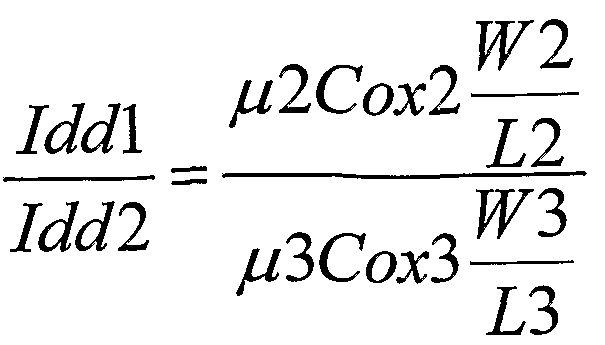
そして、 数式 5において、 制御電流 I d d 'lが常に制御電流 I d d 2よりも 大きいことより、 下記の数式 6を得る (図 2 (b) 参照)。 なお、 数式 6を満 たす場合、 数式 5において、 (; u 2 C o x 2) / (μ 3 C o X 3) がほぼ 1に なるように、 各 μや各 C ο Xを設定する。 すなわち、 例えば、 μ 2 = μ 3、 且 つ、 C ο X 2 =C ο X 3となるように、 各 や各 C o Xを設定する。
そして、 数式 5及ぴ数式 6を満たすように、 W2、 W3、 L 2、 及ぴ L 3を 設定する。 例えば、 I d d l / I d d 2 = 2、 (W 2 / L 2 ) / (W3 L 3 ) = 2、 及ぴ I d d l〉 I d d 2という条件のもとで各 W、 Lを設定すれば、 数式 4が満たされるので、 ダイナミックレンジを等しくすることができる。
このように、 数式 5及ぴ数式 6を満たすように、 トランジスタ 3 2〜3 5の 各グート幅と ^ゲート長を調整することによって、 数式 4を満たすことができ るので、 制御電流 I s sの電流量を変えずに、 従来の利得可変増幅器 7 0のダ イナミックレンジよりもダイナミックレンジを大きくすることができる。 これ より、 出力信号の歪率の悪化を抑えることが可能となる。 また、 トランジスタ 3 2及ぴ 3 3の各ゲート幅又は各ゲート長のみを調整し、 差動増幅回路 1 3の 制御電流を差動増幅回路 1 4に対して相対的に増やすように構成することによ つて、 制御電流 I s sの電流量を増大させないので、 ゲート電圧 V g sが増大 し、 低電圧動作を困難にさせることを抑えることができる。
なお、 利得可変増幅器 1 0において、 差動増幅回路 1 3を構成するトランジ スタ 3 2及び 3 3のそれぞれの WZLは等しく、 また、 差動増幅回路 1 4を構 成するトランジスタ 3 4及び 3 5のそれぞれの W/Lも等しく構成される。 ま
た、 W2ZL 2及び W3/L 3の値が小さいと、 差動増幅回路 13又は 14の グート電圧 V g sが大きくなり、 低い電圧での動作が難しくなつてしまうので、 W2/L 2及び W3/L 3の値は、 できるだけ大きくすることが望ましい。 そ して、 差動増幅回路 13の方の W 2 ZL 2を大きくする場合は、 差動増幅回路 13のゲート電圧 Vg sも差動増幅回路 14のゲート電圧 Vg sも小さくなら ないので、 低電圧動作を困難にさせることを抑えることができる。
【数 6】
W2 W3
L2 L3
また、 上記数式 5において、 制御電流 I d d 1が制御電流 I d d 2よりも大 きいことより下記の数式 7を得る (図 2 (b) 参照)。 なお、 数式 7を満たす 場合、 数式 5において、 (C o X 2 (W 2 / L 2 ) ) / (C o x 3 (W3/L 3)) がほぼ 1になるように、 各 W/Lや各 C o Xを設定する。 すなわち、 例 えば、 (W2/L2) = (W3/L3)、 且つ、 Co x 2 = Co x 3となるよう に、 各 WZLや各 C o Xを設定する。
そして、 数式 5及び数式 7を満たすように、 μ 2及び μ 3を設定する。 例え ば、 I d d lZl d d 2 = 2、 μ 2/ ιχ 3 = 2, 及ぴ I d d l > I d d 2とい う条件のもとで μ 2及び ^ 3を設定すれば、 数式 4が満たされるので、 ダイナ ミックレンジを等しくすることができる。
このように、 数式 5及び数式 7を満たすように、 トランジスタ 32及び 33 の各電子移動度を調整することによって、 数式 4を満たすことができるので、 制御電流 I s sの電流量を変えずに、 従来の利得可変増幅器 70のダイナミツ クレンジよりもダイナミックレンジを大きくすることができる。 これより、 出 力信号の歪率の悪化を抑えることが可能となる。 また、 トランジスタ 32及び 33の各電子移動度のみを調整し、 差動増幅回路 13の制御電流を差動増幅回
路 1 2の制御電流に対して、 相対的に増やすように構成することによって、 低 電圧動作を困難にさせることを抑えることができる。
【数 7】
μ2 > μ3
また、 上記数式 5において、 制御電流 I d d 1が制御電流 I d d 2よりも大 きいことより下記の数式 8を得る (図 2 (b) 参照)。 なお、 数式 8を満たす 場合、 数式 5において、 (μ 2 (W 2 / L 2 ) ) / (μ 3 (W3/L 3)) がほ ぼ 1になるように、 各 W/Lや各 / を設定する。 すなわち、 例えば、 (W2
L 2) = (W 3 / L 3 )、 且つ、 μ 2 = μ 3となるように、 各 W/Lや各 μを 設定する。 ' そして、 数式 5及び数式 8を満たすように、 C ο X 2及ぴ C ο X 3を設定す る。 例えば、 I d d l/ I d d 2 = 2、 C o x 2/C o x 3 = 2、 及ぴ I d d 1 > I d d 2という条件のもとで C o x 2及び C o x 3を設定すれば、 数式 4 が満たされるので、 ダイナミックレンジを等しくすることができる。
このように、 数.式 5及び数式 8を満たすように、 トランジスタ 3 2及ぴ 3 3 の各グート酸化膜容量を調整することによって、 数式 4を満たすことができる ので、 制御電流 I s sの電流量を変えずに、 従来の利得可変増幅器 7 0のダイ ナミックレンジよりもダイナミックレンジを大きくすることができる。 これよ り、 出力信号の歪率の悪化を抑えることが可能となる。 また、 トランジスタ 3 2及び 3 3の各グート酸化膜容量のみを調整し、 差動増幅回路 1 3の制御電流 を相対的に増やすように構成することによって、 低電圧動作を困難にさせるこ とを抑えることができる。
【数 8】
Cox2 > Cox3
このように、 差動増幅回路 1 3及ぴ 1 4のそれぞれのダイナミックレンジが
等しくなるように、 差動増幅回路 1 3を構成するトランジスタのゲート幅 ゲ ート長の値を、 差動増幅回路 1 4を構成するトランジスタのゲート幅 Zゲート 長の値よりも大きくしたり、 また、 差動増幅回路 1 3を構成するトランジスタ の電子移動度を、 差動増幅回路 1 4を構成するトランジスタの移動度よりも大 きくしたり、 また、 差動増幅回路 1 3を構成するトランジスタのゲート酸化膜 容量を、 差動増幅回路 1 4を構成するトランジスタのゲート酸化膜容量よりも 大きくしたりすることによって、 消費電流を変えずに、 且つ、 低電圧動作を困 難にさせずに、 出力信号の歪率の悪化を抑えることが可能となる。
また、 I d d 1 > I d d 2という条件を満たしつつ、 差動増幅回路 1 3及ぴ 1 4のそれぞれのダイナミックレンジが等しくなるように制御電流 I d d 2を 増加させてもよい。 すなわち、 下記の数式 9が示すように、 制御電流 I d d 2 に電流 I αを加えることによって、 その制御電流 I (1 (1 2 +電流1 αの電流量 が制御電流 I d d 1の電流量と等しくなるように、 差動増幅回路 1 4に流す電 流の量を増加させてもよい。
【数 9】 .
Iddl = Iddl + la (但し、 腿 > Iddl)
図 5は、 上記数式 9を満たすための他の実施形態である利得可変増幅器 4 0 を示す図である。
図 5に示す利得可変増幅器 4 0の差動増幅回路 1 4には、 制御電流 I d d 2 の他に電流 I ο;を流すための定電流源 4 1 (第 2の定電流源) が接続されてい る。
このように、 差動増幅回路 1 4に定電流原4 1を設け、 差動増幅回路 1 3及 び 1 4のそれぞれのダイナミックレンジを等しくさせることにより、 従来の利 得可変増幅器 7 0全体のダイナミックレンジよりも本実施形態の利得可変増幅 器 4 0全体のダイナミックレンジを大きくすることができ、 出力信号の歪率の
悪化を抑えることが可能となる。
また、 図 6は、 図 4の利得可変増幅器 1 0における各差動増幅回路の他の接 続構成を示す図である。
図 6に示すように、 利得可変増幅器 5 0は、 差動増幅回路 1 2の出力部に、 トランジスタ 5 1から構成するカレントミラー回路 5 2 (破線部 D) を設け、 差動増幅回路 1 3及び 1 4を電源側に折り返している。
このように、 カレントミラー回路 5 2で差動増幅回路 1 3及び 1 4を電源側 に折り返すことによって、 電源〜グラウンド (g n d ) 間に縦につながるトラ ンジスタの段数を少なくすることができるので、 利得可変増幅器 1 0のダイナ ミックレンジを更に大きくすることが可能となる。
また、 他に電¾1〜グラウンド間に縦につながるトランジスタの段数を少なく する構成として、 図 7のように構成することができる。
図 7は、 図 4の利得可変増幅器 1 0における各差動増幅回路の他の接続構成 を示す図である。
図 7に示すように、 利得可変増幅器 6 0は、 差動増幅回路 1 2の出力部に、 トランジスタ 6 1から構成されるフォールテツドカスコード回路 6 2 (破線部 E ) を設け、 差動増幅回路 1 3及び 1 4を電源側に折り返している。
このように、 フォールテツドカスコード回路 6 2で差動増幅回路 1 3及ぴ 1 4を電源側に折り返すことによって、 電源〜グラウンド間に縦につながるトラ ンジスタの段数を少なくすることができるので、 利得可変増幅器 1 0のダイナ ミックレンジを更に大きくすることが可能となる。
なお、 本実施形態の利得可変増幅器 1 0では、 差動増幅回路 1 3を構成する トランジスタ 3 2及び 3 3のそれぞれの W/ Lや差動増幅回路 1 4を構成する トランジスタ 3 4及び 3 5のそれぞれの W/ Lを等しい比率で構成しているが、 上記数式 4のように、 差動増幅回路 1 3のダイナミックレンジと差動増幅回路
1 4のダイナミックレンジとが等しく構成できれば、 トランジスタ 3 2〜3 5 の個々の WZ Lの比率は特に限定されない。 すなわち、 差動増幅回路 1 3及ぴ 差動増幅回路 1 4のそれぞれのダイナミックレンジを等しくなるように構成す ることができれば、 例えば、 トランジスタ 3 2の W/ Lとトランジスタ 3 3の W/ Lとを異なる大きさに設定してもよい。
しかしながら、 トランジスタ 3 2〜3 5のそれぞれの W/ Lの大きさを異な る大きさで構成するよりも、 上述の本実施形態の利得可変増幅器のように、 ト ランジスタ 3 2及び 3 3のそれぞれの WZ Lの比率が等しくなるように差動增 幅回路 1 4を構成し、 トランジスタ 3 4及び 3 5のそれぞれの W/ Lの比率が 等しくなるように差動増幅回路 1 4を構成する方が、 各トランジスタを製造す る際の半導体製造工程を簡単にすることができる。
また、 本実施形態の利得可変増幅器 1 0では、 差動増幅回路 1 2、 1 3及ぴ 1 4を MO S F E Tで構成しているが、 バイポーラトランジスタで差動増幅回 路 1 2、 1 3、 及び 1 4を構成してもよく、 この場合、 差動増幅回路 1 3及ぴ 1 4を構成す.るそれぞれのバイポーラトランジスタのエミッタサイズ比を変更 することによって、 差動増幅回路 1 3及ぴ差動増幅回路 1 4のそれぞれのダイ ナミックレンジを等しくさせる。
本発明の利得可変増幅器によれば、 利得が 0以外の最小利得時において、 入 力信号が入力される 2つの差動増幅回路のそれぞれのダイナミックレンジを等 しくすることで、 利得可変増幅器全体のダイナミックレンジを従来の利得可変 増幅器全体のダイナミックレンジよりも大きくすることができるので、 出力信 号の歪率の悪化を抑えることが可能となる。
また、 2つの差動増幅回路の内の一方の差動増幅回路の制御電流を他方の差 動増幅回路の制御電流よりも相対的に増やすことによって、 2つの差動増幅回 路のそれぞれのダイナミックレンジを等しくさせるので、 消費電流の増大を抑
えつつ、 低電圧動作を困難にさせることを抑えることができる。
Claims
1 . 入力信号に基づいて利得を可変し、 出力信号の出力レベルを一定に保つ 利得可変増幅器であって、
上記入力信号が入力される 2つの差動增幅回路のそれぞれのダイナミックレ ンジが等しいことを特徴とする利得可変増幅器。
2. 請求の範囲第 1項に記載の利得可変増幅回路であって、
当該利得可変増幅器の利得が 0以外の最小利得において、 一方の差動増幅回 路の制御電流を他方の差動増幅回路の制御電流に対して相対的に増加させて、 上記 2つの差動増幅回路のそれぞれのダイナミックレンジが等しくなるように 設定されることを特徴とする利得可変増幅器。
3 . 2つのトランジスタを備え、 利得を可変するための制御信号が入力され る第 1の差動増幅回路と、 . . 上記第 1の差動増幅回路を駆動するための電流を生成する第 1の定電流源と、 2つのトランジスタを備え、 上記第 1の定電流源が生成する電流を所定の比 で分けた内の大きい比の電流により駆動し、 入力信号を上記制御信号に基づい て増幅する第 2の差動増幅回路と、
2つのトランジスタを備え、 上記所定の比で分けた電流の内の小さい電流に より駆動し、 入力信号を上記制御信号に基づいて増幅する第 3の差動増幅回路 と、
を備え、
上記第 2の差動増幅回路のダイナミックレンジと上記第 3の差動増幅回路の ダイナミックレンジとが等しいことを特徴とする利得可変増幅器。
4 . 請求の範囲第 3項に記載の利得可変増幅器であって、 上記第 2の差動増幅回路のゲート幅とゲート長との比率が、 上記第 3の差動 増幅回路のゲート幅とゲート長との比率より大きく、 上記第 2の差動増幅回路 のダイナミックレンジと上記第 3の差動増幅回路のダイナミックレンジとが等 しいことを特徴とする利得可変増幅器。
5 . 請求の範囲第 3項に記載の利得可変増幅器であって、
上記第 2の差動増幅回路の電子移動度が、 上記第 3の差動増幅回路の電子移 動度より大きく、 上記第 2の差動増幅回路のダイナミックレンジと上記第 3の 差動増幅回路のダイナミックレンジとが等しいことを特徴とする利得可変増幅
6 . 請求の範囲第 3項に記載の利得可変増幅器であって、
上記第 2の差動増幅回路のゲート酸化膜容量が、 上記第 3の差動増幅回路の グート酸化 S莫容量より大きく、 上記第 2の差動増幅回路のダイナミックレンジ と上記第 3の差動増幅回路のダイナミックレンジとが等しいことを特徴とする 利得可変増幅器。 7 · 請求の範囲第 3項に記載の利得可変増幅器であって、
上記第 2の差動増幅回路を駆動させる電流比と、 上記第 3の差動増幅回路を 駆動させる電流比とを等しくさせる電流を生成する第 2の定電流源を上記第 3 の差動増幅回路に接続することを特徴とする利得可変増幅器。
Applications Claiming Priority (2)
| Application Number | Priority Date | Filing Date | Title |
|---|---|---|---|
| JP2002221063A JP2004064491A (ja) | 2002-07-30 | 2002-07-30 | 利得可変増幅器 |
| JP2002-221063 | 2002-07-30 |
Publications (1)
| Publication Number | Publication Date |
|---|---|
| WO2004012329A1 true WO2004012329A1 (ja) | 2004-02-05 |
Family
ID=31184830
Family Applications (1)
| Application Number | Title | Priority Date | Filing Date |
|---|---|---|---|
| PCT/JP2003/008770 Ceased WO2004012329A1 (ja) | 2002-07-30 | 2003-07-10 | 利得可変増幅器 |
Country Status (3)
| Country | Link |
|---|---|
| JP (1) | JP2004064491A (ja) |
| TW (1) | TW200405655A (ja) |
| WO (1) | WO2004012329A1 (ja) |
Families Citing this family (1)
| Publication number | Priority date | Publication date | Assignee | Title |
|---|---|---|---|---|
| JP5293411B2 (ja) * | 2009-06-01 | 2013-09-18 | ソニー株式会社 | 受信装置 |
Citations (2)
| Publication number | Priority date | Publication date | Assignee | Title |
|---|---|---|---|---|
| JPH05259769A (ja) * | 1992-03-16 | 1993-10-08 | Nippon Telegr & Teleph Corp <Ntt> | 可変利得増幅回路 |
| JP2000013159A (ja) * | 1998-06-26 | 2000-01-14 | Sony Corp | 増幅回路 |
-
2002
- 2002-07-30 JP JP2002221063A patent/JP2004064491A/ja not_active Withdrawn
-
2003
- 2003-07-10 WO PCT/JP2003/008770 patent/WO2004012329A1/ja not_active Ceased
- 2003-07-29 TW TW92120594A patent/TW200405655A/zh unknown
Patent Citations (2)
| Publication number | Priority date | Publication date | Assignee | Title |
|---|---|---|---|---|
| JPH05259769A (ja) * | 1992-03-16 | 1993-10-08 | Nippon Telegr & Teleph Corp <Ntt> | 可変利得増幅回路 |
| JP2000013159A (ja) * | 1998-06-26 | 2000-01-14 | Sony Corp | 増幅回路 |
Also Published As
| Publication number | Publication date |
|---|---|
| JP2004064491A (ja) | 2004-02-26 |
| TW200405655A (en) | 2004-04-01 |
Similar Documents
| Publication | Publication Date | Title |
|---|---|---|
| US7782136B2 (en) | Digitally adjusted variable gain amplifier (VGA) using switchable differential pairs | |
| US20100301939A1 (en) | High frequency receiver preamplifier | |
| US6714076B1 (en) | Buffer circuit for op amp output stage | |
| US20020163384A1 (en) | Transconductor and filter circuit using the same | |
| US20070176683A1 (en) | Variable gain amplifier | |
| US8711024B2 (en) | Switched capacitor amplifier | |
| EP2645565A1 (en) | A fully differential amplifier topology to drive dynamic speakers in class AB mode | |
| US8416969B2 (en) | Amplifier circuit | |
| JP7278306B2 (ja) | Ab級アンプおよびオペアンプ | |
| US8674743B1 (en) | Asymmetric correction circuit with negative resistance | |
| US20060012431A1 (en) | Class AB amplifier having adjustable quiescent current and output current | |
| US5825228A (en) | Low quiescent power, high output power rail-to rail amplifier output stages and methods for using same | |
| US8400214B2 (en) | Class AB output stage | |
| US20080197928A1 (en) | Threshold voltage compensation for a two stage amplifier | |
| US6919767B2 (en) | Circuit arrangement for low-noise fully differential amplification | |
| US7394316B1 (en) | High speed, high current gain voltage buffer and method | |
| US20070132494A1 (en) | Duty cycle correction amplification circuit | |
| WO2004012329A1 (ja) | 利得可変増幅器 | |
| US8385016B1 (en) | Asymmetric correction circuit | |
| JP2007221402A (ja) | 可変利得増幅器及びその半導体集積装置 | |
| US7609112B2 (en) | Boosted tail-current circuit | |
| JP2006270442A (ja) | フィルタ回路のq補正 | |
| CN101416386A (zh) | 高线性可变增益放大器 | |
| US6784733B1 (en) | Dynamically controlled amplifier | |
| US7667540B2 (en) | Class-AB driver design with improved frequency response |
Legal Events
| Date | Code | Title | Description |
|---|---|---|---|
| AK | Designated states |
Kind code of ref document: A1 Designated state(s): CN KR US |
|
| AL | Designated countries for regional patents |
Kind code of ref document: A1 Designated state(s): AT BE BG CH CY CZ DE DK EE ES FI FR GB GR HU IE IT LU MC NL PT RO SE SI SK TR |
|
| 121 | Ep: the epo has been informed by wipo that ep was designated in this application | ||
| 122 | Ep: pct application non-entry in european phase |