WO2003104861A1 - Semi-transparent semi-reflective liquid crystal display device color filter - Google Patents
Semi-transparent semi-reflective liquid crystal display device color filter Download PDFInfo
- Publication number
- WO2003104861A1 WO2003104861A1 PCT/JP2003/005785 JP0305785W WO03104861A1 WO 2003104861 A1 WO2003104861 A1 WO 2003104861A1 JP 0305785 W JP0305785 W JP 0305785W WO 03104861 A1 WO03104861 A1 WO 03104861A1
- Authority
- WO
- WIPO (PCT)
- Prior art keywords
- layer
- optical path
- liquid crystal
- path difference
- reflected light
- Prior art date
Links
Classifications
-
- G—PHYSICS
- G02—OPTICS
- G02B—OPTICAL ELEMENTS, SYSTEMS OR APPARATUS
- G02B5/00—Optical elements other than lenses
- G02B5/20—Filters
- G02B5/201—Filters in the form of arrays
-
- G—PHYSICS
- G02—OPTICS
- G02F—OPTICAL DEVICES OR ARRANGEMENTS FOR THE CONTROL OF LIGHT BY MODIFICATION OF THE OPTICAL PROPERTIES OF THE MEDIA OF THE ELEMENTS INVOLVED THEREIN; NON-LINEAR OPTICS; FREQUENCY-CHANGING OF LIGHT; OPTICAL LOGIC ELEMENTS; OPTICAL ANALOGUE/DIGITAL CONVERTERS
- G02F1/00—Devices or arrangements for the control of the intensity, colour, phase, polarisation or direction of light arriving from an independent light source, e.g. switching, gating or modulating; Non-linear optics
- G02F1/01—Devices or arrangements for the control of the intensity, colour, phase, polarisation or direction of light arriving from an independent light source, e.g. switching, gating or modulating; Non-linear optics for the control of the intensity, phase, polarisation or colour
- G02F1/13—Devices or arrangements for the control of the intensity, colour, phase, polarisation or direction of light arriving from an independent light source, e.g. switching, gating or modulating; Non-linear optics for the control of the intensity, phase, polarisation or colour based on liquid crystals, e.g. single liquid crystal display cells
- G02F1/133—Constructional arrangements; Operation of liquid crystal cells; Circuit arrangements
- G02F1/1333—Constructional arrangements; Manufacturing methods
- G02F1/1335—Structural association of cells with optical devices, e.g. polarisers or reflectors
- G02F1/133553—Reflecting elements
- G02F1/133555—Transflectors
-
- C—CHEMISTRY; METALLURGY
- C09—DYES; PAINTS; POLISHES; NATURAL RESINS; ADHESIVES; COMPOSITIONS NOT OTHERWISE PROVIDED FOR; APPLICATIONS OF MATERIALS NOT OTHERWISE PROVIDED FOR
- C09K—MATERIALS FOR MISCELLANEOUS APPLICATIONS, NOT PROVIDED FOR ELSEWHERE
- C09K2323/00—Functional layers of liquid crystal optical display excluding electroactive liquid crystal layer characterised by chemical composition
- C09K2323/03—Viewing layer characterised by chemical composition
- C09K2323/031—Polarizer or dye
-
- G—PHYSICS
- G02—OPTICS
- G02F—OPTICAL DEVICES OR ARRANGEMENTS FOR THE CONTROL OF LIGHT BY MODIFICATION OF THE OPTICAL PROPERTIES OF THE MEDIA OF THE ELEMENTS INVOLVED THEREIN; NON-LINEAR OPTICS; FREQUENCY-CHANGING OF LIGHT; OPTICAL LOGIC ELEMENTS; OPTICAL ANALOGUE/DIGITAL CONVERTERS
- G02F1/00—Devices or arrangements for the control of the intensity, colour, phase, polarisation or direction of light arriving from an independent light source, e.g. switching, gating or modulating; Non-linear optics
- G02F1/01—Devices or arrangements for the control of the intensity, colour, phase, polarisation or direction of light arriving from an independent light source, e.g. switching, gating or modulating; Non-linear optics for the control of the intensity, phase, polarisation or colour
- G02F1/13—Devices or arrangements for the control of the intensity, colour, phase, polarisation or direction of light arriving from an independent light source, e.g. switching, gating or modulating; Non-linear optics for the control of the intensity, phase, polarisation or colour based on liquid crystals, e.g. single liquid crystal display cells
- G02F1/133—Constructional arrangements; Operation of liquid crystal cells; Circuit arrangements
- G02F1/1333—Constructional arrangements; Manufacturing methods
- G02F1/1335—Structural association of cells with optical devices, e.g. polarisers or reflectors
- G02F1/133509—Filters, e.g. light shielding masks
- G02F1/133514—Colour filters
Definitions
- the present invention relates to a color filter for a transflective color liquid crystal display device used in a transflective color liquid crystal display device.
- transmissive liquid crystal display device As a transmissive liquid crystal display device, a transmissive liquid crystal display device in which a backlight is arranged on the back or side of the electrode substrate located on the back side and color display is performed using this as a light source has been widely spread. are doing.
- liquid crystal display devices have been expected to be used for portable display devices such as mopile devices, taking advantage of their features of low power consumption and light weight.
- portable display devices such as mopile devices
- the power consumption of the built-in light source is large, so that the battery usage time is short and the device occupies a large proportion, making the device heavy and bulky. There was such a problem.
- This reflective color liquid crystal display device can achieve low power consumption because it does not include a backlight, and can be made small, light, and thin, and is suitable as a portable display device.
- the transmissive color liquid crystal display device has a remarkably reduced display effect under strong external light such as outdoors, whereas the reflective color liquid crystal display device has a much better display effect.
- a reflective color liquid crystal display device does not function at all, whereas a transmissive color liquid crystal display device has a darker periphery, thereby further increasing visibility.
- a transflective liquid crystal display device having the functions of a transmissive liquid crystal display device and a reflective liquid crystal display device has been provided, and even in the presence of strong external light such as outdoors, It is suitably used for portable terminals and the like that are to be used even in places where external light is scarce (Japanese Patent Application Laid-Open Nos. 2002-34031 and 2002-35) No. 08284).
- the thickness of the colored layer can be reduced by half.
- the transparent electrode made of ITO or the like formed on the color filter is disconnected, and the gap is not constant.
- the present invention has been made in view of the above problems, is easy to manufacture, and is capable of displaying in the same color tone even if it is reflected light or transmitted light. It is a primary object of the present invention to provide a color filter for a liquid crystal display device. To achieve the above object, the present invention provides a transparent substrate, a transparent film pattern layer in which a transparent film is formed in a pattern on the transparent substrate, and a transparent film pattern layer formed so as to cover the transparent film pattern layer.
- a color filter for a transflective liquid crystal display device having a transparent film pattern region in which a colored layer is laminated.
- the transparent film pattern region in which the transparent film is formed in a pattern on the transparent substrate it is possible to adjust the color characteristics of the reflected light region or the transmitted light region, Since the color characteristics of the reflected light region and the transmitted light region are equal, it is possible to provide a color filter for a transflective liquid crystal display device.
- the transparent film pattern region is used as a region for reflected light, and a colored layer region having the transparent substrate and a colored layer formed on the transparent substrate is transmitted through a colored layer region. It can be used for the application area.
- the transparent film pattern region has a transparent film pattern with respect to the colored layer region having no transparent film, the color purity is reduced as compared with the transmitted light of the colored layer alone. This makes it possible to obtain the same color characteristics as when a pack light has passed through the colored layer region once even when external light has passed through the transparent film pattern region twice.
- this transparent film pattern region as the region for reflected light, it is possible to make the color characteristics of the region for reflected light equal to the color characteristics in the region for transmitted light.
- the transparent film pattern region is used as a region for transmitted light, the transparent substrate, a transparent film uniform layer in which a transparent film is uniformly formed on the transparent substrate, and a transparent film uniform layer.
- a transparent film uniform region formed by laminating a colored layer having one layer formed thereon may be used as the reflected light region.
- the transparent film is formed in a pattern, and in the transparent film uniform region, since the transparent film is formed uniformly on the entire surface, the transparent film uniform region is the transparent film pattern region.
- the effect of the transparent film is greater than that of, and the color purity when light is transmitted can be reduced. This makes it possible to obtain the same color characteristics when the backlight passes through the transparent film pattern region once and when the outside light passes through the transparent film uniform region twice.
- the area as the area for reflected light and the transparent film pattern area as the area for transmitted light, it is possible to approximate the color characteristics in the area for transmitted light and the area for reflected light.
- the film thickness is set to the transparent film pattern region having the pattern on the transparent substrate. It can be made uniform.
- the area ratio of the area where the transparent film is formed in the above-mentioned transparent film pattern area is best in the above range ⁇ ⁇ ⁇ ⁇ in the current processing accuracy, and the colors of the reflected light area and the transmitted light area are the best. It is possible to make the characteristics closest.
- the area ratio of the region where the transparent film is formed in the transparent film pattern region is smaller than the above range, it is difficult to make the film thickness in the reflected light region and the transmitted light region uniform. If it is larger than the above range, it is difficult to make the color characteristics close to each other.
- the thickness of the transparent film forming the transparent film pattern layer and the transparent film uniform layer is the thickness of the colored layer in the case where the colored layer is used only in the colored layer in the transmitted light region.
- the film thickness is 1, the film thickness is preferably in the range of 0.5 to 3.0.
- the film thickness of the transparent film pattern layer and the transparent film forming the transparent film uniform layer is within the above range, and is the area ratio of the transparent film forming region in the transparent film pattern region described above. In this case, the color characteristics in the reflected light area and the transmitted light area can be made closer.
- the transparent film pattern layer has a pattern in which the transparent film is formed in an island shape
- the transparent film pattern layer has a hole formed in the transparent film in a pattern shape. It may have a pattern consisting of: These are appropriately selected and used depending on the device and conditions at the time of manufacturing.
- an island-shaped portion or a hole of the transparent film pattern layer is formed in a circular shape. Since the island-shaped portions or holes of the transparent film pattern layer are formed in a circular shape, the above-described area ratio adjustment and design can be performed during the production of the transflective color filter. This facilitates pattern formation, and is preferable from the viewpoint of manufacturing efficiency and the like.
- the thickness of the transparent film pattern layer, or the transparent film forming the transparent film pattern layer and the transparent film uniform layer may be 0.5 to 3.5 ⁇ . preferable.
- the transparent film preferably has a spectral transmittance at a wavelength of 380 nm to 780 nm of 85% or more.
- the color filter for the transflective liquid crystal display device of the present invention hardly affects the color characteristics and the like of the colored layer. This is because the color characteristics of the transmission area and the transmitted light area can be made closer to each other.
- the present invention provides a transflective liquid crystal display device including the color filter for a transflective liquid crystal display device according to the first embodiment or the second embodiment.
- the present invention it is possible to provide a liquid crystal display device having the same color characteristics in the transmitted light region and the reflected light region by including the above-mentioned transflective filter for a transflective liquid crystal display device. It is.
- the present invention provides, in the third embodiment, a color filter for a transflective liquid crystal display device having a transparent substrate, and a colored layer for reflected light and a colored layer for transmitted light formed on the transparent substrate.
- the colored layer for reflected light is formed such that a concave and convex portion is formed on the liquid crystal layer side surface, and the average film thickness is smaller than the thickness of the colored layer for transmitted light.
- a transflective liquid crystal having a refractive index difference of 0.1 or more between a colored layer for reflection and a layer in contact with a surface of the colored layer for reflected light on a side on which the convexity is formed.
- a color filter for a display device Provided is a color filter for a display device.
- irregularities are formed on the surface of the colored layer for reflected light, the difference in refractive index between adjacent layers is set to 0.1 or more, and the average film thickness is determined by the thickness of the colored layer for transmitted light. Only by reducing the thickness, the light scattering effect on the reflected light and the similar color tone between the reflected light and the transmitted light can be simultaneously achieved. Therefore, it is possible to easily form a color filter for a transflective liquid crystal display device in a simple and cost-effective manner.
- the reflective light colored layer, the refractive index difference between the layer that is in contact with the surface of the reflective light colored layer on the side of the unevenness is formed to be 0.1 or more
- the colored layer for reflected light contains a refractive index increasing agent for increasing the refractive index.
- the concave and convex portions on the surface of the colored layer for reflected light are formed with a plurality of concave portions each having a curved surface on the surface of the colored layer for reflected light formed with the same film thickness as the coloring layer for transmitted light. It is preferred that it is formed by. If the concave and convex portions on the surface of the colored layer for reflected light are formed into a plurality of turns formed by curved surfaces, it is possible to form the concave and convex portions more easily by performing one photolithography method. It is easy to control the average thickness of the colored layer for light, so it is possible to easily adjust the difference in thickness between the colored layer for transmitted light and the color tone of reflected light and transmitted light. The same can easily be achieved.
- the layer in contact with the surface of the colored layer for reflected light on which the irregularities are formed is an optical path difference adjusting layer for adjusting the optical path difference between the reflected light region and the transmitted light region. It is preferred that Since the reflected light passes through the liquid crystal layer twice as long as the transmitted light, it is necessary to adjust this optical path difference. Therefore, it is preferable that an optical path difference adjusting layer for adjusting such an optical path difference is formed on the reflected light colored layer.
- a color filter for a transflective color liquid crystal display device having a transparent substrate, and a colored layer for reflected light and a colored layer for transmitted light formed on the transparent substrate.
- the colored layer for reflected light has irregularities formed on the liquid crystal layer side surface, and is formed so that the average film thickness is smaller than the thickness of the colored layer for transmitted light.
- An optical path difference adjustment layer for adjusting an optical path difference between the reflected light area and the transmitted light area is formed on the surface on the side where the unevenness is formed, and the reflected light coloring layer and the optical path difference adjustment are formed.
- the optical path difference is set so that the refractive index difference with the layer is 0.1 or more.
- a color filter for a transflective color liquid crystal display device characterized in that the adjustment layer contains a refractive index increasing agent for increasing the refractive index.
- the refractive index of the optical path difference adjusting layer can be easily increased by adding a refractive index increasing agent to the optical path difference adjusting layer, when selecting a material for forming the optical path difference adjusting layer, You can expand your options. As a result, cost reduction can be achieved.
- the unevenness on the surface of the colored layer for reflected light is obtained by forming a plurality of concave portions having curved surfaces on the surface of the colored layer for reflected light formed with the same thickness as the colored layer for transmitted light.
- the irregularities on the surface of the colored layer for reflected light are formed into a plurality of concaves constituted by curved surfaces, it is possible to easily form the irregularities by performing a photolithography method. It is easy to control the average film thickness of the layer, and it is possible to easily adjust the difference in film thickness between the transmitted light colored layer and the reflected light and the transmitted light. It can be.
- a convex is formed on the liquid crystal layer side surface of the optical path difference adjustment layer, and the optical path difference adjustment layer and the surface of the optical path difference adjustment layer on which the unevenness is formed are formed on the surface.
- the difference in the refractive index from the contacting layer is 0.1 or more.
- the irregularities on the surface of the optical path difference adjustment layer are formed by forming a plurality of concave portions having curved surfaces on the surface of the optical path difference adjustment layer. This is because such a concave portion can be easily formed, and the shape can be adjusted relatively easily.
- the color for a transflective liquid crystal display device comprising a transparent substrate, and a colored layer for reflected light and a colored layer for transmitted light formed on the transparent substrate.
- the reflected light colored layer is formed such that irregularities are formed on a surface of the liquid crystal layer side, and the average film thickness is smaller than the thickness of the transmitted light colored layer.
- An optical path difference adjustment layer for adjusting the optical path difference between the reflected light area and the transmitted light area is formed on the surface of the colored layer for use in which the unevenness is formed, and the liquid crystal layer side of the optical path difference adjustment layer is formed.
- Irregularities are also formed on the surface, and irregularities of the optical path difference adjustment layer are formed.
- the flattened layer for the optical path difference adjusting layer is formed on the surface on the side where the optical path difference adjusting layer is flattened, and the optical path difference adjusting layer and the flattening layer for the optical path difference adjusting layer are refracted.
- a transflective power filter for a liquid crystal display device characterized in that the rate difference is 0.1 or more.
- the light scattering effect can be more effectively obtained by forming the concave and convex portions on both the surface of the colored layer for reflected light and the surface of the optical path difference adjusting layer.
- the optical path difference adjusting layer and the planarizing layer for the optical path difference adjusting layer have a refractive index such that the refractive index difference between the optical path difference adjusting layer and the planarizing layer for the optical path difference adjusting layer is 0.1 or more. It is preferable to include a refractive index increasing agent for increasing the refractive index.
- a refractive index additive to the flattening layer for the optical path difference adjusting layer, it becomes easy to adjust the refractive index difference between the optical path difference adjusting layer and the flattening layer for the optical path difference adjusting layer, and to form both layers. This is because it is not necessary to consider the refractive indices of both materials when selecting the material, so that the range of material selection can be expanded.
- the colored layer for reflected light also contains a refractive index increasing agent for increasing the refractive index.
- a refractive index increasing agent also to the colored layer for reflected light, the difference in refractive index between the colored layer for reflected light and the optical path difference adjusting layer, and the planarization for the optical path difference adjusting layer and the optical path difference adjusting layer. It is easy to adjust the refractive index difference between the layers and the material for each layer can be selected without considering such a refractive index difference, so that the range of material selection can be greatly expanded, and the cost can be reduced. It is because it can aim at.
- a plurality of HQ portions each having a curved surface are formed on the surface of the colored layer for reflected light having the same thickness as the colored layer for transmitted light. It is preferred that it is formed by. If the unevenness on the surface of the colored layer for reflected light is made into a plurality of concaves constituted by curved surfaces, it is possible to easily form a rounded convex by performing one photolithography method. Since the average thickness of the colored layer can be easily controlled, it is possible to easily adjust the thickness difference between the colored layer for transmitted light and the color tone of reflected light and transmitted light. The same can be easily achieved.
- the unevenness of the surface of the optical path difference adjusting layer It is preferable that a plurality of concave portions formed of curved surfaces are formed on the surface of the adjustment layer. This is because such a concave portion can be easily formed and its shape can be adjusted relatively easily.
- a color filter for a transflective liquid crystal display device having a transparent substrate and a colored layer for reflected light and a colored layer for transmitted light formed on the transparent substrate according to the sixth embodiment. Wherein at least one removed portion is formed so that the average thickness of the colored layer for reflected light is smaller than the thickness of the colored layer for transmitted light, and the liquid crystal layer of the colored layer for reflected light is formed.
- An optical path difference adjusting layer for adjusting an optical path difference between the reflected light area and the transmitted light area is formed on the side surface, and irregularities are formed on the liquid crystal layer side surface of the optical path difference adjusting layer.
- a transflective liquid crystal display characterized in that the difference in refractive index between the difference adjusting layer and the layer in contact with the surface of the optical path difference adjusting layer on the side where the convexity is formed is 0.1 or more.
- a color filter for a device is provided.
- the refractive index difference from the layer in contact with the surface on the side where the unevenness is formed is formed only by forming the concave and convex portions on the optical path difference adjustment layer surface required for the optical path difference adjustment. 0.1 or more, and a light scattering effect can be obtained in this portion. Therefore, a color filter for a transflective color liquid crystal display device can be obtained relatively easily.
- the optical path difference adjustment layer, the refractive index difference between the layer that contacts the surface of the optical path difference adjustment layer on the side where the unevenness is formed is 0.1 or more
- the optical path difference adjusting layer contains a refractive index increasing agent for increasing the refractive index.
- a refractive index increasing agent By including a refractive index increasing agent, the difference in refractive index between the layer in contact with the surface on which unevenness is formed and the surface in contact with the surface can be easily adjusted to 0.1 or more. This is because the range of selection of a material for forming a layer in contact with the surface on the side where the four protrusions are formed is widened.
- the convex portion on the surface of the optical path difference adjustment layer is formed by forming a plurality of concave portions having curved surfaces on the surface of the optical path difference adjustment layer. This is because such a concave portion can be easily formed, and the shape can be adjusted relatively easily.
- a transparent substrate is formed on the transparent substrate.
- a color filter for a transflective color liquid crystal display device having a colored layer for reflected light and a colored layer for transmitted light, wherein the colored layer for reflected light has an average film thickness of the colored layer for transmitted light. At least one removed portion is formed so as to be thinner, and an optical path difference adjusting layer for adjusting the optical path difference between the reflected light region and the transmitted light region is provided on the surface of the colored layer for reflected light on the liquid crystal layer side.
- the optical path difference adjusting layer is formed with a convex on the liquid crystal layer side surface, and the surface of the optical path difference adjusting layer on which the unevenness is formed has flatness on the surface of the optical path difference adjusting layer.
- the difference in refractive index between the optical path difference adjustment layer and the flattening layer for the optical path difference adjustment layer is 0.1 or more.
- a color filter for a liquid crystal display device By providing the flattening layer for the optical path difference adjustment layer in this way, when forming a transparent electrode layer or the like on the side of the optical path difference adjustment layer where the unevenness is formed, it does not cause inconvenience such as disconnection.
- the transparent electrode layer can be formed in a good state.
- the optical path difference adjusting layer and the planarizing layer for the optical path difference adjusting layer have a refractive index difference of 0.1 or more.
- a refractive index increasing agent for increasing the refractive index is contained.
- the same effect as in the case of the above-described sixth embodiment can also be obtained by including a refractive index increasing agent in the planarizing layer for an optical path difference adjusting layer.
- the unevenness on the surface of the optical path difference adjustment layer is formed by forming a plurality of concave portions having curved surfaces on the surface of the optical path difference adjustment layer. This is because such a concave portion can be easily formed, and the shape can be adjusted relatively easily.
- the present invention further provides a transflective color liquid crystal display device comprising any one of the color filters for transflective color liquid crystal display devices according to the third embodiment to the seventh embodiment. .
- the cost can be reduced.
- FIG. 1 is a diagram showing an example of the transflective color filter of the present invention.
- FIG. 2 is a diagram showing another example of the transflective color filter of the present invention.
- FIG. 3 is a diagram showing an example of a transparent film pattern in the transparent film pattern region of the present invention.
- FIG. 4 is a diagram showing another example of the pattern of the transparent film in the transparent film pattern region of the present invention.
- FIG. 5 is a diagram showing another example of the pattern of the transparent film in the transparent film pattern region of the present invention.
- FIG. 6 is a view showing another example of the pattern of the transparent film in the transparent film pattern region of the present invention.
- FIG. 7 is a diagram illustrating an example of a light transmission path of the transflective color filter of the present invention. '
- FIG. 8 is a diagram showing an example of a simulation for obtaining an optimum value of the transflective color filter of the present invention.
- FIG. 9 is a diagram showing an example of a transparent film pattern in the transparent film pattern region of the present invention.
- FIG. 10 is a diagram showing the area ratio of the transparent film pattern region in the whole of the present invention.
- FIG. 11 is a diagram showing an example of a transflective color filter according to an embodiment of the present invention.
- FIG. 12 is a diagram showing an example of a conventional transflective color filter.
- FIG. 13 is a schematic sectional view showing an example of the transflective color filter of the present invention.
- FIG. 14 is a schematic sectional view showing another example of the transflective color filter of the present invention.
- FIG. 15 is a schematic sectional view showing another example of the transflective filter of the present invention.
- FIG. 16 is a schematic sectional view showing another example of the transflective color filter of the present invention.
- FIG. 17 is a schematic view showing an example of a mask used for confirming the effect of the uneven shape in the example.
- FIG. 18 shows the measurement results of the haze in the confirmation of the effect of the uneven shape in the example ⁇ s.
- Figure 19 shows the results of measuring the haze in confirming the effect of the uneven shape in the example. It is a fruit.
- FIG. 20 shows the measurement results of the haze in confirming the effect of the uneven shape in the example.
- FIG. 21 shows the measurement results of the haze in confirming the effect of the uneven shape in the example.
- FIG. 22 shows the measurement results of the haze in confirming the effect of the uneven shape in the example.
- FIG. 23 shows the measurement results of the haze in confirming the effect of the uneven shape in the example.
- FIG. 24 is a schematic view showing an example of a mask used for forming the R stripe pattern in the third embodiment.
- FIG. 25 is a schematic view showing an example of a mask used for forming the optical path difference adjusting layer in the third embodiment.
- FIG. 26 is a schematic view showing an example of a mask used for forming the optical path difference adjusting layer in the fourth embodiment.
- FIG. 27 is a schematic diagram showing an example of the pitch between adjacent concave portions in the concave portion according to the present invention.
- the color filter for a transflective color liquid crystal display device of the present invention includes a first embodiment in which the transparent film pattern region is used as a region for reflected light; There are five embodiments according to the second embodiment in which the transparent film pattern region is used for the transmitted light region, and the shape of the reflected light colored layer and the layer to which the refractive index increasing agent is added.
- a color filter for a transflective liquid crystal display device according to the present invention includes a transparent substrate, a transparent film pattern layer in which a transparent film is formed in a pattern on the transparent substrate, and a transparent film pattern layer.
- the color filter for a transflective liquid crystal display device is characterized in that the transparent film is formed in a pattern on a transparent substrate to adjust the color characteristics of the reflected light region or the transmitted light region. This makes it possible to provide a color filter for a transflective liquid crystal display device in which the color characteristics of the reflected light region and the transmitted light region are equal.
- a transparent film 3 formed in a pattern and a colored layer 4 formed on the transparent film 3 are formed on a transparent substrate 2.
- a color filter region for a transflective liquid crystal display device in which the turn region is used for the reflected light region 6 and the colored layer region having the colored layer 4 formed on the transparent substrate 2 is used for the transmitted light region 5. It is possible.
- the transparent film pattern region composed of a transparent film 3 and a colored layer 4 formed in a pattern on a transparent substrate 2 is used as a transmitted light region 5. It is possible to use as a color filter for a transflective liquid crystal display device using a transparent film uniform upper region composed of a transparent film 3 and a colored layer 4 formed on the entire surface as a reflected light region 6. These are described below.
- the color filter for a semi-transparent semi-reflective liquid crystal display device comprises a transparent film formed on a transparent substrate in a pattern and a colored layer formed thereon.
- the transparent film pattern region used as the reflected light region has a pattern made of a transparent film, the color purity can be reduced as compared with the case where light transmits only through the colored layer. It becomes possible.
- the transparent film pattern area twice the same color as when the pack light has passed once through the colored layer area having no transmitted light used as the transmitted light area. It becomes possible to have characteristics. Hereinafter, these will be described.
- the transparent film in the present embodiment is formed on a transparent substrate described later, and it is possible to use a material used as a protective film / spacer in a color filter, and it is possible to use a transparent material. If so, the material and the like are not particularly limited.
- Specific materials used for such a transparent film include photosensitive acrylic resin, photosensitive polyimide, positive resist, copper resin, polysiloxane, benzocyclobutene, and the like.
- the transparent film preferably has a spectral transmittance at a wavelength of 380 to 780 nm of 85% or more, particularly preferably 95% or more.
- a spectral transmittance at a wavelength of 380 to 780 nm of 85% or more, particularly preferably 95% or more When the transparency of the transparent film is within the above range, it hardly affects the color characteristics and the like of the colored layer described later. This is because the color characteristics of the region and the transmitted light region can be made closer to each other.
- the measurement of the spectral transmittance in the present embodiment was performed using a spectrophotometer (manufactured by Otsuka Electronics Co., Ltd.) ⁇ 1 ⁇ ? 0-200000).
- a halogen lamp was used as a light source.
- the thickness of the transparent film is preferably in the range of 0.5 to 3.5 ⁇ , particularly preferably in the range of 1.0 to 2.5 jam.
- the thickness of the transparent film is within the above range, when the color filter for the transflective liquid crystal display device of the present embodiment is used in the transflective liquid crystal display device, the reflection light area is reduced. This is because the color characteristics of the transmitted light area can be made closer.
- the coloring layer in the present embodiment is a layer formed on a transparent substrate described later or on the above-described transparent film. If a general color filter is used as a coloring layer, the material and the like are particularly It is not limited. Generally, a coloring layer used for a color filter for a liquid crystal display device has a red (R), There are three primary colors, blue (B) and green (G). In the present embodiment, the shape, manufacturing method, and the like are the same for each color.
- a general coloring layer material is composed of a pigment, a binder, and additives thereof.
- the type of the binder varies depending on the method for producing the colored layer. Generally, the material required for the pigment dispersion method is suitably used because the colored layer is formed by the pigment dispersion method. .
- the transparent film pattern region is a transparent film pattern layer in which the above-mentioned transparent film is formed in a pattern on the above-mentioned transparent substrate, and the above-mentioned coloring layer which covers the transparent film pattern layer. Is an area formed over the entire area.
- the shape 7 of the pattern of the transparent film pattern layer in the present embodiment may be a circle as shown in FIG. 3 as an example, or a square as shown in FIG. 4 as an example. They may be evenly distributed, may be arranged in close-packed form as shown in Fig. 5 or randomly arranged as shown in Fig. 6, for example. It is not limited.
- Examples of the pattern of the transparent film in the present embodiment include a pattern in which the transparent film is formed in an island shape and a pattern in which holes are formed in the transparent film in a pattern shape.
- the shapes of these patterns are appropriately selected and used depending on the equipment and conditions at the time of manufacture.
- it is more preferable that the portions or holes formed in the transparent film pattern layer in an island shape are formed in a circular shape. Formed into islands This is because when the portion or the hole has a circular shape, the pattern can be easily formed, and the area and the like can be easily adjusted.
- the transparent film pattern layer is formed at random. This is because the transparent film pattern layer is formed at random, so that phase interference of transmitted light does not occur.
- the color purity can be reduced as compared with a layer including only the colored layer.
- the coloring layer region in the present embodiment is a region where the above-mentioned coloring layer is uniformly formed on the entire surface of the above-mentioned transparent substrate.
- the colored layer in the colored layer region is formed simultaneously with the colored layer in the transparent film pattern region described above. This makes it possible to reduce the number of manufacturing steps of the transflective color filter according to the present embodiment.
- the color filter for a transflective liquid crystal display device has the above-described transparent film pattern region and colored layer region, and uses the transparent film pattern region as a region for reflected light, and uses the colored layer region as a reflected light region.
- the shape and the like are not particularly limited as long as they are used as a transmitted light area.
- Each pixel showing the three primary colors of red (R), green (G), and blue (B) is a stripe. They may be arranged in a zigzag or staggered pattern.
- the transparent film pattern region has a pattern of a transparent film, the color purity can be reduced as compared with the transmitted light of only the colored layer, and Even when passing through the transparent film pattern area twice, the colored layer It is possible to obtain the same color characteristics as when the backlight has passed through the area once.
- a method of manufacturing a color filter for a transflective liquid crystal display device will be described.
- the method for manufacturing a color filter for a transflective liquid crystal display device in the present embodiment is not particularly limited as long as it is a method capable of forming the transparent film pattern region and the colored layer region described above.
- the pattern of the transparent film is preferably manufactured by photolithography from the viewpoint of accuracy and the like.
- a step of forming a pattern layer of a transparent film on the transparent substrate in the transparent film pattern region is performed.
- a coating liquid for forming a transparent film is prepared by dissolving a photosensitive resin for forming a transparent film as described above in a solvent, and this is uniformly applied by spin coating or the like.
- the coating liquid is dried, the pattern is exposed to a required pattern so as to form a necessary pattern, and then developed, for example, to form a transparent film pattern.
- a step of forming a colored layer in the colored layer region and the transparent film pattern region is performed.
- This step can use a conventional pigment dispersion method, a printing method using an ink jet method, or the like, and is not particularly limited in the present invention.
- the color filter for the transflective liquid crystal display device in the present embodiment is manufactured by photolithography, it can be manufactured in four steps by adding a step of forming a transparent film to a step of manufacturing a normal color filter. Since it is possible, it has an advantage that the formation is easier as compared with a configuration in which separate color filters are formed.
- the transflective color filter of the present embodiment may have a black matrix and other layers, for example, a transparent electrode layer and a polarizing layer, if necessary.
- a black matrix and other layers for example, a transparent electrode layer and a polarizing layer, if necessary.
- the positions and materials for these formations are the same as in the prior art, so that the description here is omitted.
- a second embodiment of the present invention comprises a transparent film and a colored layer on a transparent substrate.
- This is a color filter for a reflection type liquid crystal display device.
- the transparent film uniform region in the present embodiment since the transparent film is uniformly formed on the entire surface, the transparent film uniform region has a greater influence of the transparent film than the transparent film pattern region, It becomes possible to reduce the color purity when light is transmitted.
- the transparent film is provided on the transparent substrate in the transparent film uniform region, when the colored layer is formed on the transparent film, the film thickness is uniform with the transparent film pattern region having the pattern on the transparent substrate. It becomes possible to. These are described below.
- the transparent film, the colored layer, and the transparent substrate of the present embodiment are the same as those of the first embodiment, and thus the description thereof will be omitted.
- the transparent film pattern region is formed so as to cover a transparent substrate, a transparent film pattern layer in which a transparent film is formed on the transparent substrate in a butterfly shape, and the transparent film pattern layer. It is characterized by being laminated with a colored layer, and the constituent materials and the like are the same as those in the first embodiment, and therefore the description thereof is omitted here.
- the transparent film uniform region in this embodiment is a transparent film uniform layer in which the transparent film is uniformly formed on the entire surface of the transparent substrate described above, and a colored layer is uniformly formed on the transparent film uniform layer. Area.
- the thickness of the transparent film uniform layer is the same as the thickness of the transparent film in the transparent film pattern layer described above.
- the influence of the transparent film can be increased as compared with the transparent film pattern region described above. This makes it possible to make the color characteristics of the light of the packlight pass once through the transparent film pattern region and the color characteristics of the outside light passing twice through the uniform region of the transparent film closer.
- the transflective color filter according to the present embodiment may have any shape as long as the transparent film pattern region described above is used as a region for transmitted light and the uniform region of the transparent film described above is used as a region for reflected light. There is no particular limitation. Even if each pixel representing the three primary colors of red (R), green (G), and blue (B) is arranged in a stripe or in a staggered manner, The shape and the like are not particularly limited.
- the transparent film is uniformly formed on the entire surface in the transparent film uniform region, when the backlight passes once through the transparent film pattern region, and when external light passes through the transparent film uniform region, It is possible to have the same color characteristics when passing through the color filter twice.
- the transparent film uniform region as a region for reflected light and the transparent film pattern region as a region for transmitted light, the color characteristics in the region for transmitted light and the region for reflected light can be made closer.
- the transparent film is formed on the entire surface of the transparent film uniform region, the film thickness of the transparent film uniform region and the transparent film pattern region can be made uniform.
- the transparent film pattern layer is used as the reflection light region 6, external light passes twice through the transparent film pattern layer. Therefore, when designing a color filter, it may be complicated because incident light does not pass through the transparent film and reflection light must pass through the transparent film, for example. .
- the transparent film pattern region is used as the transmitted light region 5, the light passing through the pattern region is only the backlight. It is possible to easily optimize by simulation. Therefore, the optimum value of each configuration obtained by the simulation in the present embodiment will be described below.
- the simulation in the present embodiment will be described.
- the simulation was performed in a pattern in which holes were formed in a transparent film and arranged in a circle.
- FIG. 8 is a graph showing the film thickness and ⁇ ′ ⁇ ′ at the area ratio of each color of the colored layer.
- ⁇ ⁇ ' ⁇ ' is a value indicating the color difference in the transmission film pattern region and the transmission film uniform region
- V ′ The point at which the value of V ′ is the minimum indicates that the difference in color characteristics between the permeable film pattern region and the permeable film uniform region is the smallest, and can be obtained from FIG.
- the change in the value of ⁇ ⁇ ′ ⁇ ′ is remarkable in blue depending on the film thickness, and in red and green, the change in ⁇ ′ ⁇ ′ is small depending on the film thickness. Therefore, it is appropriate to find the optimum value from blue.
- the area ratio is obtained from the diameter of the circular pattern and the interval t between the patterns as shown in FIG. 9, and as is clear from FIG. 8, a transparent film is formed in the transparent film pattern region.
- FIG. 10 shows the relationship between the pattern interval t and the area ratio when the diameter is 10 ⁇ .
- the area ratio is determined to be 0.4, whereby the colored layer is blue and the area ratio is 0.4.
- the film thickness at which ⁇ ⁇ becomes the minimum can be assumed to be 1.3 from the blue graph of FIG.
- the film thickness in this simulation means the total film thickness of the transparent film and the colored layer when the film thickness is 1 when the colored layer is used only for the colored layer in the region for transmitting light. It is a value expressed as a ratio.
- the value of the area ratio of the area where the transparent film is formed in the transparent film pattern area is 0.3 to 0. 5, particularly preferably in the range of 0.35 to 0.45.
- the transparent film formation area is the area where the transparent film is formed in the transparent film pattern region.
- the film thickness of the transparent film forming the transparent film pattern layer and the transparent film forming the transparent film uniform layer is 1, and the thickness of the colored layer is 1 when the colored layer is only the colored layer and is used in the area for transmitted light. It can be said that the film thickness is preferably in the range of 0.5 to 3.0, more preferably 1.1 to 1.4, and particularly preferably in the range of 1.25 to 1.35.
- the method of manufacturing the color filter for the transflective liquid crystal display device in the present embodiment is the same as that of the first embodiment, and thus the description thereof will be omitted.
- the transflective color filter of the present embodiment may have a black matrix or another layer, for example, a transparent electrode layer or a polarizing layer, if necessary.
- a black matrix or another layer for example, a transparent electrode layer or a polarizing layer, if necessary.
- the positions and materials for these formations are the same as in the prior art, so that the description here is omitted.
- the present invention provides a transflective liquid crystal display device having the above-mentioned filter for a transflective liquid crystal display device.
- the present invention by having the above-mentioned color filter for a transflective liquid crystal display device, it is possible to more closely approximate the color characteristics of a color image by transmitted light display and reflected light display.
- the transflective liquid crystal display device is a transflective liquid crystal display device using the above-mentioned transflective color filter, and the transflective color filter and the color filter.
- the third embodiment of the transflective filter according to the present invention is a mode in which the surface of the colored layer for reflected light has concaves and convexes.
- the average thickness of the colored layer for light is formed to be smaller than the thickness of the colored layer for transmitted light.
- the third embodiment of the present invention is a color filter for a transflective color liquid crystal display device having a transparent substrate, and a colored layer for reflected light and a colored layer for transmitted light formed on the transparent substrate.
- the reflected light colored layer is formed such that irregularities are formed on the liquid crystal layer side surface, and the average film thickness is smaller than the thickness of the transmitted light colored layer.
- the difference between the refractive index of the colored layer for reflected light and the layer in contact with the surface of the colored layer for reflected light on which the unevenness is formed is 0.1 or more.
- the unevenness is formed on the surface of the colored layer for reflected light, and the refractive index increasing agent is added to the colored layer for reflected light so that the refractive index difference between the adjacent layer is 0.1 or more. Since it is added, the light scattering effect can be obtained by the unevenness of the surface of the colored layer for reflected light, and the average thickness of the colored layer for reflected light is formed to be smaller than the thickness of the colored layer for transmitted light. It has the advantage that both colors can be adjusted at the same time. Further, a refractive index increasing agent can be used, whereby a difference in refractive index between adjacent layers can be easily provided. Therefore, there is an advantage that the range of selection of the material of the adjacent layer can be expanded.
- FIG. 13 shows an example of such a transflective color filter of the present embodiment.
- the translucent colored layer 12 a and the reflected light colored layer 12 b on the transparent substrate 11 are shown.
- a colored layer 12 is formed.
- a plurality of concave portions 13 formed in a pinhole shape are formed on the surface of the colored layer for reflected light 12 b on the liquid crystal layer side, that is, on the surface opposite to the transparent substrate 11.
- the colored layer for transmitted light 12a and the colored layer for reflected light 12b may be added with a refractive index increasing agent, and are formed of the same material.
- a pinhole-shaped recess 13 is formed on the surface of 1 2 b by photolithography.
- an optical path difference adjusting layer 14 is provided on the surface of the colored layer for reflected light 12b in order to adjust the optical path difference between the reflected light and the transmitted light in the liquid crystal layer.
- a black matrix 15 is formed between the colored layers 12.
- the pinhole-shaped recess 13 By forming the pinhole-shaped recess 13 on the surface of the reflected light colored layer 12b, the average thickness of the entire reflected light colored layer 12b can be reduced. By adjusting the size and depth of the pinhole-shaped concave portion 13, the light transmittance of the transmitted light colored layer and the light transmittance of the reflected light colored layer can be adjusted. Thereby, both colors can be made similar.
- the colored layer for reflected light 12b having the pinhole-shaped portion 13 may be a layer having a high refractive index to which a refractive index increasing agent is added.
- the range of material selection of the adjacent optical path difference adjusting layer 14 is extremely wide, and the refractive index difference can be 0.1 or more even when a commonly used material is used.
- a light scattering effect can be obtained. That is, when light enters the region of the pinhole-shaped concave portion 13 formed on the curved surface, a predetermined refractive index difference between the colored layer for reflected light 12 b and the optical path difference adjusting layer 14 is reduced. In some cases, the incident light is refracted at a predetermined angle at the interface between both layers. Therefore, in the concave portion 13 formed of a curved surface, the incident light exits at various angles. This makes it possible to obtain a light scattering effect.
- the color tone with the transmitted light can be adjusted only by forming the concave portion 13 on the surface of the colored layer for reflected light 12b, and the light scattering effect in the reflected light region can be obtained. Therefore, a transflective color filter can be obtained by a simple process, and the cost can be reduced.
- the coloring layer used in the present embodiment is formed on a transparent substrate, and includes a reflected light coloring layer and a transmitted light coloring layer.
- the colored layer in the present embodiment is composed of pixel portions of a plurality of colors, usually three color portions of red (R), green (G), and blue (B), and has various patterns, for example, Mosaic, Triangular It is formed in a pattern such as a rectangular shape or a stripe shape.
- the feature of the colored layer for reflected light in this embodiment is that irregularities are formed on the liquid crystal layer side surface, and the average thickness is formed so as to be smaller than the thickness of the colored layer for transmitted light. .
- the shape of the HQ projections formed on the surface of the colored layer for reflected light is not particularly limited, and the incident light is refracted by a difference in the refractive index, which will be described later, and is emitted in various directions.
- the shape is not particularly limited as long as the shape can be obtained.
- the unevenness be a curved surface.
- the unevenness is provided so as to form a concave portion on the surface of the colored layer for reflected light formed in a planar shape.
- the concave and convex portions are formed by forming the concave portions from the surface formed in such a planar shape, the concave portions can be easily formed in one step by a simple method such as a photolithography method. This is because the average thickness can be easily adjusted according to the size of the concave portion, so that the color tone between the transmitted light region and the reflected light region can be easily adjusted.
- the concave and convex portions on the surface of the colored layer for reflected light are formed with curved surfaces on the surface of the colored layer for reflected light formed with the same thickness as the colored layer for transmitted light. It is preferable that it consists of.
- the reflected light colored layer having irregularities and the transmitted light can be extremely easily formed.
- a coloring layer for use it is easy to adjust the color tone between the transmitted light region and the reflected light region.
- a light scattering effect in a region where the angle with respect to the surface of the transparent substrate is within a predetermined range in order to obtain a light scattering effect.
- the area occupying an angle in the range of 4 ° to 90 ° is preferably 40% or more, and more preferably 100%.
- a shown in FIG. 27 (a) is set to one pitch. If not provided, the area occupied by the angle within the above-mentioned range with respect to the surface of the transparent substrate was defined as one pitch of b shown in FIG. 27 (b).
- the average thickness of the reflected light colored layer is formed to be smaller than the thickness of the transmitted light colored layer to adjust the color tone between the reflected light region and the transmitted light region.
- the film thickness difference at this time is determined so as to be optimal according to the characteristics of each color liquid crystal display device, the type of the pigment included, and the like.
- the average thickness of the colored layer for reflected light is preferably in the range of 0.4 to 0.95 when the thickness of the colored layer for transmitted light is 1, and particularly preferably 0 to 0.95. It is preferable to be within the range of 0.45 to 0.75.
- the specific value of the average film thickness of the colored layer for reflected light is the same as that of a general transflective filter, and is in the range of 0.5 m3 / im.
- the average thickness of the reflected light colored layer can be easily adjusted by changing the shape of the unevenness.
- the average film can be easily formed by adjusting the depth of the loop portion, the size of the concave portion, and the like. This is preferable because the thickness can be adjusted.
- the refractive index of the colored layer for reflected light in the present embodiment may be any refractive index such that the difference in refractive index from the layer on which the uneven surface is in contact is 0.1 or more.
- the refractive index can be increased by adding a refractive index increasing agent.
- the refractive index is such that the difference in the refractive index from the layer in contact with the surface on which the irregularities are formed is 0.1 or more.
- the difference in the refractive index from the layer on which the above-mentioned uneven surface is formed is preferably 0.2 or more, and more preferably 0.3 or more.
- the refractive index of the colored layer for reflected light can be adjusted by a refractive index increasing agent. This is because a more light scattering effect can be obtained, and good display quality can be obtained in the reflected light region.
- the layer in contact with the surface of the colored layer for reflected light on which the irregularities are formed may be any layer such as an optical path difference adjusting layer, a flattening layer, and a liquid crystal layer described later.
- the material forming the colored layer for reflected light in the present embodiment is not particularly limited, and is a material that can be patterned, can transmit light of a predetermined wavelength, and has a predetermined refractive index. If there is, it is not particularly limited. Normally, a pigment dispersed in an acrylic UV curable resin used in the so-called pigment dispersion method is used.
- a refractive index increasing agent When a refractive index increasing agent is added, a refractive index increasing agent is added to a material usually used for a colored layer.
- the refractive index additive is not particularly limited as long as it is a substance that increases the refractive index of the material by being added. Specifically, titanium oxide fine particles, zinc oxide, zircoair, tin oxide, Anoremi oxide and the like can be mentioned.
- Such a refractive index increasing agent is used in an amount of 1 part by weight based on 100 parts by weight of the solid content of the reflected light colored layer. It is preferable to add 10 parts by weight to 70 parts by weight, particularly preferably 10 parts by weight to 50 parts by weight. If the addition amount is less than the above range, the effect of increasing the refractive index by the addition may be insufficient, which is not preferable.If the addition amount exceeds the above range, problems such as poor pattern Jung occur. I don't like it because of the possibilities.
- the colored layer for transmitted light in this embodiment is not particularly limited, but it is usually preferable to form the same layer as the colored layer for reflected light from the viewpoint of simplification of the process.
- the thickness of the colored layer for transmitted light is not particularly limited as long as it is larger than the average thickness of the colored layer for reflected light having irregularities on the surface described above. Specifically, 0.5 The range is from ⁇ m to 3 ⁇ m.
- a flattening layer that flattens the surface of the colored layer for reflected light on the side where the unevenness is formed is formed. It is preferable that the surface in contact with the liquid crystal layer is generally flat to facilitate the alignment of the liquid crystal in the liquid crystal layer, and also to prevent disconnection of the transparent electrode layer usually formed on the surface of the coloring layer. This is because a flat surface is preferable also from the viewpoint.
- Such a flattening layer has an optical path difference adjustment function that has a function of adjusting the optical path difference of light rays in the liquid crystal layer in the reflected light region and the transmitted light region when the flattening layer has a predetermined thickness. It is preferably a layer. Normally, the reflected light in the reflected light region passes through the liquid crystal layer by an optical path length twice as long as the transmitted light in the transmitted light region. Therefore, it is necessary to adjust this optical path difference. For this reason, it is preferable to form an optical path difference adjusting layer for adjusting the optical path difference as described above.
- such an optical path difference adjusting layer or the flattening layer is formed of a material having a refractive index that is significantly different from the refractive index of the reflective light colored layer. Since the optical path difference adjusting layer or the flattening layer is a layer that comes into contact with the surface of the above-described reflected light colored layer on which the irregularities are formed, This is because, if they are formed of materials having greatly different refractive indices, the light scattering effect on the surface of the colored layer for reflected light on which the unevenness is formed can be improved.
- Such a difference in the refractive index may be a refractive index higher than that of the colored layer for reflected light, or a refractive index lower than that of the colored layer for reflected light.
- the refractive index of the reflected light colored layer needs to be 0.1 or more larger than the refractive index of the reflected light colored layer. It is preferably formed of a material having a refractive index of at least 0.2, particularly at least 0.3.
- Photo Nice UR4144 manufactured by Toray Industries, Inc.
- poly (thio) urethane resin polysulfide resin
- polybutyl resin polybutyl resin
- aryl diglycol carbonate resin poly (thio) ester resin
- epoxy Materials such as polyester resin can be used!
- the refractive index of the colored layer for reflected light needs to be 0.1 or more smaller than that of the colored layer for reflected light. It is preferable to be formed of a material having a refractive index smaller than 0.2 or more, especially 0.3 or more.
- a material such as Opstar, series manufactured by JSR Corporation
- a material such as Opstar, series manufactured by JSR Corporation
- the colored layer for reflected light is a high refractive index layer formed by a refractive index additive.
- the refractive index of the colored layer for reflected light needs to be 0.1 or more smaller than that of the colored layer, and particularly preferably 0.2 or more, more preferably 0.3 or more. preferable.
- the refractive index of the optical path difference adjusting layer or the flattening layer in the present embodiment is preferably in the range of 1.2 to 1.5, particularly preferably in the range of 1.3 to 1.5.
- the thickness of the optical path difference adjusting layer is not particularly limited as long as the optical path difference can be adjusted, and varies greatly depending on the thickness of the liquid crystal layer and the like. ⁇ ⁇ 3.5 ⁇ ⁇ , especially 1.0 ⁇ ! With a range of ⁇ 2.5 m ⁇ Is preferred.
- the film thickness should be such that the level difference from the colored layer for transmitted light is within 0.5 ⁇ . It is preferable that
- the transparent substrate used in the present embodiment is not particularly limited as long as it has been conventionally used for a color filter.
- a transparent rigid member such as a quartz glass or a synthetic quartz plate is used. It is possible to use a transparent flexible material having flexibility, such as a transparent resin film or an optical resin plate.
- a substrate which has been subjected to a surface treatment for preventing alkali elution, imparting a gas barrier property or other purposes as necessary may be used as necessary.
- Various functional layers such as a black matrix-transparent electrode, an alignment film, and a protective layer may be formed on the transflective color filter of the present embodiment as needed.
- the positions and materials for these formations are the same as in the conventional case, and a description thereof will be omitted.
- the transflective color filter of the present embodiment is a transflective color filter having a transparent substrate, a colored layer for reflected light and a colored layer for transmitted light formed on the transparent substrate,
- the reflected light colored layer is formed such that irregularities are formed on the liquid crystal layer side surface, and the average film thickness is smaller than the thickness of the transmitted light colored layer.
- An optical path difference adjusting layer for adjusting the optical path difference between the reflected light area and the transmitted light area is formed on the surface of the reflection light colored layer on which the unevenness is formed,
- the optical path difference adjusting layer contains a refractive index increasing agent for increasing the refractive index such that the refractive index difference between the reflected light colored layer and the optical path difference adjusting layer is 0.1 or more. It is assumed that.
- This embodiment is an embodiment in which the above-described refractive index increasing agent is contained in the optical path difference adjusting layer.
- the difference from the third embodiment is that the third embodiment does not include a refractive index increasing agent or adds a refractive index increasing agent to the reflected light colored layer, whereas the present embodiment differs from the third embodiment.
- the optical path difference adjusting layer contains a refractive index increasing agent.
- the refractive index increasing agent is added to the optical path difference adjusting layer, and the refractive index increasing agent is not contained in the colored layer for reflected light. It is possible to provide a rate difference, and it is possible to improve the light scattering effect due to the unevenness of the surface of the colored layer for reflected light on the liquid crystal layer side.
- This embodiment is different from the third embodiment only in the material of the colored layer for reflected light and the optical path difference adjusting layer, as described above, so that these points will be described. The description here is omitted with reference to the description of the third embodiment.
- the colored layer in the present embodiment is not particularly limited, but is preferably a layer to which the above-described refractive index increasing agent is not added.
- the refractive index of such a colored layer for reflected light is not particularly limited, but the refractive index of the colored layer for reflected light is usually such that the difference in refractive index from the layer contacting the surface side on which the unevenness is formed is 0.
- the refractive index may be any value so as to be 1 or more.
- the refractive index of the reflected light colored layer formed using an acrylic resin is in the range of 1.49 to 1,50. This is because the above range is preferable for obtaining a refractive index difference from the optical path difference adjusting layer or the flattening layer.
- the material for forming the colored layer for reflected light in the present embodiment is not particularly limited, and may be a material that can be patterned, can transmit light of a predetermined wavelength, and has a predetermined refractive index. It is not particularly limited. Normally, a pigment dispersed in an acrylic UV curable resin used in the so-called pigment dispersion method is used.
- the optical path difference adjusting layer is formed as a layer adjacent to the surface of the colored layer for reflected light on the side where the unevenness is formed.
- the optical path difference adjusting layer functions as a flattening layer for flattening irregularities of the reflected light colored layer unless adjustment of the optical path difference is intended. Therefore, in this embodiment, the optical path The difference adjustment layer will be described as a concept including a flattening layer.
- the optical path difference adjusting layer in this embodiment has a refractive index difference of 0.1 or more, particularly preferably 0.2 or more, and particularly preferably 0.2 or more, with the above-mentioned colored layer for reflected light having irregularities on the surface. It is preferable to adjust the refractive index of the optical path difference adjusting layer with a refractive index increasing agent so as to be 3 or more. This is because a more light scattering effect can be obtained, and good display quality can be obtained in the reflected light region.
- the refractive index of the optical path difference adjusting layer adjusted in this way is not particularly limited, but is usually in the range of 1.5 to 2.0, and particularly in the range of 1.5 to 1.8. Is done. It is preferable to increase the refractive index because the difference in refractive index between the adjacent layers can be increased. However, the above range is preferable because there is a limit to the addition of a refractive index increasing agent.
- the material for forming the optical path difference adjusting layer in the present embodiment is not particularly limited as long as it is transparent, but a refractive index increasing agent is used to provide a refractive index difference from the colored layer for reflected light as a high refractive index layer.
- a material having a relatively high refractive index is suitably used.
- a material having a refractive index in the range of 1.5 to 1.9, particularly 1.5 to 1.8 is preferably used.
- Photonice UR4144 manufactured by Toray Industries, Inc.
- poly (thio) urethane resin polysulfide resin
- polybutyl resin polybutyl resin
- aryl diglycol carbonate resin poly (thio) ester resin
- epoxy Materials such as polyether resins can be used.
- the optical path difference adjusting layer in the present embodiment is made to have a high refractive index layer by adding a refractive index increasing agent to the above-mentioned material, thereby increasing the difference in refractive index from the colored layer for reflected light and increasing the light scattering effect. This is intended to improve the display performance in the reflected light region.
- the refractive index increasing agent used is the same as that described in the third embodiment, the description is omitted here.
- the amount of the refractive index increasing agent to be added is the same as the amount described in the third embodiment, and the description is omitted here.
- the difference in the refractive index from the colored layer for reflected light is at least 0.1, preferably at least 0.2, particularly preferably at least 0.3.
- the optical path difference adjusting layer further has irregularities formed on the surface of the liquid crystal layer, and the optical path difference adjusting layer and the surface of the optical path difference adjusting layer on which the irregularities are formed are formed on the surface. It is preferable that a refractive index increasing agent is added in the optical path difference adjusting layer so that the refractive index difference between the layer and the contacting layer is 0.1 or more.
- the layer that comes into contact with the surface of the optical path difference adjustment layer on which the unevenness is formed is not particularly limited, but for example, an optical path difference adjustment for flattening the unevenness on the surface of the optical path difference adjustment layer. It may be a layer flattening layer or a liquid crystal layer.
- the difference in the refractive index from such a layer is preferably at least 0.1 as described above, but is preferably at least 0.2, and particularly preferably at least 0.3. This is because the light scattering effect can be more effectively exerted.
- the description of the unevenness in the optical path difference adjusting layer is the same as that described in the section of “Surface Irregularity” of the colored layer for reflected light, and thus the description thereof is omitted here.
- the pitch of the concave portions of the colored layer for reflected light is different from the pitch of the concave portions of the optical path difference adjusting layer of the optical path difference adjusting layer. This is because if the pitches are the same, there is a risk of adverse effects due to light interference.
- the transflective color filter of the present embodiment is a transflective color liquid crystal display device having a transparent substrate, and a colored layer for reflected light and a colored layer for transmitted light formed on the transparent substrate.
- the reflected light colored layer is formed such that irregularities are formed on the liquid crystal layer side surface, and the average film thickness is smaller than the thickness of the transmitted light colored layer.
- An optical path difference adjusting layer for adjusting an optical path difference between the reflected light area and the transmitted light area is formed on the surface of the reflective light colored layer on which the unevenness is formed, and the liquid crystal of the optical path difference adjusting layer Irregularities are also formed on the layer side surface,
- a flattening layer for an optical path difference adjustment layer is formed on the surface of the optical path difference adjustment layer on which the unevenness is formed, in order to flatten the surface of the optical path difference adjustment layer,
- the optical path difference adjusting layer and the flattening layer for the optical path difference adjusting layer have a refractive index difference of 0.1 or more.
- the unevenness is formed on the liquid crystal side surface of the optical path difference adjusting layer, and the refractive index is different from that of the planarizing layer for the optical path difference adjusting layer in contact with the uneven surface.
- a light scattering effect can be obtained.
- the light scattering effect can be more effectively exerted.
- FIG. 14 shows an example in which irregularities are formed on the surface of the optical path difference adjusting layer.
- a colored layer 12 composed of a colored layer for transmitted light 12 a and a colored layer for reflected light 12 b is formed on the transparent substrate 11 in the same manner as in the example shown in FIG.
- a plurality of parts 13 are formed on the surface of the colored layer for light 12 b opposite to the transparent substrate 11.
- An optical path adjusting layer 14 is formed on the surface of the colored layer 12b for reflected light on the side where the concave portion 13 is formed.
- an optical path adjustment layer recess 16 is further formed.
- a flattening layer 17 for an optical path difference adjustment layer for flattening the optical path adjustment layer recess 16 is formed on the surface of the optical path adjustment layer 14 on the side where the optical path adjustment layer recess 16 is formed. Have been.
- the refractive index of the optical path adjusting layer 14 has a refractive index different from the refractive index of the colored layer for reflected light 12 b and the refractive index of the flattening layer 17 for the optical path difference adjusting layer by 0.1 or more. This is preferred. With such a configuration, light scattering occurs in two regions, that is, the region of the concave portion 13 of the colored layer for reflected light 12 b and the region of the concave portion 16 of the optical path difference adjusting layer 14 of the optical path difference adjusting layer 14. The effect can be obtained. By using a filter, a color liquid crystal display device having extremely high display quality in the reflected light region can be obtained.
- the first feature of this embodiment is that irregularities are formed on the liquid crystal side surface of the optical path difference adjusting layer.
- the description of the unevenness in the optical path difference adjusting layer is the same as that described in the section of “ ⁇ convex on the surface” of the colored layer for reflected light, and the description is omitted here.
- it is preferable that the pitch of the concave portions of the colored layer for reflected light is different from the pitch of the concave portions of the optical path difference adjusting layer of the optical path difference adjusting layer. This is because if the pitch is the same, there is a risk of adverse effects due to light interference.
- a second feature of the present embodiment is that a flattening layer for an optical path difference adjustment layer is formed on the surface of the optical path difference adjustment layer on which the unevenness is formed.
- the layer has a refractive index difference of 0.1 or more from the optical path difference adjusting layer. Further, it is preferable to add a refractive index increasing agent to the flattening layer for the optical path difference adjusting layer to further increase the refractive index.
- the material for forming such a flattening layer for an optical path difference adjusting layer is not particularly limited as long as it is a transparent and patternable material, and a general photocurable resin is suitably used.
- the flattening layer for an optical path difference adjusting layer is formed of a material having a relatively high refractive index in consideration of the fact that a refractive index increasing agent is added to form a high refractive index layer. .
- the refractive index of the finally obtained flattening layer for an optical path difference adjusting layer can be made high, and the refractive index difference with the optical path difference adjusting layer can be made large. Therefore, the light scattering effect can be improved.
- the description of the material having a relatively high refractive index is the same as that described in the section of the optical path difference adjusting layer of the fourth embodiment, and thus the description thereof will be omitted.
- the optical path difference adjusting layer since the flattening layer for the optical path difference adjusting layer becomes a high refractive index layer as described above, the optical path difference adjusting layer is preferably formed of a material having a relatively low refractive index.
- the optical path difference adjusting layer By forming the optical path difference adjusting layer from a material having a low refractive index in this manner, it is possible to obtain a large difference in the refractive index from the flattening layer for the optical path difference adjusting layer. This is because it can be improved.
- the point that the optical path difference adjusting layer is formed of a material having a relatively low refractive index is the same as the description of the optical path difference adjusting layer of the third embodiment, and thus the description thereof is omitted.
- a refractive index increasing agent is also added to the colored layer for reflected light so that the difference in refractive index from the optical path difference adjusting layer is 0.1 or more.
- a refractive index increasing agent is added to the colored layer for reflected light to form a high refractive index layer, the light scattering effect of unevenness formed on the surface of the colored layer for reflected light on the side of the optical path difference adjusting layer is reduced. This is because the light scattering effect of the concave and convex portions provided on the liquid crystal layer side surface of the optical path difference adjusting layer described above can be significantly improved, and the light scattering can be performed quite effectively.
- the transflective color filter of the present embodiment is a transflective color filter for a liquid crystal display device having a transparent substrate, and a colored layer for reflected light and a colored layer for transmitted light formed on the transparent substrate. At least one removed portion is formed so that the average thickness of the colored layer for reflected light is smaller than the thickness of the colored layer for transmitted light.
- An optical path difference adjusting layer for adjusting the optical path difference between the reflected light area and the transmitted light area is formed on the liquid crystal layer side surface of the reflected light colored layer,
- Irregularities are formed on the liquid crystal layer side surface of the optical path difference adjusting layer, A difference in refractive index between the optical path difference adjusting layer and a layer in contact with the surface of the optical path difference adjusting layer on the side where the unevenness is formed is 0.1 or more.
- irregularities are formed on the surface of the optical path difference adjustment layer required for adjusting the optical path difference, and the refractive index difference between the layer and the layer in contact with the surface on the side where the irregularities are formed is 0.1.
- a light scattering effect can be obtained in this optical path difference adjusting layer.
- FIG. 15 shows an example of the present embodiment.
- a colored layer 12 composed of a colored layer for transmitted light 12a and a colored layer for reflected light 12b is formed on a transparent substrate 11.
- the colored layer for reflected light 12b in this example has the same thickness as the colored layer for transmitted light 12a, but a portion thereof is removed to form a removed portion 18.
- the average film thickness as the colored layer for reflected light 12 b is reduced, and thereby, the difference between the transmitted light region and the reflected light region is reduced. It is prepared so as to have the same color tone.
- An optical path difference adjusting layer 14 is formed on the reflected light coloring layer, and an optical path difference adjusting layer recess 16 is formed on the surface opposite to the transparent substrate 11.
- An optical path difference adjusting layer flattening layer 17 is formed on the portion 16. Further, a black matrix 15 is arranged between the colored layers 12.
- the refractive index of the optical path difference adjusting layer 14 and the refractive index of the planarizing layer 17 for the optical path difference adjusting layer are such that the refractive index difference is 0.1 or more.
- a refractive index increasing agent can also be added to 14, whereby a light diffusion effect can be obtained on the surface of the optical path difference adjustment layer 14 where the optical path difference adjustment layer concave portion 16 is formed. Therefore, both the effect of adjusting the optical path difference and the light scattering effect can be obtained simply by providing the optical path difference adjusting layer 14 having a plurality of concave portions on the surface.
- Colored layer The coloring layer used in the present embodiment is the same as that described in the third embodiment except for the shape of the reflected light coloring layer. Is omitted.
- the reflected light colored layer has a shape in which at least one removed portion is formed so that the average film thickness of the entire reflected light colored layer is smaller than the thickness of the transmitted light colored layer.
- the reflected light colored layer has a shape in which a part thereof is completely removed and at least one removed portion is formed in the reflected light colored layer.
- the ratio of the average thickness of the reflected light colored layer, the thickness of the transmitted light colored layer, and the like reduced in this manner are the same as those described in the third embodiment. Therefore, the description here is omitted.
- an optical path difference adjusting layer is formed on the surface of the reflected light colored layer, and irregularities are formed on the surface of the liquid crystal layer, and the irregularities of the optical path difference adjusting layer and the optical path difference adjusting layer are provided. It is characterized in that a refractive index increasing agent can be added to the optical path difference adjusting layer so that the difference in refractive index from the layer in contact with the surface on which is formed is 0.1 or more.
- Such an optical path difference adjusting layer is the same as that described in the third embodiment, and the unevenness of the surface is the same as the description of “surface unevenness” of the optical path difference adjusting layer in the fourth embodiment.
- the description is omitted here because it is the same.
- the description of the layer that comes into contact with the surface of the optical path difference adjustment layer on which the unevenness is formed is the same as the description of the “surface convexity” section of the optical path difference adjustment layer in the fourth embodiment. The description is omitted here.
- the transflective color filter of the present embodiment includes: a transparent substrate; A transflective liquid crystal display having a colored layer for reflected light and a colored layer for transmitted light.
- the reflected light colored layer is formed with at least one removed portion such that the average film thickness is smaller than the transmitted light colored layer.
- An optical path difference adjusting layer for adjusting the optical path difference between the reflected light area and the transmitted light area is formed on the liquid crystal layer side surface of the reflected light colored layer,
- Irregularities are formed on the liquid crystal layer side surface of the optical path difference adjusting layer,
- a flattening layer for an optical path difference adjustment layer is formed on a surface of the optical path difference adjustment layer on which the unevenness is formed, in order to obtain flatness on the surface of the optical path difference adjustment layer,
- This embodiment is an embodiment in which the above-mentioned refractive index increasing agent is contained in the planarization layer for an optical path difference adjusting layer.
- the difference from the sixth embodiment is that the sixth embodiment has an optical path difference adjusting layer having a refractive index.
- the present embodiment is characterized in that the flattening layer for the optical path difference adjusting layer contains a refractive index additive.
- the refractive index increasing agent is added to the flattening layer for the optical path difference adjusting layer, and the optical path difference adjusting layer is not particularly limited to include the refractive index increasing agent. This makes it possible to provide a large refractive index difference, thereby improving the light scattering effect due to the convexity of the surface of the optical path difference adjusting layer on the liquid crystal layer side.
- This embodiment differs from the sixth embodiment only in the material of the optical path difference adjustment layer and the flattening layer for the optical path difference adjustment layer, as described above. Therefore, these points will be described. The description here is omitted with reference to the description of the sixth embodiment.
- the description of the flattening layer for the optical path difference adjusting layer used in the present embodiment is the same as the description in the fifth embodiment, and a description thereof will be omitted.
- the optical path difference adjusting layer in the present embodiment is not particularly limited, but is preferably one to which the above-mentioned refractive index increasing agent is not added.
- the optical path difference adjusting layer is preferably formed of a material having a relatively low refractive index.
- the optical path difference adjusting layer By forming the optical path difference adjusting layer from a material having a low refractive index in this manner, it is possible to obtain a large difference in the refractive index from the flattening layer for the optical path difference adjusting layer, thereby improving the light scattering function. This is because it can be done. Since the optical path difference adjusting layer is formed of a material having a relatively low refractive index, it is the same as the description of the optical path difference adjusting layer of the third embodiment, and the description is omitted here.
- FIG. 16 As another example of obtaining the light scattering effect by forming unevenness on the surface as described above and providing a refractive index difference with an adjacent layer, an example shown in FIG. 16 can be mentioned.
- the optical path difference adjusting layer 14 formed on the transparent substrate 11 is provided with irregularities on the surface of the opposite side of the transparent substrate 11, specifically, the optical path difference adjusting layer recess 16 is provided.
- a refractive index increasing agent on either the 14 side or the colored layer 12 side, a refractive index difference is provided between the optical path difference adjusting layer 14 and the colored layer 12 to obtain a light scattering effect. It is like that.
- the coloring layer 12, the optical path difference adjusting layer 14, the optical path difference adjusting layer recess 16, and the like used in this example, and the refractive index and the type and amount of the additive are the same as those described in the above-described embodiment. Therefore, the description here is omitted.
- a transflective color liquid crystal display device of the present invention is one in which liquid crystal is sealed between the above-described transflective color filter and a counter substrate. Therefore, it has the advantage of the above-mentioned semi-transmissive color filter, that is, the advantage that it can be manufactured in a simple process, and as a result, the cost is reduced.
- the present invention is not limited to the above embodiment.
- the above embodiment is merely an example, and any structure having substantially the same configuration as the technical idea described in the claims of the present invention and having the same effect can be obtained. It is included in the technical scope of the present invention.
- a glass substrate (soda glass, 0.7 mm thick) is used as a transparent substrate, a photosensitive acrylic resin is used as a transparent layer material, and an acrylic negative type pho and a resist mixed with a pigment are used as a coloring layer.
- the coating solution for forming a colored layer having the above composition is applied by a spin coating method, and then the drying, pre-beta, exposure, development, and post-beta are repeated for each of the red, blue, and green colors.
- the drying, pre-beta, exposure, development, and post-beta are repeated for each of the red, blue, and green colors.
- Table 1 and FIG. 11 show CIE (1931) Xy chromaticity values displaying red, green, blue and white when the liquid crystal display device is used for transmitted light.
- a transparent film pattern layer was formed as a transparent film pattern layer by using the same materials and method as in Example 1.
- a pattern was formed by patterning the transparent film into islands, and a colored layer was formed on this pattern layer using the same material and method as in Example 1.
- the color filter of the present invention was obtained.
- Table 1 and FIG. 11 show values displaying red and green when the liquid crystal display device is used for transmitted light.
- a color filter for reflection was obtained with the thickness of the colored layer of the transmission type color filter used in Example 1 being 1 to 2.
- a transmissive color filter as a reflective color filter so as to obtain the same chromaticity
- light passes through the color filter twice, so that the light is reflected compared to the colored layer of the transmissive color filter.
- the thickness of the colored layer of the color filter may be 1 to 2.
- a necessary functional layer such as a transparent electrode layer is formed on the color filter.
- a reflective film made of an aluminum film is disposed on an array substrate facing the color filter, and a functional film such as a polarizing plate is disposed on the color filter.
- Liquid crystal display was obtained. Table 1 and FIG. 11 show chromaticity values when red, green, blue, and white are displayed on this liquid crystal display device.
- Example 1 of the present invention is closer to that of Comparative Example 1 for each color than that of Comparative Example 1 for Comparative Example 2 in which the reflective color filter is used as it is for transmissive display. Was done. In the second embodiment, the red and green was obtained.
- a spectrophotometer (MCPD-2000, Otsuka Electronics Co., Ltd.) was used.
- the chromaticity of the reflective display was a D65 light source
- the transmissive display was a white LED (LN J 01 OCS FRA Matsushita Electric Industrial Co., Ltd.) light source.
- the reason for selecting the light source is that in the case of reflective display, daylight is mainly assumed as external light, so chromaticity measurement is performed using the D65 light source, which is the standard light source for daylight.
- a white LED is generally used as a pack light in the transmissive display of a liquid crystal display device used for portable applications. Therefore, a white LED light source was used for the chromaticity measurement of the transmissive display.
- an overcoat material (IT-MP refractive index: 1.50, manufactured by The Inktec Co., Ltd.) is applied by a spinner (at 600 rpm for 10 seconds), dried on a hot plate at 70 ° C for 3 minutes, and dried. Exposure is performed at a dose of 300 mj Zcm 2 through a mask with a pattern pitch shown in Fig. 17, developed with a special developer for 60 seconds, and then beta-treated in an oven at 230 ° C for 30 minutes to form a relief pattern with irregularities on the surface. Obtained.
- the masks with the above pattern pitch were all circular patterns of dots, and the diameter and pitch of the circular patterns were changed for each of the regions No. 1 to No. 6 shown in FIG. Table 2 below shows the diameter and pitch of the circular pattern in each region.
- a liquid crystal material (refractive index
- a conventional method was used to form a film of 150 A by sputtering, apply a positive resist, and form a black matrix substrate through the steps of pre-beta, exposure, development, etching, and peeling. .
- a colored photosensitive material having a refractive index of 1.5 shown below was used for forming a colored layer.
- This pattern was observed with a laser microscope, and the average film thickness of the reflecting portion was calculated by subtracting the thickness of the transmitting portion from the film thickness of the transmitting portion, with the concave portion being a hemisphere.
- the thickness of the transmitting portion was 2.0 m, and the average thickness of the reflecting portion was ⁇ . ⁇ .
- the thickness of the transmitting part was 2.0 m
- the average thickness of the reflecting part was 1.0 ⁇ m.
- Coating conditions were the same as those for R stripe formation except for 690 rpm development time of 65 seconds.
- the thickness of the transmitting part was 2.0 m, and the average thickness of the reflecting part was 1.0 m.
- a polyimide resin (Photo Nice UR-4144, made by Toray Rene Earth Co., Ltd., refractive index: 1.6) is applied as an optical path difference adjustment layer using a spinner (1000 rpm, holding for 10 seconds), and dried at 90 ° C and 3 minutes as a pre-beta.
- a spinner 1000 rpm, holding for 10 seconds
- An optical path difference adjusting layer was formed.
- the refractive index difference between the optical path difference adjusting layer and the coloring layer was adjusted to 0.1
- the thickness of the reflecting portion was adjusted to 4.3 / zm
- the thickness of the transmitting portion was adjusted to 2.0 m.
- an ITO film was formed to a thickness of 1500 A by sputtering, and a columnar spacer forming material (JSR Optoma) was applied to a thickness of 2.3 / zm after the postbaking, and the reflection portion was formed.
- a columnar spacer was formed in the reflective area.
- a polyimide resin (Photo Nice UR-4144, made by Toray Rindo Earth Co., Ltd., refractive index: 1.6) is applied as an optical path difference adjustment layer by spin ⁇ "one (1000 rpm, 10 seconds hold), and prebaked at 90 ° C for 3 minutes. after in the drying, exposed in use les ,, 300 meters j Z cm 2 a mask having a repeating pattern shown in FIG.
- a low refractive material (refractive index 1.4, manufactured by Opstar JN JSR) was applied as an optical path difference adjusting layer with a spinner (1000 rpm, holding for 30 seconds) and dried as a pre-beta at 90 ° C for 3 minutes. using a mask having a repeating pattern shown in, exposure at 300 meters j Z cm 2, development (dedicated developer 6 0 seconds), the post Tobeta (2 3 0 ° C, 3 0 minutes), an optical path difference only in the reflective portion An adjustment layer was formed. As a result, the refractive index difference between the optical path difference adjusting layer and the coloring layer was adjusted to 0.1, the thickness of the reflecting portion was adjusted to 4.3 m, and the thickness of the transmitting portion was adjusted to 2.0 / zm.
- a low refraction material (refractive index: 1.4, manufactured by Opstar JN JSR) was applied as an optical path difference adjusting layer using a spinner (holding at 1000 rpm for 30 seconds) and dried as a pre-beta at 90 ° C for 3 minutes. Exposure at 300 mjcm 2 using a mask with the repetitive pattern shown in (1), development (dedicated developer 60 seconds) and post bake (230 ° C, 30 minutes) An optical path difference adjusting layer having irregularities was formed.
- the refractive index difference between the optical path difference adjusting layer and the coloring layer is adjusted to 0.1
- the refractive index difference between the optical path difference adjusting layer and the liquid crystal layer is adjusted to 0.05
- the thickness could be adjusted to 4.3 m as in Example 3, and the thickness of the transmission part could be adjusted to 2.0 / xm.
- Example 3 When observed as a transflective color liquid crystal display device in the same manner as in Example 3, the visual dependency was slightly improved in the reflection mode as compared with Example 3.
- an optical path difference adjustment layer a material in which fine particles of titanium oxide are dispersed in an overcoat material (IT-MP refractive index: 1.50 manufactured by Inktec Co., Ltd.) is applied with a spinner (1000 rpm, 10 seconds hold), and used as a pre-beta. 9 0 ° C, dried at 3 minutes, using a mask having a Repetitive return pattern shown in FIG. 2 5, 300 meters j Z cm 2 at exposure, development (dedicated developer 6 0 seconds), post-beta (2 3 (0 ° C, 30 minutes) to form an optical path difference adjusting layer only on the reflection part.
- the refractive index of the overcoat material in which the titanium oxide fine particles were dispersed was 1.65.
- the refractive index difference between the optical path difference adjusting layer and the colored layer could be adjusted to 0.15.
- the thickness of the reflective part was 4.3 ⁇ m, and the thickness of the transmissive part was 2.0 ⁇ m.
- Example 3 Observation as a transflective color liquid crystal display device as in Example 3 revealed that the visual dependency was further improved in the reflection mode.
- an optical path difference adjusting layer a material in which titanium oxide fine particles are dispersed in an overcoat material (IT-MP refractive index: 1.50 manufactured by The Inktec Co., Ltd.) is used as a spinner (1000 r TD in, 10 seconds) It was applied at a holding), dried over 9 0 ° C, 3 minutes as pre-beta, using a mask having a Repetitive return pattern shown in FIG. 2 6, 300m j Z cm 2 at exposure, development (dedicated developer 6 0 Seconds) and a post beta (230 ° C, 30 minutes) were performed to form an optical path difference adjustment layer having a concave / convex surface only in the reflective part.
- IT-MP refractive index: 1.50 manufactured by The Inktec Co., Ltd. is used as a spinner (1000 r TD in, 10 seconds) It was applied at a holding), dried over 9 0 ° C, 3 minutes as pre-beta, using a mask having a Repetitive return pattern shown
- the refractive index of the overcoat material in which the titanium oxide fine particles were dispersed was 1.65.
- the refractive index difference between the optical path difference adjusting layer and the liquid crystal layer (refractive index: 1.45) was adjusted to 0.20, and the refractive index difference between the optical path difference adjusting layer and the coloring layer was adjusted to 0.15.
- the film thickness of the reflection part could be adjusted to 4.3 / z; m and the film thickness of the transmission part could be adjusted to 2.0; zm, as in Example 3.
- Example 3 Observation as a transflective liquid crystal display device in the same manner as in Example 3 revealed that the visual dependency was further improved in the reflection mode.
- the optical path difference adjusting layer was formed in the same process as in Example 3.
- an overcoat material IT-MP manufactured by The Inktec Co., Ltd., refractive index: 1.50
- the refractive index difference between the optical path difference adjusting layer and the colored layer was 0, and the refractive index difference between the optical path difference adjusting layer and the liquid crystal layer was 0.05.
- Example 3 Observation as a transflective color liquid crystal display device as in Example 3 revealed that the brightness was inferior in the reflective mode as compared to the transmissive mode.
- Example 4 Except for the following materials for forming the optical path difference adjusting layer, the same steps as in Example 4 were used.
- An overcoat material (IT-MP manufactured by Inktec Co., Ltd., refractive index: 1.50) was used as an optical path adjusting material.
- the refractive index difference between the optical path difference adjusting layer and the colored layer was 0, and the refractive index difference between the optical path difference adjusting layer and the liquid crystal layer was 0.05.
- Example 3 Observation as a transflective color liquid crystal display device as in Example 3 revealed that the brightness was inferior in the reflective mode as compared to the transmissive mode.
Abstract
A semi-transparent liquid crystal display device color filter which can easily be
produced and can perform display with a similar tone by a reflective light and transmitting
light. On a transparent substrate (2), a transparent film (3) is formed in a pattern
shape and on the transparent film (3), a colored layer (4) is formed, so that the
colored layer for the reflective light has an average film thickness smaller
than the average film thickness of the colored layer for the transmitting light.
By forming convexes and concaves on the liquid crystal side surface of the colored
layer, it is possible to reduce the film thickness of the colored layer for the
reflective light and generate light scattering in a reflective light region.
In this case, the difference between the refractive indexes of the reflective
light colored layer and a layer in contact with the surface of the reflective light
colored layer having the convexes and concaves is made 0.1 or above.
Description
明 細 書 半透過半反封型液晶表示装置用カラーフィルタ [技術分野] Description Color filter for transflective liquid crystal display device [Technical field]
本発明は、 半透過型カラー液晶表示装置に用いられる半透過型カラー液晶表示 装置用カラーフィルタに関するものである。 The present invention relates to a color filter for a transflective color liquid crystal display device used in a transflective color liquid crystal display device.
[背景技術] [Background technology]
従来より、 透過型液晶表示装置としては、 背面側に位置する電極基板の裏面も しくは側面にバックライトを配置し、 これを光源としてカラー表示を行う透過型 力ラ一液晶表示装置が広く普及している。 Conventionally, as a transmissive liquid crystal display device, a transmissive liquid crystal display device in which a backlight is arranged on the back or side of the electrode substrate located on the back side and color display is performed using this as a light source has been widely spread. are doing.
一方、 近年液晶表示装置は、 低消費電力で軽量化が可能という特徴を活かし、 モパイル機器等の携帯用表示装置への利用が期待されている。 しかしながら、 上 述したようなバックライトを内蔵した透過型カラー液晶表示装置では内蔵した光 源による消費電力が大きいため、 バッテリーの使用時間が短く、 かつバッテリー の占める割合が大きいため装置が重く、 かさ張るといった問題があった。 On the other hand, in recent years, liquid crystal display devices have been expected to be used for portable display devices such as mopile devices, taking advantage of their features of low power consumption and light weight. However, in a transmissive color liquid crystal display device with a built-in backlight as described above, the power consumption of the built-in light source is large, so that the battery usage time is short and the device occupies a large proportion, making the device heavy and bulky. There was such a problem.
このため、 バックライトを内蔵しない反射型カラー液晶表示装置が実用化され ている。 この反射型カラー液晶表示装置は、 バックライトを内蔵しないことから 低消費電力を実現でき、 また装置を小型、 軽量、 薄型とすることができ、 携帯用 表示装置として適している。 For this reason, reflective color liquid crystal display devices without a built-in backlight have been put to practical use. This reflective color liquid crystal display device can achieve low power consumption because it does not include a backlight, and can be made small, light, and thin, and is suitable as a portable display device.
し力 しながら、 反射型力ラ一液晶表示装置は外光の乏しい暗所では十分機能し ないため、 透過型と反射型を兼ね備えた携帯用の液晶表示装置が携帯性能を若干 犠牲にしているものの、 実用上極めて有用となる。 However, since reflective LCDs do not function well in dark places with little external light, portable LCDs that have both transmissive and reflective LCDs sacrifice some of their performance. However, it is extremely useful in practice.
上記透過型カラー液晶表示装置は、 屋外等の強い外光のもとでは表示効果が著 しく低下するのに対し、 反射型カラー液晶表示装置では全く逆に表示効果が良好 になる。 また、 外光の乏しい場所では反射型カラー液晶表示装置が全く機能しな いのに対し、 透過型カラー液晶表示装置は周辺が暗い分、 更に視認性が増すこと になる。
このような事情に鑑み、 近年では透過型液晶表示装置と反射型液晶表示装置の 機能を合わせもつ半透過型液晶表示装置が提供され、 屋外等の強い外光のもとで も、 また、 室内等の外光の乏しい場所でも使用することになる携帯端末等に対し 好適に用いられている (特開 2 0 0 2— 3 4 1 3 3 1号公報および特開 2 0 0 2 - 3 5 0 8 2 4号公報参照) 。 The transmissive color liquid crystal display device has a remarkably reduced display effect under strong external light such as outdoors, whereas the reflective color liquid crystal display device has a much better display effect. On the other hand, in a place where external light is scarce, a reflective color liquid crystal display device does not function at all, whereas a transmissive color liquid crystal display device has a darker periphery, thereby further increasing visibility. In view of such circumstances, in recent years, a transflective liquid crystal display device having the functions of a transmissive liquid crystal display device and a reflective liquid crystal display device has been provided, and even in the presence of strong external light such as outdoors, It is suitably used for portable terminals and the like that are to be used even in places where external light is scarce (Japanese Patent Application Laid-Open Nos. 2002-34031 and 2002-35) No. 08284).
このような半透過型カラー液晶表示装置を表示する場合も、 同様にカラーフィ ルタが必要になるが、 反射光領域では進入してきた外光が通常 2回カラーフィル タを通過するのに対し、 透過光領域では通常 1回のみカラーフィルタを通過する ことになる。 したがって、 仮に同一材料の色材を使用して同一色調を得ようとす ると、 反射光領域のカラーフィルタは透過光領域のカラーフィルタに対して、 膜 厚を 1 / 2にする必要があり、 反射光領域では、 従来の反射型カラー液晶表示装 置と同様に、 別途光散乱層を形成する必要がある等、 半透過型カラー液晶表示装 置に用いられるカラーフィルタは、 その製造に際して種々の手間がかかるもので あった。 When displaying such a transflective color liquid crystal display device, a color filter is also required, but in the reflected light region, the incoming external light normally passes through the color filter twice, whereas the transmitted light passes through the color filter. In the light region, the light usually passes through the color filter only once. Therefore, if the same color tone is to be obtained by using the same color material, the thickness of the color filter in the reflected light region must be reduced to half that of the color filter in the transmitted light region. In the reflected light region, it is necessary to separately form a light scattering layer as in the case of the conventional reflective color liquid crystal display device. It took time and effort.
また、 例として図 1 2に示すカラーフィルタ 1のように、 反射光用領域 5の基 板 2と着色層 4との間に透明層 3を一層構成することにより、 着色層の膜厚を半 分に形成するという構成もとられていたが、 透明層を設けた反射光用領域 5と、 着色層のみの透過光用領域 6の膜厚を一定にすることが困難であり、 液晶表示装 置を構成した際に、 カラーフィルタ上に形成した I T O等の透明電極が断線して しまうことや、 ギャップが一定とならないこと等から問題があった。 In addition, as in the color filter 1 shown in FIG. 12 as an example, by forming a single transparent layer 3 between the substrate 2 and the colored layer 4 in the reflected light area 5, the thickness of the colored layer can be reduced by half. However, it is difficult to make the thickness of the reflected light area 5 provided with a transparent layer and the thickness of the transmitted light area 6 having only a colored layer constant. When the device is configured, there is a problem that the transparent electrode made of ITO or the like formed on the color filter is disconnected, and the gap is not constant.
[発明の開示] [Disclosure of the Invention]
'本発明は、 上記問題点に鑑みてなされたものであり、 製造が容易であり、 反射 光であっても透過光であっても同様な色調で表示することが可能である半透過型 カラ一液晶表示装置用カラーフィルタを提供することを主目的とするものである。 上記目的を達成するために、 本発明は、 透明基板と、 前記透明基板上に透明膜 がパターン状に形成されてなる透明膜パターン層と、 前記透明膜パターン層を覆 うように形成された着色層とが積層されてなる透明膜パターン領域を有すること を特徴とする半透過半反射型液晶表示装置用カラーフィルタを提供する。
本発明によれば、 透明基板上に、 透明膜がパターン状に形成された上記透明膜 パターン領域を有することによって、 反射光用領域または透過光用領域の色特性 を調整することが可能となり、 反射光用領域と、 透過光用領域との色特性が等し V、半透過半反射型液晶表示装置用カラーフィルタとすることが可能となる。 また、 本発明の第 1実施態様においては、 前記透明膜パターン領域を反射光用 領域に用い、 前記透明基板と、 前記透明基板上に形成された着色層とを有する着 色層領域を透過光用領域に用いることができる。 透明膜を有していない上記着色 層領域に対して、 上記透明膜パターン領域は、 透明膜によるパターンを有してい ることから、 着色層のみの透過光と比較して、 色純度を淡くすることが可能とな り、 外光が上記透明膜パターン領域を二回通過した際にも、 上記着色層領域をパ ックライトが一回通過した際と同様の色特性とすることが可能となる。 このこと から、 この透明膜パターン領域を反射光用領域として用いることにより、 反射光 用領域の色特性を、 透過光用領域における色特性と等しくさせることが可能とな る。 The present invention has been made in view of the above problems, is easy to manufacture, and is capable of displaying in the same color tone even if it is reflected light or transmitted light. It is a primary object of the present invention to provide a color filter for a liquid crystal display device. To achieve the above object, the present invention provides a transparent substrate, a transparent film pattern layer in which a transparent film is formed in a pattern on the transparent substrate, and a transparent film pattern layer formed so as to cover the transparent film pattern layer. A color filter for a transflective liquid crystal display device having a transparent film pattern region in which a colored layer is laminated. According to the present invention, by providing the transparent film pattern region in which the transparent film is formed in a pattern on the transparent substrate, it is possible to adjust the color characteristics of the reflected light region or the transmitted light region, Since the color characteristics of the reflected light region and the transmitted light region are equal, it is possible to provide a color filter for a transflective liquid crystal display device. Further, in the first embodiment of the present invention, the transparent film pattern region is used as a region for reflected light, and a colored layer region having the transparent substrate and a colored layer formed on the transparent substrate is transmitted through a colored layer region. It can be used for the application area. Since the transparent film pattern region has a transparent film pattern with respect to the colored layer region having no transparent film, the color purity is reduced as compared with the transmitted light of the colored layer alone. This makes it possible to obtain the same color characteristics as when a pack light has passed through the colored layer region once even when external light has passed through the transparent film pattern region twice. Thus, by using this transparent film pattern region as the region for reflected light, it is possible to make the color characteristics of the region for reflected light equal to the color characteristics in the region for transmitted light.
さらに、 第 2実施態様においては、 前記透明膜パターン領域を透過光用領域に 用い、 前記透明基板と、 前記透明基板上に透明膜が均一に形成されてなる透明膜 均一層と、 透明膜均一層を上に形成された着色層とが積層されてなる透明膜均一 領域を反射光用領域に用いてもよい。 Further, in the second embodiment, the transparent film pattern region is used as a region for transmitted light, the transparent substrate, a transparent film uniform layer in which a transparent film is uniformly formed on the transparent substrate, and a transparent film uniform layer. A transparent film uniform region formed by laminating a colored layer having one layer formed thereon may be used as the reflected light region.
上記透明膜パターン領域は、 透明膜がパターン状に形成されており、 上記透明 膜均一領域は、 全面に透明膜が均一に形成されていることから、 上記透明膜均一 領域は上記透明膜パターン領域と比較して、 透明膜の影響が大きく、 光が透過し た際の色純度を淡くすることが可能となる。 このことから、 透明膜パターン領域 をバックライトが一回通過した際と、 透明膜均一領域を外光が二回通過した際と を、同様の色特性とすることが可能となり、上記透明膜均一領域を反射光用領域、 上記透明膜パターン領域を透過光用領域として用いることにより、 透過光用領域 および反射光用領域における色特性を近似させることが可能となる。 In the transparent film pattern region, the transparent film is formed in a pattern, and in the transparent film uniform region, since the transparent film is formed uniformly on the entire surface, the transparent film uniform region is the transparent film pattern region. The effect of the transparent film is greater than that of, and the color purity when light is transmitted can be reduced. This makes it possible to obtain the same color characteristics when the backlight passes through the transparent film pattern region once and when the outside light passes through the transparent film uniform region twice. By using the area as the area for reflected light and the transparent film pattern area as the area for transmitted light, it is possible to approximate the color characteristics in the area for transmitted light and the area for reflected light.
さらに透明膜均一領域において、 上記透明基板上に透明膜を有することから、 透明膜上に着色層を形成した際に、 膜厚を上記透明基板上にパターンを有する透 明膜パタ一ン領域と均一にすることが可能となる。
本実施態様においては、 前記透明膜パターン領域内における透明膜が形成され る領域の面積比が、 (透明膜形成面積/透明膜パターン領域面積) = 0 . 3〜0 . 5の範囲内であることが好ましい。 Further, in the transparent film uniform region, since the transparent film is provided on the transparent substrate, when the colored layer is formed on the transparent film, the film thickness is set to the transparent film pattern region having the pattern on the transparent substrate. It can be made uniform. In this embodiment, the area ratio of the area where the transparent film is formed in the transparent film pattern area is (transparent film formation area / transparent film pattern area area) = 0.3 to 0.5. Is preferred.
上記透明膜パターン領域内における透明膜が形成される領域の面積比は、 現在 の加工精度においては上記の範囲內が最も良好なものであり、 反射光用領域およ び透過光用領域の色特性を最も近づけることが可能である。 また、 上記透明膜パ ターン領域内における透明膜が形成される領域の面積比が、 上記範囲内より小さ くなると、 反射光用領域および透過光用領域における膜厚を均一とすることが困 難となり、 上記範囲内より大きくなると、 色特性を近づけることが困難となるこ とから好ましない。 The area ratio of the area where the transparent film is formed in the above-mentioned transparent film pattern area is best in the above range に お い て in the current processing accuracy, and the colors of the reflected light area and the transmitted light area are the best. It is possible to make the characteristics closest. In addition, when the area ratio of the region where the transparent film is formed in the transparent film pattern region is smaller than the above range, it is difficult to make the film thickness in the reflected light region and the transmitted light region uniform. If it is larger than the above range, it is difficult to make the color characteristics close to each other.
また、 本実施態様においては、 前記透明膜パターン層および前記透明膜均一層 を形成する透明膜の膜厚が、 前記着色層が前記着色層のみで透過光用領域に用い られる場合の着色層の膜厚を 1とした場合に 0 . 5〜 3 .0の範囲内の膜厚とする ことが好ましい。 上記透明膜パターン層および上記透明膜均一層を形成する透明 膜の膜厚が上記の範囲内であり、 上述した上記透明膜パターン領域内における透 明膜が形成される領域の面積比である場合において、 反射光用領域および透過光 用領域における色特性をより近づけることが可能となる。 Further, in the present embodiment, the thickness of the transparent film forming the transparent film pattern layer and the transparent film uniform layer is the thickness of the colored layer in the case where the colored layer is used only in the colored layer in the transmitted light region. When the film thickness is 1, the film thickness is preferably in the range of 0.5 to 3.0. When the film thickness of the transparent film pattern layer and the transparent film forming the transparent film uniform layer is within the above range, and is the area ratio of the transparent film forming region in the transparent film pattern region described above. In this case, the color characteristics in the reflected light area and the transmitted light area can be made closer.
本発明においては、 前記透明膜パターン層が、 透明膜が島状に形成されてなる パターンを有するものであっても、 前記透明膜パターン層が、 透明膜に孔部がパ ターン状に形成されてなるパターンを有するものであってもよい。 これらは、 製 造時の装置や条件等によつて適宜選択されて用いられる。 In the present invention, even when the transparent film pattern layer has a pattern in which the transparent film is formed in an island shape, the transparent film pattern layer has a hole formed in the transparent film in a pattern shape. It may have a pattern consisting of: These are appropriately selected and used depending on the device and conditions at the time of manufacturing.
また、 本発明においては、 前記透明膜パターン層の島状に形成されている部分 または孔部が、 円状に形成されていることが好ましい。 上記透明膜パターン層の 島状に形成されている部分または孔部が、 円状に形成されていることにより、 半 透過半反射型カラーフィルタの製造時に、 上述した面積比の調整や設計、 および パターンの形成が容易となり、 製造効率等の面からも好ましい。 Further, in the present invention, it is preferable that an island-shaped portion or a hole of the transparent film pattern layer is formed in a circular shape. Since the island-shaped portions or holes of the transparent film pattern layer are formed in a circular shape, the above-described area ratio adjustment and design can be performed during the production of the transflective color filter. This facilitates pattern formation, and is preferable from the viewpoint of manufacturing efficiency and the like.
さらに、 本発明においては、 前記透明膜パターン層、 または前記透明膜パター ン層および前記透明膜均一層を形成する透明膜の膜厚が、 0 . 5〜3 . 5 μ ιηであ ることが好ましい。
上記透明膜パターン層、 または上記透明膜パターン層およぴ上記透明膜均一層 の膜厚を上記範囲内とすることにより、 通常のカラーフィルタにおいては、 上記 反射光用領域および上記透過光用領域の色特性を最も近づけることが可能となる からである。 Further, in the present invention, the thickness of the transparent film pattern layer, or the transparent film forming the transparent film pattern layer and the transparent film uniform layer may be 0.5 to 3.5 μιη. preferable. By setting the film thickness of the transparent film pattern layer, or the transparent film pattern layer and the transparent film uniform layer within the above range, in a normal color filter, the reflected light region and the transmitted light region This is because it is possible to make the color characteristics closest to each other.
さらに、 本発明においては、 前記透明膜の波長 3 8 0 n m~ 7 8 0 n mにおけ る分光透過率が 8 5 %以上であることが好ましい。 Further, in the present invention, the transparent film preferably has a spectral transmittance at a wavelength of 380 nm to 780 nm of 85% or more.
上記透明膜の透明度が、 上記範囲内であることにより、 本発明の半透過半反射 型液晶表示装置用カラーフィルタにおいて、 着色層の色特性等に影響を与えるこ とが少ないことから、 反射光用領域および透過光用領域の色特性をより近づける ことが可能となるからである。 When the transparency of the transparent film is within the above range, the color filter for the transflective liquid crystal display device of the present invention hardly affects the color characteristics and the like of the colored layer. This is because the color characteristics of the transmission area and the transmitted light area can be made closer to each other.
本発明は、 上記第 1実施態様または第 2実施態様の半透過半反射型液晶表示装 置用カラーフィルタを有することを特徴とする半透過半反射型液晶表示装置を提 供する。 The present invention provides a transflective liquid crystal display device including the color filter for a transflective liquid crystal display device according to the first embodiment or the second embodiment.
本発明によれば、 上述した半透過半反射型液晶表示装置用力ラーフィルタを有 することにより、 透過光用領域および反射光用領域における色特性の等しい液晶 表示装置とすることが可能となるからである。 According to the present invention, it is possible to provide a liquid crystal display device having the same color characteristics in the transmitted light region and the reflected light region by including the above-mentioned transflective filter for a transflective liquid crystal display device. It is.
さらに、 本発明は、 第 3実施態様において、 透明基板と、 上記透明基板上に形 成された反射光用着色層および透過光用着色層を有する半透過型力ラ一液晶表示 装置用カラーフィルタであって、 上記反射光用着色層は、 その液晶層側表面に凹 凸が形成され、 かつ平均膜厚が上記透過光用着色層の膜厚より薄くなるように形 成され、 上記反射光用着色層と、 上記反射光用着色層の回凸が形成されている側 の表面に接触する層との屈折率差が 0 . 1以上であることを特徴とする半透過型 力ラ一液晶表示装置用カラーフィルタを提供する。 Further, the present invention provides, in the third embodiment, a color filter for a transflective liquid crystal display device having a transparent substrate, and a colored layer for reflected light and a colored layer for transmitted light formed on the transparent substrate. The colored layer for reflected light is formed such that a concave and convex portion is formed on the liquid crystal layer side surface, and the average film thickness is smaller than the thickness of the colored layer for transmitted light. A transflective liquid crystal having a refractive index difference of 0.1 or more between a colored layer for reflection and a layer in contact with a surface of the colored layer for reflected light on a side on which the convexity is formed. Provided is a color filter for a display device.
本実施態様においては、 反射光用着色層の表面に凹凸を形成しかつ、 隣接する 層との屈折率差を 0 . 1以上とし、 さらにその平均膜厚を透過光用着色層の膜厚 より薄くすることのみで、 反射光に対する光散乱効果および反射光と透過光との 色調を同様なものとすることが同時に可能となる。 したがって、 簡便な工程で、 コスト的に有利に半透過型力ラ一液晶表示装置用カラーフィルタを形成すること が可能となる。
本実施態様においては、 上記反射光用着色層と、 上記反射光用着色層の凹凸が 形成されている側の表面に接触する層との屈折率差が 0 . 1以上となるように、 上記反射光用着色層に屈折率を高める屈折率増加剤が含有されていることが好ま しい。 反射光用着色層に屈折率増加剤を加えることにより、 反射光用着色層の屈 折率を調整することができることから、 反射光用着色層の凹凸が形成されている 側の表面に接触する層を形成する材料を選択する際、 反射光用着色層との屈折率 差を考慮して選択する必要がないため、 材料の選択の幅を広げることができるか らである。 In the present embodiment, irregularities are formed on the surface of the colored layer for reflected light, the difference in refractive index between adjacent layers is set to 0.1 or more, and the average film thickness is determined by the thickness of the colored layer for transmitted light. Only by reducing the thickness, the light scattering effect on the reflected light and the similar color tone between the reflected light and the transmitted light can be simultaneously achieved. Therefore, it is possible to easily form a color filter for a transflective liquid crystal display device in a simple and cost-effective manner. In the present embodiment, the reflective light colored layer, the refractive index difference between the layer that is in contact with the surface of the reflective light colored layer on the side of the unevenness is formed to be 0.1 or more, It is preferable that the colored layer for reflected light contains a refractive index increasing agent for increasing the refractive index. By adding a refractive index increasing agent to the colored layer for reflected light, the refractive index of the colored layer for reflected light can be adjusted, so that it comes into contact with the surface of the colored layer for reflected light on which the unevenness is formed. This is because when selecting the material for forming the layer, it is not necessary to select the material in consideration of the refractive index difference from the colored layer for reflected light, so that the range of material selection can be widened.
また、 本実施態様においては、 上記反射光用着色層表面の凹凸が、 透過光用着 色層と同じ膜厚で形成された反射光用着色層表面に曲面で構成される複数の凹部 を形成してなるものであることが好ましい。 このように反射光用着色層表面の凹 凸を曲面で構成される複数の回部とすれば、 フォトリソグラフィ一法を行うこと により、 より簡便に凹凸を形成することが可能となり、 さらに、 反射光用着色層 の平均膜厚の制御も容易であることから、 透過光用着色層との膜厚差を容易に調 整することが可能となるので、 反射光と透過光との色調を比較的容易に同様なも のとすることができる。 Further, in the present embodiment, the concave and convex portions on the surface of the colored layer for reflected light are formed with a plurality of concave portions each having a curved surface on the surface of the colored layer for reflected light formed with the same film thickness as the coloring layer for transmitted light. It is preferred that it is formed by. If the concave and convex portions on the surface of the colored layer for reflected light are formed into a plurality of turns formed by curved surfaces, it is possible to form the concave and convex portions more easily by performing one photolithography method. It is easy to control the average thickness of the colored layer for light, so it is possible to easily adjust the difference in thickness between the colored layer for transmitted light and the color tone of reflected light and transmitted light. The same can easily be achieved.
さらに、 本実施態様においては、 上記反射光用着色層の凹凸が形成されている 側の表面に接触する層が、 反射光領域と透過光領域との光路差を調整するための 光路差調整層であることが好ましい。 反射光は透過光に対して 2倍の光路長だけ 液晶層を透過することになることから、 この光路差を調整する必要がある。 この ため、 反射光用着色層上には、 このような光路差を調整するための光路差調整層 が形成されることが好ましい。 Furthermore, in the present embodiment, the layer in contact with the surface of the colored layer for reflected light on which the irregularities are formed is an optical path difference adjusting layer for adjusting the optical path difference between the reflected light region and the transmitted light region. It is preferred that Since the reflected light passes through the liquid crystal layer twice as long as the transmitted light, it is necessary to adjust this optical path difference. Therefore, it is preferable that an optical path difference adjusting layer for adjusting such an optical path difference is formed on the reflected light colored layer.
また本発明の第 4実施態様においては、 透明基板と、 上記透明基板上に形成さ れた反射光用着色層および透過光用着色層を有する半透過型カラー液晶表示装置 用カラーフィルタであって、 上記反射光用着色層は、 その液晶層側表面に凹凸が 形成され、 かつ平均膜厚が上記透過光用着色層の膜厚より薄くなるように形成さ れ、 上記反射光用着色層の凹凸が形成されている側の表面には、 反射光領域と透 過光領域との光路差を調整するための光路差調整層が形成され、 上記反射光用着 色層と、 上記光路差調整層との屈折率差が 0 . 1以上となるように、 上記光路差
調整層に屈折率を高める屈折率増加剤が含有されていることを特徴とする半透過 型カラ一液晶表示装置用カラーフィルタを提供する。 According to a fourth embodiment of the present invention, there is provided a color filter for a transflective color liquid crystal display device having a transparent substrate, and a colored layer for reflected light and a colored layer for transmitted light formed on the transparent substrate. The colored layer for reflected light has irregularities formed on the liquid crystal layer side surface, and is formed so that the average film thickness is smaller than the thickness of the colored layer for transmitted light. An optical path difference adjustment layer for adjusting an optical path difference between the reflected light area and the transmitted light area is formed on the surface on the side where the unevenness is formed, and the reflected light coloring layer and the optical path difference adjustment are formed. The optical path difference is set so that the refractive index difference with the layer is 0.1 or more. A color filter for a transflective color liquid crystal display device, characterized in that the adjustment layer contains a refractive index increasing agent for increasing the refractive index.
本発明においては、 光路差調整層に屈折率増加剤を加えることにより、 光路差 調整層の屈折率を容易に高めることができることから、 光路差調整層を形成する 材料を選択する際、 材料の選択の幅を広げることができる。 その結果、 コストダ ゥンを図ることができる。 In the present invention, since the refractive index of the optical path difference adjusting layer can be easily increased by adding a refractive index increasing agent to the optical path difference adjusting layer, when selecting a material for forming the optical path difference adjusting layer, You can expand your options. As a result, cost reduction can be achieved.
本実施態様においては、 上記反射光用着色層表面の凹凸が、 透過光用着色層と 同じ膜厚で形成された反射光用着色層表面に曲面で構成される複数の凹部を形成 してなるものであることが好ましい。 このように反射光用着色層表面の凹凸を曲 面で構成される複数の凹部とすれば、 フォトリソグラフィ一法を行うことにより 簡便に凹凸を形成することが可能となり、 さらに、 反射光用着色層の平均膜厚の 制御も容易であることから、 透過光用着色層との膜厚差を容易に調整することが 可能となるので、 反射光と透過光との色調を比較的容易に同様なものとすること ができる。 In the present embodiment, the unevenness on the surface of the colored layer for reflected light is obtained by forming a plurality of concave portions having curved surfaces on the surface of the colored layer for reflected light formed with the same thickness as the colored layer for transmitted light. Preferably, it is If the irregularities on the surface of the colored layer for reflected light are formed into a plurality of concaves constituted by curved surfaces, it is possible to easily form the irregularities by performing a photolithography method. It is easy to control the average film thickness of the layer, and it is possible to easily adjust the difference in film thickness between the transmitted light colored layer and the reflected light and the transmitted light. It can be.
また、 本実施態様においては、 上記光路差調整層の液晶層側表面に問凸が形成 されており、 上記光路差調整層と、 上記光路差調整層の凹凸が形成されている側 の表面に接触する層との屈折率差が 0 . 1以上であることが好ましい。 これによ り、 光路差調整層表面においても光散乱効果を得ることができるからである。 さらに、 本実施態様においては、 上記光路差調整層表面の凹凸が、 光路差調整 層表面に曲面で構成される複数の凹部を形成してなるものであることが好ましレ、。 このような凹部は成形が容易であり、 形状の調整も比較的容易に行うことができ るからである。 Further, in the present embodiment, a convex is formed on the liquid crystal layer side surface of the optical path difference adjustment layer, and the optical path difference adjustment layer and the surface of the optical path difference adjustment layer on which the unevenness is formed are formed on the surface. It is preferable that the difference in the refractive index from the contacting layer is 0.1 or more. Thereby, a light scattering effect can be obtained even on the surface of the optical path difference adjusting layer. Further, in the present embodiment, it is preferable that the irregularities on the surface of the optical path difference adjustment layer are formed by forming a plurality of concave portions having curved surfaces on the surface of the optical path difference adjustment layer. This is because such a concave portion can be easily formed, and the shape can be adjusted relatively easily.
本発明はまた、 第 5実施態様において、 透明基板と、 上記透明基板上に形成さ れた反射光用着色層およぴ透過光用着色層を有する半透過型力ラ一液晶表示装置 用カラーフィルタであって、 上記反射光用着色層は、 その液晶層側表面に凹凸が 形成され、 かつ平均膜厚が上記透過光用着色層の膜厚より薄くなるように形成さ れ、 上記反射光用着色層の凹凸が形成されている側の表面には、 反射光領域と透 過光領域との光路差を調整するための光路差調整層が形成され、 上記光路差調整 層の液晶層側表面にも凹凸が形成されており、 上記光路差調整層の凹凸が形成さ
れている側の表面には、 光路差調整層表面を平坦にするため光路差調整層用平坦 化層が形成されており、 上記光路差調整層および上記光路差調整層用平坦化層の 屈折率差が 0 . 1以上であることを特徴とする半透過型力ラ"液晶表示装置用力 ラーフィルタを提供する。 According to a fifth aspect of the present invention, there is provided the color for a transflective liquid crystal display device according to the fifth embodiment, comprising a transparent substrate, and a colored layer for reflected light and a colored layer for transmitted light formed on the transparent substrate. In the filter, the reflected light colored layer is formed such that irregularities are formed on a surface of the liquid crystal layer side, and the average film thickness is smaller than the thickness of the transmitted light colored layer. An optical path difference adjustment layer for adjusting the optical path difference between the reflected light area and the transmitted light area is formed on the surface of the colored layer for use in which the unevenness is formed, and the liquid crystal layer side of the optical path difference adjustment layer is formed. Irregularities are also formed on the surface, and irregularities of the optical path difference adjustment layer are formed. The flattened layer for the optical path difference adjusting layer is formed on the surface on the side where the optical path difference adjusting layer is flattened, and the optical path difference adjusting layer and the flattening layer for the optical path difference adjusting layer are refracted. A transflective power filter for a liquid crystal display device, characterized in that the rate difference is 0.1 or more.
本実施態様によれば、 反射光用着色層表面および光路差調整層表面の両方に凹 凸を形成することにより、 より効果的に光散乱効果を得ることができる。 According to this embodiment, the light scattering effect can be more effectively obtained by forming the concave and convex portions on both the surface of the colored layer for reflected light and the surface of the optical path difference adjusting layer.
本実施態様においては、 上記光路差調整層および上記光路差調整層用平坦化層 の屈折率差が 0. 1以上となるように、 上記光路差調整層用平坦化層には、 屈折 率を高める屈折率増加剤が含有されていることが好ましい。 光路差調整層用平坦 化層に屈折率增加剤を含有させることで、 光路差調整層および光路差調整層用平 坦化層における屈折率差の調整が容易となり、 また両者の層を形成する材料を選 択する際に、 両者の屈折率を考慮する必要がないため、 材料選択の幅を広げるこ とができるからである。 In the present embodiment, the optical path difference adjusting layer and the planarizing layer for the optical path difference adjusting layer have a refractive index such that the refractive index difference between the optical path difference adjusting layer and the planarizing layer for the optical path difference adjusting layer is 0.1 or more. It is preferable to include a refractive index increasing agent for increasing the refractive index. By adding a refractive index additive to the flattening layer for the optical path difference adjusting layer, it becomes easy to adjust the refractive index difference between the optical path difference adjusting layer and the flattening layer for the optical path difference adjusting layer, and to form both layers. This is because it is not necessary to consider the refractive indices of both materials when selecting the material, so that the range of material selection can be expanded.
また、 本実施態様においては、 上記反射光用着色層にも、 屈折率を高める屈折 率増加剤が含有されていることが好ましい。 反射光用着色層にも屈折率増加剤を 添加することにより、 反射光用着色層と光路差調整層との間における屈折率差お ょぴ、 光路差調整層と光路差調整層用平坦化層とにおける屈折率差の調整が容易 となり、 このような屈折率差を考慮することなく各層を形成する材料を選択する ことができることから、 大幅に材料選択の幅を広げることができ、 コストダウン を図ることができるからである。 In this embodiment, it is preferable that the colored layer for reflected light also contains a refractive index increasing agent for increasing the refractive index. By adding a refractive index increasing agent also to the colored layer for reflected light, the difference in refractive index between the colored layer for reflected light and the optical path difference adjusting layer, and the planarization for the optical path difference adjusting layer and the optical path difference adjusting layer. It is easy to adjust the refractive index difference between the layers and the material for each layer can be selected without considering such a refractive index difference, so that the range of material selection can be greatly expanded, and the cost can be reduced. It is because it can aim at.
さらに、 本実施態様においては、 上記反射光用着色層表面の凹凸が、 透過光用 着色層と同じ膜厚で形成された反射光用着色層表面に曲面で構成される複数の HQ 部を形成してなるものであることが好ましい。 このように反射光用着色層表面の 凹凸を曲面で構成される複数の凹部とすれば、 フォトリソグラフィ一法を行うこ とにより簡便に回凸を形成することが可能となり、 さらに、 反射光用着色層の平 均膜厚の制御も容易であることから、 透過光用着色層との膜厚差を容易に調整す ることが可能となるので、 反射光と透過光との色調を比較的容易に同様なものと することができる。 Further, in the present embodiment, a plurality of HQ portions each having a curved surface are formed on the surface of the colored layer for reflected light having the same thickness as the colored layer for transmitted light. It is preferred that it is formed by. If the unevenness on the surface of the colored layer for reflected light is made into a plurality of concaves constituted by curved surfaces, it is possible to easily form a rounded convex by performing one photolithography method. Since the average thickness of the colored layer can be easily controlled, it is possible to easily adjust the thickness difference between the colored layer for transmitted light and the color tone of reflected light and transmitted light. The same can be easily achieved.
上記に加え、 本実施態様においては、 上記光路差調整層表面の凹凸が、 光路差
調整層表面に曲面で構成される複数の凹部を形成してなるものであることが好ま しい。 このような凹部は成形が容易であり、 形状の調整も比較的容易に行うこと ができるからである。 In addition to the above, in the present embodiment, the unevenness of the surface of the optical path difference adjusting layer It is preferable that a plurality of concave portions formed of curved surfaces are formed on the surface of the adjustment layer. This is because such a concave portion can be easily formed and its shape can be adjusted relatively easily.
さらに本発明は、 第 6実施態様において、 透明基板と、 上記透明基板上に形成 された反射光用着色層および透過光用着色層を有する半透過型力ラ一液晶表示装 置用カラーフィ^^タであって、 上記反射光用着色層は、 その平均膜厚が上記透過 光用着色層の膜厚より薄くなるように少なくとも一つの除去部が形成され、 上記 反射光用着色層の液晶層側表面には、 反射光領域と透過光領域との光路差を調整 するための光路差調整層が形成され、 上記光路差調整層の液晶層側表面には凹凸 が形成されており、 上記光路差調整層と、 上記光路差調整層の囬凸が形成されて いる側の表面に接触する層との屈折率差が 0 . 1以上であることを特徴とする半 透過型力ラ一液晶表示装置用カラーフィルタを提供する。 Further, in the sixth embodiment, a color filter for a transflective liquid crystal display device having a transparent substrate and a colored layer for reflected light and a colored layer for transmitted light formed on the transparent substrate according to the sixth embodiment. Wherein at least one removed portion is formed so that the average thickness of the colored layer for reflected light is smaller than the thickness of the colored layer for transmitted light, and the liquid crystal layer of the colored layer for reflected light is formed. An optical path difference adjusting layer for adjusting an optical path difference between the reflected light area and the transmitted light area is formed on the side surface, and irregularities are formed on the liquid crystal layer side surface of the optical path difference adjusting layer. A transflective liquid crystal display characterized in that the difference in refractive index between the difference adjusting layer and the layer in contact with the surface of the optical path difference adjusting layer on the side where the convexity is formed is 0.1 or more. Provided is a color filter for a device.
本実施態様によれば、 光路差調整のために必要とされる光路差調整層表面に凹 凸を形成するのみで、 凹凸が形成されている側の表面に接触する層との屈折率差 を 0 . 1以上にすることができ、 この部分において光散乱効果を得ることができ る。 したがって、 比較的容易に半透過型カラー液晶表示装置用カラーフィルタを 得ることができる。 According to the present embodiment, the refractive index difference from the layer in contact with the surface on the side where the unevenness is formed is formed only by forming the concave and convex portions on the optical path difference adjustment layer surface required for the optical path difference adjustment. 0.1 or more, and a light scattering effect can be obtained in this portion. Therefore, a color filter for a transflective color liquid crystal display device can be obtained relatively easily.
また、 本実施態様においては、 上記光路差調整層と、 上記光路差調整層の凹凸 が形成されている側の表面に接触する層との屈折率差が 0 . 1以上となるように、 上記光路差調整層に屈折率を高める屈折率増加剤が含有されていることが好まし レ、。 屈折率増加剤を含有させることで、 凹凸が形成されている側の表面に接触す る層との屈折率差を容易に 0 . 1以上に調整することができ、 光路差調整層およ び四凸が形成されている側の表面に接触する層を形成する材料の選択の幅が広く なるからである。 Further, in the present embodiment, the optical path difference adjustment layer, the refractive index difference between the layer that contacts the surface of the optical path difference adjustment layer on the side where the unevenness is formed is 0.1 or more, Preferably, the optical path difference adjusting layer contains a refractive index increasing agent for increasing the refractive index. By including a refractive index increasing agent, the difference in refractive index between the layer in contact with the surface on which unevenness is formed and the surface in contact with the surface can be easily adjusted to 0.1 or more. This is because the range of selection of a material for forming a layer in contact with the surface on the side where the four protrusions are formed is widened.
さらに、 本実施態様においては、 上記光路差調整層表面の間凸が、 光路差調整 層表面に曲面で構成される複数の凹部を形成してなるものであることが好ましい。 このような凹部は成形が容易であり、 形状の調整も比較的容易に行うことができ るからである。 Further, in the present embodiment, it is preferable that the convex portion on the surface of the optical path difference adjustment layer is formed by forming a plurality of concave portions having curved surfaces on the surface of the optical path difference adjustment layer. This is because such a concave portion can be easily formed, and the shape can be adjusted relatively easily.
本発明は、 第 7実施態様において、 透明基板と、 上記透明基板上に形成された
反射光用着色層および透過光用着色層を有する半透過型カラー液晶表示装置用力 ラーフィルタであって、 上記反射光用着色層は、 その平均膜厚が上記透過光用着 色層の膜厚より薄くなるように少なくとも一つの除去部が形成され、 上記反射光 用着色層の液晶層側表面には、 反射光領域と透過光領域との光路差を調整するた めの光路差調整層が形成され、 上記光路差調整層の液晶層側表面には囬凸が形成 されており、 上記光路差調整層の凹凸が形成されている側の表面には、 光路差調 整層表面に平坦性を得るために光路差調整層用平坦化層が形成されており、 上記 光路差調整層と、 上記光路差調整層用平坦化層との屈折率差が 0 . 1以上である ことを特徴とする半透過型力ラ一液晶表示装置用カラーフィルタを提供する。 このように光路差調整層用平坦化層を設けていることにより、 光路差調整層の 凹凸が形成されている側に透明電極層等を形成する際に、 断線等の不都合を生じ させることなく良好な状態で透明電極層を形成することができる。 According to a seventh aspect of the present invention, in the seventh embodiment, a transparent substrate is formed on the transparent substrate. A color filter for a transflective color liquid crystal display device having a colored layer for reflected light and a colored layer for transmitted light, wherein the colored layer for reflected light has an average film thickness of the colored layer for transmitted light. At least one removed portion is formed so as to be thinner, and an optical path difference adjusting layer for adjusting the optical path difference between the reflected light region and the transmitted light region is provided on the surface of the colored layer for reflected light on the liquid crystal layer side. The optical path difference adjusting layer is formed with a convex on the liquid crystal layer side surface, and the surface of the optical path difference adjusting layer on which the unevenness is formed has flatness on the surface of the optical path difference adjusting layer. In order to obtain a flattening layer for optical path difference adjustment layer is formed, the difference in refractive index between the optical path difference adjustment layer and the flattening layer for the optical path difference adjustment layer is 0.1 or more. And a color filter for a liquid crystal display device. By providing the flattening layer for the optical path difference adjustment layer in this way, when forming a transparent electrode layer or the like on the side of the optical path difference adjustment layer where the unevenness is formed, it does not cause inconvenience such as disconnection. The transparent electrode layer can be formed in a good state.
本実施態様においては、 上記光路差調整層と、 上記光路差調整層用平坦化層と の屈折率差が 0 . 1以上となるように、 上記光路差調整層用平坦化層には、 屈折 率を高める屈折率増加剤が含有されていることが好ましい。 光路差調整層用平坦 化層に屈折率増加剤を含有させることによつても、 上述した第 6実施態様の場合 と同様の効果を得ることができる。 In the present embodiment, the optical path difference adjusting layer and the planarizing layer for the optical path difference adjusting layer have a refractive index difference of 0.1 or more. Preferably, a refractive index increasing agent for increasing the refractive index is contained. The same effect as in the case of the above-described sixth embodiment can also be obtained by including a refractive index increasing agent in the planarizing layer for an optical path difference adjusting layer.
また、 本実施態様においては、 上記光路差調整層表面の凹凸が、 光路差調整層 表面に曲面で構成される複数の凹部を形成してなるものであることが好ましい。 このような凹部は成形が容易であり、 形状の調整も比較的容易に行うことができ るからである。 Further, in the present embodiment, it is preferable that the unevenness on the surface of the optical path difference adjustment layer is formed by forming a plurality of concave portions having curved surfaces on the surface of the optical path difference adjustment layer. This is because such a concave portion can be easily formed, and the shape can be adjusted relatively easily.
本発明はさらに、 上記第 3実施態様から第 7実施態様までのいずれかの半透過 型カラ一液晶表示装置用カラーフィルタを有することを特徴とする半透過型力ラ 一液晶表示装置を提供する。 The present invention further provides a transflective color liquid crystal display device comprising any one of the color filters for transflective color liquid crystal display devices according to the third embodiment to the seventh embodiment. .
本発明によれば、 製造方法が容易な半透過型カラー液晶表示装置用カラーブイ ルタを用いたものであるので、 コストダウンを図ることができる。 According to the present invention, since a color filter for a transflective color liquid crystal display device, which is easy to manufacture, is used, the cost can be reduced.
[図面の簡単な説明] [Brief description of drawings]
図 1は、 本発明の半透過半反射型カラーフィルタの一例を示した図である。
図 2は、 本発明の半透過半反射型カラーフィルタの他の例を示した図である。 図 3は、 本発明の透明膜パターン領域の透明膜のパターンの一例を示した図で あ FIG. 1 is a diagram showing an example of the transflective color filter of the present invention. FIG. 2 is a diagram showing another example of the transflective color filter of the present invention. FIG. 3 is a diagram showing an example of a transparent film pattern in the transparent film pattern region of the present invention.
図 4は、 本発明の透明膜パタ一ン領域の透明膜のパタ一ンの他の例を示した図 である。 FIG. 4 is a diagram showing another example of the pattern of the transparent film in the transparent film pattern region of the present invention.
図 5は、 本発明の透明膜パターン領域の透明膜のパターンの他の例を示した図 である。 FIG. 5 is a diagram showing another example of the pattern of the transparent film in the transparent film pattern region of the present invention.
図 6は、 本発明の透明膜パターン領域の透明膜のパターンの他の例を示した図 である。 FIG. 6 is a view showing another example of the pattern of the transparent film in the transparent film pattern region of the present invention.
図 7は、 本発明の半透過半反射型カラーフィルタの光の透過経路の一例を示し た図である。 ' FIG. 7 is a diagram illustrating an example of a light transmission path of the transflective color filter of the present invention. '
図 8は、 本発明の半透過半反射型カラーフィルタの最適値を求めるシミュレ一 シヨンの一例を示した図である。 FIG. 8 is a diagram showing an example of a simulation for obtaining an optimum value of the transflective color filter of the present invention.
図 9は、 本発明の透明膜パタ^ "ン領域の透明膜のパターンの一例を示した図で ある。 FIG. 9 is a diagram showing an example of a transparent film pattern in the transparent film pattern region of the present invention.
図 1 0は、 本発明の全体における透明膜パターン領域の面積比を示した図であ る。 FIG. 10 is a diagram showing the area ratio of the transparent film pattern region in the whole of the present invention.
図 1 1は、 本発明の半透過半反射型カラーフィルタの実施例の一例を示した図 である。 FIG. 11 is a diagram showing an example of a transflective color filter according to an embodiment of the present invention.
図 1 2は、 従来の半透過半反射型カラーフィルタの一例を示した図である。 図 1 3は、 本発明の半透過型カラーフィルタの一例を示す概略断面図である。 図 1 4は、本発明の半透過型カラーフィルタの他の例を示す概略断面図である。 図 1 5は、本発明の半透過型力ラーフィルタの他の例を示す概略断面図である。 図 1 6は、本発明の半透過型カラーフィルタの他の例を示す概略断面図である。 図 1 7は、 実施例における凹凸形状による効果の確認において用いたマスクの 例を示した概略図である。 FIG. 12 is a diagram showing an example of a conventional transflective color filter. FIG. 13 is a schematic sectional view showing an example of the transflective color filter of the present invention. FIG. 14 is a schematic sectional view showing another example of the transflective color filter of the present invention. FIG. 15 is a schematic sectional view showing another example of the transflective filter of the present invention. FIG. 16 is a schematic sectional view showing another example of the transflective color filter of the present invention. FIG. 17 is a schematic view showing an example of a mask used for confirming the effect of the uneven shape in the example.
図 1 8は、 実施例における凹凸形状による効果の確認におけるヘイズの測定結 果であ <s。 FIG. 18 shows the measurement results of the haze in the confirmation of the effect of the uneven shape in the example <s.
図 1 9は、 実施例における凹凸形状による効果の確認におけるヘイズの測定結
果である。 Figure 19 shows the results of measuring the haze in confirming the effect of the uneven shape in the example. It is a fruit.
図 2 0は、 実施例における凹凸形状による効果の確認におけるヘイズの測定結 果である。 FIG. 20 shows the measurement results of the haze in confirming the effect of the uneven shape in the example.
図 2 1は、 実施例における凹凸形状による効果の確認におけるヘイズの測定結 果である。 FIG. 21 shows the measurement results of the haze in confirming the effect of the uneven shape in the example.
図 2 2は、 実施例における凹凸形状による効果の確認におけるヘイズの測定結 果である。 FIG. 22 shows the measurement results of the haze in confirming the effect of the uneven shape in the example.
図 2 3は、 実施例における凹凸形状による効果の確認におけるヘイズの測定結 果である。 FIG. 23 shows the measurement results of the haze in confirming the effect of the uneven shape in the example.
図 2 4は、実施例 3において Rストライプパターンの形成で用いられたマスク の例を示す概略図である。 FIG. 24 is a schematic view showing an example of a mask used for forming the R stripe pattern in the third embodiment.
図 2 5は、 実施例 3において光路差調整層の形成で用いられたマスクの例を示 す概略図である。 FIG. 25 is a schematic view showing an example of a mask used for forming the optical path difference adjusting layer in the third embodiment.
図 2 6は、 実施例 4において光路差調整層の形成で用いられたマスクの例を示 す概略図である。 FIG. 26 is a schematic view showing an example of a mask used for forming the optical path difference adjusting layer in the fourth embodiment.
図 2 7は、 本発明における凹部において、 隣合う凹部間のピッチの例を示した 概略図である。 FIG. 27 is a schematic diagram showing an example of the pitch between adjacent concave portions in the concave portion according to the present invention.
[発明を実施するための最良の形態] [Best Mode for Carrying Out the Invention]
以下、 本発明の半透過型カラー液晶表示装置用カラーフィルタおよびそれを有 する半透過型力ラ一液晶表示装置について説明する。 Hereinafter, a color filter for a transflective color liquid crystal display device of the present invention and a transflective color liquid crystal display device having the same will be described.
本発明の半透過型カラー液晶表示装置用カラーフィルタ (以下、 半透過型カラ 一フィルタとする場合がある。 ) は、 上記透明膜パターン領域を反射光用領域に 用いる第 1実施態様と、 上記透明膜パタ一ン領域を透過光用領域に用いる第 2実 施態様と、 反射光用着色層の形状および屈折率増加剤が添加されている層により 5つの実施態様に分けることができる。 以下、 それぞれについて説明する。 本発明の半透過半反射型液晶表示装置用カラーフィルタは、 透明基板と、 前記 透明基板上に透明膜がパターン状に形成されてなる透明膜パターン層と、 前記透 明膜パターン層を覆うように形成された着色層とが積層されてなる透明膜パタ一
ン領域を有することを特徴とするものである。 本発明の半透過半反射型液晶表示 装置用カラーフィルタは、 透明基板上に、 透明膜がパターン状に形成されている ことにより、 反射光用領域または透過光用領域の色特性を調整することが可能と なり、 反射光用領域と、 透過光用領域との色特性が等しい半透過半反射型液晶表 示装置用カラーフィルタとすることが可能となる。 The color filter for a transflective color liquid crystal display device of the present invention (hereinafter, sometimes referred to as a transflective color filter) includes a first embodiment in which the transparent film pattern region is used as a region for reflected light; There are five embodiments according to the second embodiment in which the transparent film pattern region is used for the transmitted light region, and the shape of the reflected light colored layer and the layer to which the refractive index increasing agent is added. Hereinafter, each will be described. A color filter for a transflective liquid crystal display device according to the present invention includes a transparent substrate, a transparent film pattern layer in which a transparent film is formed in a pattern on the transparent substrate, and a transparent film pattern layer. Film pattern formed by laminating a colored layer formed on Characterized in that it has a scanning region. The color filter for a transflective liquid crystal display device according to the present invention is characterized in that the transparent film is formed in a pattern on a transparent substrate to adjust the color characteristics of the reflected light region or the transmitted light region. This makes it possible to provide a color filter for a transflective liquid crystal display device in which the color characteristics of the reflected light region and the transmitted light region are equal.
第 1実施態様の例として、 図 1に示すように、 透明基板 2上に、 パターン状に 形成された透明膜 3およぴ、 その上に形成された着色層 4力 らなる上記透明膜パ ターン領域を反射光用領域 6に用い、 上記透明基板 2上に形成された着色層 4と を有する着色層領域を透過光用領域 5に用いる半透過半反射型液晶表示装置用力 ラーフィルタとすることが可能である。 As an example of the first embodiment, as shown in FIG. 1, on a transparent substrate 2, a transparent film 3 formed in a pattern and a colored layer 4 formed on the transparent film 3 are formed. A color filter region for a transflective liquid crystal display device in which the turn region is used for the reflected light region 6 and the colored layer region having the colored layer 4 formed on the transparent substrate 2 is used for the transmitted light region 5. It is possible.
第 2実施態様の例として、 図 2に示すように、 透明基板 2上に、 パターン状に 形成された透明膜 3および着色層 4からなる上記透明膜パタ一ン領域を透過光用 領域 5に用い、 全面に形成された透明膜 3および着色層 4からなる透明膜均一上 領域を反射光用領域 6に用いる半透過半反射型液晶表示装置用カラーフィルタと することが可能である。 これらについて、 以下説明する。 As an example of the second embodiment, as shown in FIG. 2, the transparent film pattern region composed of a transparent film 3 and a colored layer 4 formed in a pattern on a transparent substrate 2 is used as a transmitted light region 5. It is possible to use as a color filter for a transflective liquid crystal display device using a transparent film uniform upper region composed of a transparent film 3 and a colored layer 4 formed on the entire surface as a reflected light region 6. These are described below.
( 1 ) 第 1実施態様 (1) First embodiment
まず、 本発明の第 1実施態様について説明する。 本発明の第一実施態様の半透 過半反射型液晶表示装置用カラーフィルタは、 透明基板上に、 パターン状に形成 された透明膜および、 その上に形成された着色層か'らなる上記透明膜パタ一ン領 域と、 上記透明基板上に形成された着色層とを有する着色層領域とからなり、 上 記透明膜パターン領域を反射光用領域とし、 上記着色層領域を透過光用領域とす るものである。 First, a first embodiment of the present invention will be described. The color filter for a semi-transparent semi-reflective liquid crystal display device according to the first embodiment of the present invention comprises a transparent film formed on a transparent substrate in a pattern and a colored layer formed thereon. A colored layer region having a film pattern region and a colored layer formed on the transparent substrate; the transparent film pattern region being a region for reflected light; and the colored layer region being a region for transmitted light. That is.
本実施態様においては、 反射光用領域として用いる透明膜パターン領域が、 透 明膜によるパターンを有することにより、 光が着色層のみ透過した場合と比較し て、 色純度を淡いものとすることが可能となる。 これにより、 透明膜パターン領 域を外光が二回通過した際に、 透過光用領域として用いる透過光を有していない 上記着色層領域を、 パックライトが一回通過した際と同様の色特性とすることが 可能となるのである。 以下、 これらについて説明する。 In the present embodiment, since the transparent film pattern region used as the reflected light region has a pattern made of a transparent film, the color purity can be reduced as compared with the case where light transmits only through the colored layer. It becomes possible. Thus, when the external light passes through the transparent film pattern area twice, the same color as when the pack light has passed once through the colored layer area having no transmitted light used as the transmitted light area. It becomes possible to have characteristics. Hereinafter, these will be described.
1 . 透明膜パターン領域
本実施態様における透明膜パターン領域は、 透明基板と、 前記透明基板上に透 明膜がパタ一ン状に形成されてなる透明膜パターン層と、 前記透明膜パタ一ン層 を覆うように形成された着色層とが積層されてなることを特徴とするものである。 以下、 これらについてわけて説明する。 1. Transparent film pattern area The transparent film pattern region in this embodiment is formed so as to cover a transparent substrate, a transparent film pattern layer in which a transparent film is formed in a pattern on the transparent substrate, and a transparent film pattern layer. And a colored layer formed thereon. Hereinafter, these will be described separately.
(透明膜) (Transparent film)
まず、 本実施態様における透明膜について説明する。 本実施態様における透明 膜は、 後述する透明基板上に形成されるものであって、 カラーフィルタにおける 保護膜ゃスぺーサ一として用いられる材料を使用する事が可能であり、 透明な材 料であれば材料等は特に限定されるものではない。 First, the transparent film according to the present embodiment will be described. The transparent film in the present embodiment is formed on a transparent substrate described later, and it is possible to use a material used as a protective film / spacer in a color filter, and it is possible to use a transparent material. If so, the material and the like are not particularly limited.
このような透明膜に用いられる具体的な材料として、 感光性アクリル樹脂、 感 光性ポリイミド、 ポジレジスト、 力ルド樹脂、 ポリシロキサン、 ベンゾシクロブ テン等が挙げられる。 Specific materials used for such a transparent film include photosensitive acrylic resin, photosensitive polyimide, positive resist, copper resin, polysiloxane, benzocyclobutene, and the like.
また、 本実施態様においては、 透明膜の波長 3 8 0〜7 8 0 n mの分光透過率 が 8 5 %以上、 特に 9 5 %以上であることが好ましい。 透明膜の透明度が、 上記 範囲内であることにより、 後述する着色層の色特性等に影響を与えることが少な いことから、 本実施態様の反射光用領域に使用した際に、 反射光用領域および透 過光用領域の色特性をより近づけることが可能となるからである。 In the present embodiment, the transparent film preferably has a spectral transmittance at a wavelength of 380 to 780 nm of 85% or more, particularly preferably 95% or more. When the transparency of the transparent film is within the above range, it hardly affects the color characteristics and the like of the colored layer described later. This is because the color characteristics of the region and the transmitted light region can be made closer to each other.
ここで、本実施態様における分光透過率の測定は、分光測光装置(大塚電子(株) 製]\1〇?0— 2 0 0 0 ) を用いた。 光源にはハロゲンランプを用いた。 Here, the measurement of the spectral transmittance in the present embodiment was performed using a spectrophotometer (manufactured by Otsuka Electronics Co., Ltd.) \ 1〇? 0-200000). A halogen lamp was used as a light source.
さらに、 本実施態様においては、 透明膜の膜厚が、 0 . 5〜3 . 5 μ ια、 特に 1 . 0〜 2 . 5 ja mの範囲内であることが好ましい。透明膜の膜厚が上記範囲内である ことにより、 半透過半反射型液晶表示装置に本実施態様の半透過半反射型液晶表 示装置用カラーフィルタを使用した際に、 上記反射光用領域および上記透過光用 領域の色特性をより近づけることが可能となるからである。 Furthermore, in the present embodiment, the thickness of the transparent film is preferably in the range of 0.5 to 3.5 μαα, particularly preferably in the range of 1.0 to 2.5 jam. When the thickness of the transparent film is within the above range, when the color filter for the transflective liquid crystal display device of the present embodiment is used in the transflective liquid crystal display device, the reflection light area is reduced. This is because the color characteristics of the transmitted light area can be made closer.
(着色層) (Colored layer)
次に、 着色層について説明する。 本実施態様における着色層は、 後述する透明 基板上または、 上述した透明膜上に形成される層であり、 一般的なカラーフィル タに、 着色層として用いられるものであれば、 材料等は特に限定されるものでは ない。一般的に、液晶表示装置用のカラーフィルタに用いられる着色層は、赤(R)、
青 (B ) 、 緑 (G) の 3原色があり、 本実施態様において、 形状や製法等は各色 とも同様である。 Next, the coloring layer will be described. The coloring layer in the present embodiment is a layer formed on a transparent substrate described later or on the above-described transparent film. If a general color filter is used as a coloring layer, the material and the like are particularly It is not limited. Generally, a coloring layer used for a color filter for a liquid crystal display device has a red (R), There are three primary colors, blue (B) and green (G). In the present embodiment, the shape, manufacturing method, and the like are the same for each color.
一般的な着色層の材料として、 顔料とバインダーとその添加剤等により構成さ れる。上記バインダーの種類は、着色層の製造方法により変化するものであるが、 一般的に着色層は顔料分散法により形成されること力 ら、 顔料分散法に必要とさ れる材料が好適に用いられる。 A general coloring layer material is composed of a pigment, a binder, and additives thereof. The type of the binder varies depending on the method for producing the colored layer. Generally, the material required for the pigment dispersion method is suitably used because the colored layer is formed by the pigment dispersion method. .
(透明基板) (Transparent substrate)
次に本実施態様における透明基板について説明する。 本実施態様に用 ヽられる 透明基板は、 透明膜パターン層おょぴ着色層が形成される基板であり、 従来より カラーフィルタに用いられているものであれば、特に限定されるものではない力 例えば石英ガラス、 合成石英板等の可撓性のなレ、透明なリジット材、 あるいは透 明樹脂フィルム、 光学用樹脂板等の可撓性を有する透明なフレキシブル材を用い ることが可能である。 また、 透明基板は、 必要に応じてアルカリ溶出防止用や、 ガスバリア性付与その他の目的の表面処理を施したものを用いてもよい。 Next, the transparent substrate in this embodiment will be described. The transparent substrate used in the present embodiment is a substrate on which a transparent film pattern layer and a colored layer are formed, and is not particularly limited as long as it has been conventionally used for a color filter. For example, it is possible to use a flexible resin such as quartz glass or a synthetic quartz plate, a transparent rigid material, or a transparent flexible material such as a transparent resin film or an optical resin plate. . Further, as the transparent substrate, a substrate which has been subjected to a surface treatment for preventing alkali elution, imparting a gas barrier property and other purposes may be used as necessary.
(透明膜パターン領域) (Transparent film pattern area)
次に、 本実施態様における透明膜パターン領域について説明する。 本実施態様 における透明膜パターン領域とは、 上述した透明基板上に上述した透明膜がパタ ーン状に形成されてなる透明膜パターン層と、 その透明膜パターン層を覆うよう に上述した着色層が領域全面に形成された領域である。 Next, the transparent film pattern region in the present embodiment will be described. In the present embodiment, the transparent film pattern region is a transparent film pattern layer in which the above-mentioned transparent film is formed in a pattern on the above-mentioned transparent substrate, and the above-mentioned coloring layer which covers the transparent film pattern layer. Is an area formed over the entire area.
本実施態様における透明膜パターン層のパターンの形状 7は例として図 3に示 すように円状や、 例として図 4に示すように方形状であってよく、 また、 そのパ ターンの配置も均等に配置されたものや、 例として図 5に示すように最密充填さ れた形に配置されたもの、 または例として図 6に示すようにランダムに配置され たものであってもよく特に限定されるものではない。 The shape 7 of the pattern of the transparent film pattern layer in the present embodiment may be a circle as shown in FIG. 3 as an example, or a square as shown in FIG. 4 as an example. They may be evenly distributed, may be arranged in close-packed form as shown in Fig. 5 or randomly arranged as shown in Fig. 6, for example. It is not limited.
本実施態様における透明膜のパターンとしては、 透明膜が島状に形成されてい るパターンおよび、 透明膜に孔部がパターン状に形成されてなるパターンを挙げ ることができる。 これらのパターンの形状は、 製造時の装置や条件等によって適 宜選択されて用いられる。 ここで、 透明膜パターン層の島状に形成されている部 分または孔部が、 円状に形成されていることがより好ましい。 島状に形成されて
いる部分または孔部が、 円状であることにより、 パターンの形成が容易であり、 面積等の調整も容易であるからである。 Examples of the pattern of the transparent film in the present embodiment include a pattern in which the transparent film is formed in an island shape and a pattern in which holes are formed in the transparent film in a pattern shape. The shapes of these patterns are appropriately selected and used depending on the equipment and conditions at the time of manufacture. Here, it is more preferable that the portions or holes formed in the transparent film pattern layer in an island shape are formed in a circular shape. Formed into islands This is because when the portion or the hole has a circular shape, the pattern can be easily formed, and the area and the like can be easily adjusted.
また、 本実施態様のパターンは、 透明膜パターン層がランダムに形成されてい ることが好ましい。 透明膜パターン層がランダムに形成されていることにより、 透過した光の位相の干渉等が起こらないからである。 In the pattern of the present embodiment, it is preferable that the transparent film pattern layer is formed at random. This is because the transparent film pattern layer is formed at random, so that phase interference of transmitted light does not occur.
上述したような透明膜パターン領域においては、 透明膜により透明膜パターン 層が形成されていることから、 着色層のみの層と比較して、 色純度を淡くするこ とが可能となるのである。 In the transparent film pattern region as described above, since the transparent film pattern layer is formed by the transparent film, the color purity can be reduced as compared with a layer including only the colored layer.
2 . 着色層領域 2. Colored layer area
次に本実施態様における着色層領域について説明する。 本実施態様における着 色層領域とは、 上述した透明基板上に、 上述した着色層が全面に均一に形成され た領域である。 Next, the colored layer region in this embodiment will be described. The coloring layer region in the present embodiment is a region where the above-mentioned coloring layer is uniformly formed on the entire surface of the above-mentioned transparent substrate.
本実施態様における着色層領域とは、 透明基板上に着色層が形成されているこ とから、 通常の反射型液晶表示装置用カラーフィルタ、 または透過型液晶表示装 置用カラーフィルタにおける着色層と同様の構成となる。 In the present embodiment, the colored layer region means that the colored layer is formed on the transparent substrate, so that the colored layer in the ordinary color filter for a reflective liquid crystal display device or the colored layer in a color filter for a transmissive liquid crystal display device is used. It has the same configuration.
また、 着色層領域における着色層は、 上述した透明膜パターン領域の着色層と 同時に形成される。 これにより、 本実施態様の半透過半反射型カラーフィ タの 製造工程数を少ないものとすることが可能となる。 The colored layer in the colored layer region is formed simultaneously with the colored layer in the transparent film pattern region described above. This makes it possible to reduce the number of manufacturing steps of the transflective color filter according to the present embodiment.
3 . 半透過半反射型液晶表示装置用カラーフィルタ 3. Color filter for transflective liquid crystal display
本実施態様における半透過半反射型液晶表示装置用カラーフィルタについて説 明する。 本実施態様における半透過半反射型液晶表示装置用カラーフィルタは、 上述した透明膜パターン領域および着色層領域を有しており、 透明膜パターン領 域を反射光用領域に用い、着色層領域を透過光用領域として用いるものであれば、 その形状等は特に限定されるものではなく、 赤 (R) 、 緑 (G) 、 およぴ青 (B ) の 3原色を示す各画素が、 ストライプ状もしくは千鳥状等に配置されて構成され るものであってもよい。 A color filter for a transflective liquid crystal display device according to this embodiment will be described. The color filter for a transflective liquid crystal display device according to the present embodiment has the above-described transparent film pattern region and colored layer region, and uses the transparent film pattern region as a region for reflected light, and uses the colored layer region as a reflected light region. The shape and the like are not particularly limited as long as they are used as a transmitted light area. Each pixel showing the three primary colors of red (R), green (G), and blue (B) is a stripe. They may be arranged in a zigzag or staggered pattern.
本実施態様においては、 上記透明膜パターン領域が、 透明膜によるパターンを 有していることから、 着色層のみの透過光と比較して、 色純度を淡くすることが 可能となり、 外光が上記透明膜パターン領域を二回通過した際にも、 上記着色層
領域をバックライトが一回通過した際と同様の色特性とすることが可能となる。 (製造方法) In the present embodiment, since the transparent film pattern region has a pattern of a transparent film, the color purity can be reduced as compared with the transmitted light of only the colored layer, and Even when passing through the transparent film pattern area twice, the colored layer It is possible to obtain the same color characteristics as when the backlight has passed through the area once. (Production method)
本実施態様における半透過半反射型液晶表示装置用カラーフィルタの製造方法 について説明する。 本実施態様における半透過半反射型液晶表示装置用カラーフ ィルタの製造方法は、 上述した透明膜パターン領域および着色層領域を形成する ことが可能な方法であれば、 特に限定されるものではないが、 本実施態様におい ては、 特に透明膜のパターンは精度の面等からフォトリソグラフィーによる製造 が好ましい。 A method of manufacturing a color filter for a transflective liquid crystal display device according to this embodiment will be described. The method for manufacturing a color filter for a transflective liquid crystal display device in the present embodiment is not particularly limited as long as it is a method capable of forming the transparent film pattern region and the colored layer region described above. In the present embodiment, the pattern of the transparent film is preferably manufactured by photolithography from the viewpoint of accuracy and the like.
まず、 透明膜パターン領域の透明基板上に透明膜によるパターン層を形成する 工程が行われる。 この工程においては、 例えば上述したような感光性の透明膜形 成用樹脂を溶剤に溶解した透明膜形成用塗工液を調製し、 これをスピンコート法 等により均一に塗布する。 塗工液の乾燥後、 必要なパターンとなるようにパター ン状に露光し、 その後現像する方法等が行われ、 透明膜パターンが形成される。 続いて、 着色層領域および透明膜パターン領域に、 着色層を形成する工程が行 われる。 この工程は、 従来より行われている顔料分散法やインクジェット法によ る印刷法等を用いることが可能であり、 本宪明においては特に限定されるもので はない。 First, a step of forming a pattern layer of a transparent film on the transparent substrate in the transparent film pattern region is performed. In this step, for example, a coating liquid for forming a transparent film is prepared by dissolving a photosensitive resin for forming a transparent film as described above in a solvent, and this is uniformly applied by spin coating or the like. After the coating liquid is dried, the pattern is exposed to a required pattern so as to form a necessary pattern, and then developed, for example, to form a transparent film pattern. Subsequently, a step of forming a colored layer in the colored layer region and the transparent film pattern region is performed. This step can use a conventional pigment dispersion method, a printing method using an ink jet method, or the like, and is not particularly limited in the present invention.
本実施態様における半透過半反射型液晶表示装置用カラーフィルタの製造を、 フォトリソグラフィ一により行う場合、 通常のカラーフィルタを製造する工程に 透明膜を形成する工程を加える 4工程により製造することが可能であることから、 別々のカラーフィルタを形成する構成等と比較して形成が容易であるという利点 を有するものである。 When the color filter for the transflective liquid crystal display device in the present embodiment is manufactured by photolithography, it can be manufactured in four steps by adding a step of forming a transparent film to a step of manufacturing a normal color filter. Since it is possible, it has an advantage that the formation is easier as compared with a configuration in which separate color filters are formed.
(その他) (Other)
また、 本実施態様の半反射型半透過型カラーフィルタは、 必要に応じてブラッ クマトリックスゃ他の層、 例えば透明電極層や偏光層等を有するものであっても よい。 これらの形成される位置や材料に関しては、 従来のものと同様であるので ここでの説明は省略する。 Further, the transflective color filter of the present embodiment may have a black matrix and other layers, for example, a transparent electrode layer and a polarizing layer, if necessary. The positions and materials for these formations are the same as in the prior art, so that the description here is omitted.
( 2 ) 第 2実施態様 (2) Second embodiment
本発明における第 2実施態様は、 透明基板上に、 透明膜および着色層からなる
透明膜パターン領域と、透明膜および着色層からなる透明膜均一領域と力 らなり、 上記透明膜パターン領域を透過光用領域として用い、 上記透明膜均一領域を反射 光用領域として用いる半透過半反射型液晶表示装置用カラーフィルタである。 本実施態様における上記透明膜均一領域においては、 全面に透明膜が均一に形 成されていることから、 上記透明膜均一領域は上記透明膜パターン領域と比較し て、 透明膜の影響が大きく、 光が透過した際の色純度を淡くすることが可能とな る。 このことから、 透明膜パターン領域をバックライトが一回通過した際と、 透 明膜均一領域を外光が二回カラーフィルタを通過した際とを、 同様の色特性とす ることが可能となり、 上記透明膜均一領域を反射光用領域、 上記透明膜パターン 領域を透過光用領域として用いることにより、 透過光用領域および反射光用領域 における色特性を等しくすることが可能となる。 A second embodiment of the present invention comprises a transparent film and a colored layer on a transparent substrate. A transparent film pattern region, a transparent film uniform region including a transparent film and a colored layer, and a semi-transmissive semi-transparent film, wherein the transparent film pattern region is used as a transmitted light region, and the transparent film uniform region is used as a reflected light region. This is a color filter for a reflection type liquid crystal display device. In the transparent film uniform region in the present embodiment, since the transparent film is uniformly formed on the entire surface, the transparent film uniform region has a greater influence of the transparent film than the transparent film pattern region, It becomes possible to reduce the color purity when light is transmitted. This makes it possible to obtain similar color characteristics when the backlight passes through the transparent film pattern region once and when the external light passes through the color filter twice through the uniform region of the transparent film. By using the transparent film uniform region as a region for reflected light and the transparent film pattern region as a region for transmitted light, it is possible to equalize the color characteristics in the region for transmitted light and the region for reflected light.
さらに、透明膜均一領域において、上記透明基板上に透明膜を有することから、 透明膜上に着色層を形成した際に、 膜厚を上記透明基板上にパターンを有する透 明膜パターン領域と均一にすることが可能となる。 これらについて、 以下説明す る。 ここで、 本実施態様の透明膜、 着色層、 透明基板につていは、 第 1実施態様 と同様であるので、 ここでの説明は省略する。 Furthermore, since the transparent film is provided on the transparent substrate in the transparent film uniform region, when the colored layer is formed on the transparent film, the film thickness is uniform with the transparent film pattern region having the pattern on the transparent substrate. It becomes possible to. These are described below. Here, the transparent film, the colored layer, and the transparent substrate of the present embodiment are the same as those of the first embodiment, and thus the description thereof will be omitted.
1 . 透明膜パターン領域 1. Transparent film pattern area
本実施態様における透明膜パターン領域は、 透明基板と、 前記透明基板上に透 明膜がバタ一ン状に形成されてなる透明膜パターン層と、 前記透明膜パターン層 を覆うように形成された着色層とが積層されてなることを特徴とするものであり、 その構成材料等は第 1実施態様と同様であることから、ここでの説明は省略する。 In the present embodiment, the transparent film pattern region is formed so as to cover a transparent substrate, a transparent film pattern layer in which a transparent film is formed on the transparent substrate in a butterfly shape, and the transparent film pattern layer. It is characterized by being laminated with a colored layer, and the constituent materials and the like are the same as those in the first embodiment, and therefore the description thereof is omitted here.
2 . 透明膜均一領域 2. Transparent film uniform area
本実施態様における透明膜均一領域について説明する。 本実施態様における透 明膜均一領域とは、 上述した透明基板上に、 上述した透明膜が全面に均一に形成 された透明膜均一層と、 その透明膜均一層上に着色層が均一に形成された領域で ある。 ここで、 透明膜均一層の膜厚は、 上述した透明膜パターン層における透明 膜の厚さと同じである。 The transparent film uniform region in this embodiment will be described. The transparent film uniform region in this embodiment is a transparent film uniform layer in which the transparent film is uniformly formed on the entire surface of the transparent substrate described above, and a colored layer is uniformly formed on the transparent film uniform layer. Area. Here, the thickness of the transparent film uniform layer is the same as the thickness of the transparent film in the transparent film pattern layer described above.
透明基板上に上記透明膜均一層が形成されていることにより、 上述した透明膜 パターン領域と比較して、透明膜の影響を大きくすることが可能であることから、
上記透明膜パターン領域をパックライトの光が一回通過した色特性と、 上記透明 膜均一領域を外光が二回通過した色特性をより近づけることが可能となるのであ る。 Since the transparent film uniform layer is formed on the transparent substrate, the influence of the transparent film can be increased as compared with the transparent film pattern region described above. This makes it possible to make the color characteristics of the light of the packlight pass once through the transparent film pattern region and the color characteristics of the outside light passing twice through the uniform region of the transparent film closer.
3 . 半透過半反射型カラーフィルタ 3. Transflective color filter
本実施態様における半透過半反射型液晶表示装置用カラーフィルタについて説 明する。 本実施態様における半透過半反射型カラーフィルタは、 上述した透明膜 パターン領域を透過光用領域として用い、 上述した透明膜均一領域を反射光用領 域として用いるものであれば、その形状等は特に限定されるものではなく、赤(R)、 緑 (G) 、 および青 (B ) の 3原色を示す各画素が、 ストライプ状もしくは千鳥 上等に配置されて構成されるものであってもよく、 特にその形状等が限定される ものではない。 A color filter for a transflective liquid crystal display device according to this embodiment will be described. The transflective color filter according to the present embodiment may have any shape as long as the transparent film pattern region described above is used as a region for transmitted light and the uniform region of the transparent film described above is used as a region for reflected light. There is no particular limitation. Even if each pixel representing the three primary colors of red (R), green (G), and blue (B) is arranged in a stripe or in a staggered manner, The shape and the like are not particularly limited.
本実施態様において、 上記透明膜均一領域において、 全面に透明膜が均一に形 成されていることから、透明膜パターン領域をバックライトが一回通過した際と、 透明膜均一領域を外光が二回カラーフィルタを通過した際とを、 同様の色特性と することが可能である。 このことから、 上記透明膜均一領域を反射光用領域、 上 記透明膜パターン領域を透過光用領域として用いることにより、 透過光用領域お よび反射光用領域における色特性をより近づけることが可能となる。 In the present embodiment, since the transparent film is uniformly formed on the entire surface in the transparent film uniform region, when the backlight passes once through the transparent film pattern region, and when external light passes through the transparent film uniform region, It is possible to have the same color characteristics when passing through the color filter twice. Thus, by using the transparent film uniform region as a region for reflected light and the transparent film pattern region as a region for transmitted light, the color characteristics in the region for transmitted light and the region for reflected light can be made closer. Becomes
また、 透明膜均一領域の全面に透明膜が形成されていることから、 透明膜均一 領域および透明膜パタ一ン領域の膜厚を均一とすることが可能となる。 Further, since the transparent film is formed on the entire surface of the transparent film uniform region, the film thickness of the transparent film uniform region and the transparent film pattern region can be made uniform.
ここで、 図 7に示すように第 1実施態様においては、 透明膜パターン層を反射 光用領域 6として用いることから、 外光が透明膜パターン層を二回通過する。 そ のため、 カラーフィルタの設計の際に、 例として入射光が透明膜を通過せず、 反 射光は透明膜を通過する場合等を考慮に入れなければならないことから、 複雑と なる場合がある。 この点において、 本実施態様は、 透明膜パターン領域を透過光 用領域 5として用いることから、 パターン領域を通過する光はバックライトのみ であることから、 パターン領域の各構成の最適値を比較的容易にシミュレーショ ンにより最適化することが可能となる。 そこで、 本実施態様におけるシミュレ一 シヨンにより得られた各構成の最適値を以下説明する。 Here, as shown in FIG. 7, in the first embodiment, since the transparent film pattern layer is used as the reflection light region 6, external light passes twice through the transparent film pattern layer. Therefore, when designing a color filter, it may be complicated because incident light does not pass through the transparent film and reflection light must pass through the transparent film, for example. . In this regard, in this embodiment, since the transparent film pattern region is used as the transmitted light region 5, the light passing through the pattern region is only the backlight. It is possible to easily optimize by simulation. Therefore, the optimum value of each configuration obtained by the simulation in the present embodiment will be described below.
(シミュレーションによる最適化)
本実施態様におけるシミュレーションについて説明する。シミュレーションは、 透明膜に孔部が円状に整列して形成されてなるパターンで行つた。 (Optimization by simulation) The simulation in the present embodiment will be described. The simulation was performed in a pattern in which holes were formed in a transparent film and arranged in a circle.
図 8は、 着色層の各色の面積比における膜厚、 および Δ χι' ν' を示したグラ フである。 ここで Δ ιι' ν' とは、 透過膜パターン領域および透過膜均一領域に おける色差を示した値であり透過光用領域 u' ν' 色度値 (u 、 ντ' ) 、 反 射光用領域 ν' 色度値 R' 、 v ) としたとき、 (uT — un ) + (ντ — VR ): から求められる。 FIG. 8 is a graph showing the film thickness and Δχι′ν ′ at the area ratio of each color of the colored layer. Here, Δ ιι 'ν' is a value indicating the color difference in the transmission film pattern region and the transmission film uniform region, and the transmitted light region u 'ν' chromaticity value (u, ν τ ') and the reflected light region [nu 'chromaticity values R', v) and the time, (u T - u n) + (ν τ - V R): obtained from.
厶 V' の値が最小の点が、 透過膜パターン領域および透過膜均一領域にお ける色特性の差が最小であることを示しており、 図 8より求めることが可能であ る。 また、 図 8から明らかなように膜厚により、 Δ χι' ν' の値の変化が著しい のは、 青であり、 赤おょぴ緑においては、 膜厚により Δ ' ν' の変化が小さい こと力 ら、 青から最適値を求めることが適当である。 ここで、 面積比は図 9に示 すように、 円状のパターンの直径と、 パターンの間隔 tから求められるが、 図 8 から明らかなように透明膜パターン領域内における透明膜が形成される領域の面 積比が小さくなればなるほど、 Δ u' v' の値が小さくなることが示されている。 ここで、 図 9における円状のパターンの最小の直径およびパターンの間隔 tと して、 現在の技術およびコス ト等の面から直径が 1 0 umであり、 パターンの間 隔 tが、 4. 0 /imであることが適当である。 そこで、 図 10に直径が 1 0 μηι の場合のパターンの間隔 tと面積比の関係を示す。 これにより、 直径 10 μ mに おいて、パターンの間隔 tが 4. 0 mの場合には、面積比が 0. 4と求められ、 これにより、着色層が青であり、面積比が 0. 4である場合において、 Δ ι^ が最小となる膜厚は、図 8の青色のグラフから 1. 3であるとすることができる。 ここで、 本シミュレーションにおける膜厚とは、 上記着色層を着色層のみで透 過光用領域に使用する場合の膜厚を 1とした場合における、 透明膜と着色層を合 わせた膜厚を比で表した値である。 The point at which the value of V ′ is the minimum indicates that the difference in color characteristics between the permeable film pattern region and the permeable film uniform region is the smallest, and can be obtained from FIG. As can be seen from FIG. 8, the change in the value of Δ χι ′ ν ′ is remarkable in blue depending on the film thickness, and in red and green, the change in Δ ′ ν ′ is small depending on the film thickness. Therefore, it is appropriate to find the optimum value from blue. Here, the area ratio is obtained from the diameter of the circular pattern and the interval t between the patterns as shown in FIG. 9, and as is clear from FIG. 8, a transparent film is formed in the transparent film pattern region. It is shown that the smaller the area ratio of the area, the smaller the value of Δu'v '. Here, as the minimum diameter of the circular pattern in FIG. 9 and the interval t of the pattern, the diameter is 10 μm from the viewpoint of the current technology and cost, and the interval t of the pattern is 4. Suitably, 0 / im. Thus, FIG. 10 shows the relationship between the pattern interval t and the area ratio when the diameter is 10 μηι. Thus, if the pattern interval t is 4.0 m at a diameter of 10 μm, the area ratio is determined to be 0.4, whereby the colored layer is blue and the area ratio is 0.4. In the case of 4, the film thickness at which Δι ^ becomes the minimum can be assumed to be 1.3 from the blue graph of FIG. Here, the film thickness in this simulation means the total film thickness of the transparent film and the colored layer when the film thickness is 1 when the colored layer is used only for the colored layer in the region for transmitting light. It is a value expressed as a ratio.
以上のことから、 上記透明膜パターン領域内における透明膜が形成される領域 の面積比である (透明膜形成面積/透明膜パターン領域面積) の値が 0.3〜0.
5、 中でも 0 . 3 5〜0 .4 5の範囲内であることが好ましいとすることができる。 ここで、 透明膜形成面積とは、 透明膜パターン領域内において透明膜が形成され た面積である。 From the above, the value of the area ratio of the area where the transparent film is formed in the transparent film pattern area (the area where the transparent film is formed / the area of the transparent film pattern area) is 0.3 to 0. 5, particularly preferably in the range of 0.35 to 0.45. Here, the transparent film formation area is the area where the transparent film is formed in the transparent film pattern region.
また、 透明膜パターン層および上記透明膜均一層を形成する透明膜の膜厚が、 上記着色層が上記着色層のみで透過光用領域に用いられる場合の着色層の膜厚を 1とした場合に 0 . 5〜 3 .0の範囲内であり、中でも 1 . 1〜1 .4、特には 1 . 2 5 〜 1 . 3 5の範囲内の膜厚とすることが好ましいといえる。 Further, when the thickness of the transparent film forming the transparent film pattern layer and the transparent film forming the transparent film uniform layer is 1, and the thickness of the colored layer is 1 when the colored layer is only the colored layer and is used in the area for transmitted light. It can be said that the film thickness is preferably in the range of 0.5 to 3.0, more preferably 1.1 to 1.4, and particularly preferably in the range of 1.25 to 1.35.
(製造方法) (Production method)
本実施態様における半透過半反射型液晶表示装置用力ラーフィルタの製造方法 については、 第 1実施態様と同様であるので、 ここでの説明は省略する。 The method of manufacturing the color filter for the transflective liquid crystal display device in the present embodiment is the same as that of the first embodiment, and thus the description thereof will be omitted.
(その他) (Other)
また、 本実施態様の半反射型半透過型カラーフィルタは、 必要に応じてブラッ クマトリックスや他の層、 例えば透明電極層や偏光層等を有するものであっても よい。 これらの形成される位置や材料に関しては、 従来のものと同様であるので ここでの説明は省略する。 Further, the transflective color filter of the present embodiment may have a black matrix or another layer, for example, a transparent electrode layer or a polarizing layer, if necessary. The positions and materials for these formations are the same as in the prior art, so that the description here is omitted.
( 3 ) 半透過半反射型液晶表示装置 (3) transflective liquid crystal display
次に本発明における半透過半反射型液晶表示装置について説明する。本発明は、 上述した半透過半反射型液晶表示装置用力ラーフィルタを有することを特徴とす る半透過半反射型液晶表示装置を提供する。 Next, the transflective liquid crystal display device according to the present invention will be described. The present invention provides a transflective liquid crystal display device having the above-mentioned filter for a transflective liquid crystal display device.
本発明によれば、 上述した半透過半反射型液晶表示装置用カラーフィルタを有 することにより、 透過光表示および反射光表示によるカラ一画像の色特性をより 近似させることが可能となる。 According to the present invention, by having the above-mentioned color filter for a transflective liquid crystal display device, it is possible to more closely approximate the color characteristics of a color image by transmitted light display and reflected light display.
本発明における半透過半反射型液晶表示装置は、 上述した半透過半反射型カラ 一フィルタを用いた半透過半反射型液晶表示装置であり、 上記半透過半反射型力 ラーフィルタと、 このカラーフィルタに対向するアレイ基板と、 上記カラーフィ ルタと上記ァレイ基板と、 上記力ラーフィルタと上記ァレイ基板との間に封入さ れた液晶層と、 上記アレイ基板上には、 画素内にアルミニウム膜や銀膜等からな る反射膜が配置されている部分と配置されていない部分とを形成し、 それぞれ反 射領域と透過領域を有することを特徴とするものであれば、 特に限定されるもの
ではない。 The transflective liquid crystal display device according to the present invention is a transflective liquid crystal display device using the above-mentioned transflective color filter, and the transflective color filter and the color filter. An array substrate facing the filter; the color filter and the array substrate; a liquid crystal layer sealed between the power filter and the array substrate; and an aluminum film in the pixel on the array substrate. It is particularly limited as long as it forms a portion where a reflective film made of a silver film or the like is disposed and a portion where the reflective film is not disposed and has a reflection region and a transmission region, respectively. is not.
( 4 ) 第 3実施態様 (4) Third embodiment
本発明の半透過型力ラーフィルタの第 3実施態様は、 反射光用着色層表面に凹 凸を有する態様であり、 このように反射光用着色層表面に凹凸を形成することに より、 反射光用着色層の平均膜厚を透過光用着色層の膜厚より薄く形成するよう にしたものである。 The third embodiment of the transflective filter according to the present invention is a mode in which the surface of the colored layer for reflected light has concaves and convexes. The average thickness of the colored layer for light is formed to be smaller than the thickness of the colored layer for transmitted light.
すなわち、 本発明の第 3実施態様は、 透明基板と、 上記透明基板上に形成され た反射光用着色層および透過光用着色層とを有する半透過型カラー液晶表示装置 用カラーフィ^^タであって、 That is, the third embodiment of the present invention is a color filter for a transflective color liquid crystal display device having a transparent substrate, and a colored layer for reflected light and a colored layer for transmitted light formed on the transparent substrate. So,
上記反射光用着色層は、 その液晶層側表面に凹凸が形成され、 かつ平均膜厚が 上記透過光用着色層の膜厚より薄くなるように形成され、 The reflected light colored layer is formed such that irregularities are formed on the liquid crystal layer side surface, and the average film thickness is smaller than the thickness of the transmitted light colored layer.
上記反射光用着色層と、 上記反射光用着色層の凹凸が形成されている側の表面 に接触する層との屈折率差が 0 . 1以上であることを特徴とするものである。 本実施態様においては、 このように、 反射光用着色層表面に凹凸を形成し、 隣 接する層との屈折率差を 0 . 1以上となるように反射光用着色層に屈折率増加剤 が添加されているので、 この反射光用着色層表面の凹凸により光散乱効果を得る ことができると同時に、 反射光用着色層の平均膜厚を透過光用着色層の膜厚より 薄く形成しているので、 両者の色調の調整も同時にできるという利点を有するも のである。 また、 屈折率増加剤を用いることもでき、 それにより隣接する層との 屈折率差を容易に設けることができる。 したがって、 隣接する層の材料の選択の 幅を広げることができるといつた利点を有する。 The difference between the refractive index of the colored layer for reflected light and the layer in contact with the surface of the colored layer for reflected light on which the unevenness is formed is 0.1 or more. In this embodiment, as described above, the unevenness is formed on the surface of the colored layer for reflected light, and the refractive index increasing agent is added to the colored layer for reflected light so that the refractive index difference between the adjacent layer is 0.1 or more. Since it is added, the light scattering effect can be obtained by the unevenness of the surface of the colored layer for reflected light, and the average thickness of the colored layer for reflected light is formed to be smaller than the thickness of the colored layer for transmitted light. It has the advantage that both colors can be adjusted at the same time. Further, a refractive index increasing agent can be used, whereby a difference in refractive index between adjacent layers can be easily provided. Therefore, there is an advantage that the range of selection of the material of the adjacent layer can be expanded.
図 1 3は、 このような本実施態様の半透過型カラーフィルタの一例を示すもの であり、 透明基板 1 1上に透過光用着色層 1 2 aと反射光用着色層 1 2 bとから なる着色層 1 2が形成されている。 上記反射光用着色層 1 2 bの液晶層側表面、 すなわち透明基板 1 1と反対側の表面には、 ピンホール状に形成された複数の凹 部 1 3が形成されている。 FIG. 13 shows an example of such a transflective color filter of the present embodiment. The translucent colored layer 12 a and the reflected light colored layer 12 b on the transparent substrate 11 are shown. A colored layer 12 is formed. A plurality of concave portions 13 formed in a pinhole shape are formed on the surface of the colored layer for reflected light 12 b on the liquid crystal layer side, that is, on the surface opposite to the transparent substrate 11.
ここで、 上記透過光用着色層 1 2 aと反射光用着色層 1 2 bとは、 屈折率増加 剤が添加されていてもよく、 同一の材料で形成されており、 反射光用着色層 1 2 bの表面に、 フォトリソグラフィ一法によりピンホール状の凹部 1 3が形成され
ている。 さらに、 上記反射光用着色層 1 2 b表面には、 反射光と透過光との液晶 層内における光路差を調整するために光路差調整層 1 4が設けられている。また、 着色層 1 2の間には、 ブラックマトリックス 1 5が形成されている。 Here, the colored layer for transmitted light 12a and the colored layer for reflected light 12b may be added with a refractive index increasing agent, and are formed of the same material. A pinhole-shaped recess 13 is formed on the surface of 1 2 b by photolithography. ing. Further, an optical path difference adjusting layer 14 is provided on the surface of the colored layer for reflected light 12b in order to adjust the optical path difference between the reflected light and the transmitted light in the liquid crystal layer. A black matrix 15 is formed between the colored layers 12.
このように、 反射光用着色層 1 2 bの表面にピンホール状の凹部 1 3を形成す ることにより、反射光着色層 1 2 b全体の平均膜厚を薄くすることが可能となる。 そして、 このピンホール状の凹部 1 3の大きさや深さを調整することにより、 透 過光用着色層の光の透過率と反射光用着色層の光の透過率を調整することができ、 これにより両者の色調を同様なものとすることができる。 By forming the pinhole-shaped recess 13 on the surface of the reflected light colored layer 12b, the average thickness of the entire reflected light colored layer 12b can be reduced. By adjusting the size and depth of the pinhole-shaped concave portion 13, the light transmittance of the transmitted light colored layer and the light transmittance of the reflected light colored layer can be adjusted. Thereby, both colors can be made similar.
また、 このピンホール状の 部 1 3を有する反射光用着色層 1 2 bは、 屈折率 増加剤が添加された屈折率の高い層としてもよい。 その場合、 隣接する光路差調 整層 1 4の材料選択の幅はきわめて広く、 通常用いられる材料を用いた場合でも 屈折率差を 0 . 1以上とすることができる。 また、 このように屈折率差を 0 . 1 以上とすることにより、 光散乱効果を得ることが可能となる。 すなわち、 曲面で 形成されているピンホール状の凹部 1 3の領域に光が入射してきた際、 反射光用 着色層 1 2 bと光路差調整層 1 4との間に所定の屈折率差がある場合、 入射して きた光は両層間の界面において、 所定の角度で屈折する。 したがって、 曲面で構 成される凹部 1 3では、 入射してきた光は種々の角度で出射することとなる。 こ れにより光散乱効果を得ることが可能となる。 Further, the colored layer for reflected light 12b having the pinhole-shaped portion 13 may be a layer having a high refractive index to which a refractive index increasing agent is added. In that case, the range of material selection of the adjacent optical path difference adjusting layer 14 is extremely wide, and the refractive index difference can be 0.1 or more even when a commonly used material is used. Further, by setting the refractive index difference to 0.1 or more, a light scattering effect can be obtained. That is, when light enters the region of the pinhole-shaped concave portion 13 formed on the curved surface, a predetermined refractive index difference between the colored layer for reflected light 12 b and the optical path difference adjusting layer 14 is reduced. In some cases, the incident light is refracted at a predetermined angle at the interface between both layers. Therefore, in the concave portion 13 formed of a curved surface, the incident light exits at various angles. This makes it possible to obtain a light scattering effect.
このように、 単に反射光用着色層 1 2 b表面に凹部 1 3を形成するのみで、 透 過光との色調の調整が可能となり、 さらに反射光領域における光散乱効果を得る ことができる。 したがって、 簡便な工程で半透過型カラーフィルタを得ることが できるので、 コストダウンを図ることができる。 Thus, the color tone with the transmitted light can be adjusted only by forming the concave portion 13 on the surface of the colored layer for reflected light 12b, and the light scattering effect in the reflected light region can be obtained. Therefore, a transflective color filter can be obtained by a simple process, and the cost can be reduced.
以下、 このような本実施態様の半透過型カラーフィルタについて、 各部材に分 けて説明する。 - 1 . 着色層 Hereinafter, such a transflective color filter of the present embodiment will be described separately for each member. -1. Colored layer
本実施態様に用いられる着色層は、 透明基板上に形成されるものであり、 反射 光用着色層と透過光用着色層とから構成されるものである。 なお、 本実施態様で いう着色層とは、 複数色の画素部、 通常は赤 (R ) 、 緑 (G) 、 および青 ( B ) の 3色の画素部からなり、 種々のパターン、 例えば、 モザイク状、 トライアング
ル状、 ストライプ状等のパターンで形成されるものである。 The coloring layer used in the present embodiment is formed on a transparent substrate, and includes a reflected light coloring layer and a transmitted light coloring layer. The colored layer in the present embodiment is composed of pixel portions of a plurality of colors, usually three color portions of red (R), green (G), and blue (B), and has various patterns, for example, Mosaic, Triangular It is formed in a pattern such as a rectangular shape or a stripe shape.
(反射光用着色層) (Colored layer for reflected light)
本実施態様における反射光用着色層の特徴は、 その液晶層側表面に凹凸が形成 され、 かつ平均膜厚が上記透過光用着色層の膜厚より薄くなるように形成されて いる点である。 The feature of the colored layer for reflected light in this embodiment is that irregularities are formed on the liquid crystal layer side surface, and the average thickness is formed so as to be smaller than the thickness of the colored layer for transmitted light. .
a . 表面の凹凸 a. Surface irregularities
まず、 凹凸について説明する。 反射光用着色層表面に形成されている HQ凸の形 状は特に限定されるものではなく、 入射した光が後述する屈折率の違いにより屈 折して種々の方向に出射し、 光散乱効果を得ることができる形状であれば特に限 定されるものではない。 しかしながら、 入射した光が種々の方向に出射するため には、 上記凹凸が曲面で構成されるものであることが好ましい。 First, the unevenness will be described. The shape of the HQ projections formed on the surface of the colored layer for reflected light is not particularly limited, and the incident light is refracted by a difference in the refractive index, which will be described later, and is emitted in various directions. The shape is not particularly limited as long as the shape can be obtained. However, in order for the incident light to be emitted in various directions, it is preferable that the unevenness be a curved surface.
また、 本実施態様においては、 凹凸が、 平面状に形成された反射光用着色層表 面に凹部を形成するようにして設けられたものであることが好ましい。 このよう に平面状に形成された表面から凹部を形成することにより凹凸を形成する場合は、 例えばフォトリソグラフィ一法等の簡便な方法により、 1回の工程で簡単に凹部 を形成することができるからであり、 また凹部の大きさにより平均膜厚の調整も 容易であることから透過光領域と反射光領域との色調の調整も容易となるからで ある。 Further, in the present embodiment, it is preferable that the unevenness is provided so as to form a concave portion on the surface of the colored layer for reflected light formed in a planar shape. In the case where the concave and convex portions are formed by forming the concave portions from the surface formed in such a planar shape, the concave portions can be easily formed in one step by a simple method such as a photolithography method. This is because the average thickness can be easily adjusted according to the size of the concave portion, so that the color tone between the transmitted light region and the reflected light region can be easily adjusted.
特に、 本実施態様においては、 反射光用着色層表面の凹凸が、 透過光用着色層 と同じ膜厚で形成された反射光用着色層表面に曲面で構成される複数の凹部が形 成されてなるものであることが好ましい。 均一な着色層を形成し、 その反射光領 域のみにフォトリソグラフィ一法等により曲面で構成される複数の 部を形成す ることにより、 極めて簡便に凹凸を有する反射光用着色層と透過光用着色層とを 得ることができる。 また、 上述したように透過光領域と反射光領域との色調の調 整が容易となるからである。 In particular, in the present embodiment, the concave and convex portions on the surface of the colored layer for reflected light are formed with curved surfaces on the surface of the colored layer for reflected light formed with the same thickness as the colored layer for transmitted light. It is preferable that it consists of. By forming a uniform colored layer and forming a plurality of portions having a curved surface only by the photolithography method or the like only in the reflected light region, the reflected light colored layer having irregularities and the transmitted light can be extremely easily formed. And a coloring layer for use. Further, as described above, it is easy to adjust the color tone between the transmitted light region and the reflected light region.
また、 このような凹部は、 透明基板の表面に対する角度が所定の範囲内である 領域が多くの面積を占めることが光散乱効果を得るうえで好ましく、具体的には、 透明基板表面に対して、 傾斜角度 4 ° 〜9 0 ° の範囲内の角度を占める領域が 4 0 %以上であることが好ましく、 特に 1 0 0 %に近づくほどより好ましい。
上記凹部については、 図 2 7に示すように、 隣合う四部間に間隔が設けられて いる場合は、 図 2 7 ( a ) に示す aを 1ピッチとし、 一方、 隣合う凹部間に間隔 が設けられていない場合は、 図 2 7 ( b ) に示す bを 1ピッチとして、 透明基板 表面に対する上述した範囲内の角度が占める領域を規定した。 In addition, it is preferable to obtain a light scattering effect in a region where the angle with respect to the surface of the transparent substrate is within a predetermined range in order to obtain a light scattering effect. The area occupying an angle in the range of 4 ° to 90 ° is preferably 40% or more, and more preferably 100%. As shown in FIG. 27, when a space is provided between four adjacent parts, as shown in FIG. 27, a shown in FIG. 27 (a) is set to one pitch. If not provided, the area occupied by the angle within the above-mentioned range with respect to the surface of the transparent substrate was defined as one pitch of b shown in FIG. 27 (b).
b . 平均膜厚 b. Average film thickness
本実施態様においては、 上述した凹凸を形成し、 これにより反射光用着色層の 平均膜厚を透過光用着色層の膜厚より薄くすることにより、 反射光領域における 色調と透過光領域における色調を調整するものである。 In the present embodiment, the above-described unevenness is formed, whereby the average thickness of the colored layer for reflected light is made smaller than the thickness of the colored layer for transmitted light, whereby the color tone in the reflected light region and the color tone in the transmitted light region are formed. Is to adjust.
この場合の反射光用着色層の平均膜厚は、 透過光用着色層の膜厚より薄く形成 されて反射光領域と透過光領域との色調の調整を行うものである。 この際の膜厚 差は、 各カラー液晶表示装置の特性や、 含まれる顔料の種類等に応じて、 最適と なるように決定されるものである。 具体的には、 反射光用着色層の平均膜厚が、 透過光用着色層の膜厚を 1とした場合に、 0 . 4〜0 . 9 5の範囲内であること が好ましく、 特に 0 . 4 5〜0 . 7 5の範囲内とすることが好ましい。 上述した 範囲とすることにより、 反射光領域と透過光領域との色調が概ね同一となり、 良 好な品質の半透過型力ラ一液晶表示装置とすることができるからである。 In this case, the average thickness of the reflected light colored layer is formed to be smaller than the thickness of the transmitted light colored layer to adjust the color tone between the reflected light region and the transmitted light region. The film thickness difference at this time is determined so as to be optimal according to the characteristics of each color liquid crystal display device, the type of the pigment included, and the like. Specifically, the average thickness of the colored layer for reflected light is preferably in the range of 0.4 to 0.95 when the thickness of the colored layer for transmitted light is 1, and particularly preferably 0 to 0.95. It is preferable to be within the range of 0.45 to 0.75. By setting the above range, the color tone of the reflected light region and the color tone of the transmitted light region become substantially the same, and a transflective liquid crystal display device of good quality can be obtained.
また、 反射光用着色層の平均膜厚の具体的な値としては、 一般的な半透過型力 ラーフィルタにおけるものと同様であり 0 . 5 m〜3 /i mの範囲内とされる。 このような場合における反射光用着色層の平均膜厚の調整は、 凹凸の形状を変 更することにより容易に行うことができる。 しかしながら、 上述したように平面 状に形成された反射光用着色層に凹部を形成することにより凹凸状とした場合は、 回部の深さや凹部の大きさ等を調整することにより容易に平均膜厚の調整を行う ことができることから好ましいといえる。 Further, the specific value of the average film thickness of the colored layer for reflected light is the same as that of a general transflective filter, and is in the range of 0.5 m3 / im. In such a case, the average thickness of the reflected light colored layer can be easily adjusted by changing the shape of the unevenness. However, as described above, when a concave portion is formed by forming a concave portion in the reflected colored layer formed in a planar shape, the average film can be easily formed by adjusting the depth of the loop portion, the size of the concave portion, and the like. This is preferable because the thickness can be adjusted.
c , 屈折率 c, refractive index
本実施態様における反射光用着色層の屈折率は、 凹凸が形成された表面側が接 触する層との屈折率差が 0 . 1以上となるような屈折率であればよい。 また、 屈 折率増加剤を添加することにより屈折率を増大させることもできる。 これにより 凹凸が形成された表面側が接触する層との屈折率差が 0 . 1以上となるような屈 折率とされたものである。 このように屈折率差を設けることにより、 反射光用着
色層の四凸面に光が入射した際に、 入射光が屈折して種々の方向に出射し、 これ により光散乱効果を得ることができるからである。 The refractive index of the colored layer for reflected light in the present embodiment may be any refractive index such that the difference in refractive index from the layer on which the uneven surface is in contact is 0.1 or more. The refractive index can be increased by adding a refractive index increasing agent. Thus, the refractive index is such that the difference in the refractive index from the layer in contact with the surface on which the irregularities are formed is 0.1 or more. By providing such a refractive index difference, the reflected light This is because when light is incident on the four convex surfaces of the color layer, the incident light is refracted and emitted in various directions, whereby a light scattering effect can be obtained.
本実施態様においては、 上述した凹凸が形成された表面側が接触する層との屈 折率差が 0 . 2以上であることが好ましく、 特に 0 . 3以上であることが好まし い。また、反射光用着色層の屈折率を屈折率増加剤により調整することができる。 より光散乱効果を得ることができ、 反射光領域において良好な表示品質を得るこ とができるからである。 In the present embodiment, the difference in the refractive index from the layer on which the above-mentioned uneven surface is formed is preferably 0.2 or more, and more preferably 0.3 or more. The refractive index of the colored layer for reflected light can be adjusted by a refractive index increasing agent. This is because a more light scattering effect can be obtained, and good display quality can be obtained in the reflected light region.
反射光用着色層の屈折率としては特に限定されるものではないが、 通常、 反射 光用着色層の屈折率は、凹凸が形成された表面側が接触する層との屈折率差が 0 . 1以上となるような屈折率であればよいが、 一般的にアクリル樹脂を用いて形成 された反射光着色層の屈折率は、 1 . 4 9〜1 . 5 0の範囲内である。 隣接する 層との屈折率差を得るためには、 上記範囲が好ましく、 屈折率増加剤を添加する 場合は、 屈折率増加剤の添加限度があることからも、 上記範囲が好ましいことと なる。 Although the refractive index of the colored layer for reflected light is not particularly limited, the refractive index of the colored layer for reflected light usually has a refractive index difference of 0.1 from the refractive index difference between the surface on which the irregularities are formed and the surface contacting. The refractive index may be any of the above, but the refractive index of the reflected light colored layer formed using an acrylic resin is generally in the range of 1.49 to 1.5. The above range is preferable in order to obtain a refractive index difference between the adjacent layers, and when the refractive index increasing agent is added, the above range is preferable because there is a limit to the addition of the refractive index increasing agent.
本実施態様において、 上記反射光用着色層の凹凸が形成された表面側が接触す る層としては、 後述する光路差調整層、 平坦化層、 液晶層等いかなる層であって もよい。 In the present embodiment, the layer in contact with the surface of the colored layer for reflected light on which the irregularities are formed may be any layer such as an optical path difference adjusting layer, a flattening layer, and a liquid crystal layer described later.
d . 材料 d. Materials
本実施態様における反射光用着色層を形成する材料は、 特に限定されるもので はなく、 パター-ング可能で所定の波長の光を透過することができ、 かつ所定の 屈折率を有する材料であれば特に限定されるものではない。 通常は、 いわゆる顔 料分散法に用いられるアクリル系の UV硬化型樹脂に顔料を分散させたものが用 いられる。 The material forming the colored layer for reflected light in the present embodiment is not particularly limited, and is a material that can be patterned, can transmit light of a predetermined wavelength, and has a predetermined refractive index. If there is, it is not particularly limited. Normally, a pigment dispersed in an acrylic UV curable resin used in the so-called pigment dispersion method is used.
また、屈折率増加剤を添加する場合は、通常着色層に用いられる材料に対して、 屈折率増加剤を添加してなるものである。 ここで、 屈折率添加剤とは、 添加する ことにより材料の屈折率を増加させる物質であれば特に限定されるものではない 力 具体的には、 酸化チタン微粒子、 酸化亜鉛、 ジルコエア、 酸化スズ、 酸化ァ ノレミ等を挙げることができる。 When a refractive index increasing agent is added, a refractive index increasing agent is added to a material usually used for a colored layer. Here, the refractive index additive is not particularly limited as long as it is a substance that increases the refractive index of the material by being added. Specifically, titanium oxide fine particles, zinc oxide, zircoair, tin oxide, Anoremi oxide and the like can be mentioned.
このような屈折率増加剤は、 反射光着色層の固形分 1 0 0重量部に対して、 1
重量部〜 7 0重量部添加することが好ましく、 特に 1 0重量部〜 5 0重量部添加 することが好ましい。 上記範囲より添加量が少ない場合は、 添加による屈折率増 加効果が不十分である可能性があることから好ましくなく、 上記範囲を超えて添 加した場合は、 パターユング不良等の不具合が生じる可能性がることから好まし くない。 Such a refractive index increasing agent is used in an amount of 1 part by weight based on 100 parts by weight of the solid content of the reflected light colored layer. It is preferable to add 10 parts by weight to 70 parts by weight, particularly preferably 10 parts by weight to 50 parts by weight. If the addition amount is less than the above range, the effect of increasing the refractive index by the addition may be insufficient, which is not preferable.If the addition amount exceeds the above range, problems such as poor pattern Jung occur. I don't like it because of the possibilities.
(透過光用着色層) (Colored layer for transmitted light)
本実施態様における透過光用着色層は、 特に限定されるものではないが、 通常 は反射光用着色層と同一の材料により形成されることが、 工程の簡略化の観点か ら好ましいといえる。 The colored layer for transmitted light in this embodiment is not particularly limited, but it is usually preferable to form the same layer as the colored layer for reflected light from the viewpoint of simplification of the process.
このような、 透過光用着色層の腠厚は、 上述した表面に凹凸を有する反射光用 着色層の平均膜厚より厚ければ特に限定されるものではなく、 具体的には、 0 . 5 μ m〜 3 μ mの範囲内とされる。 The thickness of the colored layer for transmitted light is not particularly limited as long as it is larger than the average thickness of the colored layer for reflected light having irregularities on the surface described above. Specifically, 0.5 The range is from μm to 3 μm.
2 . 光路差調整層 (平坦化層) 2. Optical path difference adjustment layer (planarization layer)
本実施態様においては、 上記反射光用着色層の凹凸が形成された側の表面を平 坦化する平坦化層が形成されていることが好ましい。 これは、 通常液晶層と接す る面は液晶層中の液晶の配向を容易とするために平面であることが好ましく、 ま た上記着色層表面に通常形成される透明電極層の断線を防止観点からも平面であ ることが好ましいからである。 In the present embodiment, it is preferable that a flattening layer that flattens the surface of the colored layer for reflected light on the side where the unevenness is formed is formed. It is preferable that the surface in contact with the liquid crystal layer is generally flat to facilitate the alignment of the liquid crystal in the liquid crystal layer, and also to prevent disconnection of the transparent electrode layer usually formed on the surface of the coloring layer. This is because a flat surface is preferable also from the viewpoint.
このような平坦化層としては、この平坦化層が所定の膜厚を有することにより、 反射光領域と透過光領域における液晶層内の光線の光路差を調整する機能を有す る光路差調整層であることが好ましい。 通常、 反射光領域における反射光は、 透 過光領域における透過光に対して 2倍の光路長だけ液晶層を透過することになる ことから、 この光路差を調整する必要がある。 このため、 上述したような光路差 を調整するための光路差調整層が形成されることが好ましいのである。 Such a flattening layer has an optical path difference adjustment function that has a function of adjusting the optical path difference of light rays in the liquid crystal layer in the reflected light region and the transmitted light region when the flattening layer has a predetermined thickness. It is preferably a layer. Normally, the reflected light in the reflected light region passes through the liquid crystal layer by an optical path length twice as long as the transmitted light in the transmitted light region. Therefore, it is necessary to adjust this optical path difference. For this reason, it is preferable to form an optical path difference adjusting layer for adjusting the optical path difference as described above.
(屈折率) (Refractive index)
本実施態様においては、 このような光路差調整層もしくは平坦化層が、 上記反 射光用着色層の屈折率と大きく異なる屈折率を有する材料で形成されていること が好ましい。 上記光路差調整層もしくは平坦化層は、 上述した反射光用着色層の 凹凸が形成された表面と接触する層であることから、 上述した反射光用着色層と
の屈折率が大きく異なる材料で形成されていれば、 上記反射光用着色層の凹凸が 形成された表面における光散乱効果を良好なものとすることができるからである。 このような屈折率の相違としては、 上記反射光用着色層より高い屈折率であつ てもよく、 上記反射光用着色層より低い屈折率であつてもよい。 In the present embodiment, it is preferable that such an optical path difference adjusting layer or the flattening layer is formed of a material having a refractive index that is significantly different from the refractive index of the reflective light colored layer. Since the optical path difference adjusting layer or the flattening layer is a layer that comes into contact with the surface of the above-described reflected light colored layer on which the irregularities are formed, This is because, if they are formed of materials having greatly different refractive indices, the light scattering effect on the surface of the colored layer for reflected light on which the unevenness is formed can be improved. Such a difference in the refractive index may be a refractive index higher than that of the colored layer for reflected light, or a refractive index lower than that of the colored layer for reflected light.
上記反射光用着色層より高い屈折率である場合としては、 具体的には、 上記反 射光用着色層の屈折率よりも、 0 . 1以上大きい屈折率である必要があり、 好ま しくは、 0 . 2以上、 特に 0 . 3以上大きな屈折率を有する材料で形成されてい ることが好ましい。 As a case where the refractive index is higher than that of the reflected light colored layer, specifically, the refractive index of the reflected light colored layer needs to be 0.1 or more larger than the refractive index of the reflected light colored layer. It is preferably formed of a material having a refractive index of at least 0.2, particularly at least 0.3.
このような材料としては、 具体的には、 フォトニース UR4144 (東レ (株) 製)、 ポリ (チォ) ウレタン樹脂、 ポリスルフイド樹脂、 ポリビュル樹脂、 ァリルジグ リコールカーボネート樹脂、 ポリ (チォ) エステル樹脂、 エポキシ、 ポリエーテ ル樹脂等の材料を用!/、ることができる。 Specific examples of such materials include Photo Nice UR4144 (manufactured by Toray Industries, Inc.), poly (thio) urethane resin, polysulfide resin, polybutyl resin, aryl diglycol carbonate resin, poly (thio) ester resin, epoxy, Materials such as polyester resin can be used!
一方、 上記反射光用着色層より低い屈折率である場合としては、 具体的には、 上記反射光用着色層の屈折率よりも、 0 . 1以上小さい屈折率である必要があり、 好ましくは 0 . 2以上、 特に 0 . 3以上小さな屈折率を有する材料で形成されて いることが好ましい。 On the other hand, as the case where the refractive index is lower than that of the colored layer for reflected light, specifically, the refractive index of the colored layer for reflected light needs to be 0.1 or more smaller than that of the colored layer for reflected light. It is preferable to be formed of a material having a refractive index smaller than 0.2 or more, especially 0.3 or more.
このような材料としては、 具体的には、 ォプスター,シリーズ (JSR (株) 製) 等の材料を用いることができる。 As such a material, specifically, a material such as Opstar, series (manufactured by JSR Corporation) can be used.
屈折率増加剤を用いる場合は、 上記反射光用着色層が屈折率增加剤により高屈 折率層となっていることを考慮すると、 比較的屈折率の低い層であることが好ま しい。 具体的には、 上記反射光用着色層の屈折率よりも、 0 . 1以上小さい屈折 率である必要があり、 特に 0 , 2以上であることが好ましく、 特に 0 . 3以上で あることが好ましい。 さらに、 本実施態様における光路差調整層もしくは平坦化 層の屈折率は、 1 . 2〜1 . 5の範囲内、 特に 1 . 3〜1 . 5の範囲内であるこ とが好ましい。 When a refractive index increasing agent is used, a layer having a relatively low refractive index is preferable, considering that the colored layer for reflected light is a high refractive index layer formed by a refractive index additive. Specifically, the refractive index of the colored layer for reflected light needs to be 0.1 or more smaller than that of the colored layer, and particularly preferably 0.2 or more, more preferably 0.3 or more. preferable. Further, the refractive index of the optical path difference adjusting layer or the flattening layer in the present embodiment is preferably in the range of 1.2 to 1.5, particularly preferably in the range of 1.3 to 1.5.
) )
上記光路差調整層の膜厚は、 光路差を調整することが可能な膜厚であれば特に 限定されるものではなく、液晶層の厚み等によって大きく異なるものではあるが、 通常 0 . 5 μ πι〜3 . 5 μ ιηの範囲内、 特に 1 . 0 π!〜 2 . 5 mの範囲內と
することが好ましい。 The thickness of the optical path difference adjusting layer is not particularly limited as long as the optical path difference can be adjusted, and varies greatly depending on the thickness of the liquid crystal layer and the like. πι ~ 3.5 μ ιη, especially 1.0 π! With a range of ~ 2.5 m 內 Is preferred.
なお、 特に光路差調整を意図せず、 平坦化のみを意図した平坦化層である場合 の膜厚としては、 透過光用着色層との段差が 0 . 5 μ πι以内となるような膜厚で あることが好ましい。 In the case of a flattening layer intended only for flattening without adjusting the optical path difference in particular, the film thickness should be such that the level difference from the colored layer for transmitted light is within 0.5 μππι. It is preferable that
3 . 透明基板 3. Transparent substrate
本実施態様に用いられる透明基板は、 従来よりカラーフィルタに用いられてい るものであれば、 特に限定されるものではないが、 例えば石英ガラス、 合成石英 板等の可撓性のない透明なリジット材、 あるいは透明樹脂フィルム、 光学用樹脂 板等の可撓性を有する透明なフレキシブル材を用いることが可能である。 また、 透明基板は、 必要に応じてアルカリ溶出防止用や、 ガスバリア性付与その他の目 的の表面処理を施したものを用いてもよい。 The transparent substrate used in the present embodiment is not particularly limited as long as it has been conventionally used for a color filter. For example, a transparent rigid member such as a quartz glass or a synthetic quartz plate is used. It is possible to use a transparent flexible material having flexibility, such as a transparent resin film or an optical resin plate. Further, as the transparent substrate, a substrate which has been subjected to a surface treatment for preventing alkali elution, imparting a gas barrier property or other purposes as necessary may be used.
4 . その他 4. Other
本実施態様の半透過型カラーフィルタには、 必要に応じてブラックマトリック スゃ透明電極、 配向膜、 保護層等の種々の機能性層が形成されていてもよい。 こ れらの形成される位置や材料に関しては、 従来のものと同様であるのでここでの 説明は省略する。 Various functional layers such as a black matrix-transparent electrode, an alignment film, and a protective layer may be formed on the transflective color filter of the present embodiment as needed. The positions and materials for these formations are the same as in the conventional case, and a description thereof will be omitted.
( 5 ) 第 4実施態様 (5) Fourth embodiment
次に、 本発明の半透過型カラーフィルタの第 4実施態様について説明する。 本 実施態様の半透過型カラーフィルタは、 透明基板と、 上記透明基板上に形成され た反射光用着色層および透過光用着色層とを有する半透過型力ラーフィルタであ つて、 Next, a fourth embodiment of the transflective color filter of the present invention will be described. The transflective color filter of the present embodiment is a transflective color filter having a transparent substrate, a colored layer for reflected light and a colored layer for transmitted light formed on the transparent substrate,
上記反射光用着色層は、 その液晶層側表面に凹凸が形成され、 かつ平均膜厚が 上記透過光用着色層の膜厚より薄くなるように形成され、 The reflected light colored layer is formed such that irregularities are formed on the liquid crystal layer side surface, and the average film thickness is smaller than the thickness of the transmitted light colored layer.
上記反射光用着色層の凹凸が形成されている側の表面には、 反射光領域と透過 光領域との光路差を調整するための光路差調整層が形成され、 An optical path difference adjusting layer for adjusting the optical path difference between the reflected light area and the transmitted light area is formed on the surface of the reflection light colored layer on which the unevenness is formed,
上記反射光用着色層と、 上記光路差調整層との屈折率差が 0 . 1以上となるよ うに、 上記光路差調整層に屈折率を高める屈折率増加剤が含有されていることを 特徴とするものである。 The optical path difference adjusting layer contains a refractive index increasing agent for increasing the refractive index such that the refractive index difference between the reflected light colored layer and the optical path difference adjusting layer is 0.1 or more. It is assumed that.
本実施態様は、 上述した屈折率増加剤が、 光路差調整層に含有された態様であ
り、第 3実施態様との差異は、第 3実施態様は屈折率増加剤を添加しない、又は、 反射光用着色層に屈折率増加剤を添加した態様であるのに対し、 本実施態様にお いては、 光路差調整層に屈折率増加剤を含有させた点である。 This embodiment is an embodiment in which the above-described refractive index increasing agent is contained in the optical path difference adjusting layer. The difference from the third embodiment is that the third embodiment does not include a refractive index increasing agent or adds a refractive index increasing agent to the reflected light colored layer, whereas the present embodiment differs from the third embodiment. Another difference is that the optical path difference adjusting layer contains a refractive index increasing agent.
このように、 光路差調整層に屈折率増加剤を添加し、 特に限定されるものでは ないが反射光用着色層には屈折率増加剤を含有させないようにすることにより、 両者間に大きな屈折率差を設けることが可能となり、 上述した反射光用着色層の 液晶層側表面の凹凸による光散乱効果を向上させることができる。 As described above, the refractive index increasing agent is added to the optical path difference adjusting layer, and the refractive index increasing agent is not contained in the colored layer for reflected light. It is possible to provide a rate difference, and it is possible to improve the light scattering effect due to the unevenness of the surface of the colored layer for reflected light on the liquid crystal layer side.
本実施態様は、 上述したように第 3実施態様とは、 反射光用着色層と光路差調 整層との材料が異なるのみであるので、 これらの点について説明し、 他の説明は 上記第 3実施態様の説明を参照してここでの説明は省略する。 This embodiment is different from the third embodiment only in the material of the colored layer for reflected light and the optical path difference adjusting layer, as described above, so that these points will be described. The description here is omitted with reference to the description of the third embodiment.
(反射光用着色層) (Colored layer for reflected light)
本実施態様における着色層は、 特に限定されるものではないが、 上述したよう な屈折率増加剤が添加されていないものであることが好ましい。 The colored layer in the present embodiment is not particularly limited, but is preferably a layer to which the above-described refractive index increasing agent is not added.
このような反射光用着色層の屈折率としては特に限定されるものではないが、 通常反射光用着色層の屈折率は、 凹凸が形成された表面側が接触する層との屈折 率差が 0 . 1以上となるような屈折率であればよいが、 一般的にアクリル樹脂を 用いて形成された反射光着色層の屈折率は、 1 . 4 9〜1 , 5 0の範囲内である。 光路差調整層もしくは平坦化層との屈折率差を得るためには、 上記範囲が好まし いからである。 The refractive index of such a colored layer for reflected light is not particularly limited, but the refractive index of the colored layer for reflected light is usually such that the difference in refractive index from the layer contacting the surface side on which the unevenness is formed is 0. The refractive index may be any value so as to be 1 or more. Generally, the refractive index of the reflected light colored layer formed using an acrylic resin is in the range of 1.49 to 1,50. This is because the above range is preferable for obtaining a refractive index difference from the optical path difference adjusting layer or the flattening layer.
本実施態様における反射光用着色層を形成する材料は、 特に限定されるもので はなく、 パターユング可能で所定の波長の光を透過することができ、 かつ所定の 屈折率を有する材料であれば特に限定されるものではない。 通常は、 いわゆる顔 料分散法に用いられるアクリル系の U V硬化型樹脂に顔料を分散させたものが用 いられる。 本実施態様においては、 上述したように上記反射光用着色層の凹凸が形成され た側の表面に隣接する層として光路差調整層が形成されている。 なお、 ここで光 路差調整層は、 特に光路差の調整を意図しない場合は、 反射光用着色層の凹凸を 平坦化する平坦化層として機能する。 したがって、 本実施態様においては、 光路
差調整層は、 平坦化層を含む概念として説明する。 The material for forming the colored layer for reflected light in the present embodiment is not particularly limited, and may be a material that can be patterned, can transmit light of a predetermined wavelength, and has a predetermined refractive index. It is not particularly limited. Normally, a pigment dispersed in an acrylic UV curable resin used in the so-called pigment dispersion method is used. In this embodiment, as described above, the optical path difference adjusting layer is formed as a layer adjacent to the surface of the colored layer for reflected light on the side where the unevenness is formed. Here, the optical path difference adjusting layer functions as a flattening layer for flattening irregularities of the reflected light colored layer unless adjustment of the optical path difference is intended. Therefore, in this embodiment, the optical path The difference adjustment layer will be described as a concept including a flattening layer.
本実施態様における光路差調整層は、 上述した表面に凹凸を有する反射光用着 色層との屈折率差が 0 . 1以上であり、 特に 0 . 2以上であることが好ましく、 特に 0 . 3以上となるように光路差調整層の屈折率を屈折率増加剤により調整す ることが好ましい。 より光散乱効果を得ることができ、 反射光領域において良好 な表示品質を得ることができるからである。 The optical path difference adjusting layer in this embodiment has a refractive index difference of 0.1 or more, particularly preferably 0.2 or more, and particularly preferably 0.2 or more, with the above-mentioned colored layer for reflected light having irregularities on the surface. It is preferable to adjust the refractive index of the optical path difference adjusting layer with a refractive index increasing agent so as to be 3 or more. This is because a more light scattering effect can be obtained, and good display quality can be obtained in the reflected light region.
このようにして調整された光路差調整層の屈折率としては特に限定されるもの ではないが、 通常 1 . 5〜2 . 0の範囲内、 特に、 1 . 5〜1 . 8の範囲內とさ れる。 屈折率を大きくすれば隣接する層との屈折率差を大きくすることができて 好ましいのであるが、 屈折率増加剤の添加限度があることから、 上記範囲が好ま しいこととなる。 The refractive index of the optical path difference adjusting layer adjusted in this way is not particularly limited, but is usually in the range of 1.5 to 2.0, and particularly in the range of 1.5 to 1.8. Is done. It is preferable to increase the refractive index because the difference in refractive index between the adjacent layers can be increased. However, the above range is preferable because there is a limit to the addition of a refractive index increasing agent.
本実施態様における光路差調整層を形成する材料としては、 透明であれば特に 限定されるものではないが、 屈折率増加剤により高屈折率層として反射光用着色 層との屈折率差を設けるものである点を考慮すると、 通常は比較的屈折率の高い 材料が好適に用いられる。 The material for forming the optical path difference adjusting layer in the present embodiment is not particularly limited as long as it is transparent, but a refractive index increasing agent is used to provide a refractive index difference from the colored layer for reflected light as a high refractive index layer. In view of the above, usually, a material having a relatively high refractive index is suitably used.
具体的には、 屈折率が 1 . 5〜1 . 9の範囲内、 特に 1 . 5〜1 . 8の範囲内 の材料が好適に用いられる。 Specifically, a material having a refractive index in the range of 1.5 to 1.9, particularly 1.5 to 1.8 is preferably used.
このような材料としては、 具体的にはフォトニース UR4144 (東レ (株) 製)、 ポ リ (チォ) ウレタン樹脂、 ポリスルフイド樹脂、 ポリビュル樹脂、 ァリルジグリ コールカーボネート樹脂、 ポリ (チォ) エステル樹脂、 エポキシ、 ポリエーテル 樹脂等の材料を用いることができる。 Specific examples of such materials include Photonice UR4144 (manufactured by Toray Industries, Inc.), poly (thio) urethane resin, polysulfide resin, polybutyl resin, aryl diglycol carbonate resin, poly (thio) ester resin, epoxy, Materials such as polyether resins can be used.
本実施態様における光路差調整層は、 上述した材料に屈折率増加剤を添加する ことにより高屈折率層とし、これにより反射光用着色層との屈折率差を大きくし、 光散乱効果を增加させ、 反射光領域における表示性能を向上させようとするもの である。 The optical path difference adjusting layer in the present embodiment is made to have a high refractive index layer by adding a refractive index increasing agent to the above-mentioned material, thereby increasing the difference in refractive index from the colored layer for reflected light and increasing the light scattering effect. This is intended to improve the display performance in the reflected light region.
この際、 用いられる屈折率増加剤については、 上記第 3実施態様において説明 したものと同様であるので、 ここでの説明は省略する。 また、 この屈折率増加剤 の添加量に関しても、 上記第 3実施態様において説明した量と同様であるので、 ここでの説明は省略する。
このように屈折率増加剤を添加することにより、 光路差調整層の屈折率は増加 して屈折率が 1 . 5〜2 . 0の範囲内、 特に 1 . 5〜1 . 8の範囲内となるよう にすることが好ましい。 In this case, since the refractive index increasing agent used is the same as that described in the third embodiment, the description is omitted here. Also, the amount of the refractive index increasing agent to be added is the same as the amount described in the third embodiment, and the description is omitted here. By adding the refractive index increasing agent in this way, the refractive index of the optical path difference adjusting layer is increased, and the refractive index is in the range of 1.5 to 2.0, particularly in the range of 1.5 to 1.8. It is preferable that
これにより、 反射光用着色層との屈折率差は、 少なくとも 0 . 1以上であり、 好ましくは 0 . 2以上、 特に 0 . 3以上大きな屈折率差とすることが好ましい。 本実施態様においてはさらに、 上記光路差調整層が、 その液晶層側表面に凹凸 が形成されており、 上記光路差調整層と、 上記光路差調整層の凹凸が形成されて いる側の表面に接触する層との屈折率差が 0 . 1以上となるように、 光路差調整 層内に屈折率増加剤が添加されていることが好ましい。 As a result, the difference in the refractive index from the colored layer for reflected light is at least 0.1, preferably at least 0.2, particularly preferably at least 0.3. In the present embodiment, the optical path difference adjusting layer further has irregularities formed on the surface of the liquid crystal layer, and the optical path difference adjusting layer and the surface of the optical path difference adjusting layer on which the irregularities are formed are formed on the surface. It is preferable that a refractive index increasing agent is added in the optical path difference adjusting layer so that the refractive index difference between the layer and the contacting layer is 0.1 or more.
このように光路差調整層の液晶側表面に凹凸を形成し、 この凹凸面に接する層 との屈折率を相違させることにより、 この光路差調整層表面においても光散乱効 果を得ることができ、 上述した反射光用着色層の凹凸側表面における光散乱効果 と併せることにより、 より効果的に光散乱効果を発揮することができる。 By forming irregularities on the liquid crystal side surface of the optical path difference adjusting layer and making the refractive index different from that of the layer in contact with the irregular surface, a light scattering effect can be obtained also on the optical path difference adjusting layer surface. By combining with the light scattering effect on the uneven surface of the colored layer for reflected light, the light scattering effect can be more effectively exerted.
上記光路差調整層の凹凸が形成されている側の表面に接触する層としては、 特 に限定されるものではないが、 例えば光路差調整層表面の凹凸を平坦化させるた めの光路差調整層用平坦化層であってもよいし、 液晶層であってもよい。 The layer that comes into contact with the surface of the optical path difference adjustment layer on which the unevenness is formed is not particularly limited, but for example, an optical path difference adjustment for flattening the unevenness on the surface of the optical path difference adjustment layer. It may be a layer flattening layer or a liquid crystal layer.
このような層との屈折率差は、 上述したように 0 . 1以上とすることが好まし いが、 特に 0 . 2以上、 中でも 0 . 3以上とすることが好ましい。 光散乱効果を より効果的に発揮することができるからである。 The difference in the refractive index from such a layer is preferably at least 0.1 as described above, but is preferably at least 0.2, and particularly preferably at least 0.3. This is because the light scattering effect can be more effectively exerted.
また、 上記光路差調整層における凹凸に関する説明は、 上記反射光用着色層の 「表面の凹凸」の欄で説明したものと同様であるので、ここでの説明は省略する。 なお、 本実施態様においては、 上記反射光用着色層の凹部のピッチと、 上記光 路差調整層の光路差調整層凹部のピッチとは異なるピッチとすることが好ましい。 同一のピツチである場合は、 光の干渉による悪影響を及ぼすおそれがあるからで ある。 The description of the unevenness in the optical path difference adjusting layer is the same as that described in the section of “Surface Irregularity” of the colored layer for reflected light, and thus the description thereof is omitted here. In this embodiment, it is preferable that the pitch of the concave portions of the colored layer for reflected light is different from the pitch of the concave portions of the optical path difference adjusting layer of the optical path difference adjusting layer. This is because if the pitches are the same, there is a risk of adverse effects due to light interference.
( 6 ) 第 5実施態様 (6) Fifth embodiment
次に、 本発明の半透過型カラーフィルタの第 5実施態様について説明する。 本 実施態様の半透過型カラーフィルタは、 透明基板と、 上記透明基板上に形成され た反射光用着色層および透過光用着色層とを有する半透過型カラー液晶表示装置
用カラーフィルタであって、 Next, a fifth embodiment of the transflective color filter of the present invention will be described. The transflective color filter of the present embodiment is a transflective color liquid crystal display device having a transparent substrate, and a colored layer for reflected light and a colored layer for transmitted light formed on the transparent substrate. A color filter for
上記反射光用着色層は、 その液晶層側表面に凹凸が形成され、 かつ平均膜厚が 上記透過光用着色層の膜厚より薄くなるように形成され、 The reflected light colored layer is formed such that irregularities are formed on the liquid crystal layer side surface, and the average film thickness is smaller than the thickness of the transmitted light colored layer.
上記反射光用着色層の凹凸が形成されている側の表面には、 反射光領域と透過 光領域との光路差を調整するための光路差調整層が形成され、 上記光路差調整層 の液晶層側表面にも凹凸が形成されており、 An optical path difference adjusting layer for adjusting an optical path difference between the reflected light area and the transmitted light area is formed on the surface of the reflective light colored layer on which the unevenness is formed, and the liquid crystal of the optical path difference adjusting layer Irregularities are also formed on the layer side surface,
上記光路差調整層の凹凸が形成されている側の表面には、 光路差調整層表面を 平坦にするため光路差調整層用平坦化層が形成されており、 A flattening layer for an optical path difference adjustment layer is formed on the surface of the optical path difference adjustment layer on which the unevenness is formed, in order to flatten the surface of the optical path difference adjustment layer,
上記光路差調整層および上記光路差調整層用平坦化層の屈折率差が 0 . 1以上 であることを特徴とするものである。 The optical path difference adjusting layer and the flattening layer for the optical path difference adjusting layer have a refractive index difference of 0.1 or more.
このように光路差調整層の液晶側表面に凹凸を形成し、 この凹凸面に接する光 路差調整層用平坦化層との屈折率を相違させることにより、 この光路差調整層表 面においても光散乱効果を得ることができる。 また、 上述した反射光用着色層の 凹凸側表面における光散乱効果と併せることにより、 より効果的に光散乱効果を 発揮することができる。 As described above, the unevenness is formed on the liquid crystal side surface of the optical path difference adjusting layer, and the refractive index is different from that of the planarizing layer for the optical path difference adjusting layer in contact with the uneven surface. A light scattering effect can be obtained. In addition, by combining with the light scattering effect on the uneven surface of the colored layer for reflected light, the light scattering effect can be more effectively exerted.
図 1 4は、 上述した光路差調整層表面に凹凸を形成した例を示すものである。 この例では、 透明基板 1 1上に、 図 1 3に示す例と同様に透過光用着色層 1 2 a と反射光用着色層 1 2 bとからなる着色層 1 2が形成され、 上記反射光用着色層 1 2 bの透明基板 1 1と反対側の表面には、 部 1 3が複数個形成されている。 そして、 上記反射光用着色層 1 2 bの凹部 1 3が形成された側の表面には光路調 整層 1 4が形成されている。 この光路調整層 1 4の透明基板 1 1と反対側の表面 には、 さらに光路調整層凹部 1 6が形成されている。 そして、 この光路調整層凹 部 1 6を平坦化させるための光路差調整層用平坦化層 1 7が、 光路調整層 1 4の 光路調整層凹部 1 6が形成されている側の表面に形成されている。 FIG. 14 shows an example in which irregularities are formed on the surface of the optical path difference adjusting layer. In this example, a colored layer 12 composed of a colored layer for transmitted light 12 a and a colored layer for reflected light 12 b is formed on the transparent substrate 11 in the same manner as in the example shown in FIG. A plurality of parts 13 are formed on the surface of the colored layer for light 12 b opposite to the transparent substrate 11. An optical path adjusting layer 14 is formed on the surface of the colored layer 12b for reflected light on the side where the concave portion 13 is formed. On the surface of the optical path adjustment layer 14 on the side opposite to the transparent substrate 11, an optical path adjustment layer recess 16 is further formed. Then, a flattening layer 17 for an optical path difference adjustment layer for flattening the optical path adjustment layer recess 16 is formed on the surface of the optical path adjustment layer 14 on the side where the optical path adjustment layer recess 16 is formed. Have been.
この場合、 光路調整層 1 4の屈折率は、 上記反射光用着色層 1 2 bの屈折率お よび光路差調整層用平坦化層 1 7の屈折率と 0 . 1以上異なる屈折率を有するこ とが好ましい。 このような構成とすることにより、 反射光用着色層 1 2 bの凹部 1 3の領域と、 光路差調整層 1 4の光路差調整層凹部 1 6の領域の二つの領域に おいて光散乱効果を得ることができることから、 このような半透過型カラーフィ
ルタを用いることにより、 反射光領域における表示品質の極めて高いカラー液晶 表示装置とすることができる。 In this case, the refractive index of the optical path adjusting layer 14 has a refractive index different from the refractive index of the colored layer for reflected light 12 b and the refractive index of the flattening layer 17 for the optical path difference adjusting layer by 0.1 or more. This is preferred. With such a configuration, light scattering occurs in two regions, that is, the region of the concave portion 13 of the colored layer for reflected light 12 b and the region of the concave portion 16 of the optical path difference adjusting layer 14 of the optical path difference adjusting layer 14. The effect can be obtained. By using a filter, a color liquid crystal display device having extremely high display quality in the reflected light region can be obtained.
以下、 本実施態様の半透過型カラーフィルタについて詳細に説明する。 本実施 態様の第 1の特徴は、 光路差調整層の液晶側表面に凹凸が形成された点にある。 この上記光路差調整層における凹凸に関する説明は、上記反射光用着色層の「表 面の囬凸」 の欄で説明したものと同様であるので、 ここでの説明は省略する。 なお、 本実施態様においては、 上記反射光用着色層の凹部のピッチと、 上記光 路差調整層の光路差調整層凹部のピッチとは異なるピッチとすることが好ましい。 同一のピッチである場合は、 光の干渉による悪影響を及ぼすおそれがあるからで ある。 Hereinafter, the transflective color filter of the present embodiment will be described in detail. The first feature of this embodiment is that irregularities are formed on the liquid crystal side surface of the optical path difference adjusting layer. The description of the unevenness in the optical path difference adjusting layer is the same as that described in the section of “囬 convex on the surface” of the colored layer for reflected light, and the description is omitted here. In this embodiment, it is preferable that the pitch of the concave portions of the colored layer for reflected light is different from the pitch of the concave portions of the optical path difference adjusting layer of the optical path difference adjusting layer. This is because if the pitch is the same, there is a risk of adverse effects due to light interference.
次に、 本実施態様の第 2の特徴は、 上記光路差調整層の凹凸が形成された側の 表面に光路差調整層用平坦化層が形成されて、 かっこの光路差調整層用平坦化層 には、 光路差調整層との屈折率差が 0 . 1以上とされている点である。 また、 こ の光路差調整層用平坦化層には、 屈折率増加剤を添加して、 さらに屈折率を増加 させることが好ましい。 Next, a second feature of the present embodiment is that a flattening layer for an optical path difference adjustment layer is formed on the surface of the optical path difference adjustment layer on which the unevenness is formed. The layer has a refractive index difference of 0.1 or more from the optical path difference adjusting layer. Further, it is preferable to add a refractive index increasing agent to the flattening layer for the optical path difference adjusting layer to further increase the refractive index.
このような光路差調整層用平坦化層を形成する材料としては、 透明でパター二 ングが可能な材料であれば特に限定されるものではなく、 一般的な光硬化性樹脂 が好適に用いられるが、 上述したようにこの光路差調整層用平坦化層は、 屈折率 増加剤が添加されて高屈折率層となる点を考慮すると、 比較的屈折率の高い材料 で形成されることが好ましい。 このような材料を選択することにより、 最終的に 得られる光路差調整層用平坦化層の屈折率を高いものとすることができ、 光路差 調整層との屈折率差を大きく取ることができるので、 光散乱効果を向上させるこ とができるからである。 The material for forming such a flattening layer for an optical path difference adjusting layer is not particularly limited as long as it is a transparent and patternable material, and a general photocurable resin is suitably used. However, as described above, it is preferable that the flattening layer for an optical path difference adjusting layer is formed of a material having a relatively high refractive index in consideration of the fact that a refractive index increasing agent is added to form a high refractive index layer. . By selecting such a material, the refractive index of the finally obtained flattening layer for an optical path difference adjusting layer can be made high, and the refractive index difference with the optical path difference adjusting layer can be made large. Therefore, the light scattering effect can be improved.
上記屈折率の比較的高い材料に関する説明は、 上記第 4実施態様の光路差調整 層の欄で説明したものと同様であるので、 ここでの説明は省略する。 The description of the material having a relatively high refractive index is the same as that described in the section of the optical path difference adjusting layer of the fourth embodiment, and thus the description thereof will be omitted.
また、 上記光路差調整層用平坦化層に添加される屈折率増加剤およびその添加 量、 さらには最終的な光路差調整層用平坦化層の屈折率等に関しても、 上記第 4 実施態様の光路差調整層の欄で説明したものと同様であるので、 ここでの説明は 省略する。
本実施態様においては、 上述したように光路差調整層用平坦化層が高屈折率層 となることから、 光路差調整層は比較的低屈折率である材料で形成されることが 好ましい。このように光路差調整層を低屈折率である材料で形成することにより、 光路差調整層用平坦化層との屈折率差を大きく取ることが可能となり、 これによ り、 光散乱機能を向上させることができるからである。 なお、 光路差調整層を比 較的低屈折率である材料で形成する点については、 上記第 3実施態様の光路差調 整層における説明と同様であるので、 ここでの説明は省略する。 Further, the refractive index increasing agent added to the flattening layer for the optical path difference adjustment layer and the amount thereof added, and further the refractive index of the final flattening layer for the optical path difference adjustment layer, etc. Since it is the same as that described in the section of the optical path difference adjusting layer, the description here is omitted. In the present embodiment, since the flattening layer for the optical path difference adjusting layer becomes a high refractive index layer as described above, the optical path difference adjusting layer is preferably formed of a material having a relatively low refractive index. By forming the optical path difference adjusting layer from a material having a low refractive index in this manner, it is possible to obtain a large difference in the refractive index from the flattening layer for the optical path difference adjusting layer. This is because it can be improved. The point that the optical path difference adjusting layer is formed of a material having a relatively low refractive index is the same as the description of the optical path difference adjusting layer of the third embodiment, and thus the description thereof is omitted.
本実施態様については、 さらに光路差調整層との屈折率差を 0 . 1以上とする ように、 反射光用着色層にも屈折率増カロ剤が添加されることが好ましい。 このよ うに反射光用着色層に屈折率増加剤を添カ卩して高屈折率層とすることにより、 反 射光用着色層の光路差調整層側表面に形成された凹凸における光散乱効果を向上 させることが可能となり、 上述した光路差調整層の液晶層側表面に設けられた凹 凸における光散乱効果と併せて、 かなり効果的な光散乱を行うことが可能となる からである。 In the present embodiment, it is preferable that a refractive index increasing agent is also added to the colored layer for reflected light so that the difference in refractive index from the optical path difference adjusting layer is 0.1 or more. As described above, by adding a refractive index increasing agent to the colored layer for reflected light to form a high refractive index layer, the light scattering effect of unevenness formed on the surface of the colored layer for reflected light on the side of the optical path difference adjusting layer is reduced. This is because the light scattering effect of the concave and convex portions provided on the liquid crystal layer side surface of the optical path difference adjusting layer described above can be significantly improved, and the light scattering can be performed quite effectively.
このように反射光用着色層に屈折率増加剤を添加する点に関しての説明は、 上 記第 3実施態様における反射光用着色層の説明と同様であるので、 ここでの説明 は省略する。 The description of the addition of the refractive index increasing agent to the colored layer for reflected light is the same as the description of the colored layer for reflected light in the third embodiment described above, and thus the description thereof will be omitted.
なお、 その他の層に関する説明、 さらには凹凸についての説明等、 上記本実施 態様で説明した点以外の構成に関する点は、上記第 3実施態様と同様であるので、 ここでの説明は省略する。 Note that points related to the configuration other than the points described in the present embodiment, such as the description of the other layers, the description of the unevenness, and the like, are the same as those of the third embodiment, and thus description thereof is omitted.
( 7 ) 第 6実施態様 (7) Sixth embodiment
次に、 本発明の第 6実施態様について説明する。 本実施態様の半透過型カラー フィルタは、 透明基板と、 上記透明基板上に形成された反射光用着色層および透 過光用着色層を有する半透過型力ラ一液晶表示装置用カラーフィルタであって、 上記反射光用着色層は、 その平均膜厚が上記透過光用着色層の膜厚より薄くな るように少なくとも一つの除去部が形成され、 Next, a sixth embodiment of the present invention will be described. The transflective color filter of the present embodiment is a transflective color filter for a liquid crystal display device having a transparent substrate, and a colored layer for reflected light and a colored layer for transmitted light formed on the transparent substrate. At least one removed portion is formed so that the average thickness of the colored layer for reflected light is smaller than the thickness of the colored layer for transmitted light.
上記反射光用着色層の液晶層側表面には、 反射光領域と透過光領域との光路差 を調整するための光路差調整層が形成され、 An optical path difference adjusting layer for adjusting the optical path difference between the reflected light area and the transmitted light area is formed on the liquid crystal layer side surface of the reflected light colored layer,
上記光路差調整層の液晶層側表面には凹凸が形成されており、
上記光路差調整層と、 上記光路差調整層の凹凸が形成されている側の表面に接 触する層との屈折率差が 0 . 1以上であることを特徴とするものである。 Irregularities are formed on the liquid crystal layer side surface of the optical path difference adjusting layer, A difference in refractive index between the optical path difference adjusting layer and a layer in contact with the surface of the optical path difference adjusting layer on the side where the unevenness is formed is 0.1 or more.
本発明によれば、 光路差調整のために必要とされる光路差調整層表面に凹凸を 形成し、 かつ凹凸が形成されている側の表面に接触する層との屈折率差を 0 . 1 以上とするものであるので、 この光路差調整層において光散乱効果を得ることが できる。 また、 光路差調整層に屈折率増加剤を添加することが好ましい。 反射光 領域と透過光領域との液晶層内における光路差の調整をすると同時に反射光領域 における画像表示品質を向上させることができるといった効果を奏するものであ る。 According to the present invention, irregularities are formed on the surface of the optical path difference adjustment layer required for adjusting the optical path difference, and the refractive index difference between the layer and the layer in contact with the surface on the side where the irregularities are formed is 0.1. As described above, a light scattering effect can be obtained in this optical path difference adjusting layer. Further, it is preferable to add a refractive index increasing agent to the optical path difference adjusting layer. This has the effect of adjusting the optical path difference in the liquid crystal layer between the reflected light region and the transmitted light region, and at the same time improving the image display quality in the reflected light region.
図 1 5は、 本実施態様の一例を示すものである。 この例では、 透明基板 1 1上 に、 透過光用着色層 1 2 aおよび反射光用着色層 1 2 bからなる着色層 1 2が形 成されている。 この例の反射光用着色層 1 2 bは、 透過光用着色層 1 2 aと同一 の膜厚を有するものであるが、 その一部分が除去されて除去部 1 8が形成されて いる。 このように、 反射光用着色層 1 2 bの一部を除去することにより反射光用 着色層 1 2 bとしての平均膜厚を低下させ、 これにより、 透過光領域と反射光領 域との色調が同一となるように調製するものである。 FIG. 15 shows an example of the present embodiment. In this example, a colored layer 12 composed of a colored layer for transmitted light 12a and a colored layer for reflected light 12b is formed on a transparent substrate 11. The colored layer for reflected light 12b in this example has the same thickness as the colored layer for transmitted light 12a, but a portion thereof is removed to form a removed portion 18. As described above, by removing a part of the colored layer for reflected light 12 b, the average film thickness as the colored layer for reflected light 12 b is reduced, and thereby, the difference between the transmitted light region and the reflected light region is reduced. It is prepared so as to have the same color tone.
反射光用着色層上には光路差調整層 1 4が形成され、 その透明基板 1 1と反対 側の表面には、 光路差調整層凹部 1 6が形成されており、 さらに光路差調整層凹 部 1 6上には光路差調整層用平坦化層 1 7が形成されている。 また、 着色層 1 2 間にはブラックマトリックス 1 5が配置されている。 An optical path difference adjusting layer 14 is formed on the reflected light coloring layer, and an optical path difference adjusting layer recess 16 is formed on the surface opposite to the transparent substrate 11. An optical path difference adjusting layer flattening layer 17 is formed on the portion 16. Further, a black matrix 15 is arranged between the colored layers 12.
図 1 5に示す例では、 光路差調整層 1 4の屈折率と光路差調整層用平坦化層 1 7の屈折率とが、 0 . 1以上の屈折率差を有するように光路差調整層 1 4に屈折 率増加剤を添加することもでき、 これにより光路差調整層 1 4の光路差調整層凹 部 1 6が形成されている表面において、 光拡散効果を得ることができる。 したが つて、 単に表面に複数の凹部を有する光路差調整層 1 4を設けることのみで、 光 路差を調整する効果と、 光散乱効果との両者を得ることができる。 In the example shown in FIG. 15, the refractive index of the optical path difference adjusting layer 14 and the refractive index of the planarizing layer 17 for the optical path difference adjusting layer are such that the refractive index difference is 0.1 or more. A refractive index increasing agent can also be added to 14, whereby a light diffusion effect can be obtained on the surface of the optical path difference adjustment layer 14 where the optical path difference adjustment layer concave portion 16 is formed. Therefore, both the effect of adjusting the optical path difference and the light scattering effect can be obtained simply by providing the optical path difference adjusting layer 14 having a plurality of concave portions on the surface.
以下、 このような本実施態様の半透過型カラーフィルタについて、 各部材に分 けて説明する。 Hereinafter, such a transflective color filter of the present embodiment will be described separately for each member.
1 . 着色層
本実施態様に用いられる着色層は、 反射光用着色層の形状を除き、 上記第 3実 施態様で説明したものと同様であるので、 反射光用着色層の形状以外の点につい ての説明は省略する。 1. Colored layer The coloring layer used in the present embodiment is the same as that described in the third embodiment except for the shape of the reflected light coloring layer. Is omitted.
本実施態様においては、 反射光用着色層は、 反射光用着色層全体の平均膜厚が 上記透過光用着色層の膜厚より薄くなるように少なくとも一つの除去部が形成さ れた形状を有するものである。 すなわち本実施態様においては、 反射光用着色層 は、 その一部が完全に除去され、 反射光用着色層に少なくとも一つの除去部が形 成されたような形状を有するものである。 In this embodiment, the reflected light colored layer has a shape in which at least one removed portion is formed so that the average film thickness of the entire reflected light colored layer is smaller than the thickness of the transmitted light colored layer. Have That is, in this embodiment, the reflected light colored layer has a shape in which a part thereof is completely removed and at least one removed portion is formed in the reflected light colored layer.
なお、 ここでこのようにして減少させた反射光用着色層の平均膜厚、 および透 過光用着色層の膜厚との比等に関しては、 上記第 3実施態様において説明したも のと同様であるので、 ここでの説明は省略する。 The ratio of the average thickness of the reflected light colored layer, the thickness of the transmitted light colored layer, and the like reduced in this manner are the same as those described in the third embodiment. Therefore, the description here is omitted.
2 . 光路差調整層 2. Optical path difference adjustment layer
本実施態様においては、 上記反射光用着色層表面に光路差調整層が形成され、 その液晶層側表面には凹凸が形成されており、 上記光路差調整層と、 上記光路差 調整層の凹凸が形成されている側の表面に接触する層との屈折率差が 0 . 1以上 となるように、 光路差調整層に屈折率増加剤を添加することができる点に特徴を 有する。 In the present embodiment, an optical path difference adjusting layer is formed on the surface of the reflected light colored layer, and irregularities are formed on the surface of the liquid crystal layer, and the irregularities of the optical path difference adjusting layer and the optical path difference adjusting layer are provided. It is characterized in that a refractive index increasing agent can be added to the optical path difference adjusting layer so that the difference in refractive index from the layer in contact with the surface on which is formed is 0.1 or more.
このような光路差調整層に関しては、 上記第 3実施態様で説明したものと同様 であり、 また表面の凹凸に関しても、 上記第 4実施態様における光路差調整層の 「表面の凹凸」 の説明と同様であるので、 ここでの説明は省略する。 また、 上記 光路差調整層の凹凸が形成されている側の表面に接触する層に関する説明も、 上 記第 4実施態様における光路差調整層の 「表面の回凸」 の欄の説明と同様である ので、 ここでの説明は省略する。 Such an optical path difference adjusting layer is the same as that described in the third embodiment, and the unevenness of the surface is the same as the description of “surface unevenness” of the optical path difference adjusting layer in the fourth embodiment. The description is omitted here because it is the same. Further, the description of the layer that comes into contact with the surface of the optical path difference adjustment layer on which the unevenness is formed is the same as the description of the “surface convexity” section of the optical path difference adjustment layer in the fourth embodiment. The description is omitted here.
3 . その他 3. Other
本実施態様における透明基板やその他の層に関する説明も、 上記第 3実施態様 での説明と同様であるので、 ここでの説明は省略する。 The description regarding the transparent substrate and other layers in this embodiment is the same as that in the above-described third embodiment, and thus the description thereof will be omitted.
( 8 ) 第 7実施態様 (8) Seventh embodiment
最後に、 本発明の半透過型カラーフィルタの第 7実施態様について説明する。 本実施態様の半透過型カラーフィルタは、 透明基板と、 上記透明基板上に形成さ
れた反射光用着色層および透過光用着色層を有する半透過型力ラ一液晶表示装置 用カラーフィルタであって、 Finally, a seventh embodiment of the transflective color filter of the present invention will be described. The transflective color filter of the present embodiment includes: a transparent substrate; A transflective liquid crystal display having a colored layer for reflected light and a colored layer for transmitted light.
上記反射光用着色層は、 その平均膜厚が上記透過光用着色層の膜厚より薄くな るように少なくとも一つの除去部が形成され、 The reflected light colored layer is formed with at least one removed portion such that the average film thickness is smaller than the transmitted light colored layer.
上記反射光用着色層の液晶層側表面には、 反射光領域と透過光領域との光路差 を調整するための光路差調整層が形成され、 An optical path difference adjusting layer for adjusting the optical path difference between the reflected light area and the transmitted light area is formed on the liquid crystal layer side surface of the reflected light colored layer,
上記光路差調整層の液晶層側表面には凹凸が形成されており、 Irregularities are formed on the liquid crystal layer side surface of the optical path difference adjusting layer,
上記光路差調整層の凹凸が形成されている側の表面には、 光路差調整層表面に 平坦性を得るために光路差調整層用平坦化層が形成されており、 A flattening layer for an optical path difference adjustment layer is formed on a surface of the optical path difference adjustment layer on which the unevenness is formed, in order to obtain flatness on the surface of the optical path difference adjustment layer,
上記光路差調整層と、 上記光路差調整層用平坦化層との屈折率差が 0 . 1以上 となるように、 上記光路差調整層用平坦化層に屈折率を高める屈折率増加剤が含 有されていることを特徴とするものである。 The optical path difference adjusting layer and a refractive index increasing agent that increases the refractive index of the optical path difference adjusting layer flattening layer so that the refractive index difference between the optical path difference adjusting layer flattening layer is 0.1 or more. It is characterized by being included.
本実施態様は、 上述した屈折率増加剤が、 光路差調整層用平坦化層に含有され た態様であり、 第 6実施態様との差異は、 第 6実施態様が光路差調整層に屈折率 増加剤を添加した態様であるのに対し、 本実施態様においては、 光路差調整層用 平坦化層に屈折率增加剤を含有させた点である。 This embodiment is an embodiment in which the above-mentioned refractive index increasing agent is contained in the planarization layer for an optical path difference adjusting layer. The difference from the sixth embodiment is that the sixth embodiment has an optical path difference adjusting layer having a refractive index. In contrast to the mode in which the increasing agent is added, the present embodiment is characterized in that the flattening layer for the optical path difference adjusting layer contains a refractive index additive.
このように、 光路差調整層用平坦化層に屈折率増加剤を添加し、 特に限定され るものではないが光路差調整層には屈折率増加剤を含有させないようにすること により、 両者間に大きな屈折率差を設けることが可能となり、 上述した光路差調 整層の液晶層側表面の回凸による光散乱効果を向上させることができる。 As described above, the refractive index increasing agent is added to the flattening layer for the optical path difference adjusting layer, and the optical path difference adjusting layer is not particularly limited to include the refractive index increasing agent. This makes it possible to provide a large refractive index difference, thereby improving the light scattering effect due to the convexity of the surface of the optical path difference adjusting layer on the liquid crystal layer side.
本実施態様は、 上述したように第 6実施態様とは、 光路差調整層と光路差調整 層用平坦化層の材料が異なるのみであるので、 これらの点について説明し、 他の 説明は上記第 6実施態様の説明を参照してここでの説明は省略する。 This embodiment differs from the sixth embodiment only in the material of the optical path difference adjustment layer and the flattening layer for the optical path difference adjustment layer, as described above. Therefore, these points will be described. The description here is omitted with reference to the description of the sixth embodiment.
また、 本実施態様において用いられる光路差調整層用平坦化層についての説明 は、上記第 5実施態様における説明と同様であるので、ここでの説明は省略する。 さらに、本実施態様における光路差調整層は、特に限定されるものではないが、 上述したような屈折率増加剤が添加されていないものであることが好ましい。 本 実施態様においては、 上述したように光路差調整層用平坦化層が高屈折率層とな ることから、 光路差調整層は比較的低屈折率である材料で形成されることが好ま
しい。 このように光路差調整層を低屈折率である材料で形成することにより、 光 路差調整層用平坦化層との屈折率差を大きく取ることが可能となり、これにより、 光散乱機能を向上させることができるからである。 なお、 光路差調整層を比較的 低屈折率である材料で形成する点については、 上記第 3実施態様の光路差調整層 における説明と同様であるので、 ここでの説明は省略する。 The description of the flattening layer for the optical path difference adjusting layer used in the present embodiment is the same as the description in the fifth embodiment, and a description thereof will be omitted. Furthermore, the optical path difference adjusting layer in the present embodiment is not particularly limited, but is preferably one to which the above-mentioned refractive index increasing agent is not added. In the present embodiment, since the flattening layer for the optical path difference adjusting layer is a high refractive index layer as described above, the optical path difference adjusting layer is preferably formed of a material having a relatively low refractive index. New By forming the optical path difference adjusting layer from a material having a low refractive index in this manner, it is possible to obtain a large difference in the refractive index from the flattening layer for the optical path difference adjusting layer, thereby improving the light scattering function. This is because it can be done. Since the optical path difference adjusting layer is formed of a material having a relatively low refractive index, it is the same as the description of the optical path difference adjusting layer of the third embodiment, and the description is omitted here.
( 9 ) その他 (9) Other
上述したような表面に凹凸を形成し、 隣接する層との屈折率差を設けることに より光散乱効果を得る他の例としては、 図 1 6に示すような例を挙げることがで きる。 As another example of obtaining the light scattering effect by forming unevenness on the surface as described above and providing a refractive index difference with an adjacent layer, an example shown in FIG. 16 can be mentioned.
ここでは、 透明基板 1 1上に形成された光路差調整層 1 4の透明基板 1 1とは 反対側の表面に凹凸、 具体的には光路差調整層凹部 1 6を設け、 光路差調整層 1 4側か着色層 1 2側かのいずれかに屈折率増加剤を含有させることにより、 光路 差調整層 1 4と着色層 1 2との間に屈折率差を設け、 光散乱効果を得るようにし たものである。 Here, the optical path difference adjusting layer 14 formed on the transparent substrate 11 is provided with irregularities on the surface of the opposite side of the transparent substrate 11, specifically, the optical path difference adjusting layer recess 16 is provided. By including a refractive index increasing agent on either the 14 side or the colored layer 12 side, a refractive index difference is provided between the optical path difference adjusting layer 14 and the colored layer 12 to obtain a light scattering effect. It is like that.
この例において用いられる着色層 1 2、 光路差調整層 1 4、 光路差調整層凹部 1 6等、 さらには屈折率增加剤の種類および添加量については、 上述した実施態 様における説明と同様であるので、 ここでの説明は省略する。 The coloring layer 12, the optical path difference adjusting layer 14, the optical path difference adjusting layer recess 16, and the like used in this example, and the refractive index and the type and amount of the additive are the same as those described in the above-described embodiment. Therefore, the description here is omitted.
( 1 0 ) 半透過型力ラ一液晶表示装置 (10) Transflective liquid crystal display
本発明の半透過型カラー液晶表示装置は、 上述した半透過カラーフィルタと対 向基板との間に液晶を封入してなるものである。 したがって、 上述した半透過力 ラーフィルタの利点、 すなわち簡単な工程で製造が可能であり、 結果的にコスト ダウンに繋がるという利点をそのまま有するものである。 なお、 本発明は、 上記実施形態に限定されるものではない。 上記実施形態は例 示であり、 本発明の特許請求の範囲に記載された技術的思想と実質的に同一な構 成を有し、 同様な作用効果を奏するものは、 いかなるものであっても本発明の技 術的範囲に包含される。 A transflective color liquid crystal display device of the present invention is one in which liquid crystal is sealed between the above-described transflective color filter and a counter substrate. Therefore, it has the advantage of the above-mentioned semi-transmissive color filter, that is, the advantage that it can be manufactured in a simple process, and as a result, the cost is reduced. Note that the present invention is not limited to the above embodiment. The above embodiment is merely an example, and any structure having substantially the same configuration as the technical idea described in the claims of the present invention and having the same effect can be obtained. It is included in the technical scope of the present invention.
[実施例] [Example]
以下、 実施例を挙げて本発明を詳細に説明するが、 本発明はこれらの実施例に
限定されるものではない。 Hereinafter, the present invention will be described in detail with reference to examples, but the present invention is not limited to these examples. It is not limited.
(実施例 1 ) (Example 1)
透明基板として、 ガラス基板 (ソーダガラス、 板厚 0 . 7 mm) 、 透明層材料と して感光性アクリル樹脂、 着色層として、 顔料を混入したアクリル系ネガ型フォ とレジストを準備し、 この基板上に上記組成の透明膜形成用樹脂を溶剤に溶解し た透明膜形成用塗工液を調整し、これをスピンコート法等により均一に塗布した。 塗工液の乾燥後、 透明膜に孔部がパターン状に形成されてなるパターンを露光、 その後現像を行い、 透明膜パターン層を形成した。 A glass substrate (soda glass, 0.7 mm thick) is used as a transparent substrate, a photosensitive acrylic resin is used as a transparent layer material, and an acrylic negative type pho and a resist mixed with a pigment are used as a coloring layer. A transparent film-forming coating solution in which the transparent film-forming resin having the above composition was dissolved in a solvent was prepared, and this was uniformly applied by spin coating or the like. After the coating solution was dried, the transparent film was exposed to a pattern in which holes were formed in a pattern, and then developed to form a transparent film pattern layer.
続いて、 上記組成の着色層形成用塗布液をスピンコート法にて塗布し、 その後 乾燥、 プリベータ、 露光、 現像、 ポス トベータを赤、 青、 緑の各色毎に繰りかえ し行うことにより着色層を形成し、 本発明のカラーフィルタを得た。 Subsequently, the coating solution for forming a colored layer having the above composition is applied by a spin coating method, and then the drying, pre-beta, exposure, development, and post-beta are repeated for each of the red, blue, and green colors. Was formed to obtain a color filter of the present invention.
上記の力ラーフィルタに透明電極層等の必要な機能層等を形成し、 本発明の液 晶表示装置を得た。 この液晶表示装置を透過光用として用いた際の赤、 緑、 青お よび白を表示した C I E ( 1 9 3 1 ) X y色度値を、 表 1および図 1 1に示す。 Necessary functional layers such as a transparent electrode layer were formed on the above-mentioned filter to obtain a liquid crystal display device of the present invention. Table 1 and FIG. 11 show CIE (1931) Xy chromaticity values displaying red, green, blue and white when the liquid crystal display device is used for transmitted light.
(実施例 2 ) (Example 2)
実施例 1と同様の材料および方法で、 透明膜パターン層として、 透明膜を島状 にパターン形成したパターンを形成し、 このパターン層上に実施例 1と同様の材 料および方法で着色層を形成し、 本発明のカラーフィルタを得た。 A transparent film pattern layer was formed as a transparent film pattern layer by using the same materials and method as in Example 1. A pattern was formed by patterning the transparent film into islands, and a colored layer was formed on this pattern layer using the same material and method as in Example 1. Thus, the color filter of the present invention was obtained.
上記のカラーフィルタに透明電極層等の必要な機能層等を形成し、 本発明の液 晶表示装置を得た。 この液晶表示装置を透過光用として用いた際の赤および緑を 表示した値を、 表 1および図 1 1に示す。 Necessary functional layers such as a transparent electrode layer were formed on the above color filter to obtain a liquid crystal display device of the present invention. Table 1 and FIG. 11 show values displaying red and green when the liquid crystal display device is used for transmitted light.
(比較例 1 ) (Comparative Example 1)
実施例 1にて用いた透過型カラーフィルタの着色層膜厚を 1ノ 2として反射用 カラーフィルタを得た。 透過型カラーフィルタを反射型カラーフィルタとして、 同等の色度を得るように用いるためには、 光がカラーフィルタを 2回通過するこ とから、 透過型力ラーフィルタの着色層と比較して反射型力ラーフィルタの着色 層の膜厚を 1ノ2とすればよい。 上記カラーフィルタに透明電極層等の必要な機 能層等を形成し、 このカラーフィルタに対向するアレイ基板にはアルミニウム膜 からなる反射膜を配置し、 偏光板等機能性フィルムを配置し、 反射型液晶表示装
置を得た。 この液晶表示装置にて赤、 緑、 青、 および白を表示したときの色度値 を表 1および図 1 1に示す。 A color filter for reflection was obtained with the thickness of the colored layer of the transmission type color filter used in Example 1 being 1 to 2. In order to use a transmissive color filter as a reflective color filter so as to obtain the same chromaticity, light passes through the color filter twice, so that the light is reflected compared to the colored layer of the transmissive color filter. The thickness of the colored layer of the color filter may be 1 to 2. A necessary functional layer such as a transparent electrode layer is formed on the color filter. A reflective film made of an aluminum film is disposed on an array substrate facing the color filter, and a functional film such as a polarizing plate is disposed on the color filter. Liquid crystal display Was obtained. Table 1 and FIG. 11 show chromaticity values when red, green, blue, and white are displayed on this liquid crystal display device.
(比較例 2 ) (Comparative Example 2)
比較例 1に使用した反射光用カラーフィルタを用いて、実施例 1、 2と同様に、 上記力ラーフィルタに透明電極層等の必要な機能層等を形成し、 透過型液晶表示 装置を得た。 この液晶表示装置にて赤、 緑、 青、 および白を表示したときの色度 値を表 1および図 1 1に示す。 By using the color filter for reflected light used in Comparative Example 1, necessary functional layers such as a transparent electrode layer and the like were formed on the color filter as in Examples 1 and 2 to obtain a transmission type liquid crystal display device. Was. Table 1 and FIG. 11 show chromaticity values when red, green, blue, and white are displayed on this liquid crystal display device.
[表 1 ] [table 1 ]

図 1 1から本発明における実施例 1は、 反射用カラーフィルタをそのまま透過 表示として用いた比較例 2より色度値が、 各色とも比較例 1に近い色度値を示し ているという結果が得られた。 また、 実施例 2においては、 赤、 緑においてさら
に近似しているという結果が得られた。 From FIG. 11, it can be seen that the chromaticity value of Example 1 of the present invention is closer to that of Comparative Example 1 for each color than that of Comparative Example 1 for Comparative Example 2 in which the reflective color filter is used as it is for transmissive display. Was done. In the second embodiment, the red and green Was obtained.
(測定方法) (Measuring method)
色度測定は、 分光測光装置 (大塚電子 (株) MCPD—2000) を用いた。 ここで反射表示の色度については D 65光源、 透過表示については、 白色 LED (LN J 01 OCS F R A松下電器産業 (株) 製) 光源を使用した。 光源の選定 の理由としては、 反射表示の場合、 主に外光として昼光が想定されるため、 昼光 の標準光源である D 65光源を用い色度測定を行なっている。 また、 携帯用途で 用いられている液晶表示装置の透過表示におけるパックライトとしては、 一般に 白色 LEDが用いられている。 そのため、 透過表示の色度測定については、 白色 LED光源を用いた。 For the chromaticity measurement, a spectrophotometer (MCPD-2000, Otsuka Electronics Co., Ltd.) was used. The chromaticity of the reflective display was a D65 light source, and the transmissive display was a white LED (LN J 01 OCS FRA Matsushita Electric Industrial Co., Ltd.) light source. The reason for selecting the light source is that in the case of reflective display, daylight is mainly assumed as external light, so chromaticity measurement is performed using the D65 light source, which is the standard light source for daylight. In addition, a white LED is generally used as a pack light in the transmissive display of a liquid crystal display device used for portable applications. Therefore, a white LED light source was used for the chromaticity measurement of the transmissive display.
(実施例 3) (Example 3)
予備実験 Preliminary experiment
①凹凸形状による効果の確認 (1) Confirm the effect of the uneven shape
透明基板として、 基板サイズ 300X400mm、 厚さ 0.7mm (コ一-ング社製 1737材) を用いて、 洗剤洗浄■乾燥工程を行った。 Using a transparent substrate having a substrate size of 300 × 400 mm and a thickness of 0.7 mm (1737 material manufactured by Corning Incorporated), a detergent washing and drying process was performed.
次に、オーバーコート材 (ザ ·インクテック社製 IT-MP 屈折率 1.50) をスピ ンナ一により (600r pm, 10秒保持) 塗布し、 ホットプレートで 70 °C、 3 分の乾燥後、 図 17に示すパターンピッチのマスクを介して、 露光量 300mj Zcm2で露光し、 専用現像液にて 60秒現像後、 オーブンで 230°C、 30分 ベータし、 凹凸形状を表面に有するレリーフパターンを得た。 Next, an overcoat material (IT-MP refractive index: 1.50, manufactured by The Inktec Co., Ltd.) is applied by a spinner (at 600 rpm for 10 seconds), dried on a hot plate at 70 ° C for 3 minutes, and dried. Exposure is performed at a dose of 300 mj Zcm 2 through a mask with a pattern pitch shown in Fig. 17, developed with a special developer for 60 seconds, and then beta-treated in an oven at 230 ° C for 30 minutes to form a relief pattern with irregularities on the surface. Obtained.
なお、 上記パターンピッチのマスクは、 全てドットの円形パターンとし、 図 1 7に示す No. l〜No. 6の各領域ごとに円形パターンの直径およびピッチを 変化させた。 各々の領域における円形パターンの直径およびピッチについて、 下 記表 2に示した。 The masks with the above pattern pitch were all circular patterns of dots, and the diameter and pitch of the circular patterns were changed for each of the regions No. 1 to No. 6 shown in FIG. Table 2 below shows the diameter and pitch of the circular pattern in each region.
[表 2]
No. ドット(jU m)ピッチ( m) [Table 2] No. Dot (jU m) Pitch (m)
1 6 15 1 6 15
2 8 16 2 8 16
3 10 18 3 10 18
4 12 18 4 12 18
5 8 20 5 8 20
6 10 20 次に、 この基板のパターン形状および断面形状を走査型レーザー顕微鏡 6 10 20 Next, the pattern shape and cross-sectional shape of this substrate were measured using a scanning laser microscope.
VL2000D (レーザーテック社 (株) 製) により観察し、 散乱度合いをヘイズ、 透 過、 反射率計 HR-100 (村上色彩技術研究所製) により測定した。 なお、 ヘイズ の測定法は JIS K7105に準ずる。 Observation was performed using a VL2000D (manufactured by Lasertec Corporation), and the degree of scattering was measured using a haze, transmission, and reflectometer HR-100 (manufactured by Murakami Color Research Laboratory). The method for measuring haze conforms to JIS K7105.
結果を図 1 8から図 2 3および下記表 3に示す。 The results are shown in FIGS. 18 to 23 and Table 3 below.
[表 3 ] [Table 3]
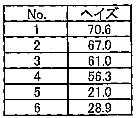
この結果から、 パターンが不連続な形状を示す場合において、 ヘイズ値が高い ことがわかり、 ヘイズとパターン形状に相関関係があることがわかる。 This result indicates that the haze value is high when the pattern shows a discontinuous shape, and that there is a correlation between the haze and the pattern shape.
②屈折率差の影響確認 ② Check the effect of the difference in refractive index
上記①の凹凸形状による効果の確認で使用した基板上に液晶材料 (屈折率 A liquid crystal material (refractive index
1.45) を滴下し、 パターンが形成されていない透明基板を重ねて上記と同様にへ ィズ測定を実施した。 測定結果を下記表 4に示す。 1.45) was dropped, and a transparent substrate on which no pattern was formed was overlapped, and a haze measurement was performed in the same manner as above. The measurement results are shown in Table 4 below.
[表 4 ] [Table 4]

上記表 3の結果から、 上記①凹凸形状による効果の確認で良好であつたヘイズ 値が低下していることがわかる。 これは、 屈折率差の影響を示しているもので、 上記①凹凸形状による効果の確認では、 オーバーコート材 (屈折率 1.5) と空気
(屈折率 1 .0) の屈折率差が 0.5 と大きいためにヘイズ値が良好であつたと推定 できる。 From the results in Table 3 above, it can be seen that the haze value, which was good in the confirmation of the effect of the above-mentioned uneven shape, was reduced. This indicates the effect of the difference in the refractive index. In the above ①, the effect of the uneven shape was confirmed, and the overcoat material (refractive index 1.5) and air Since the refractive index difference of (refractive index 1.0) is as large as 0.5, it can be estimated that the haze value was good.
③擬似パネルによる屈折率差の確認 ' 更に、 現状のディスプレイと同様の構成を想定し、 上記①凹凸形状による効果 の確認で用いた基板にスパッタリングにより ITO膜 ( 1 5 0 0 A、 屈折率 1.8) と、 スピンコートにより配向膜 (6 0 0 A、 屈折率 1.6) とを形成した。 この基 板に対して、 上記②屈折率差の影響確認と同様の方法で、 ヘイズ値を測定した。 測定結果を下記表 5に示す。 ③Confirmation of refractive index difference by simulated panel '' Furthermore, assuming the same configuration as the current display, the above-mentioned ①The ITO film (150 A, refractive index 1.8 ) And an alignment film (600 A, refractive index 1.6) was formed by spin coating. The haze value of this substrate was measured in the same manner as described above for confirming the effect of the difference in refractive index. Table 5 below shows the measurement results.
[表 5 ] [Table 5]

上記表 4および表 5の結果を比較すると、 ヘイズ値がほとんど変化が見られな い。 これは、 ITO膜、 配向膜ともにその膜厚が薄く、 屈折率差に影響を及ぼさな いことを示している。 When the results in Tables 4 and 5 are compared, the haze value hardly changes. This indicates that the thickness of both the ITO film and the alignment film is small, and does not affect the refractive index difference.
以上の結果より、 パターン形状と屈折率差が重要なフアクターであることがわ かった。 From the above results, it was found that the pattern shape and the refractive index difference are important factors.
次に、 透明基板として、 基板サイズ 300 X 400mm、 厚さ 0.7mm (コ一二ング 社製 1737材) を用いて、 洗剤洗浄■乾燥工程を行った。 Next, using a transparent substrate having a substrate size of 300 × 400 mm and a thickness of 0.7 mm (1737 manufactured by Koingen Co., Ltd.), a detergent washing and drying process was performed.
次に、定法の方法により、スパッタリングにより、 て膜を1 5 0 0 A成膜し、 ポジレジストを塗布し、 プレベータ ·露光 ·現像 ·エッチング ·剥離の工程を経 て、 ブラックマトリクス基板を形成した。 Next, a conventional method was used to form a film of 150 A by sputtering, apply a positive resist, and form a black matrix substrate through the steps of pre-beta, exposure, development, etching, and peeling. .
次に、 着色層の形成には以下に示す屈折率 1.5の着色感材を用いた。 Next, a colored photosensitive material having a refractive index of 1.5 shown below was used for forming a colored layer.
II感材 カラーモザイク CR 9 0 0 0 (富士フィルムアーチ製) II Sensitive Material Color Mosaic CR 9000 (Fuji Film Arch)
G感材 カラーモザイク CG 9 0 0 0 (富士フィルムアーチ製) G Sensitive Material Color Mosaic CG 900 (Fuji Film Arch)
B感材 カラーモザイク CB 9 0 0 0 (富士フィルムアーチ製) B Sensitive Material Color Mosaic CB9000 0 (Fuji Film Arch)
(Rストライプパターンの形成) (Formation of R stripe pattern)
上記のブラックマトリクス基板に対して、 R感材をスピンナ一により塗布 (620
r p ms 1 0秒保持) し、 プリベータ 8 0 °C、 3分で乾燥した後、 図 2 4に示す 繰り返しパターンを有するマスクを用い、 1 0 O m j Z c m2で露光、 現像 (専 用現像液で 7 0秒) 、 ポス トベータ (230°C、 3 0分) を行い、 反射部に凹凸部 を有するストライプパターンを形成した。 Apply R sensitive material to the above black matrix substrate with a spinner (620 rpm s 1 0 s hold), and dried over pre-beta 8 0 ° C, 3 minutes, using a mask having a repeating pattern shown in FIG. 2 4, 1 0 O mj Z cm 2 at exposure, development (developing dedicated The solution was subjected to a post-beta (230 ° C, 30 minutes) with a liquid for 70 seconds, and a stripe pattern having an uneven portion in the reflection portion was formed.
このパターンをレーザー顕微鏡にて観察し、 凹部を半球状として透過部の膜厚 力 ら差し引いて反射部の平均膜厚を算出した。 透過部の膜厚は、 2.0 mであり、 反射部の平均膜厚は、 Ι.Ο μ πιであった。 This pattern was observed with a laser microscope, and the average film thickness of the reflecting portion was calculated by subtracting the thickness of the transmitting portion from the film thickness of the transmitting portion, with the concave portion being a hemisphere. The thickness of the transmitting portion was 2.0 m, and the average thickness of the reflecting portion was Ι.Ομπι.
(Gストライプパターンの形成) (Formation of G stripe pattern)
塗布条件として 560 r p m、現像時間 1 3 0秒以外は Rストライプ形成と同様 に行った。透過部の膜厚は 2.0 mであり、反射部の平均膜厚は、 1 .0 ^ mであつ た。 Except for the application conditions of 560 rpm and a development time of 130 seconds, the same procedure as that for forming the R stripe was performed. The thickness of the transmitting part was 2.0 m, and the average thickness of the reflecting part was 1.0 ^ m.
(Bストライプパターンの形成) (Formation of B stripe pattern)
塗布条件として 690 r p m 現像時間 65秒以外は Rストライプ形成と同様に 行った。透過部の膜厚は 2.0 mであり、反射部の平均膜厚は、 1 .0 mであった。 Coating conditions were the same as those for R stripe formation except for 690 rpm development time of 65 seconds. The thickness of the transmitting part was 2.0 m, and the average thickness of the reflecting part was 1.0 m.
(光路差調整層の形成) (Formation of optical path difference adjustment layer)
光路差調整層としてポリイミド樹脂(フォトニース UR-4144 東レネ土製 屈折 率 1.6) をスピンナー (1000 r p m、 1 0秒保持) で塗布し、 プリベータとして 9 0 °C、 3分で乾燥した後、 図 2 5に示す繰り返しパターンを有するマスクを用 い、 300m j / c m 2で露光、現像(専用現像液 6 0秒)、ボストベータ(2 3 0 °C、 3 0分) を行い、 反射部のみに光路差調整層を形成した。 これにより、 光路差調 整層と着色層との屈折率差は 0.1に調整され、 また反射部の膜厚は 4.3 /z m、 透 過部の膜厚は 2.0 mに調整できた。 A polyimide resin (Photo Nice UR-4144, made by Toray Rene Earth Co., Ltd., refractive index: 1.6) is applied as an optical path difference adjustment layer using a spinner (1000 rpm, holding for 10 seconds), and dried at 90 ° C and 3 minutes as a pre-beta. There use a mask having a repeating pattern shown in 2 5, exposed at 300 meters j / cm 2, development (dedicated developer 6 0 seconds), the Bosutobeta (2 3 0 ° C, 3 0 minutes), only in the reflective portion An optical path difference adjusting layer was formed. As a result, the refractive index difference between the optical path difference adjusting layer and the coloring layer was adjusted to 0.1, the thickness of the reflecting portion was adjusted to 4.3 / zm, and the thickness of the transmitting portion was adjusted to 2.0 m.
次に、 スパッタリングにより、 ITO膜を 1500 A形成し、 柱状スぺーサ一形成 用材料 (JSR製ォプトマ一) をポス トべーク後 2 . 3 /z mになるように塗布し、 反射部のブラックマトリクスに対応する部分に柱状スぺーサーを形成するマスク を使用し、 反射部に柱状スぺーサーを形成した。 背面電極基板とカラーフィルタ 基板に対して、 配向膜を塗布 'ラビングした後、 外周シール部にシール材を塗布 し、 重ね合わせて、 ネマチック液晶を液晶物質として封入し、 封入口を封止し偏 向板および位相差板を組み入れて半透過カラー液晶表示装置を組み立てた。
上記背面側電極基板に設けられた透明電極層とカラーフィルタ基板に設けられ た透明電極基板の間に電圧を印加して画面を表示したところ、 バックライトから の入射光で十分明るいカラー画像の表示画面を認識することができた。 同じく、 背面側電極基板に設けられた金属反射電極とカラーフィルタ基板に設けられた透 明電極基板の間に電圧を印加して画面を表示したところ、 反射用入射光により、 その画面は透過光表示と比較してカラーフィルタを 2回通過しているにもかかわ らず、 透過光と同様に十分明るレ、鮮明な表示画面であった。 Next, an ITO film was formed to a thickness of 1500 A by sputtering, and a columnar spacer forming material (JSR Optoma) was applied to a thickness of 2.3 / zm after the postbaking, and the reflection portion was formed. Using a mask that forms a columnar spacer in the area corresponding to the black matrix, a columnar spacer was formed in the reflective area. After applying an alignment film to the back electrode substrate and the color filter substrate, rubbing, applying a sealing material to the outer peripheral seal part, superimposing, filling the nematic liquid crystal as a liquid crystal substance, sealing the filling port, and sealing A transflective color liquid crystal display device was assembled by incorporating a facing plate and a retardation plate. When a voltage was applied between the transparent electrode layer provided on the back side electrode substrate and the transparent electrode substrate provided on the color filter substrate to display a screen, a sufficiently bright color image was displayed with incident light from the backlight. I was able to recognize the screen. Similarly, when a screen was displayed by applying a voltage between the metal reflective electrode provided on the rear electrode substrate and the transparent electrode substrate provided on the color filter substrate, the screen was transmitted by the incident light for reflection. Despite passing through the color filter twice as compared to the display, the display screen was sufficiently bright and sharp as the transmitted light.
(実施例 4 ) (Example 4)
以下の光路差調整層の形成以外は、 実施例 3と同じ工程により作成した。 Except for the formation of the optical path difference adjusting layer described below, it was formed by the same steps as in Example 3.
光路差調整層としてポリイミド樹脂(フォトニース UR-4144 東レネ土製 屈折 率 1.6) をスピン ^ "一 (1000 r p m、 1 0秒保持) で塗布し、 プリべークとして 9 0 °C、 3分で乾燥した後、 図 2 6に示す繰り返しパターンを有するマスクを用 レ、、 300m j Z c m 2で露光、現像(専用現像液 6 0秒)、ボストベータ(2 3 0 °C、 3 0分) を行い、 反射部のみに表面に凹凸を有する光路差調整層を形成した。 こ れにより、 光路差調整層と着色層との屈折率差は 0.1に調整され、 光路差調整層 と液晶層 (屈折率 1.45) との屈折率差は 0.15に調整され、 また反射部の膜厚は 実施例 3と同様に 4.3 μ m、 透過部の膜厚は 2.0 mに調整できた。 A polyimide resin (Photo Nice UR-4144, made by Toray Rindo Earth Co., Ltd., refractive index: 1.6) is applied as an optical path difference adjustment layer by spin ^ "one (1000 rpm, 10 seconds hold), and prebaked at 90 ° C for 3 minutes. after in the drying, exposed in use les ,, 300 meters j Z cm 2 a mask having a repeating pattern shown in FIG. 2 6, developing (dedicated developer 6 0 seconds), Bosutobeta (2 3 0 ° C, 3 0 minutes) Then, an optical path difference adjusting layer having an uneven surface was formed only in the reflecting portion, whereby the refractive index difference between the optical path difference adjusting layer and the colored layer was adjusted to 0.1, and the optical path difference adjusting layer and the liquid crystal layer ( The refractive index difference from the refractive index of 1.45) was adjusted to 0.15, and the film thickness of the reflection part was 4.3 μm and the film thickness of the transmission part was 2.0 m, as in Example 3.
実施例 3と同様に半透過カラー液晶表示装置として観察したところ、 反射モー ドでは更に視覚依存性が改善されていた。 Observation as a transflective color liquid crystal display device as in Example 3 revealed that the visual dependency was further improved in the reflection mode.
(実施例 5 ) (Example 5)
以下の光路差調整層の形成以外は、 実施例 3と同じ工程により作成した。 Except for the formation of the optical path difference adjusting layer described below, it was formed by the same steps as in Example 3.
光路差調整層として低屈折材料 (ォプスター JN JSR社製 屈折率 1.4) をス ピンナー (1000 r p m、 30秒保持) で塗布し、 プリベータとして 9 0 °C、 3分 で乾燥した後、 図 2 4に示す繰り返しパターンを有するマスクを用い、 300m j Z c m 2で露光、 現像 (専用現像液 6 0秒) 、 ポス トベータ (2 3 0 °C、 3 0分) を行い、 反射部のみに光路差調整層を形成した。 これにより、 光路差調整層と着 色層との屈折率差は 0.1に調整され、 また反射部の膜厚は 4.3 m、 透過部の膜 厚は 2.0 /z mに調整できた。 A low refractive material (refractive index 1.4, manufactured by Opstar JN JSR) was applied as an optical path difference adjusting layer with a spinner (1000 rpm, holding for 30 seconds) and dried as a pre-beta at 90 ° C for 3 minutes. using a mask having a repeating pattern shown in, exposure at 300 meters j Z cm 2, development (dedicated developer 6 0 seconds), the post Tobeta (2 3 0 ° C, 3 0 minutes), an optical path difference only in the reflective portion An adjustment layer was formed. As a result, the refractive index difference between the optical path difference adjusting layer and the coloring layer was adjusted to 0.1, the thickness of the reflecting portion was adjusted to 4.3 m, and the thickness of the transmitting portion was adjusted to 2.0 / zm.
実施例 3と同様に半透過カラー液晶表示装置として観察したところ、 同様の効
果が得られた。 When observed as a transflective color liquid crystal display device in the same manner as in Example 3, the same effect was obtained. The fruit was obtained.
(実施例 6 ) (Example 6)
以下の光路差調整層の形成以外は、 実施例 3と同じ工程により作成した。 Except for the formation of the optical path difference adjusting layer described below, it was formed by the same steps as in Example 3.
光路差調整層として低屈折材料 (ォプスター JN JSR社製 屈折率 1.4) をス ピンナー (1000 r p m、 30秒保持) で塗布し、 プリベータとして 9 0 °C、 3分 で乾燥した後、 図 2 5に示す繰り返しパターンを有するマスクを用い、 300m j c m2で露光、 現像 (専用現像液 6 0秒) 、 ポストべーク (2 3 0 °C、 3 0分) を行い、反射部のみに表面に凹凸を有する光路差調整層を形成した。これにより、 光路差調整層と着色層との屈折率差は 0.1に調整され、光路差調整層と液晶層(屈 折率 1.45) との屈折率差は 0.05に調整され、 また反射部の膜厚は実施例 3と同 様に 4.3 m、 透過部の膜厚は 2.0 /x mに調整できた。 A low refraction material (refractive index: 1.4, manufactured by Opstar JN JSR) was applied as an optical path difference adjusting layer using a spinner (holding at 1000 rpm for 30 seconds) and dried as a pre-beta at 90 ° C for 3 minutes. Exposure at 300 mjcm 2 using a mask with the repetitive pattern shown in (1), development (dedicated developer 60 seconds) and post bake (230 ° C, 30 minutes) An optical path difference adjusting layer having irregularities was formed. As a result, the refractive index difference between the optical path difference adjusting layer and the coloring layer is adjusted to 0.1, the refractive index difference between the optical path difference adjusting layer and the liquid crystal layer (refractive index: 1.45) is adjusted to 0.05, The thickness could be adjusted to 4.3 m as in Example 3, and the thickness of the transmission part could be adjusted to 2.0 / xm.
実施例 3と同様に半透過カラー液晶表示装置として観察したところ、 反射モー ドでは実施例 3と比べ若干、 視覚依存性が改善されていた。 When observed as a transflective color liquid crystal display device in the same manner as in Example 3, the visual dependency was slightly improved in the reflection mode as compared with Example 3.
(実施例 7 ) (Example 7)
以下の光路差調整層の形成以外は、 実施例 3と同じ工程により作成した。 Except for the formation of the optical path difference adjusting layer described below, it was formed by the same steps as in Example 3.
光路差調整層としてオーバーコート材(ザ 'インクテック社製 IT-MP 屈折率 1.50) に酸ィ匕チタン微粒子を分散させた材料をスピンナー (1000 r p m、 1 0秒 保持) で塗布し、 プリベータとして 9 0 °C、 3分で乾燥した後、 図 2 5に示す繰 り返しパターンを有するマスクを用い、 300m j Z c m 2で露光、 現像 (専用現像 液 6 0秒) 、 ポストベータ (2 3 0 °C、 3 0分) を行い、 反射部のみに光路差調 整層を形成した。酸化チタン微粒子を分散したオーバーコート材の屈折率は、 1.65 であった。光路差調整層と着色層との屈折率差は 0.15に調整できた。 また反射部 の膜厚は 4.3 μ m、 透過部の膜厚は 2.0 μ: mに調整できた。 As an optical path difference adjustment layer, a material in which fine particles of titanium oxide are dispersed in an overcoat material (IT-MP refractive index: 1.50 manufactured by Inktec Co., Ltd.) is applied with a spinner (1000 rpm, 10 seconds hold), and used as a pre-beta. 9 0 ° C, dried at 3 minutes, using a mask having a Repetitive return pattern shown in FIG. 2 5, 300 meters j Z cm 2 at exposure, development (dedicated developer 6 0 seconds), post-beta (2 3 (0 ° C, 30 minutes) to form an optical path difference adjusting layer only on the reflection part. The refractive index of the overcoat material in which the titanium oxide fine particles were dispersed was 1.65. The refractive index difference between the optical path difference adjusting layer and the colored layer could be adjusted to 0.15. The thickness of the reflective part was 4.3 μm, and the thickness of the transmissive part was 2.0 μm.
実施例 3と同様に半透過カラー液晶表示装置として観察したところ、 反射モー ドでは更に視覚依存性が改善されていた。 Observation as a transflective color liquid crystal display device as in Example 3 revealed that the visual dependency was further improved in the reflection mode.
(実施例 8 ) (Example 8)
以下の光路差調整層の形成以外は、 実施例 3と同じ工程により作成した。 Except for the formation of the optical path difference adjusting layer described below, it was formed by the same steps as in Example 3.
光路差調整層としてオーバーコート材 (ザ'インクテック社製 IT-MP 屈折率 1.50) に酸化チタン微粒子を分散させた材料をスピンナー (1000 r TD in、 1 0秒
保持) で塗布し、 プリベータとして 9 0 °C、 3分で乾燥した後、 図 2 6に示す繰 り返しパターンを有するマスクを用い、 300m j Z c m 2で露光、 現像 (専用現像 液 6 0秒) 、 ポス トベータ (2 3 0 °C、 3 0分) を行い、 反射部のみに表面に凹 凸を有する光路差調整層を形成した。 酸化チタン微粒子を分散したオーバーコー ト材の屈折率は、 1 .65であった。 光路差調整層と液晶層 (屈折率 1.45) との屈 折率差は 0.20に調整され、 光路差調整層と着色層との屈折率差は 0.15に調整で きた。 また反射部の膜厚は実施例 3と同様に 4.3/z ;m、透過部の膜厚は 2.0 ;z mに 調整できた。 As an optical path difference adjusting layer, a material in which titanium oxide fine particles are dispersed in an overcoat material (IT-MP refractive index: 1.50 manufactured by The Inktec Co., Ltd.) is used as a spinner (1000 r TD in, 10 seconds) It was applied at a holding), dried over 9 0 ° C, 3 minutes as pre-beta, using a mask having a Repetitive return pattern shown in FIG. 2 6, 300m j Z cm 2 at exposure, development (dedicated developer 6 0 Seconds) and a post beta (230 ° C, 30 minutes) were performed to form an optical path difference adjustment layer having a concave / convex surface only in the reflective part. The refractive index of the overcoat material in which the titanium oxide fine particles were dispersed was 1.65. The refractive index difference between the optical path difference adjusting layer and the liquid crystal layer (refractive index: 1.45) was adjusted to 0.20, and the refractive index difference between the optical path difference adjusting layer and the coloring layer was adjusted to 0.15. Further, the film thickness of the reflection part could be adjusted to 4.3 / z; m and the film thickness of the transmission part could be adjusted to 2.0; zm, as in Example 3.
実施例 3と同様に半透過力ラ一液晶表示装置として観察したところ、 反射モー ドでは更に視覚依存性が改善されていた。 Observation as a transflective liquid crystal display device in the same manner as in Example 3 revealed that the visual dependency was further improved in the reflection mode.
(比較例 3 ) (Comparative Example 3)
以下の光路差調整層の形成材料以外は、 実施例 3と同じ工程により作成した。 光路調整材料としてオーバーコート材(ザ'インクテック社製 IT-MP 屈折率 1.50) 使用した。 光路差調整層と着色層との屈折率差は 0であり、 光路差調整層 と液晶層との屈折率差は 0.05であつた。 Except for the following materials for forming the optical path difference adjusting layer, the optical path difference adjusting layer was formed in the same process as in Example 3. As an optical path adjusting material, an overcoat material (IT-MP manufactured by The Inktec Co., Ltd., refractive index: 1.50) was used. The refractive index difference between the optical path difference adjusting layer and the colored layer was 0, and the refractive index difference between the optical path difference adjusting layer and the liquid crystal layer was 0.05.
実施例 3と同様に半透過カラー液晶表示装置として観察したところ、 反射モー ドでは、 透過モードに比べ明るさが劣っていた。 Observation as a transflective color liquid crystal display device as in Example 3 revealed that the brightness was inferior in the reflective mode as compared to the transmissive mode.
(比較例 4 ) (Comparative Example 4)
以下の光路差調整層の形成材料以外は、 実施例 4と同じ工程により作成した。 光路調整材料としてオーバーコート材 (ザ 'インクテック社製 IT-MP 屈折率 1.50) 使用した。 光路差調整層と着色層との屈折率差は 0であり、 光路差調整層 と液晶層との屈折率差は 0.05であつた。 Except for the following materials for forming the optical path difference adjusting layer, the same steps as in Example 4 were used. An overcoat material (IT-MP manufactured by Inktec Co., Ltd., refractive index: 1.50) was used as an optical path adjusting material. The refractive index difference between the optical path difference adjusting layer and the colored layer was 0, and the refractive index difference between the optical path difference adjusting layer and the liquid crystal layer was 0.05.
実施例 3と同様に半透過カラー液晶表示装置として観察したところ、 反射モー ドでは、 透過モードに比べ明るさが劣っていた。
Observation as a transflective color liquid crystal display device as in Example 3 revealed that the brightness was inferior in the reflective mode as compared to the transmissive mode.
Claims
1 . 透明基板と、 前記透明基板上に透明膜がパターン状に形成されてなる透明 膜パターン層と、 前記透明膜パターン層を覆うように形成された着色層とが積層 されてなる透明膜パターン領域を有することを特徴とする半透過半反射型液晶表 示装置用カラーフィルタ。 1. A transparent film pattern formed by laminating a transparent substrate, a transparent film pattern layer in which a transparent film is formed in a pattern on the transparent substrate, and a coloring layer formed to cover the transparent film pattern layer A color filter for a transflective liquid crystal display device having a region.
2 . 前記透明膜パターン領域を反射光用領域に用い、 前記透明基板と、 前記透 明基板上に形成された着色層とを有する着色層領域を透過光用領域に用いること を特徴とする請求項 1に記載の半透過半反射型液晶表示装置用カラーフィルタ。 2. The transparent film pattern region is used as a reflected light region, and a colored layer region having the transparent substrate and a colored layer formed on the transparent substrate is used as a transmitted light region. Item 2. A color filter for a transflective liquid crystal display device according to item 1.
3 . 前記透明膜パターン領域を透過光用領域に用い、 前記透明基板と、 前記透 明基板上に透明膜が均一に形成されてなる透明膜均一層と、 前記透明膜均一層上 に形成された着色層とが積層されてなる透明膜均一領域を反射光用領域に用いる ことを特徴とする請求項 1に記載の半透過半反射型液晶表示装置用カラーフィル タ。 3. The transparent film pattern region is used as a region for transmitted light, the transparent substrate, a transparent film uniform layer in which a transparent film is uniformly formed on the transparent substrate, and a transparent film uniform layer formed on the transparent film uniform layer. 2. The color filter for a transflective liquid crystal display device according to claim 1, wherein a uniform region of the transparent film in which the colored layer is laminated is used as a region for reflected light.
4 .前記透明膜パタ一ン領域内における透明膜が形成される領域の面積比が (透 明膜形成面積ノ透明膜パターン領域面積) = 0 . 3〜 0 . 5の範囲内であることを 特徴とする請求項 3に記載の半透過半反射型液晶表示装置用力ラーフィルタ。 4. The area ratio of the area where the transparent film is formed in the transparent film pattern area is (transparent film forming area / transparent film pattern area area) = 0.3 to 0.5. 4. The power filter for a transflective liquid crystal display device according to claim 3, wherein:
5 .前記透明膜パターン層および前記透明膜均一層を形成する透明膜の膜厚が、 前記着色層が前記着色層のみで透過光用領域に用いられる場合の着色層の膜厚を 1とした場合に 0 . 5〜 3 . 0の範囲内の膜厚とすることを特徴とする請求項 4に 記載の半透過半反射型液晶表示装置用カラーフィルタ。 5. The thickness of the transparent film that forms the transparent film pattern layer and the transparent film uniform layer is set to 1 when the colored layer is used only in the colored layer and used in the transmitted light region. 5. The color filter for a transflective liquid crystal display device according to claim 4, wherein the film thickness is in the range of 0.5 to 3.0.
6 . 前記透明膜パターン層は、 透明膜が島状に形成されてなるパターンを有す ることを特徴とする請求項 1から請求項 5までのいずれかの請求項に記載の半透 過半反射型液晶表示装置用カラーフィルタ。 6. The transflective semi-reflection according to any one of claims 1 to 5, wherein the transparent film pattern layer has a pattern in which a transparent film is formed in an island shape. Color filter for liquid crystal display devices.
7 . 前記透明膜パターン層が、 透明膜に孔部がパターン状に形成されてなるパ タ一ンを有することを特徴とする請求項 1から請求項 5までのレ、ずれかの請求項 に記載の半透過半反射型液晶表示装置用力ラーフイノレタ。 7. The transparent film pattern layer according to any one of claims 1 to 5, wherein the transparent film has a pattern in which holes are formed in a pattern in the transparent film. 12. A power transmission device for a transflective liquid crystal display device according to the above.
8 . 前記透明膜パターン層の島状に形成されている部分または孔部が、 円状に 形成されていることを特徴とする請求項 1から請求項 7までのいずれかの請求項
に記載の半透過半反射型液晶表示装置用カラー: 8. The island portion or the hole portion of the transparent film pattern layer is formed in a circular shape. Color for transflective liquid crystal display device described in:
9 . 前記透明膜パターン層、 または前記透明膜パターン層および前記透明膜均 一層を形成する透明膜の膜厚が、 0 . 5〜3 . 5 μ πιであることを特徴とする請求 項 1から請求項 8までのいずれかの請求項に記載の半透過半反射型液晶表示装置 用カラーフィルタ。 9. The film thickness of the transparent film pattern layer or the transparent film forming the transparent film pattern layer and the transparent film uniform layer is 0.5 to 3.5 μπι. 9. A color filter for a transflective liquid crystal display device according to claim 8.
1 0 . 前記透明膜の波長 3 8 0 n m〜7 8 0 n mにおける分光透過率が 8 5 % 以上であることを特徴とする請求項 1から請求項 9までのいずれかの請求項に記 载の半透過半反射型液晶表示装置用カラーフィルタ。 10. The method according to any one of claims 1 to 9, wherein the transparent film has a spectral transmittance at a wavelength of 380 nm to 780 nm of 85% or more. Color filter for transflective liquid crystal display devices.
1 1 . 請求項 1から請求項 1 0までのいずれかの請求項に記載の半透過半反射 型液晶表示装置用カラーフィルタを有することを特徴とする半透過半反射型液晶 11. A transflective liquid crystal comprising the color filter for a transflective liquid crystal display device according to any one of claims 1 to 10.
1 2 . 透明基板と、 前記透明基板上に形成された反射光用着色層および透過光 用着色層とを有する半透過型力ラ一液晶表示装置用カラーフィルタであって、 前記反射光用着色層は、 その液晶層側表面に凹凸が形成され、 かつ平均膜厚が 前記透過光用着色層の膜厚より薄くなるように形成され、 12. A transflective color filter for a liquid crystal display device, comprising: a transparent substrate; and a colored layer for reflected light and a colored layer for transmitted light formed on the transparent substrate, wherein the color filter for reflected light is provided. The layer is formed such that irregularities are formed on the liquid crystal layer side surface, and the average film thickness is smaller than the film thickness of the transmitted light colored layer.
前記反射光用着色層と、 前記反射光用着色層の凹凸が形成されている側の表面 に接触する層との屈折率差が 0 . 1以上であることを特徴とする半透過型カラー 液晶表示装置用カラーフィルタ。 ' A transflective color liquid crystal, wherein a difference in refractive index between the colored layer for reflected light and a layer that comes into contact with the surface of the colored layer for reflected light on which the unevenness is formed is 0.1 or more. Color filters for display devices. '
1 3 . 前記反射光用着色層と、 前記反射光用着色層の囬凸が形成されている側 の表面に接触する層との屈折率差が 0 . 1以上となるように、 前記反射光用着色 層に屈折率を高める屈折率増加剤が含有されていることを特徴とする請求項 1 2 に記載の半透過型力ラ一液晶表示装置用カラーフィルタ。 13. The reflected light so that the difference in refractive index between the colored layer for reflected light and the layer in contact with the surface of the colored layer for reflected light on which the convexity is formed is 0.1 or more. The color filter for a transflective liquid crystal display device according to claim 12, wherein the coloring layer for use contains a refractive index increasing agent for increasing the refractive index.
1 4 . 前記反射光用着色層表面の凹凸が、 透過光用着色層と同じ膜厚で形成さ れた反射光用着色層表面に曲面で構成される複数の凹部を形成してなるものであ ることを特徴とする請求項 1 2または請求項 1 3に記載の半透過型力ラー液晶表 示装置用カラーフィルタ。 14. The unevenness on the surface of the colored layer for reflected light is obtained by forming a plurality of concave portions formed of curved surfaces on the surface of the colored layer for reflected light formed with the same thickness as the colored layer for transmitted light. 14. The color filter for a transflective liquid crystal display device according to claim 12, wherein the color filter is used.
1 5 . 前記反射光用着色層の凹凸が形成されている側の表面に接触する層が、 反射光領域と透過光領域との光路差を調整するための光路差調整層であることを 特徴とする請求項 1 2から請求項 1 4までのいずれかの請求項に記載の半透過型
力ラ一液晶表示装置用カラーフィルタ。 15. The layer that comes into contact with the surface of the colored layer for reflected light on which the unevenness is formed is an optical path difference adjusting layer for adjusting the optical path difference between the reflected light region and the transmitted light region. The transflective type according to any one of claims 12 to 14 Color filters for liquid crystal display devices.
1 6 . 透明基板と、 前記透明基板上に形成された反射光用着色層および透過光 用着色層とを有する半透過型力ラ一液晶表示装置用カラーフィルタであって、 前記反射光用着色層は、 その液晶層側表面に凹凸が形成され、 かつ平均膜厚が 前記透過光用着色層の膜厚より薄くなるように形成され、 16. A transflective color filter for a liquid crystal display device comprising: a transparent substrate; and a colored layer for reflected light and a colored layer for transmitted light formed on the transparent substrate, wherein the color filter for reflected light is used. The layer is formed such that irregularities are formed on the liquid crystal layer side surface, and the average film thickness is smaller than the film thickness of the transmitted light colored layer.
前記反射光用着色層の凹凸が形成されている側の表面には、 反射光領域と透過 光領域との光路差を調整するための光路差調整層が形成され、 An optical path difference adjustment layer for adjusting the optical path difference between the reflected light area and the transmitted light area is formed on the surface of the reflected light colored layer on which the unevenness is formed,
前記反射光用着色層と、 前記光路差調整層との屈折率差が 0 . 1以上となるよ うに、 前記光路差調整層に屈折率を高める屈折率増加剤が含有されていることを 特徴とする半透過型力ラ一液晶表示装置用カラーフィルタ。 The optical path difference adjusting layer contains a refractive index increasing agent that increases the refractive index such that the refractive index difference between the reflected light colored layer and the optical path difference adjusting layer is 0.1 or more. A color filter for a liquid crystal display device.
1 7 . 前記反射光用着色層表面の 凸が、 透過光用着色層と同じ膜厚で形成さ れた反射光用着色層表面に曲面で構成される複数の凹部を形成してなるものであ ることを特徴とする請求項 1 6に記載の半透過型力ラ一液晶表示装置用カラーフ イノレタ。 17. The convexities on the surface of the colored layer for reflected light are formed by forming a plurality of concave portions having curved surfaces on the surface of the colored layer for reflected light, which is formed with the same thickness as the colored layer for transmitted light. 17. The color fineta for a transflective liquid crystal display device according to claim 16, wherein:
1 8 . 前記光路差調整層は、 その液晶層側表面に凹凸が形成されており、 前記 光路差調整層と、 前記光路差調整層の凹凸が形成されている側の表面に接触する 層との屈折率差が 0 . 1以上であることを特徴とする請求項 1 6または請求項 1 7に記載の半透過型力ラ一液晶表示装置用カラーフィルタ。 18. The optical path difference adjusting layer has irregularities formed on the surface of the liquid crystal layer side, and the optical path difference adjusting layer and a layer that contacts the surface of the optical path difference adjusting layer on which the irregularities are formed. 18. The color filter for a transflective liquid crystal display device according to claim 16, wherein the refractive index difference of the liquid crystal display device is 0.1 or more.
1 9 . 前記光路差調整層表面の凹凸が、 光路差調整層表面に曲面で構成される 複数の囬部を形成してなるものであることを特徴とする請求項 1 8に記載の半透 過型力ラ一液晶表示装置用カラーフィルタ。 19. The semi-transparent film according to claim 18, wherein the irregularities on the surface of the optical path difference adjustment layer are formed by forming a plurality of curved portions on the surface of the optical path difference adjustment layer. Color filter for liquid crystal display device.
2 0 . 透明基板と、 前記透明基板上に形成された反射光用着色層および透過光 用着色層とを有する半透過型力ラ一液晶表示装置用カラーフィルタであって、 前記反射光用着色層は、 その液晶層側表面に凹凸が形成され、 かつ平均膜厚が 前記透過光用着色層の膜厚より薄くなるように形成され、 20. A transflective color filter for a liquid crystal display device, comprising: a transparent substrate; and a colored layer for reflected light and a colored layer for transmitted light formed on the transparent substrate. The layer is formed such that irregularities are formed on the liquid crystal layer side surface, and the average film thickness is smaller than the film thickness of the transmitted light colored layer.
前記反射光用着色層の凹凸が形成されている側の表面には、 反射光領域と透過 光領域との光路差を調整するための光路差調整層が形成され、 前記光路差調整層 の液晶層側表面にも [Ϊ]凸が形成されており、 An optical path difference adjusting layer for adjusting the optical path difference between the reflected light area and the transmitted light area is formed on the surface of the reflected light colored layer on which the unevenness is formed, and the liquid crystal of the optical path difference adjusting layer [Ϊ] convexity is also formed on the layer side surface,
前記光路差調整層の凹凸が形成されている側の表面には、 光路差調整層表面を
平坦にするため光路差調整層用平坦化層が形成されており、 On the surface of the optical path difference adjustment layer on which the unevenness is formed, the surface of the optical path difference adjustment layer is A flattening layer for an optical path difference adjustment layer is formed to make it flat,
前記光路差調整層および前記光路差調整層用平坦化層の屈折率差が 0 . 1以上 であることを特徴とする半透過型力ラ一液晶表示装置用カラーフィルタ。 A color filter for a transflective liquid crystal display device, wherein the refractive index difference between the optical path difference adjusting layer and the flattening layer for the optical path difference adjusting layer is 0.1 or more.
2 1 . 前記光路差調整層および前記光路差調整層用平坦化層の屈折率差が 0 · 1以上となるように、 前記光路差調整層用平坦化層に屈折率を高める屈折率増加 剤が含有されていることを特徴とする請求項 2 0に記載の半透過型力ラ一液晶表 示装置用カラーフィルタ。 21. A refractive index increasing agent for increasing the refractive index of the planarization layer for the optical path difference adjustment layer so that the refractive index difference between the optical path difference adjustment layer and the planarization layer for the optical path difference adjustment layer becomes 0.1 or more. 22. The color filter for a transflective liquid crystal display device according to claim 20, further comprising:
2 2 . 前記光路差調整層および前記反射光用着色層の屈折率差が 0 . 1以上と なるように、 前記反射光用着色層に屈折率を高める屈折率増加剤が含有されてい ることを特徴とする請求項 2 0または請求項 2 1に記載の半透過型力ラ一液晶表 示装置用カラーフィルタ。 22. The colored layer for reflected light contains a refractive index increasing agent for increasing the refractive index such that the difference in refractive index between the optical path difference adjusting layer and the colored layer for reflected light is 0.1 or more. 22. The color filter for a transflective liquid crystal display device according to claim 20, wherein the color filter is a liquid crystal display device.
2 3 . 前記反射光用着色層表面の (Κ!凸が、 透過光用着色層と同じ膜厚で形成さ れた反射光用着色層表面に曲面で構成される複数の凹部を形成してなるものであ ることを特徴とする請求項 2 0から請求項 2 2までのいずれかの請求項に記載の 半透過型カラー液晶表示装置用カラーフィルタ。 23. A plurality of concave portions formed of curved surfaces are formed on the surface of the colored layer for reflected light in which the (Κ! Convex is formed with the same thickness as the colored layer for transmitted light. The color filter for a transflective color liquid crystal display device according to any one of claims 20 to 22, characterized in that:
2 4 . 前記光路差調整層表面の凹凸が、 光路差調整層表面に曲面で構成される 複数の凹部を形成してなるものであることを特徴とする請求項 2 0から請求項 2 3までのいずれかの請求項に記載の半透過型カラー液晶表示装置用カラーフィル タ。 24. The irregularities on the surface of the optical path difference adjustment layer are formed by forming a plurality of concave portions having curved surfaces on the surface of the optical path difference adjustment layer. The color filter for a transflective color liquid crystal display device according to claim 1.
2 5 . 透明基板と、 前記透明基板上に形成された反射光用着色層および透過光 用着色層を有する半透過型力ラ一液晶表示装置用カラーフィルタであって、 前記反射光用着色層は、 その平均膜厚が前記透過光用着色層の膜厚より薄くな るように少なくとも一つの除去部が形成され、 25. A transflective color filter for a liquid crystal display device having a transparent substrate and a colored layer for reflected light and a colored layer for transmitted light formed on the transparent substrate, wherein the colored layer for reflected light is provided. At least one removed portion is formed such that its average thickness is smaller than the thickness of the transmitted light colored layer,
前記反射光用着色層の液晶層側表面には、 反射光領域と透過光領域との光路差 を調整するための光路差調整層が形成され、 An optical path difference adjusting layer for adjusting an optical path difference between a reflected light region and a transmitted light region is formed on the liquid crystal layer side surface of the reflected light colored layer,
前記光路差調整層の液晶層側表面には凹凸が形成されており、 Irregularities are formed on the liquid crystal layer side surface of the optical path difference adjustment layer,
前記光路差調整層と、 前記光路差調整層の凹凸が形成されている側の表面に接 触する層との屈折率差が 0 . 1以上であることを特徴とする半透過型力ラ一液晶 表示装置用力ラ
A semi-transmissive power liner, wherein a difference in refractive index between the optical path difference adjusting layer and a layer in contact with the surface of the optical path difference adjusting layer on the side where the unevenness is formed is 0.1 or more. Liquid crystal display device
2 6 . 前記光路差調整層と、 前記光路差調整層の凹凸が形成されている側の表 面に接触する層との屈折率差が 0 . 1以上となるように、前記光路差調整層には、 屈折率を高める屈折率増力 B剤が含有されていることを特徴とする請求項 2 5に記 載の半透過型力ラ一液晶表示装置用カラーフィルタ。 26. The optical path difference adjusting layer such that a refractive index difference between the optical path difference adjusting layer and a layer that comes into contact with the surface of the optical path difference adjusting layer on which the unevenness is formed is 0.1 or more. 26. The color filter for a transflective liquid crystal display device according to claim 25, further comprising a refractive index enhancing agent B for increasing a refractive index.
2 7 . 透明基板と、 前記透明基板上に形成された反射光用着色層および透過光 用着色層を有する半透過型力ラー液晶表示装置用カラーフィルタであって、 前記反射光用着色層は、 その平均膜厚が前記透過光用着色層の膜厚より薄くな るように少なくとも一つの除去部が形成され、 27. A color filter for a transflective liquid crystal display device having a transparent substrate, a colored layer for reflected light and a colored layer for transmitted light formed on the transparent substrate, wherein the colored layer for reflected light is At least one removed portion is formed such that its average thickness is smaller than the thickness of the transmitted light colored layer,
前記反射光用着色層の液晶層側表面には、 反射光領域と透過光領域との光路差 を調整するための光路差調整層が形成され、 An optical path difference adjusting layer for adjusting an optical path difference between a reflected light region and a transmitted light region is formed on the liquid crystal layer side surface of the reflected light colored layer,
前記光路差調整層の液晶層側表面には凹凸が形成されており、 Irregularities are formed on the liquid crystal layer side surface of the optical path difference adjustment layer,
前記光路差調整層の凹凸が形成されている側の表面には、 光路差調整層表面に 平坦性を得るために光路差調整雇用平坦化層が形成されており、 On the surface of the optical path difference adjustment layer where the unevenness is formed, an optical path difference adjustment employment flattening layer is formed to obtain flatness on the surface of the optical path difference adjustment layer,
前記光路差調整層と、 前記光路差調整層用平坦化層との屈折率差が 0 . 1以上 であることを特徴とする半透過型力ラ一液晶表示装置用カラーフィルタ。 A color filter for a transflective liquid crystal display device, wherein a refractive index difference between the optical path difference adjusting layer and the planarizing layer for the optical path difference adjusting layer is 0.1 or more.
2 8 . 前記光路差調整層と、 前記光路差調整層用平坦化層との屈折率差が 0 . 28. The difference in refractive index between the optical path difference adjusting layer and the planarizing layer for the optical path difference adjusting layer is 0.
1以上となるように、 前記光路差調整層用平坦化層に屈折率を高める屈折率增加 剤が含有されていることを特徴とする請求項 2 7に記載の半透過型カラー液晶表 示装置用カラーフィルタ。 28. The transflective color liquid crystal display device according to claim 27, wherein the flattening layer for an optical path difference adjusting layer contains a refractive index additive for increasing a refractive index so as to be 1 or more. For color filter.
2 9 . 前記光路差調整層表面の凹凸が、 光路差調整層表面に曲面で構成される 複数の凹部を形成してなるものであることを特徴とする請求項 2 5カゝら請求項 2 29. The unevenness on the surface of the optical path difference adjustment layer is formed by forming a plurality of concave portions having curved surfaces on the surface of the optical path difference adjustment layer.
8までのいずれかの請求項に記載の半透過型カラー液晶表示装置用カラーフィル タ。 9. The color filter for a transflective color liquid crystal display device according to claim 8, wherein
3 0 . 請求項 1 2から請求項 2 9までのいずれかの請求項に記載の半透過型力 ラ一液晶表示置用カラーフィルタを有することを特徴とする半透過型力ラ一液晶
30. A transflective liquid crystal comprising a color filter for a transflective liquid crystal display according to any one of claims 12 to 29.
Priority Applications (7)
| Application Number | Priority Date | Filing Date | Title |
|---|---|---|---|
| US10/513,968 US20050174511A1 (en) | 2002-05-09 | 2003-05-08 | Semi-transparent semi-reflective liquid crystal display device color filter |
| KR1020047017321A KR100890924B1 (en) | 2002-05-09 | 2003-05-08 | Semi-transparent semi-reflective liquid crystal display device color filter |
| US11/999,320 US7768599B2 (en) | 2002-05-09 | 2007-12-05 | Color filter for transflective type liquid crystal display |
| US12/401,824 US7948584B2 (en) | 2002-05-09 | 2009-03-11 | Color filter for transflective type liquid crystal display |
| US12/819,576 US7973887B2 (en) | 2002-05-09 | 2010-06-21 | Color filter for transflective type liquid crystal display |
| US12/819,603 US8130343B2 (en) | 2002-05-09 | 2010-06-21 | Color filter for transflective type liquid crystal display |
| US13/088,708 US8144292B2 (en) | 2002-05-09 | 2011-04-18 | Color filter for transflective type liquid crystal display |
Applications Claiming Priority (6)
| Application Number | Priority Date | Filing Date | Title |
|---|---|---|---|
| JP2002133979A JP4275351B2 (en) | 2002-05-09 | 2002-05-09 | Color filter for transflective liquid crystal display |
| JP2002-133979 | 2002-05-09 | ||
| JP2002382536A JP4255281B2 (en) | 2002-12-27 | 2002-12-27 | Color filter for transflective color LCD |
| JP2002382540A JP4245347B2 (en) | 2002-12-27 | 2002-12-27 | Color filter for transflective color LCD |
| JP2002-382540 | 2002-12-27 | ||
| JP2002-382536 | 2002-12-27 |
Related Child Applications (3)
| Application Number | Title | Priority Date | Filing Date |
|---|---|---|---|
| US10513968 A-371-Of-International | 2003-05-08 | ||
| US11/999,320 Division US7768599B2 (en) | 2002-05-09 | 2007-12-05 | Color filter for transflective type liquid crystal display |
| US12/401,824 Continuation US7948584B2 (en) | 2002-05-09 | 2009-03-11 | Color filter for transflective type liquid crystal display |
Publications (1)
| Publication Number | Publication Date |
|---|---|
| WO2003104861A1 true WO2003104861A1 (en) | 2003-12-18 |
Family
ID=29740535
Family Applications (1)
| Application Number | Title | Priority Date | Filing Date |
|---|---|---|---|
| PCT/JP2003/005785 WO2003104861A1 (en) | 2002-05-09 | 2003-05-08 | Semi-transparent semi-reflective liquid crystal display device color filter |
Country Status (5)
| Country | Link |
|---|---|
| US (6) | US20050174511A1 (en) |
| KR (2) | KR100890924B1 (en) |
| CN (2) | CN102096135B (en) |
| TW (1) | TWI254151B (en) |
| WO (1) | WO2003104861A1 (en) |
Cited By (1)
| Publication number | Priority date | Publication date | Assignee | Title |
|---|---|---|---|---|
| US8530115B2 (en) * | 2005-04-13 | 2013-09-10 | Samsung Display Co., Ltd. | Color filter array panel, liquid crystal display having the same, and manufacturing method thereof |
Families Citing this family (16)
| Publication number | Priority date | Publication date | Assignee | Title |
|---|---|---|---|---|
| KR100890924B1 (en) * | 2002-05-09 | 2009-04-03 | 다이니폰 인사츠 가부시키가이샤 | Semi-transparent semi-reflective liquid crystal display device color filter |
| KR100713891B1 (en) * | 2005-02-17 | 2007-05-04 | 비오이 하이디스 테크놀로지 주식회사 | Backlight unit for LCD |
| JP2008241726A (en) * | 2005-07-13 | 2008-10-09 | Sharp Corp | Substrate for liquid crystal display |
| WO2008010622A1 (en) * | 2006-07-19 | 2008-01-24 | Lg Electronics Inc. | Plasma display device |
| EP1890315A3 (en) * | 2006-08-18 | 2009-07-01 | LG Electronics Inc. | Filter and plasma display device thereof |
| EP2387081B1 (en) * | 2010-05-11 | 2015-09-30 | Samsung Electronics Co., Ltd. | Semiconductor light emitting device and method for fabricating the same |
| WO2012157601A1 (en) * | 2011-05-19 | 2012-11-22 | シャープ株式会社 | Liquid crystal display device |
| US20140233126A1 (en) * | 2011-05-31 | 2014-08-21 | Suzhou University | Reflective color filter |
| US8686433B2 (en) * | 2011-09-01 | 2014-04-01 | Rohm Co., Ltd. | Light emitting device and light emitting device package |
| US9209230B2 (en) | 2012-12-21 | 2015-12-08 | Samsung Electronics Co., Ltd | Optical films for reducing color shift and organic light-emitting display apparatuses employing the same |
| JP6286850B2 (en) * | 2013-03-29 | 2018-03-07 | 大日本印刷株式会社 | Color filter substrate for top emission type organic EL display device and top emission type organic EL display device |
| KR101616918B1 (en) | 2013-05-31 | 2016-04-29 | 제일모직주식회사 | Optical film for reducing color shift and organic light emitting display employing the same |
| KR102407761B1 (en) * | 2015-02-02 | 2022-06-13 | 삼성디스플레이 주식회사 | Liquid crystal display device |
| WO2018043517A1 (en) * | 2016-08-30 | 2018-03-08 | 富士フイルム株式会社 | Optical laminate |
| US10605421B2 (en) * | 2017-09-01 | 2020-03-31 | Robe Lighting S.R.O. | Dichroic patterning for subtractive color mixing |
| CN108227292A (en) * | 2018-02-11 | 2018-06-29 | 惠州市华星光电技术有限公司 | Liquid crystal display panel and liquid crystal display, product display device |
Citations (2)
| Publication number | Priority date | Publication date | Assignee | Title |
|---|---|---|---|---|
| JP2001125094A (en) * | 1999-10-28 | 2001-05-11 | Fujitsu Ltd | Liquid crystal display device |
| EP1109053A2 (en) * | 1999-12-13 | 2001-06-20 | Sony Corporation | Display apparatus with colour filter and method of manufacturing the same |
Family Cites Families (23)
| Publication number | Priority date | Publication date | Assignee | Title |
|---|---|---|---|---|
| US697138A (en) * | 1901-03-28 | 1902-04-08 | Antonin Germot | Process of treating metallic sulfids. |
| US4786148A (en) * | 1986-12-10 | 1988-11-22 | Canon Kabushiki Kaisha | Color filter having different primary color pigment densities, inter alia |
| JP3209317B2 (en) * | 1995-10-31 | 2001-09-17 | シャープ株式会社 | Transmissive liquid crystal display device and method of manufacturing the same |
| US6195140B1 (en) * | 1997-07-28 | 2001-02-27 | Sharp Kabushiki Kaisha | Liquid crystal display in which at least one pixel includes both a transmissive region and a reflective region |
| DE69914717T2 (en) * | 1998-08-28 | 2005-01-05 | Toray Industries, Inc. | COLOR POLYMER THIN LAYER, COLOR FILTER AND LIQUID CRYSTAL DISPLAY |
| JP3768367B2 (en) * | 1998-10-14 | 2006-04-19 | シャープ株式会社 | Liquid crystal display |
| JP3362306B2 (en) | 1998-11-13 | 2003-01-07 | 伊藤光学工業株式会社 | Primer composition |
| JP2000266930A (en) | 1999-03-15 | 2000-09-29 | Fuji Photo Film Co Ltd | Optical selective filter |
| JP3714044B2 (en) | 1999-07-15 | 2005-11-09 | セイコーエプソン株式会社 | LIQUID CRYSTAL DISPLAY DEVICE, ITS MANUFACTURING METHOD, AND ELECTRONIC DEVICE |
| US6697135B1 (en) * | 1999-10-27 | 2004-02-24 | Lg. Philips Lcd Co., Ltd. | Transflective liquid crystal display device having reflective and transmissive mode parity |
| KR100667537B1 (en) | 2000-07-03 | 2007-01-10 | 엘지.필립스 엘시디 주식회사 | Color filter of LCD and fabrication method thereof |
| KR100684579B1 (en) * | 2000-07-04 | 2007-02-20 | 엘지.필립스 엘시디 주식회사 | Transflective liquid crystal display device and manufacturing method thereof |
| KR100700635B1 (en) * | 2000-10-27 | 2007-03-27 | 엘지.필립스 엘시디 주식회사 | Color filter for using Transflective Liquid Crystal Display Device and Method for fabricating the same |
| US6809791B2 (en) * | 2001-02-01 | 2004-10-26 | Lg.Philips Lcd Co., Ltd. | Transflective liquid crystal display device having a color filter and method for fabricating thereof |
| KR100397399B1 (en) * | 2001-02-22 | 2003-09-13 | 엘지.필립스 엘시디 주식회사 | transflective liquid crystal display and manufacturing method thereof |
| JP4151233B2 (en) | 2001-04-24 | 2008-09-17 | 凸版印刷株式会社 | Color filter for transflective LCD |
| JP2002341331A (en) | 2001-05-15 | 2002-11-27 | Toppan Printing Co Ltd | Translucent color liquid crystal display device and back electrode substrate |
| JP2002350824A (en) | 2001-05-29 | 2002-12-04 | Toppan Printing Co Ltd | Semi-transparent color liquid crystal display device, backside electrode substrate, and observer-side electrode substrate |
| JP4368096B2 (en) * | 2001-10-02 | 2009-11-18 | シャープ株式会社 | Liquid crystal display |
| SG102064A1 (en) * | 2001-12-25 | 2004-02-27 | Toray Industries | Color filter, liquid crystal display device, and method for making color filter |
| JP4245347B2 (en) | 2002-12-27 | 2009-03-25 | 大日本印刷株式会社 | Color filter for transflective color LCD |
| KR100890924B1 (en) | 2002-05-09 | 2009-04-03 | 다이니폰 인사츠 가부시키가이샤 | Semi-transparent semi-reflective liquid crystal display device color filter |
| JP4255281B2 (en) | 2002-12-27 | 2009-04-15 | 大日本印刷株式会社 | Color filter for transflective color LCD |
-
2003
- 2003-05-08 KR KR1020047017321A patent/KR100890924B1/en active IP Right Grant
- 2003-05-08 WO PCT/JP2003/005785 patent/WO2003104861A1/en active Application Filing
- 2003-05-08 CN CN2010106220825A patent/CN102096135B/en not_active Expired - Fee Related
- 2003-05-08 US US10/513,968 patent/US20050174511A1/en not_active Abandoned
- 2003-05-08 CN CNA038104997A patent/CN1653364A/en active Pending
- 2003-05-08 KR KR1020087013066A patent/KR100913520B1/en active IP Right Grant
- 2003-05-09 TW TW092112715A patent/TWI254151B/en not_active IP Right Cessation
-
2007
- 2007-12-05 US US11/999,320 patent/US7768599B2/en not_active Expired - Fee Related
-
2009
- 2009-03-11 US US12/401,824 patent/US7948584B2/en not_active Expired - Fee Related
-
2010
- 2010-06-21 US US12/819,603 patent/US8130343B2/en not_active Expired - Fee Related
- 2010-06-21 US US12/819,576 patent/US7973887B2/en not_active Expired - Fee Related
-
2011
- 2011-04-18 US US13/088,708 patent/US8144292B2/en not_active Expired - Fee Related
Patent Citations (2)
| Publication number | Priority date | Publication date | Assignee | Title |
|---|---|---|---|---|
| JP2001125094A (en) * | 1999-10-28 | 2001-05-11 | Fujitsu Ltd | Liquid crystal display device |
| EP1109053A2 (en) * | 1999-12-13 | 2001-06-20 | Sony Corporation | Display apparatus with colour filter and method of manufacturing the same |
Cited By (1)
| Publication number | Priority date | Publication date | Assignee | Title |
|---|---|---|---|---|
| US8530115B2 (en) * | 2005-04-13 | 2013-09-10 | Samsung Display Co., Ltd. | Color filter array panel, liquid crystal display having the same, and manufacturing method thereof |
Also Published As
| Publication number | Publication date |
|---|---|
| KR100913520B1 (en) | 2009-08-21 |
| KR20080064999A (en) | 2008-07-10 |
| US8130343B2 (en) | 2012-03-06 |
| TWI254151B (en) | 2006-05-01 |
| US7948584B2 (en) | 2011-05-24 |
| KR100890924B1 (en) | 2009-04-03 |
| CN102096135B (en) | 2013-01-16 |
| KR20050006199A (en) | 2005-01-15 |
| CN102096135A (en) | 2011-06-15 |
| US20100253890A1 (en) | 2010-10-07 |
| US8144292B2 (en) | 2012-03-27 |
| US20050174511A1 (en) | 2005-08-11 |
| US7768599B2 (en) | 2010-08-03 |
| US20100253889A1 (en) | 2010-10-07 |
| US20080151153A1 (en) | 2008-06-26 |
| CN1653364A (en) | 2005-08-10 |
| TW200400369A (en) | 2004-01-01 |
| US20110194054A1 (en) | 2011-08-11 |
| US7973887B2 (en) | 2011-07-05 |
| US20090233010A1 (en) | 2009-09-17 |
Similar Documents
| Publication | Publication Date | Title |
|---|---|---|
| US7948584B2 (en) | Color filter for transflective type liquid crystal display | |
| JP4245347B2 (en) | Color filter for transflective color LCD | |
| TW200410015A (en) | Semi-transparent type LCD device | |
| JP4255281B2 (en) | Color filter for transflective color LCD | |
| JP2001174797A (en) | Semitransmissive liquid crystal display device | |
| CN100460954C (en) | Color filter for semi-transparent semi-reflective liquid crystal display device | |
| JP2003177392A (en) | Liquid crystal display device | |
| JP4335067B2 (en) | Electro-optic device | |
| JP2003005175A (en) | Semitransmissive liquid crystal display device | |
| JP4241315B2 (en) | Color filter substrate, electro-optical device, method for manufacturing color filter substrate, method for manufacturing electro-optical device, and electronic apparatus | |
| JP2006338054A (en) | Reflection/transmission type color liquid crystal display device | |
| JP2003207771A (en) | Liquid crystal display and its manufacturing method | |
| JP3537712B2 (en) | Reflective liquid crystal display | |
| JP2006338055A (en) | Reflection/transmission type color liquid crystal display device | |
| JP2006343784A (en) | Transmission/reflection type color liquid crystal display device | |
| JP2002323698A (en) | Semitransmissive liquid crystal display device | |
| JP2004151309A (en) | Transflective color liquid crystal display device | |
| JP2003248216A (en) | Reflective color liquid crystal display device | |
| JP2004029401A (en) | Color filter for trnsreflective liquid crystal display, and its manufacturing method | |
| JP2004294928A (en) | Semitransmissive liquid crystal display device | |
| JP2004258414A (en) | Liquid crystal display | |
| JP2006350390A (en) | Transmission/reflection type color liquid crystal display device | |
| JP2006350389A (en) | Transmission/reflection type color liquid crystal display device | |
| JP2007256965A (en) | Liquid crystal panel and liquid crystal display provided with the liquid crystal panel | |
| JP2005250515A (en) | Reflection/transmission combined type color liquid crystal display device |
Legal Events
| Date | Code | Title | Description |
|---|---|---|---|
| AK | Designated states |
Kind code of ref document: A1 Designated state(s): CN KR US |
|
| WWE | Wipo information: entry into national phase |
Ref document number: 1020047017321 Country of ref document: KR |
|
| WWE | Wipo information: entry into national phase |
Ref document number: 20038104997 Country of ref document: CN Ref document number: 10513968 Country of ref document: US |
|
| WWP | Wipo information: published in national office |
Ref document number: 1020047017321 Country of ref document: KR |