USH461H - Non-reflective/reflective phase transition optical modulator - Google Patents
Non-reflective/reflective phase transition optical modulator Download PDFInfo
- Publication number
- USH461H USH461H US06/401,162 US40116282A USH461H US H461 H USH461 H US H461H US 40116282 A US40116282 A US 40116282A US H461 H USH461 H US H461H
- Authority
- US
- United States
- Prior art keywords
- output coupler
- laser
- luminous energy
- transition
- group
- Prior art date
- Legal status (The legal status is an assumption and is not a legal conclusion. Google has not performed a legal analysis and makes no representation as to the accuracy of the status listed.)
- Abandoned
Links
- 230000007704 transition Effects 0.000 title claims abstract description 22
- 230000003287 optical effect Effects 0.000 title claims abstract description 8
- 239000000463 material Substances 0.000 claims abstract description 20
- 239000010409 thin film Substances 0.000 claims abstract description 15
- 230000005684 electric field Effects 0.000 claims abstract description 11
- HFLAMWCKUFHSAZ-UHFFFAOYSA-N niobium dioxide Inorganic materials O=[Nb]=O HFLAMWCKUFHSAZ-UHFFFAOYSA-N 0.000 claims abstract description 8
- 229910005331 FeSi2 Inorganic materials 0.000 claims abstract description 4
- GWEVSGVZZGPLCZ-UHFFFAOYSA-N titanium dioxide Inorganic materials O=[Ti]=O GWEVSGVZZGPLCZ-UHFFFAOYSA-N 0.000 claims abstract description 4
- 230000004044 response Effects 0.000 claims description 5
- 239000000758 substrate Substances 0.000 claims description 2
- 150000001875 compounds Chemical class 0.000 abstract description 16
- 239000013078 crystal Substances 0.000 abstract description 8
- 230000000638 stimulation Effects 0.000 abstract description 6
- 230000002706 hydrostatic effect Effects 0.000 description 5
- 230000005540 biological transmission Effects 0.000 description 3
- 239000004065 semiconductor Substances 0.000 description 3
- 230000008878 coupling Effects 0.000 description 2
- 238000010168 coupling process Methods 0.000 description 2
- 238000005859 coupling reaction Methods 0.000 description 2
- 230000000694 effects Effects 0.000 description 2
- 239000000284 extract Substances 0.000 description 2
- 239000010408 film Substances 0.000 description 2
- 238000000034 method Methods 0.000 description 2
- 230000000737 periodic effect Effects 0.000 description 2
- 230000005855 radiation Effects 0.000 description 2
- 230000003252 repetitive effect Effects 0.000 description 2
- 230000001360 synchronised effect Effects 0.000 description 2
- 239000012780 transparent material Substances 0.000 description 2
- 238000010521 absorption reaction Methods 0.000 description 1
- 230000015572 biosynthetic process Effects 0.000 description 1
- 230000015556 catabolic process Effects 0.000 description 1
- 230000008859 change Effects 0.000 description 1
- 239000002131 composite material Substances 0.000 description 1
- 239000004020 conductor Substances 0.000 description 1
- 238000007796 conventional method Methods 0.000 description 1
- 238000006731 degradation reaction Methods 0.000 description 1
- 239000000975 dye Substances 0.000 description 1
- 229910052732 germanium Inorganic materials 0.000 description 1
- GNPVGFCGXDBREM-UHFFFAOYSA-N germanium atom Chemical compound [Ge] GNPVGFCGXDBREM-UHFFFAOYSA-N 0.000 description 1
- 238000002329 infrared spectrum Methods 0.000 description 1
- 238000004519 manufacturing process Methods 0.000 description 1
- 238000001228 spectrum Methods 0.000 description 1
- 238000002211 ultraviolet spectrum Methods 0.000 description 1
- 238000001429 visible spectrum Methods 0.000 description 1
Images

Classifications
-
- H—ELECTRICITY
- H01—ELECTRIC ELEMENTS
- H01S—DEVICES USING THE PROCESS OF LIGHT AMPLIFICATION BY STIMULATED EMISSION OF RADIATION [LASER] TO AMPLIFY OR GENERATE LIGHT; DEVICES USING STIMULATED EMISSION OF ELECTROMAGNETIC RADIATION IN WAVE RANGES OTHER THAN OPTICAL
- H01S3/00—Lasers, i.e. devices using stimulated emission of electromagnetic radiation in the infrared, visible or ultraviolet wave range
- H01S3/10—Controlling the intensity, frequency, phase, polarisation or direction of the emitted radiation, e.g. switching, gating, modulating or demodulating
- H01S3/105—Controlling the intensity, frequency, phase, polarisation or direction of the emitted radiation, e.g. switching, gating, modulating or demodulating by controlling the mutual position or the reflecting properties of the reflectors of the cavity, e.g. by controlling the cavity length
-
- H—ELECTRICITY
- H01—ELECTRIC ELEMENTS
- H01S—DEVICES USING THE PROCESS OF LIGHT AMPLIFICATION BY STIMULATED EMISSION OF RADIATION [LASER] TO AMPLIFY OR GENERATE LIGHT; DEVICES USING STIMULATED EMISSION OF ELECTROMAGNETIC RADIATION IN WAVE RANGES OTHER THAN OPTICAL
- H01S3/00—Lasers, i.e. devices using stimulated emission of electromagnetic radiation in the infrared, visible or ultraviolet wave range
- H01S3/10—Controlling the intensity, frequency, phase, polarisation or direction of the emitted radiation, e.g. switching, gating, modulating or demodulating
- H01S3/11—Mode locking; Q-switching; Other giant-pulse techniques, e.g. cavity dumping
- H01S3/1123—Q-switching
- H01S3/115—Q-switching using intracavity electro-optic devices
Definitions
- the invention disclosed herein relates to modulators of luminous energy typified by that generated in lasers, and particularly those modulators fabricated with oxide compounds which undergo transitions between metallic and non-metallic states in response to external stimuli.
- Modulators of luminous energy radiating in the infrared, visible and ultraviolet spectra are, as a general premise, known by those skilled in the related arts. Likewise, lasers and means for their control are generally known. What is lacking is a laser system luminous energy modulator which can be inserted into the output path of a laser and operate as a reflective mirror or output coupler, translating between states at the behest of an external control with sufficient speed to generate pulsed laser outputs.
- the other patent de Cremoux et al, also addresses the modulation of luminous energy.
- the device disclosed in this patent is defined to undergo transition between a first transmission state and a second absorption state upon the formation of an electric field within the semiconductor material constituting the device. Thereby, the modulation characteristics of this device are readily amenable to external control.
- the subject matter of this invention is a particular group of semiconducting materials and their implementation to controllably extract luminous energy from the resonating cavity of a laser.
- a device appropriately fabricated with one or more of the semiconductor materials from a group consisting of VO, VO 2 , V 2 O 3 , V 3 O 5 , V 4 O 7 , V 5 O 9 , V 6 O 11 , V 7 O 13 , V 8 O 15 , Ti 2 O 3 , Ti 4 O 7 , NbO 2 , FeSi 2 , VO 2 NbO 2 , V 1-x Mo x O 2 , VO 2 -TiO 2 , V 2 O 3 -Ti 2 O 3 , V 1-x Ge x O 2 , V 1-x Nb x O 2 , V 1-x Cr x O 2 ; (Cr x V 1-x ) 2 O 3 and V 1-x Ti x O 2 can perform analogous operations.
- the oxide compounds forming the group are generally characterized by their narrow 3d bands and, typically, energy gaps within the range extending from 0.1 eV to 0.4 eV.
- a further common trait is their periodic table location, wherein the compounds tend to be oxides of elements in either group VB or IVB.
- the compounds constituting this group undergo a phase transition in response to externally introduced stimuli of thermal energy, hydrostatic pressure or electric field.
- the phase change exhibited is between metallic and non-metallic states, which, as a general rule, are coextensive with their being highly reflective or nonreflective (transmissive) to incident luminous energy.
- the semiconducting oxide compounds from the above defined group may be fabricated as individual crystals or thin films, the latter being deposited onto a transparent substrate or sandwiched between layers thereof.
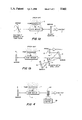
- FIGS. 1a and 1b schematically show the respective layouts of a conventional Q-switched laser and a conventional cavity dumped laser.
- FIG. 2a schematically depicts a single crystal structure fabricated from one of the oxide compounds in the group.
- FIG. 2b is a schematic of another embodiment, wherein a thin film of the compound is sandwiched between transparent materials.
- FIGS. 3a through 3d consist of four schematics embodying differing forms of stimuli; in which 3a shows radial hydrostatic pressure to an individual crystal, 3b shows the use of hydrostatic pressure with a thin film sandwich, 3c depicts the application of thermal energy, and 3d shows a thin film structure stimulated by an electric field.
- FIG. 4 contains a schematic depiction of a thin film sandwich device used as a laser output coupler at the control of an external voltage source.
- FIGS. 1a and 1b schematically represent two of the many conventional laser configurations, these two being known in the parlance of the art as a Q-switched laser and a cavity dumped laser, respectively.
- rotating mirror 1 is synchronized with the transmission of luminous energy 3 from flash lamp type pump 2 into gain medium 4 of the laser's resonating cavity.
- Output coupling mirror 6 normally transmits about 30% of the incident luminous energy, reflecting the remainder back into gain medium 4.
- laser output 7 consists of pulses having a repetition rate corresponding to the rotation rate of mirror 1.
- the cavity dumped configuration in FIG. 1b extracts a laser pulse by deflecting the luminous energy beam.
- pump 2 supplies luminous energy 3 to gain medium 4 of the laser resonating cavity.
- gain medium 4 At one end of gain medium 4 is stationary mirror 8, while the luminous path from the other end of gain medium 4 communicates with mirror 9, acousto-optic modulator 11, mirror 12, and at times prism 13. Since the configuration in FIG. 1b is well known, it need only be noted that stimulation of acousto-optic modulator 11 alters the path of incident luminous energy onto the path defined by reference line 16. Without stimulation, luminous energy passing through acousto-optic modulator 11 follows the path defined by dashed line 14, effectively being retroreflective as to gain medium 4.
- the central feature of the invention is a utilization of oxide compounds from a defined group to directly control the luminous energy leaving the resonating cavity of a laser.
- compounds from this group When stimulated, compounds from this group respond by undergoing a transition between metallic and non-metallic states, which correspond to reflection or transmission of the incident luminous energy.
- the compounds to which this invention pertains are generally semiconducting oxides of elements found in Group VB or IVB of the periodic table, and are further characterized by their narrow 3d bands and energy gaps ranging from 0.1 to 0.4 ev.
- the group consists of VO, VO 2 , V 2 O 3 , V 4 O 7 , V 5 O 9 , V 6 O 11 , V 7 O 13 , V 8 O 15 , Ti 2 O 3 , Ti 4 O 7 , V 3 O 5 , NbO 2 , FeSi 2 , VO 2 NbO 2 , V 1-x Mo x O 2 , VO 2 -TiO 2 , V 2 O 3 -Ti 2 O 3 , V 1-x Ge x O 2 , V 1-x Nb x O 2 , V 1-x Cr x O 2 , (Cr x V 1-x ) 2 O 3 and V 1-x Ti x O 2 .
- the materials may be fabricated in the form of a single crystal, as shown by reference 17 in FIG. 2a, or may take the form of a thin film, such as thin film 18 sandwiched between layers 19 and 21 of transparent material.
- the latter embodiment is schematically depicted in FIG. 2b.
- FIG. 3a depicts the application of radial pressure 22 to single crystal 17.
- the stimulation in FIG. 3b is analogous, where hydrostatic pressure 24 is applied to exterior layers 19 and 21 to compress thin film 18 sandwiched therebetween.
- thermal energy 26, depicted schematically in FIG. 3c, can be used with either structural form.
- FIG. 3d shows the preferred embodiment hereof in the form of a thin film, 18, of a compound from the group sandwiched between transparent exterior layers 19 and 21.
- This schematic also shows the presence of two electrically conductive intermediate layers 25 and 30, and an external voltage supply 27 attached thereto.
- Conductive layers 25 and 30 would preferably be thin electrically conducting films fabricated from materials which are transparent at the wavelength of the luminous energy transmitted through the device. For example if operation is desired in the infrared region of the spectrum, conductors made of In 2 O 3 or Sb would be appropriate.
- voltage 27 in the manner described creates an electric field across thin film 18 of the transition material.
- the relative magnitudes of voltage needed to induce transition consider the compound VO 2 .
- voltage magnitudes ranging from 10 to 50 volts and electric current flows from 1 to 50 milliamperes are typical of that which is necessary to trigger a phase transition.
- voltage source 27 is not restricted to a fixed value but may, when the application demands, include repetitive short duration pulses, either synchronized or free running.
- Stimulation by the imposition of an electric field is not limited to structures in which the oxide compounds take the form of a thin film. If patterns of electrodes are plated or otherwise deposited onto two faces of a single crystal structure, the composite is amenable to stimulation by the electric field formed when a voltage is applied between the electrodes.
- the central feature of the invention resides in the utilization of the above-described materials and devices to modulate, and thereby control, the luminous energy output from a laser resonating cavity.
- FIG. 4 A schematic representation of one such embodiment appears in FIG. 4, where output coupler 28 is shown to be of the thin film sandwich configuration.
- Voltage control 29 is analogous to voltage source 27 in FIG. 3d, altered as necessary to synchronize with pump 2.
- Lasing of the resonating cavity in FIG. 4 commences when pump 2 has introduced sufficient energy 3 into gain medium 4 and output coupler 28 is stimulated into a reflective state. Luminous energy output 31 appears after voltage control 28 alters the stimulus to output coupler 28 sufficiently to cause a transition from the reflective state into the transmissive state.
- the configuration depicted in FIG. 4, and described with reference thereto, is operated in the mode commonly known as cavity dumped. Equally feasible is a Q-switched configuration of the general form depicted in FIG. 1a, in which the reflective function of rotating mirror 1 is performed by a phase transition material coupler element in changing from its transmissive state to its metallic state. In either case, the luminous energy output from the laser cavity is in the form of repetitive pulses, the rate of which is determined by the transition time between the reflective and non-reflective couplers rates.
Landscapes
- Physics & Mathematics (AREA)
- Electromagnetism (AREA)
- Engineering & Computer Science (AREA)
- Plasma & Fusion (AREA)
- Optics & Photonics (AREA)
- Lasers (AREA)
Abstract
An optical modulator particularly suited for use as an output coupler from the resonating cavity of a laser. The modulator is fabricated with a semiconducting oxide compound selected from the group consisting of VO, VO2, V2 O3, V3 O5, V4 O6, V5 O9, V6 O11, V7 O13, V8 O15, Ti2 O3, Ti4 O7, NbO2, FeSi2, VO2 NbO2, V1-x Mox O2, VO2 -TiO2, V2 O3 -Ti2 O3, V1-x Gex O2, V1-x Nbx O2, V1-x Crx O2, (Crx V1-x)2 O3 and V1-x Tix O2. When an electric field is applied to an output coupler fabricated with a thin film or single crystal of material from the foregoing group, the material undergoes a transition between metallic and semiconducting states. In the metallic state the output coupler reflects incident luminous energy. In the semiconducting state, on the other hand, the material transmits such luminous energy. Thereby, a laser system output coupler fabricated with a material from the above-defined group can, by external stimulation, be caused to reflect back or transmit out the laser energy stored within the resonating cavity. Furthermore, since transition between states can be performed with speeds ranging from microseconds to nanoseconds, the output coupler is compatible with the needs of Q-switched or cavity dumped laser configurations.
Description
The invention described herein may be manufactured and used by or for the Government of the United States for all governmental purposes without the payment of any royalty.
This application is a continuation-in-part of copending application assigned Ser. No. 06/139,070 and filed Apr. 10, 1980, now abandoned, which was a continuation-in-part of an application assigned Ser. No. 965,464 and filed on Nov. 30, 1978, now abandoned.
1. Field of the Invention
The invention disclosed herein relates to modulators of luminous energy typified by that generated in lasers, and particularly those modulators fabricated with oxide compounds which undergo transitions between metallic and non-metallic states in response to external stimuli.
2. Description of the Prior Art
Modulators of luminous energy radiating in the infrared, visible and ultraviolet spectra are, as a general premise, known by those skilled in the related arts. Likewise, lasers and means for their control are generally known. What is lacking is a laser system luminous energy modulator which can be inserted into the output path of a laser and operate as a reflective mirror or output coupler, translating between states at the behest of an external control with sufficient speed to generate pulsed laser outputs.
The related art known to the inventor appears in U.S. Pat. No. 3,455,627 granted to inventor Eugene C. Letter and U.S. Pat. No. 3,656,836 granted to joint inventors Baudoin de Cremoux and Pierre Leclerc. The teachings of the patent to Letter disclose an optical element which alternates between reflecting and absorbing states in response to the thermal effects of high energy density luminous radiation. The transition is a self-initiated thermal phenomenon, with the device reverting to its prior state upon the dissipation of the thermal energy added by the incident radiation.
The other patent, de Cremoux et al, also addresses the modulation of luminous energy. The device disclosed in this patent is defined to undergo transition between a first transmission state and a second absorption state upon the formation of an electric field within the semiconductor material constituting the device. Thereby, the modulation characteristics of this device are readily amenable to external control.
Neither of the foregoing disclosures describe a modulating device particularly suited to the job of extracting luminous energy from the resonating cavity of a laser. Notwithstanding the multiplicity of known techniques for accomplishing such an objective, none approach the simplicity or efficiency of a device which can be induced to undergo transitions between highly reflective and transmissive states.
The subject matter of this invention is a particular group of semiconducting materials and their implementation to controllably extract luminous energy from the resonating cavity of a laser. Unlike the many complex and often inefficient techniques utilized by those practicing in the art, a device appropriately fabricated with one or more of the semiconductor materials from a group consisting of VO, VO2, V2 O3, V3 O5, V4 O7, V5 O9, V6 O11, V7 O13, V8 O15, Ti2 O3, Ti4 O7, NbO2, FeSi2, VO2 NbO2, V1-x Mox O2, VO2 -TiO2, V2 O3 -Ti2 O3, V1-x Gex O2, V1-x Nbx O2, V1-x Crx O2 ; (Crx V1-x)2 O3 and V1-x Tix O2 can perform analogous operations. The oxide compounds forming the group are generally characterized by their narrow 3d bands and, typically, energy gaps within the range extending from 0.1 eV to 0.4 eV. A further common trait is their periodic table location, wherein the compounds tend to be oxides of elements in either group VB or IVB.
The compounds constituting this group undergo a phase transition in response to externally introduced stimuli of thermal energy, hydrostatic pressure or electric field. The phase change exhibited is between metallic and non-metallic states, which, as a general rule, are coextensive with their being highly reflective or nonreflective (transmissive) to incident luminous energy.
When a compound from this group is used in the fabrication of an output coupler for a laser resonating cavity, it functions as the cavity mirror while in the reflective state and as a substantially transparent output window when stimulated into its transmissive state. The simplicity of this single device is strikingly apparent when it is compared to the conventional methods of extracting laser energy from the gain medium of a laser resonating cavity.
The semiconducting oxide compounds from the above defined group may be fabricated as individual crystals or thin films, the latter being deposited onto a transparent substrate or sandwiched between layers thereof.
Another characteristic exhibited by this group of compounds, further accentuating their suitability for laser applications, resides in the abrupt rate of the transition between states. When appropriately controlled by means of the prescribed stimuli, pulse widths ranging from microseconds to nanoseconds, with repetition rates in the range of megahertz, are fully contemplated.
FIGS. 1a and 1b schematically show the respective layouts of a conventional Q-switched laser and a conventional cavity dumped laser.
FIG. 2a schematically depicts a single crystal structure fabricated from one of the oxide compounds in the group.
FIG. 2b is a schematic of another embodiment, wherein a thin film of the compound is sandwiched between transparent materials.
FIGS. 3a through 3d consist of four schematics embodying differing forms of stimuli; in which 3a shows radial hydrostatic pressure to an individual crystal, 3b shows the use of hydrostatic pressure with a thin film sandwich, 3c depicts the application of thermal energy, and 3d shows a thin film structure stimulated by an electric field.
FIG. 4 contains a schematic depiction of a thin film sandwich device used as a laser output coupler at the control of an external voltage source.
FIGS. 1a and 1b schematically represent two of the many conventional laser configurations, these two being known in the parlance of the art as a Q-switched laser and a cavity dumped laser, respectively. In the Q-switched laser of FIG. 1a rotating mirror 1 is synchronized with the transmission of luminous energy 3 from flash lamp type pump 2 into gain medium 4 of the laser's resonating cavity. When mirror 1 rotates into alignment, lasing commences. Output coupling mirror 6 normally transmits about 30% of the incident luminous energy, reflecting the remainder back into gain medium 4. Thereby, laser output 7 consists of pulses having a repetition rate corresponding to the rotation rate of mirror 1.
The cavity dumped configuration in FIG. 1b extracts a laser pulse by deflecting the luminous energy beam. As with the Q-switched configuration pump 2 supplies luminous energy 3 to gain medium 4 of the laser resonating cavity. At one end of gain medium 4 is stationary mirror 8, while the luminous path from the other end of gain medium 4 communicates with mirror 9, acousto-optic modulator 11, mirror 12, and at times prism 13. Since the configuration in FIG. 1b is well known, it need only be noted that stimulation of acousto-optic modulator 11 alters the path of incident luminous energy onto the path defined by reference line 16. Without stimulation, luminous energy passing through acousto-optic modulator 11 follows the path defined by dashed line 14, effectively being retroreflective as to gain medium 4.
The central feature of the invention is a utilization of oxide compounds from a defined group to directly control the luminous energy leaving the resonating cavity of a laser. When stimulated, compounds from this group respond by undergoing a transition between metallic and non-metallic states, which correspond to reflection or transmission of the incident luminous energy.
The compounds to which this invention pertains are generally semiconducting oxides of elements found in Group VB or IVB of the periodic table, and are further characterized by their narrow 3d bands and energy gaps ranging from 0.1 to 0.4 ev. In particular, the group consists of VO, VO2, V2 O3, V4 O7, V5 O9, V6 O11, V7 O13, V8 O15, Ti2 O3, Ti4 O7, V3 O5, NbO2, FeSi2, VO2 NbO2, V1-x Mox O2, VO2 -TiO2, V2 O3 -Ti2 O3, V1-x Gex O2, V1-x Nbx O2, V1-x Crx O2, (Crx V1-x)2 O3 and V1-x Tix O2.
Structurally, the materials may be fabricated in the form of a single crystal, as shown by reference 17 in FIG. 2a, or may take the form of a thin film, such as thin film 18 sandwiched between layers 19 and 21 of transparent material. The latter embodiment is schematically depicted in FIG. 2b.
All materials in the defined group exhibit a transition phenomenon in response to externally introduced stimuli of hydrostatic pressure, thermal energy or electric field. FIG. 3a depicts the application of radial pressure 22 to single crystal 17. The stimulation in FIG. 3b is analogous, where hydrostatic pressure 24 is applied to exterior layers 19 and 21 to compress thin film 18 sandwiched therebetween. The use of thermal energy 26, depicted schematically in FIG. 3c, can be used with either structural form.
Although it is recognized that the transition will occur under an imposed thermal or pressure stimulus, the utility of the output coupler of the present invention resides in its ability to transition at controllably repetetive rates in the megahertz range under an applied electrical stimulus. Therefore, FIG. 3d, shows the preferred embodiment hereof in the form of a thin film, 18, of a compound from the group sandwiched between transparent exterior layers 19 and 21. This schematic also shows the presence of two electrically conductive intermediate layers 25 and 30, and an external voltage supply 27 attached thereto. Conductive layers 25 and 30 would preferably be thin electrically conducting films fabricated from materials which are transparent at the wavelength of the luminous energy transmitted through the device. For example if operation is desired in the infrared region of the spectrum, conductors made of In2 O3 or Sb would be appropriate.
The application of voltage 27 in the manner described creates an electric field across thin film 18 of the transition material. As an example of the relative magnitudes of voltage needed to induce transition, consider the compound VO2. For a thin film of this particular material used in a relatively small output coupler voltage magnitudes ranging from 10 to 50 volts and electric current flows from 1 to 50 milliamperes are typical of that which is necessary to trigger a phase transition. Furthermore, since the transition between states is very abrupt, voltage source 27 is not restricted to a fixed value but may, when the application demands, include repetitive short duration pulses, either synchronized or free running.
Stimulation by the imposition of an electric field is not limited to structures in which the oxide compounds take the form of a thin film. If patterns of electrodes are plated or otherwise deposited onto two faces of a single crystal structure, the composite is amenable to stimulation by the electric field formed when a voltage is applied between the electrodes.
As noted previously, the central feature of the invention resides in the utilization of the above-described materials and devices to modulate, and thereby control, the luminous energy output from a laser resonating cavity. A schematic representation of one such embodiment appears in FIG. 4, where output coupler 28 is shown to be of the thin film sandwich configuration. Voltage control 29 is analogous to voltage source 27 in FIG. 3d, altered as necessary to synchronize with pump 2.
Lasing of the resonating cavity in FIG. 4 commences when pump 2 has introduced sufficient energy 3 into gain medium 4 and output coupler 28 is stimulated into a reflective state. Luminous energy output 31 appears after voltage control 28 alters the stimulus to output coupler 28 sufficiently to cause a transition from the reflective state into the transmissive state. The configuration depicted in FIG. 4, and described with reference thereto, is operated in the mode commonly known as cavity dumped. Equally feasible is a Q-switched configuration of the general form depicted in FIG. 1a, in which the reflective function of rotating mirror 1 is performed by a phase transition material coupler element in changing from its transmissive state to its metallic state. In either case, the luminous energy output from the laser cavity is in the form of repetitive pulses, the rate of which is determined by the transition time between the reflective and non-reflective couplers rates.
Those skilled in the art will recognize the degree of simplification attained when a single output coupler, 28, replaces the plethora of optical and mechanical devices previously needed to regulate the luminous energy output from a comparable laser resonating cavity. A single device now accomplishes that which took rotating apertures, Kerr cells, Pocket effect crystals, dyes or destructable films in conventional lasers. Furthermore, the output coupler undergoes transition at the behest of an external control, and as such is operable repeatedly without degradation, thus being in distinct contrast to uncontrollable output coupling materials, such as germanium, which deteriorate rapidly with successive output pulses.
Claims (3)
1. An output coupler for the resonating cavity of a repetitively pulsed laser, comprising:
a. an optical device for controllably reflecting and transmitting luminous energy repetitively in response to an externally applied electric field, said device comprising a material selected from the group consisting of VO, VO2, V2 O3, V3 O5, V4 O7, V5 O9, V6 O11, V7 O13, V8 O15, Ti2 O3, Ti4 O7, NbO2, FeSi2, VO2 NbO2, V1-x Mox O2, VO2 -TiO2, V2 O3 -Ti2 O3, V1-x Gex O2, V1-x Nbx O2, V1-x Crx O2, (Crx V1-x)2 O3 and V1-x Tix O2 ; and
b. means for selectively applying an electric field across said device whereby said optical device material is selectively stimulated to transition between the metallic, optically reflective state and the semiconducting, optically transmissive state.
2. The output coupler as recited in claim 1, wherein said optical device further comprises a thin film of said material sandwiched between substrates which are transparent to said luminous energy.
3. The output coupler as recited in claims 1 or 2, wherein said means for applying an electric field across said optical device material comprises two substantially transparent juxtaposed metallic electrodes deposited on said material and locating said material therebetween, and a controllable source of electric voltage connected across said electrodes.
Priority Applications (1)
| Application Number | Priority Date | Filing Date | Title |
|---|---|---|---|
| US06/401,162 USH461H (en) | 1978-11-30 | 1982-07-23 | Non-reflective/reflective phase transition optical modulator |
Applications Claiming Priority (2)
| Application Number | Priority Date | Filing Date | Title |
|---|---|---|---|
| US96546478A | 1978-11-30 | 1978-11-30 | |
| US06/401,162 USH461H (en) | 1978-11-30 | 1982-07-23 | Non-reflective/reflective phase transition optical modulator |
Related Parent Applications (1)
| Application Number | Title | Priority Date | Filing Date |
|---|---|---|---|
| US06139070 Continuation-In-Part | 1980-04-10 |
Publications (1)
| Publication Number | Publication Date |
|---|---|
| USH461H true USH461H (en) | 1988-04-05 |
Family
ID=27017320
Family Applications (1)
| Application Number | Title | Priority Date | Filing Date |
|---|---|---|---|
| US06/401,162 Abandoned USH461H (en) | 1978-11-30 | 1982-07-23 | Non-reflective/reflective phase transition optical modulator |
Country Status (1)
| Country | Link |
|---|---|
| US (1) | USH461H (en) |
Cited By (5)
| Publication number | Priority date | Publication date | Assignee | Title |
|---|---|---|---|---|
| US5212741A (en) * | 1992-01-21 | 1993-05-18 | Eastman Kodak Company | Preprocessing of dot-matrix/ink-jet printed text for Optical Character Recognition |
| US6021153A (en) * | 1998-03-12 | 2000-02-01 | Sumitomo Electric Industries, Ltd. | Variable-curvature reflecting mirror |
| US6744790B1 (en) * | 1995-08-31 | 2004-06-01 | Biolase Technology, Inc. | Device for reduction of thermal lensing |
| US8655189B2 (en) * | 2010-06-18 | 2014-02-18 | Exelis, Inc. | Optical modulation utilizing structures including metamaterials |
| CN103996969A (en) * | 2014-05-29 | 2014-08-20 | 山东大学 | Layered VO2 laser pulse modulation device and its application |
Citations (12)
| Publication number | Priority date | Publication date | Assignee | Title |
|---|---|---|---|---|
| US3371978A (en) | 1964-02-12 | 1968-03-05 | North American Aviation Inc | Pressure-sensitive optical cell |
| US3379998A (en) | 1964-07-09 | 1968-04-23 | Jack A. Soules | Laser image amplifying system |
| US3426294A (en) | 1965-02-10 | 1969-02-04 | American Optical Corp | Laser q-switching |
| US3455627A (en) | 1965-01-04 | 1969-07-15 | Bausch & Lomb | Optical element |
| US3484722A (en) | 1966-11-23 | 1969-12-16 | Bell Telephone Labor Inc | Optical modulator |
| US3497286A (en) | 1966-11-23 | 1970-02-24 | Bell Telephone Labor Inc | Variable reflectance display device |
| US3521941A (en) | 1967-02-07 | 1970-07-28 | American Cyanamid Co | Electro-optical device having variable optical density |
| US3555455A (en) | 1968-08-29 | 1971-01-12 | Nasa | Method and apparatus for optical modulating a light signal |
| US3656836A (en) | 1968-07-05 | 1972-04-18 | Thomson Csf | Light modulator |
| US3664726A (en) | 1969-10-21 | 1972-05-23 | Univ Yeshiva | Optical shutter for laser or maser modulation |
| US3879108A (en) | 1971-12-23 | 1975-04-22 | American Cyanamid Co | Electrochromic devices |
| US3971874A (en) | 1973-08-29 | 1976-07-27 | Matsushita Electric Industrial Co., Ltd. | Optical information storage material and method of making it |
-
1982
- 1982-07-23 US US06/401,162 patent/USH461H/en not_active Abandoned
Patent Citations (12)
| Publication number | Priority date | Publication date | Assignee | Title |
|---|---|---|---|---|
| US3371978A (en) | 1964-02-12 | 1968-03-05 | North American Aviation Inc | Pressure-sensitive optical cell |
| US3379998A (en) | 1964-07-09 | 1968-04-23 | Jack A. Soules | Laser image amplifying system |
| US3455627A (en) | 1965-01-04 | 1969-07-15 | Bausch & Lomb | Optical element |
| US3426294A (en) | 1965-02-10 | 1969-02-04 | American Optical Corp | Laser q-switching |
| US3484722A (en) | 1966-11-23 | 1969-12-16 | Bell Telephone Labor Inc | Optical modulator |
| US3497286A (en) | 1966-11-23 | 1970-02-24 | Bell Telephone Labor Inc | Variable reflectance display device |
| US3521941A (en) | 1967-02-07 | 1970-07-28 | American Cyanamid Co | Electro-optical device having variable optical density |
| US3656836A (en) | 1968-07-05 | 1972-04-18 | Thomson Csf | Light modulator |
| US3555455A (en) | 1968-08-29 | 1971-01-12 | Nasa | Method and apparatus for optical modulating a light signal |
| US3664726A (en) | 1969-10-21 | 1972-05-23 | Univ Yeshiva | Optical shutter for laser or maser modulation |
| US3879108A (en) | 1971-12-23 | 1975-04-22 | American Cyanamid Co | Electrochromic devices |
| US3971874A (en) | 1973-08-29 | 1976-07-27 | Matsushita Electric Industrial Co., Ltd. | Optical information storage material and method of making it |
Non-Patent Citations (5)
| Title |
|---|
| "Valiev et al, "Metal-Insulator . . . Field", 1970, pp. 18-22, Pis'ma Zh. Eksp. Teor. Fig. 12.1. |
| J. C. C. Fan et al, "Thin-Film VO2 Submillimeter-Wave Modulators and Polarizersa)" Applied Physics Ltr, vol. 31, No. 1, Jul. 1, 1977, pp. 11-13. |
| P. G. Eliseev & M. A. Man'ko "Use of a Semiconductor Mirror for Laser Q-Switching", Soviet Physics-Tech Physics, vol. 11, No. 12, Jun. 1967, pp. 1657-1658. |
| Vos, "Reflectance & Electroreflectance of TiO2 Single Crystals . . . "J. Phys. C. Solid State Phys., vol. 10(19), 1977, pp. 3917-3918. |
| Weiser et al., "Optically Erasing . . . Switchable Film", 12/73, pp. 2075-2076, IBM Tech. Disc. Bull., vol. 13, #7. |
Cited By (6)
| Publication number | Priority date | Publication date | Assignee | Title |
|---|---|---|---|---|
| US5212741A (en) * | 1992-01-21 | 1993-05-18 | Eastman Kodak Company | Preprocessing of dot-matrix/ink-jet printed text for Optical Character Recognition |
| US6744790B1 (en) * | 1995-08-31 | 2004-06-01 | Biolase Technology, Inc. | Device for reduction of thermal lensing |
| US6021153A (en) * | 1998-03-12 | 2000-02-01 | Sumitomo Electric Industries, Ltd. | Variable-curvature reflecting mirror |
| US8655189B2 (en) * | 2010-06-18 | 2014-02-18 | Exelis, Inc. | Optical modulation utilizing structures including metamaterials |
| CN103996969A (en) * | 2014-05-29 | 2014-08-20 | 山东大学 | Layered VO2 laser pulse modulation device and its application |
| CN103996969B (en) * | 2014-05-29 | 2017-08-08 | 山东大学 | Stratiform VO2Laser pulse modulator device and application |
Similar Documents
| Publication | Publication Date | Title |
|---|---|---|
| US4059759A (en) | Passive and active pulse stacking scheme for pulse shaping | |
| US3208342A (en) | Electro-optic light coupling of optical fibers | |
| US4529273A (en) | Passive phase conjugate mirror | |
| GB1363143A (en) | Polarization independent light modulation means using birefringent crystals | |
| US4558923A (en) | Picosecond bistable optical switch using two-photon transitions | |
| EP0275554B1 (en) | Optical device | |
| US4085335A (en) | Optical parametric device | |
| USH461H (en) | Non-reflective/reflective phase transition optical modulator | |
| US3918007A (en) | Fabry-perot polarization laser beam modulator | |
| US4233569A (en) | High power laser with tuning and line narrowing capability | |
| EP0131042B1 (en) | Intensity of a light beam applied to a layered semiconductor structure controls the beam | |
| Channin | Triode optical gate: A new liquid crystal electro‐optic device | |
| US3928814A (en) | Collinear acousto-optical tunable filter and acousto-optically tunable laser | |
| EP0324434B1 (en) | Method of activating a nonlinear optical element having electrodes on two side surfaces of nonlinear medium through insulating layers | |
| JPH05283804A (en) | Optical pulse generator | |
| JPH0375848B2 (en) | ||
| EP0434139B1 (en) | Frequency doubling optical waveguide with active phase matching | |
| US4372653A (en) | Polarizing beam splitting phase transition optical modulator | |
| US3902137A (en) | Electro-optic diffraction grating tuned laser | |
| US5028816A (en) | Electro-optic line narrowing of optical parametric oscillators | |
| US5046803A (en) | Actively phased matched frequency doubling optical waveguide | |
| US3500237A (en) | Mode coupling laser apparatus | |
| US3789318A (en) | Stimulated emission radiation source with adjustable wavelength | |
| Guo et al. | Quasi-velocity-matched electrooptic phase modulator for the synthesis of ultrashort optical pulses | |
| RU2040090C1 (en) | Scanning laser |
Legal Events
| Date | Code | Title | Description |
|---|---|---|---|
| STCF | Information on status: patent grant |
Free format text: PATENTED CASE |